WO2020137540A1 - 周波数選択板 - Google Patents
周波数選択板 Download PDFInfo
- Publication number
- WO2020137540A1 WO2020137540A1 PCT/JP2019/048427 JP2019048427W WO2020137540A1 WO 2020137540 A1 WO2020137540 A1 WO 2020137540A1 JP 2019048427 W JP2019048427 W JP 2019048427W WO 2020137540 A1 WO2020137540 A1 WO 2020137540A1
- Authority
- WO
- WIPO (PCT)
- Prior art keywords
- resonator
- frequency
- pattern
- conductive pattern
- electrode plate
- Prior art date
- Legal status (The legal status is an assumption and is not a legal conclusion. Google has not performed a legal analysis and makes no representation as to the accuracy of the status listed.)
- Ceased
Links
Images






Classifications
-
- H—ELECTRICITY
- H01—ELECTRIC ELEMENTS
- H01Q—ANTENNAS, i.e. RADIO AERIALS
- H01Q15/00—Devices for reflection, refraction, diffraction or polarisation of waves radiated from an antenna, e.g. quasi-optical devices
- H01Q15/14—Reflecting surfaces; Equivalent structures
-
- H—ELECTRICITY
- H01—ELECTRIC ELEMENTS
- H01Q—ANTENNAS, i.e. RADIO AERIALS
- H01Q15/00—Devices for reflection, refraction, diffraction or polarisation of waves radiated from an antenna, e.g. quasi-optical devices
- H01Q15/14—Reflecting surfaces; Equivalent structures
- H01Q15/148—Reflecting surfaces; Equivalent structures with means for varying the reflecting properties
Definitions
- the present invention relates to a frequency selection plate having a structure in which resonators of the same shape are periodically arranged on a dielectric substrate.
- Information communication equipment is becoming smaller and more sophisticated, and wireless communication services using lines such as wireless LAN and LTE are rapidly spreading. Along with this, the transmission and reception of radio waves from the wireless communication terminal have become widespread and frequently performed, and there is a concern that other electronic devices in the vicinity will be affected.
- the frequency selection plate has frequency dependence in the transmission characteristics/reflection characteristics of an incident electromagnetic wave by periodically arranging resonators (unit cells) formed of a conductor pattern having a size equal to or less than the wavelength. It is a thing.
- the frequency selection plate has a resonant structure with various frequency characteristics.
- those having a band-stop filter characteristic of reflecting only a specific frequency are mainly those having a resonant structure in a conductor portion, such as a ring type, a dipole array type, a trihole type, a patch type, and a Jerusalem cross type.
- Non-patent document 1 those having a band-stop filter characteristic of reflecting only a specific frequency are mainly those having a resonant structure in a conductor portion, such as a ring type, a dipole array type, a trihole type, a patch type, and a Jerusalem cross type.
- the frequency selection board has a large number of structural parameters to be considered, and the parameters may be contradictory to the increase and decrease of the inductance component and the capacitance component.
- the characteristics change depending on how the unit cells are arranged, which is theoretically complicated (Non-Patent Document 2).
- the present invention has been made in view of this problem, and an object thereof is to provide a frequency selection plate whose operating frequency and bandwidth can be easily adjusted.
- a frequency selection plate is a frequency selection plate having a structure in which resonators formed of conductive patterns of the same shape are periodically arranged on a dielectric substrate, wherein The horizontal and vertical pattern conductors forming a cross on the body substrate, and both ends of the horizontal and vertical patterns, which are stretched by a predetermined length, are extended and extended in orthogonal directions.
- the tip portion is provided with a tip portion extending from the other direction and a pole plate portion having a shape diagonally opposed to each other, and the pole plate portion is a center facing the pole plate portion of another adjacent resonator.
- a portion is cut out with the width of the horizontal pattern, and a width that is narrower than the width of the horizontal pattern and shorter than the predetermined length is extended from the center of the cutout portion of another resonator adjacent to the resonator.
- the gist of the present invention is that the tip portion is joined to the electrode plate portion, and the distance between the tip portions is wider than the distance between the electrode plate portion of another resonator adjacent thereto.
- FIG. 8 is a diagram showing a capacitive component forming a sub resonator of the frequency selection plate shown in FIG. 7. It is a figure which shows the equivalent circuit of the frequency selection board shown in FIG. FIG. 8 is a diagram showing a change in cutoff frequency when the shape of the conductive pattern of the sub-resonator shown in FIG. 7 is changed. It is a figure which shows the one part plane of the frequency selection board which concerns on 3rd Embodiment of this invention. An equivalent circuit in which the capacitance component is connected in parallel to the equivalent circuit of the low-frequency side bandpass resonator is shown.
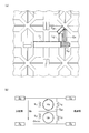
- FIG. 1 is a diagram schematically showing a part of a plane of a frequency selection plate according to the first embodiment of the present invention.
- the frequency selection plate 100 shown in FIG. 1 is configured by periodically arranging resonators k xy formed on a dielectric substrate 101 with a conductive pattern having a shape similar to the Chinese character “T”.
- the x direction is defined as horizontal and the y direction is defined as vertical.
- the dielectric substrate 101 is composed of, for example, a glass epoxy substrate, a polyimide film substrate, or the like.
- the dielectric substrate 101 may be made of any material as long as it is a dielectric material.
- a conductive film 102 is formed on the dielectric substrate 101.
- the resonator k xy (conductive pattern) having a predetermined shape may be formed by vapor deposition on the dielectric substrate 101, or the conductive film 102 may be formed on the entire surface of the dielectric substrate 101 and then etched. You may form it.
- 10 resonators k xy are arranged in each of the x direction and the y direction to form the frequency selection plate 100.
- the size of one resonator k xy is about 1/3 of the wavelength of the resonance frequency.
- the signal is input to the frequency selection plate 100 from the ⁇ z direction (back side) and output (transmitted) in the z direction (front side).
- an electromagnetic wave is input to the frequency selection plate 100, an electric field is generated on the xy plane where the resonators k xy are arranged, and a current due to the resonance phenomenon flows.
- the configuration of the resonator k xy will be described in relation to the resonator k (x+1)y that is adjacent in the +x direction.
- the conductor portions of the horizontal pattern 10 and the vertical pattern 20 that form a cross on the dielectric substrate 101, and both ends of the horizontal pattern 10 and the vertical pattern 20 that are extended by a predetermined length are extended (12a, 12b) in a direction orthogonal to each other, and the tip portion includes a tip portion extended from the other direction and a polar plate portion 12 having a shape which is diagonally opposed to the tip portion with a space D therebetween.
- a central portion facing the electrode plate portion 11 of another adjacent resonator k (x+1)y is cut out by the width of the horizontal pattern 10 (cutout portion 13), and the cutout portion 13 is formed.
- a width narrower than the width of the horizontal pattern 10 and shorter than the width of the horizontal pattern 10 extending from the center of the adjacent pattern to join with the electrode plate portion 11 of another adjacent resonator k (x+1)y (conductor pattern 14). ..
- the distance D between the tip portions of the conductor patterns 12a and 12b extended in the direction orthogonal to the horizontal pattern 10 is wider than the distance d between the adjacent resonator plate k (x+1)y and the electrode plate portion 11. is there.
- the planar shape of the electrode plate portion 12 is a trapezoid having the outer bottom as the bottom and the inner side as the top, and the center portion of the bottom is notched, and the center of the notch 13 in the y direction.
- the cutout portion 13 is divided into two cutout portions 13 a and 13 b by the conductor pattern 14.
- each resonator k xy is vertically symmetrical with respect to the center line of the horizontal pattern 10. Further, it is symmetrical with respect to the center line of the vertical pattern 20.
- the frequency selection plate 100 includes resonance paths through which three resonance currents flow.
- FIG. 2 is a diagram schematically showing a resonance path in which three resonance currents flowing in the frequency selection plate 100 flow.
- the three resonance currents are the stop band path Sb in which the resonance current of the cutoff frequency (operating frequency) f Sb which is the series resonance frequency flows, and the resonance current of the parallel resonance frequency on the low frequency side (the low frequency side band pass frequency f Lb ).
- the low frequency band pass path Lb constitutes the low frequency band pass resonator k Lb.
- the high frequency band pass path Hb constitutes a high frequency band pass resonator k Hb .
- the stop band path Sb is a path that passes through the horizontal pattern 10 and the vertical pattern 20 of the adjacent resonators k xy .
- FIG. 2 only the route on the +y side in the x direction is shown because the drawing is complicated.
- the actual stop band path Sb exists symmetrically about the horizontal pattern 10 in the -y direction. Further, the vertical pattern 20 exists also in the ⁇ x directions.
- the low-frequency side band pass path Lb is a path that circulates around the cutouts 13a of the adjacent resonators k xy .
- FIG. 2 only the path on the +y side in the x direction is shown like the stop band path Sb.
- the actual low-frequency side bandpass path Lb exists symmetrically in the ⁇ y direction with the horizontal pattern 10 as the center. Further, the vertical pattern 20 exists also in the ⁇ x directions.
- the high frequency side band pass path Hb is a path that goes around the electrode plate portions 12a and 21b that make the tip portions of one resonator k xy face each other.
- FIG. 3 is a diagram schematically showing the portions of the resonant component of the inductive component and the capacitive component that constitute each resonance path on the resonator k xy .
- the induction component is represented by L and the capacitance component is represented by C.
- FIG. 3( a) is a diagram showing a rough shape of a part constituting each component by enclosing it with a broken line.
- FIG. 3B is a diagram showing each resonance path by an equivalent circuit.
- the stop band path Sb is a resonance in which the inductive component L1 formed by the horizontal pattern 10 and the vertical pattern 20, the inductive component L2 formed by the electrode plate portion 12a in the direction orthogonal to the horizontal pattern 10, and the electrode plate portion 12a are adjacent to each other. It can be represented by the series connection of the capacitance component C s formed between the electrode plate portion 11 of the container k (x+1) y (the path of the arrow shown in FIG. 3B).
- the low-frequency bandpass path Lb is a path in which the inductive component L3 formed by the conductor pattern 14 connecting the notches 13 in the x direction is connected in parallel to the series connection of the inductive component L2 and the capacitive component C s. Can be represented by (the route shown by the dashed circle in FIG. 3B).
- the series connection of the capacitive component Cph formed at the tip of the conductor patterns 12a and 21b and the inductive component L2 can be represented by a path that is connected in parallel to the capacitive component L1 (FIG. 3(b ) In the path indicated by the dashed-dotted circle).
- the spatial impedance Z 0 shown in FIG. 3B represents spatial impedance.
- the spatial impedance Z 0 is an impedance determined by the dielectric constant and magnetic permeability of vacuum.
- the resonance frequency generated in each path can be determined by a parameter representing the shape of the resonator k xy .
- the parameter is mainly the size of each part that determines the shape of the resonator k xy .
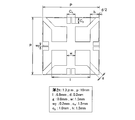
- FIG. 4 is a diagram showing an example of parameters that determine the shape of the resonator k xy .
- the thickness of the conductive pattern is 1.3 ⁇ m.
- the pitch at which the resonators k xy are periodically arranged is 10 mm.
- the length of the horizontal pattern 10 and the vertical pattern 20 is 1, the width of the horizontal pattern 10 and the vertical pattern 20 is w, the length of the electrode plate portion 12 in the x direction is h (the height of the trapezoidal shape), and the width of the cutout portion is Is denoted by c x , the depth of the cutout portion is denoted by c y , the width of the conductive pattern 14 bridging the cutout portion 13 is denoted by w 2 , and the width of the distance D between the tip portions of the electrode plate portions is denoted by g.
- the shape of the resonator k xy including the length of the conductive pattern 14 is determined.
- the above-mentioned inductive component L1, L2, and capacitance component C s, the value of C ph is determined by determining the cavity k xy shape.
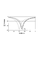
- FIG. 5 shows the analysis result of the resonance frequency of the frequency selection plate shown in FIG.
- the horizontal axis of FIG. 5 is the frequency [GHz], and the vertical axis is the reflection coefficient S 11 [dB] representing the reflection characteristic.
- the cutoff frequency f Sb is the resonance component in which the inductive component L1 formed by the horizontal pattern 10 and the vertical pattern 20, the inductive component L2 formed by the electrode plate portion 12a in the direction orthogonal to the horizontal pattern 10, and the electrode plate portion 12a are adjacent to each other. It is determined by the capacitance component C s formed between the plate portion 11a of the container k (x+1)y and the plate portion 11a. Therefore, the cut-off frequency f Sb is the length l of the horizontal pattern 10 and the vertical pattern 20, the width w of the horizontal pattern 10 and the vertical pattern 20, the pitch p, and the distance from the pole plate portion of another resonator adjacent to the parameter. determined by d.
- FIG. 6 is a diagram showing an example in which the cutoff frequency f Sb changes depending on the capacitance component C s .
- the horizontal axis of FIG. 6 is the frequency [GHz], and the vertical axis is the transmission coefficient S 21 [dB] representing the transmission characteristics.
- the broken line shows the case where the capacitance component C s is increased, and the alternate long and short dash line shows the case where the capacitance component C s is reduced.
- the cutoff frequency f Sb can be changed by the capacitance component C s .
- the low-frequency side transmission frequency f Lb is determined by the width w 2 of the conductive pattern 14 bridging the inside of the notch 13 and the inductive component L3 due to the pitch p, the inductive component L2, and the capacitive component C s .
- the inductive component L2 and the capacitive component C s are also parameters that determine the cutoff frequency f Sb . Therefore, the low-frequency side transmission frequency f Lb can be controlled mainly by the width w 2 of the conductive pattern 14.
- the high frequency side transmission frequency f Hb is determined by the capacitive component C ph and the inductive component L2 formed at the tip portions of the conductor patterns 12a and 21b.
- the induction component L2 is also a parameter that determines the cutoff frequency f Sb . Therefore, the high frequency side transmission frequency f Hb can be controlled mainly by the capacitance component C ph formed at the tips of the conductor patterns 12a and 21b.
- the resonance frequencies of the three resonators can be controlled independently. That is, it is easy to adjust the operating frequency and its bandwidth.
- the frequency selection plate 100 is the frequency selection plate 100 having a structure in which the resonators k xy formed by the conductive patterns of the same shape are periodically arranged on the dielectric substrate 101.
- the conductor portions of the horizontal pattern 10 and the vertical pattern 20 that form a cross on the dielectric substrate 101, and the respective end portions of the horizontal pattern 10 and the vertical pattern 20 that are extended by a predetermined length are provided.
- the tip portion includes a tip portion extending from the other direction and a pole plate portion 12 which is diagonally opposed to the tip portion, and the pole plate portions 12 are adjacent to each other.
- the central portion of the resonator facing the electrode plate portion 11 is notched with the width of the lateral pattern 10, and the width is narrower than the width of the lateral pattern 10 and shorter than a predetermined length from the center of the notched portion 13. It is extended and joined to the pole plate portion 11 of another resonator adjacent thereto, and the distance D between the tip portions of the pole plate portions is wider than the distance d between the pole plate portion of another resonator adjacent thereto. is there. This makes it easier to adjust the operating frequency and its bandwidth.
- the frequency selection plate 100 includes the low-frequency side transmission frequency f Lb and the high-frequency side transmission frequency f Hb around the cutoff frequency f Sb , the low-frequency side transmission frequency f Lb and the high-frequency side transmission frequency f Lb. It can be narrowed blocking characteristic (band-stop characteristics) by approximating the f Hb to the cutoff frequency f Sb.
- FIG. 7 is a figure which shows typically the top view of the frequency selection board which concerns on 2nd Embodiment of this invention.
- the frequency selection plate 200 shown in FIG. 6 differs from the frequency selection plate 100 (FIG. 1) in that it has a sub-resonator.
- the sub-resonator of the frequency selection plate 200 shown in FIG. 7 is formed of, for example, a home-base-shaped second conductive pattern F kp that covers the tip portions of the adjacent electrode plate portions 12 a and 11 a.
- the second conductive pattern F kp is also formed on the tip portions of the electrode plates 21 and 22 in the y direction.
- the second conductive pattern F kp is formed by overlapping the conductive film 102 such as the electrode plate portion 12a with the dielectric layer interposed therebetween.
- a method of superposing the conductive patterns F kp in a layered manner for example, a method in which two resonators k xy and a flexible substrate or a rigid substrate on which the conductive patterns F kp are formed are stacked and mounted, or printed on a PET substrate
- a method is conceivable in which the conductive patterns on one sheet are laminated and fixed in a superposed state.
- it may be manufactured using a semiconductor process for forming a vapor deposition film and a diffusion film.
- FIG. 8 is a diagram schematically showing the structure of the sub-resonator.
- FIG. 7A is a perspective view thereof.
- FIG. 8B is a sectional view taken along the line AA shown in FIG.
- the conductive pattern F kp stacked on the adjacent electrode plate portions 12a and 11a with the dielectric layer interposed therebetween makes it possible to connect the two capacitive components C s ′ in series with each other.
- plate portion 12a is connected in parallel to the capacitive component C s is formed by 11a.
- the capacitance component C s ′ is composed of four layers of a dielectric substrate 101, a conductive film 102, a dielectric film 103, and a second conductive pattern 104. Note that the number of dielectric films and conductive films may be increased. Details will be described later.
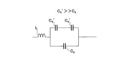
- FIG. 9 is a diagram schematically showing an equivalent circuit of the frequency selection plate 200 including the sub-resonator.
- An equivalent circuit of the resonator k xy (which may be hereinafter referred to as a main resonator) formed of the conductive film 102 is represented by the series connection of the inductive component L and the capacitive component C s .
- the frequency selection plate 200 can be represented by an equivalent circuit in which the series connection of the two capacitance components C s ′ is connected in parallel to the capacitance component C s of the main resonator k xy .
- the capacitance formed between the second conductive pattern F kp and the electrode plate portions 12a and 11a is larger than the capacitance component C s formed between the electrode plate portions 12a and 11a (C s ⁇ C s ). ..
- the cutoff frequency of the frequency selection plate 200 is the frequency to which the capacitive component C s ′ is added. Therefore, the cutoff frequency can be controlled by changing the shape of the second conductive pattern forming the sub-resonator while keeping the shape of the main resonator k xy .
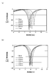
- FIG. 10 is a diagram showing changes in the cutoff frequency when the shape of the second conductive pattern F kp is changed.
- FIG. 10A is a diagram showing a change when the length in the x direction is changed
- FIG. 10B is a diagram showing a change when the length in the y direction is changed.
- the horizontal axis of FIG. 10 is the frequency [GHz]
- the vertical axis is the transmission coefficient S 21 [dB] representing the transmission characteristics.
- the parameter 0 mm in FIG. 10A is for the shape of the second conductive pattern F kp shown in FIG.
- the parameter 0.2 mm represents that the width of the second conductive pattern F kp is set to ⁇ 0.2 mm. That is, the characteristics are obtained when the outer side of one electrode plate portion 12a is -0.1 mm and the outer side of the other electrode plate portion 11a is -0.1 mm.
- the cutoff frequency can be varied within a range of about 1 GHz by changing the width of the second conductive pattern F kp within a range of 0 to 1 mm. That is, the cutoff frequency can be adjusted by changing the shape of the second conductive pattern F kp without changing the shape of the main resonator k xy .
- the parameters 0 mm to 0.5 mm in FIG. 10B represent dimensions in which the length of the second conductive pattern F kp in the y direction is changed.
- the parameter 0 mm is for the shape of the second conductive pattern F kp shown in FIG.
- the cutoff frequency can be varied within a range of about 0.5 GHz by changing the length of the second conductive pattern F kp in the y direction within a range of 0 to 0.5 mm. In this way, the cutoff frequency can be adjusted by changing the length of the second conductive pattern F kp in the y direction.
- the frequency selection plate 200 includes the second conductive pattern disposed on the conductor portion with the dielectric film interposed therebetween, and the planar shape of the second conductive pattern is the adjacent resonance. It is a shape that covers the same portion between the resonators and a shape that covers between the pole plate portions of the same resonator. This allows the cutoff frequency to be adjusted without changing the shape of the main resonator k xy .
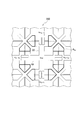
- FIG. 11 is a figure which shows typically the top view of the frequency selection board which concerns on 3rd Embodiment of this invention.
- the frequency selection plate 300 shown in FIG. 11 includes sub-resonators corresponding to the low-frequency side bandpass resonator k Lb and the high-frequency side bandpass resonator k Hb with respect to the frequency selection plate 100 (FIG. 1). It is a thing.
- the sub-resonator corresponding to the low-frequency side bandpass resonator k Lb is composed of two second conductive patterns F kLb1 and F kLb2 in this example.
- the second conductive patterns F kLb1 and F kLb2 are formed by overlapping the conductive film 102 such as the electrode plate portion 12a with the dielectric layer interposed therebetween.
- Each of the second conductive patterns F kLb1 and F kLb2 forms capacitance components C s1 ′ and C s2 ′.
- the second conductive patterns F kLb1 and F kLb2 have the same shape across the adjacent resonators. That is, the shape on the electrode plate 12a and the shape of each second conductive pattern F kLb1 on the electrode plate 11a are the same, and are connected between the adjacent resonators.
- the capacitance components C s1 ′ and C s2 ′ act by being connected in parallel to the parallel resonance frequency of the low-frequency side bandpass resonator k Lb.
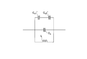
- FIG. 12 shows an equivalent circuit in which the capacitance components C s1 ′ and C s2 ′ are connected in parallel to the equivalent circuit of the low-frequency side bandpass resonator k Lb.
- the low-frequency side transmission frequency f Lb of the frequency selection plate 300 is a frequency to which the capacitance components C s1 ′ and C s2 ′ are added. Therefore, the low-frequency side transmission frequency f Lb can be controlled by changing the shape of the second conductive pattern forming the sub-resonator while keeping the shape of the low-frequency side bandpass resonator k Lb.
- the second conductive pattern F kHb1 forms a capacitance component C s1 ′ that is connected in parallel to the equivalent circuit of the high frequency side bandpass resonator k Hb .
- the high frequency side transmission frequency f Hb can be controlled by the second conductive pattern F kHb1 .
- the action is the same as in the case of the low-frequency side transmission frequency f Lb.
- the low frequency side band pass resonator k Lb and the high frequency side band pass resonator k Hb can be controlled independently. Therefore, by changing the shape of the second conductive pattern F KHb1 corresponding to the low frequency side band-pass resonators second conductive patterns F corresponding to the k Lb kLb1, F kLb2, and a high frequency band pass resonator k Hb, The bandwidth of the cutoff frequency can be controlled.
- the shape of the main resonator k xy is fixed, and a sub-resonator corresponding to the low-frequency side bandpass resonator k Lb and a sub-resonator corresponding to the high-frequency side bandpass resonator k Hb are respectively configured.
- the horizontal axis of FIG. 13 is the frequency [GHz], and the vertical axis is the reflection coefficient S 11 [dB] representing the reflection characteristic.
- the broken line indicates a characteristic example in which the low frequency side transmission frequency f Lb is lowered and the high frequency side transmission frequency f Hb is raised.
- the alternate long and short dash line shows a characteristic example in which the low-frequency side transmission frequency f Lb is increased and the high-frequency side transmission frequency f Hb is decreased.
- the cutoff frequency has not changed significantly.
- the cutoff frequency was changed by 3% or less. In this way, the bandwidth can be changed without changing the cutoff frequency.
- the second conductive patterns F kLb1 and F kLb2 and the second conductive pattern F kHb1 have been described in the example of being provided in the second conductive pattern, they may be provided in conductive patterns of different layers.
- the second conductive pattern F kHb1 may be formed as a third conductive pattern (not shown) arranged on the second conductive pattern F kLb1 and the like with a dielectric film interposed therebetween.
- a third conductive pattern (not shown) having the same shape may be formed so as to overlap the second conductive patterns F kLb1 and F kLb2 .
- the third conductive pattern having the same shape, it is possible to add a capacitive component in parallel to the parallel resonant circuit.
- the hook-shaped second conductive pattern F kHb1 may be formed with the third conductive pattern (not shown). By doing so, a sub-resonator that acts on the high-frequency bandpass resonator k Hb can be added.
- the frequency selection plate 300 includes the third conductive pattern disposed on the second conductive pattern with the dielectric film interposed therebetween, and the planar shape of the third conductive pattern is It has the same shape as the second conductive pattern, or a different shape from the second conductive pattern. As a result, the degree of freedom in designing the frequency selection plate 300 can be improved. Further, since a larger capacitance component can be added with the same planar shape, the frequency selection plate can be downsized.
- the thickness of the dielectric film 103 is within a range in which the capacitance component added by the second conductive pattern or the third conductive pattern can be treated as a concentrated constant.
- the distance between the conductive patterns may be about 0.125 mm. According to this, it is possible to ignore the transmission line-like propagation of electromagnetic waves in the thickness direction, and it is possible to facilitate the design of the frequency selection plates 200 and 300.
- the frequency selection plate 100 As described above, according to the frequency selection plate 100 according to the present embodiment, three resonance frequencies of the low frequency side transmission frequency f Lb and the high frequency side transmission frequency f Hb can be obtained with the cutoff frequency f Sb as the center. Each resonance frequency is determined by the corresponding parameter. Therefore, it is possible to provide a frequency selection plate in which the operating frequency and the bandwidth thereof can be easily adjusted.
- the sub-resonator corresponding to the main resonator k xy is provided.
- the operating frequency and its bandwidth can be adjusted by the conductive pattern forming the sub-resonator.
- the cutoff frequency bandwidth can be easily adjusted by adjusting the sub-resonator without changing the main resonator k xy .
- the frequency selection plate 300 includes sub-resonators corresponding to the low-frequency side bandpass resonator k Lb and the high-frequency side bandpass resonator k Hb .
- the operating frequency and its bandwidth can be adjusted by the conductive patterns forming the corresponding sub-resonators. Since the resonance frequency of the sub-resonator can be adjusted independently, it is easy to adjust the operating frequency and its bandwidth.
- the sub-resonator corresponding to the main resonator k xy , the sub-resonator corresponding to each of the low-frequency side bandpass resonator k Lb, and the high-frequency side bandpass resonator k Hb should be mounted on the same frequency selection plate. Is also possible.
- the planar shapes of the frequency selection plates shown in FIGS. 1, 7, and 11 are examples, and the shapes of the conductive patterns are not limited to these.
- the width of the conductive pattern joined to the pole plate portion of another adjacent resonator may be thinner or wider than the width shown in the figure.
- Frequency selection plate 103 Dielectric film 10: Horizontal pattern (conductor portion) 20: Vertical pattern (conductor part) 12, 12a, 12b; electrode plate portions 13, 13a, 13b: notch portion 14: conductive pattern (conductive pattern to be joined to electrode plate portions of other adjacent resonators)
- k xy resonator (main resonator)
- d Distance from the pole plate of another adjacent resonator
- D Distance across the diagonal of the tip of the pole plate
- l the length of the horizontal pattern and the vertical pattern
- w the width of the horizontal pattern and the vertical pattern
- h the length of the electrode plate portion 12 in the x direction (the height of the trapezoid)
- g widths F kLb1 , F kLb2 , F kHb1 of gaps between tip portions of
Landscapes
- Physics & Mathematics (AREA)
- Electromagnetism (AREA)
- Control Of Motors That Do Not Use Commutators (AREA)
- Aerials With Secondary Devices (AREA)
Abstract
動作周波数及びその帯域幅の調整が容易な周波数選択板を提供する。同一形状の導電パターンで形成される共振器kxyを、誘電体基板の上に周期的に配列した構造の周波数選択板において、共振器kxyは、誘電体基板101の上に十字を形成する横パターン10と縦パターン20の導線部と、横パターンと縦パターンが所定の長さ延伸されたそれぞれの両端部は、直交する方向にそれぞれ延長され、当該先端部分は他方向から延長された先端部分と対角線上に間隔を空けて対向する形状の極板部とを備え、極板部は、隣接する他の共振器の極板部と対向する中心部分が横パターンの幅で切り欠かれ、該切り欠かれた部分の中心から横パターン10の幅よりも細い幅で且つ所定の長さより短い長さ延伸されて隣接する他の共振器の極板部と接合し、先端部分の間隔は、隣接する他の共振器の極板部との間隔よりも広い形状である。
Description
本発明は、同一形状の共振器を、誘電体基板の上に周期的に配列した構造の周波数選択板に関する。
情報通信機器の小型化、高機能化が進み、無線LANやLTE等の回線を使った無線通信サービスが急速に普及している。これに伴い、無線通信端末からの電波の送受信が広域かつ頻繁に行われるようになり、周囲の他の電子機器への影響が懸念されている。
懸念される影響としては、無線環境の劣化、通信障害、及びセキュリティへの脅威などが考えられる。これらの影響を抑制する技術が求められている。
電波環境及び電磁環境を制御する目的で周波数選択板(FSS:Frequency Selective Surfaces)を用いることができる。周波数選択板は、波長と同程度以下の寸法の導体パターンで形成された共振器(単位セル)を周期的に配列することで、入射する電磁波の透過特性/反射特性に周波数依存性を持たせたものである。
周波数選択板には、様々な周波数特性を持つ共振構造が存在する。例えば、特定の周波数のみを反射するバンドストップフィルタ特性を持つものは、導体部を共振構造としたものが主であり、リング型、ダイポールアレイ型、トライホール型、パッチ型、及びエルサレムクロス型などがある(非特許文献1)。
周波数選択板は、考慮すべき構造パラメータの数が多く、パラメータがインダクタンス成分とキャパシタンス成分の増減に相反して関係する場合もある。また、単位セルの配列の仕方によってもその特性は変化し、理論として複雑である(非特許文献2)。
牧野 滋、「[チュートリアル講演]周波数選択板の基礎と応用」、信学技法、A・P 2015-5, Apl. 2015.
BEN A. MUNK,"Frequency Selective Surfaces Theory and Design",2000.
理論として複雑で有るが故に、一度の試作で所望の周波数特性を得ることが難しい。したがって、周波数選択板の設計は、コスト、労力を要するという課題がある。
本発明は、この課題に鑑みてなされたものであり、動作周波数及び帯域幅の調整が容易な周波数選択板を提供することを目的とする。
本発明の一態様に係る周波数選択板は、同一形状の導電パターンで形成される共振器を、誘電体基板の上に周期的に配列した構造の周波数選択板において、前記共振器は、前記誘電体基板の上に十字を形成する横パターンと縦パターンの導線部と、前記横パターンと前記縦パターンが所定の長さ延伸されたそれぞれの両端部は、直交する方向にそれぞれ延長され、延長された先端部分は他方向から延長された先端部分と対角線上に間隔を空けて対向する形状の極板部とを備え、極板部は、隣接する他の共振器の極板部と対向する中心部分が前記横パターンの幅で切り欠かれ、該切り欠かれた部分の中心から前記横パターンの幅よりも細い幅で且つ前記所定の長さより短い長さ延伸されて隣接する他の共振器の極板部と接合し、前記先端部分の間隔は、隣接する他の共振器の極板部との間隔よりも広い形状であることを要旨とする。
本発明によれば、動作周波数及びその帯域幅の調整が容易な周波数選択板を提供することができる。
以下、本発明の実施形態について図面を用いて説明する。複数の図面中同一のものには同じ参照符号を付し、説明は繰り返さない。
〔第1実施形態〕
図1は、本発明の第1実施形態に係る周波数選択板の一部の平面を模式的に示す図である。図1に示す周波数選択板100は、誘電体基板101の上に、漢字の「田」に似た形状の導電パターンで形成された共振器kxyが周期的に配列されて構成される。図1においてx方向を横、y方向を縦と定義する。
図1は、本発明の第1実施形態に係る周波数選択板の一部の平面を模式的に示す図である。図1に示す周波数選択板100は、誘電体基板101の上に、漢字の「田」に似た形状の導電パターンで形成された共振器kxyが周期的に配列されて構成される。図1においてx方向を横、y方向を縦と定義する。
誘電体基板101は、例えば、ガラスエポキシ基板、ポリミイドフィルム基板等で構成される。誘電体基板101の材質は、誘電体材料であれば何でも構わない。
誘電体基板101の上に導電膜102が形成される。所定の形状である共振器kxy(導電パターン)は、誘電体基板101の上に蒸着して形成しても良いし、誘電体基板101の表面全体に導電膜102を形成してからエッチングして形成しても良い。
共振器kxyは、例えば、x方向とy方向にそれぞれ10個並べられて周波数選択板100を構成する。1つの共振器kxyの大きさは、共振周波数の波長に対して1/3程度の大きさである。
信号は、周波数選択板100に対して-z方向(裏側)から入力され、z方向(表側)に出力(透過)される。周波数選択板100に電磁波が入力されると、共振器kxyが配列されたxy平面に電界が生じ共振現象による電流が流れる。
共振器kxyの構成を、+x方向で隣接する共振器k(x+1)yとの関係で説明する。
共振器kxyは、誘電体基板101の上に十字を形成する横パターン10と縦パターン20の導線部と、横パターン10と縦パターン20が所定の長さ延伸されたそれぞれの両端部は、直交する方向にそれぞれ延長(12a,12b)され、当該先端部分は他方向から延長された先端部分と対角線上に間隔Dを空けて対向する形状の極板部12とを備える。
そして、極板部12は、隣接する他の共振器k(x+1)yの極板部11と対向する中心部分が横パターン10の幅で切り欠かれ(切り欠き部13)、切り欠き部13の中心から横パターン10の幅よりも細い幅で且つ横パターン10の長さより短い長さ延伸されて隣接する他の共振器k(x+1)yの極板部11と接合する(導体パターン14)。横パターン10と直交する方向にそれぞれ延長された導体パターン12a,12bの先端部分の間隔Dは、隣接する他の共振器k(x+1)yの極板部11との間隔dよりも広い形状である。つまり、極板部12の平面形状は、外側を下底、内側を上底とする台形であり、下底の中心部分が切り欠かれ、その切り欠かれた切り欠き部13のy方向の中心から横パターン10よりも細い幅の導体パターン14が延伸され隣接する他の共振器k(x+1)yの極板部11と接合される形状である。切り欠き部13は、導体パターン14によって切り欠き部13a,13bの2つに分割される。
以上、共振器kxyの構成を+x方向で隣接する共振器k(x+1)yとの関係で説明したが、この構成は上下方向(y)及び左右方向(x)で同じである。つまり、各共振器kxyは、横パターン10の中心線で上下対称である。また、縦パターン20の中心線で左右対称である。
この特徴的な共振器kxyの構成により、本実施形態に係る周波数選択板100は、3つの共振電流が流れる共振パスを備える。
図2は、周波数選択板100に流れる3つの共振電流が流れる共振パスを模式的に示す図である。3つの共振電流は、直列共振周波数である遮断周波数(動作周波数)fSbの共振電流が流れるストップバンド経路Sb、低周波側の並列共振周波数(低周波側バンドパス周波数fLb)の共振電流が流れる低周波側バンドパス経路Lb、高周波側の並列共振周波数(高周波側バンドパス周波数fHb)の共振電流が流れる高周波側バンドパス経路Hbの3つである。
低周波側バンドパス経路Lbは、低周波側バンドパス共振器kLbを構成する。高周波側バンドパス経路Hbは、高周波側バンドパス共振器kHbを構成する。
ストップバンド経路Sbは、隣接する共振器kxyの横パターン10及び縦パターン20を通る経路である。図2では、図面が煩雑になることを理由に、x方向の+y側の経路のみを示している。実際のストップバンド経路Sbは、横パターン10を中心に-y方向に対称に存在する。また、縦パターン20を中心に±x方向にも存在する。
低周波側バンドパス経路Lbは、隣接する共振器kxyの切り欠き部13a同士の周りを周回する経路である。図2では、ストップバンド経路Sbと同様にx方向の+y側の経路のみを示している。実際の低周波側バンドパス経路Lbは、横パターン10を中心に-y方向に対称に存在する。また、縦パターン20を中心に±x方向にも存在する。
高周波側バンドパス経路Hbは、1つの共振器kxyの先端部分を対向させる極板部12aと21bを周回する経路である。高周波側バンドパス経路Hbは、上下及び左右対称の構成から、1つの共振器kxy内に4つ存在する。図2では、極板部12aと21bを周回する経路のみを示している。
図3は、各共振パスを構成する誘導成分と容量成分の共振器kxy上の部位を模式的に示す図である。誘導成分をL、容量成分をCで表記する。
図3(a)は、各成分を構成する部位の大凡の形状を破線で囲って示す図である。図3(b)は、各共振パスを等価回路で示す図である。
ストップバンド経路Sbは、横パターン10及び縦パターン20で形成される誘導成分L1、横パターン10と直交する方向の極板部12aで形成される誘導成分L2、及び極板部12aが隣接する共振器k(x+1)yの極板部11との間で形成される容量成分Csの直列接続で表せる(図3(b)に示す矢印の経路)。
低周波側バンドパス経路Lbは、切り欠き部13のx方向の間をつなぐ導体パターン14で形成される誘導成分L3が、誘導成分L2と容量成分Csの直列接続に並列に接続される経路で表せる(図3(b)に破線の円環で示す経路)。
高周波側バンドパス経路Hbは、導体パターン12a,21bの先端部分で形成される容量成分Cphと誘導成分L2の直列接続が、容量成分L1に並列に接続される経路で表せる(図3(b)に一点鎖線の円環で示す経路)。
図3(b)に示すZ0は、空間インピーダンスを表す。空間インピーダンスZ0は、真空の誘電率と透磁率から決まるインピーダンスである。
各経路で生じる共振周波数は、共振器kxyの形状を表すパラメータによって決定することができる。パラメータは主に、共振器kxyの形状を決定する各部の寸法である。
図4は、共振器kxyの形状を決定するパラメータの例を示す図である。導電パターンの厚さは1.3μmである。共振器kxyが周期的に配列されるピッチは10mmとした。
横パターン10及び縦パターン20の長さをl、横パターン10及び縦パターン20の幅をw、極板部12のx方向の長さをh(台形形状の高さ)、切り欠き部の幅をcx、切り欠き部の奥行きをcy、切り欠き部13内を橋渡す導電パターン14の幅をw2、及び極板部の先端部分の間隔Dの幅をgで表記している。
これらの寸法を決定すれば、導電パターン14の長さを含めて共振器kxyの形状が決定される。また、共振器kxyの形状を決定することで上記の誘導成分L1,L2、及び容量成分Cs,Cphの値が決定される。
図5は、図4に示す周波数選択板の共振周波数の解析結果を示す。図5の横軸は周波数[GHz]、縦軸は反射特性を表す反射係数S11[dB]である。解析した共振器kxyのパラメータは、l=6.8mm,d=0.2mm,g=0.8mm,w=1.5mm,w2=0.2mm,cx=1.5mm,cy=1.0mm,h=1.5mmとした。
図5に示すように遮断周波数fSbを中心に、低周波側透過周波数fLb、及び高周波側透過周波数fHbの3つの共振周波数が得られる。各共振周波数は、それぞれに対応するパラメータによって決定される。
遮断周波数fSbは、横パターン10及び縦パターン20で形成される誘導成分L1、横パターン10と直交する方向の極板部12aで形成される誘導成分L2、及び極板部12aが隣接する共振器k(x+1)yの極板部11aとの間で形成される容量成分Csによって決まる。よって、遮断周波数fSbは、パラメータの横パターン10及び縦パターン20の長さl、横パターン10及び縦パターン20の幅w、ピッチp、及び隣接する他の共振器の極板部との間隔dによって決定される。
図6は、容量成分Csによって遮断周波数fSbが変化する例を示す図である。図6の横軸は周波数[GHz]、縦軸は透過特性を表す透過係数S21[dB]である。破線は容量成分Csを大きくした場合であり、一点鎖線は容量成分Csを小さくした場合である。このように、例えば容量成分Csによって遮断周波数fSbを変化させることができる。
低周波側透過周波数fLbは、切り欠き部13内を橋渡しする導電パターン14の幅w2とピッチpによる誘導成分L3と、誘導成分L2と容量成分Csとによって決まる。誘導成分L2と容量成分Csは、遮断周波数fSbを決定するパラメータでもある。したがって、低周波側透過周波数fLbは、主に導電パターン14の幅w2で制御することができる。
高周波側透過周波数fHbは、導体パターン12a,21bの先端部分で形成される容量成分Cphと誘導成分L2によって決まる。誘導成分L2は、遮断周波数fSbを決定するパラメータでもある。したがって、高周波側透過周波数fHbは、主に導体パターン12a,21bの先端部分で形成される容量成分Cphで制御することができる。
このように3つの共振器の共振周波数は、それぞれ独立させて制御することが可能である。つまり、動作周波数及びその帯域幅の調整が容易である。
以上説明したように本実施形態に係る周波数選択板100は、同一形状の導電パターンで形成される共振器kxyを、誘電体基板101の上に周期的に配列した構造の周波数選択板100において、共振器kxyは、誘電体基板101の上に十字を形成する横パターン10と縦パターン20の導線部と、横パターン10と縦パターン20が所定の長さ延伸されたそれぞれの両端部は、直交する方向にそれぞれ延長され、当該先端部分は他方向から延長された先端部分と対角線上に間隔を空けて対向する形状の極板部12とを備え、極板部12は、隣接する他の共振器の極板部11と対向する中心部分が横パターン10の幅で切り欠かれ、該切り欠かれた部分13の中心から横パターン10の幅よりも細い幅で且つ所定の長さより短い長さ延伸されて隣接する他の共振器の極板部11と接合し、極板部の先端部分の間隔Dは、隣接する他の共振器の極板部との間隔dよりも広い形状である。これにより動作周波数及びその帯域幅の調整を容易にすることができる。
本実施形態に係る周波数選択板100は、遮断周波数fSbを中心に、低周波側透過周波数fLb、及び高周波側透過周波数fHbを備えるので、低周波側透過周波数fLbと高周波側透過周波数fHbを遮断周波数fSbに近づけることで遮断特性(バンドストップ特性)を狭帯域化することもできる。
〔第2実施形態〕
図7は、本発明の第2実施形態に係る周波数選択板の平面図を模式的に示す図である。図6に示す周波数選択板200は、副共振器を備える点で周波数選択板100(図1)と異なる。
図7は、本発明の第2実施形態に係る周波数選択板の平面図を模式的に示す図である。図6に示す周波数選択板200は、副共振器を備える点で周波数選択板100(図1)と異なる。
図7に示す周波数選択板200の副共振器は、隣接する極板部12aと11aの先端部分を覆う例えばホームベース形状の第2導電パターンFkpで構成される。y方向の極板部21,22の先端部分にも第2導電パターンFkpが形成される。
第2導電パターンFkpは、極板部12a等の導電膜102と誘電体層を挟んで重ね合わせて形成される。導電パターンFkpを、層状に重ね合わせる方法としては、例えば共振器kxyと導電パターンFkpが形成されたフレキシブル基板又はリジッド基板を2つ重ねて実装する方法や、PET基板に印刷された2枚の導電パターンをラミネート加工によって重ね合わせた状態で固定する方法などが考えられる。又は、蒸着膜及び拡散膜を形成する半導体プロセスを用いて作製してもよい。
図8は、副共振器の構造を模式的に示す図である。図7(a)はその斜視図である。図8(b)は図8(a)に示すA-A線で切った断面図である。
図8(a)に示すように、隣接する極板部12aと11aに、誘電体層を挟んで重ねられた導電パターンFkpによって、2つの容量成分Cs′の直列接続が、隣接する極板部12a,11aで形成される容量成分Csに並列に接続される。
図8(b)に示すように、容量成分Cs′は、誘電体基板101、導電膜102、誘電体膜103、及び第2導電パターン104の4層で構成される。なお、更に誘電体膜と導電膜を増やしても良い。詳しくは後述する。
図9は、副共振器を備える周波数選択板200の等価回路を模式的に示す図である。導電膜102で形成される共振器kxy(以降、主共振器と称する場合がある)の等価回路は、誘導成分Lと容量成分Csの直列接続で表現している。
よって、周波数選択板200は、主共振器kxyの容量成分Csに、2つの容量成分Cs′の直列接続が並列に接続された等価回路で表せる。第2導電パターンFkpと極板部12a,11aの間に形成される容量は、極板部12a,11a同士の間で形成されう容量成分Csよりも大きい(Cs′≫Cs)。
図9に示す等価回路から明らかなように、本実施形態に係る周波数選択板200の遮断周波数は、容量成分Cs′が付加された周波数である。したがって、主共振器kxyの形状はそのままにし、副共振器を形成する第2導電パターンの形状を変えることで、遮断周波数を制御することができる。
図10は、第2導電パターンFkpの形状を変えた場合の遮断周波数の変化を示す図である。
図10(a)はx方向の長さを変えた場合の変化を示す図であり、図10(b)はy方向の長さを変えた場合の変化を示す図である。図10の横軸は周波数[GHz]、縦軸は透過特性を表す透過係数S21[dB]である。
図10(a)のパラメータ0mmは、図6に示す第2導電パターンFkpの形状の場合である。パラメータ0.2mmは、第2導電パターンFkpの幅を-0.2mmしたことを表す。つまり、一方の極板部12aの外側から-0.1mm、他方の極板部11aの外側から-0.1mmした場合の特性である。
図10(a)に示すように、第2導電パターンFkpの幅を0~1mmの範囲で変えることで遮断周波数を約1GHzの範囲で可変することができる。つまり、主共振器kxyの形状を変えずに第2導電パターンFkpの形状を変えることで遮断周波数を調整することができる。
図10(b)のパラメータ0mm~0.5mmは、第2導電パターンFkpのy方向の長さを変化させた寸法を表す。パラメータ0mmは、図6に示す第2導電パターンFkpの形状の場合である。
図10(b)に示すように、第2導電パターンFkpのy方向の長さを0~0.5mmの範囲で変えることで遮断周波数を約0.5GHzの範囲で可変することができる。このように第2導電パターンFkpのy方向の長さを変えても遮断周波数を調整することができる。
以上説明したように、本実施形態に係る周波数選択板200は、導線部の上に誘電体膜を挟んで配置される第2導電パターンを備え、第2導電パターンの平面形状は、隣接する共振器同士で同一部分を覆う形状、及び同一の共振器の極板部の間を覆う形状である。これにより、主共振器kxyの形状を変えずにその遮断周波数を調整することができる。
〔第3実施形態〕
図11は、本発明の第3実施形態に係る周波数選択板の平面図を模式的に示す図である。図11に示す周波数選択板300は、周波数選択板100(図1)に対して低周波側バンドパス共振器kLbと高周波側バンドパス共振器kHbのそれぞれに対応する副共振器を備えたものである。
図11は、本発明の第3実施形態に係る周波数選択板の平面図を模式的に示す図である。図11に示す周波数選択板300は、周波数選択板100(図1)に対して低周波側バンドパス共振器kLbと高周波側バンドパス共振器kHbのそれぞれに対応する副共振器を備えたものである。
低周波側バンドパス共振器kLbに対応する副共振器は、この例では2つの第2導電パターンFkLb1とFkLb2で構成される。第2導電パターンFkLb1,FkLb2は、第2導電パターンFkpと同様に、極板部12a等の導電膜102と誘電体層を挟んで重ね合わせて形成される。
第2導電パターンFkLb1,FkLb2のそれぞれは、容量成分Cs1′とCs2′を形成させる。第2導電パターンFkLb1,FkLb2は、隣接する共振器を跨いで同じ形状である。つまり、極板板12aの上の形状と、極板板11aの上のそれぞれの第2導電パターンFkLb1形状は同じであり、隣接する共振器の間で繋がっている。容量成分Cs1′とCs2′は、低周波側バンドパス共振器kLbの並列共振周波数に並列に接続されて作用する。
図12は、容量成分Cs1′とCs2′が、低周波側バンドパス共振器kLbの等価回路に並列に接続された等価回路を示す。この等価回路から明らかなように、本実施形態に係る周波数選択板300の低周波側透過周波数fLbは、容量成分Cs1′とCs2′が付加された周波数である。したがって、低周波側バンドパス共振器kLbの形状はそのままにし、副共振器を形成する第2導電パターンの形状を変えることで、低周波側透過周波数fLbを制御することができる。
第2導電パターンFkHb1は、高周波側バンドパス共振器kHbの等価回路に並列に接続される容量成分Cs1′を形成する。第2導電パターンFkHb1によって高周波側透過周波数fHbを制御することができる。その作用は、低周波側透過周波数fLbの場合と同じである。
低周波側バンドパス共振器kLbと高周波側バンドパス共振器kHbは、それぞれ独立させて制御することができる。よって、低周波側バンドパス共振器kLbに対応する第2導電パターンFkLb1,FkLb2、及び高周波側バンドパス共振器kHbに対応する第2導電パターンFkHb1の形状を変化させることで、遮断周波数の帯域幅を制御することができる。
図13は、主共振器kxyの形状を固定し、低周波側バンドパス共振器kLbに対応する副共振器と高周波側バンドパス共振器kHbに対応する副共振器をそれぞれ構成する第2導電パターンFkLb1,FkLb2,FkHb1の形状を変えた場合の反射特性の例を示す図である。
図13の横軸は周波数[GHz]、縦軸は反射特性を表す反射係数S11[dB]である。
図13において、破線は、低周波側透過周波数fLbを下げ、高周波側透過周波数fHbを上げた特性例を示す。一点鎖線は、低周波側透過周波数fLbを上げ、高周波側透過周波数fHbを下げた特性例を示す。このように低周波側バンドパス共振器kLbと高周波側バンドパス共振器kHbにそれぞれ対応する副共振器を構成する第2導電パターンFkLb1,FkLb2,FkHb1の形状を変えることで周波数選択板300の帯域幅を制御することができる。
ここで注目すべきは、遮断周波数が大きく変化していない点である。図13に示す例では、遮断周波数は3%以下の変化であった。このように遮断周波数を変化させずに帯域幅を可変することができる。
第2導電パターンFkLb1,FkLb2と第2導電パターンFkHb1は、何れも第2導電パターンに設ける例で説明したが、両者は異なる層の導電パターンに設けるようにしても良い。例えば、第2導電パターンFkHb1を、第2導電パターンFkLb1等の上に誘電体膜を挟んで配置される第3導電パターン(図示せず)で形成するようにしても良い。
また、第2導電パターンFkLb1,FkLb2と重なるように同じ形状の第3導電パターン(図示せず)を形成するようにしても良い。同じ形状の第3導電パターンによって、並列共振回路に更に並列に容量成分を付加することができる。
また、図11において鈎形状の第2導電パターンFkHb1を、第3導電パターン(図示せず)を形成するようにしても良い。そうすることで、高周波側バンドパス共振器kHbに作用する副共振器を付加することができる。
このように本発明の第3実施形態に係る周波数選択板300は、第2導電パターンの上に誘電体膜を挟んで配置される第3導電パターンを備え、第3導電パターンの平面形状は、第2導電パターンと同形状である、又は第2導電パターンと異なる形状である。これにより、周波数選択板300の設計の自由度を向上させることができる。また、同じ平面形状でより大きな容量成分を付加することができるので、周波数選択板を小型化することができる。
なお、誘電体膜103(図8(b))の厚さは、第2導電パターン又は第3導電パターンによって付加される容量成分が集中常数で扱える範囲の厚さである。例えば、共振器kxyを、誘電体基板101の上に周期的に配列するピッチを10mmとした場合は、導電パターンの間の間隔を0.125mm程度にすると良い。これによれば、厚さ方向における電磁波の伝送線路的な伝搬を無視することができ、周波数選択板200,300の設計を容易にすることができる。
以上説明したように本実施形態に係る周波数選択板100によれば、遮断周波数fSbを中心に、低周波側透過周波数fLb、及び高周波側透過周波数fHbの3つの共振周波数が得られる。各共振周波数は、それぞれに対応するパラメータによって決定される。したがって、動作周波数及びその帯域幅の調整が容易な周波数選択板を提供することができる。
また、周波数選択板200によれば、主共振器kxyに対応する副共振器を備える。副共振器を構成する導電パターンによって、動作周波数及びその帯域幅の調整が行える。主共振器kxyを変更せずに副共振器を調整することで遮断周波数の帯域幅を容易に調整できる。
また、周波数選択板300によれば、低周波側バンドパス共振器kLbと高周波側バンドパス共振器kHbのそれぞれに対応する副共振器を備える。それぞれに対応する副共振器を構成する導電パターンによって、動作周波数及びその帯域幅の調整が行える。副共振器の共振周波数は独立して調整できるので動作周波数及びその帯域幅の調整が容易である。
なお、主共振器kxyに対応する副共振器と低周波側バンドパス共振器kLbと高周波側バンドパス共振器kHbのそれぞれに対応する副共振器を、同じ周波数選択板に実装することも可能である。また、図1、図7、及び図11にそれぞれ示した周波数選択板の平面形状は、一例であり導電パターンの形状はこれらに限定されない。例えば、隣接する他の共振器の極板部と接合する導電パターンの幅は、図に示す幅よりも細くても良いし、太くても良い。このように、本発明はここでは記載していない様々な実施形態等を含むことは勿論である。したがって、本発明の技術的範囲は上記の説明から妥当な特許請求の範囲に係る発明特定事項によってのみ定められるものである。
100,200,300:周波数選択板
103:誘電体膜
10:横パターン(導線部)
20:縦パターン(導線部)
12,12a,12b;極板部
13,13a,13b:切り欠き部
14:導電パターン(隣接する他の共振器の極板部と接合する導電パターン)
kxy:共振器(主共振器)
d:隣接する他の共振器の極板部との間隔
D:極板部の先端部分の対角線を挟んだ間隔
l:横パターン及び縦パターンの長さ
w:横パターン及び縦パターンの幅
h:極板部12のx方向の長さ(台形の高さ)
cx:切り欠き部の幅
cy:切り欠き部の奥行き
w2:切り欠き部内を橋渡す導電パターンの幅
g:極板部の先端部分の間隔の幅
FkLb1,FkLb2,FkHb1:第2導電パターン
103:誘電体膜
10:横パターン(導線部)
20:縦パターン(導線部)
12,12a,12b;極板部
13,13a,13b:切り欠き部
14:導電パターン(隣接する他の共振器の極板部と接合する導電パターン)
kxy:共振器(主共振器)
d:隣接する他の共振器の極板部との間隔
D:極板部の先端部分の対角線を挟んだ間隔
l:横パターン及び縦パターンの長さ
w:横パターン及び縦パターンの幅
h:極板部12のx方向の長さ(台形の高さ)
cx:切り欠き部の幅
cy:切り欠き部の奥行き
w2:切り欠き部内を橋渡す導電パターンの幅
g:極板部の先端部分の間隔の幅
FkLb1,FkLb2,FkHb1:第2導電パターン
Claims (4)
- 同一形状の導電パターンで形成される共振器を、誘電体基板の上に周期的に配列した構造の周波数選択板において、
前記共振器は、
前記誘電体基板の上に十字を形成する横パターンと縦パターンの導線部と、
前記横パターンと前記縦パターンが所定の長さ延伸されたそれぞれの両端部は、直交する方向にそれぞれ延長され、延長された先端部分は他方向から延長された先端部分と対角線上に間隔を空けて対向する形状の極板部と
を備え、
極板部は、隣接する他の共振器の極板部と対向する中心部分が前記横パターンの幅で切り欠かれ、該切り欠かれた部分の中心から前記横パターンの幅よりも細い幅で且つ前記所定の長さより短い長さ延伸されて隣接する他の共振器の極板部と接合し、前記先端部分の間隔は、隣接する他の共振器の極板部との間隔よりも広い形状である
ことを特徴とする周波数選択板。 - 前記導電パターンの上に誘電体膜を挟んで配置される第2導電パターンを備え、
第2導電パターンの平面形状は、隣接する共振器同士の同一部分を覆う形状、及び同一の共振器の前記極板部の間を覆う形状である
ことを特徴とする請求項1に記載の周波数選択板。 - 第2導電パターンの上に誘電体膜を挟んで配置される第3導電パターンを備え、
第3導電パターンの平面形状は、第2導電パターンと同形状である、又は第2導電パタ-ンと異なる形状である
ことを特徴とする請求項2に記載の周波数選択板。 - 前記誘電体膜の厚さは、第2導電パターン又は第3導電パターンによって付加される容量成分が集中定数で扱える範囲の厚さである
ことを特徴とする請求項3に記載の周波数選択板。
Priority Applications (1)
| Application Number | Priority Date | Filing Date | Title |
|---|---|---|---|
| US17/414,475 US11715883B2 (en) | 2018-12-25 | 2019-12-11 | Frequency selective surface |
Applications Claiming Priority (2)
| Application Number | Priority Date | Filing Date | Title |
|---|---|---|---|
| JP2018240590A JP6959537B2 (ja) | 2018-12-25 | 2018-12-25 | 周波数選択板 |
| JP2018-240590 | 2018-12-25 |
Publications (1)
| Publication Number | Publication Date |
|---|---|
| WO2020137540A1 true WO2020137540A1 (ja) | 2020-07-02 |
Family
ID=71125843
Family Applications (1)
| Application Number | Title | Priority Date | Filing Date |
|---|---|---|---|
| PCT/JP2019/048427 Ceased WO2020137540A1 (ja) | 2018-12-25 | 2019-12-11 | 周波数選択板 |
Country Status (3)
| Country | Link |
|---|---|
| US (1) | US11715883B2 (ja) |
| JP (1) | JP6959537B2 (ja) |
| WO (1) | WO2020137540A1 (ja) |
Cited By (1)
| Publication number | Priority date | Publication date | Assignee | Title |
|---|---|---|---|---|
| WO2025027966A1 (ja) * | 2023-08-01 | 2025-02-06 | Toppanホールディングス株式会社 | 電磁波反射板および電磁波反射装置 |
Families Citing this family (3)
| Publication number | Priority date | Publication date | Assignee | Title |
|---|---|---|---|---|
| CN113631426B (zh) | 2019-03-29 | 2024-09-17 | 株式会社自动网络技术研究所 | 布线模块 |
| US11831073B2 (en) * | 2020-07-17 | 2023-11-28 | Synergy Microwave Corporation | Broadband metamaterial enabled electromagnetic absorbers and polarization converters |
| CN113346250B (zh) * | 2021-06-22 | 2022-09-16 | 重庆邮电大学 | 一种基于多层耦合结构的毫米波三频频率选择表面 |
Citations (3)
| Publication number | Priority date | Publication date | Assignee | Title |
|---|---|---|---|---|
| US20070159395A1 (en) * | 2006-01-06 | 2007-07-12 | Sievenpiper Daniel F | Method for fabricating antenna structures having adjustable radiation characteristics |
| JP2008252046A (ja) * | 2007-03-30 | 2008-10-16 | Fujimori Kogyo Co Ltd | 周波数選択遮蔽型の電磁波シールド積層体 |
| JP2018191247A (ja) * | 2017-05-11 | 2018-11-29 | 日本電信電話株式会社 | 電磁界バンドパスフィルタ |
Family Cites Families (8)
| Publication number | Priority date | Publication date | Assignee | Title |
|---|---|---|---|---|
| US5917458A (en) * | 1995-09-08 | 1999-06-29 | The United States Of America As Represented By The Secretary Of The Navy | Frequency selective surface integrated antenna system |
| JP2007235460A (ja) * | 2006-02-28 | 2007-09-13 | Mitsumi Electric Co Ltd | アンテナ装置 |
| US7639206B2 (en) * | 2008-05-05 | 2009-12-29 | University Of Central Florida Research Foundation, Inc. | Low-profile frequency selective surface based device and methods of making the same |
| US8786507B2 (en) * | 2011-04-27 | 2014-07-22 | Blackberry Limited | Antenna assembly utilizing metal-dielectric structures |
| KR102175681B1 (ko) * | 2014-11-20 | 2020-11-06 | 삼성전자주식회사 | 재방사 중계기 |
| US9748642B2 (en) * | 2014-12-22 | 2017-08-29 | The Charles Stark Draper Laboratory, Inc. | Low-profile loop antenna |
| US11616299B2 (en) * | 2018-12-19 | 2023-03-28 | The Regents Of The University Of California | Nonreciprocal reflectarray antennas based on time-modulated unit-cells |
| US11133588B1 (en) * | 2021-03-08 | 2021-09-28 | The Florida International University Board Of Trustees | Phase change material based reconfigurable intelligent reflective surfaces |
-
2018
- 2018-12-25 JP JP2018240590A patent/JP6959537B2/ja active Active
-
2019
- 2019-12-11 WO PCT/JP2019/048427 patent/WO2020137540A1/ja not_active Ceased
- 2019-12-11 US US17/414,475 patent/US11715883B2/en active Active
Patent Citations (3)
| Publication number | Priority date | Publication date | Assignee | Title |
|---|---|---|---|---|
| US20070159395A1 (en) * | 2006-01-06 | 2007-07-12 | Sievenpiper Daniel F | Method for fabricating antenna structures having adjustable radiation characteristics |
| JP2008252046A (ja) * | 2007-03-30 | 2008-10-16 | Fujimori Kogyo Co Ltd | 周波数選択遮蔽型の電磁波シールド積層体 |
| JP2018191247A (ja) * | 2017-05-11 | 2018-11-29 | 日本電信電話株式会社 | 電磁界バンドパスフィルタ |
Non-Patent Citations (1)
| Title |
|---|
| HOSSEINIPANAH ET AL.: "Novel Frequency Selective Surfaces Designing by Modification of Jerusalem Cross Slot", ICMMT 2008, vol. 2008, pages 1 - 4, XP031270402 * |
Cited By (1)
| Publication number | Priority date | Publication date | Assignee | Title |
|---|---|---|---|---|
| WO2025027966A1 (ja) * | 2023-08-01 | 2025-02-06 | Toppanホールディングス株式会社 | 電磁波反射板および電磁波反射装置 |
Also Published As
| Publication number | Publication date |
|---|---|
| JP6959537B2 (ja) | 2021-11-02 |
| US20220077590A1 (en) | 2022-03-10 |
| US11715883B2 (en) | 2023-08-01 |
| JP2020102801A (ja) | 2020-07-02 |
Similar Documents
| Publication | Publication Date | Title |
|---|---|---|
| WO2020137540A1 (ja) | 周波数選択板 | |
| US11081767B2 (en) | Multilayered filter device | |
| CN106410336A (zh) | 一种堆叠式三阶基片集成波导滤波器 | |
| CN114976619A (zh) | 一种基于多耦合贴片结构的双极化滤波天线 | |
| KR102444699B1 (ko) | 도파관 슬롯 안테나 | |
| CN108028634A (zh) | 层叠带通滤波器 | |
| CN113497351B (zh) | 滤波天线及无线通信设备 | |
| WO2014192784A1 (ja) | Ebg構造 | |
| JP3901130B2 (ja) | 共振器、フィルタおよび通信装置 | |
| WO2021009893A1 (ja) | 周波数選択板 | |
| JP2000013106A (ja) | 誘電体フィルタ、送受共用器および通信装置 | |
| JP4693587B2 (ja) | バンドパスフィルタ | |
| KR20150112891A (ko) | 슬롯 라인 공진기를 구비한 필터링 회로 | |
| JP6974738B2 (ja) | 周波数選択板 | |
| JP2019134326A (ja) | 誘電体フィルタ | |
| CN119994424B (zh) | 一种贴片腔体滤波器 | |
| JP2007089000A (ja) | ストリップラインフィルタ | |
| JP2010239461A (ja) | デュアルモード・バンドパスフィルタ | |
| JP7255997B2 (ja) | 導波管スロットアンテナ | |
| JPH10224044A (ja) | フィルタ実装多層基板 | |
| JP2020529798A (ja) | 導波管アンテナ磁気電気的適合変換器 | |
| WO2025225106A1 (ja) | 多層基板アンテナ及び電子機器 | |
| JP2006238195A (ja) | 積層型誘電体フィルタ | |
| WO2004114455A1 (ja) | 共振器、フィルタおよび通信装置 | |
| JP2021136624A (ja) | アンテナ素子及びアレイアンテナ |
Legal Events
| Date | Code | Title | Description |
|---|---|---|---|
| 121 | Ep: the epo has been informed by wipo that ep was designated in this application |
Ref document number: 19905303 Country of ref document: EP Kind code of ref document: A1 |
|
| NENP | Non-entry into the national phase |
Ref country code: DE |
|
| 122 | Ep: pct application non-entry in european phase |
Ref document number: 19905303 Country of ref document: EP Kind code of ref document: A1 |