WO2020136876A1 - 弾性波変調素子及び物理量センサ - Google Patents
弾性波変調素子及び物理量センサ Download PDFInfo
- Publication number
- WO2020136876A1 WO2020136876A1 PCT/JP2018/048486 JP2018048486W WO2020136876A1 WO 2020136876 A1 WO2020136876 A1 WO 2020136876A1 JP 2018048486 W JP2018048486 W JP 2018048486W WO 2020136876 A1 WO2020136876 A1 WO 2020136876A1
- Authority
- WO
- WIPO (PCT)
- Prior art keywords
- magnetic flux
- piezoelectric member
- elastic wave
- pair
- main surface
- Prior art date
- Legal status (The legal status is an assumption and is not a legal conclusion. Google has not performed a legal analysis and makes no representation as to the accuracy of the status listed.)
- Ceased
Links
Images



Classifications
-
- G—PHYSICS
- G01—MEASURING; TESTING
- G01K—MEASURING TEMPERATURE; MEASURING QUANTITY OF HEAT; THERMALLY-SENSITIVE ELEMENTS NOT OTHERWISE PROVIDED FOR
- G01K7/00—Measuring temperature based on the use of electric or magnetic elements directly sensitive to heat ; Power supply therefor, e.g. using thermoelectric elements
- G01K7/32—Measuring temperature based on the use of electric or magnetic elements directly sensitive to heat ; Power supply therefor, e.g. using thermoelectric elements using change of resonant frequency of a crystal
-
- G—PHYSICS
- G01—MEASURING; TESTING
- G01L—MEASURING FORCE, STRESS, TORQUE, WORK, MECHANICAL POWER, MECHANICAL EFFICIENCY, OR FLUID PRESSURE
- G01L1/00—Measuring force or stress, in general
-
- G—PHYSICS
- G01—MEASURING; TESTING
- G01R—MEASURING ELECTRIC VARIABLES; MEASURING MAGNETIC VARIABLES
- G01R33/00—Arrangements or instruments for measuring magnetic variables
- G01R33/02—Measuring direction or magnitude of magnetic fields or magnetic flux
-
- H—ELECTRICITY
- H03—ELECTRONIC CIRCUITRY
- H03B—GENERATION OF OSCILLATIONS, DIRECTLY OR BY FREQUENCY-CHANGING, BY CIRCUITS EMPLOYING ACTIVE ELEMENTS WHICH OPERATE IN A NON-SWITCHING MANNER; GENERATION OF NOISE BY SUCH CIRCUITS
- H03B5/00—Generation of oscillations using amplifier with regenerative feedback from output to input
- H03B5/30—Generation of oscillations using amplifier with regenerative feedback from output to input with frequency-determining element being electromechanical resonator
-
- H—ELECTRICITY
- H03—ELECTRONIC CIRCUITRY
- H03H—IMPEDANCE NETWORKS, e.g. RESONANT CIRCUITS; RESONATORS
- H03H9/00—Networks comprising electromechanical or electro-acoustic elements; Electromechanical resonators
- H03H9/02—Details
- H03H9/125—Driving means, e.g. electrodes, coils
- H03H9/145—Driving means, e.g. electrodes, coils for networks using surface acoustic waves
Definitions
- the present invention relates to an elastic wave modulator and a physical quantity sensor, and more particularly to an elastic wave modulator capable of detecting a physical quantity of an object to be detected based on a change in propagation characteristics of surface acoustic waves.
- delay line type and resonator type sensors using surface acoustic waves (hereinafter, also referred to as SAW (Surface Acoustic Wave)).
- SAW Surface Acoustic Wave
- a structure of the delay line type SAW sensor for example, a LiNbO 3 substrate, a pair of comb-teeth electrode portions provided on the substrate, and an amorphous material arranged in the SAW propagation region between the pair of comb-teeth electrode portions are used.
- a SAW delay line including a TbFe 2 film has been proposed (Non-Patent Document 1).
- a transponder having a surface acoustic wave element having a piezoelectric substrate and a comb-teeth electrode and an antenna means, a drive signal is transmitted to the transponder, and a response from the transponder.
- a wireless SAW sensor consisting of an interrogator that receives a signal has been proposed.
- This SAW sensor has a magnetostrictive film having a substantially rectangular shape having sides that match the propagation direction of surface acoustic waves, and is provided with a magnetostrictive film that is separated from the comb-tooth electrode.
- the stress acting on the piezoelectric substrate is detected based on the time difference between the echo corresponding to the reflected wave from the echo and the echo corresponding to the reflected wave from the end portion of the rectangular magnetostrictive film on the side opposite to the comb-teeth electrode (Patent Document 1). ).
- the so-called ⁇ E effect of the magnetostrictive film depends on the change of the magnetization state in the magnetostrictive film, the ⁇ E effect is unlikely to occur when the change amount of the magnetization state is small. Therefore, when the stress acting on the piezoelectric substrate is small, the stress acting on the piezoelectric substrate cannot be sufficiently detected, and the sensitivity may not be good.
- the external magnetic field (magnetic field) applied to the magnetostrictive film is small, the amount of change in the magnetization state due to the external magnetic field is small, so the ⁇ E effect is also small, and the magnetic field sensitivity as a sensor may not be good.
- An object of the present invention is to provide an elastic wave modulation element and a physical quantity sensor capable of improving the sensitivity as compared with the prior art and detecting the physical quantity of a detected object with high accuracy.
- the present invention provides the following means.
- a piezoelectric member A first electrode portion attached to the piezoelectric member for exciting elastic waves in the piezoelectric member;
- a magnetostrictive material portion provided in the region where the elastic wave exists or in the vicinity thereof, Equipped with The magnetostrictive material portion,
- a pair of magnetic flux propagating portions provided on one of the main surfaces of the piezoelectric member and capable of propagating the magnetic flux of the external magnetic field, Provided between the pair of magnetic flux propagating portions on the one main surface, and having a magnetism collecting portion arranged on the propagation path of the elastic wave or in the vicinity thereof,
- the thickness of the side surface of the magnetic flux collecting portion facing the magnetic flux propagating portion is smaller than the thickness of the side surface of the magnetic flux propagating portion facing the magnetic flux collecting portion,
- An elastic wave modulator characterized by the above.
- Each of the pair of magnetic flux propagating portions has a shape in which a cross-sectional area decreases along a direction from one end portion on the side opposite to the magnetic flux collecting portion to the other end portion on the magnetic flux collecting portion side.
- the magnetic flux in the magnetism collecting portion is formed along a direction perpendicular to the propagation direction of the elastic wave,
- the pair of magnetic flux propagating portions and the magnetic flux collecting portion are arranged on one main surface of the piezoelectric member,
- the magnetic flux in the magnetism collecting portion is formed along the propagation direction of the elastic wave,
- the pair of magnetic flux propagating portions and the magnetic flux collecting portion are arranged on one main surface of the piezoelectric member,
- the first electrode portion and the second electrode portion are arranged on the one main surface at positions corresponding to a pair of openings provided in the pair of magnetic flux propagating portions, or on the one main surface.
- the elastic wave modulation element according to the above [3] which is arranged on a surface and below the pair of magnetic flux propagating portions, or arranged on the other main surface of the piezoelectric member.
- the magnetism collecting part is arranged at a position including the first electrode part and the second electrode part on a projection surface projected in the thickness direction of the piezoelectric member, [1] or [2].
- the magnetic flux in the magnetism collecting portion is formed along a direction perpendicular to the propagation direction of the elastic wave,
- the pair of magnetic flux propagating portions and the magnetic flux collecting portion are arranged on one main surface of the piezoelectric member,
- the first electrode portion and the second electrode portion are arranged on the one main surface of the piezoelectric member and below the magnetism collecting portion, or on the other main surface of the piezoelectric member.
- the magnetic flux in the magnetism collecting portion is formed along the propagation direction of the elastic wave,
- the pair of magnetic flux propagating portions and the magnetic flux collecting portion are arranged on one main surface of the piezoelectric member,
- the first electrode portion and the second electrode portion are arranged on the one main surface of the piezoelectric member and below the magnetism collecting portion, or on the other main surface of the piezoelectric member.
- the elastic wave modulator according to the above [6] which is arranged.
- the first electrode portion is composed of a pair of comb-teeth electrodes arranged so as to face each other so that the teeth are alternately arranged
- the elastic wave according to any one of the above [1] to [8], wherein the second electrode portion is configured by another pair of comb-teeth electrodes arranged so as to face each other so that the teeth are alternately arranged.
- Modulation element [10] The elasticity according to any one of the above [1] to [8], wherein the first electrode portion and the second electrode portion are a pair of comb-teeth electrodes for exciting or receiving elastic waves in the piezoelectric member. Wave modulator.
- [11] Further includes one reflector attached to the piezoelectric member and arranged on one side of the magnetism collecting unit, The first electrode portion and the second electrode portion are arranged on one main surface of the piezoelectric member and on the other side of the magnetism collecting portion, or on one main surface of the piezoelectric member.
- the elastic wave modulator according to any one of [1] to [10] above, which is disposed under the magnetic flux collector.
- the magnetism collecting unit is arranged at a position including the one reflector on a projection plane projected in the thickness direction of the piezoelectric member, and the one reflector is the one main member of the piezoelectric member.
- the magnetism collecting portion is arranged at a position that includes the pair of reflectors on a projection surface projected in the thickness direction of the piezoelectric member, and the pair of reflectors is the main one of the piezoelectric members.
- the elastic wave modulation element according to the above [13] which is arranged on a surface and below the magnetic flux collector.
- the cross-sectional area of the end of the magnetic flux collecting portion on the side facing the magnetic flux propagating portion is larger than the cross-sectional area of the end of the magnetic flux collecting portion on the side facing the magnetic flux collecting portion. 1] to the elastic wave modulator according to any one of [14]. [16] A physical quantity sensor including the elastic wave modulation element according to any one of [1] to [15] above, and a circuit unit that detects modulation of the elastic wave modulation element.
- the present invention it is possible to improve the sensitivity as compared with the related art and to accurately detect the physical quantity of the detected object.
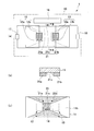
- FIG. 3A and 3B are diagrams schematically showing a configuration of a physical quantity sensor including the elastic wave modulation element according to the first embodiment of the present invention, where FIG. 1A is a plan view, FIG. 2B is a sectional view taken along line II, and FIG. ) Is a bottom view.
- FIG. 1A is a plan view
- FIG. 2B is a sectional view taken along line II
- FIG. ) Is a bottom view.
- (A) is a figure which shows the 1st modification of the elastic wave modulator in FIG. 1
- (b) is a figure which shows a 2nd modification.
- FIG. 1 It is a figure which shows the 3rd modification of the elastic wave modulator in FIG. 1, (a) is a top view, (b) is sectional drawing which follows the line III-III. It is a figure which shows the structure of the elastic wave modulator which concerns on 3rd Embodiment of this invention roughly, (a) is a top view, (b) is sectional drawing which follows the line IV-IV. (A) is a top view which shows roughly the structure of the physical quantity sensor provided with the elastic wave modulator which concerns on 4th Embodiment of this invention, (b) is a top view which shows the modification of 4th Embodiment. Is.
- FIG. 1A and 1B are diagrams schematically showing a configuration of a physical quantity sensor including an elastic wave modulation element according to a first embodiment of the present invention, where FIG. 1A is a plan view and FIG. 1B is a cross section taken along line II. The figure and (c) are bottom views.
- the physical quantity sensor is a delay line type
- FIG. 1A is a plan view
- FIG. 1B is a cross section taken along line II.
- the figure and (c) are bottom views.
- the physical quantity sensor is a delay line type
- features may be enlarged for convenience, and the dimensional ratios of the respective components are not limited to those shown in the drawings. To do.
- an elastic wave modulator 10 includes a piezoelectric member 11 and a first electrode portion 12 that is attached to the piezoelectric member 11 and excites an elastic wave in the piezoelectric member 11.
- a second electrode portion 13 attached to the piezoelectric member 11 for receiving an elastic wave, and a magnetostrictive material portion 15 provided in the elastic wave existing region or in the vicinity thereof.
- the elastic wave modulation element 10 is connected to a detection circuit section (not shown) that detects the modulation of the elastic wave based on the signal from the elastic wave modulation element 10, and the elastic wave modulation element 10 and the detection circuit section are physical quantities.
- the sensor 1 is configured.
- the physical quantity sensor 1 includes the elastic wave modulation element 10 and the detection circuit section, and detects the physical quantity of the detected object based on the change in the propagation characteristic of the elastic wave. Further, the physical quantity sensor 1 includes a magnetic field applying section 16 that applies a magnetic field to the magnetostrictive material section 15 on the piezoelectric member 11, and the magnetic field applying section 16 applies a magnetic field to the magnetostrictive material section 15 to generate a magnetostrictive material. A magnetic field (magnetic field) is formed in the portion 15.
- the physical quantity sensor 1 is, for example, a pressure sensor or a magnetic sensor.
- the piezoelectric member 11 includes SiO 2 , LiNbO 3 , LiTaO 3 , BaTiO 3 , PbTiO 3 , Pb(Zr.Ti)O 3 (lead zirconate titanate), La 3 Ga 5 SiO 14 , Li 2 B 4 O 7 , and It is composed of at least one material selected from the group consisting of AlN (aluminum nitride), ZnO and diamond. Since the piezoelectric member 11 is made of at least one material selected from the above group, elastic waves can be efficiently generated in the piezoelectric member 11.
- the piezoelectric member 11 is composed of, for example, a piezoelectric substrate or a piezoelectric film.
- the first electrode portion 12 is composed of, for example, a pair of comb-teeth electrodes 12a and 12b which are arranged so as to face each other so that their teeth are alternately arranged (FIG. 1(a)).
- the first electrode portion 12 corresponds to an input electrode that generates an elastic wave, particularly a surface acoustic wave (SAW) based on an input signal from the input portion 17.
- SAW surface acoustic wave
- the tooth pitch of the pair of comb-teeth electrodes 12a and 12b forming the first electrode portion 12 can be set arbitrarily, but is constant, for example, ⁇ /4 ( ⁇ is the wavelength of SAW).
- the second electrode portion 13 is composed of, for example, a pair of comb-teeth electrodes 13a and 13b (another pair of comb-teeth electrodes) that are arranged so as to face each other so that the teeth are alternately arranged (FIG. 1). (A)).
- the second electrode portion 13 corresponds to an output electrode that receives an elastic wave, particularly a SAW, and outputs an output signal corresponding to the elastic wave to the detection circuit portion via the output portion 18.
- the tooth pitch of the pair of comb-teeth electrodes 13a and 13b forming the second electrode portion 13 can also be set arbitrarily, but is, for example, the same as the tooth pitch of the pair of comb-teeth electrodes 12a and 12b.
- the material of the first electrode portion 12 and the second electrode portion 13 is not particularly limited as long as it is suitable as an electrode material.
- Al aluminum
- Au gold
- Cu copper
- Ti titanium
- It is made of a material such as Cr (chromium) or an alloy thereof.
- the magnetostrictive material portion 15 is provided on the one main surface 11a of the piezoelectric member 11, and has a pair of magnetic flux propagating portions 15a and 15b capable of propagating the magnetic flux of the external magnetic field and a pair of magnetic flux propagating portions on the one main surface 11a.
- the magnetism collecting portion 15c is provided between the acoustic wave propagation path 14 and the acoustic wave collecting portion 15c. Then, as shown in FIG. 1B, the thickness of the side surface of the magnetic flux collector 15c that faces the magnetic flux propagating portion 15a (and/or the magnetic flux propagating portion 15b) is equal to the magnetic flux propagating portion 15a (and/or the magnetic flux propagating portion 15b).
- the magnetic flux collecting portion 15c is formed separately from the pair of magnetic flux propagating portions 15a and 15b, but is formed integrally with the pair of magnetic flux propagating portions 15a and 15b. May be. With the above configuration, the magnetic flux that has passed through the magnetic flux propagating portion 15a or the magnetic flux propagating portion 15b passes through the magnetic flux collecting portion 15c in a denser state, so that the magnetic flux density in the magnetic flux collecting portion 15c is higher than that of the magnetic flux propagating portions 15a and 15b. Will be larger. Further, the magnetic flux collecting portion 15c may be made thinner than at least one of the first electrode portion 12 and the second electrode portion 13 to increase the magnetic flux density.
- Each of the pair of magnetic flux propagating portions 15a and 15b has a shape in which the cross-sectional area decreases along the direction from one end portion on the side opposite to the magnetic flux collecting portion 15c to the other end portion on the magnetic flux collecting portion 15c side.
- the pair of magnetic flux propagating portions 15a and 15b have a flat trapezoidal shape and the magnetic flux collecting portion 15c has a rectangular shape in a plan view of the physical quantity sensor 1 (FIG. 1A).
- the magnetostrictive material portion 15 has a constricted shape, and the narrow magnetic flux collecting portion 15c is arranged between the pair of wide magnetic flux propagating portions 15a and 15b, so that a magnetic field is applied to the magnetostrictive material portion 15.
- the magnetism collecting unit 15c can reliably collect the magnetism.
- the cross-sectional area of the end of the magnetic flux collector 15c facing the magnetic flux propagating portions 15a and 15b is smaller than the cross-sectional area of the end of the magnetic flux propagating portions 15a and 15b facing the magnetic flux collector 15c. Is preferred.
- the thickness of the side surface of the magnetic flux collecting portion 15c facing the magnetic flux propagating portions 15a and 15b is smaller than the thickness of the side surface of the magnetic flux collecting portion 15a and 15b facing the magnetic flux collecting portion 15c, and the cross-sectional area of the magnetic flux collecting portion 15c is the same.
- the magnetic flux density in the magnetic flux collecting portion 15c can be further increased by being smaller than the cross-sectional area of the magnetic flux propagating portions 15a and 15b.
- the cross-sectional area of the end of the magnetic flux collector 15c facing the magnetic flux propagating portions 15a and 15b is larger than the cross-sectional area of the end of the magnetic flux propagating portions 15a and 15b facing the magnetic flux collector 15c. Good. Thereby, even if the cross-sectional area of the magnetic flux collecting portion 15c is larger than that of the magnetic flux propagating portions 15a and 15b, the thickness of the magnetic flux collecting portion 15c is smaller than that of the magnetic flux propagating portions 15a and 15b. This makes it possible to increase the magnetic flux density in the magnetism collecting unit 15c.
- the magnetism collecting portion 15c is arranged between the first electrode portion 12 and the second electrode portion 13 on the projection surface in the thickness direction of the piezoelectric member 11 (see FIGS. 1A and 1C).
- the magnetic flux in the magnetic flux collector 15c is formed along the direction perpendicular to the propagation direction of the elastic wave.
- the pair of magnetic flux propagating portions 15 a and 15 b and the magnetic flux collecting portion 15 c are arranged on the one main surface 11 a of the piezoelectric member 11, and the first electrode portion 12 and the second electrode portion 13 are also arranged on the piezoelectric member 11. It is arranged on one main surface 11a.
- the magnetostrictive material portion 15 is arranged in contact with the one main surface 11a of the piezoelectric member 11 through which the elastic wave propagates, the one main surface 11a that is the propagation path 14 or in the vicinity thereof, It is possible to further increase the change in the propagation velocity of the elastic wave due to magnetostriction.
- the magnetostrictive material portion 15 includes Co, Ni, Fe, CoNi, NiFe, CoFe, FeAl, CoPt, NiCoCr, FeB, CoFeB, CoFeSiB, FeBSiP, FeBSiC, Ni 2 MnGa, FeCoNiBSi, TbFeCo, Co ferrite, Ni ferrite, Cu ferrite. , Li ferrite, Mn ferrite, NiCo ferrite, NiCuCo ferrite, Fe 3 O 4 , TbFe 2 , DyFe 2 , ErFe 2 , TmFe 2 , SmFe 2 , GaFe, Tb (0.27 to 0.3 atomic composition ratio), Dy.
- the magnetostrictive material portion 15 With at least one material selected from the above group, it is possible to efficiently generate magnetostriction in the magnetostrictive material portion 15.
- the magnetostrictive material portion 15 is formed of, for example, a magnetostrictive film, and in that case, the pair of magnetic flux propagation portions 15a and 15b and the magnetic flux collecting portion 15c are also formed of a magnetostrictive film.
- the thickness of the magnetostrictive material portion 15 is 10 nm to 10 ⁇ m.
- the method of forming the magnetostrictive material portion 15 is not limited, but the magnetostrictive material portion 15 can be formed by sputtering such as magnetron sputtering.
- the magnetic field applying unit 16 applies a magnetic field for causing magnetostriction to the magnetostrictive material unit 15 to the magnetostrictive material unit 15.
- the magnetic field (magnetic field) applied to the magnetostrictive material portion 15 is preferably a static magnetic field capable of obtaining the magnetostrictive effect, but may be a variable magnetic field.
- the magnetic field application part 16 is composed of, for example, a permanent magnet.
- the magnetic field applying unit 16 can apply a bias magnetic field for setting the magnetization state to the optimum operation origin. Further, it is preferable that another magnetic field applying section is provided on the opposite side of the magnetostrictive material section 15 from the magnetic field applying section 16.
- the piezoelectric member 11 is configured to generate SH waves (hereinafter also referred to as SH-SAW) of surface acoustic waves
- SH-SAW is the main surface 11a of the piezoelectric member 11 or the vicinity thereof.
- the magnetization state of the magnetostrictive material portion 15 changes, and as a result, the elastic modulus of the magnetostrictive material portion 15, particularly the magnetic flux collecting portion 15c.
- the ⁇ E effect of the magnetostrictive material portion depends on the change of the magnetization state in the magnetostrictive material portion, so that the ⁇ E effect is unlikely to occur when the amount of change in the magnetization state is small.
- the magnetic flux density of the magnetic flux collecting portion 15c is higher than that of the pair of magnetic flux propagating portions 15a and 15b. Get higher Therefore, the magnetostriction in the magnetism collecting part 15c becomes larger than the magnetostriction in the non-magnetism collecting part when the magnetism collecting part 15c is not provided.
- the propagation speed of the SH-SAW propagating through the propagation path 14 largely changes due to the increase of the magnetostriction effect ( ⁇ E effect) accompanying the magnetism collection in addition to the ⁇ E effect accompanying the change of the magnetization state. .. Therefore, for example, when a small stress is generated in the piezoelectric member 11, a change in the propagation velocity of SH-SAW can be sufficiently caused as compared with the case where the magnetostrictive material portion 15 is not provided with the magnetic flux collecting portion 15c. Therefore, for example, the physical quantity sensor 1 can function as a highly sensitive pressure sensor. Further, even when a small external magnetic field is applied to the magnetostrictive material portion 15, the SH-SAW propagation speed can be sufficiently changed. Therefore, the physical quantity sensor 1 of the present embodiment can also function as a highly sensitive magnetic sensor.
- the detection circuit unit detects the physical quantity of the detected object based on the change in the propagation characteristic of the SAW.
- the object to be detected include living bodies, walls and columns of structures such as buildings and bridges, electronic devices such as computers, home appliances such as televisions and refrigerators, and examples of the physical quantity include magnetic fields and torque. , Pressure, temperature, gas amount and the like.
- the magnetostrictive material portion 15 is provided between the pair of magnetic flux propagating portions 15a and 15b on the one main surface 11a and is disposed on the elastic wave propagation path 14.
- the side surface of the magnetic flux collecting portion 15c facing the magnetic flux propagating portion 15a (and/or the magnetic flux propagating portion 15b) has a thickness of the magnetic flux collecting portion 15a (and/or the magnetic flux propagating portion 15b). Since the thickness is smaller than the thickness of the side surface facing the portion 15c, it is possible to increase the magnetostriction in the magnetic flux collecting portion 15c when an external magnetic field is applied to the magnetostrictive material portion 15. Therefore, a change in the propagation velocity of the SH-SAW propagating in the propagation path 14 can be sufficiently and efficiently generated, and the sensitivity or magnetic field or stress acting on the piezoelectric member 11 can be detected with higher sensitivity than before. You can
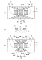
- FIG. 2A and 2B are views showing a modified example of the physical quantity sensor including the elastic wave modulation element according to the second embodiment of the present invention, where FIG. 2A is a plan view and FIG. 2B is a sectional view taken along line II-II.
- C is a bottom view.
- the present embodiment is different from the first embodiment in that the magnetostrictive material portion 15 is provided on the main surface 11b of the piezoelectric member 11 opposite to the first electrode portion 12 and the second electrode portion 13. .. Since other parts are the same as those in the first embodiment, the parts different from the first embodiment will be described below.
- the magnetostrictive material portion 21 is provided on one main surface 11b of the piezoelectric member 11 and is capable of propagating the magnetic flux of the external magnetic field.
- a magnetic flux collecting portion 21c provided between the pair of magnetic flux propagating portions 21a and 21b on the one main surface 11b and arranged near the elastic wave propagation path 14 (for example, immediately below the propagation path 14).
- the pair of magnetic flux propagating portions 21a and 21b and the magnetic flux collecting portion 21c are arranged on the one main surface 11b of the piezoelectric member 11, and the first electrode portion 12 and the second electrode portion 13 are It is arranged on the other main surface 11 a of the piezoelectric member 11. Also in this configuration, the magnetism collecting portion 21c is arranged between the first electrode portion 12 and the second electrode portion 13 on the projection surface in the thickness direction of the piezoelectric member 11 (FIGS. 2A and 2C). )reference).
- the piezoelectric member is configured to generate a Rayleigh wave of the surface acoustic wave
- the Rayleigh wave is accompanied by displacement in a direction perpendicular to the surface of the piezoelectric member. Therefore, when the magnetostrictive material portion is provided on the same main surface as the first and second electrode portions, the Rayleigh wave propagates to the magnetostrictive material portion and the attenuation becomes large, and the SAW propagation velocity cannot be sufficiently detected. There is.
- the pair of magnetic flux propagating portions 21a and 21b and the magnetic flux collecting portion 21c are provided on the main surface 11b of the piezoelectric member 11 opposite to the first electrode portion 12 and the second electrode portion 13. Therefore, when the Rayleigh wave propagates through the propagation path 14 between the first electrode portion 12 and the second electrode portion 13 and reaches the second electrode portion 13, the other main surface 11a of the piezoelectric member 11 The propagating Rayleigh wave can be suppressed from propagating to the magnetostrictive material portion 21, particularly the magnetic flux collecting portion 21c. As shown in FIG.
- the thickness of the side surface of the magnetic flux collector 21c facing the magnetic flux propagating portion 21a (and/or the magnetic flux propagating portion 21b) is equal to that of the magnetic flux propagating portion 21a (and/or the magnetic flux propagating portion 21b). It is thinner than the thickness of the side surface facing the magnetism collecting portion 21c.
- the magnetic flux collecting portion 21c is formed separately from the pair of magnetic flux propagating portions 21a and 21b, but is formed integrally with the pair of magnetic flux propagating portions 21a and 21b. May be.
- the magnetic flux inside the magnetic flux collecting portion 21c is higher than that in the magnetic flux propagating portions 21a and 21b. Greater density. Therefore, in the magnetism collecting unit 21c, the magnetostriction effect ( ⁇ E effect) accompanying the magnetism collection can be increased in addition to the ⁇ E effect accompanying the change of the magnetization state, and further, the attenuation of the Rayleigh wave propagating through the propagation path 14 can be suppressed. It is possible to suppress the change, and it is possible to sufficiently and accurately cause a change in the propagation velocity of the Rayleigh wave.
- FIG. 3A is a diagram showing a first modification of the elastic wave modulator 10 in FIG. 1
- FIG. 3C is a diagram showing a second modification.
- FIG. 3B is a sectional view taken along the line III-III.
- the magnetic flux collecting portion 15c is formed integrally with the pair of magnetic flux propagating portions 15a and 15b, but the present invention is not limited to this, and the magnetic flux collecting portion is formed separately from the pair of magnetic flux propagating portions. May be
- the magnetism collecting portion 31c of the magnetostrictive material portion 31 may be arranged so as to be spaced apart from the pair of magnetic flux propagating portions 31a and 31b.
- the magnetic flux collecting portion 31c in a plan view of the piezoelectric member 11, has a rectangular shape, and each of the pair of magnetic flux propagating portions 31a and 31b has a flat trapezoidal shape.
- the thickness of the side surface of the magnetic flux collector 31c that faces the magnetic flux propagating portion 31a (and/or the magnetic flux propagating portion 31b) is equal to the magnetic flux propagating portion 31a (and/or the magnetic flux propagating portion 31b).
- the magnetic flux collecting portion 31c is formed separately from the pair of magnetic flux propagating portions 31a and 31b. With this configuration, the magnetic flux passing through the magnetic flux propagating portion 31a or the magnetic flux propagating portion 31b passes through the magnetic flux collecting portion 31c in a denser state, so that the magnetic flux inside the magnetic flux collecting portion 31c is larger than that in the magnetic flux propagating portions 31a and 31b. Greater density.
- the magnetic flux collecting portion 32c of the magnetostrictive material portion 32 may be provided separately from the pair of magnetic flux propagating portions 32a and 32b or may be arranged separately.
- the magnetic flux collecting portion 32c has a rectangular shape
- the magnetic flux propagating portion 32a has a triangular shape with a plurality of flat rectangular portions 32a-1, 32a-1,.
- the magnetic flux propagating portion 32b includes a plurality of portions 32b-1, 32b-1,... Having a flat rectangular shape and a portion 32b-2 having a triangular shape.
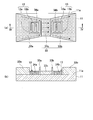
- FIG. 4A and 4B are diagrams showing a third modification of the elastic wave modulation element 10 in FIG. 1, in which FIG. 4A is a plan view and FIG. 4B is a sectional view taken along line IV-IV.
- the magnetic flux in the magnetic flux collecting portion 15c is formed along the direction perpendicular to the propagation direction of the elastic wave.
- the present invention is not limited to this. May be formed along.
- the pair of magnetic flux propagating portions 33a and 33b and the magnetic flux collecting portion 33c of the magnetostrictive material portion 33 are arranged on the one main surface 11a of the piezoelectric member 11, and the first electrode portion 12 and the second electrode portion 13 are piezoelectric. It is arranged on the one main surface 11a of the member 11 at a position corresponding to the openings 34a and 34b (non-film forming portions) provided in the pair of magnetic flux propagating portions 33a and 33b. Further, as shown in FIG.
- the thickness of the side surface of the magnetic flux collecting portion 33c that faces the magnetic flux propagating portion 33a (and/or the magnetic flux propagating portion 33b) is equal to the magnetic flux propagating portion 33a (and/or the magnetic flux propagating portion 33b). ) Is thinner than the thickness of the side surface facing the magnetism collecting portion 33c.
- the magnetic flux collecting portion 33c is formed as a separate body in contact with the pair of magnetic flux propagating portions 33a and 33b, but may be formed integrally with the pair of magnetic flux propagating portions 33a and 33b. Good.
- the magnetic flux inside the magnetic flux collecting portion 33c is higher than that of the magnetic flux propagating portions 33a and 33b. Greater density.
- a pair of magnetic flux propagating portions not having the pair of openings is provided, and the pair of magnetic flux propagating portions and magnetic flux collecting portions are arranged on one main surface 11 a of the piezoelectric member 11, and the first electrode portion 12 is provided.
- the second electrode portion 13 may be disposed on the one main surface 11a of the piezoelectric member 11 and below the pair of magnetic flux propagating portions.
- the pair of magnetic flux propagating portions and the magnetic flux collecting portion that do not have the pair of openings are arranged on the one main surface 11a of the piezoelectric member 11, and the first electrode portion 12 and the second electrode portion 13 are piezoelectric. It may be arranged on the other main surface 11b of the member 11.
- the magnetic flux in the magnetic flux collecting portion is formed along the propagation direction of the elastic wave (for example, the direction parallel to the propagation direction), and the pair of magnetic flux propagating portions 33a and 33b and the magnetic flux collecting portion 33c form one of the piezoelectric members 11.
- the first electrode portion 12 and the second electrode portion 13 may be disposed on the main surface 11a of the above, and may be disposed on one main surface of the piezoelectric member 11 and below the magnetic flux collecting portion 33c.
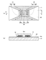
- FIG. 5A and 5B are diagrams schematically showing a configuration of an elastic wave modulator according to a third embodiment of the present invention
- FIG. 5A is a plan view
- FIG. 5B is a sectional view taken along line VV.
- the third embodiment differs from the first embodiment in that the first electrode portion 12 and the second electrode portion 13 are provided below the magnetism collecting portion.
- the explanation is omitted, and a different portion is explained below.
- the magnetism collecting portion 35c of the magnetostrictive material portion 35 is arranged so as to be separated from the pair of magnetic flux propagating portions 35a and 35b.
- the magnetism collecting portion 35c is arranged at a position including the first electrode portion 12 and the second electrode portion 13 on the projection surface projected in the thickness direction of the piezoelectric member 11.
- the first electrode portion 12 and the second electrode portion 13 are provided on the one main surface 11a of the piezoelectric member 11 and below the magnetism collecting portion 35c, the magnetostriction of the magnetism collecting portion 35c.
- the thickness of the side surface of the magnetic flux collecting portion 35c that faces the magnetic flux propagating portion 35a (and/or the magnetic flux propagating portion 35b) is equal to the magnetic flux propagating portion 35a (and/or the magnetic flux). It is thinner than the thickness of the side surface of the propagating portion 35b) facing the magnetism collecting portion 35c.
- the magnetic flux inside the magnetic flux collecting portion 35c is higher than that in the magnetic flux propagating portions 35a and 35b. Greater density. Therefore, for example, by applying the configuration of the present embodiment to a resonator-type physical quantity sensor, it is possible to improve the sensitivity as compared with the related art and to accurately detect the stress or magnetic field acting on the piezoelectric member 11.
- the pair of magnetic flux propagating portions 35 a, 35 b and the magnetic flux collecting portion 35 c are arranged on one main surface 11 a of the piezoelectric member 11, and the first electrode portion 12 and the second electrode portion 13 are arranged on the other side of the piezoelectric member 11. It may be arranged on the main surface 11b.
- the lower part of the magnetism collecting portion 35c has a comb tooth shape, and is provided between the pair of comb tooth electrodes 12a and 12b and the pair of comb teeth. It preferably penetrates between the electrodes 13a and 13b. As a result, the magnetism collecting portion 35c can be arranged at a position closer to the piezoelectric member 11, and the change in the propagation velocity of the elastic wave can be caused more efficiently.
- the elastic wave modulation element includes the piezoelectric member 11, the first electrode portion 12, and the second electrode portion from the viewpoint of preventing a short circuit between the electrodes. It is preferable to further include an insulating layer 20 formed so as to cover 13.
- the magnetic flux in the magnetic flux collecting portion 35c is formed along the direction perpendicular to the propagation direction of the elastic wave.
- the present invention is not limited to this, and the magnetic flux in the magnetic flux collecting portion 35c propagates in the elastic wave. It may be formed along the direction.
- the pair of magnetic flux propagating portions 35 a and 35 b and the magnetic flux collecting portion 35 c are arranged on the one main surface 11 a of the piezoelectric member 11, and the first electrode portion 12 and the second electrode portion 13 of the piezoelectric member 11 are arranged. It may be arranged on one main surface 11a and below the magnetic flux collector 35c, or may be arranged on the other main surface 11b of the piezoelectric member 11.
- FIG. 6A is a plan view schematically showing the configuration of a physical quantity sensor including an elastic wave modulation element according to the fourth embodiment of the present invention
- FIG. 6B is a modification of the fourth embodiment.
- FIG. In the fourth embodiment a case where the physical quantity sensor is a resonator type will be described as an example. Since the physical quantity sensor is the same as that of the third embodiment except that the physical quantity sensor is of the resonator type, only portions different from the third embodiment will be described below.
- the elastic wave modulation element 40 of the physical quantity sensor 2 is attached to the piezoelectric member 11, and a pair of reflectors 41 a arranged on both sides of the first electrode portion 12 and the second electrode portion 13. , 41b are further provided.
- the first electrode portion 12 is a comb-teeth electrode 42a (one of the pair of comb-teeth electrodes) of the pair of comb-teeth electrodes that are arranged so as to face each other so that the teeth are alternately arranged.
- the second electrode portion 13 constitutes the comb-teeth electrode 42b of the pair of comb-teeth electrodes (the other of the pair of comb-teeth electrodes).
- the comb-teeth electrode 42a and the comb-teeth electrode 42b are connected to the input/output unit 18.
- the elastic wave modulator 40 constitutes a so-called 1-port resonator.
- a pair of reflectors 41a and 41b are arranged on both sides of the pair of comb-tooth electrodes 42a and 42b, and an elastic wave excited by the pair of comb-tooth electrodes 42a and 42b is reflected by the pair of reflection waves. It is trapped between the vessels 41a and 41b.
- the pair of comb-teeth electrodes 42a and 42b are arranged on the one main surface 11a of the piezoelectric member 11 and below the magnetic flux collecting portion 15c, the propagation path 14 is caused by the magnetostriction of the magnetic flux collecting portion 15c. It is possible to more efficiently cause a change in the propagation velocity of a propagating elastic wave (or standing wave). Therefore, by applying the configuration of the present embodiment to the one-port resonator type physical quantity sensor, the sensitivity or the magnetic field acting on the piezoelectric member 11 can be detected with higher sensitivity than in the conventional case.
- the elastic wave modulator 50 of the physical quantity sensor 3 may form a so-called 2-port resonator. That is, the acoustic wave modulation element 50 may further include a pair of reflectors 51 a and 51 b attached to the piezoelectric member 11 and arranged on both sides of the first electrode portion 12 and the second electrode portion 13.
- the first electrode portion 12 is composed of a pair of comb-teeth electrodes 12a and 12b that are arranged so as to face each other so that their teeth alternate
- the second electrode portion 13 has a pair of teeth. It is composed of a pair of comb-shaped electrodes 13a and 13b which are arranged so as to be alternately arranged so as to face each other.
- the pair of comb-teeth electrodes 12 a and 12 b are connected to the input unit 17, and the pair of comb-teeth electrodes 13 a and 13 b are connected to the output unit 18. Further, the magnetostrictive material portion 15 is provided on the one main surface 11a of the piezoelectric member 11, and has a pair of magnetic flux propagating portions 36a and 36b capable of propagating the magnetic flux of the external magnetic field and a pair of magnetic flux on the one main surface 11a.
- the magnetic field collecting unit 36c is provided between the propagation units 36a and 36b, and is located near the elastic wave propagation path 14.
- the pair of comb-teeth electrodes 12a and 12b and the pair of comb-teeth electrodes 13a and 13b are both arranged on one main surface 11a of the piezoelectric member 11 and below the magnetism collecting portion 36c. Due to the magnetostriction of the magnetism collecting unit 36c, it is possible to more efficiently cause a change in the propagation velocity of the elastic wave (or standing wave) propagating in the propagation path. As described above, by applying the configuration of the elastic wave modulation element 50 to the two-port resonator type physical quantity sensor, the sensitivity is improved as compared with the conventional case by the same mechanism as in the configuration of FIG. 6A. The stress or magnetic field acting on the piezoelectric member 11 can be accurately detected.
- FIG. 7 is a plan view schematically showing the configuration of a physical quantity sensor including an elastic wave modulator according to the fifth embodiment of the present invention.
- the physical quantity sensor includes a delay line type elastic wave modulator and an antenna unit will be described as an example.
- the physical quantity sensor is the same as that of the third embodiment (FIG. 6A) except that the delay line type elastic wave modulator and the antenna section are provided, and therefore the different parts from the third embodiment will be described below.
- the elastic wave modulation element 60 of the physical quantity sensor 4 is attached to the piezoelectric member 11, and the first electrode portion 12 and the second electrode portion 13 that excite or receive the elastic wave in the piezoelectric member 11;
- the one reflector 61 attached to the member 11 and arranged on one side of the magnetic flux collector 15c is provided.
- the first electrode portion 12 and the second electrode portion are a pair of comb-teeth electrodes 43a and 43b that excite or receive elastic waves in the piezoelectric member 11.
- the comb-teeth electrode 43a of the pair of comb-teeth electrodes 43a and 43b is connected to the antenna unit 19, and the comb-teeth electrode 43b is grounded.
- the first electrode portion 12 and the second electrode portion 13 are arranged on the one main surface 11a of the piezoelectric member 11 and on the other side of the magnetism collecting portion 15c.
- the first electrode portion 12 and the second electrode portion 13 may be arranged on the one main surface 11a of the piezoelectric member 11 and below the magnetism collecting portion 13c.
- this elastic wave modulator 60 when the antenna section 19 receives a radio wave, the elastic wave excited by the pair of comb-teeth electrodes 43a and 43b reaches the reflector 61 via the propagation path 14 of the piezoelectric member 11. After that, the reflected wave generated by the reflection at the reflector 61 reaches the pair of comb-teeth electrodes 43a and 43b via the propagation path 14, and the radio wave is transmitted from the antenna unit 19.
- the magnetism collecting unit 15c is arranged on the elastic wave propagation path 14, the magnetostriction of the magnetism collecting unit 15c can more efficiently cause a change in the propagation velocity of the elastic wave propagating in the propagation path.
- the configuration of the present embodiment to a physical quantity sensor including a delay line type elastic wave modulation element and an antenna section, the stress or magnetic field acting on the piezoelectric member 11 can be wirelessly improved with higher sensitivity than before. It is possible to detect with high accuracy.
- FIG. 8 is a diagram schematically showing the configuration of a physical quantity sensor including an elastic wave modulation element according to the sixth embodiment of the present invention.
- the magnetic flux propagating portion has a trapezoidal shape in a plan view of the piezoelectric member, but the shape is not limited to this and may be a rectangular shape.
- the magnetostrictive material portion 71 of the elastic wave modulator 70 has a pair of magnetic flux propagating portions 71a and 71b and a magnetic flux collecting portion 71c, and the pair of magnetic flux propagating portions 71a and 71b collects magnetic flux. It may have a rectangular shape like the portion 71c. Since the pair of magnetic flux propagating portions 71a and 71b have a rectangular shape, it is possible to increase the degree of freedom in designing the lead wire pattern from the electrode.
- the acoustic wave modulation element 60 of FIG. 7 includes one reflector, but is not limited to this, and may include a pair of reflectors arranged on both sides of the one electrode portion and the second electrode portion. Good. At this time, the first electrode portion and the second electrode portion may be arranged on the one main surface 11a of the piezoelectric member 11 and below the magnetism collecting portion (see FIGS. 6A and 6B). ).
- the pair of reflectors 41a and 41b are attached to both sides of the magnetism collecting unit 15c, but the present invention is not limited to this.
- the magnetism collecting portion 15c may be arranged at a position including the pair of reflectors 41a and 41b on the projection surface projected in the thickness direction of the piezoelectric member 11. Further, the pair of reflectors 41a and 41b may be arranged on the one main surface 11a of the piezoelectric member 11 and below the magnetic flux collector 15c.
- the pair of reflectors 51a and 51b are attached to both sides of the magnetism collecting unit 36c, but the present invention is not limited to this.
- the magnetism collecting portion 36c may be arranged at a position including the pair of reflectors 51a and 51b on the projection surface projected in the thickness direction of the piezoelectric member 11. Further, the pair of reflectors 51a and 51b may be arranged on the one main surface 11a of the piezoelectric member 11 and below the magnetic flux collector 36c.
- the reflector 61 is attached to one side of the magnetism collecting unit 15c, but the present invention is not limited to this.
- the magnetism collecting portion 15c is arranged at a position including the one reflector 61 on the projection surface projected in the thickness direction of the piezoelectric member 11, and the one reflector 61 is provided on the one main surface 11a of the piezoelectric member 11. It may be arranged below the magnetic flux collector 15c.
- the elastic wave modulator of the present invention can be applied to various physical quantity sensors such as a magnetic field, torque, pressure and temperature.
Landscapes
- Physics & Mathematics (AREA)
- General Physics & Mathematics (AREA)
- Acoustics & Sound (AREA)
- Condensed Matter Physics & Semiconductors (AREA)
- Chemical & Material Sciences (AREA)
- Crystallography & Structural Chemistry (AREA)
- Surface Acoustic Wave Elements And Circuit Networks Thereof (AREA)
- Pressure Sensors (AREA)
Abstract
従来よりも感度を向上して被検出体の物理量を精度良く検知することができる弾性波変調素子及び物理量センサを提供する。 弾性波変調素子(10)は、圧電部材(11)と、圧電部材(11)に取り付けられ、圧電部材(11)に弾性波を励起する第1電極部(12)と、圧電部材(11)に取り付けられ、弾性波を受信する第2電極部(13)と、弾性波の存在領域またはその近傍に設けられた磁歪材料部(15)とを備える。磁歪材料部(15)は、圧電部材(11)の一方の主面(11a)上に設けられ、外部磁界の磁束を伝搬可能な一対の磁束伝搬部(15a,15b)と、一方の主面(11a)上において一対の磁束伝搬部(15a,15b)の間に設けられ、弾性波の伝搬路(14)上またはその近傍に配置された集磁部(15c)とを有し、集磁部(15c)の一対の磁束伝搬部(15a,15b)に対向する側面の厚みが、一対の磁束伝搬部(15a)の集磁部(15c)に対向する側面の厚みよりも薄い。
Description
本発明は、弾性波変調素子及び物理量センサに関し、特に、表面弾性波の伝搬特性の変化に基づいて被検出体の物理量を検出可能な弾性波変調素子に関する。
従来、表面弾性波(以下、SAW(Suface Acoustic Wave)ともいう)を用いた遅延線型や共振子型のセンサがある。遅延線型のSAWセンサの構成として、例えば、LiNbO3基板と、該基板上に設けられた一対の櫛歯電極部と、該一対の櫛歯電極部間のSAW伝搬領域に配置された非晶質TbFe2膜とを備えるSAW遅延線が提案されている(非特許文献1)。
また、遅延線型のSAWセンサとして、圧電基板と櫛歯電極を有する表面弾性波素子とアンテナ手段を備えた応答器と、上記応答器に対して駆動信号を発信すると共に、当該応答器からの応答信号を受信する問い合わせ器とからなるワイヤレスSAWセンサが提案されている。このSAWセンサは、表面弾性波の伝搬方向と一致する辺を有する略矩形状をなし、かつ上記櫛歯電極から離間している磁歪膜を備えており、矩形磁歪膜における櫛歯電極側端部からの反射波に対応するエコーと、この矩形磁歪膜における反櫛歯電極側端部からの反射波に対応するエコーとの時間差に基づいて圧電基板に働く応力を検出している(特許文献1)。
この従来技術では、圧電基板に応力が作用することより磁歪膜にも応力が作用すると、磁歪膜における磁化状態が変わり、その結果として磁歪膜と圧電基板の弾性率が変化するΔE効果が生じる。このΔE効果によって、磁歪膜と圧電基板を伝搬する表面弾性波の速度が変化する。よって、上記エコーの時間差を、圧電基板に作用する応力に対して予め校正しておくことで、当該時間差から、圧電基板に働く応力(歪)が計測することができるとされている。
山口、外2名、「非晶質TbFe2膜を用いた可変SAW遅延線(VARIABLE SAW DELAY LINE USING AMORPHOUS TbFe2 FILM)」、第16巻、第5号、1980年9月、アイトリプルイー・トランザクションズ・オン・マグネティックス(IEEE TRANSACTIONS ON MAGNETICS)
特許第5087964号公報
しかしながら、磁歪膜のいわゆるΔE効果は、磁歪膜における磁化状態の変化に依存するため、磁化状態の変化量が小さいとΔE効果が生じ難い。よって、圧電基板に働く応力が小さいと、圧電基板に働く応力を十分に検知できず、感度が良好でない場合がある。または、磁歪膜に印加された外部磁界(磁場)が小さい場合は、外部磁界による磁化状態の変化量が小さいためΔE効果も小さくなり、センサとしての磁界感度が良好でない場合がある。
本発明の目的は、従来よりも感度を向上して被検出体の物理量を精度良く検知することができる弾性波変調素子及び物理量センサを提供することにある。
上記目的を達成するために、本発明は以下の手段を提供する。
[1]圧電部材と、
前記圧電部材に取り付けられ、前記圧電部材に弾性波を励起する第1電極部と、
前記圧電部材に取り付けられ、前記弾性波を受信する第2電極部と、
前記弾性波の存在領域またはその近傍に設けられた磁歪材料部と、
を備え、
前記磁歪材料部は、
前記圧電部材の一方の主面上に設けられ、外部磁界の磁束を伝搬可能な一対の磁束伝搬部と、
前記一方の主面上において前記一対の磁束伝搬部の間に設けられ、前記弾性波の伝搬路上またはその近傍に配置された集磁部と、を有し、
前記集磁部の前記磁束伝搬部に対向する側面の厚みが、前記磁束伝搬部の前記集磁部に対向する側面の厚みよりも薄い、
ことを特徴とする弾性波変調素子。
[2]前記一対の磁束伝搬部の各々は、前記集磁部とは反対側の一端部から前記集磁部側の他端部に向かう方向に沿って断面積が小さくなる形状を有する、上記[1]記載の弾性波変調素子。
[3]前記集磁部は、前記圧電部材の厚み方向の投影面において、前記第1電極部と第2電極部との間に配置される、上記[1]または[2]に記載の弾性波変調素子。
[4]前記集磁部における磁束が、前記弾性波の伝搬方向に垂直な方向に沿って形成され、
前記一対の磁束伝搬部及び前記集磁部は、前記圧電部材の一方の主面上に配置され、
前記第1電極部及び前記第2電極部は、前記圧電部材の前記一方の主面上に配置されるか、または前記圧電部材の他方の主面上に配置される、上記[3]に記載の弾性波変調素子。
[5]前記集磁部における磁束が、前記弾性波の伝搬方向に沿って形成され、
前記一対の磁束伝搬部及び前記集磁部は、前記圧電部材の一方の主面上に配置され、
前記第1電極部及び前記第2電極部は、前記一方の主面上であって前記一対の磁束伝搬部に設けられた一対の開口部に対応する位置に配置されるか、前記一方の主面上であって前記一対の磁束伝搬部の下に配置されるか、または、前記圧電部材の他方の主面上に配置される、上記[3]に記載の弾性波変調素子。
[6]前記集磁部は、前記圧電部材の厚み方向に投影した投影面において、前記第1電極部及び前記第2電極部を包含する位置に配置される、上記[1]または[2]に記載の弾性波変調素子。
[7]前記集磁部における磁束が、前記弾性波の伝搬方向に垂直な方向に沿って形成され、
前記一対の磁束伝搬部及び前記集磁部は、前記圧電部材の一方の主面上に配置され、
前記第1電極部及び前記第2電極部が、前記圧電部材の前記一方の主面上であって前記集磁部の下に配置されるか、または前記圧電部材の他方の主面上に配置される、上記[6]に記載の弾性波変調素子。
[8]前記集磁部における磁束が、前記弾性波の伝搬方向に沿って形成され、
前記一対の磁束伝搬部及び前記集磁部は、前記圧電部材の一方の主面上に配置され、
前記第1電極部及び前記第2電極部が、前記圧電部材の前記一方の主面上であって前記集磁部の下に配置されるか、または、前記圧電部材の他方の主面上に配置される、上記[6]に記載の弾性波変調素子。
[9]前記第1電極部が、互いの歯が交互に並ぶように対向して配置された一対の櫛歯電極で構成され、
前記第2電極部が、互いの歯が交互に並ぶように対向して配置された他の一対の櫛歯電極で構成される、上記[1]~[8]のいずれかに記載の弾性波変調素子。
[10]前記第1電極部および前記第2電極部が、前記圧電部材に弾性波を励起または受信する一対の櫛歯電極である、上記[1]~[8]のいずれかに記載の弾性波変調素子。
[11]前記圧電部材に取り付けられ、前記集磁部の一方側に配置された一の反射器を更に備え、
前記第1電極部及び前記第2電極部が、前記圧電部材の一方の主面上であって前記集磁部の他方側に配置されるか、または前記圧電部材の一方の主面上であって前記集磁部の下に配置される、上記[1]~[10]のいずれかに記載の弾性波変調素子。
[12]前記集磁部は、前記圧電部材の厚み方向に投影した投影面において、前記一の反射器を包含する位置に配置され、前記一の反射器が、前記圧電部材の前記一方の主面上であって前記集磁部の下に配置される、上記[11]に記載の弾性波変調素子。
[13]前記圧電部材に取り付けられ、前記第1電極部及び前記第2電極部の両側に配置された一対の反射器を更に備える、上記[1]~[10]のいずれか1項に記載の弾性波変調素子。
[14]前記集磁部は、前記圧電部材の厚み方向に投影した投影面において、前記一対の反射器を包含する位置に配置され、前記一対の反射器が、前記圧電部材の前記一方の主面上であって前記集磁部の下に配置される、上記[13]に記載の弾性波変調素子。
[15]前記集磁部の前記磁束伝搬部に対向する側の端部の断面積が、前記の磁束伝搬部の前記集磁部に対向する側の端部の断面積よりも大きい、上記[1]~[14]のいずれか1項に記載の弾性波変調素子。
[16]上記[1]~[15]のいずれかに記載の弾性波変調素子と、前記弾性波変調素子の変調を検出する回路部と、を備える物理量センサ。
[1]圧電部材と、
前記圧電部材に取り付けられ、前記圧電部材に弾性波を励起する第1電極部と、
前記圧電部材に取り付けられ、前記弾性波を受信する第2電極部と、
前記弾性波の存在領域またはその近傍に設けられた磁歪材料部と、
を備え、
前記磁歪材料部は、
前記圧電部材の一方の主面上に設けられ、外部磁界の磁束を伝搬可能な一対の磁束伝搬部と、
前記一方の主面上において前記一対の磁束伝搬部の間に設けられ、前記弾性波の伝搬路上またはその近傍に配置された集磁部と、を有し、
前記集磁部の前記磁束伝搬部に対向する側面の厚みが、前記磁束伝搬部の前記集磁部に対向する側面の厚みよりも薄い、
ことを特徴とする弾性波変調素子。
[2]前記一対の磁束伝搬部の各々は、前記集磁部とは反対側の一端部から前記集磁部側の他端部に向かう方向に沿って断面積が小さくなる形状を有する、上記[1]記載の弾性波変調素子。
[3]前記集磁部は、前記圧電部材の厚み方向の投影面において、前記第1電極部と第2電極部との間に配置される、上記[1]または[2]に記載の弾性波変調素子。
[4]前記集磁部における磁束が、前記弾性波の伝搬方向に垂直な方向に沿って形成され、
前記一対の磁束伝搬部及び前記集磁部は、前記圧電部材の一方の主面上に配置され、
前記第1電極部及び前記第2電極部は、前記圧電部材の前記一方の主面上に配置されるか、または前記圧電部材の他方の主面上に配置される、上記[3]に記載の弾性波変調素子。
[5]前記集磁部における磁束が、前記弾性波の伝搬方向に沿って形成され、
前記一対の磁束伝搬部及び前記集磁部は、前記圧電部材の一方の主面上に配置され、
前記第1電極部及び前記第2電極部は、前記一方の主面上であって前記一対の磁束伝搬部に設けられた一対の開口部に対応する位置に配置されるか、前記一方の主面上であって前記一対の磁束伝搬部の下に配置されるか、または、前記圧電部材の他方の主面上に配置される、上記[3]に記載の弾性波変調素子。
[6]前記集磁部は、前記圧電部材の厚み方向に投影した投影面において、前記第1電極部及び前記第2電極部を包含する位置に配置される、上記[1]または[2]に記載の弾性波変調素子。
[7]前記集磁部における磁束が、前記弾性波の伝搬方向に垂直な方向に沿って形成され、
前記一対の磁束伝搬部及び前記集磁部は、前記圧電部材の一方の主面上に配置され、
前記第1電極部及び前記第2電極部が、前記圧電部材の前記一方の主面上であって前記集磁部の下に配置されるか、または前記圧電部材の他方の主面上に配置される、上記[6]に記載の弾性波変調素子。
[8]前記集磁部における磁束が、前記弾性波の伝搬方向に沿って形成され、
前記一対の磁束伝搬部及び前記集磁部は、前記圧電部材の一方の主面上に配置され、
前記第1電極部及び前記第2電極部が、前記圧電部材の前記一方の主面上であって前記集磁部の下に配置されるか、または、前記圧電部材の他方の主面上に配置される、上記[6]に記載の弾性波変調素子。
[9]前記第1電極部が、互いの歯が交互に並ぶように対向して配置された一対の櫛歯電極で構成され、
前記第2電極部が、互いの歯が交互に並ぶように対向して配置された他の一対の櫛歯電極で構成される、上記[1]~[8]のいずれかに記載の弾性波変調素子。
[10]前記第1電極部および前記第2電極部が、前記圧電部材に弾性波を励起または受信する一対の櫛歯電極である、上記[1]~[8]のいずれかに記載の弾性波変調素子。
[11]前記圧電部材に取り付けられ、前記集磁部の一方側に配置された一の反射器を更に備え、
前記第1電極部及び前記第2電極部が、前記圧電部材の一方の主面上であって前記集磁部の他方側に配置されるか、または前記圧電部材の一方の主面上であって前記集磁部の下に配置される、上記[1]~[10]のいずれかに記載の弾性波変調素子。
[12]前記集磁部は、前記圧電部材の厚み方向に投影した投影面において、前記一の反射器を包含する位置に配置され、前記一の反射器が、前記圧電部材の前記一方の主面上であって前記集磁部の下に配置される、上記[11]に記載の弾性波変調素子。
[13]前記圧電部材に取り付けられ、前記第1電極部及び前記第2電極部の両側に配置された一対の反射器を更に備える、上記[1]~[10]のいずれか1項に記載の弾性波変調素子。
[14]前記集磁部は、前記圧電部材の厚み方向に投影した投影面において、前記一対の反射器を包含する位置に配置され、前記一対の反射器が、前記圧電部材の前記一方の主面上であって前記集磁部の下に配置される、上記[13]に記載の弾性波変調素子。
[15]前記集磁部の前記磁束伝搬部に対向する側の端部の断面積が、前記の磁束伝搬部の前記集磁部に対向する側の端部の断面積よりも大きい、上記[1]~[14]のいずれか1項に記載の弾性波変調素子。
[16]上記[1]~[15]のいずれかに記載の弾性波変調素子と、前記弾性波変調素子の変調を検出する回路部と、を備える物理量センサ。
本発明によれば、従来よりも感度を向上して被検出体の物理量を精度良く検知することができる。
以下、本発明の実施形態について、図面を参照して詳細に説明する。
[弾性波変調素子及び物理量センサの構成]
図1は、本発明の第1実施形態に係る弾性波変調素子を備える物理量センサの構成を概略的に示す図であり、(a)は平面図、(b)は線I-Iに沿う断面図、(c)は底面図である。本実施形態では、物理量センサが遅延線型である場合を例に挙げて説明する。なお、以下の説明で用いる図面は、特徴をわかりやすくするために、便宜上特徴となる部分を拡大して示している場合があり、各構成要素の寸法比率等は図示するものに限らないものとする。
[弾性波変調素子及び物理量センサの構成]
図1は、本発明の第1実施形態に係る弾性波変調素子を備える物理量センサの構成を概略的に示す図であり、(a)は平面図、(b)は線I-Iに沿う断面図、(c)は底面図である。本実施形態では、物理量センサが遅延線型である場合を例に挙げて説明する。なお、以下の説明で用いる図面は、特徴をわかりやすくするために、便宜上特徴となる部分を拡大して示している場合があり、各構成要素の寸法比率等は図示するものに限らないものとする。
図1(a)~図1(c)に示すように、弾性波変調素子10は、圧電部材11と、圧電部材11に取り付けられ、圧電部材11に弾性波を励起する第1電極部12と、圧電部材11に取り付けられ、弾性波を受信する第2電極部13と、弾性波の存在領域またはその近傍に設けられた磁歪材料部15とを備える。弾性波変調素子10は、該弾性波変調素子10からの信号に基づいて弾性波の変調を検出する不図示の検出回路部に接続されており、弾性波変調素子10及び上記検出回路部が物理量センサ1を構成する。すなわち、物理量センサ1は、弾性波変調素子10及び上記検出回路部を備えており、弾性波の伝搬特性の変化に基づいて被検出体の物理量を検出する。また、物理量センサ1は、圧電部材11上の磁歪材料部15に磁界を印加する磁界印加部16を備えており、磁界印加部16が磁歪材料部15内に磁界を印加することで、磁歪材料部15内に磁界(磁場)が形成される。物理量センサ1は、例えば、圧力センサや、磁気センサなどである。
圧電部材11は、SiO2、LiNbO3、LiTaO3、BaTiO3、PbTiO3、Pb(Zr・Ti)O3(チタン酸ジルコン酸鉛)、La3Ga5SiO14、Li2B4O7、AlN(窒化アルミニウム)、ZnOおよびダイヤモンドからなる群から選択される少なくとも1つの材料で構成される。圧電部材11が上記群から選択される少なくとも1つの材料で構成されることにより、圧電部材11において弾性波を効率的に発生させることができる。圧電部材11は、例えば、圧電基板や圧電膜で構成されている。
第1電極部12は、例えば互いの歯が交互に並ぶように対向して配置された一対の櫛歯電極12a,12bで構成されている(図1(a))。この第1電極部12は、入力部17からの入力信号に基づいて弾性波、特に表面弾性波(SAW)を発生させる入力電極に相当する。第1電極部12を構成する一対の櫛歯電極12a,12bの歯のピッチは、任意に設定可能であるが、例えばλ/4(λはSAWの波長)で一定である。
また、第2電極部13は、例えば互いの歯が交互に並ぶように対向して配置された一対の櫛歯電極13a,13b(他の一対の櫛歯電極)で構成されている(図1(a))。この第2電極部13は、弾性波、特にSAWを受信して、該弾性波に対応する出力信号を出力部18を介して上記検出回路部に出力する出力電極に相当する。第2電極部13を構成する一対の櫛歯電極13a,13bの歯のピッチも、任意に設定可能であるが、例えば一対の櫛歯電極12a,12bの歯のピッチと同じである。
第1電極部12及び第2電極部13は、電極材料として適していればその材料に特に制限はないが、例えばAl(アルミニウム)、Au(金)、Cu(銅)、Ti(チタン)、Cr(クロム)、あるいはこれらの合金などの材料で構成される。
磁歪材料部15は、圧電部材11の一方の主面11a上に設けられ、外部磁界の磁束を伝搬可能な一対の磁束伝搬部15a,15bと、一方の主面11a上において一対の磁束伝搬部15a,15bの間に設けられ、弾性波の伝搬路14上に配置された集磁部15cとを有する。そして、図1(b)に示すように、集磁部15cの磁束伝搬部15a(および/または磁束伝搬部15b)に対向する側面の厚みが、磁束伝搬部15a(および/または磁束伝搬部15b)の集磁部15cに対向する側面の厚みよりも薄い。尚、本実施形態では、集磁部15cは、一対の磁束伝搬部15a,15bと当接した状態で別体で形成されているが、一対の磁束伝搬部15a,15bと一体で形成されていてもよい。上記構成により磁束伝搬部15aまたは磁束伝搬部15bを通過した磁束は、集磁部15cをより密な状態で通過するため、磁束伝搬部15a,15bと比較して集磁部15c内の磁束密度がより大きくなる。また集磁部15cは、第1電極部12と第2電極部13のうちの少なくとも一方の厚みよりも薄くして、より磁束密度を高める構成にしてもよい。
一対の磁束伝搬部15a,15bの各々は、集磁部15cとは反対側の一端部から集磁部15c側の他端部に向かう方向に沿って断面積が小さくなる形状を有しているのが好ましい。本実施形態では、物理量センサ1の平面視において、一対の磁束伝搬部15a,15bが扁平の台形状を有し、集磁部15cが矩形状を有している(図1(a)。
このように、磁歪材料部15がくびれ形状を有し、幅広な一対の磁束伝搬部15a,15bの間に幅狭な集磁部15cが配置されることで、磁歪材料部15に磁界が印加されたときに集磁部15cで確実に集磁することができる。
このように、磁歪材料部15がくびれ形状を有し、幅広な一対の磁束伝搬部15a,15bの間に幅狭な集磁部15cが配置されることで、磁歪材料部15に磁界が印加されたときに集磁部15cで確実に集磁することができる。
また、集磁部15cの磁束伝搬部15a,15bに対向する側の端部の断面積が、磁束伝搬部15a,15bの集磁部15cに対向する側の端部の断面積よりも小さいことが好ましい。集磁部15cの磁束伝搬部15a,15bに対向する側面の厚みが、磁束伝搬部15a,15bの集磁部15cに対向する側面の厚みよりも薄く、かつ、集磁部15cの上記断面積が、磁束伝搬部15a,15bの上記断面積よりも小さいことで、集磁部15c内の磁束密度を更に大きくすることができる。
但し、集磁部15cの磁束伝搬部15a,15bに対向する側の端部の断面積が、磁束伝搬部15a,15bの集磁部15cに対向する側の端部の断面積よりも大きくてもよい。これにより、たとえ集磁部15cの上記断面積が、磁束伝搬部15a,15bの上記断面積よりも大きくても、集磁部15cの厚みが、磁束伝搬部15a,15bの厚みよりも薄いことにより、集磁部15c内の磁束密度を大きくすることが可能となる。
集磁部15cは、例えば圧電部材11の厚み方向の投影面において、第1電極部12と第2電極部13との間に配置される(図1(a),(c)参照)。本実施形態では、集磁部15cにおける磁束が、弾性波の伝搬方向に垂直な方向に沿って形成される。この場合において、一対の磁束伝搬部15a,15b及び集磁部15cは、圧電部材11の一方の主面11a上に配置され、第1電極部12及び第2電極部13も、圧電部材11の一方の主面11a上に配置されている。本構成によれば、磁歪材料部15が、弾性波が伝搬する圧電部材11の一方の主面11aに当接して配置されるので、伝搬路14である一方の主面11aあるいはその近傍で、磁歪による弾性波の伝搬速度の変化をより増大させることができる。
磁歪材料部15は、Co、Ni、Fe、CoNi、NiFe、CoFe、FeAl、CoPt、NiCoCr、FeB、CoFeB、CoFeSiB、FeBSiP、FeBSiC、Ni2MnGa、FeCoNiBSi、TbFeCo、Coフェライト、Niフェライト、Cuフェライト、Liフェライト、Mnフェライト、NiCoフェライト、NiCuCoフェライト、Fe3О4、TbFe2、DyFe2、ErFe2、TmFe2、SmFe2、GaFe、Tb(0.27~0.3原子組成比率)、Dy(0.7~0.73原子組成比率)、Fe(1.9~2.0原子組成比率)からなる群から選択される少なくとも1つの材料で構成される。磁歪材料部15が上記群から選択される少なくとも1つの材料で構成されることにより、磁歪材料部15において磁歪を効率的に発生させることができる。
磁歪材料部15は、例えば磁歪膜で形成されており、その場合、一対の磁束伝搬部15a,15b及び集磁部15cも磁歪膜で形成される。磁歪材料部15の厚さは10nm~10μmである。磁歪材料部15の形成方法には制限はないが、例えばマグネトロンスパッタリングなどのスパッタリングによって成膜することができる。
磁界印加部16は、磁歪材料部15に磁歪を生じさせるための磁界を磁歪材料部15に印加する。磁歪材料部15に印加される磁界(磁場)は、磁歪効果が得られる静磁場であるのが好ましいが、変動磁場であってもよい。磁歪材料部15に印加される磁界(磁場)が静磁場である場合、磁界印加部16は、例えば永久磁石で構成される。磁界印加部16により、磁化状態を最適な動作原点とするためのバイアス磁界を与えることができる。また、磁歪材料部15の磁界印加部16とは反対側に、他の磁界印加部が設けられるのが好ましい。
[弾性波変調素子及び物理量センサの動作]
上記のように構成される弾性波変調素子10では、先ず、入力信号が第1電極部12に入力されて一対の櫛歯電極12a,12b間に電位差が生じると、一対の櫛歯電極12a,12bを介して圧電部材11に電位差が生じる。これにより、圧電部材11の表面のうち、第1電極部12が形成された部分で圧電効果によるSAWが発生する。
上記のように構成される弾性波変調素子10では、先ず、入力信号が第1電極部12に入力されて一対の櫛歯電極12a,12b間に電位差が生じると、一対の櫛歯電極12a,12bを介して圧電部材11に電位差が生じる。これにより、圧電部材11の表面のうち、第1電極部12が形成された部分で圧電効果によるSAWが発生する。
次に、圧電部材11が、例えば表面弾性波のうちのSH波(以下、SH-SAWともいう)を生じさせる構成である場合、SH-SAWは圧電部材11の主面11a或いはその近傍のうち、第1電極部12と第2電極部13の間の伝搬路14を伝搬して、第2電極部13に到達する。このとき、圧電部材11に応力が生じて、磁歪材料部15にも応力が作用すると、磁歪材料部15の磁化状態が変わり、その結果として磁歪材料部15、特に集磁部15cの弾性率が変わり(ΔE効果)、これにより、伝搬路14を伝搬するSH-SAWの伝搬速度が変わる。あるいは、磁歪材料部15に外部磁界が印加されると、ΔE効果により伝搬路14を伝搬するSH-SAWの伝搬速度が変わる。
ここで、上述のように、磁歪材料部のΔE効果は、磁歪材料部における磁化状態の変化に依存するため、磁化状態の変化量が小さいとΔE効果が生じ難い。
一方、本実施形態では、伝搬路14上に配置された集磁部15cに外部磁界の磁束が集められるため、集磁部15cの磁束密度が一対の磁束伝搬部15a,15bの磁束密度よりも高くなる。よって、集磁部15cにおける磁歪が、集磁部15cを設けない場合の非集磁部における磁歪よりも大きくなる。すなわち、集磁部15cにおいて、磁化状態の変化に伴うΔE効果に加えて、集磁に伴う磁歪効果(ΔE効果)の増大により、伝搬路14を伝搬するSH-SAWの伝搬速度が大きく変化する。よって、例えば圧電部材11に小さい応力が生じた場合、磁歪材料部15に集磁部15cを設けない場合と比較して、SH-SAWの伝搬速度の変化を十分に生じさせることができる。よって、例えば物理量センサ1を高感度な圧力センサとして機能させることができる。また、磁歪材料部15に小さい外部磁界が印加された場合にも、SH-SAWの伝搬速度の変化を十分に生じさせることができる。したがって、本実施形態の物理量センサ1を高感度な磁気センサとしても機能させることができる。
一方、本実施形態では、伝搬路14上に配置された集磁部15cに外部磁界の磁束が集められるため、集磁部15cの磁束密度が一対の磁束伝搬部15a,15bの磁束密度よりも高くなる。よって、集磁部15cにおける磁歪が、集磁部15cを設けない場合の非集磁部における磁歪よりも大きくなる。すなわち、集磁部15cにおいて、磁化状態の変化に伴うΔE効果に加えて、集磁に伴う磁歪効果(ΔE効果)の増大により、伝搬路14を伝搬するSH-SAWの伝搬速度が大きく変化する。よって、例えば圧電部材11に小さい応力が生じた場合、磁歪材料部15に集磁部15cを設けない場合と比較して、SH-SAWの伝搬速度の変化を十分に生じさせることができる。よって、例えば物理量センサ1を高感度な圧力センサとして機能させることができる。また、磁歪材料部15に小さい外部磁界が印加された場合にも、SH-SAWの伝搬速度の変化を十分に生じさせることができる。したがって、本実施形態の物理量センサ1を高感度な磁気センサとしても機能させることができる。
SAWが第2電極部13に到達すると、SAWに基づく出力信号が第2電極部13から出力される。上記出力信号が検出回路部に入力されると、検出回路部により、SAWの伝搬特性の変化に基づいて、被検出体の物理量が検出される。上記被検出体としては、例えば生体、ビルや橋などの構造物の壁や支柱、コンピューター等の電子機器、テレビや冷蔵庫等の家電製品を挙げることができ、上記物理量としては、例えば磁界、トルク、圧力、温度、ガス量などを挙げることができる。
上述したように、本実施形態によれば、磁歪材料部15が、一方の主面11a上において一対の磁束伝搬部15a,15bの間に設けられ、弾性波の伝搬路14上に配置された集磁部15cを有し、集磁部15cの磁束伝搬部15a(および/または磁束伝搬部15b)に対向する側面の厚みが、磁束伝搬部15a(および/または磁束伝搬部15b)の集磁部15cに対向する側面の厚みよりも薄いので、磁歪材料部15に外部磁界を印加したときに集磁部15cでの磁歪を増大させることができる。よって、伝搬路14を伝搬するSH-SAWの伝搬速度の変化を十分かつ効率的に生じさせることができ、従来よりも感度を向上して圧電部材11に働く磁界または応力を精度良く検知することができる。
図2は、本発明の第2実施形態に係る弾性波変調素子を備える物理量センサの変形例を示す図であり、(a)は平面図、(b)は線II-IIに沿う断面図、(c)は底面図である。本実施形態では、磁歪材料部15が、圧電部材11の第1電極部12及び第2電極部13とは反対側の主面11bに設けられている点で、上記第1実施形態とは異なる。その他の部分については第1実施形態と同様であるため、以下に第1実施形態と異なる部分を説明する。
図2(a)~(c)に示すように、磁歪材料部21は、圧電部材11の一方の主面11b上に設けられ、外部磁界の磁束を伝搬可能な一対の磁束伝搬部21a,21bと、一方の主面11b上において一対の磁束伝搬部21a,21bの間に設けられ、弾性波の伝搬路14の近傍(例えば、伝搬路14の直下)に配置された集磁部21cとを有する。
本実施形態では、一対の磁束伝搬部21a,21b及び集磁部21cは、圧電部材11の一方の主面11b上に配置されており、第1電極部12及び前記第2電極部13は、圧電部材11の他方の主面11a上に配置されている。本構成においても、集磁部21cは、圧電部材11の厚み方向の投影面において、第1電極部12と第2電極部13との間に配置されている(図2(a),(c)参照)。
ここで、圧電部材が、表面弾性波のうちのレイリー波を生じさせる構成である場合、レイリー波は圧電部材の表面に対して垂直な方向の変位を伴う。よって、磁歪材料部が第1,第2電極部と同じ主面上に設けられていると、レイリー波が磁歪材料部に伝搬して減衰が大きくなり、SAWの伝搬速度を十分に検知できない場合がある。
一方、本第2実施形態では、一対の磁束伝搬部21a,21b及び集磁部21cが、圧電部材11の第1電極部12及び第2電極部13とは反対側の主面11bに設けられているので、レイリー波が、第1電極部12と第2電極部13の間の伝搬路14を伝搬して第2電極部13に到達する際に、圧電部材11の他方の主面11aを伝搬するレイリー波が、磁歪材料部21、特に集磁部21cに伝搬するのを抑制することができる。図2(b)に示すように、集磁部21cの磁束伝搬部21a(および/または磁束伝搬部21b)に対向する側面の厚みが、磁束伝搬部21a(および/または磁束伝搬部21b)の集磁部21cに対向する側面の厚みよりも薄い。尚、本実施形態では、集磁部21cは、一対の磁束伝搬部21a,21bと当接した状態で別体で形成されているが、一対の磁束伝搬部21a,21bと一体で形成されていてもよい。上記構成により、磁束伝搬部21aまたは磁束伝搬部21bを通過した磁束は、集磁部21cをより密な状態で通過するため、磁束伝搬部21a,21bに比較して集磁部21c内の磁束密度がより大きくなる。よって、集磁部21cにおいて、磁化状態の変化に伴うΔE効果に加えて、集磁に伴う磁歪効果(ΔE効果)を増大させることができ、さらに、伝搬路14を伝搬するレイリー波の減衰を抑制することが可能となり、レイリー波の伝搬速度の変化を十分かつ正確に生じさせることができる。
図3(a)は、図1における弾性波変調素子10の第1変形例を示す図であり、図3(C)は、第2変形例を示す図である。また図3(b)は線III-IIIに沿う断面図である。
上記第1実施形態では、集磁部15cは、一対の磁束伝搬部15a,15bと一体で形成されているが、これに限られず、集磁部は一対の磁束伝搬部と別体で形成されていてもよい。
上記第1実施形態では、集磁部15cは、一対の磁束伝搬部15a,15bと一体で形成されているが、これに限られず、集磁部は一対の磁束伝搬部と別体で形成されていてもよい。
例えば、図3(a)に示すように、磁歪材料部31の集磁部31cが、一対の磁束伝搬部31a,31bと隙間を有するように離間して配置されてもよい。この場合、圧電部材11の平面視において、集磁部31cは矩形形状であり、一対の磁束伝搬部31a,31bの各々は扁平の台形状である。
また、図3(b)に示すように、集磁部31cの磁束伝搬部31a(および/または磁束伝搬部31b)に対向する側面の厚みが、磁束伝搬部31a(および/または磁束伝搬部31b)の集磁部31cに対向する側面の厚みよりも薄い。本実施形態では、集磁部31cは、一対の磁束伝搬部31a,31bと分離して形成されている。本構成により、磁束伝搬部31aまたは磁束伝搬部31bを通過した磁束は、集磁部31cをより密な状態で通過するため、磁束伝搬部31a,31bに比較して集磁部31c内の磁束密度がより大きくなる。
また、図3(b)に示すように、集磁部31cの磁束伝搬部31a(および/または磁束伝搬部31b)に対向する側面の厚みが、磁束伝搬部31a(および/または磁束伝搬部31b)の集磁部31cに対向する側面の厚みよりも薄い。本実施形態では、集磁部31cは、一対の磁束伝搬部31a,31bと分離して形成されている。本構成により、磁束伝搬部31aまたは磁束伝搬部31bを通過した磁束は、集磁部31cをより密な状態で通過するため、磁束伝搬部31a,31bに比較して集磁部31c内の磁束密度がより大きくなる。
また、図3(c)に示すように、磁歪材料部32の集磁部32cが、一対の磁束伝搬部32a,32bと別体であるか或いは離間して配置されてもよい。この場合、圧電部材11の平面視において、集磁部32cは矩形状であり、磁束伝搬部32aは、扁平の矩形状を有する複数の部位32a-1,32a-1,…と、三角形状を有する部位32a-2を有し、磁束伝搬部32bは、扁平の矩形状を有する複数の部位32b-1,32b-1,…と、三角形状を有する部位32b-2を有する。
本変形例の構成によっても、磁歪材料部31,32に外部磁界を印加したときに集磁部31c,32cでの磁歪を増大させることができる。また、設計の自由度が向上し、更には圧電部材11上に磁歪材料部31,32を容易に形成することができる。
図4は、図1における弾性波変調素子10の第3変形例を示す図であり、(a)は平面図、(b)は線IV-IVに沿う断面図である。
上記第1実施形態では、集磁部15cにおける磁束が、弾性波の伝搬方向に垂直な方向に沿って形成されているが、これに限られず、集磁部における磁束が、弾性波の伝搬方向に沿って形成されてもよい。
上記第1実施形態では、集磁部15cにおける磁束が、弾性波の伝搬方向に垂直な方向に沿って形成されているが、これに限られず、集磁部における磁束が、弾性波の伝搬方向に沿って形成されてもよい。
例えば、磁歪材料部33の一対の磁束伝搬部33a,33b及び集磁部33cは、圧電部材11の一方の主面11a上に配置され、第1電極部12及び第2電極部13は、圧電部材11の一方の主面11a上であって、一対の磁束伝搬部33a,33bに設けられた開口部34a,34b(非成膜部)に対応する位置に配置される。
また、図4(b)に示すように、集磁部33cの磁束伝搬部33a(および/または磁束伝搬部33b)に対向する側面の厚みが、磁束伝搬部33a(および/または磁束伝搬部33b)の集磁部33cに対向する側面の厚みよりも薄い。本実施形態では、集磁部33cは、一対の磁束伝搬部33a,33bと当接した状態で別体で形成されているが、一対の磁束伝搬部33a,33bと一体で形成されていてもよい。上記構成により、磁束伝搬部33aまたは磁束伝搬部33bを通過した磁束は、集磁部33cをより密な状態で通過するため、磁束伝搬部33a,33bに比較して集磁部33c内の磁束密度がより大きくなる。また、上記一対の開口部を有さない一対の磁束伝搬部を設け、該一対の磁束伝搬部及び集磁部が、圧電部材11の一方の主面11a上に配置され、第1電極部12及び第2電極部13が、圧電部材11の一方の主面11a上であって当該一対の磁束伝搬部の下に配置されてもよい。本変形例の構成によっても、磁歪材料部33に外部磁界を印加したときに集磁部33cでの磁歪を増大させることができる。
また、図4(b)に示すように、集磁部33cの磁束伝搬部33a(および/または磁束伝搬部33b)に対向する側面の厚みが、磁束伝搬部33a(および/または磁束伝搬部33b)の集磁部33cに対向する側面の厚みよりも薄い。本実施形態では、集磁部33cは、一対の磁束伝搬部33a,33bと当接した状態で別体で形成されているが、一対の磁束伝搬部33a,33bと一体で形成されていてもよい。上記構成により、磁束伝搬部33aまたは磁束伝搬部33bを通過した磁束は、集磁部33cをより密な状態で通過するため、磁束伝搬部33a,33bに比較して集磁部33c内の磁束密度がより大きくなる。また、上記一対の開口部を有さない一対の磁束伝搬部を設け、該一対の磁束伝搬部及び集磁部が、圧電部材11の一方の主面11a上に配置され、第1電極部12及び第2電極部13が、圧電部材11の一方の主面11a上であって当該一対の磁束伝搬部の下に配置されてもよい。本変形例の構成によっても、磁歪材料部33に外部磁界を印加したときに集磁部33cでの磁歪を増大させることができる。
また、上記一対の開口部を有さない一対の磁束伝搬部及び集磁部が、圧電部材11の一方の主面11a上に配置され、第1電極部12及び第2電極部13が、圧電部材11の他方の主面11b上に配置されてもよい。
更に、集磁部における磁束が、弾性波の伝搬方向(例えば、伝搬方向に平行な方向)に沿って形成され、一対の磁束伝搬部33a,33b及び集磁部33cが、圧電部材11の一方の主面11a上に配置され、第1電極部12及び第2電極部13が、圧電部材11の一方の主面上であって集磁部33cの下に配置されてもよい。
図5は、本発明の第3実施形態に係る弾性波変調素子の構成を概略的に示す図であり、(a)は平面図、(b)は線V-Vに沿う断面図である。本第3実施形態では、第1電極部12及び第2電極部13が集磁部の下に設けられている点で、上記第1実施形態と異なる。第1実施形態と同様の構成については、第1実施形態と同一の符号を付してその説明を省略し、異なる部分を以下に説明する。
図5(a)に示すように、磁歪材料部35の集磁部35cが、一対の磁束伝搬部35a,35bと隙間を有するように離間して配置されている。そして、集磁部35cは、圧電部材11の厚み方向に投影した投影面において、第1電極部12及び第2電極部13を包含する位置に配置されている。
本実施形態では、第1電極部12及び第2電極部13が、圧電部材11の一方の主面11a上であって集磁部35cの下に設けられているので、集磁部35cの磁歪により、伝搬路を伝搬する弾性波の伝搬速度の変化をより効率的に生じさせることができる。
さらに、先に図示した図3(b)と同様に、集磁部35cの磁束伝搬部35a(および/または磁束伝搬部35b)に対向する側面の厚みが、磁束伝搬部35a(および/または磁束伝搬部35b)の集磁部35cに対向する側面の厚みよりも薄い。本構成により、磁束伝搬部35aまたは磁束伝搬部35bを通過した磁束は、集磁部35cをより密な状態で通過するため、磁束伝搬部35a,35bに比較して集磁部35c内の磁束密度がより大きくなる。よって、例えば本実施形態の構成を共振子型の物理量センサに適用することで、従来よりも感度を向上して圧電部材11に働く応力または磁界を精度良く検知することができる。また、一対の磁束伝搬部35a,35b及び集磁部35cが、圧電部材11の一方の主面11a上に配置され、第1電極部12及び第2電極部13が、圧電部材11の他方の主面11b上に配置されてもよい。
さらに、先に図示した図3(b)と同様に、集磁部35cの磁束伝搬部35a(および/または磁束伝搬部35b)に対向する側面の厚みが、磁束伝搬部35a(および/または磁束伝搬部35b)の集磁部35cに対向する側面の厚みよりも薄い。本構成により、磁束伝搬部35aまたは磁束伝搬部35bを通過した磁束は、集磁部35cをより密な状態で通過するため、磁束伝搬部35a,35bに比較して集磁部35c内の磁束密度がより大きくなる。よって、例えば本実施形態の構成を共振子型の物理量センサに適用することで、従来よりも感度を向上して圧電部材11に働く応力または磁界を精度良く検知することができる。また、一対の磁束伝搬部35a,35b及び集磁部35cが、圧電部材11の一方の主面11a上に配置され、第1電極部12及び第2電極部13が、圧電部材11の他方の主面11b上に配置されてもよい。
尚、図5(b)に示すように、弾性波変調素子の断面視において、集磁部35cの下部が、櫛歯形状を有し、一対の櫛歯電極12a,12b間および一対の櫛歯電極13a,13b間に入り込んでいるのが好ましい。これにより、集磁部35cを圧電部材11により近い位置に配置することができ、弾性波の伝搬速度の変化を更に効率的に生じさせることができる。また、磁歪材料部35(特に集磁部35c)が金属で構成される場合、電極間の短絡防止の観点から、弾性波変調素子は、圧電部材11、第1電極部12および第2電極部13を覆って形成された絶縁層20を更に有するのが好ましい。
また、本実施形態では、集磁部35cにおける磁束が、弾性波の伝搬方向に垂直な方向に沿って形成されているが、これに限られず、集磁部35cにおける磁束が、弾性波の伝搬方向に沿って形成されてもよい。またこのとき、一対の磁束伝搬部35a,35b及び集磁部35cが、圧電部材11の一方の主面11a上に配置され、第1電極部12及び第2電極部13が、圧電部材11の一方の主面11a上であって集磁部35cの下に配置されるか、圧電部材11の他方の主面11b上に配置されてもよい。
図6(a)は、本発明の第4実施形態に係る弾性波変調素子を備える物理量センサの構成を概略的に示す平面図であり、図6(b)は、第4実施形態の変形例を示す平面図である。本第4実施形態では、物理量センサが共振子型である場合を例に挙げて説明する。物理量センサが共振子型であること以外は第3実施形態と同様であるため、以下に第3実施形態と異なる部分を説明する。
図6(a)に示すように、物理量センサ2の弾性波変調素子40は、圧電部材11に取り付けられ、第1電極部12及び第2電極部13の両側に配置された一対の反射器41a,41bを更に備える。本実施形態では、第1電極部12が、互いの歯が交互に並ぶように対向して配置された一対の櫛歯電極のうちの櫛歯電極42a(一対の櫛歯電極のうちの一方)を構成し、第2電極部13が、上記一対の櫛歯電極のうちの櫛歯電極42b(一対の櫛歯電極のうちの他方)を構成している。櫛歯電極42aと櫛歯電極42bは入出力部18に接続されている。弾性波変調素子40は、いわゆる1ポート共振子を構成している。
この弾性波変調素子40では、一対の反射器41a,41bが一対の櫛歯電極42a,42bの両側に配置されており、一対の櫛歯電極42a,42bによって励振した弾性波が、一対の反射器41a,41b間に閉じ込められる。このとき、一対の櫛歯電極42a,42bが圧電部材11の一方の主面11a上であって集磁部15cの下に配置されているので、集磁部15cの磁歪により、伝搬路14を伝搬する弾性波(あるいは定在波)の伝搬速度の変化をより効率的に生じさせることができる。よって、本実施形態の構成を1ポート共振子型の物理量センサに適用することで、従来よりも感度を向上して圧電部材11に働く応力または磁界を精度良く検知することができる。
また、図6(b)に示すように、物理量センサ3の弾性波変調素子50は、いわゆる2ポート共振子を構成してもよい。すなわち、弾性波変調素子50は、圧電部材11に取り付けられ、第1電極部12及び第2電極部13の両側に配置された一対の反射器51a,51bを更に備えてもよい。本変形例では、第1電極部12が、互いの歯が交互に並ぶように対向して配置された一対の櫛歯電極12a,12bで構成され、第2電極部13が、互いの歯が交互に並ぶように対向して配置された一対の櫛歯電極13a,13bで構成されている。一対の櫛歯電極12a,12bは入力部17に接続され、一対の櫛歯電極13a,13bは出力部18に接続されている。また、磁歪材料部15は、圧電部材11の一方の主面11a上に設けられ、外部磁界の磁束を伝搬可能な一対の磁束伝搬部36a,36bと、一方の主面11a上において一対の磁束伝搬部36a,36bの間に設けられ、弾性波の伝搬路14の近傍に配置された集磁部36cとを有している。
本変形例では、一対の櫛歯電極12a,12b及び一対の櫛歯電極13a,13bが共に、圧電部材11の一方の主面11a上であって集磁部36cの下に配置されているので、集磁部36cの磁歪により、伝搬路を伝搬する弾性波(あるいは定常波)の伝搬速度の変化をより効率的に生じさせることができる。このように、弾性波変調素子50の構成を2ポート共振子型の物理量センサに適用することによっても、図6(a)の構成の場合と同様のメカニズムにより、従来よりも感度を向上して圧電部材11に働く応力または磁界を精度良く検知することができる。
図7は、本発明の第5実施形態に係る弾性波変調素子を備える物理量センサの構成を概略的に示す平面図である。本第5実施形態では、物理量センサが遅延線型の弾性波変調素子とアンテナ部とを備える場合を例に挙げて説明する。物理量センサが遅延線型の弾性波変調素子とアンテナ部とを備えること以外は第3実施形態(図6(a))と同様であるため、以下に第3実施形態と異なる部分を説明する。
図7に示すように、物理量センサ4の弾性波変調素子60は、圧電部材11に取り付けられ、圧電部材11に弾性波を励起または受信する第1電極部12および第2電極部13と、圧電部材11に取り付けられ、集磁部15cの一方側に配置された一の反射器61を備える。本実施形態では、第1電極部12および第2電極部が、圧電部材11に弾性波を励起または受信する一対の櫛歯電極43a,43bである。一対の櫛歯電極43a,43bのうちの櫛歯電極43aはアンテナ部19に接続され、櫛歯電極43bは接地されている。そして、第1電極部12及び第2電極部13は、圧電部材11の一方の主面11a上であって集磁部15cの他方側に配置されている。第1電極部12及び第2電極部13は、圧電部材11の一方の主面11a上であって集磁部13cの下に配置されてもよい。
この弾性波変調素子60では、アンテナ部19で電波を受信すると、一対の櫛歯電極43a,43bによって励振した弾性波が、圧電部材11の伝搬路14を介して反射器61に到達する。その後、反射器61での反射によって生じた反射波が伝搬路14を介して一対の櫛歯電極43a,43bに到達し、アンテナ部19から電波が送信される。このとき、集磁部15cが弾性波の伝搬路14上に配置されているので、集磁部15cの磁歪により、伝搬路を伝搬する弾性波の伝搬速度の変化をより効率的に生じさせることができる。よって、本実施形態の構成を、遅延線型の弾性波変調素子とアンテナ部とを備える物理量センサに適用することで、ワイヤレスで、従来よりも感度を向上して圧電部材11に働く応力または磁界を精度良く検知することが可能となる。
図8は、本発明の第6実施形態に係る弾性波変調素子を備える物理量センサの構成を概略的に示す図である。
図1から図7の弾性変調素子では、圧電部材の平面視において、磁束伝搬部は台形状であるが、これに限らず、矩形状であってもよい。例えば、図8に示すように、弾性波変調素子70の磁歪材料部71が、一対の磁束伝搬部71a,71bおよび集磁部71cを有し、一対の磁束伝搬部71a,71bが、集磁部71cと同様に矩形状であってもよい。一対の磁束伝搬部71a,71bが矩形状であることで、電極からの引出線パターンの設計自由度を大きくすることができる。
図1から図7の弾性変調素子では、圧電部材の平面視において、磁束伝搬部は台形状であるが、これに限らず、矩形状であってもよい。例えば、図8に示すように、弾性波変調素子70の磁歪材料部71が、一対の磁束伝搬部71a,71bおよび集磁部71cを有し、一対の磁束伝搬部71a,71bが、集磁部71cと同様に矩形状であってもよい。一対の磁束伝搬部71a,71bが矩形状であることで、電極からの引出線パターンの設計自由度を大きくすることができる。
以上、本発明の実施形態について詳述したが、本発明は上記実施形態に限定されるものではなく、特許請求の範囲内に記載された本発明の要旨の範囲内において、種々の変形・変更が可能である。
例えば、図7の弾性波変調素子60は、一の反射器を備えているが、これに限らず、1電極部及び第2電極部の両側に配置された一対の反射器を備えていてもよい。またこのとき、第1電極部及び第2電極部は、圧電部材11の一方の主面11a上であって集磁部の下に配置されてもよい(図6(a),(b)参照)。
また、図6(a)において、一対の反射器41a,41bは、集磁部15cの両側に取り付けられているが、これに限られない。集磁部15cが、圧電部材11の厚み方向に投影した投影面において、一対の反射器41a,41bを包含する位置に配置されてもよい。また、一対の反射器41a,41bが、圧電部材11の一方の主面11a上であって集磁部15cの下に配置されてもよい。
同様に、図6(b)において、一対の反射器51a,51bは、集磁部36cの両側に取り付けられているが、これに限られない。集磁部36cが、圧電部材11の厚み方向に投影した投影面において、一対の反射器51a,51bを包含する位置に配置されてもよい。また、一対の反射器51a,51bが、圧電部材11の一方の主面11a上であって集磁部36cの下に配置されてもよい。
同様に、図6(b)において、一対の反射器51a,51bは、集磁部36cの両側に取り付けられているが、これに限られない。集磁部36cが、圧電部材11の厚み方向に投影した投影面において、一対の反射器51a,51bを包含する位置に配置されてもよい。また、一対の反射器51a,51bが、圧電部材11の一方の主面11a上であって集磁部36cの下に配置されてもよい。
更に、図7において、反射器61は、集磁部15cの一方側に取り付けられているが、これに限られない。集磁部15cが、圧電部材11の厚み方向に投影した投影面において、一の反射器61を包含する位置に配置され、一の反射器61が、圧電部材11の一方の主面11a上であって集磁部15cの下に配置されてもよい。
本発明の弾性波変調素子は、磁界、トルク、圧力、温度等の各種物理量センサに適用することができる。
1 物理量センサ
2 物理量センサ
3 物理量センサ
4 物理量センサ
10 弾性波変調素子
11 圧電部材
11a 主面
11b 主面
12 第1電極部
12a 櫛歯電極
12b 櫛歯電極
13 第2電極部
13a 櫛歯電極
13b 櫛歯電極
14 伝搬路
15 磁歪材料部
15a 磁束伝搬部
15b 磁束伝搬部
15c 集磁部
16 磁界印加部
17 入力部
18 出力部
19 アンテナ部
20 絶縁層
21 磁歪材料部
21a 磁束伝搬部
21b 磁束伝搬部
21c 集磁部
31 磁歪材料部
31a 磁束伝搬部
31b 磁束伝搬部
31c 集磁部
32 磁歪材料部
32a 磁束伝搬部
32a-1 部位
32a-2 部位
32b 磁束伝搬部
32b-1 部位
32b-2 部位
32c 集磁部
33 磁歪材料部
33a 磁束伝搬部
33b 磁束伝搬部
33c 集磁部
34a 開口部
34b 開口部
35 磁歪材料部
35a 磁束伝搬部
35b 磁束伝搬部
35c 集磁部
36a 磁束伝搬部
36b 磁束伝搬部
36c 集磁部
40 弾性波変調素子
41a 反射器
41b 反射器
42a 櫛歯電極
42b 櫛歯電極
43a 櫛歯電極
43b 櫛歯電極
50 弾性波変調素子
51a 反射器
51b 反射器
60 弾性波変調素子
61 反射器
70 弾性波変調素子
71 磁歪材料部
71a 磁束伝搬部
71b 磁束伝搬部
71c 集磁部
2 物理量センサ
3 物理量センサ
4 物理量センサ
10 弾性波変調素子
11 圧電部材
11a 主面
11b 主面
12 第1電極部
12a 櫛歯電極
12b 櫛歯電極
13 第2電極部
13a 櫛歯電極
13b 櫛歯電極
14 伝搬路
15 磁歪材料部
15a 磁束伝搬部
15b 磁束伝搬部
15c 集磁部
16 磁界印加部
17 入力部
18 出力部
19 アンテナ部
20 絶縁層
21 磁歪材料部
21a 磁束伝搬部
21b 磁束伝搬部
21c 集磁部
31 磁歪材料部
31a 磁束伝搬部
31b 磁束伝搬部
31c 集磁部
32 磁歪材料部
32a 磁束伝搬部
32a-1 部位
32a-2 部位
32b 磁束伝搬部
32b-1 部位
32b-2 部位
32c 集磁部
33 磁歪材料部
33a 磁束伝搬部
33b 磁束伝搬部
33c 集磁部
34a 開口部
34b 開口部
35 磁歪材料部
35a 磁束伝搬部
35b 磁束伝搬部
35c 集磁部
36a 磁束伝搬部
36b 磁束伝搬部
36c 集磁部
40 弾性波変調素子
41a 反射器
41b 反射器
42a 櫛歯電極
42b 櫛歯電極
43a 櫛歯電極
43b 櫛歯電極
50 弾性波変調素子
51a 反射器
51b 反射器
60 弾性波変調素子
61 反射器
70 弾性波変調素子
71 磁歪材料部
71a 磁束伝搬部
71b 磁束伝搬部
71c 集磁部
Claims (16)
- 圧電部材と、
前記圧電部材に取り付けられ、前記圧電部材に弾性波を励起する第1電極部と、
前記圧電部材に取り付けられ、前記弾性波を受信する第2電極部と、
前記弾性波の存在領域またはその近傍に設けられた磁歪材料部と、
を備え、
前記磁歪材料部は、
前記圧電部材の一方の主面上に設けられ、外部磁界の磁束を伝搬可能な一対の磁束伝搬部と、
前記一方の主面上において前記一対の磁束伝搬部の間に設けられ、前記弾性波の伝搬路上またはその近傍に配置された集磁部とを有し、
前記集磁部の前記磁束伝搬部に対向する側面の厚みが、前記磁束伝搬部の前記集磁部に対向する側面の厚みよりも薄い、
ことを特徴とする弾性波変調素子。 - 前記一対の磁束伝搬部の各々は、前記集磁部とは反対側の一端部から前記集磁部側の他端部に向かう方向に沿って断面積が小さくなる形状を有する、請求項1記載の弾性波変調素子。
- 前記集磁部は、前記圧電部材の厚み方向の投影面において、前記第1電極部と第2電極部との間に配置される、請求項1または2に記載の弾性波変調素子。
- 前記集磁部における磁束が、前記弾性波の伝搬方向に垂直な方向に沿って形成され、
前記一対の磁束伝搬部及び前記集磁部は、前記圧電部材の一方の主面上に配置され、
前記第1電極部及び前記第2電極部は、前記圧電部材の前記一方の主面上に配置されるか、または前記圧電部材の他方の主面上に配置される、請求項3に記載の弾性波変調素子。 - 前記集磁部における磁束が、前記弾性波の伝搬方向に沿って形成され、
前記一対の磁束伝搬部及び前記集磁部は、前記圧電部材の一方の主面上に配置され、
前記第1電極部及び前記第2電極部は、前記一方の主面上であって前記一対の磁束伝搬部に設けられた一対の開口部に対応する位置に配置されるか、前記一方の主面上であって前記一対の磁束伝搬部の下に配置されるか、または、前記圧電部材の他方の主面上に配置される、請求項3に記載の弾性波変調素子。 - 前記集磁部は、前記圧電部材の厚み方向に投影した投影面において、前記第1電極部及び前記第2電極部を包含する位置に配置される、請求項1または2に記載の弾性波変調素子。
- 前記集磁部における磁束が、前記弾性波の伝搬方向に垂直な方向に沿って形成され、
前記一対の磁束伝搬部及び前記集磁部は、前記圧電部材の一方の主面上に配置され、
前記第1電極部及び前記第2電極部が、前記圧電部材の前記一方の主面上であって前記集磁部の下に配置されるか、または前記圧電部材の他方の主面上に配置される、請求項6に記載の弾性波変調素子。 - 前記集磁部における磁束が、前記弾性波の伝搬方向に沿って形成され、
前記一対の磁束伝搬部及び前記集磁部は、前記圧電部材の一方の主面上に配置され、
前記第1電極部及び前記第2電極部が、前記圧電部材の前記一方の主面上であって前記集磁部の下に配置されるか、または、前記圧電部材の他方の主面上に配置される、請求項6に記載の弾性波変調素子。 - 前記第1電極部が、互いの歯が交互に並ぶように対向して配置された一対の櫛歯電極で構成され、
前記第2電極部が、互いの歯が交互に並ぶように対向して配置された他の一対の櫛歯電極で構成される、請求項1~8のいずれか1項に記載の弾性波変調素子。 - 前記第1電極部および前記第2電極部が、前記圧電部材に弾性波を励起または受信する一対の櫛歯電極である、請求項1~8のいずれか1項に記載の弾性波変調素子。
- 前記圧電部材に取り付けられ、前記集磁部の一方側に配置された一の反射器を更に備え、
前記第1電極部及び前記第2電極部が、前記圧電部材の一方の主面上であって前記集磁部の他方側に配置されるか、または前記圧電部材の一方の主面上であって前記集磁部の下に配置される、請求項1~10のいずれか1項に記載の弾性波変調素子。 - 前記集磁部は、前記圧電部材の厚み方向に投影した投影面において、前記一の反射器を包含する位置に配置され、
前記一の反射器が、前記圧電部材の前記一方の主面上であって前記集磁部の下に配置される、請求項11に記載の弾性波変調素子。 - 前記圧電部材に取り付けられ、前記第1電極部及び前記第2電極部の両側に配置された一対の反射器を更に備える、請求項1~10のいずれか1項に記載の弾性波変調素子。
- 前記集磁部は、前記圧電部材の厚み方向に投影した投影面において、前記一対の反射器を包含する位置に配置され、
前記一対の反射器が、前記圧電部材の前記一方の主面上であって前記集磁部の下に配置される、請求項13に記載の弾性波変調素子。 - 前記集磁部の前記磁束伝搬部に対向する側の端部の断面積が、前記磁束伝搬部の前記集磁部に対向する側の端部の断面積よりも大きい、請求項1~14のいずれか1項に記載の弾性波変調素子。
- 請求項1~15のいずれか1項に記載の弾性波変調素子と、前記弾性波変調素子の変調を検出する回路部と、を備える物理量センサ。
Priority Applications (2)
| Application Number | Priority Date | Filing Date | Title |
|---|---|---|---|
| JP2020562273A JP6885520B2 (ja) | 2018-12-28 | 2018-12-28 | 弾性波変調素子及び物理量センサ |
| PCT/JP2018/048486 WO2020136876A1 (ja) | 2018-12-28 | 2018-12-28 | 弾性波変調素子及び物理量センサ |
Applications Claiming Priority (1)
| Application Number | Priority Date | Filing Date | Title |
|---|---|---|---|
| PCT/JP2018/048486 WO2020136876A1 (ja) | 2018-12-28 | 2018-12-28 | 弾性波変調素子及び物理量センサ |
Publications (1)
| Publication Number | Publication Date |
|---|---|
| WO2020136876A1 true WO2020136876A1 (ja) | 2020-07-02 |
Family
ID=71126225
Family Applications (1)
| Application Number | Title | Priority Date | Filing Date |
|---|---|---|---|
| PCT/JP2018/048486 Ceased WO2020136876A1 (ja) | 2018-12-28 | 2018-12-28 | 弾性波変調素子及び物理量センサ |
Country Status (2)
| Country | Link |
|---|---|
| JP (1) | JP6885520B2 (ja) |
| WO (1) | WO2020136876A1 (ja) |
Citations (5)
| Publication number | Priority date | Publication date | Assignee | Title |
|---|---|---|---|---|
| CN101504446A (zh) * | 2009-03-06 | 2009-08-12 | 华南理工大学 | 薄膜式结构磁流体-声表面波集成磁传感器 |
| CN101504445A (zh) * | 2009-03-06 | 2009-08-12 | 华南理工大学 | 背槽式结构磁流体-声表面波集成磁传感器 |
| CN102435959A (zh) * | 2011-10-11 | 2012-05-02 | 电子科技大学 | 一种磁声表面波磁场传感器及其制备方法 |
| US8269490B2 (en) * | 2009-04-03 | 2012-09-18 | Honeywell International Inc. | Magnetic surface acoustic wave sensor apparatus and method |
| JP5080811B2 (ja) * | 2003-12-24 | 2012-11-21 | アイメック | 磁気セルを超高速制御するための方法及び装置 |
Family Cites Families (1)
| Publication number | Priority date | Publication date | Assignee | Title |
|---|---|---|---|---|
| JP2006047229A (ja) * | 2004-08-06 | 2006-02-16 | River Eletec Kk | 表面弾性波デバイスセンサ |
-
2018
- 2018-12-28 WO PCT/JP2018/048486 patent/WO2020136876A1/ja not_active Ceased
- 2018-12-28 JP JP2020562273A patent/JP6885520B2/ja active Active
Patent Citations (5)
| Publication number | Priority date | Publication date | Assignee | Title |
|---|---|---|---|---|
| JP5080811B2 (ja) * | 2003-12-24 | 2012-11-21 | アイメック | 磁気セルを超高速制御するための方法及び装置 |
| CN101504446A (zh) * | 2009-03-06 | 2009-08-12 | 华南理工大学 | 薄膜式结构磁流体-声表面波集成磁传感器 |
| CN101504445A (zh) * | 2009-03-06 | 2009-08-12 | 华南理工大学 | 背槽式结构磁流体-声表面波集成磁传感器 |
| US8269490B2 (en) * | 2009-04-03 | 2012-09-18 | Honeywell International Inc. | Magnetic surface acoustic wave sensor apparatus and method |
| CN102435959A (zh) * | 2011-10-11 | 2012-05-02 | 电子科技大学 | 一种磁声表面波磁场传感器及其制备方法 |
Also Published As
| Publication number | Publication date |
|---|---|
| JPWO2020136876A1 (ja) | 2021-09-09 |
| JP6885520B2 (ja) | 2021-06-16 |
Similar Documents
| Publication | Publication Date | Title |
|---|---|---|
| US12531049B2 (en) | Magnetic field sensor using acoustically driven ferromagnetic resonance | |
| US8258674B2 (en) | Surface acoustic wave sensor and system | |
| US9322809B2 (en) | Elastic wave sensor | |
| Mazzamurro et al. | Giant magnetoelastic coupling in a love acoustic waveguide based on tb co 2/fe co nanostructured film on st-cut quartz | |
| JP5087964B2 (ja) | ワイヤレス表面弾性波センサ | |
| CN107422283B (zh) | 一种具有多层磁性调制结构的低噪声磁电阻传感器 | |
| JP2007517389A (ja) | 磁気セルを超高速制御するための方法及び装置 | |
| KR101711204B1 (ko) | 단일입력 다중출력 표면탄성파 디바이스 | |
| US5847486A (en) | Love-wave device including a thin film of TA or W | |
| CN111044770A (zh) | 一种基于单端谐振器的无线无源声表面波电流传感器 | |
| US8134283B2 (en) | Vibrating element and vibrator | |
| WO2011077942A1 (ja) | 磁気センサ素子及びその製造方法並びに磁気センサ装置 | |
| Yang et al. | Sensing mechanism of surface acoustic wave magnetic field sensors based on ferromagnetic films | |
| US20120074809A1 (en) | Surface acoustic wave sensor | |
| JP2020112411A (ja) | 弾性波変調素子及び物理量センサシステム | |
| JP2006047229A (ja) | 表面弾性波デバイスセンサ | |
| CN101089907B (zh) | 传感器 | |
| CN107449955B (zh) | 一种基于图形化磁致伸缩薄膜的声表面波电流传感器 | |
| JP2020118492A (ja) | 磁気センサ素子及び磁気センサ | |
| JP6885520B2 (ja) | 弾性波変調素子及び物理量センサ | |
| JP6801832B2 (ja) | 弾性波変調素子及び物理量センサ | |
| CN117741526A (zh) | 一种基于磁斯格明子的声表面波磁场传感器 | |
| Muhammad et al. | Sensing magnetic fields with surface acoustic wave (saw) sensors | |
| Mengue et al. | Increasing the sensitivity of Love wave MSAW sensors by magnetoelastic layer thickness variation | |
| Cheng et al. | Magnetic field sensor based on magnetic torque effect and surface acoustic wave with enhanced sensitivity |
Legal Events
| Date | Code | Title | Description |
|---|---|---|---|
| 121 | Ep: the epo has been informed by wipo that ep was designated in this application |
Ref document number: 18944493 Country of ref document: EP Kind code of ref document: A1 |
|
| ENP | Entry into the national phase |
Ref document number: 2020562273 Country of ref document: JP Kind code of ref document: A |
|
| NENP | Non-entry into the national phase |
Ref country code: DE |
|
| 122 | Ep: pct application non-entry in european phase |
Ref document number: 18944493 Country of ref document: EP Kind code of ref document: A1 |