WO2020136713A1 - 発光デバイスの製造方法 - Google Patents
発光デバイスの製造方法 Download PDFInfo
- Publication number
- WO2020136713A1 WO2020136713A1 PCT/JP2018/047548 JP2018047548W WO2020136713A1 WO 2020136713 A1 WO2020136713 A1 WO 2020136713A1 JP 2018047548 W JP2018047548 W JP 2018047548W WO 2020136713 A1 WO2020136713 A1 WO 2020136713A1
- Authority
- WO
- WIPO (PCT)
- Prior art keywords
- particles
- substrate
- voltage
- electrode
- layer
- Prior art date
- Legal status (The legal status is an assumption and is not a legal conclusion. Google has not performed a legal analysis and makes no representation as to the accuracy of the status listed.)
- Ceased
Links
Images








Classifications
-
- H—ELECTRICITY
- H05—ELECTRIC TECHNIQUES NOT OTHERWISE PROVIDED FOR
- H05B—ELECTRIC HEATING; ELECTRIC LIGHT SOURCES NOT OTHERWISE PROVIDED FOR; CIRCUIT ARRANGEMENTS FOR ELECTRIC LIGHT SOURCES, IN GENERAL
- H05B33/00—Electroluminescent light sources
- H05B33/10—Apparatus or processes specially adapted to the manufacture of electroluminescent light sources
-
- H—ELECTRICITY
- H05—ELECTRIC TECHNIQUES NOT OTHERWISE PROVIDED FOR
- H05B—ELECTRIC HEATING; ELECTRIC LIGHT SOURCES NOT OTHERWISE PROVIDED FOR; CIRCUIT ARRANGEMENTS FOR ELECTRIC LIGHT SOURCES, IN GENERAL
- H05B33/00—Electroluminescent light sources
- H05B33/12—Light sources with substantially two-dimensional [2D] radiating surfaces
- H05B33/14—Light sources with substantially two-dimensional [2D] radiating surfaces characterised by the chemical or physical composition or the arrangement of the electroluminescent material, or by the simultaneous addition of the electroluminescent material in or onto the light source
-
- H—ELECTRICITY
- H05—ELECTRIC TECHNIQUES NOT OTHERWISE PROVIDED FOR
- H05B—ELECTRIC HEATING; ELECTRIC LIGHT SOURCES NOT OTHERWISE PROVIDED FOR; CIRCUIT ARRANGEMENTS FOR ELECTRIC LIGHT SOURCES, IN GENERAL
- H05B33/00—Electroluminescent light sources
- H05B33/12—Light sources with substantially two-dimensional [2D] radiating surfaces
- H05B33/26—Light sources with substantially two-dimensional [2D] radiating surfaces characterised by the composition or arrangement of the conductive material used as an electrode
-
- H—ELECTRICITY
- H10—SEMICONDUCTOR DEVICES; ELECTRIC SOLID-STATE DEVICES NOT OTHERWISE PROVIDED FOR
- H10K—ORGANIC ELECTRIC SOLID-STATE DEVICES
- H10K50/00—Organic light-emitting devices
- H10K50/10—OLEDs or polymer light-emitting diodes [PLED]
- H10K50/11—OLEDs or polymer light-emitting diodes [PLED] characterised by the electroluminescent [EL] layers
- H10K50/115—OLEDs or polymer light-emitting diodes [PLED] characterised by the electroluminescent [EL] layers comprising active inorganic nanostructures, e.g. luminescent quantum dots
Definitions
- the present invention relates to a method for manufacturing a light emitting device, in which a functional layer of the light emitting device is formed by electrodeposition.
- Patent Document 1 discloses a method of forming an organic light emitting layer by an electrodeposition method in the production of an organic light emitting element.
- a method for producing a light emitting device of the present invention is a method for producing a light emitting device in which functional particles are electrodeposited on a substrate electrode formed on a substrate, the substrate and the substrate A substrate gripping step of sandwiching an electrodeposition liquid containing first particles and second particles different from the first particles as the functional particles between the counter electrodes arranged in parallel; A first film forming step of applying a first voltage between the first substrate electrode of the substrate electrodes and the counter electrode to form the first particles on the first substrate electrode; Subsequent to the first film forming step, a second voltage is applied between the second substrate electrode of the substrate electrodes and the counter electrode to form the second particles on the second substrate electrode. A second film forming step, wherein the absolute value of the first voltage is smaller than the absolute value of the second voltage.
- the tact time in manufacturing a light emitting device can be shortened.
- FIG. 6A to 6D are process cross-sectional views for explaining the method for manufacturing the light-emitting device according to the first embodiment of the present invention. It is a schematic diagram of a substrate concerning Embodiment 1 of the present invention.
- 1 is a schematic diagram of a light emitting device manufacturing apparatus according to a first embodiment of the present invention.
- FIG. 3 is a schematic view of the manufacturing apparatus of the light emitting device according to Embodiment 1 of the present invention in a state where the substrate is pressed against the electrodeposition tank.
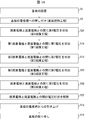
- 3 is a flowchart illustrating a method of manufacturing the light emitting device according to the first embodiment of the invention.
- FIG. 3 is a schematic view of functional particles contained in the electrodeposition liquid according to the first embodiment of the present invention.
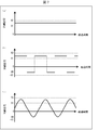
- FIG. 7 is a graph showing a relationship between applied voltage and elapsed time in an electrodeposition process using the light emitting device manufacturing apparatus according to the first embodiment and the modification of the present invention.
- FIG. 3 is a cross-sectional view of the light-emitting device manufacturing apparatus and the substrate for explaining the problems in the light-emitting device manufacturing method according to the first embodiment of the present invention. It is the schematic of the board
- FIG. 6 is a flowchart illustrating a method for manufacturing a light emitting device according to a second embodiment of the invention.
- FIG. 6 is a process cross-sectional view for explaining an electrodeposition process according to Embodiment 2 of the present invention.
- FIG. 7 is a process cross-sectional view for explaining an electrodeposition process using the display device manufacturing apparatus according to the second embodiment of the present invention in comparison with an electrodeposition process using the display device manufacturing apparatus according to the comparative embodiment.
- 6 is a flowchart for explaining a method for manufacturing a light emitting device according to Embodiment 3 of the present invention.
- FIG. 6 is a process cross-sectional view for explaining an electrodeposition process according to Embodiment 3 of the present invention.
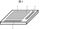
- FIG. 2 is a schematic perspective view of the substrate C according to this embodiment.
- the substrate C includes a single flat electrode U and an electrodeposition bath connection electrode D as substrate electrodes.
- the flat electrode U is formed on the substrate C so as to be exposed on one of the surfaces of the substrate C.
- the plane electrode U is formed in a rectangular shape on the substrate C.
- the electrodeposition bath connecting electrode D is formed on any two sides of the substrate C orthogonal to each other on the surface of the substrate C on which the planar electrode U is formed. Since the flat electrode U and the electrodeposition bath connecting electrode D are electrically connected to each other, a voltage can be applied to the flat electrode U by applying a voltage to the electrodeposition bath connecting electrode D. As long as the electrodeposition bath connection electrode D is formed on the surface of the substrate C on which the planar electrode U is formed, the electrodeposition bath connection electrode D is not limited to be formed along two orthogonal sides of the substrate C, but also the substrate C. The shape is not particularly limited, such as being provided only along any one of the sides.
- the flat electrode U and the electrodeposition bath connection electrode D are flush with the surface of the substrate C on which the flat electrode U and the electrodeposition bath connection electrode D are formed, and are exposed at the surfaces.
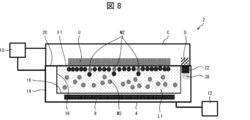
- FIG. 3 is a schematic diagram of the light emitting device manufacturing apparatus 2 according to the present embodiment.
- FIG. 3A is a perspective view of the light emitting device manufacturing apparatus 2.
- FIG. 3B is a top view of the light emitting device manufacturing apparatus 2.
- 3C is a cross-sectional view taken along the line AA in FIG. It should be noted that FIG. 3A illustrates a state where the substrate C is installed in the light emitting device manufacturing apparatus 2. However, for simplicity of illustration, the illustration of the substrate C is omitted in FIGS. 3B and 3C.
- the top view of the light-emitting device manufacturing apparatus 2 in each drawing is a top view at a position corresponding to (b) of FIG. 3 unless otherwise specified.
- the cross-sectional view of the light-emitting device manufacturing apparatus 2 in each drawing is a cross-sectional view at a position corresponding to (c) of FIG. 3 unless otherwise specified.
- the light emitting device manufacturing apparatus 2 includes an electrodeposition tank 4, a bottom electrode 8, a pressing unit 10, and an electrodeposition power source 12.
- the electrodeposition tank 4 includes an outer side surface 14 that defines the outer shape of the electrodeposition tank 4, and an inner side surface 16 and a bottom surface 18 that define the inside 4A of the electrodeposition tank 4.
- An edge portion 20 is defined between the outer side surface 14 and the inner side surface 16.
- a plurality of substrate connecting electrodes 22 are formed on the upper surface of the edge portion 20. That is, a plurality of substrate connecting electrodes 22 are formed on the outer periphery of the electrodeposition tank 4.
- the bottom electrode 8 is formed on the bottom surface 18 of the electrodeposition tank 4.
- the bottom surface electrode 8 is flush with the bottom surface 18 and is exposed from the bottom surface 18. Further, when the substrate C is installed in the light emitting device manufacturing apparatus 2, the bottom surface electrode 8 serves as a counter electrode facing the flat electrode U formed on the substrate C.
- the pressurizing unit 10 has a mechanism for moving at least one of the substrate C and the electrodeposition tank 4 to control the relative distance between the substrate C and the electrodeposition tank 4.
- the substrate C is placed in the manufacturing apparatus 2 for a light emitting device by disposing the substrate C in the pressure unit 10.
- the substrate C is disposed so that the planar electrode U of the substrate C faces the bottom electrode 8 of the electrodeposition tank 4 in parallel.
- the pressing unit 10 may be, for example, a vacuum chuck that holds the substrate C.
- the pressurizing unit 10 may control the relative distance between the substrate C and the electrodeposition tank 4 by moving the substrate C with respect to the electrodeposition tank 4.
- the pressurizing unit 10 can bring the substrate C and the electrodeposition tank 4 close to each other until the substrate C and the electrodeposition tank 4 come close to each other.
- 4A and 4B are schematic diagrams corresponding to FIGS. 3A and 3C in a state where the substrate C and the electrodeposition tank 4 are pressed against each other. Shown respectively. 4B, the cross section of the substrate C is also illustrated.
- the bottom electrode 8 faces the flat electrode U of the substrate C via the inside 4A, as shown in FIG. 4(b). That is, when the substrate C and the electrodeposition tank 4 are pressed against each other, the inside 4A is sandwiched between the substrate C and the bottom electrode 8 that is parallel to the substrate C.
- the electrode 22 for connecting the substrate of the electrodeposition bath 4 and the electrode D for connecting the electrodeposition bath of the substrate C come into contact with each other and become electrically conductive with each other.
- the electrodeposition bath 4 serves to assist the electrical continuity between the substrate connection electrode 22 and the electrodeposition bath connection electrode D.
- a spring 38 that pushes up the substrate connection electrode 22 may be provided below each substrate connection electrode 22.
- the interior 4A defined by the side surface 16 and the bottom surface 18 has a distance d1 from the upper surface of the edge portion 20 to the upper surface of the bottom electrode 8.
- This distance d1 corresponds to the depth of the interior 4A, and as shown in FIG. 4B, when the substrate C and the electrodeposition bath 4 are pressed against each other, the bottom electrode 8 and the flat electrode U are separated from each other. Substantially equal to the distance between.
- the electrodeposition power source 12 is a power source that applies at least a binary voltage to the bottom surface electrode 8 and the substrate connecting electrode 22. Further, the electrodeposition power source 12 may apply a voltage to the planar electrode U of the substrate C via the substrate connecting electrode 22 and the electrodeposition bath connecting electrode D. Therefore, the electrodeposition power source 12 may apply at least a binary voltage between the flat electrode U and the bottom electrode 8.
- the substrate connection electrode 22 is also not particularly limited.
- the electrode 22 for substrate connection is the electrodeposition bath connection electrode when the substrate C and the electrodeposition bath 4 are pressed against each other. It may be formed along one side of the upper surface of the edge portion 20 that overlaps with D.
- FIG. 5 is a flowchart for explaining an example of a manufacturing method using the light emitting device manufacturing apparatus 2 according to the present embodiment.
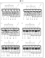
- FIG. 1 is a process cross-sectional view of a light emitting device manufacturing apparatus 2 and a substrate C in the manufacturing method shown in FIG.
- step S2 is performed, for example, by placing the substrate C on the pressing unit 10 so that the planar electrode U of the substrate C faces the bottom electrode 8.
- the inside 4A is filled with the electrodeposition liquid L1 before the substrate C installed in the pressurizing unit 10 is brought close to the electrodeposition tank 4 in step S2.
- the electrodeposition liquid L1 contains a plurality of functional particles.
- the functional particles contained in the electrodeposition liquid L1 are dispersed in the electrodeposition liquid L1 which is a solvent.
- the electrodeposition liquid L1 include water, alkyl alcohol, toluene, propylene glycol monomethyl ether acetate (PGMEA), alkane, and the like.
- the functional particles contained in the electrodeposition liquid L1 may be, for example, the material of the functional layer of the light emitting element.
- the functional layer of the light emitting element include an electron transport layer, a light emitting layer, or a hole transport layer formed between electrodes of the light emitting element.
- the functional particles when the functional particles are the material of the light emitting layer, the functional particles may be self-luminous particles.
- the functional particles in the present embodiment may include inorganic nanoparticles, and particularly may include semiconductor nanoparticles, that is, quantum dots.
- the functional particles in the present embodiment are the nanoparticle material of the light emitting layer
- the functional particles may have a single core structure made of CdSe, ZnSe, InP or the like.
- the functional particles in the present embodiment may have a core/shell structure composed of CdSe/ZnS, InP/ZnS, CdSe/CdS, ZnSe/ZnS, or the like.
- the functional particles in the present embodiment may have a multi-shell structure composed of CdSe/ZnSe/ZnS or the like.
- the functional particles in the present embodiment are the nanoparticle material of the electron transport layer, even if the functional particles include ZnO, ZrO, MgZnO, AlZnO, TiO 2 , Ta 2 O 3 , SrTiO 3 or the like. Good.
- the functional particles in the present embodiment are the nanoparticle material of the hole transport layer, the functional particles may include NiO, CuI, Cu 2 O, CoO, Cr 2 O 3 or MoO 3. Good.
- the electrodeposition liquid L1 includes, as functional particles, first particles M1 and second particles M2 which are particles different from each other as functional particles, as shown in (a) of FIG.
- first particles M1 and the second particles M2 are materials for the light emitting layer
- the first particles M1 and the second particles M2 may be self-luminous particles that emit different lights.
- the functional particles contained in the electrodeposition liquid L1 may include a ligand that forms a coordinate bond with each of the functional particles.
- the first particles M1 may have a structure in which the first ligand R1 is coordinated around, and the second particles M2 are It may have a structure in which a second ligand R2 different from the one ligand R1 is coordinated.
- the ligand in the present embodiment include mercaptoalkanoic acid, alkanethiol, alkylamine, alkane, alkene, trioctylphosphine (TOP), trioctylphosphine oxide (TOPO), and the like.
- step S4 the pressurizing unit 10 is controlled to press the substrate C against the electrodeposition tank 4 (step S4).
- step S4 As shown in FIG. 1B, the surface of the substrate C on which the planar electrode U is formed and the upper surface of the edge portion 20 are in contact with each other.
- the substrate gripping step of sandwiching the electrodeposition liquid L1 filled in the interior 4A between the substrate C and the bottom electrode 8 parallel to the substrate C is performed.
- the inside 4A is filled with the electrodeposition liquid L1
- the inside 4A is filled such that the liquid surface of the electrodeposition liquid L1 in the inside 4A is slightly higher than the upper surface of the edge portion 20 due to the surface tension. ..
- the substrate C may be thinly formed only in the portion contacting the edge portion 20 in step S4.
- the surface of the flat electrode U enters into the interior 4A more than the upper surface of the edge portion 20, so that the surface of the flat electrode U is more surely contacted. Be immersed in.
- the electrodeposition tank connection electrode D formed on the substrate C and the upper surface of the edge portion 20.
- the substrate connecting electrode 22 exposed from the abutment is brought into contact with and electrically connected.
- step S4 the electrodeposition process is performed.
- the first particles M1 and the second particles M2 have polarities by having a specific functional group. Therefore, in the electrodeposition step, the first particles M1 and the second particles M2 migrate in the electrodeposition liquid L1 by Coulomb interaction due to the electric field generated between the bottom electrode 8 and the flat electrode U. Further, the first particles M1 and the second particles M2 have the same polarity. In the present embodiment, in the electrodeposition step, the voltage applied to each electrode is controlled so that the first particles M1 and the second particles M2 migrate toward the flat electrode U.
- each of the first particles M1 and the second particles M2 has a threshold voltage between the bottom electrode 8 and the plane electrode U, which is necessary for being adsorbed to the plane electrode U and forming a film on the plane electrode U.
- Each is different.
- the threshold voltage for each functional particle differs depending on the particle size of the functional particle, the type of ligand to be coordinated, or the number of coordinations to one functional particle.
- the absolute value of the first threshold voltage V1 that is the threshold voltage for the first particles M1 is lower than the absolute value of the second threshold voltage V2 that is the threshold voltage for the second particles M2. That is, the first particles M1 are adsorbed to the flat electrode U to form a film under an electric field between the bottom electrode 8 and the flat electrode U, which are smaller than the second particles M2.
- the first voltage whose absolute value is equal to or more than the absolute value of the first threshold voltage V1 and less than the absolute value of the second threshold voltage V2 is applied to the bottom electrode 8
- the first film forming step of applying the voltage between the substrate and the flat electrode U is performed (step S6).
- step S6 as shown in (c) of FIG. 1, among the functional particles contained in the electrodeposition liquid L1, only the first particles M1 migrate to the flat electrode U and are adsorbed on the flat electrode U.
- step S6 By sufficiently applying the voltage in step S6, the first layer F1 including the first particles M1 shown in FIG. 1C is formed on the planar electrode U.
- step S6 is performed until almost all of the first particles M1 in the electrodeposition tank 4 are adsorbed on the flat electrode U for forming the first layer F1.
- step S6 a second film forming step of applying a second voltage whose absolute value is greater than or equal to the absolute value of the second threshold voltage V2 between the bottom electrode 8 and the flat electrode U (step) is performed. S8).
- the second particles M2 also migrate to the flat electrode U and are adsorbed on the flat electrode U.
- the second layer F2 including the second particles M2 shown in (d) of FIG. 1 is formed on the first layer F1.
- the second layer F2 may contain a small amount of the first particles M1 as long as the density of the first particles M1 in the second layer F2 is lower than the standard of the defect as a final light emitting device. Therefore, in the present embodiment, a slight amount of the first particles M1 may be included in the electrodeposition tank 4 in step S8.
- the present embodiment exemplifies a case where the functional material contained in the electrodeposition liquid L1 has a negative polarity. That is, a voltage of negative polarity is applied to the bottom electrode 8 and a voltage of positive polarity is applied to the plane electrode U. When the polarities of the functional material contained in the electrodeposition liquid L1 are reversed, the polarities of the voltages applied to the electrodes may be reversed.
- step S10 the voltage application between the bottom electrode 8 and the flat electrode U is released (step S10), and the electrodeposition process is completed.
- the substrate C is pulled up from the electrodeposition bath 4 (step S12).
- Step S12 is executed by controlling the pressurizing unit 10 and separating the substrate C from the electrodeposition tank 4.
- the substrate C is removed from the pressing unit 10 (step S14) to obtain the substrate C in which the first layer F1 and the second layer F2 are laminated on the flat electrode U from the lower layer.
- the light emitting device may be manufactured by forming a counter substrate or the like on the upper layer of the second layer F2.
- the tact time can be reduced even when a plurality of layers respectively containing different functional materials are formed.
- the first substrate electrode which is an electrode that applies the first voltage to the bottom electrode 8
- the second substrate electrode which is the electrode that applies the second voltage to the bottom electrode 8.
- a plurality of layers respectively containing different functional materials can be formed on the same plane electrode U by being laminated.
- the mixing of the first particles M1 and the second particles M2 of the electrodeposition liquid L1 is preferably performed in step S6, that is, immediately before the first film forming step.
- step S6 that is, immediately before the first film forming step.
- adsorption and desorption of ligands may occur between the first particles M1 and the second particles M2. This is because ligand movement occurs equilibrium between the first particles M1 and the second particles M2. Therefore, when a long time has passed since the first particles M1 and the second particles M2 were mixed, as shown in FIG. 6B, both the first particles M1 and the second particles M2 Both the first ligand R1 and the second ligand R2 may change to a coordinated state.
- the above-mentioned equilibration of the ligand is less likely to occur. For this reason, the ligand composition of the first particles M1 and the second particles M2 in the electrodeposition liquid L1 is more clearly different, so that the characteristics of the first particles M1 and the second particles M2 can be more clearly different. .. Therefore, the absolute values of the first threshold voltage V1 and the second threshold voltage V2 can be made to differ more clearly, and as a result, the yield of film formation of each functional particle is improved.
- the mixing of the first particles M1 and the second particles M2 may be performed, for example, together with the filling of the electrodeposition liquid L1 into the electrodeposition tank 4.
- Electrodeposition in this specification includes an electrochemical film forming method for forming a thin film of a material in a solution by causing a potential difference between two electrodes in the solution.
- Electrodeposition in the present specification includes, for example, methods such as electrodeposition method, electrodeposition coating method, electrophoretic deposition method, dielectrophoretic deposition method, micelle electrolysis method, electroplating method and electroforming method. Good. Even when any one of these methods is selected as the electrodeposition step described above, it is possible to manufacture a light emitting device that achieves the effects described above.
- the voltage application in step S6 is, for example, as shown in the graph of FIG. 7A, between the bottom electrode 8 and the plane electrode U, always higher than or equal to the first threshold voltage and lower than the second threshold voltage V2. It may be realized by continuing to apply the first voltage.
- step S6 is not limited to this, and the first voltage is applied between the bottom electrode 8 and the plane electrode U as shown in FIG. 7B.
- the reverse voltage VR (eighth voltage) may be alternately applied. That is, step S6 is realized by alternately performing the forward voltage applying step of applying the first voltage and the reverse voltage applying step of applying the reverse voltage VR between the bottom electrode 8 and the flat electrode U. You may.
- the reverse voltage VR has a polarity opposite to that of the first threshold voltage V1.
- the absolute value of the reverse voltage VR is smaller than the first threshold voltage V1 as shown in FIG. 7B.
- the period of the reverse voltage applying step of applying the reverse voltage VR is shorter than the period of the forward voltage applying step of applying the first voltage. May be.
- step S6 as shown in the graph of FIG. 7A, when the first voltage is continuously applied between the bottom electrode 8 and the plane electrode U, the first particles M1 are always on the plane electrode side. It will continue to migrate. Further, although the second particles M2 are not adsorbed on the flat electrode U, they migrate in the direction of the flat electrode U, so that the density of the second particles M2 also increases on the flat electrode U side in the electrodeposition tank 4. ing.
- the second particles M2 caught in the first particles M1 may be adsorbed by the flat electrode U so as to be held by the first particles M1. Therefore, in the above-mentioned case, as shown in the process sectional view of the manufacturing apparatus 2 for a light emitting device at the time of completion of step S6 shown in FIG. There is.
- step S6 as shown in the graph of FIG. 7B, the forward voltage applying step and the reverse voltage applying step are alternately performed, so that the first particles M1 and the second particles M1
- the particles M2 migrate toward the bottom electrode 8. Therefore, the first particles M1 and the second particles M2 repeat the migration to the bottom electrode 8 side and the migration to the flat electrode U side. Since the first voltage is applied in the forward voltage applying step, the first particles M1 gradually approach the flat electrode U while repeating the migration to the bottom electrode 8 side and the migration to the flat electrode U side. Finally, it is adsorbed on the flat electrode U.
- the second electrode M2 Since the first particles and the second particles repeat the migration to the bottom electrode 8 side and the migration to the flat electrode U side, the second electrode M2 is held by the first particle M1 so that the flat electrode is held. The possibility of being adsorbed by U is reduced. Therefore, it is possible to reduce the occurrence of a film formation defect in which the second particles M2 are contained in the first layer F1. Since the absolute value of the reverse voltage VR is smaller than the absolute value of the first voltage V1, it is possible to reduce the adsorption of the first particles M1 to the bottom surface electrode 8.
- the method of alternately performing the forward voltage applying step and the reverse voltage applying step is not limited to the method of alternately applying the first voltage and the reverse voltage VR as shown in the graph of FIG. 7B. Absent.
- the voltage may be applied so that the voltage between the bottom electrode 8 and the plane electrode U draws a sine wave with the elapsed time as the horizontal axis.
- the maximum value of the sine wave may be the first voltage and the minimum value may be the reverse voltage VR.
- the above-mentioned effects can be obtained similarly.
- the voltage between the bottom surface electrode 8 and the plane electrode U may draw a pseudo sine wave or a triangular wave with the elapsed time as the horizontal axis.
- FIG. 9 is a schematic perspective view of the substrate C according to this embodiment.
- the substrate C shown in FIG. 9 differs from the substrate C shown in FIG. 1 only in that it includes a plurality of pixel electrodes E instead of the planar electrodes U and a plurality of electrodeposition bath connection electrodes D.
- the pixel electrode E is patterned on the substrate C so as to be exposed on either surface of the substrate C.
- the pixel electrodes E are formed in a matrix on the substrate C.
- a plurality of electrodeposition bath connection electrodes D are formed on the surface of the substrate C on which the pixel electrodes E are formed, along any two sides of the substrate C orthogonal to each other.
- a voltage can be applied to each pixel electrode E by applying a voltage to each electrodeposition bath connecting electrode D.
- a plurality of transistors (not shown) connected to each pixel electrode E may be formed on the substrate C, and each transistor is driven by applying a voltage to each electrodeposition tank connection electrode D.
- a voltage may be applied to each pixel electrode E.
- the pixel electrode E and the electrodeposition bath connection electrode D are flush with the surface of the substrate C on which the pixel electrode E and the electrodeposition bath connection electrode D are formed, and are exposed on the surface.
- electrodeposition on the substrate C is performed using the light emitting device manufacturing apparatus 2.
- the light emitting device manufacturing apparatus 2 in the present embodiment may have the same configuration as the light emitting device manufacturing apparatus 2 in the previous embodiment.
- 10A and 10 are schematic diagrams corresponding to FIGS. 3A and 3C in a state where the substrate C and the electrodeposition tank 4 are pressed against each other in the present embodiment. (B) of each.
- the electrodeposition power source 12 can individually apply a voltage to each of the pixel electrodes E on the substrate C via the substrate connection electrode 22 and the electrodeposition bath connection electrode D. Therefore, the electrodeposition power source 12 applies at least a binary voltage between each pixel electrode E and the bottom electrode 8.
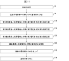
- FIG. 11 is a flowchart for explaining an example of a manufacturing method using the light emitting device manufacturing apparatus 2 according to the present embodiment.
- FIG. 12 is a process cross-sectional view of the light emitting device manufacturing apparatus 2 and the substrate C in the manufacturing method shown in FIG. 12 is an enlarged side view of the vicinity of the electrodeposition tank 4 in the electrodeposition process of this embodiment.
- the substrate C includes, as pixel electrodes E, a plurality of first pixel electrodes E1, second pixel electrodes E2, and third pixel electrodes E3, as shown in the drawings of FIG. There is.
- a method of forming layers made of functional particles different from each other on each of the first pixel electrode E1, the second pixel electrode E2, and the third pixel electrode E3 will be described.
- step S2 the substrate C is installed in the light emitting device manufacturing apparatus 2 (step S2).
- step S2 is executed as in the previous embodiment.
- the inside 4A is filled with the electrodeposition liquid L2 different from the electrodeposition liquid L1.
- the electrodeposition liquid L2 may contain the same solvent as the solvent of the electrodeposition liquid L1.
- the electrodeposition liquid L2 contains, as functional particles, third particles M3 in addition to the first particles M1 and the second particles M2 described in the previous embodiment. Similar to the first particles M1 and the second particles M2, the third particles M3 may be the material of the functional layer of the light emitting element, or may be semiconductor nanoparticles, that is, quantum dots.
- the third particles M3 have the same polarity as the first particles M1 and the second particles M2.
- the bottom electrode 8 and the pixel electrode E which are necessary for the first particles M1 and the second particles M2 to be adsorbed on any of the pixel electrodes E and to be deposited on the pixel electrodes E
- the first threshold voltage V1 and the second threshold voltage V2 are respectively provided as the threshold voltages between the two.
- the absolute value of the third threshold voltage V3, which is the threshold voltage required for the third particles M3 to be adsorbed on any of the pixel electrodes E and to be formed on the pixel electrodes E is the second threshold voltage. Greater than the absolute value of V2.
- step S4 the pressurizing unit 10 is controlled to press the substrate C against the electrodeposition tank 4, and the substrate holding step is performed (step S4).
- the pixel electrode E on the substrate C is immersed in the electrodeposition liquid L2.
- an electrodeposition step is performed.
- the first voltage whose absolute value is equal to or more than the absolute value of the first threshold voltage V1 and less than the absolute value of the second threshold voltage V2 is applied to the bottom electrode 8
- a first pixel electrode E1 is applied between the first film forming step (step S16).
- step S16 as shown in (a) of FIG. 12, among the functional particles contained in the electrodeposition liquid L2, only the first particles M1 migrate to the first pixel electrode E1, and the first particles M1 are deposited on the first pixel electrode E1. Adsorbed.
- step S16 By sufficiently applying the voltage in step S16, the first layer F1 including the first particles M1 shown in FIG. 12B is formed on the first pixel electrode E1. Note that step S16 is performed until almost all of the first particles M1 in the electrodeposition tank 4 are adsorbed on the first pixel electrode E1 for forming the first layer F1.
- FIGS. 13A and 13B are process cross-sectional views for explaining the electrodeposition process using the light emitting device manufacturing apparatus 2 according to the present embodiment.
- 13C and 13D are process cross-sectional views for explaining an electrodeposition process using the light emitting device manufacturing apparatus according to the comparative embodiment.
- the light emitting device manufacturing apparatus is related to the present embodiment, except that, instead of the electrodeposition tank 4, it is provided with an electrodeposition tank 4C having a distance d2 larger than the distance d1 as a depth.
- the light emitting device manufacturing apparatus 2 has the same configuration.
- the voltage applied to the first pixel electrode E1B of the first pixel electrodes E1 is lower than the desired voltage with respect to the first pixel electrode E1A.
- the electric field generated between the bottom electrode 8 and the first pixel electrode E1B is weaker than the electric field generated between the bottom electrode 8 and the first pixel electrode E1A.
- the first layer F1 formed on each of the first pixel electrode E1A and the first pixel electrode E1B is referred to as a first layer F1A and a first layer F1B, respectively.
- the film formation rate of the first layer F1B becomes slower than the film formation rate of the first layer F1A.
- the first particles M1 existing in the vicinity of a specific pixel electrode E decrease due to the film formation of the first layer F1, and the film formation rate of the first particles M1 on the pixel electrode E rapidly decreases. ..
- the film forming rate of the first layer F1A is relatively high, the first particles M1 near the first pixel electrode E1A are consumed relatively quickly.
- the electrodeposition tank 4 having the depth of the relatively short distance d1 as in the present embodiment the total amount of the first particles M1 in the electrodeposition tank 4 is relatively small. Therefore, in the film forming step, the first particles M1 in the vicinity of the first pixel electrode E1A rapidly decrease, and therefore, after the first layer F1A is continuously formed for a while, the film forming rate of the first layer F1A is Falls rapidly.
- the film formation rate of the first layer F1B is relatively slow, the first particles M1 still remain in the vicinity of the first pixel electrode E1B even when the film formation rate of the first layer F1A rapidly decreases. ing. For this reason, as time further elapses, the film formation of the first layer F1B continues even after the film formation of the first layer F1A is substantially stopped. The film formation of the first layer F1B continues until the amount of the first particles M1 near the first pixel electrode E1B decreases.
- the total amount of the first particles M1 near each pixel electrode is substantially the same. That is, when the film formation takes a sufficient time, the amounts of the first particles M1 contained in the first layer F1A and the first layer F1B become substantially the same. Therefore, as shown in FIG. 13B, when the film thicknesses of the first layer F1A and the first layer F1B are set to the film thickness dF1 and the film thickness dF2, respectively, the film thickness dF1 and the film thickness dF2 are substantially the same. The film thickness is the same.
- the light emitting device manufacturing apparatus 2 forms a film on each pixel electrode E even when a voltage drop occurs in a specific pixel electrode E when a voltage is applied to each pixel electrode E.
- the difference in film thickness between the formed layers can be reduced.
- the total amount of the first particles M1 in the electrodeposition tank 4C becomes relatively large. Therefore, even after the first layer F1A has been formed for a while, a relatively large number of first particles M1 near the first pixel electrode E1A remain. Therefore, the film formation rate of the first layer F1A does not decrease for a relatively long time, and the film formation of the first layer F1A is continuously performed. Therefore, in the comparative embodiment, film formation is continued not only on the first pixel electrode E1B but also on the first pixel electrode E1A while the voltage is being applied.
- the film thickness of the first layer F1A is larger than that of the first layer F1B due to the rapid film formation of the first layer F1A having a higher film formation rate than that of the first layer F1B.
- the film thickness dFA is larger than the film thickness dFB.
- the film thickness of the first layer F1B is the target film thickness of the first layer F1B. It becomes thinner than the thickness.
- the distance d1 corresponding to the depth of the electrodeposition tank 4 is appropriately designed, and when the first particles M1 are all consumed, the target film thickness of the first layer F1 is set. It may be designed to have a film thickness. As a result, after the completion of the first film forming step, almost all of the first particles M1 in the electrodeposition liquid L2 are consumed, so that the above-mentioned film thickness difference can be reduced.
- step S16 a second voltage whose absolute value is greater than or equal to the absolute value of the second threshold voltage V2 and less than the absolute value of the third threshold voltage V3 is applied to the bottom electrode 8 and the second pixel electrode E2.
- the second film forming process is applied during this period (step S18).
- step S18 as shown in FIG. 12C, of the second particles M2 and the third particles M3, only the second particles M2 migrate to the second pixel electrode E2, and then on the second pixel electrode E2. Adsorbed.
- the second layer F2 including the second particles M2 shown in FIG. 12D is formed on the second pixel electrode E2.
- the second layer F2 may contain a small amount of the first particles M1 as long as the density of the first particles M1 in the second layer F2 is lower than the standard of the defect as a final light emitting device. Therefore, in the present embodiment, a slight amount of the first particles M1 may be included in the electrodeposition tank 4 in step S18.
- a third film forming step of applying a third voltage whose absolute value is equal to or more than the absolute value of the third threshold voltage V3 between the bottom electrode 8 and the third pixel electrode E3 is performed.
- Step S20 a third film forming step of applying a third voltage whose absolute value is equal to or more than the absolute value of the third threshold voltage V3 between the bottom electrode 8 and the third pixel electrode E3 is performed.
- the third particles M3 migrate to the third pixel electrode E3 and are adsorbed on the third pixel electrode E3.
- the third layer F3 including the third particles M3 shown in FIG. 12F is formed on the third pixel electrode E3.
- step S16 and step S18 the first particles M1 and the second particles M2 in the electrodeposition tank 4 are almost completely consumed. Therefore, in step S20, the first particles M1 or the second particles M2 are contained in the third layer F3. Can be reduced.
- a small amount of the first particles M1 or the second particles M1 in the third layer F3 or Two particles M2 may be included. Therefore, in the present embodiment, a slight amount of the first particles M1 or the second particles M2 may be included in the electrodeposition tank 4 in step S20.
- step S22 the voltage application between the bottom electrode 8 and the pixel electrode E is released (step S22), and the electrodeposition process is completed.
- step S12 and step S14 described above are performed in the same manner as in the previous embodiment.
- a substrate C including the first layer F1, the second layer F2, and the third layer F3 on the first pixel electrode E1, the second pixel electrode E2, and the third pixel electrode E3 is obtained.
- a light emitting device may be manufactured by forming a counter substrate or the like on the first layer F1, the second layer F2, and the third layer F3.
- the first substrate electrode which is the electrode that applies the first voltage to the bottom electrode 8
- a certain second substrate electrode is the second pixel electrode E2. That is, the first substrate electrode and the second substrate electrode are different from each other.
- the first layer F1 containing the first particles M1 is formed on the first pixel electrode E1
- the second layer F2 containing the second particles M2 is formed on the second pixel electrode E2, respectively. it can.
- the third substrate electrode that is an electrode that applies the third voltage between the bottom electrode 8 and the bottom electrode 8 is the third pixel electrode E3 that is different from the first pixel electrode E1 and the second pixel electrode E2. .. Therefore, in the present embodiment, the third layer F3 containing the third particles M3 can be separately formed on the third pixel electrode E3 independently of the first layer F1 and the second layer F2.
- the first particles M1, the second particles M2, and the third particles M3 may be quantum dots that emit blue light, green light, and red light, respectively.
- a light emitting device including a light emitting element that emits blue light, green light, and red light in each of the plurality of sub-pixels.
- this configuration is preferable in the following points because the quantum dots emitting blue light, the quantum dots emitting green light, and the quantum dots emitting red light are electrodeposited on the pixel electrode E in this order.
- the wavelength of light emitted by a quantum dot becomes longer as the diameter of the quantum dot becomes smaller. Furthermore, the smaller the quantum dot diameter, the more likely the quantum dot is to aggregate. Therefore, the quantum dots that emit blue light tend to aggregate more easily than the quantum dots that emit green light and red light, respectively. Furthermore, under the electric field of the same strength, particles that are more likely to aggregate are more likely to be adsorbed on the electrode by electrodeposition.
- the quantum dots that emit blue light tend to have a lower threshold voltage as compared with the quantum dots that emit green light and red light, respectively, because adsorption to the electrode by electrodeposition occurs.
- a quantum dot that emits green light tends to have a lower threshold voltage required for adsorption to an electrode due to electrodeposition, as compared with a quantum dot that emits red light.
- the present embodiment it is preferable to electrodeposit the quantum dots emitting blue light before the quantum dots emitting green light and red light respectively. With this configuration, it is possible to more efficiently reduce mixing of the quantum dots emitting blue light into a layer including other quantum dots in a step subsequent to the step of electrodepositing the quantum dots emitting blue light.
- the quantum dots that emit green light be electrodeposited before the quantum dots that emit red light.
- the shorter the wavelength of light emitted by a quantum dot the greater the voltage required to cause the quantum dot to emit light. Therefore, as compared with the admissible amount of quantum dots having a shorter emission wavelength in a pixel having a longer emission wavelength, the admissible amount of quantum dots having a longer emission wavelength is smaller in a pixel having a shorter emission wavelength.
- the main quantum dots that are unintentionally electrodeposited in a certain electrodeposition process are not consumed in the electrodeposition process before the electrodeposition process and are not consumed in the electrodeposition tank 4. It is the quantum dot that remained in.
- the main quantum dots that are unintentionally mixed in a certain electrodeposition process are the quantum dots to be electrodeposited.
- the quantum dots emit light of a wavelength shorter than the wavelength of the emitted light. Therefore, in the present embodiment, the quantum dots that emit blue light, green light, and red light, respectively, are electrodeposited in this order, and the mixing amount of the quantum dots that are unintentionally electrodeposited is an allowable amount. Can be reduced more efficiently.
- FIG. 14 is a flowchart for explaining an example of a manufacturing method using the light emitting device manufacturing apparatus 2 according to the present embodiment.
- FIG. 15 is a process cross-sectional view of the light emitting device manufacturing apparatus 2 and the substrate C in the manufacturing method shown in FIG. In each figure of FIG. 15, an enlarged side view of the vicinity of the electrodeposition tank 4 in the electrodeposition step of the present embodiment is shown. An example of performing film formation by electrodeposition on the pixel electrode E of the substrate C using the light emitting device manufacturing apparatus 2 according to this embodiment will be described with reference to FIGS. 14 and 15.
- the light emitting device manufacturing apparatus 2 and the substrate C in the present embodiment have the same configurations as the light emitting device manufacturing apparatus 2 and the substrate C in the previous embodiment, respectively.
- the substrate C is installed in the light emitting device manufacturing apparatus 2 (step S2).
- Step S2 is executed as in the previous embodiment.
- the electrodeposition liquid L1 and the electrodeposition liquid L2 different from the electrodeposition liquid L1 are provided in the interior 4A. It is filled with L3.
- the electrodeposition liquid L3 may contain the same solvent as the solvent of the electrodeposition liquid L1 and the electrodeposition liquid L2.
- the electrodeposition liquid L3 contains, as functional particles, fourth particles M4 and fifth particles M5 in addition to the first particles M1, the second particles M2, and the third particles M3 described in the above embodiment.
- the fourth particles M4 and the fifth particles M5 may be the material of the functional layer of the light emitting device, like the first particles M1, the second particles M2, and the third particles M3. It may be a dot.
- the fourth particles M4 and the fifth particles M5 have the same polarity as the first particles M1, the second particles M2, and the third particles M3.
- the first particles M1, the second particles M2, and the third particles M3 are the first threshold voltage V1 and the second threshold voltage, respectively, as the threshold voltages between the bottom electrode 8 and the pixel electrode E. V2 and a third threshold voltage V3.
- the absolute value of the fourth threshold voltage V4 which is the threshold voltage required for the fourth particles M4 to be adsorbed on any of the pixel electrodes E and to be formed on the pixel electrodes E, is the first threshold voltage. It is smaller than the absolute value of V1.
- the absolute value of the fifth threshold voltage V5 which is the threshold voltage required for the fifth particles M5 to be adsorbed on any of the pixel electrodes E and to be formed on the pixel electrodes E, is the third threshold. It is larger than the absolute value of the voltage V3.
- step S4 the pressurizing unit 10 is controlled to press the substrate C against the electrodeposition tank 4, and the substrate holding step is performed (step S4).
- the pixel electrode E on the substrate C is immersed in the electrodeposition liquid L3.
- an electrodeposition step is performed.
- a fourth voltage whose absolute value is equal to or more than the absolute value of the fourth threshold voltage V4 and less than the absolute value of the first threshold voltage V1 is applied to the bottom electrode 8
- a fourth film forming step of applying the voltage between all the pixel electrodes E step S24.
- step S24 as shown in FIG. 15A, among the functional particles contained in the electrodeposition liquid L3, only the fourth particles M4 migrate to each of the pixel electrodes E and are adsorbed on the pixel electrodes E.
- step S24 By sufficiently applying the voltage in step S24, the fourth layer F4 including the fourth particles M4 shown in FIG. 15B is formed on all the pixel electrodes E. Note that step S24 is performed until almost all of the fourth particles M4 in the electrodeposition tank 4 are adsorbed on the pixel electrode E for forming the fourth layer F4.
- step S16, step S18, and step S20 are executed by the same method as in the previous embodiment.
- FIG. 15C shows a state in which the first voltage is applied between the first pixel electrode E1 and the bottom electrode 8 in step S16.
- the fourth layer F4 at the position overlapping the first pixel electrode E1 adsorbs the first particles M1.
- the first layer F1, the second layer F2, and the third layer F3 are formed. Is obtained.
- the first layer F1 is formed on the fourth layer F4 at a position overlapping with the first pixel electrode E1.
- the second layer F2 is formed on the fourth layer F4 at a position overlapping with the second pixel electrode E2.
- the third layer F3 is formed on the fourth layer F4 at a position overlapping with the third pixel electrode E3.
- step S24 almost all of the first particles M1 in the electrodeposition tank 4 are consumed, so in step S16, step S18, and step S20, respectively, in the first layer F1, the second layer F2, and the second layer F2.
- Mixing of the fourth particles M4 in the three-layer F3 can be reduced.
- a minute amount of the fourth particles M4 may be included in the second layer F2 or the third layer F3. Therefore, in the present embodiment, a small amount of the fourth particles M4 may be included in the electrodeposition tank 4 in each of step S16, step S18, and step S20.
- step S20 a fifth film forming step of applying a fifth voltage whose absolute value is equal to or more than the absolute value of the fifth threshold voltage V5 between the bottom electrode 8 and all the pixel electrodes E is performed.
- Step S26 a fifth film forming step of applying a fifth voltage whose absolute value is equal to or more than the absolute value of the fifth threshold voltage V5 between the bottom electrode 8 and all the pixel electrodes E is performed.
- the fifth particles M5 migrate to and are adsorbed on each of the first layer F1, the second layer F2, and the third layer F3.
- the fifth layer M5 shown in (f) of FIG. 15 is formed on each of the first layer F1, the second layer F2, and the third layer F3.
- the layer F5 is deposited.
- step S26 Before step S26, almost all the functional particles other than the fifth particles M5 in the electrodeposition tank 4 are consumed, so that the functional particles other than the fifth particles M5 are mixed in the fifth layer F5 in step S26. Can be reduced.
- the functional particles excluding the fifth particles M5 in the fifth layer F5 is lower than the standard of the defect as a final light emitting device, the functional particles excluding the fifth particles M5 are included in the fifth layer F5. , May be contained in a very small amount. Therefore, in the present embodiment, a small amount of functional particles other than the fifth particles M5 may be included in the electrodeposition tank 4 in step S26.
- step S22 the voltage application between the bottom electrode 8 and the pixel electrode E is released (step S22), and the electrodeposition process is completed.
- step S12 and step S14 described above are performed in the same manner as in the previous embodiment.
- the substrate C is obtained by stacking the fourth layer F4, the first layer F1, the second layer F2, the third layer F3, and the fifth layer F5 on the pixel electrode E in this order. ..
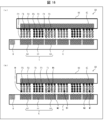
- FIG. 16 is a sectional side view of the light emitting device LD according to the present embodiment.
- the light emitting device LD shown in FIG. 16A is obtained by forming the counter substrate CC on the fifth layer F5 of the substrate C described above.
- the counter substrate CC has a single common electrode CE as a substrate electrode.
- the common electrode CE is formed on the counter substrate CC so as to be exposed on one surface of the counter substrate CC.
- the counter substrate CC and the common electrode CE face each other via the fourth layer F4 to the fifth layer F5 of the substrate C.
- the common electrode CE overlaps all the pixel electrodes E on the substrate C and is in contact with all the fifth layers F5.
- the configuration of the light emitting device LD shown in each drawing of FIG. 16 is an example in this embodiment.
- the common electrode CE may be directly provided on the upper layer of the layer electrodeposited on the substrate C (for example, the upper layer of the fifth layer).
- the common electrode CE and the sealing glass held with a space between the common electrode CE and the common electrode CE are electrodeposited on the substrate C. It may be provided on the upper layer of the layer.
- the first layer F1, the second layer F2, and the third layer F3 may be a blue light emitting layer, a green light emitting layer, and a red light emitting layer, respectively.
- each of the fourth layer F4 and the fifth layer F5 may be a hole transport layer or an electron transport layer.
- the blue light emitting element is arranged at a position overlapping with the first layer F1
- the green light emitting element is arranged at a position overlapping with the second layer F2
- the third layer is formed.
- the light emitting device may include a red light emitting element at a position overlapping with F3.
- the light emitting device LD may function as a display device by providing the blue light emitting element in the blue sub pixel, the green light emitting element in the green sub pixel, and the red light emitting element in the red sub pixel.
- Either one of the substrate C and the counter substrate CC may be a transparent substrate provided with a transparent electrode.
- the light emitting device LD may take out the light from each light emitting element from the transparent substrate side.
- the light emission of each light emitting element may be realized by driving each pixel electrode E.
- the electrodeposition tank connection electrode D may function as a terminal for inputting a signal for driving each pixel electrode E.
- each of the first layer F1, the second layer F2, and the third layer F3 has a first particle M1, a second particle M2, And it is preferable that it consists of only the third particles M3.
- the first particles M1 are formed in the second layer F2 and the first particles M1 are formed in the third layer F3.
- the second particles M2 may be contained in a small amount.
- the first particles M1 in the second layer F2 tend to be formed on the pixel electrode E side in the second layer F2, as shown in (b) of FIG. This is because immediately before the second film forming step, the remaining first particles M1 have already migrated to the pixel electrode E side in the electrodeposition tank 4, so that in the subsequent second film forming step, This is because one particle M1 tends to be preferentially adsorbed. For the same reason, the first particles M1 and the second particles M2 in the third layer F3 tend to be formed on the pixel electrode E side in the third layer F3, as shown in (b) of FIG. ..
- the light emission of the light emitting device is near the interface of the light emitting layer on the hole transporting layer side. Tend to occur in. This is because when the light emitting layer is composed of quantum dots, the mobility of holes in the light emitting layer is lower than the mobility of electrons in the light emitting layer.
- the pixel electrode E of the substrate C is the cathode of the light emitting element described above, and the common electrode CE of the counter substrate CC is the anode of the light emitting element described above.
- the fourth layer F4 function as an electron transport layer and the fifth layer F5 function as a hole transport layer.
- the first particles M1 in the second layer F2 and the first particles M1 and the second particles M2 in the third layer F3 are on the fourth layer F4 of each layer, that is, on the electron transport layer side. It is easily formed. Therefore, even when each light emitting element of the light emitting device LD is driven, the first particles M1 in the second layer F2 and the first particles M1 and the second particles M2 in the third layer F3 emit light. Hard to do. Therefore, so-called color mixing, in which different light is emitted from the light emitting element that emits light of a specific color, is reduced, and display quality is improved.
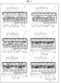
- FIG. 17 is a process cross-sectional view of the light-emitting device manufacturing apparatus 2 and the substrate C for explaining an example of the manufacturing method using the light-emitting device manufacturing apparatus 2 according to the present embodiment. 17 is an enlarged side view of the vicinity of the electrodeposition tank 4 in the electrodeposition process of this embodiment.
- the light emitting device manufacturing apparatus 2 and the substrate C in the present embodiment have the same configurations as the light emitting device manufacturing apparatus 2 and the substrate C in the previous embodiment, respectively.
- the method for manufacturing the light emitting device according to the present embodiment can be realized by the same method as the method for manufacturing the light emitting device according to the previous embodiment, except for steps S24 and S26 in each step of the flowchart shown in FIG. ..
- An example of performing film formation by electrodeposition on the pixel electrodes E of the substrate C using the light emitting device manufacturing apparatus 2 according to this embodiment will be described with reference to FIGS. 14 and 17.
- step S2 the substrate C is installed in the light emitting device manufacturing apparatus 2 (step S2).
- step S2 is executed as in the previous embodiment.
- the electrodeposition solution L1, the electrodeposition solution L2, and the electrodeposition solution L2 are placed in the interior 4A.
- An electrodeposition liquid L4 different from L3 is filled.
- the electrodeposition liquid L4 may contain the same solvent as the solvent of the electrodeposition liquid L1, the electrodeposition liquid L2, and the electrodeposition liquid L3.
- the electrodeposition liquid L4 contains, as functional particles, the first particles M1, the second particles M2, and the third particles M3 described in the previous embodiment.
- the electrodeposition liquid L4 includes fourth particles M4A, fourth particles M4B, and fourth particles M4C instead of the fourth particles M4, and instead of the fifth particles M5, as compared with the electrodeposition liquid L3. , Fifth particles M5A, fifth particles M5B, and fifth particles M5C.
- the fourth particles M4A, the fourth particles M4B, the fourth particles M4C, the fifth particles M5A, the fifth particles M5B, and the fifth particles M5C may have the same configuration as the functional particles up to the previous embodiment, In particular, they have the same polarity.
- the absolute values of the threshold voltages of the fourth particles M4A, the fourth particles M4B, and the fourth particles M4C are smaller than the absolute values of the threshold voltages of the first particles M1 and are different from each other.
- the absolute values of the threshold voltages of the fifth particles M5A, the fifth particles M5B, and the fifth particles M5C are larger than the absolute values of the threshold voltages of the third particles M3, and are different from each other.
- the absolute value of the threshold voltage of the fourth particles M4B is larger than the absolute value of the threshold voltage of the fourth particles M4A and smaller than the absolute value of the threshold voltage of the fourth particles M4C.
- the absolute value of the threshold voltage of the fifth particles M5B is larger than the absolute value of the threshold voltage of the fifth particles M5A and smaller than the absolute value of the threshold voltage of the fifth particles M5C.
- step S4 the pressurizing unit 10 is controlled to press the substrate C against the electrodeposition tank 4, and the substrate holding step is performed (step S4).
- the pixel electrode E on the substrate C is immersed in the electrodeposition liquid L3.
- an electrodeposition step is performed.
- step S24 first, a voltage whose absolute value is larger than the absolute value of the threshold voltage of the fourth particles M4A and smaller than the absolute value of the threshold voltage of the fourth particles M4B is set as the bottom electrode 8.
- the voltage is applied to the first pixel electrode E1.
- FIG. 17A only the fourth particles M4A migrate to each of the first pixel electrodes E1 and are adsorbed on the first pixel electrodes E1.
- the fourth layer F4A containing the fourth particles M4A shown in FIG. 17B is formed on the first pixel electrode E1.
- the voltage application is performed until almost all of the fourth particles M4A in the electrodeposition tank 4 are adsorbed on the pixel electrode E for forming the fourth layer F4A.
- the absolute values of the threshold voltages of the fourth particles M4A, the fourth particles M4B, and the fourth particles M4C are different from each other. Therefore, as described above, the fourth layer F4A can be formed by adsorbing only the fourth particles M4A only on the first pixel electrode E1.
- the fourth layer F4B containing the fourth particles M4B can be formed on the second pixel electrode E2 as shown in (c) of FIG. Further, by applying the same method to the fourth particles M4C, as shown in FIG. 17C, the fourth layer F4C including the fourth particles M4C is separately formed on the third pixel electrode E3. can do. As a result, the fourth layer F4 including the fourth layer F4A, the fourth layer F4B, and the fourth layer F4C shown in (c) of FIG. 17 is provided on different pixel electrodes E, respectively.
- Step S16, Step S18, and Step S20 are carried out in the same manner as in the previous embodiment to form the first layer F1, the second layer F2, and the third layer F3 shown in FIG. 17D. ..
- the first layer F1 is placed on the fourth layer F4A
- the second layer F2 is placed on the fourth layer F4B
- the third layer F3 is placed on the fourth layer F4B.
- a film is formed on the four-layer F4C.
- step S26 first, a voltage whose absolute value is larger than the absolute value of the threshold voltage of the fifth particles M5A and smaller than the absolute value of the threshold voltage of the fifth particles M5B is set to the bottom surface.
- the voltage is applied between the electrode 8 and the first pixel electrode E1.
- the fifth layer F5A including the fifth particles M5A shown in (f) of FIG. 17 is formed on the first layer F1.
- the voltage application is performed until almost all of the fifth particles M5A in the electrodeposition tank 4 are adsorbed on the pixel electrode E for forming the fifth layer F5A.
- the absolute values of the threshold voltages of the fifth particles M5A, the fifth particles M5B, and the fifth particles M5C are different from each other. Therefore, as described above, the fifth layer F5A can be formed by adsorbing only the fifth particles M5A only on the first layer F1.
- the fifth layer F5B including the fifth particles M5B can be formed in the second layer F2 as shown in (f) of FIG. Further, by applying the same method to the fifth particles M5C, as shown in (f) of FIG. 17, the fifth layer F5C including the fifth particles M5C is separately formed on the third layer F3. be able to.
- the fifth layer F5A, the fifth layer F5B, and the fifth layer F5C shown in (f) of FIG. 17 are provided on the first layer F1, the second layer F2, and the third layer F3, respectively.
- the fifth layer F5 is obtained.
- step S22, step S12, and step S14 are performed in the same manner as in the previous embodiment.
- the substrates C individually formed at the positions overlapping the pixel electrodes E are also formed for the fourth layer F4 and the fifth layer F5. can get.
- FIG. 18 is a sectional side view of the light emitting device LD according to this embodiment.
- the light emitting device LD shown in FIG. 18 is obtained by forming the counter substrate CC on the fifth layer F5 of the substrate C described above.
- the counter substrate CC has the same configuration as the counter substrate CC in the previous embodiment.
- the light emitting device LD in the present embodiment is individually formed for each pixel electrode E in the fourth layer F4 and the fifth layer F5 as compared with the light emitting device LD in the previous embodiment. Therefore, the functional particles contained in the fourth layer F4 with which the first layer F1, the second layer F2, and the third layer F3 are in contact are different from each other. Similarly, the functional particles contained in the fifth layer F5 with which the first layer F1, the second layer F2, and the third layer F3 are in contact are different from each other.
- the fourth layer F4 and the fifth layer F5 suitable for the first layer F1, the second layer F2, and the third layer F3 can be individually formed.
- the first layer F1, the second layer F2, and the third layer F3 of the light emitting device LD according to the present embodiment are light emitting layers that emit light of different colors, respectively, a hole transport layer suitable for the respective light emitting layers and The electron transport layer may be different for each color emitted.
- the fourth layer F4 is an electron transport layer and the fifth layer F5 is a hole transport layer
- an appropriate electron transport layer and hole transport layer are separately formed for each color to be emitted. be able to. Therefore, according to the manufacturing method of the present embodiment, it is possible to provide the light emitting device LD including the light emitting element with further improved light emitting efficiency.
- the sixth voltage may be applied between the bottom electrode 8 and the second pixel electrode E2 and the third pixel electrode E3 that do not adsorb the first particles M1. Good.
- the absolute value of the sixth voltage is smaller than the absolute value of the first voltage.
- the first particles M1 migrate toward the first pixel electrode E1 also by the electric field generated between the second pixel electrode E2 and the third pixel electrode E3 and the first pixel electrode E1. Therefore, the film formation rate of the first layer F1 on the first pixel electrode E1 is improved. Since the absolute value of the sixth voltage is smaller than the absolute value of the first voltage, adsorption of the first particles M1 by the second pixel electrode E2 or the third pixel electrode E3 is reduced.
- the sixth voltage may have a polarity opposite to that of the first voltage.
- the seventh voltage is applied between the bottom electrode 8 and the first pixel electrode E1 and the third pixel electrode E3 that do not adsorb the second particles M2. Good.
- the absolute value of the seventh voltage is smaller than the absolute value of the second voltage.
- the second particles M2 migrate toward the second pixel electrode E2 also by the electric field generated between the first pixel electrode E1 and the third pixel electrode E3 and the second pixel electrode E2. Therefore, the film formation rate of the second layer F2 on the second pixel electrode E2 is improved. Since the absolute value of the seventh voltage is smaller than the absolute value of the second voltage, the adsorption of the second particles M2 by the first pixel electrode E1 or the third pixel electrode E3 is reduced.
- the seventh voltage may have a polarity opposite to that of the second voltage.
Landscapes
- Engineering & Computer Science (AREA)
- Manufacturing & Machinery (AREA)
- Electroluminescent Light Sources (AREA)
Abstract
基板(C)に形成された基板電極(U)に対する、機能粒子(M1・M2)の電着を行う発光デバイスの製造方法であって、第1成膜工程と、該第1成膜工程に次ぐ第2成膜工程とを備える。前記第1成膜工程において、前記基板電極の内の第1基板電極と、対向電極(8)との間に、第1電圧を印加し、第1粒子(M1)を前記第1基板電極に成膜する。前記第2成膜工程において、前記基板電極の内の第2基板電極と、前記対向電極との間に、第2電圧を印加し、第2粒子(M2)を前記第2基板電極に成膜する。前記第1電圧の絶対値は、前記第2電圧の絶対値よりも小さい。
Description
本発明は、発光デバイスの機能層を電着により形成する、発光デバイスの製造方法に関する。
特許文献1には、有機発光素子の製造において、有機発光層を電着法によって形成する方法が開示されている。
特許文献1に記載の技術においては、互いに異なる材料を含む、複数の層を形成する場合には、当該層を形成するごとに電着液の変更を行う必要がある。このために、タクトタイムの増加が問題となる。
上記課題を解決するために、本発明の発光デバイスの製造方法は、基板に形成された基板電極に対する、機能粒子の電着を行う発光デバイスの製造方法であって、前記基板と、該基板に平行に配置された対向電極との間において、第1粒子と、当該第1粒子と異なる第2粒子とを、前記機能粒子として含む電着液を挟持する基板把持工程と、前記基板把持工程の後、前記基板電極の内の第1基板電極と、前記対向電極との間に、第1電圧を印加し、前記第1粒子を前記第1基板電極に成膜する第1成膜工程と、前記第1成膜工程に次いで、前記基板電極の内の第2基板電極と、前記対向電極との間に、第2電圧を印加し、前記第2粒子を前記第2基板電極に成膜する第2成膜工程とを備え、前記第1電圧の絶対値が、前記第2電圧の絶対値よりも小さい。
上記構成により、発光デバイスの製造におけるタクトタイムを短縮できる。
〔実施形態1〕
本実施形態においては、図2に示す基板Cに対して電着を実施するための製造装置および製造方法について説明を行う。図2は、本実施形態に係る基板Cの概略斜視図である。図2に示すように、基板Cは、基板電極として、単一の平面電極Uと、電着槽接続用電極Dとを備える。
本実施形態においては、図2に示す基板Cに対して電着を実施するための製造装置および製造方法について説明を行う。図2は、本実施形態に係る基板Cの概略斜視図である。図2に示すように、基板Cは、基板電極として、単一の平面電極Uと、電着槽接続用電極Dとを備える。
平面電極Uは、基板Cの何れか一方の面上において露出するように、基板Cに形成されている。例えば、平面電極Uは、基板C上において、矩形状に形成されている。
電着槽接続用電極Dは、基板Cの平面電極Uが形成された面上において、基板Cの互いに直交する何れか2辺に沿って形成される。平面電極Uと電着槽接続用電極Dとは電気的に導通しているため、電着槽接続用電極Dに電圧を印加することにより、平面電極Uに電圧を印加することができる。なお、電着槽接続用電極Dは、基板Cの平面電極Uが形成された面上に形成されている限り、基板Cの直交する2辺に沿って形成される構成のみならず、基板Cの何れか1辺に沿ってのみ設けられる等、形状は特に限られない。
平面電極Uおよび電着槽接続用電極Dは、基板Cの平面電極Uおよび電着槽接続用電極Dが形成された面と面一であり、当該面において露出している。
図3は、本実施形態に係る発光デバイスの製造装置2の概略図である。図3の(a)は、発光デバイスの製造装置2の斜視図である。図3の(b)は、発光デバイスの製造装置2の上面図である。図3の(c)は、図3の(b)における、A-A線矢視断面図である。なお、図3の(a)においては、基板Cが発光デバイスの製造装置2に設置された様子を図示する。しかしながら、図示の簡単のために、図3の(b)および図3の(c)においては、基板Cの図示を省略している。
また、本明細書において、各図の発光デバイスの製造装置2の上面図は、特に断りの無い限り、図3の(b)に対応する位置における上面図を示すものとする。さらに、本明細書において、各図の発光デバイスの製造装置2の断面図は、特に断りの無い限り、図3の(c)に対応する位置における断面図を示すものとする。
図3に示すように、本実施形態に係る発光デバイスの製造装置2は、電着槽4と、底面電極8と、加圧部10と、電着電源12とを備える。
電着槽4は、電着槽4の外形を規定する外側面14と、電着槽4の内部4Aを規定する内側面16および底面18を含む。外側面14と内側面16との間には、縁部20が規定される。縁部20の上面には、複数の基板接続用電極22が形成されている。すなわち、電着槽4の外周には、複数の基板接続用電極22が形成されている。
底面電極8は、電着槽4の底面18に形成されている。底面電極8は、底面18と面一であり、かつ、底面18から露出している。さらに、発光デバイスの製造装置2に基板Cが設置された際に、底面電極8は、基板Cに形成された平面電極Uと向かい合う対向電極となる。
加圧部10は、基板Cと電着槽4との少なくとも一方を移動させて、基板Cと電着槽4との相対距離を制御する機構を有する。本実施形態においては、基板Cを加圧部10に配置することにより、発光デバイスの製造装置2への基板Cの設置が実施されるとする。基板Cを加圧部10に配置する際、基板Cの平面電極Uが、電着槽4の底面電極8と、平行に向かい合うように、基板Cを配置する。
加圧部10としては、例えば、基板Cを把持する真空チャックであってもよい。この場合、加圧部10は、基板Cを電着槽4に対して移動させることにより、基板Cと電着槽4との相対距離を制御してもよい。
加圧部10は、基板Cと電着槽4と接近させて、互いに接触させる位置まで、基板Cと電着槽4とを互いに近接させることができる。基板Cと電着槽4とが互いに押し付けられた状態における、図3の(a)および図3の(c)に対応する概略図を、図4の(a)および図4の(b)にそれぞれ示す。なお、図4の(b)については、基板Cの断面についても図示をしている。
基板Cと電着槽4とが互いに押し付けられた際、図4の(b)に示すように、底面電極8は、内部4Aを介して、基板Cの平面電極Uと対向する。すなわち、基板Cと電着槽4とが互いに押し付けられた状態においては、基板Cと、基板Cと平行である底面電極8との間において、内部4Aを挟持する。
また、基板Cと電着槽4とが互いに押し付けられた際、図4の(b)に示すように、電着槽4の基板接続用電極22と、基板Cの電着槽接続用電極Dとが接触し、互いに電気的に導通する。なお、図3の(c)および図4の(b)に示すように、電着槽4は、基板接続用電極22と、電着槽接続用電極Dとの電気的導通を補助するために、基板接続用電極22を押し上げるバネ38を、各基板接続用電極22の下部に備えていてもよい。
ここで、図3の(c)に示すように、側面16と底面18とにより規定された、内部4Aは、縁部20の上面から底面電極8の上面までの距離d1を有する。この距離d1は、内部4Aの深さに相当し、図4の(b)に示すように、基板Cと電着槽4とが互いに押し付けられた際の、底面電極8と平面電極Uとの間の距離と、実質的に一致する。
電着電源12は、底面電極8と基板接続用電極22とに対して、少なくとも2値の電圧を印加する電源である。さらに、電着電源12は、基板接続用電極22および電着槽接続電極Dを介して、基板Cの平面電極Uに対しても電圧を印加してもよい。したがって、電着電源12は、平面電極Uと底面電極8との間に、少なくとも2値の電圧を印加してもよい。
ここで、基板Cと電着槽4とが互いに押し付けられた際、基板接続用電極22および電着槽接続電極Dを介した、平面電極Uに対する電圧印加が可能である限り、基板接続用電極22の形状についても、特に限定されない。例えば、電着槽接続電極Dが基板Cの1辺に沿って形成さえている場合、基板接続用電極22は、基板Cと電着槽4とが互いに押し付けられた際、電着槽接続電極Dと重畳する、縁部20の上面の内の1辺に沿って形成されていてもよい。
本実施形態に係る発光デバイスの製造装置2を用いて、基板Cの平面電極U上に電着による成膜を実行する一例について、図5および図1を参照して説明する。図5は、本実施形態に係る発光デバイスの製造装置2を用いた製造方法の一例を説明するためのフローチャートである。図1は、図5に示す製造方法における、発光デバイスの製造装置2および基板Cの工程断面図である。
本実施形態に係る発光デバイスの製造方法においては、はじめに、図1の(a)に示すように、発光デバイスの製造装置2に基板Cを設置する(ステップS2)。ステップS2は、例えば、基板Cの平面電極Uが底面電極8と向かい合うように、基板Cを加圧部10に設置することにより実行される。本実施形態においては、ステップS2において加圧部10に設置された基板Cを、電着槽4に近接させる前に、内部4Aに電着液L1が充填されている。
本実施形態において、電着液L1は、複数の機能粒子を含む。電着液L1が含む機能粒子は、溶媒である電着液L1中に分散されている。電着液L1としては、例えば、水、アルキルアルコール、トルエン、プロピレングリコールモノメチルエーテルアセテート(PGMEA)、またはアルカン等が挙げられる。
電着液L1が含む機能粒子は、例えば、発光素子の機能層の材料であってもよい。発光素子の機能層としては、例えば、発光素子の電極間に形成される、電子輸送層、発光層、または正孔輸送層が挙げられる。特に、機能粒子が、発光層の材料である場合は、当該機能粒子は、自発光粒子であってもよい。本実施形態における機能粒子は、無機ナノ粒子を含んでいてもよく、特に、半導体ナノ粒子、すなわち、量子ドットを含んでいてもよい。
本実施形態における機能粒子が、発光層のナノ粒子材料である場合は、当該機能粒子が、CdSe、ZnSe、またはInP等からなる、単一コア構造を備えていてもよい。また、本実施形態における機能粒子は、CdSe/ZnS、InP/ZnS、CdSe/CdS、またはZnSe/ZnS等からなる、コア/シェル構造を備えていてもよい。また、本実施形態における機能粒子は、CdSe/ZnSe/ZnS等からなる、マルチシェル構造を備えていてもよい。
本実施形態における機能粒子が、電子輸送層のナノ粒子材料である場合は、当該機能粒子が、ZnO、ZrO、MgZnO、AlZnO、TiO2、Ta2O3、またはSrTiO3等を含んでいてもよい。本実施形態における機能粒子が、正孔輸送層のナノ粒子材料である場合は、当該機能粒子が、NiO、CuI、Cu2O、CoO、Cr2O3、またはMoO3等を含んでいてもよい。
さらに、本実施形態において、電着液L1は、図1の(a)に示すように、機能粒子として、互いに異なる粒子である、第1粒子M1と第2粒子M2とを含む。特に、第1粒子M1と第2粒子M2とが、発光層の材料である場合は、第1粒子M1と第2粒子M2とは、互いに異なる光を発する自発光粒子であってもよい。
本実施形態において、電着液L1が含む機能粒子は、当該機能粒子のそれぞれに配位結合する配位子を備えていてもよい。例えば、図6の(a)に示すように、第1粒子M1は、周囲に第1配位子R1が配位した構造を有していてもよく、第2粒子M2は、周囲に、第1配位子R1とは異なる第2配位子R2が配位した構造を有していてもよい。本実施形態における配位子としては、例えば、メルカプトアルカン酸、アルカンチオール、アルキルアミン、アルカン、アルケン、トリオクチルホスフィン(TOP)、または酸化トリオクチルホスフィン(TOPO)等が挙げられる。
次いで、加圧部10を制御して、基板Cを電着槽4に押し付ける(ステップS4)。ステップS4の実行により、図1の(b)に示すように、基板Cの平面電極Uが形成された面と、縁部20の上面とが当接する。これにより、内部4Aに充填された電着液L1を、基板Cと、基板Cと平行である底面電極8との間において挟持する、基板把持工程を実施する。
この際、基板Cから露出した平面電極Uの表面は、内部4Aの電着液L1に浸漬される。このため、電着液L1は、内部4Aが満たされ、内部4Aの電着液L1の液面が、表面張力により、縁部20の上面よりも若干高くなるように、内部4Aに充填される。これにより、基板Cの平面電極Uが形成された面が面一であったとしても、当該面が縁部20の上面と当接した際、平面電極Uの表面が電着液L1に浸漬される。
また、ステップS4において、確実に平面電極Uの表面を電着液L1に浸漬するために、ステップS4において縁部20と当接する部分のみ、基板Cを薄く形成してもよい。当該構成であれば、基板Cと縁部20と当接した際、平面電極Uの表面が縁部20の上面よりも内部4Aに入り込むため、より確実に平面電極Uの表面が電着液L1に浸漬される。
なお、ステップS4により、基板Cが縁部20の上面に押し付けられるため、図1の(b)に示すように、基板Cに形成された電着槽接続用電極Dと、縁部20の上面から露出する基板接続用電極22とが当接し、電気的に導通する。
ステップS4に次いで、電着工程を実施する。
本実施形態において、第1粒子M1と第2粒子M2とは、特定の官能基を備えることにより、極性を有している。このため、電着工程においては、底面電極8と平面電極Uとの間に生じる電界によって、第1粒子M1と第2粒子M2とが、クーロン相互作用により、電着液L1中を泳動する。さらに、第1粒子M1と第2粒子M2とは、同じ極性を有している。本実施形態においては、電着工程において、第1粒子M1と第2粒子M2とが、平面電極Uに向かって泳動するように、各電極に印加される電圧が制御される。
また、第1粒子M1と第2粒子M2とのそれぞれは、平面電極Uに吸着され、平面電極Uに成膜されるために必要な、底面電極8と平面電極Uとの間の閾値電圧がそれぞれ異なっている。各機能粒子に対する閾値電圧は、当該機能粒子の粒径、配位する配位子の種類、または、当該機能粒子1つに配位する配位の個数によって異なる。
本実施形態においては、第1粒子M1に対する閾値電圧である、第1閾値電圧V1の絶対値が、第2粒子M2に対する閾値電圧である、第2閾値電圧V2の絶対値よりも低い。すなわち、第1粒子M1は、第2粒子M2と比較して、より小さな底面電極8と平面電極Uとの間の電界下において、平面電極Uに吸着され、成膜される。
本実施形態は、電着工程において、はじめに、絶対値が、第1閾値電圧V1の絶対値以上であり、かつ、第2閾値電圧V2の絶対値未満である、第1電圧を、底面電極8と平面電極Uとの間に印加する、第1成膜工程を実施する(ステップS6)。ステップS6においては、図1の(c)に示すように、電着液L1に含まれる機能粒子のうち、第1粒子M1のみが平面電極Uに泳動し、平面電極U上に吸着される。
ステップS6における電圧印加を十分におこなうことにより、平面電極U上に、図1の(c)に示す、第1粒子M1を含む第1層F1が成膜される。なお、ステップS6は、電着槽4中の第1粒子M1のほぼ全てが、第1層F1の成膜のために、平面電極U上に吸着されるまで実施される。
ステップS6に次いで、絶対値が、第2閾値電圧V2の絶対値以上である、第2電圧を、底面電極8と平面電極Uとの間に印加する、第2成膜工程を実施する(ステップS8)。ステップS8においては、第2粒子M2についても平面電極Uに泳動し、平面電極U上に吸着される。ステップS8における電圧印加を十分におこなうことにより、第1層F1上に、図1の(d)に示す、第2粒子M2を含む第2層F2が成膜される。
ステップS6において、電着槽4中の第1粒子M1はほぼ全て消費されているため、ステップS8において、第2層F2中に第1粒子M1が混在することを低減できる。なお、第2層F2中の第1粒子M1の密度が、最終的な発光デバイスとしての不良の基準を下回る限りは、第2層F2に微量の第1粒子M1が含まれていてもよい。したがって、本実施形態においては、ステップS8において、微量の第1粒子M1が電着槽4中に含まれていてもよい。
なお、本実施形態においては、電着液L1に含まれる機能材料が有する極性が、負極性である場合を例示している。すなわち、底面電極8には負の極性の電圧を印加し、平面電極Uには正の極性の電圧を印加している。なお、電着液L1に含まれる機能材料が有する極性が逆転した場合、各電極に印加する電圧の極性についても逆転させればよい。
次いで、底面電極8と平面電極Uとの間の電圧印加を解除し(ステップS10)、電着工程を完了する。次いで、図1の(e)に示すように、電着槽4から基板Cを引き上げる(ステップS12)。ステップS12は、加圧部10を制御して、基板Cを電着槽4から引き離すことにより実行される。次いで、加圧部10から基板Cを取り外す(ステップS14)ことにより、下層から、第1層F1および第2層F2を、平面電極U上に積層して備えた基板Cを得る。この後、第2層F2の上層に、対向基板等を形成することにより、発光デバイスを製造してもよい。
本実施形態においては、互いに異なる機能粒子の電着を、電着液の交換または電着槽の交換なく実施することが可能である。このため、互いに異なる機能材料をそれぞれ含む複数の層を形成する場合であっても、タクトタイムを低減することができる。
また、本実施形態においては、底面電極8との間に第1電圧を印加する電極である第1基板電極と、底面電極8との間に第2電圧を印加する電極である第2基板電極とが、同一の平面電極Uである場合を説明した。本実施形態によれば、互いに異なる機能材料をそれぞれ含む複数の層を、同一の平面電極U上に積層して形成することができる。
なお、電着液L1の第1粒子M1と第2粒子M2との混合は、ステップS6、すなわち、第1成膜工程の直前において実行されることが好ましい。第1粒子M1と第2粒子M2とが混合されてから長時間が経過した場合、第1粒子M1と第2粒子M2との間において、配位子の吸脱着が発生する場合がある。これは、第1粒子M1と第2粒子M2との間において、平衡論的に配位子の移動が発生するためである。このため、第1粒子M1と第2粒子M2とが混合されてから長時間が経過した場合、図6の(b)に示すように、第1粒子M1においても、第2粒子M2においても、第1配位子R1と第2配位子R2との両方が配位した状態に変化する場合がある。
電着液L1の第1粒子M1と第2粒子M2との混合が第1成膜工程の直前において実行されることにより、上述した配位子の平衡化が生じにくくなる。このため、電着液L1における、第1粒子M1と第2粒子M2とのリガンド組成がより明確に異なるため、第1粒子M1と第2粒子M2との特性をより明確に異ならせることができる。したがって、第1閾値電圧V1と第2閾値電圧V2とのそれぞれの絶対値についても、より明確に異ならせることができ、結果として、各機能粒子の成膜の歩留まりが向上する。具体的には、第1粒子M1と第2粒子M2との混合は、例えば、電着槽4への電着液L1の充填に併せて実行されてもよい。
なお、本明細書における「電着」とは、溶液中において二電極間に電位差を生じさせることにより、当該溶液中の材料からなる薄膜を成膜する電気化学的成膜方法を含んでいる。本明細書における「電着」は、例えば、電着法、電着塗装法、電気泳動堆積法、誘電泳動堆積法、ミセル電解法、電気めっき法、電鋳、などの手法を含んでいてもよい。これらの何れかの手法を、上述の電着工程として選択した場合であっても、上述した効果を奏する発光デバイスを製造できる。
〔変形例〕
本実施形態における変形例について、図7を参照して詳細に説明する。図7の(a)から図7の(c)は、ステップS6における、底面電極8と平面電極Uとの間に印加される電圧を縦軸、当該電圧の印加開始からの経過時間を横軸にとって図示したグラフである。
本実施形態における変形例について、図7を参照して詳細に説明する。図7の(a)から図7の(c)は、ステップS6における、底面電極8と平面電極Uとの間に印加される電圧を縦軸、当該電圧の印加開始からの経過時間を横軸にとって図示したグラフである。
ステップS6における電圧の印加は、例えば、図7の(a)のグラフに示すように、底面電極8と平面電極Uとの間に、常時第1閾値電圧以上、かつ第2閾値電圧V2未満の第1電圧を印加し続けることにより実現してもよい。
しかしながら、本実施形態の変形例においては、これに限られず、ステップS6における電圧の印加は、図7の(b)に示すように、底面電極8と平面電極Uとの間に、第1電圧と、逆電圧VR(第8電圧)とを交互に印加することにより実現してもよい。すなわち、ステップS6は、底面電極8と平面電極Uとの間に、第1電圧を印加する順電圧印加工程と、逆電圧VRを印加する逆電圧印加工程とを、交互に実行することにより実現してもよい。
逆電圧VRは、第1閾値電圧V1とは極性が逆の電圧である。逆電圧VRの絶対値は、図7の(b)に示すように、第1閾値電圧V1よりも小さい。なお、ステップS6においては、図7の(b)にも示すように、第1電圧を印加する順電圧印加工程の期間よりも、逆電圧VRを印加する逆電圧印加工程の期間の方が短くてもよい。
ステップS6において、図7の(a)のグラフに示すように、底面電極8と平面電極Uとの間に、常時第1電圧を印加し続けた場合、第1粒子M1は常時平面電極側に泳動し続けることとなる。さらに、第2粒子M2は、平面電極Uに吸着はされないものの、平面電極Uの方向に泳動はするため、電着槽4中の平面電極U側においては、第2粒子M2の密度も上昇している。
このため、第1粒子M1に捲き込まれた第2粒子M2が、第1粒子M1に抑えつけられるように平面電極Uに吸着される場合がある。したがって、上述した場合には、図8に示す、ステップS6完了時点における発光デバイスの製造装置2の工程断面図に示すように、第1層F1中に、第2粒子M2が微量に析出する場合がある。
ステップS6において、図7の(b)のグラフに示すように、順電圧印加工程と逆電圧印加工程とを、交互に実行することにより、逆電圧印加工程においては、第1粒子M1と第2粒子M2とが、底面電極8に向かって泳動する。このため、第1粒子M1と第2粒子M2とが、底面電極8側への泳動と、平面電極U側への泳動とを繰り返す。順電圧印加工程においては第1電圧を印加しているため、第1粒子M1は、底面電極8側への泳動と、平面電極U側への泳動とを繰り返す間に、次第に平面電極Uに接近し、最終的には平面電極Uに吸着する。
第1粒子と第2粒子とが、底面電極8側への泳動と、平面電極U側への泳動とを繰り返すために、第2粒子M2が、第1粒子M1に抑えつけられるように平面電極Uに吸着される可能性が低減される。ゆえに、第1層F1中に第2粒子M2が含まれるような成膜不良の発生を低減できる。なお、逆電圧VRの絶対値は、第1電圧V1の絶対値よりも小さいため、第1粒子M1が底面電極8に吸着されることを低減できる。
なお、順電圧印加工程と逆電圧印加工程とを、交互に実行する手法は、図7の(b)のグラフに示すように、第1電圧と逆電圧VRとを交互に印加する手法に限らない。例えば、図7の(c)に示すように、底面電極8と平面電極Uとの間の電圧が、経過時間を横軸として、正弦波を描くように、電圧印加を実施してもよい。この場合、当該正弦波の最大値が第1電圧であってもよく、最小値が逆電圧VRであってもよい。この場合においても、上述した効果が同様に得られる。なお、他の例として、底面電極8と平面電極Uとの間の電圧は、経過時間を横軸として、疑似正弦波または三角波を描いていてもよい。
〔実施形態2〕
本実施形態以降においては、図9に示す基板Cに対して電着を実施するための製造装置および製造方法について説明を行う。図9は、本実施形態に係る基板Cの概略斜視図である。図9に示す基板Cは、図1に示す基板Cと比較して、平面電極Uに代えて複数の画素電極Eを備え、電着槽接続用電極Dを複数備える点においてのみ構成が異なる。
本実施形態以降においては、図9に示す基板Cに対して電着を実施するための製造装置および製造方法について説明を行う。図9は、本実施形態に係る基板Cの概略斜視図である。図9に示す基板Cは、図1に示す基板Cと比較して、平面電極Uに代えて複数の画素電極Eを備え、電着槽接続用電極Dを複数備える点においてのみ構成が異なる。
画素電極Eは、基板Cの何れか一方の面上において露出するように、基板Cにパターン形成されている。例えば、画素電極Eは、基板C上において、マトリクス状に形成されている。
電着槽接続用電極Dは、基板Cの画素電極Eが形成された面上において、基板Cの互いに直交する何れか2辺に沿って複数形成される。個々の電着槽接続用電極Dに電圧を印加することにより、個々の画素電極Eに電圧を印加することができる。このため、基板Cには、各画素電極Eと接続する、図示しないトランジスタが複数形成されていてもよく、個々の電着槽接続用電極Dに電圧を印加することにより、各トランジスタを駆動し、個々の画素電極Eに電圧を印加してもよい。
画素電極Eおよび電着槽接続用電極Dは、基板Cの画素電極Eおよび電着槽接続用電極Dが形成された面と面一であり、当該面において露出している。
本実施形態においても、基板Cに対する電着を、発光デバイスの製造装置2を用いて実行する。本実施形態における発光デバイスの製造装置2は、前実施形態における発光デバイスの製造装置2と同一の構成を備えていてもよい。本実施形態における、基板Cと電着槽4とが互いに押し付けられた状態における、図3の(a)および図3の(c)に対応する概略図を、図10の(a)および図10の(b)にそれぞれ示す。
本実施形態においては、基板Cと電着槽4とが互いに押し付けられた際、電着槽4の複数の基板接続用電極22と、基板Cの複数の電着槽接続用電極Dとのそれぞれが接触し、互いに電気的に導通する。電着電源12は、基板接続用電極22および電着槽接続電極Dを介して、基板Cの画素電極Eのそれぞれに対し、個別に電圧を印加することができる。したがって、電着電源12は、個々の画素電極Eと底面電極8との間に、少なくとも2値の電圧を印加する。
本実施形態に係る発光デバイスの製造装置2を用いて、基板Cの画素電極E上に電着による成膜を実行する一例について、図11および図12を参照して説明する。図11は、本実施形態に係る発光デバイスの製造装置2を用いた製造方法の一例を説明するためのフローチャートである。図12は、図11に示す製造方法における、発光デバイスの製造装置2および基板Cの工程断面図である。図12の各図においては、本実施形態の電着工程における、電着槽4近傍の拡大側面図を示す。
本実施形態において、基板Cは、図12の各図に示すように、画素電極Eとして、第1画素電極E1と、第2画素電極E2と、第3画素電極E3とを、それぞれ複数備えている。本実施形態においては、第1画素電極E1と、第2画素電極E2と、第3画素電極E3とのそれぞれに、互いに異なる機能粒子からなる層を成膜する方法を説明する。
本実施形態に係る発光デバイスの製造方法においては、はじめに、発光デバイスの製造装置2に基板Cを設置する(ステップS2)。ステップS2は、前実施形態と同様に実行される。ただし、本実施形態においては、ステップS2において加圧部10に設置された基板Cを、電着槽4に近接させる前に、内部4Aに電着液L1と異なる電着液L2が充填されている。
電着液L2は、電着液L1の溶媒と同一の溶媒を含んでいてもよい。電着液L2は、機能粒子として、前実施形態において説明した、第1粒子M1および第2粒子M2に加えて、第3粒子M3を含む。第3粒子M3は、第1粒子M1および第2粒子M2と同様に、発光素子の機能層の材料であってもよく、半導体ナノ粒子、すなわち、量子ドットであってもよい。
本実施形態においても、第3粒子M3は、第1粒子M1と第2粒子M2と同じ極性を有している。本実施形態においても、第1粒子M1と第2粒子M2とが、画素電極Eの何れかに吸着され、当該画素電極Eに成膜されるために必要な、底面電極8と画素電極Eとの間の閾値電圧として、それぞれ、第1閾値電圧V1と第2閾値電圧V2とを有する。また、第3粒子M3が、画素電極Eの何れかに吸着され、当該画素電極Eに成膜されるために必要な閾値電圧である、第3閾値電圧V3の絶対値は、第2閾値電圧V2の絶対値よりも大きい。
次いで、前実施形態と同様に、加圧部10を制御して、基板Cを電着槽4に押し付け、基板把持工程を実施する(ステップS4)。これにより、基板Cの画素電極Eは電着液L2に浸漬される。ステップS4に次いで、電着工程を実施する。
本実施形態は、電着工程において、はじめに、絶対値が、第1閾値電圧V1の絶対値以上であり、かつ、第2閾値電圧V2の絶対値未満である、第1電圧を、底面電極8と第1画素電極E1との間に印加する、第1成膜工程を実施する(ステップS16)。ステップS16においては、図12の(a)に示すように、電着液L2に含まれる機能粒子のうち、第1粒子M1のみが第1画素電極E1に泳動し、第1画素電極E1上に吸着される。
ステップS16における電圧印加を十分におこなうことにより、第1画素電極E1上に、図12の(b)に示す、第1粒子M1を含む第1層F1が成膜される。なお、ステップS16は、電着槽4中の第1粒子M1のほぼ全てが、第1層F1の成膜のために、第1画素電極E1上に吸着されるまで実施される。
ここで、電着工程においては、成膜を行いたい全ての画素電極Eに対し、均一に電圧を印加することが困難である場合がある。特に、特定の画素電極Eにおいて電圧の降下が発生する場合がある。上記について、本実施形態と比較形態とを対比しつつ説明する。
図13の(a)および図13の(b)は、本実施形態に係る発光デバイスの製造装置2を用いた電着工程について説明するための工程断面図である。図13の(c)および図13の(d)は、比較形態に係る発光デバイスの製造装置を用いた電着工程について説明するための工程断面図である。
なお、比較形態に係る発光デバイスの製造装置は、電着槽4の代わりに、距離d1よりも大きい距離d2を深さとして有する、電着槽4Cを備える点を除いて、本実施形態に係る発光デバイスの製造装置2と同一の構成を備える。
ここでは、本実施形態および比較形態において、第1画素電極E1のうち、第1画素電極E1Aに対し、第1画素電極E1Bに印加された電圧が、望ましい電圧よりも降下したとする。この場合、底面電極8と第1画素電極E1Aとの間に生じる電界よりも、底面電極8と第1画素電極E1Bとの間に生じる電界が弱くなる。第1画素電極E1Aと第1画素電極E1Bとのそれぞれに成膜される第1層F1を、それぞれ、第1層F1Aと第1層F1Bとする。この場合、第1層F1Aの成膜速度よりも、第1層F1Bの成膜速度が遅くなる。
しかしながら、ある特定の画素電極Eの近傍に存在する第1粒子M1が、第1層F1の成膜によって減少することにより、当該画素電極Eに対する第1粒子M1の成膜速度は急激に低下する。ここで、上記成膜工程において、第1層F1Aの成膜速度が比較的速いことにより、第1画素電極E1Aの近傍の第1粒子M1は比較的素早く消費される。また、本実施形態のように、比較的短い距離d1を深さとして有する電着槽4においては、電着槽4中の第1粒子M1の総量が比較的少ない。したがって、上記成膜工程においては、第1画素電極E1Aの近傍の第1粒子M1が急速に少なくなるため、しばらく第1層F1Aの成膜が続いた後、第1層F1Aの成膜速度は急速に低下する。
また、第1層F1Bの成膜速度は比較的遅いため、第1層F1Aの成膜速度が急速に低下した時点においても、まだ第1画素電極E1Bの近傍には第1粒子M1が残存している。このために、さらに時間が経過することにより、第1層F1Bの成膜は、第1層F1Aの成膜が実質的に停止した後も継続する。第1層F1Bの成膜は、第1画素電極E1Bの近傍の第1粒子M1が少なくなるまで続く。
第1粒子M1が電着液L2において略均等に分散しているとすると、各画素電極近傍における第1粒子M1の総量は略同一である。すなわち、成膜に十分に時間をかけた場合、第1層F1Aと第1層F1Bとに含まれる第1粒子M1の量は、実質的に同一となる。したがって、図13の(b)に示すように、第1層F1Aと第1層F1Bとの膜厚をそれぞれ、膜厚dF1と膜厚dF2とおくと、膜厚dF1と膜厚dF2とは略同一の膜厚となる。
ゆえに、本実施形態に係る発光デバイスの製造装置2は、各画素電極Eに対する電圧印加を行った際、特定の画素電極Eにおいて電圧降下等が発生した場合においても、各画素電極Eに成膜された層の膜厚差を低減できる。
一方、比較形態のように、比較的長い距離d2を深さとして有する電着槽4Cにおいては、電着槽4C中の第1粒子M1の総量が比較的多くなる。このために、しばらく第1層F1Aの成膜が続いた後であっても、第1画素電極E1Aの近傍の比較的多くの第1粒子M1が残存している。このため、第1層F1Aの成膜速度は比較的長時間低下せず、継続して第1層F1Aの成膜が実施される。したがって、比較形態においては、電圧を印加している間、第1画素電極E1Bのみならず、第1画素電極E1Aにおいても成膜が継続することとなる。
ゆえに、第1層F1Bと比較して、成膜速度が速い第1層F1Aが急速に成膜されることにより、第1層F1Aの膜厚が第1層F1Bの膜厚と比較して厚くなる。すなわち、図13の(d)に示すように、第1層F1Aと第1層F1Bとの膜厚をそれぞれ、膜厚dFAと膜厚dFBとおくと、膜厚dFAは膜厚dFBよりも厚くなる。
このため、第1層F1Aの膜厚が目標とする第1層F1の膜厚に到達した時点において電圧印加を解除した場合、第1層F1Bの膜厚が目標とする第1層F1の膜厚よりも薄くなる。加えて、第1層F1Bとして成膜されなかった、第1画素電極E1B近傍の第1粒子M1が比較的多く残存することとなる。このため、後工程において、第2画素電極E2または第3画素電極E3に、残存していた第1粒子M1が成膜される場合がある。
本実施形態の成膜工程においては、電着槽4の深さに相当する距離d1を適切に設計し、第1粒子M1が全て消費された場合に、第1層F1の膜厚が目標の膜厚となるように設計すればよい。これにより、第1成膜工程の完了後、電着液L2中の第1粒子M1がほぼ全て消費されるため、上述した膜厚差を低減することが可能である。
ステップS16に次いで、絶対値が、第2閾値電圧V2の絶対値以上であり、かつ、第3閾値電圧V3の絶対値未満である、第2電圧を、底面電極8と第2画素電極E2との間に印加する、第2成膜工程を実施する(ステップS18)。ステップS18においては、図12の(c)に示すように、第2粒子M2と第3粒子M3のうち、第2粒子M2のみが第2画素電極E2に泳動し、第2画素電極E2上に吸着される。ステップS18における電圧印加を十分におこなうことにより、第2画素電極E2上に、図12の(d)に示す、第2粒子M2を含む第2層F2が成膜される。
ステップS16において、電着槽4中の第1粒子M1はほぼ全て消費されているため、ステップS18において、第2層F2中に第1粒子M1が混在することを低減できる。なお、第2層F2中の第1粒子M1の密度が、最終的な発光デバイスとしての不良の基準を下回る限りは、第2層F2に微量の第1粒子M1が含まれていてもよい。したがって、本実施形態においては、ステップS18において、微量の第1粒子M1が電着槽4中に含まれていてもよい。
ステップS18に次いで、絶対値が、第3閾値電圧V3の絶対値以上である、第3電圧を、底面電極8と第3画素電極E3との間に印加する、第3成膜工程を実施する(ステップS20)。ステップS20においては、図12の(e)に示すように、第3粒子M3が第3画素電極E3に泳動し、第3画素電極E3上に吸着される。ステップS20における電圧印加を十分におこなうことにより、第3画素電極E3上に、図12の(f)に示す、第3粒子M3を含む第3層F3が成膜される。
ステップS16およびステップS18において、電着槽4中の第1粒子M1および第2粒子M2はほぼ全て消費されているため、ステップS20において、第3層F3中に第1粒子M1または第2粒子M2が混在することを低減できる。なお、第3層F3中の第1粒子M1および第2粒子M2のそれぞれ密度が、最終的な発光デバイスとしての不良の基準を下回る限りは、第3層F3に微量の第1粒子M1または第2粒子M2が含まれていてもよい。したがって、本実施形態においては、ステップS20において、微量の第1粒子M1または第2粒子M2が電着槽4中に含まれていてもよい。
次いで、底面電極8と画素電極Eとの間の電圧印加を解除し(ステップS22)、電着工程を完了する。次いで、上述したステップS12およびステップS14を、前実施形態と同様に実施する。これにより、第1画素電極E1と第2画素電極E2と第3画素電極E3との上層に、第1層F1と第2層F2と第3層F3とをそれぞれ備えた基板Cを得る。この後、第1層F1と第2層F2と第3層F3との上層に、対向基板等を形成することにより、発光デバイスを製造してもよい。
本実施形態においては、底面電極8との間に第1電圧を印加する電極である第1基板電極が第1画素電極E1であり、底面電極8との間に第2電圧を印加する電極である第2基板電極が第2画素電極E2である。すなわち、第1基板電極と第2基板電極とが互いに異なる。本実施形態によれば、互いに異なる機能材料をそれぞれ含む複数の層を、第1画素電極E1上と第2電極E2上にそれぞれ個別に形成することができる。特に、本実施形態においては、第1画素電極E1上に第1粒子M1を含む第1層F1を、第2画素電極E2上に第2粒子M2を含む第2層F2を、それぞれ個別に形成できる。
さらに、本実施形態においては、底面電極8との間に第3電圧を印加する電極である第3基板電極が、第1画素電極E1および第2画素電極E2と異なる第3画素電極E3である。したがって、本実施形態においては、第3画素電極E3上に第3粒子M3を含む第3層F3を、第1層F1および第2層F2とは独立して個別に形成できる。
本実施形態において、例えば、第1粒子M1と第2粒子M2と第3粒子M3とが、それぞれ、青色光と緑色光と赤色光とを発する量子ドットであってもよい。当該構成により、複数のサブ画素のそれぞれに、青色光と緑色光と赤色光とをそれぞれ発する発光素子を備えた発光デバイスを製造できる。また、当該構成は、青色光を発する量子ドットと、緑色光を発する量子ドットと、赤色光を発する量子ドットとを、この順に画素電極Eに電着するため、下記の点において好ましい。
一般に、量子ドットが発する光の波長は、当該量子ドットの径が小さいほど長波長となる。さらに、量子ドットの径が小さいほど、当該量子ドットは凝集しやすくなる傾向にある。このため、青色光を発する量子ドットは、緑色光および赤色光をそれぞれ発する量子ドットと比較して、より凝集しやすい傾向にある。さらに、同じ強度の電界下においては、凝集しやすい粒子ほど、電着による電極への吸着が生じやすい。
したがって、青色光を発する量子ドットは、緑色光および赤色光をそれぞれ発する量子ドットと比較して、電着による電極への吸着が生じるために必要な閾値電圧が低い傾向にある。同様に、緑色光を発する量子ドットは、赤色光を発する量子ドットと比較して、電着による電極への吸着が生じるために必要な閾値電圧が低い傾向にある。
ゆえに、本実施形態においては、青色光を発する量子ドットを、緑色光および赤色光をそれぞれ発する量子ドットよりも先に電着することが好ましい。当該構成により、青色光を発する量子ドットを電着する工程よりも後の工程において、青色光を発する量子ドットが他の量子ドットを含む層に混入することを、より効率的に低減できる。
同様に、本実施形態においては、緑色光を発する量子ドットを、赤色光を発する量子ドットよりも先に電着することが好ましい。当該構成により、緑色光を発する量子ドットを電着する工程よりも後の工程において、緑色光を発する量子ドットが赤色を発する量子ドットを含む層に混入することを、より効率的に低減できる。
また、一般に、量子ドットが発する光の波長が短いほど、当該量子ドットを発光させるために必要な電圧は大きい。そのため、発光波長の長い画素における、より発光波長が短い量子ドットの混入許容量と比べて、発光波長の短い画素における、より発光波長が長い量子ドットの混入許容量は少ない。加えて、本実施形態においては、ある電着工程において、意図せず電着されてしまう主な量子ドットは、当該電着工程の前の電着工程において、消費されずに電着槽4内に残存した量子ドットである。
つまり、青色光、緑色光、および赤色光をそれぞれ発する量子ドットを、この順において電着する場合、ある電着工程において意図せず混入してしまう主な量子ドットは、電着したい量子ドットが発する光の波長よりも短い波長の光を発する量子ドットとなる。したがって、本実施形態においては、青色光、緑色光、および赤色光をそれぞれ発する量子ドットを、この順において電着することにより、意図せず電着されてしまう量子ドットの混入量が、許容量を上回ることを、より効率よく低減できる。
〔実施形態3〕
図14は、本実施形態に係る発光デバイスの製造装置2を用いた製造方法の一例を説明するためのフローチャートである。図15は、図14に示す製造方法における、発光デバイスの製造装置2および基板Cの工程断面図である。図15の各図においては、本実施形態の電着工程における、電着槽4近傍の拡大側面図を示す。本実施形態に係る発光デバイスの製造装置2を用いて、基板Cの画素電極E上に電着による成膜を実行する一例について、図14および図15を参照して説明する。
図14は、本実施形態に係る発光デバイスの製造装置2を用いた製造方法の一例を説明するためのフローチャートである。図15は、図14に示す製造方法における、発光デバイスの製造装置2および基板Cの工程断面図である。図15の各図においては、本実施形態の電着工程における、電着槽4近傍の拡大側面図を示す。本実施形態に係る発光デバイスの製造装置2を用いて、基板Cの画素電極E上に電着による成膜を実行する一例について、図14および図15を参照して説明する。
本実施形態における、発光デバイスの製造装置2および基板Cは、前実施形態における発光デバイスの製造装置2および基板Cと、それぞれ同一の構成を備えている。
本実施形態に係る発光デバイスの製造方法においては、はじめに、発光デバイスの製造装置2に基板Cを設置する(ステップS2)。ステップS2は、前実施形態と同様に実行される。ただし、本実施形態においては、ステップS2において加圧部10に設置された基板Cを、電着槽4に近接させる前に、内部4Aに電着液L1および電着液L2と異なる電着液L3が充填されている。
電着液L3は、電着液L1および電着液L2の溶媒と同一の溶媒を含んでいてもよい。電着液L3は、機能粒子として、前実施形態において説明した、第1粒子M1、第2粒子M2、および第3粒子M3に加えて、第4粒子M4および第5粒子M5を含む。第4粒子M4および第5粒子M5は、第1粒子M1、第2粒子M2、および第3粒子M3と同様に、発光素子の機能層の材料であってもよく、半導体ナノ粒子、すなわち、量子ドットであってもよい。
本実施形態においても、第4粒子M4および第5粒子M5は、第1粒子M1、第2粒子M2、および第3粒子M3と同じ極性を有している。本実施形態においても、第1粒子M1、第2粒子M2、および第3粒子M3が、底面電極8と画素電極Eとの間の閾値電圧として、それぞれ、第1閾値電圧V1、第2閾値電圧V2、および第3閾値電圧V3を有する。また、第4粒子M4が、画素電極Eの何れかに吸着され、当該画素電極Eに成膜されるために必要な閾値電圧である、第4閾値電圧V4の絶対値は、第1閾値電圧V1の絶対値よりも小さい。加えて、第5粒子M5が、画素電極Eの何れかに吸着され、当該画素電極Eに成膜されるために必要な閾値電圧である、第5閾値電圧V5の絶対値は、第3閾値電圧V3の絶対値よりも大きい。
次いで、前実施形態と同様に、加圧部10を制御して、基板Cを電着槽4に押し付け、基板把持工程を実施する(ステップS4)。これにより、基板Cの画素電極Eは電着液L3に浸漬される。ステップS4に次いで、電着工程を実施する。
本実施形態は、電着工程において、はじめに、絶対値が、第4閾値電圧V4の絶対値以上であり、かつ、第1閾値電圧V1の絶対値未満である、第4電圧を、底面電極8と全ての画素電極Eとの間に印加する、第4成膜工程を実施する(ステップS24)。ステップS24においては、図15の(a)に示すように、電着液L3に含まれる機能粒子のうち、第4粒子M4のみが画素電極Eのそれぞれに泳動し、画素電極E上に吸着される。
ステップS24における電圧印加を十分におこなうことにより、全ての画素電極E上に、図15の(b)に示す、第4粒子M4を含む第4層F4が成膜される。なお、ステップS24は、電着槽4中の第4粒子M4のほぼ全てが、第4層F4の成膜のために、画素電極E上に吸着されるまで実施される。
次いで、前実施形態と同一の手法により、ステップS16と、ステップS18と、ステップS20とを実行する。図15の(c)は、ステップS16において、第1画素電極E1と底面電極8との間に、第1電圧を印加している様子を示す。ここで、本実施形態においては、ステップS16において、第1画素電極E1と重畳する位置における第4層F4が、第1粒子M1を吸着する。
本実施形態における、ステップS16と、ステップS18と、ステップS20とを実行することにより、図15の(d)に示すように、第1層F1と、第2層F2と、第3層F3とが得られる。ここで、第1層F1は、第1画素電極E1と重畳する位置における第4層F4上に形成される。また、第2層F2は、第2画素電極E2と重畳する位置における第4層F4上に形成される。さらに、第3層F3は、第3画素電極E3と重畳する位置における第4層F4上に形成される。
ステップS24において、電着槽4中の第1粒子M1はほぼ全て消費されているため、ステップS16、ステップS18、およびステップS20のそれぞれにおいて、第1層F1中、第2層F2中、および第3層F3中に第4粒子M4が混在することを低減できる。なお、第1層F1中、第2層F2中、または第3層F3中の第4粒子M4の密度が、最終的な発光デバイスとしての不良の基準を下回る限りは、第1層F1中、第2層F2中、または第3層F3中に微量の第4粒子M4が含まれていてもよい。したがって、本実施形態においては、ステップS16と、ステップS18と、ステップS20とのそれぞれにおいて、微量の第4粒子M4が電着槽4中に含まれていてもよい。
ステップS20に次いで、絶対値が、第5閾値電圧V5の絶対値以上である、第5電圧を、底面電極8と全ての画素電極Eとの間に印加する、第5成膜工程を実施する(ステップS26)。ステップS26においては、図15の(e)に示すように、第5粒子M5が第1層F1、第2層F2、および第3層F3のそれぞれに泳動し、吸着される。ステップS26における電圧印加を十分におこなうことにより、第1層F1、第2層F2、および第3層F3のそれぞれの上層に、図15の(f)に示す、第5粒子M5を含む第5層F5が成膜される。
ステップS26以前において、電着槽4中の第5粒子M5を除く機能粒子はほぼ全て消費されているため、ステップS26において、第5層F5中に第5粒子M5を除く機能粒子が混在することを低減できる。なお、第5層F5中の第5粒子M5を除く機能粒子の密度が、最終的な発光デバイスとしての不良の基準を下回る限りは、第5層F5に、第5粒子M5を除く機能粒子が、微量に含まれていてもよい。したがって、本実施形態においては、ステップS26において、第5粒子M5を除く機能粒子が、微量に電着槽4中に含まれていてもよい。
次いで、底面電極8と画素電極Eとの間の電圧印加を解除し(ステップS22)、電着工程を完了する。次いで、上述したステップS12およびステップS14を、前実施形態と同様に実施する。これにより、画素電極E上に、第4層F4と、第1層F1、第2層F2、および第3層F3と、第5層F5とを、この順に積層して備えた基板Cを得る。
本実施形態におけるにおいて得られた基板Cを備える発光デバイスの例を、図16を参照して説明する。図16の各図は、本実施形態における発光デバイスLDの断側面図である。図16の(a)に示す発光デバイスLDは、上述の基板Cの第5層F5の上層に、対向基板CCを形成することにより得られる。
対向基板CCは、基板電極として、単一の共通電極CEを備えている。共通電極CEは、対向基板CCの何れか一方の面上において露出するように、対向基板CCに形成されている。
発光デバイスLDにおいて、対向基板CCと、共通電極CEとは、基板Cの第4層F4から第5層F5までを介して互いに対向する。ここで、共通電極CEは、基板Cの全ての画素電極Eと重畳し、全ての第5層F5と接触している。なお、図16の各図に示す発光デバイスLDの構成は、本実施形態における一例である。代わりに、例えば、発光デバイスLDにおいて、共通電極CEは、基板C上に電着された層の上層(例えば、第5層の上層)に、直接設けられていてもよい。この他、例えば、発光デバイスLDにおいて、対向基板CCの代わりに、共通電極CE、および、当該共通電極CEとの間に空隙を保って保持される封止用ガラスが、基板C上に電着された層の上層に設けられていてもよい。
発光デバイスLDにおいて、第1層F1、第2層F2、および第3層F3は、それぞれ、青色発光層、緑色発光層、および赤色発光層であってもよい。また、第4層F4および第5層F5のそれぞれは、正孔輸送層または電子輸送層であってもよい。
この場合、発光デバイスLDは、基板Cと対向基板CCとの間において、第1層F1と重畳する位置に青色発光素子を、第2層F2と重畳する位置に緑色発光素子を、第3層F3と重畳する位置に赤色発光素子をそれぞれ備える発光デバイスであってもよい。また、青色発光素子を青色サブ画素に、緑色発光素子を緑色サブ画素に、赤色発光素子を赤色サブ画素にそれぞれ備えることにより、発光デバイスLDは表示デバイスとして機能してもよい。
基板Cと対向基板CCとの何れか一方が、透明電極を備えた透明基板であってもよい。この場合、発光デバイスLDは、それぞれの発光素子からの光を、透明基板側から取り出してもよい。
各々の発光素子の発光は、画素電極Eのそれぞれを駆動することにより実現してもよい。この場合、電着槽接続用電極Dは、画素電極Eのそれぞれを駆動するための信号を入力する端子として機能してもよい。
ここで、本実施形態における発光デバイスLDの他の例を、図16の(b)を参照して説明する。
理想的には、発光デバイスLDは、図16の(a)に示すように、第1層F1、第2層F2、および第3層F3のそれぞれが、第1粒子M1、第2粒子M2、および第3粒子M3のみからなることが好ましい。
しかしながら、本実施形態における製造方法においては、上述した理由から、図16の(b)に示すように、第2層F2には第1粒子M1が、第3層F3には第1粒子M1および第2粒子M2が微量に含まれる場合がある。
ここで、第2層F2中の第1粒子M1は、図16の(b)に示すように、第2層F2中の画素電極E側に形成される傾向がある。これは、第2成膜工程の直前において、残留した第1粒子M1は、既に電着槽4における画素電極E側に泳動しているため、次工程である第2成膜工程において、当該第1粒子M1が優先的に吸着される傾向にあるためである。同様の理由から、第3層F3中の第1粒子M1および第2粒子M2は、図16の(b)に示すように、第3層F3中の画素電極E側に形成される傾向がある。
ところで、正孔輸送層と電子輸送層との間に、量子ドットを数層積層して備えた発光素子においては、一般に、当該発光素子の発光は、発光層の正孔輸送層側の界面近くにおいて発生する傾向にある。これは、発光層が量子ドットからなる場合、発光層中の電子の移動度と比較して、発光層中の正孔の移動度が低いことによる。
上記事情から、本実施形態においては、基板Cの画素電極Eが、上述した発光素子のカソードであり、対向基板CCの共通電極CEが、上述した発光素子のアノードであることが好ましい。この場合、第4層F4が電子輸送層として機能し、第5層F5が正孔輸送層として機能することが好ましい。
上記構成であれば、第2層F2中の第1粒子M1、および第3層F3中の第1粒子M1および第2粒子M2は、それぞれの層の第4層F4、すなわち電子輸送層側に形成されやすくなる。このため、発光デバイスLDのそれぞれの発光素子を駆動した場合であっても、第2層F2中の第1粒子M1、および第3層F3中の第1粒子M1および第2粒子M2は、発光しにくくなる。したがって、特定の色の光を発する発光素子から、異なる光が生じる、いわゆる混色が低減され、表示品位が改善する。
〔実施形態4〕
図17は、本実施形態に係る発光デバイスの製造装置2を用いた製造方法の一例を説明するための、発光デバイスの製造装置2および基板Cの工程断面図である。図17の各図においては、本実施形態の電着工程における、電着槽4近傍の拡大側面図を示す。
図17は、本実施形態に係る発光デバイスの製造装置2を用いた製造方法の一例を説明するための、発光デバイスの製造装置2および基板Cの工程断面図である。図17の各図においては、本実施形態の電着工程における、電着槽4近傍の拡大側面図を示す。
本実施形態における、発光デバイスの製造装置2および基板Cは、前実施形態における発光デバイスの製造装置2および基板Cと、それぞれ同一の構成を備えている。また、本実施形態における発光デバイスの製造方法は、図14に示すフローチャートの各工程のうち、ステップS24とステップS26とを除いて、前実施形態における発光デバイスの製造方法と同様の手法により実現できる。本実施形態に係る発光デバイスの製造装置2を用いて、基板Cの画素電極E上に電着による成膜を実行する一例について、図14および図17を参照して説明する。
本実施形態に係る発光デバイスの製造方法においては、はじめに、発光デバイスの製造装置2に基板Cを設置する(ステップS2)。ステップS2は、前実施形態と同様に実行される。ただし、本実施形態においては、ステップS2において加圧部10に設置された基板Cを、電着槽4に近接させる前に、内部4Aに電着液L1、電着液L2、および電着液L3と異なる電着液L4が充填されている。
電着液L4は、電着液L1、電着液L2、および電着液L3の溶媒と同一の溶媒を含んでいてもよい。電着液L4は、機能粒子として、前実施形態において説明した、第1粒子M1、第2粒子M2、および第3粒子M3を含む。さらに、電着液L4は、電着液L3と比較して、第4粒子M4に代えて、第4粒子M4A、第4粒子M4B、および第4粒子M4Cを含み、第5粒子M5に代えて、第5粒子M5A、第5粒子M5B、および第5粒子M5Cを含む。
第4粒子M4A、第4粒子M4B、第4粒子M4C、第5粒子M5A、第5粒子M5B、および第5粒子M5Cは、前実施形態までの機能粒子と同一の構成を備えていてもよく、特に、同一の極性を有している。ここで、第4粒子M4A、第4粒子M4B、および第4粒子M4Cの閾値電圧の絶対値は、第1粒子M1の閾値電圧の絶対値よりも小さく、かつ、互いに異なる。また、第5粒子M5A、第5粒子M5B、および第5粒子M5Cの閾値電圧の絶対値は、第3粒子M3の閾値電圧の絶対値よりも大きく、かつ、互いに異なる。
特に、本実施形態においては、第4粒子M4Bの閾値電圧の絶対値は、第4粒子M4Aの閾値電圧の絶対値よりも大きく、第4粒子M4Cの閾値電圧の絶対値よりも小さい。また、本実施形態においては、第5粒子M5Bの閾値電圧の絶対値は、第5粒子M5Aの閾値電圧の絶対値よりも大きく、第5粒子M5Cの閾値電圧の絶対値よりも小さい。
次いで、前実施形態と同様に、加圧部10を制御して、基板Cを電着槽4に押し付け、基板把持工程を実施する(ステップS4)。これにより、基板Cの画素電極Eは電着液L3に浸漬される。ステップS4に次いで、電着工程を実施する。
本実施形態においては、ステップS24において、はじめに、絶対値が、第4粒子M4Aの閾値電圧の絶対値よりも大きく、第4粒子M4Bの閾値電圧の絶対値よりも小さい電圧を、底面電極8と第1画素電極E1との間に印加する。これにより、図17の(a)に示すように、第4粒子M4Aのみが第1画素電極E1のそれぞれに泳動し、第1画素電極E1上に吸着される。
上述の電圧印加を十分におこなうことにより、第1画素電極E1上に、図17の(b)に示す、第4粒子M4Aを含む第4層F4Aが成膜される。なお、当該電圧印加は、電着槽4中の第4粒子M4Aのほぼ全てが、第4層F4Aの成膜のために、画素電極E上に吸着されるまで実施される。
上述のように、第4粒子M4A、第4粒子M4B、および第4粒子M4Cの閾値電圧の絶対値は、互いに異なる。このため、上述のように、第1画素電極E1のみに、第4粒子M4Aのみを吸着させて、第4層F4Aを成膜することができる。
同様の手法を第4粒子M4Bに適用することにより、図17の(c)に示すように、第2画素電極E2に第4粒子M4Bを含む第4層F4Bを製膜できる。また、同様の手法を第4粒子M4Cに適用することにより、図17の(c)に示すように、第3画素電極E3に第4粒子M4Cを含む第4層F4Cを、それぞれ個別に成膜することができる。これにより、図17の(c)に示す、第4層F4A、第4層F4B、および第4層F4Cを、それぞれ異なる画素電極E上に備えた、第4層F4が得られる。
次いで、ステップS16、ステップS18、およびステップS20を前実施形態と同様に実施することにより、図17の(d)に示す第1層F1、第2層F2、および第3層F3を成膜する。ここで、本実施形態においては、図17の(d)に示すように、第1層F1を第4層F4A上に、第2層F2を第4層F4B上に、第3層F3を第4層F4C上に成膜する。
次いで、本実施形態においては、ステップS26において、始めに、絶対値が、第5粒子M5Aの閾値電圧の絶対値よりも大きく、第5粒子M5Bの閾値電圧の絶対値よりも小さい電圧を、底面電極8と第1画素電極E1との間に印加する。これにより、図17の(e)に示すように、第5粒子M5Aのみが第1層F1のそれぞれに泳動し、第1層F1上に吸着される。
上述の電圧印加を十分におこなうことにより、第1層F1上に、図17の(f)に示す、第5粒子M5Aを含む第5層F5Aが成膜される。なお、当該電圧印加は、電着槽4中の第5粒子M5Aのほぼ全てが、第5層F5Aの成膜のために、画素電極E上に吸着されるまで実施される。
上述のように、第5粒子M5A、第5粒子M5B、および第5粒子M5Cの閾値電圧の絶対値は、互いに異なる。このため、上述のように、第1層F1のみに、第5粒子M5Aのみを吸着させて、第5層F5Aを成膜することができる。
同様の手法を第5粒子M5Bに適用することにより、図17の(f)に示すように、第2層F2に第5粒子M5Bを含む第5層F5Bを製膜できる。また、同様の手法を第5粒子M5Cに適用することにより、図17の(f)に示すように、第3層F3に第5粒子M5Cを含む第5層F5Cを、それぞれ個別に成膜することができる。これにより、図17の(f)に示す、第5層F5A、第5層F5B、および第5層F5Cを、第1層F1上、第2層F2上、および第3層F3上にそれぞれ備えた、第5層F5が得られる。
次いで、ステップS22、ステップS12、およびステップS14を前実施形態と同様に実施する。これにより、本実施形態においては、前実施形態の基板Cと比較して、第4層F4と第5層F5とについても、各画素電極Eと重畳する位置に個別に形成された基板Cが得られる。
本実施形態におけるにおいて得られた基板Cを備える発光デバイスの例を、図18を参照して説明する。図18は、本実施形態における発光デバイスLDの断側面図である。図18に示す発光デバイスLDは、上述の基板Cの第5層F5の上層に、対向基板CCを形成することにより得られる。対向基板CCは、前実施形態における対向基板CCと同一の構成を備えている。
本実施形態における発光デバイスLDは、前実施形態における発光デバイスLDと比較して、第4層F4と第5層F5とにおいても、画素電極Eごとに、個別に形成されている。このため、第1層F1、第2層F2、および第3層F3のそれぞれが接する第4層F4に含まれる機能粒子が互いに異なる。同様に、第1層F1、第2層F2、および第3層F3のそれぞれが接する第5層F5に含まれる機能粒子が互いに異なる。
したがって、本実施形態においては、第1層F1、第2層F2、および第3層F3のそれぞれに適した第4層F4および第5層F5を個別に形成することができる。特に、本実施形態における発光デバイスLDの第1層F1、第2層F2、および第3層F3が、それぞれ異なる色の光を発する発光層の場合、それぞれの発光層に適する正孔輸送層および電子輸送層が、発する色ごとに異なる場合がある。
本実施形態において、例えば、第4層F4が電子輸送層であり、第5層F5が正孔輸送層である場合、発する色ごとに適切な電子輸送層および正孔輸送層を個別に形成することができる。したがって、本実施形態における製造方法によれば、より発光効率を改善した発光素子を備えた発光デバイスLDを提供できる。
なお、上述した各実施形態における、ステップS16においては、第1粒子M1を吸着しない第2画素電極E2および第3画素電極E3と、底面電極8との間に、第6電圧を印加してもよい。ここで、第6電圧の絶対値は、第1電圧の絶対値よりも小さい。
当該構成によれば、第1粒子M1は、第2画素電極E2および第3画素電極E3と第1画素電極E1との間に生じる電界によっても、第1画素電極E1に向かって泳動する。このため、第1画素電極E1における第1層F1の成膜速度が向上する。なお、第6電圧の絶対値が、第1電圧の絶対値よりも小さいことから、第2画素電極E2または第3画素電極E3が、第1粒子M1を吸着することが低減される。
さらに、第6電圧は、第1電圧と逆の極性を有していてもよい。当該構成により、第2画素電極E2および第3画素電極E3が第1粒子M1を吸着することをより低減できる。なお、上述のように第6電圧の絶対値が、第1電圧の絶対値よりも小さいことから、上記構成においても、底面電極8が、第1粒子M1を吸着することが低減される。
同様に、上述した各実施形態における、ステップS18においては、第2粒子M2を吸着しない第1画素電極E1および第3画素電極E3と、底面電極8との間に、第7電圧を印加してもよい。ここで、第7電圧の絶対値は、第2電圧の絶対値よりも小さい。
当該構成によれば、第2粒子M2は、第1画素電極E1および第3画素電極E3と第2画素電極E2との間に生じる電界によっても、第2画素電極E2に向かって泳動する。このため、第2画素電極E2における第2層F2の成膜速度が向上する。なお、第7電圧の絶対値が、第2電圧の絶対値よりも小さいことから、第1画素電極E1または第3画素電極E3が、第2粒子M2を吸着することが低減される。
さらに、第7電圧は、第2電圧と逆の極性を有していてもよい。当該構成により、第1画素電極E1および第3画素電極E3が第2粒子M2を吸着することをより効率的に低減できる。なお、上述のように第7電圧の絶対値が、第2電圧の絶対値よりも小さいことから、上記構成においても、底面電極8が、第2粒子M2を吸着することが低減される。
本発明は上述した各実施形態に限定されるものではなく、請求項に示した範囲で種々の変更が可能であり、異なる実施形態にそれぞれ開示された技術的手段を適宜組み合わせて得られる実施形態についても本発明の技術的範囲に含まれる。さらに、各実施形態にそれぞれ開示された技術的手段を組み合わせることにより、新しい技術的特徴を形成することができる。
2 発光デバイスの製造装置
4 電着槽
8 底面電極
C 基板
E 画素電極
U 平面電極
LD 発光デバイス
L1・L2・L3 電着液
M1 第1粒子
M2 第2粒子
M3 第3粒子
M4 第4粒子
M5 第5粒子
4 電着槽
8 底面電極
C 基板
E 画素電極
U 平面電極
LD 発光デバイス
L1・L2・L3 電着液
M1 第1粒子
M2 第2粒子
M3 第3粒子
M4 第4粒子
M5 第5粒子
Claims (13)
- 基板に形成された基板電極に対する、機能粒子の電着を行う発光デバイスの製造方法であって、
前記基板と、該基板に平行に配置された対向電極との間において、第1粒子と、当該第1粒子と異なる第2粒子とを、前記機能粒子として含む電着液を挟持する基板把持工程と、
前記基板把持工程の後、前記基板電極の内の第1基板電極と、前記対向電極との間に、第1電圧を印加し、前記第1粒子を前記第1基板電極に成膜する第1成膜工程と、
前記第1成膜工程に次いで、前記基板電極の内の第2基板電極と、前記対向電極との間に、第2電圧を印加し、前記第2粒子を前記第2基板電極に成膜する第2成膜工程とを備え、
前記第1電圧の絶対値が、前記第2電圧の絶対値よりも小さい発光デバイスの製造方法。 - 前記第1基板電極と前記第2基板電極とが同一の電極であり、前記第2成膜工程において、前記第2粒子を、前記第1粒子の層の上層に形成する請求項1に記載の発光デバイスの製造方法。
- 前記第1基板電極と前記第2基板電極とが互いに異なる電極である請求項1に記載の発光デバイスの製造方法。
- 前記電着液が、前記機能粒子として、前記第1粒子および前記第2粒子と互いに異なる第3粒子をさらに含み、
前記第2成膜工程に次いで、前記基板電極の内の第3基板電極と、前記対向電極との間に、第3電圧を印加し、前記第3粒子を前記第3基板電極に成膜する第3成膜工程をさらに備え、
前記第2電圧の絶対値が、前記第3電圧の絶対値よりも小さい請求項3に記載の発光デバイスの製造方法。 - 前記電着液が、前記機能粒子として、前記第1粒子、前記第2粒子、および前記第3粒子と互いに異なる第4粒子をさらに含み、
前記第1成膜工程に先立って、前記第1基板電極、前記第2基板電極、および前記第3基板電極と、前記対向電極との間に、第4電圧を印加し、前記第4粒子を前記第1基板電極、前記第2基板電極、および前記第3基板電極に成膜する第4成膜工程をさらに備え、
前記第4電圧の絶対値が、前記第1電圧の絶対値よりも小さい請求項4に記載の発光デバイスの製造方法。 - 前記電着液が、前記機能粒子として、前記第1粒子、前記第2粒子、および前記第3粒子と互いに異なる第5粒子をさらに含み、
前記第3成膜工程に次いで、前記第1基板電極、前記第2基板電極、および前記第3基板電極と、前記対向電極との間に、第5電圧を印加し、前記第5粒子を前記第1基板電極、前記第2基板電極、および前記第3基板電極に成膜する第5成膜工程をさらに備え、
前記第3電圧の絶対値が、前記第5電圧の絶対値よりも小さい請求項4または5に記載の発光デバイスの製造方法。 - 前記第1粒子が青色光を発する量子ドットであり、前記第2粒子が緑色光を発する量子ドットであり、前記第3粒子が赤色光を発する量子ドットである請求項4から6の何れか1項に記載の発光デバイスの製造方法。
- 前記第1成膜工程において、前記第1基板電極と異なる前記基板電極と、前記対向電極との間に、第6電圧を印加し、
前記第6電圧の絶対値が、前記第1電圧の絶対値よりも小さい請求項3から7の何れか1項に記載の発光デバイスの製造方法。 - 前記第2成膜工程において、前記第2基板電極と異なる前記基板電極と、前記対向電極との間に、第7電圧を印加し、
前記第7電圧の絶対値が、前記第2電圧の絶対値よりも小さい請求項3から8の何れか1項に記載の発光デバイスの製造方法。 - 前記第1成膜工程において、前記第1基板電極と、前記対向電極との間に、前記第1電圧を印加する順電圧印加工程と、前記第1基板電極と、前記対向電極との間に、前記第1電圧とは極性が逆であり、かつ、前記第1電圧よりも絶対値が小さい第8電圧を印加する逆電圧印加工程とを、交互に実行する請求項1から9の何れか1項に記載の発光デバイスの製造方法。
- 前記第1成膜工程の直前において、前記第1粒子と前記第2粒子とを、前記電着液において混合する請求項1から10の何れか1項に記載の発光デバイスの製造方法。
- 前記機能粒子が、発光素子の機能層の材料である請求項1から11の何れか1項に記載の発光デバイスの製造方法。
- 前記基板電極が、前記発光素子のカソードである請求項12に記載の発光デバイスの製造方法。
Priority Applications (1)
| Application Number | Priority Date | Filing Date | Title |
|---|---|---|---|
| PCT/JP2018/047548 WO2020136713A1 (ja) | 2018-12-25 | 2018-12-25 | 発光デバイスの製造方法 |
Applications Claiming Priority (1)
| Application Number | Priority Date | Filing Date | Title |
|---|---|---|---|
| PCT/JP2018/047548 WO2020136713A1 (ja) | 2018-12-25 | 2018-12-25 | 発光デバイスの製造方法 |
Publications (1)
| Publication Number | Publication Date |
|---|---|
| WO2020136713A1 true WO2020136713A1 (ja) | 2020-07-02 |
Family
ID=71126995
Family Applications (1)
| Application Number | Title | Priority Date | Filing Date |
|---|---|---|---|
| PCT/JP2018/047548 Ceased WO2020136713A1 (ja) | 2018-12-25 | 2018-12-25 | 発光デバイスの製造方法 |
Country Status (1)
| Country | Link |
|---|---|
| WO (1) | WO2020136713A1 (ja) |
Cited By (6)
| Publication number | Priority date | Publication date | Assignee | Title |
|---|---|---|---|---|
| CN113745442A (zh) * | 2021-08-23 | 2021-12-03 | 深圳市华星光电半导体显示技术有限公司 | 纳米粒子薄膜的制备方法、纳米粒子薄膜及显示面板 |
| CN113764609A (zh) * | 2021-09-06 | 2021-12-07 | 深圳市华星光电半导体显示技术有限公司 | 量子点基板的制作方法以及量子点基板 |
| CN113809273A (zh) * | 2021-08-25 | 2021-12-17 | 深圳市华星光电半导体显示技术有限公司 | 一种量子点膜的制作方法及量子点基板 |
| CN114141961A (zh) * | 2021-11-18 | 2022-03-04 | 深圳市华星光电半导体显示技术有限公司 | 调控层及制备方法和光电器件 |
| CN114171708A (zh) * | 2021-12-07 | 2022-03-11 | 深圳市华星光电半导体显示技术有限公司 | Qled显示面板的制备方法及qled显示面板 |
| WO2024095470A1 (ja) * | 2022-11-04 | 2024-05-10 | シャープディスプレイテクノロジー株式会社 | 表示装置、表示装置の製造方法 |
Citations (9)
| Publication number | Priority date | Publication date | Assignee | Title |
|---|---|---|---|---|
| JPH0337992A (ja) * | 1989-07-04 | 1991-02-19 | Idemitsu Kosan Co Ltd | 有機エレクトロルミネッセンス素子の製造方法 |
| JPH1187054A (ja) * | 1997-09-02 | 1999-03-30 | Seiko Epson Corp | El表示素子の製造方法、正孔注入輸送材料および発光材料の製造方法 |
| JP2005518079A (ja) * | 2002-02-15 | 2005-06-16 | ビヤング チュー パク | 湿式工程により製作された有機半導体装置及び有機電界発光装置 |
| JP2005209503A (ja) * | 2004-01-23 | 2005-08-04 | Univ Of Tokyo | 高密度集積発光デバイスの作製方法、及び高密度集積発光デバイス |
| CN105789486A (zh) * | 2016-03-28 | 2016-07-20 | 华南理工大学 | 一种有机薄膜的选择性定向沉积方法 |
| CN106374056A (zh) * | 2016-11-28 | 2017-02-01 | 武汉华星光电技术有限公司 | Qled显示面板制造方法及qled显示器 |
| CN107369773A (zh) * | 2017-06-21 | 2017-11-21 | 华南理工大学 | 一种基于多层电聚合薄膜制备的有机电致发光器件及方法 |
| CN108091776A (zh) * | 2017-11-27 | 2018-05-29 | 华南理工大学 | 基于芯片控制的电化学沉积彩色薄膜制备方法及装置 |
| CN108615742A (zh) * | 2018-07-10 | 2018-10-02 | 南方科技大学 | 一种显示面板制作方法、显示面板及显示装置 |
-
2018
- 2018-12-25 WO PCT/JP2018/047548 patent/WO2020136713A1/ja not_active Ceased
Patent Citations (9)
| Publication number | Priority date | Publication date | Assignee | Title |
|---|---|---|---|---|
| JPH0337992A (ja) * | 1989-07-04 | 1991-02-19 | Idemitsu Kosan Co Ltd | 有機エレクトロルミネッセンス素子の製造方法 |
| JPH1187054A (ja) * | 1997-09-02 | 1999-03-30 | Seiko Epson Corp | El表示素子の製造方法、正孔注入輸送材料および発光材料の製造方法 |
| JP2005518079A (ja) * | 2002-02-15 | 2005-06-16 | ビヤング チュー パク | 湿式工程により製作された有機半導体装置及び有機電界発光装置 |
| JP2005209503A (ja) * | 2004-01-23 | 2005-08-04 | Univ Of Tokyo | 高密度集積発光デバイスの作製方法、及び高密度集積発光デバイス |
| CN105789486A (zh) * | 2016-03-28 | 2016-07-20 | 华南理工大学 | 一种有机薄膜的选择性定向沉积方法 |
| CN106374056A (zh) * | 2016-11-28 | 2017-02-01 | 武汉华星光电技术有限公司 | Qled显示面板制造方法及qled显示器 |
| CN107369773A (zh) * | 2017-06-21 | 2017-11-21 | 华南理工大学 | 一种基于多层电聚合薄膜制备的有机电致发光器件及方法 |
| CN108091776A (zh) * | 2017-11-27 | 2018-05-29 | 华南理工大学 | 基于芯片控制的电化学沉积彩色薄膜制备方法及装置 |
| CN108615742A (zh) * | 2018-07-10 | 2018-10-02 | 南方科技大学 | 一种显示面板制作方法、显示面板及显示装置 |
Non-Patent Citations (1)
| Title |
|---|
| SONG, K. W. ET AL.: "Electrophoretic deposition of CdSe/ZnS quantum dots for light-emitting devices", ADVANCED MATERIALS, vol. 25, 27 December 2012 (2012-12-27), pages 1420 - 1423, XP055722400 * |
Cited By (9)
| Publication number | Priority date | Publication date | Assignee | Title |
|---|---|---|---|---|
| CN113745442A (zh) * | 2021-08-23 | 2021-12-03 | 深圳市华星光电半导体显示技术有限公司 | 纳米粒子薄膜的制备方法、纳米粒子薄膜及显示面板 |
| CN113745442B (zh) * | 2021-08-23 | 2024-08-06 | 深圳市华星光电半导体显示技术有限公司 | 纳米粒子薄膜的制备方法、纳米粒子薄膜及显示面板 |
| CN113809273A (zh) * | 2021-08-25 | 2021-12-17 | 深圳市华星光电半导体显示技术有限公司 | 一种量子点膜的制作方法及量子点基板 |
| CN113764609A (zh) * | 2021-09-06 | 2021-12-07 | 深圳市华星光电半导体显示技术有限公司 | 量子点基板的制作方法以及量子点基板 |
| CN114141961A (zh) * | 2021-11-18 | 2022-03-04 | 深圳市华星光电半导体显示技术有限公司 | 调控层及制备方法和光电器件 |
| CN114141961B (zh) * | 2021-11-18 | 2023-10-17 | 深圳市华星光电半导体显示技术有限公司 | 调控层及制备方法和光电器件 |
| US12514111B2 (en) | 2021-11-18 | 2025-12-30 | Shenzhen China Star Optoelectronics Semiconductor Display Technology Co., Ltd. | Control layer and method for preparing same, and photoelectric device |
| CN114171708A (zh) * | 2021-12-07 | 2022-03-11 | 深圳市华星光电半导体显示技术有限公司 | Qled显示面板的制备方法及qled显示面板 |
| WO2024095470A1 (ja) * | 2022-11-04 | 2024-05-10 | シャープディスプレイテクノロジー株式会社 | 表示装置、表示装置の製造方法 |
Similar Documents
| Publication | Publication Date | Title |
|---|---|---|
| WO2020136713A1 (ja) | 発光デバイスの製造方法 | |
| KR102813369B1 (ko) | 디스플레이 장치 및 이의 제조 방법 | |
| US20150185580A1 (en) | Electrochromic device and method of manufacturing the same | |
| CN110164947B (zh) | 阵列基板及其制备方法、显示面板 | |
| CN105474752B (zh) | 顶部发射型有机电致发光显示装置及其制造方法 | |
| JP5790857B2 (ja) | トップエミッション型有機エレクトロルミネッセンス表示装置およびその製造方法 | |
| CN105519237A (zh) | 顶部发射型有机电致发光显示装置的制造方法和顶部发射型有机电致发光显示装置形成用盖材 | |
| WO2020174594A1 (ja) | 発光デバイス、表示デバイス | |
| KR102011452B1 (ko) | 박막 패턴 형성 방법 | |
| CN112652617A (zh) | 一种Micro-LED新型显示器件的制备方法 | |
| US12400898B2 (en) | Substrate for manufacturing display device and method for manufacturing display device | |
| JPWO2017154235A1 (ja) | 可撓性電子デバイスの製造方法 | |
| JP7640478B2 (ja) | ナノ粒子膜の製造方法 | |
| JP6107899B2 (ja) | トップエミッション型有機エレクトロルミネッセンス表示装置 | |
| KR102527138B1 (ko) | 마이크로 led 전사 시스템 | |
| CN104167431B (zh) | Oled显示器件及应用其的oled显示装置 | |
| WO2021079437A1 (ja) | 発光素子、表示装置、発光素子の製造方法、及び表示装置の製造方法 | |
| CN116686413A (zh) | 发光元件、发光装置、显示装置、方法 | |
| WO2022064695A1 (ja) | 発光素子、発光素子の製造方法 | |
| JP5061475B2 (ja) | 表示装置 | |
| WO2021074974A1 (ja) | 発光素子、発光デバイス、発光素子の製造方法、発光素子の駆動方法 | |
| CN100431189C (zh) | 薄的平板显示器及其制造方法 | |
| JP2015222728A (ja) | トップエミッション型有機エレクトロルミネッセンス表示装置およびその製造方法 | |
| CN1655654A (zh) | 面板基板、显示面板、有机el面板及其制造方法 | |
| CN113745440B (zh) | 一种量子点器件的制作方法 |
Legal Events
| Date | Code | Title | Description |
|---|---|---|---|
| 121 | Ep: the epo has been informed by wipo that ep was designated in this application |
Ref document number: 18944373 Country of ref document: EP Kind code of ref document: A1 |
|
| NENP | Non-entry into the national phase |
Ref country code: DE |
|
| 122 | Ep: pct application non-entry in european phase |
Ref document number: 18944373 Country of ref document: EP Kind code of ref document: A1 |
|
| NENP | Non-entry into the national phase |
Ref country code: JP |