WO2020129889A1 - Rfidラベル及びそれを用いた状態検出方法 - Google Patents
Rfidラベル及びそれを用いた状態検出方法 Download PDFInfo
- Publication number
- WO2020129889A1 WO2020129889A1 PCT/JP2019/049145 JP2019049145W WO2020129889A1 WO 2020129889 A1 WO2020129889 A1 WO 2020129889A1 JP 2019049145 W JP2019049145 W JP 2019049145W WO 2020129889 A1 WO2020129889 A1 WO 2020129889A1
- Authority
- WO
- WIPO (PCT)
- Prior art keywords
- detection wiring
- chip
- state
- rfid label
- antenna
- Prior art date
- Legal status (The legal status is an assumption and is not a legal conclusion. Google has not performed a legal analysis and makes no representation as to the accuracy of the status listed.)
- Ceased
Links
Images







Classifications
-
- G—PHYSICS
- G06—COMPUTING OR CALCULATING; COUNTING
- G06K—GRAPHICAL DATA READING; PRESENTATION OF DATA; RECORD CARRIERS; HANDLING RECORD CARRIERS
- G06K19/00—Record carriers for use with machines and with at least a part designed to carry digital markings
- G06K19/06—Record carriers for use with machines and with at least a part designed to carry digital markings characterised by the kind of the digital marking, e.g. shape, nature, code
- G06K19/067—Record carriers with conductive marks, printed circuits or semiconductor circuit elements, e.g. credit or identity cards also with resonating or responding marks without active components
- G06K19/07—Record carriers with conductive marks, printed circuits or semiconductor circuit elements, e.g. credit or identity cards also with resonating or responding marks without active components with integrated circuit chips
- G06K19/073—Special arrangements for circuits, e.g. for protecting identification code in memory
-
- G—PHYSICS
- G06—COMPUTING OR CALCULATING; COUNTING
- G06K—GRAPHICAL DATA READING; PRESENTATION OF DATA; RECORD CARRIERS; HANDLING RECORD CARRIERS
- G06K19/00—Record carriers for use with machines and with at least a part designed to carry digital markings
- G06K19/06—Record carriers for use with machines and with at least a part designed to carry digital markings characterised by the kind of the digital marking, e.g. shape, nature, code
- G06K19/067—Record carriers with conductive marks, printed circuits or semiconductor circuit elements, e.g. credit or identity cards also with resonating or responding marks without active components
- G06K19/07—Record carriers with conductive marks, printed circuits or semiconductor circuit elements, e.g. credit or identity cards also with resonating or responding marks without active components with integrated circuit chips
- G06K19/077—Constructional details, e.g. mounting of circuits in the carrier
Definitions
- the present invention relates to an RFID label having state detection wiring and detecting the state of an adherend according to the conduction state of the state detection wiring, and a state detection method using the RFID label.
- Non-contact type IC label or a non-contact type IC chip equipped with an IC chip capable of writing and reading information in a non-contact state with respect to the label or tag are rapidly spreading due to their excellent convenience.
- a non-contact communication medium when attached to an article made of metal, the antenna is affected by the metal and the communication distance becomes short. Therefore, in order to avoid the influence of metal, a non-contact communication medium is attached to an article made of metal by using a three-dimensional structure having a ground. However, in that case, the structure is complicated and expensive.
- the RFID label is configured by attaching the RFID to the label base, and the label base is composed of three foldable regions, and the region to which the RFID is attached of the three regions is the adherend.
- Patent Document 1 discloses an RFID label that is folded so as to be spaced apart from and is held on an adherend. By using this RFID label, when the adherend is made of metal, the influence of metal can be mitigated.
- Patent Document 2 discloses a non-contact type data transmitter/receiver that separates an antenna and an IC chip from a metal surface of an article by folding a part of a base material provided with an antenna and an IC chip. .. By using this non-contact type data transmitter/receiver, the influence of metal can be mitigated.
- Patent Document 3 discloses a wireless IC device in which one end of an antenna is capacitively coupled to a radiation plate that is a metal surface and the other end of the antenna is separated from the radiation plate. By using this wireless IC device, the influence of metal can be mitigated.
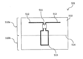
- FIG. 12 is a diagram showing an example of an IC tag that detects opening of an adherend using an IC chip.
- a non-contact communication antenna 512 is formed on a film substrate 510, an IC chip 511 connected thereto is mounted, and further connected to the IC chip 511.
- a loop-shaped disconnection detection wiring 513 is formed and configured on the film substrate 510.
- a perforation 514 is formed on the film substrate 510 to connect two opposing sides, and the perforation 514 enables separation into two regions 510a and 510b. Then, the antenna 512 and the IC chip 511 are provided in one region 510a, and the disconnection detection wiring 513 is formed across the perforation 514.
- the disconnection detection wiring 513 is disconnected accordingly. Then, the fact that the disconnection detection wiring 513 has been disconnected is detected by the IC chip 511, and that fact is transmitted in a contactless manner via the antenna 512. Thereby, it is recognized that the article to which the RFID label 501 is attached has been opened.
- the non-contact communication medium having the above-described disconnection detection wiring by detecting that the disconnection detection wiring has been disconnected, it can be used not only for opening detection of an article but also for quality control of an attached article. This is possible, and the mechanism is disclosed in Patent Document 5.
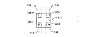
- FIG. 13A is a diagram showing terminals included in the IC chip 511 for explaining the influence on the IC chip 511 in the RFID label 501 shown in FIG.
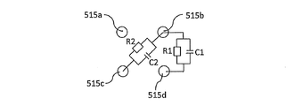
- FIG. 13b is a diagram showing an equivalent circuit between the terminals 515a to 515d shown in FIG. 13a.
- the IC chip 511 of the RFID label 501 shown in FIG. 12 is provided with four terminals 515a to 515d as shown in FIG. 13a. Of the four terminals 515a to 515d, the terminals 515a and 515b are connected to the antenna 512, respectively.
- the terminal 515c is connected to one end of the disconnection detection wiring 513, and the terminal 515d is connected to the other end of the disconnection detection wiring 515.
- the presence or absence of disconnection of the disconnection detection wiring 513 is determined by detecting the change in the resistance value between the two terminals 515c and 515d.
- the RFID label 501 illustrated in FIG. 12 is attached to an article having a metal surface, by separating the terminals 515a and 515b of the IC chip 511 and the antenna 512 from the metal surface, metal for non-contact communication can be provided. The impact can be mitigated. Therefore, the area 510b where the terminals 515a and 515b of the IC chip 511 and the antenna 512 are not provided is attached so as to face the metal surface.
- the terminals 515a and 515b connected to the antenna 512 and the terminals 515c and 515d connected to the disconnection detection wiring 513 are physically independent, they are shown in FIG. 13b in the IC chip 511.
- the present invention has an RFID label that has a state detection wiring and detects the state of an adherend according to the conduction state of the state detection wiring, and the state detection wiring is broken in the state of being attached to a metal.
- An object of the present invention is to provide an RFID label and a state detection method using the RFID label, which can alleviate the influence on non-contact communication.
- the present invention provides An RFID label, which is attached to an adherend having a metal surface and is broken by an external force applied to the adherend, An adhesive layer is laminated on one surface, and a metal attachment area is provided that is directly attached to the metal surface by the adhesive layer, and an easy-to-break line that is broken by the external force is provided in the metal attachment area.
- an IC chip for contact transmission is
- the conduction state of the state detection wiring is detected by the IC chip, and the detection result is transmitted in a contactless manner via the antenna.
- the state detection wiring when attached to an adherend having a metal surface, the state detection wiring straddles an easy-to-break line provided in a metal attachment area directly attached to the metal surface of the adherend.
- the capacitive coupling occurs between the state detection wiring and the metal surface. Even if the state detection wiring is broken by breaking the easy-breakage line from that state, the easy-breakage line is provided in the metal bonding area that is directly bonded to the metal surface of the adherend.
- the sheet base material is configured to be attached to a metal surface through a non-metal material in a region other than the metal attachment region, the RFID label has a metal surface. Even when attached to an adherend, non-contact communication can be performed via the antenna without being significantly affected by metal, but the easy-to-break line breaks when an external force is applied to the adherend. It will be easier.
- the IC chip detects the conduction state of the state detection wiring, and the reading means capable of non-contact communication with the IC chip detects the IC chip.
- the result is transmitted in a non-contact manner via the antenna, and the processing means connected to the reading means judges the state of the adherend based on the detection result transmitted from the IC chip to the reading means in a non-contact manner. The condition of the body will be detected.
- an easy-to-break line that breaks due to an external force applied to the adherend is provided in the metal attachment area that is directly attached to the metal surface of the adherend. Therefore, even if the state detection wiring is broken by an external force applied to the adherend, capacitive coupling is maintained between the side of the state detection wiring connected to the IC chip and the metal surface of the adherend. It becomes a state. Thereby, in the RFID label which has the state detection wiring and detects the state of the adherend according to the conduction state of the state detection wiring, when the state detection wiring is broken in the state of being adhered to the metal In addition, it is possible to mitigate the effect on contactless communication.
- the RFID label in a case where the sheet base material is configured to be attached to a metal surface through a non-metal material in a region other than the metal attachment region, the RFID label has a metal surface. Even if it is attached to an adherend equipped with it, it is possible to perform non-contact communication via the antenna without being greatly affected by the metal, but to easily break the line when an external force is applied to the adherend. It can be easily broken.
- the IC chip detects the conduction state of the state detection wiring, and the IC chip has a reading means capable of non-contact communication with the IC chip.
- the processing means connected to the reading means determines the state of the adherend based on the detection result transmitted in a non-contact manner from the IC chip to the reading means. The state of the adherend can be detected.
- FIG. 1B is a sectional view taken along the line A-A′ shown in FIG. 1A. It is a figure for demonstrating the effect
- FIGS. 1A and 1B are diagrams showing a result of measuring a communication distance when the RFID label is attached to the box as shown in FIGS. 2A and 2B, in comparison with the RFID label shown in FIG. is there. It is the block diagram which looked at 2nd Embodiment of the RFID label of this invention from the surface direction.
- FIG. 4B is a cross-sectional view taken along the line A-A′ shown in FIG. 4A.
- 4B is a cross-sectional view taken along the line B-B′ shown in FIG. 4A.
- 4C is a cross-sectional view taken along the line C-C′ shown in FIG. 4A.
- FIG. 5 is a top view showing an example of an adherend to which the looseness detection label shown in FIGS. 4a to 4d is attached.
- FIG. 5 is a top view showing an example of an adherend to which the looseness detection label shown in FIGS. 4a to 4d is attached.
- FIG. 5B is a side view of the adherend shown in FIG. 5A.
- FIG. 5 is a top view showing an example of a state in which the looseness detection label shown in FIGS. 4a to 4d is attached to the adherend shown in FIGS. 5a and 5b. It is the side view seen from the A direction shown in FIG. 6a. It is the side view seen from the B direction shown in FIG. 6a. An upper surface for explaining the operation when the looseness detection label shown in FIGS. 4a to 4d is adhered across the bolt and the base as shown in FIGS. 6a to 6c when the bolt is loosened. It is a figure. It is the side view seen from the A direction shown in FIG. 7a.
- FIG. 5 is a diagram showing an example of a system for detecting looseness of a bolt with respect to a base using the looseness detection label shown in FIGS. 4a to 4d.
- 9 is a flow chart for explaining a method of detecting looseness of a bolt with respect to a base using the looseness detection label shown in FIGS. 4a to 4d in the system shown in FIG.
- 10b is a back view of the RFID label shown in FIG. 10a.
- FIG. It is a front view which shows other embodiment of the RFID label of this invention.
- FIG. 11b is a back view of the RFID label shown in FIG. 11a. It is a figure which shows an example of the IC tag which detects opening of an adherend using an IC chip. It is a figure which shows the terminal which the IC chip has for explaining the influence on the IC chip in the RFID label shown in FIG.
- FIG. 14 is a diagram showing an equivalent circuit between the terminals shown in FIG. 13a.
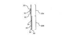
- FIG. 1a is a front view showing a first embodiment of the RFID label of the present invention.
- FIG. 1b is a sectional view taken along the line AA′ shown in FIG. 1a.
- the RFID label in this embodiment is configured by laminating an adhesive layer 50 on a part of the back surface of the film substrate 10 as shown in FIGS. 1a and 1b.
- the film substrate 10 serves as a sheet base material in the present invention.
- the film substrate 10 is made of, for example, a PET film having a thickness of 70 ⁇ m.
- the adhesive layer 50 is laminated on a part of the back surface of the film substrate 10.
- the area where the adhesive layer 50 is laminated serves as a metal adhesion area 10b, and the area where the adhesive layer 50 is not laminated is a non-adhesion area 10a.
- perforations 14 that serve as easy-to-break lines are formed between two opposing edges of the film substrate 10.
- the antenna 12 and the disconnection detection wiring 13 are formed, and the IC chip 11 is mounted.
- the antenna 12 is formed in the non-sticking region 10a of the film substrate 10.
- the antenna 12 is formed by arranging two strip-shaped conductors made of copper foil having a length of 23 mm and a thickness of 18 ⁇ m, for example, in a straight line.
- the antenna 12 constitutes a dipole antenna.
- the disconnection detection wiring 13 serves as the state detection wiring in the present invention.
- the disconnection detection wiring 13 has one end portion in the non-sticking region 10a, extends from there to the sticking region 10b, further extends over the perforations 14 and folds back to the other end portion in the non-sticking region 10a. It has a loop shape. Thereby, the disconnection detection wiring 13 is formed so as to straddle the perforations 14 of the film substrate 10.
- the disconnection detection wiring 14 is formed of, for example, a copper foil having a thickness of 18 ⁇ m.
- the IC chip 11 is provided with two antenna terminals (not shown) and two disconnection detection terminals (not shown) on one surface.
- the IC chip 11 is mounted on the non-sticking region 10a of the film substrate 10 with the surface on which the antenna terminal and the disconnection detection terminal are provided as the mounting surface.
- Each antenna terminal of the IC chip 11 is connected to one end of the antenna 12.
- the disconnection detection terminals of the IC chip 11 are connected to the loop-shaped ends of the disconnection detection wiring 13, respectively.
- the IC chip 11 detects the resistance value of the disconnection detection wiring 13 by causing a current by electric power obtained by the non-contact communication via the antenna 12 to flow in the disconnection detection wiring 13.
- the IC chip 11 detects the conduction state of the disconnection detection wiring 13 based on the resistance value of the disconnection detection wiring 13.
- the IC chip 11 converts the detection result into digital information and transmits it in a contactless manner via the antenna 12.
- Examples of the IC chip 12 include UCODE G2iM+ manufactured by NXP.
- the adhesive layer 50 serves as an adhesive layer in the present invention.
- the adhesive layer 50 is laminated by applying, for example, an adhesive of TL-85 series manufactured by Lintec Co., Ltd. to the adhesion region 10b on the back surface of the film substrate 10.
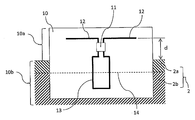
- FIGS. 1a and 1b show a case where the perforation 14 is broken due to a change in the state of the adherend in a state where the RFID label 1 shown in FIGS. 1a and 1b is attached to the adherend made of metal. It is a figure for explaining an operation.
- the RFID label 1 shown in FIGS. 1a and 1b is, for example, as shown in FIG. 2a, a metal box 2 in which a lid 2a made of metal is attached to a main body 2b made of metal so as to be openable and closable. It can be used for open detection.
- the RFID label 1 shown in FIGS. 1a and 1b is used to detect the opening of the metal box 2 as described above, the perforation 14 is formed at the boundary between the lid 2a and the main body 2b, which is the opening part of the box 2.
- the RFID label 1 is attached to the box 2 by the adhesive layer 50 such that the RFID label 1 is overlapped and the attachment area 10b faces the box 2.
- the non-sticking region 10a does not face the box 2 so that the antenna 12 is separated from the box 2. Thereby, the influence of metal on the non-contact communication via the antenna 12 can be mitigated.
- the detected resistance value is the resistance value of the disconnection detection wiring 13 itself, it is determined that the disconnection detection wiring 13 is not disconnected.
- the determination result is converted into digital information by the IC chip 11 as a detection result of the conduction state of the disconnection detection wiring 13, and is transmitted in a contactless manner to the external device via the antenna 12.
- the resistance value detected by the IC chip 11 when the disconnection detection wiring 13 is disconnected is almost infinite as described later. Therefore, in the IC chip 11, as the resistance value for determining that the disconnection detection wiring 13 is not disconnected, a resistance value not exceeding the resistance value of the disconnection detection wiring 13 itself may be used. ..
- the IC chip 11 when the detected resistance value is almost infinite, it is determined that the disconnection detection wiring 13 has a disconnection. The determination result is converted into digital information by the IC chip 11 as a detection result of the conduction state of the disconnection detection wiring 13, and is transmitted in a contactless manner to the external device via the antenna 12.
- the resistance value detected by the IC chip 11 becomes almost infinite. Therefore, in the IC chip 11, the resistance value for determining that the disconnection detection wiring 13 is disconnected is not substantially infinite, and is equal to or larger than a certain threshold value larger than the resistance value of the disconnection detection wiring 13 itself. May be used.
- the conduction state of the disconnection detection wiring 13 is transmitted from the RFID label 1 to the external device, so that in the external device, the box 2 is not opened when the disconnection detection wiring 13 is in the conductive state. If the disconnection detection wiring 13 is in a non-conductive state, it can be determined that the box 2 has been opened.
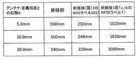
- FIG. 3 shows a result of measuring a communication distance when the RFID label 1 shown in FIGS. 1a and 1b is attached to the box 2 as shown in FIGS. 2a and 2b. It is a figure shown in comparison with.
- the handheld reader/writer of AT880 manufactured by ATiD was used as the external device, and the output of 1.0 W was used for the RFID label 1 with the frequency of 920 MHz band. Contactless communication was performed.
- the RFID label 501 shown in FIG. 12 has an extremely short communication distance of 250 mm. This is because, as described above, in the terminal provided on the IC chip 511, the terminal connected to the antenna 512 and the terminal connected to the disconnection detection wiring 513 are electrically connected via a resistance component or a capacitance component.
- the disconnection detecting wiring 513 When the disconnection detecting wiring 513 is disconnected due to breakage of the perforation 514, the disconnection detecting wire 513, which has been capacitively coupled until now, is not connected. This is because the wiring 513 and the box 2 are not capacitively coupled, and the contactless communication characteristics via the antenna 512 are significantly changed.
- the communication distance is 1020 mm, and the disconnection detection wiring 13 is not disconnected.
- the communication distance does not become extremely short depending on the state. This is because the perforations 14 are provided in the attachment area 10b to be attached to the lid 2a, so that even if the disconnection detection wiring 13 is fractured due to the perforation 14 being fractured, the disconnection detection wiring 13 is also fractured.
- the state in which the capacitive coupling is maintained between the side connected to the IC chip 11 and the box 2 prevents the contactless communication characteristics via the antenna 12 from largely changing, and the contactless metal is used. This is because the influence on communication is mitigated.
- the disconnection detection wiring 13 is disconnected as shown in FIG.
- the communication distance was 560 mm in the non-executed state.
- the RFID label 501 shown in FIG. 12 has an extremely short communication distance of 240 mm.
- the communication distance is 1020 mm, and the communication distance will not be extremely short compared to the state where the disconnection detection wiring 13 is not disconnected.
- the disconnection detection wiring 13 is disconnected as shown in FIG.
- the communication distance was 580 mm in the non-executed state.
- the RFID label 501 shown in FIG. 12 has an extremely short communication distance of 220 mm.
- the communication distance is 1000 mm, and the communication distance will not be extremely short compared to the state where the disconnection detection wiring 13 is not disconnected.
- the disconnection detection wiring 13 is capacitively coupled to the lid 2a and the main body 2b which are made of metal, and the disconnection detection wiring 13 is disconnected even when the disconnection detection wiring 13 is disconnected. Capacitive coupling is maintained between the side of the detection wiring 13 connected to the IC chip 11 and the box 2. As a result, when the disconnection detection wiring 13 is disconnected while the RFID label 1 is attached to the metal box 2 shown in FIGS. 2A and 2B, the non-contact communication due to the change in the capacitive coupling with the box 2. Can be mitigated.
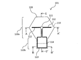
- FIG. 4a is a configuration diagram of a second embodiment of the RFID label of the present invention viewed from the surface direction.
- FIG. 4b is a sectional view taken along the line AA′ shown in FIG. 4a.
- FIG. 4c is a sectional view taken along line BB′ shown in FIG. 4a.
- FIG. 4d is a sectional view taken along line CC′ shown in FIG. 4a.
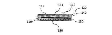
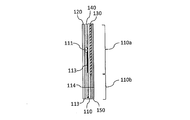
- the RFID label in this embodiment has a protective film 120 laminated on one surface of a film substrate 110 via an adhesive layer 140, and a spacer 130 on the other surface of the film substrate 110.
- the adhesive layer 150 and the adhesive layer 150 are laminated in this order to form the looseness detection label 101 in a label form.
- the film substrate 110 serves as a sheet base material in the present invention.
- the film substrate 110 is made of, for example, a PET film having a thickness of 50 ⁇ m.
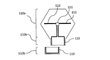
- the film substrate 110 includes a regular hexagonal area 110a formed of a regular hexagonal shape and a protruding area 110b protruding from one end of the regular hexagonal area 110a.
- the two antennas 112 and the state detection wiring 113 are formed on the surface of the film substrate 110 laminated with the protective film 120, and the IC chip 111 is mounted thereon.
- the protruding area 110b becomes the metal attachment area in the present invention.
- Each of the two antennas 112 is formed in a regular hexagonal area 110a on the surface of the film substrate 110 laminated with the protective film 120.
- the two antennas 112 are formed by arranging two strip-shaped conductors made of copper foil having a length of 23 mm and a thickness of 18 ⁇ m, for example, in a straight line.
- the antenna 112 constitutes a dipole antenna.
- the looseness detection wiring 113 serves as the state detection wiring in the present invention.
- the looseness detection wiring 113 is formed on the surface of the film substrate 110 laminated with the protective film 120, for example, with a copper foil having a thickness of 18 ⁇ m.
- the looseness detection wiring 113 has one end portion in the regular hexagonal region 110a, extends from there to the protruding region 110b, is folded back, and has a loop shape having the other end portion in the regular hexagonal region 110a. As a result, the looseness detection wiring 113 is formed so as to straddle the regular hexagonal region 110a and the protruding region 110b.
- the looseness detection wiring 113 has a linear shape along the edge of the film substrate 110 in the protruding area 110b of the attachment area 10a.
- the IC chip 111 is provided with two antenna terminals (not shown) and two looseness detection terminals (not shown) on one surface.
- the IC chip 111 is mounted on the regular hexagonal area 110 a of the film substrate 110, with the surface on which the antenna terminal and the looseness detection terminal are provided as the mounting surface.
- Each antenna terminal of the IC chip 111 is connected to one end of the antenna 112.
- the looseness detection terminals of the IC chip 111 are connected to the loop-shaped ends of the looseness detection wiring 113, respectively.
- the IC chip 111 has a resistance value of the looseness detection wiring 113, which is caused by passing a current due to electric power obtained by non-contact communication via the antenna 112 to the looseness detection wiring 113. To detect.
- the IC chip 111 detects the conduction state of the looseness detection wiring 113 based on the resistance value of the looseness detection wiring 113.
- the IC chip 111 converts the detection result into digital information and transmits it in a contactless manner via the antenna 112. Examples of the IC chip 111 include UCODE G2iM+ manufactured by NXP.
- the protective film 120 is made of, for example, the same material as the film substrate 110.
- the protective film 120 is laminated on the entire surface of the film substrate 110 on which the antenna 112 and the looseness detection wiring 113 are laminated by the adhesive layer 140.
- the spacer 130 is laminated only on the regular hexagonal region 110 a of the surface of the film substrate 110 opposite to the surface on which the antenna 112 and the looseness detection wiring 113 are laminated.
- the spacer 130 is made of a soft non-metallic material such as foamable acrylic resin.
- As the spacer 130 for example, PORON manufactured by Rogers Inoac can be used.
- the adhesive layer 150 serves as an adhesive layer in the present invention.
- the adhesive layer 150 is laminated on the entire surface of the film substrate 110 on which the spacers 130 are laminated, for example, by applying an adhesive of TL-85 series manufactured by Lintec Co., Ltd.
- perforations 114 which are easy-to-break lines that penetrate through the front and back sides, are formed in the protruding regions 110b.
- the looseness detection wiring 113 is formed across the perforations 114. At this time, the perforations 114 are formed so that the cut portion forming the perforations 114 does not disconnect the looseness detection wiring 113.
- FIG. 5a is a top view showing an example of an adherend to which the looseness detection label 101 shown in FIGS. 4a to 4d is attached.
- FIG. 5b is a side view of the adherend shown in FIG. 5a.
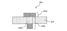
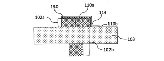
- the looseness detection label 101 shown in FIGS. 4a to 4d is, for example, as shown in FIGS. 5a and 5b, a metal base 103 that is a tightening target component and a metal that is a tightening member that is fastened to the base 103. It is used by being adhered to an adherend composed of the bolt 102 of FIG.
- a bolt 102 including a head portion 102a formed of a regular hexagon and a screw portion 102b extending from one surface of the head portion 102a has a screw portion formed in a screw hole 103a formed in a base 103.
- the screw 102b is screwed, so that the bolt 102 is fastened to the base 103.
- the bolt 102 may be loosened by vibration applied from the outside, and the looseness detection label 101 shown in FIGS. 4a to 4d is used to detect the looseness.
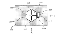
- FIG. 6a is a top view showing an example of a state in which the looseness detection label 101 shown in FIGS. 4a to 4d is attached to the adherend shown in FIGS. 5a and 5b.
- FIG. 6b is a side view seen from the direction A shown in FIG. 6a.
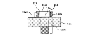
- FIG. 6c is a side view seen from the direction B shown in FIG. 6a. It should be noted that the detailed structure of the looseness detection label 101, such as the laminated structure, is not shown for the sake of clarity.
- the regular hexagonal region 110a of the film substrate 110 faces the upper surface of the head portion 102a of the bolt 102, and regarding the protruding region 110b of the film substrate 110, the region on the regular hexagonal region 110a side through the perforations 114 is the head portion 102a.
- the looseness detection label 101 is attached across the bolt 102 and the base 103 by the adhesive layer 150 so that the area facing the one side surface and the area opposite to the regular hexagonal area 110a via the perforation 114 faces the base 103. Stick it.
- the spacers 130 are laminated only on the regular hexagonal region 110a on the bonding surface of the bolt 102 and the base 103. Therefore, in the film substrate 110, the protruding region 110b is directly attached to the bolt 102 and the base 103 by the adhesive layer 150, and the regular hexagonal region 110a is attached to the bolt 102 via the spacer 130.
- the looseness detection wiring 113 is formed in a loop shape and is in a conductive state. Therefore, as will be described later, in the IC chip 111, it is detected that the looseness detection wiring 113 is in the conductive state. Since the protruding region 110b is directly adhered to the bolt 102 and the base 103 by the adhesive layer 150, capacitive coupling is generated between the looseness detection wiring 113 and the bolt 102 and the base 103.
- FIG. 7a shows that when the looseness detection label 101 shown in FIGS. 4a to 4d is attached across the bolt 102 and the base 103 as shown in FIGS. 6a to 6c, the bolt 102 is loosened.
- FIG. 6 is a top view for explaining the action of the above.
- FIG. 7b is a side view seen from the direction A shown in FIG. 7a.
- FIG. 7C is a diagram showing a state of the looseness detection label 101 when the bolt 102 is loosened. It should be noted that the detailed structure of the looseness detection label 101, such as the laminated structure, is not shown for the sake of clarity.
- the bolt 102 When the looseness detection label 101 shown in FIGS. 4a to 4d is attached over the bolt 102 and the base 103 as shown in FIGS. 6a to 6c, the bolt 102 is moved to the state shown in FIG.
- the film substrate 110 is rotated counterclockwise and loosened with respect to the base 103 as shown in the drawing, the protruding region 110b of the film substrate 110 is a region on the side of the regular hexagonal region 110a through the perforations 114 and one side surface of the head portion 102a. 7b and 7c, since the region facing the base 103 and the region on the opposite side of the regular hexagonal region 110a through the perforations 114 faces the base 103, is attached across the bolt 102 and the base 103. As shown in FIG.
- the perforation 114 is broken, so that the film substrate 110 separates the region on the regular hexagonal region 110a side through the perforation 114 of the regular hexagonal region 110a and the projecting region 110b and the perforation 114 of the projecting region 110b.
- the regular hexagonal region 110a is separated from the regular hexagonal region 110a.
- the looseness detection wiring 113 is broken.
- the spacer 130 is laminated only on the regular hexagonal region 110a of the surface of the film substrate 110 opposite to the surface on which the antenna 112 and the looseness detection wiring 113 are laminated. Since they are not laminated, when the bolt 102 rotates and is displaced with respect to the base 103, the perforations 114 are easily broken. Thereby, the relative displacement between the bolt 102 and the base 103 can be reliably detected.
- the looseness detection wiring 113 is in a non-conductive state is detected in the IC chip 111.
- the region on the regular hexagonal region 110a side is directly attached to the bolt 102 by the adhesive layer 150 via the perforation 114 of the protruding region 110b, the protruding region 110b of the broken looseness detection wiring 113 is formed.
- the capacitive coupling is maintained between the portion formed on the regular hexagonal region 110a side through the perforations 114, that is, the side connected to the IC chip 111 and the bolt 102.
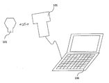
- FIG. 8 is a diagram showing an example of a system for detecting the looseness of the bolt 102 with respect to the base 103 using the looseness detection label 101 shown in FIGS. 4a to 4d.
- non-contact communication is possible with the looseness detection label 101.
- a system having a reader/writer 105 that serves as a reading unit and a management personal computer 106 that serves as a processing unit that is connected to the reader/writer 105 via a wire or wirelessly can be considered. It is also possible to use a handy terminal having a built-in processing unit as well as a reading unit as a reader/writer, in which case a management personal computer becomes unnecessary.
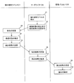
- FIG. 9 is a flow chart for explaining a method of detecting looseness of the bolt 102 with respect to the base 103 using the looseness detection label 101 shown in FIGS. 4a to 4d in the system shown in FIG.
- the reader/writer 105 when the reader/writer 105 is brought close to the looseness detection label 101 and the looseness detection label 101 is detected by the reader/writer 105 (step 1), first, the reader/writer Power is supplied to the looseness detection label 101 from 105. Further, a command to detect the conduction state of the looseness detection wiring 113 and to transmit the detection result is transmitted from the reader/writer 105 to the looseness detection label 101 (step 2). At this time, since the spacer 130 made of non-metal is laminated on the surface of the film substrate 110 on which the antenna 112 is formed and the hexagonal region 110a attached to the bolt 102, the looseness detection label 101 is made of metal. Even when it is attached to the bolt 102, the reader/writer 105 can perform non-contact communication with the looseness detection label 101 without being significantly affected by metal.
- step 3 When the power supplied from the reader/writer 105 is obtained by the looseness detection label 101, and the command transmitted from the reader/writer 105 is received by the IC chip 111 via the antenna 112 of the looseness detection label 101 (step 3). ), current is supplied to the looseness detection wiring 113 by the power supplied from the reader/writer 105.
- the resistance value of the looseness detection wiring 113 is detected using the supplied current. As a result, the conduction state of the looseness detection wiring 113 is detected (step 4).
- the looseness detection label 101 is attached over the bolt 102 and the base 103 and the bolt 102 is not loosened as shown in FIGS. 6a to 6c, the looseness detection wiring 113 is in a conductive state. There is. Therefore, in the IC chip 111, the resistance value of the looseness detection wiring 113 itself is detected.
- the IC chip 111 when the detected resistance value is the resistance value of the looseness detection wiring 113 itself, it is determined that the looseness detection wiring 113 is in a conductive state.
- the determination result is converted into digital information by the IC chip 111 as a detection result of the conduction state of the looseness detection wiring 113, and is transmitted to the reader/writer 105 via the antenna 112 in a non-contact manner (step 5).
- the antenna terminal connected to the antenna 112 of the IC chip 111 and the looseness detection terminal connected to the looseness detection wiring 113 are provided in the IC chip 111 via a resistance component or a capacitance component. It is in an electrically connected state.
- the resistance value detected by the IC chip 111 when the looseness detection wiring 113 is in a non-conductive state is almost infinite, as described later. Therefore, in the IC chip 111, the resistance value for determining that the looseness detection wiring 113 is in the conductive state may be not the resistance value of the looseness detection wiring 113 itself, but may be a certain threshold value or less.
- the looseness detection label 101 is attached across the bolt 102 and the base 103, and as shown in FIGS. 7A to 7C, the looseness detection label 101 is broken at the perforation 114 due to the looseness of the bolt 102.
- the looseness detection wiring 113 is broken, the looseness detection wiring 113 is in a non-conductive state. In this state, even if a current is supplied to the looseness detection wiring 113 by the power supplied from the reader/writer 105, the looseness detection wiring 113 is in a non-conducting state, so that the looseness detection wiring 113 has no current. Does not flow. As a result, the resistance value detected by the IC chip 111 becomes almost infinite.
- the IC chip 111 when the detected resistance value is almost infinite, it is determined that the looseness detection wiring 113 is in the non-conduction state.
- the determination result is converted into digital information by the IC chip 111 as a detection result of the conduction state of the looseness detection wiring 113, and is transmitted to the reader/writer 105 via the antenna 112 in a non-contact manner.
- the protruding region 110b of the broken loosening detection wiring 113 is formed.
- the capacitive coupling is maintained between the portion formed on the regular hexagonal region 110a side through the perforations 114, that is, the side connected to the IC chip 111 and the bolt 102. Therefore, also in this case, the non-contact transmission of the detection result to the reader/writer 105 via the antenna 112 is performed in a state having the influence of this capacitive coupling.
- the resistance value detected by the IC chip 111 is almost infinite when the looseness detection wiring 113 is in the non-conductive state. Therefore, in the IC chip 111, the resistance value for determining that the looseness detection wiring 113 is in the non-conductive state is not substantially infinite, and is equal to or larger than a certain threshold value larger than the resistance value of the looseness detection wiring 113 itself. May be used.
- the conduction state of the looseness detection wiring 113 detected by the looseness detection label 101 is transmitted in a contactless manner via the antenna 112.
- the detection result transmitted in a non-contact manner from the looseness detection label 101 to the reader/writer 105 as described above is received by the reader/writer 105 (step 6)
- the detection result received by the reader/writer 105 is the management personal computer. It is transferred to 106 (step 7).
- the looseness detection label 101 is transmitted to the reader/writer 105 in a non-contact manner by the management personal computer 106, and the management personal computer 106. It is determined whether the bolt 102 is loosened based on the detection result transferred to (step 9). Specifically, in the detection result transferred from the reader/writer 105 to the management personal computer 106, when the looseness detection wiring 113 is in the conductive state, it is determined that the bolt 102 is not loosened, and the looseness detection wiring is obtained. When 113 is in a non-conducting state, it is determined that the bolt 102 is loose.
- the looseness detection wiring 113 when the looseness detection wiring 113 is not broken, the looseness detection wiring 113 is capacitively coupled to the metal bolt 102 or the base 103, and the looseness detection wiring 113 is broken. Also in this case, capacitive coupling is maintained between the side of the looseness detection wiring 113 connected to the IC chip 111 and the bolt 102. As a result, when the looseness detection label 101 is stuck over the metal bolt 102 and the base 103 shown in FIGS. 5a and 5b and the looseness detection wiring 113 is broken, the bolt 102 and the base 103 are broken. The influence on the non-contact communication can be mitigated by the change of the capacitive coupling with.
- the looseness detection label 101 configured in this way can be used, for example, in a bogie of the Shinkansen or the like to detect looseness of a bolt that fixes the bogie.
- the spacer 130 is made of a soft material such as foamable acrylic resin, the looseness detection label 101 is released even when the looseness detection label 101 is blown or dropped due to vibration while the Shinkansen is running. The damage caused by 101 hitting a human body or the like can be reduced.
- FIG. 10a is a front view showing another embodiment of the RFID label of the present invention.
- 10b is a back view of the RFID label shown in FIG. 10a.
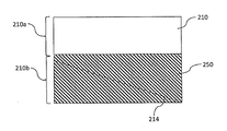
- the RFID label of the present embodiment is different from the RFID label shown in FIGS. 1a and 1b in that perforations 214 are formed between two adjacent edges of the film substrate 210. Is different.
- the perforation 214 is formed in the attachment area 210b that is attached to the metal surface by stacking the adhesive layer 250, and the disconnection detection wiring 213 has the perforation 214. It is formed across. Accordingly, when the attachment area 210b is attached to an adherend made of metal, the disconnection detection is performed in a state where the disconnection detection wiring 213 is not disconnected because the perforation 214 is not broken. The wiring 213 is capacitively coupled to the metal of the adherend. Further, even when the perforation 214 is broken and the disconnection detection wiring 213 is disconnected, capacitive coupling is maintained between the side of the disconnection detection wiring 213 connected to the IC chip 211 and the metal of the adherend. Will be done.
- the disconnection detection wiring 213 is disconnected due to a change in the state of the adherend in a state where the RFID label 201 is attached to the adherend made of a metal, the RFID label 201 is separated from the metal of the adherend.
- the change in capacitive coupling can mitigate the effect on contactless communication.
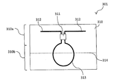
- FIG. 11 a is a front view showing another embodiment of the RFID label of the present invention.
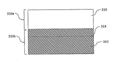
- 11b is a rear view of the RFID label shown in FIG. 11a.
- the RFID label of this embodiment is different from that shown in FIGS. 1a and 1b in that the disconnection detection wiring 313 is circular.
- the adhesive layer 350 is laminated to form the perforations 314 in the attachment area 310b that is attached to the metal surface, and the disconnection detection wiring 213 has the perforations 214. It is formed across. Accordingly, when the attachment area 310b is attached to an adherend made of metal, the disconnection detection is performed in a state where the disconnection detection wiring 313 is not disconnected because the perforation 314 is not broken. The wiring 313 is capacitively coupled to the metal of the adherend. Even when the perforation 314 is broken and the disconnection detection wiring 313 is disconnected, capacitive coupling is maintained between the side of the disconnection detection wiring 313 connected to the IC chip 311 and the metal of the adherend. Will be done.
- the perforations 14, 114, 214, 314 have been described as an example of the easy-to-break line, but the disconnection detection wirings 13, 213, 313 and the looseness detection wiring 113 should be avoided.
- the easily breakable line may be formed by slitting or punching.
- the configuration in which the two antennas 12, 112, 212, 312 are connected to the IC chips 11, 111, 211, 311 has been described as an example, but one loop-shaped antenna is described. May be connected to the IC chip.
Landscapes
- Engineering & Computer Science (AREA)
- Computer Hardware Design (AREA)
- Microelectronics & Electronic Packaging (AREA)
- Physics & Mathematics (AREA)
- General Physics & Mathematics (AREA)
- Theoretical Computer Science (AREA)
- Computer Security & Cryptography (AREA)
- General Engineering & Computer Science (AREA)
- Force Measurement Appropriate To Specific Purposes (AREA)
- Credit Cards Or The Like (AREA)
Abstract
被着体の金属面に直接貼着される貼着領域10bを具備し、貼着領域10b内に外力によって破断するミシン目14が設けられたフィルム基板10と、フィルム基板10の貼着領域10b以外の非貼着領域10aに形成されたアンテナ12と、フィルム基板10にミシン目14を跨いで形成された断線検知用配線13と、フィルム基板10の非貼着領域10aに配置され、アンテナ12及び断線検知用配線13と接続され、断線検知用配線13の導通状態を検出し、その検出結果をアンテナ12を介して非接触送信するICチップ11とを有する。
Description
本発明は、状態検出用配線を有し、状態検出用配線の導通状態に応じて被着体の状態を検出するRFIDラベル及びそれを用いた状態検出方法に関する。
昨今、情報化社会の進展に伴って、商品等に貼付されるラベルやタグに情報を記録し、このラベルやタグを用いて商品等の管理が行われている。このようなラベルやタグを用いた情報管理においては、ラベルやタグに対して非接触状態にて情報の書き込みや読み出しを行うことが可能なICチップが搭載された非接触型ICラベルや非接触型ICタグ等のRFID技術を利用した非接触通信媒体がその優れた利便性から急速な普及が進みつつある。
このような非接触通信媒体においては、金属から構成された物品に取り付けられた場合、アンテナが金属の影響を受け、通信距離が短くなってしまう。そこで、金属の影響を避けるために、グランドを有した立体構造物を利用して非接触通信媒体を金属から構成された物品に取り付けられることが行われている。ところが、その場合、その構造が複雑であり高価なものとなってしまう。
ここで、ラベル基体にRFIDが取り付けられて構成されたRFIDラベルであって、ラベル基体を、折り畳み可能な3つの領域から構成し、3つの領域のうち、RFIDが取り付けられた領域が被着体から離間するように折り畳んで被着体に保持するRFIDラベルが、特許文献1に開示されている。このRFIDラベルを用いることで、被着体が金属から構成されたものである場合に金属による影響を緩和することができる。
また、アンテナ及びICチップが設けられた基材の一部を折り重ねることで、アンテナ及びICチップを物品の金属面から離間させる非接触型データ受送信体が、特許文献2に開示されている。この非接触型データ受送信体を用いることにより、金属による影響を緩和することができる。
また、アンテナの一端を金属面となる放射板と容量結合させるとともに、アンテナの他端を放射板から離間させる無線ICデバイスが、特許文献3に開示されている。この無線ICデバイスを用いることで、金属による影響を緩和することができる。
ところで近年、開封部分を具備する被着体にラベルを貼着しておき、ラベルが剥離されたり破断されたりした場合にそれを検知することで、被着体が開封されたことを検知するための様々な仕組みが考えられている。その中の1つとして、ICチップを用いて被着体の開封を検知する技術が考えられており、例えば、特許文献4に開示されている。
図12は、ICチップを用いて被着体の開封を検知するICタグの一例を示す図である。
本例は図12に示すように、フィルム基板510上に、非接触通信用のアンテナ512が形成されるとともに、これに接続されたICチップ511が搭載され、さらに、ICチップ511に接続されたループ状の断線検知用配線513がフィルム基板510上に形成されて構成されている。
フィルム基板510には、対向する2辺間を結ぶミシン目514が形成されており、このミシン目514によって2つの領域510a,510bに分離可能となっている。そして、アンテナ512及びICチップ511が一方の領域510aに設けられており、断線検知用配線513がミシン目514を跨って形成されている。
上記のように構成されたRFIDラベル501においては、物品の開封部分にミシン目514が対向するように貼着された状態にて物品が開封されると、ミシン目514が破断してフィルム基板510が2つの領域510a,510bに分離し、それに伴って断線検知用配線513が断線する。そして、断線検知用配線513が断線した旨がICチップ511にて検出され、その旨がアンテナ512を介して非接触送信される。これにより、RFIDラベル501が貼着された物品が開封された旨が認識されることになる。
上述した断線検知用配線を有する非接触通信媒体においては、断線検知用配線が断線したことを検出することで、物品の開封検知に限らず、貼着した物品の品質管理にも利用することができ、その仕組みが特許文献5に開示されている。
上述したような断線検知用配線を有するRFIDラベルにおいても、金属面を有する被着体となる物品に貼着して使用する場合、非接触通信への金属による影響を緩和する必要がある。
図13aは、図12に示したRFIDラベル501におけるICチップ511への影響を説明するためのICチップ511が有する端子を示す図である。図13bは、図13aに示した端子515a~515d間の等価回路を示す図である。
図12に示したRFIDラベル501におけるICチップ511には、図13aに示すように4つの端子515a~515dが設けられている。この4つの端子515a~515dのうち、端子515a,515bはアンテナ512にそれぞれ接続されている。また、端子515cは断線検知用配線513の一端に接続され、端子515dは断線検知用配線515の他端に接続されている。ICチップ511においては、2つの端子515c,515d間の抵抗値の変化を検出することで、断線検知用配線513の断線の有無が判断されることになる。
ここで、図12に示したRFIDラベル501を金属面を有する物品に貼着する場合、ICチップ511の端子515a,515b及びアンテナ512を金属面から離間させることで、非接触通信への金属による影響を緩和することができる。そのため、ICチップ511の端子515a,515b及びアンテナ512が設けられていない領域510bが金属面に対向するように貼着することになる。ところが、アンテナ512に接続された端子515a,515bと、断線検知用配線513に接続された端子515c,515dとは、物理的に独立しているものの、ICチップ511内においては、図13bに示すように、抵抗成分R1,R2や容量成分C1,C2を介して電気的に接続された状態となって完全に独立したものとはなっていない。そのため、ミシン目514が破断することで断線検知用配線513が断線した場合に、断線検知用配線513と金属面との容量結合がなくなることでその影響がアンテナ512を介した非接触通信特性に及び、通信距離が短くなってしまうという問題点がある。
本発明は、状態検出用配線を有し、状態検出用配線の導通状態に応じて被着体の状態を検出するRFIDラベルにおいて、金属に貼着された状態にて状態検出用配線が断線した場合に非接触通信に及ぶ影響を緩和することができるRFIDラベル及びそれを用いた状態検出方法を提供することを目的とする。
上記目的を達成するために本発明は、
金属面を具備する被着体に貼着され、前記被着体に加わる外力によって破断するRFIDラベルであって、
一方の面に接着層が積層され、前記接着層によって前記金属面に直接貼着される金属貼着領域を具備し、前記金属貼着領域内に前記外力によって破断する破断容易線が設けられたシート基材と、
前記シート基材の前記金属貼着領域以外の領域に形成されたアンテナと、
前記シート基材に前記破断容易線を跨いで形成された状態検出用配線と、
前記シート基材の前記金属貼着領域以外の領域に配置され、前記アンテナ及び状態検出用配線と接続され、前記状態検出用配線の導通状態を検出し、その検出結果を前記アンテナを介して非接触送信するICチップとを有する。
上記のように構成された本発明においては、ICチップによって状態検知用配線の導通状態が検出され、その検出結果がアンテナを介して非接触送信される。ここで、金属面を具備する被着体に貼着された場合、状態検知用配線が、被着体の金属面に直接貼着される金属貼着領域内に設けられた破断容易線を跨いで形成されていることにより、状態検知用配線と金属面との間で容量結合が生じた状態となっている。その状態から破断容易線が破断することで状態検知用配線が断線した場合であっても、破断容易線が被着体の金属面に直接貼着される金属貼着領域内に設けられていることで、状態検知用配線のICチップに接続された側と被着体の金属面との間にて容量結合が維持された状態となる。それにより、被着体に加わる外力によって破断した場合においても、アンテナを介した非接触通信特性が大きく変化することがなくなり、非接触通信に及ぶ影響が緩和されることになる。
また、このようなRFIDラベルにおいて、シート基材が、金属貼着領域以外の領域が非金属製の材料を介して金属面に貼着される構成とすれば、RFIDラベルが金属面を具備する被着体に貼着された場合でも、金属による影響を大きく受けることなくアンテナを介して非接触通信を行うことができながらも、被着体に外力が加わった場合に破断容易線が破断しやすくなる。
上記のようなRFIDラベルを用いた状態検出方法においては、ICチップが、状態検出用配線の導通状態を検出し、ICチップに対して非接触通信が可能な読取手段が、ICチップに、検出結果をアンテナを介して非接触送信させ、読取手段に接続された処理手段が、ICチップから読取手段に非接触送信された検出結果に基づいて被着体の状態を判断することにより、被着体の状態が検出されることになる。
本発明は、被着体に加わった外力によって破断する破断容易線が、被着体の金属面に直接貼着される金属貼着領域内に設けられている。そのため、被着体に加わった外力によって状態検知用配線が断線した場合でも、状態検知用配線のICチップに接続された側と被着体の金属面との間にて容量結合が維持された状態となる。それにより、状態検出用配線を有し、状態検出用配線の導通状態に応じて被着体の状態を検出するRFIDラベルにおいて、金属に貼着された状態にて状態検出用配線が断線した場合に非接触通信に及ぶ影響を緩和することができる。
また、このようなRFIDラベルにおいて、シート基材が、金属貼着領域以外の領域が非金属製の材料を介して金属面に貼着される構成としたものにおいては、RFIDラベルが金属面を具備する被着体に貼着された場合でも、金属による影響を大きく受けることなくアンテナを介して非接触通信を行うことができながらも、被着体に外力が加わった場合に破断容易線を破断しやすくすることができる。
また、上記のようなRFIDラベルを用いた状態検出方法としては、ICチップが、状態検出用配線の導通状態を検出し、ICチップに対して非接触通信が可能な読取手段が、ICチップに、検出結果をアンテナを介して非接触送信させ、読取手段に接続された処理手段が、ICチップから読取手段に非接触送信された検出結果に基づいて被着体の状態を判断することにより、被着体の状態を検出することができる。
以下に、本発明の実施の形態について図面を参照して説明する。
(第1の実施の形態)
図1aは、本発明のRFIDラベルの第1の実施の形態を示す表面図である。図1bは、図1aに示したA-A’断面図である。
図1aは、本発明のRFIDラベルの第1の実施の形態を示す表面図である。図1bは、図1aに示したA-A’断面図である。
本形態におけるRFIDラベルは図1a及び図1bに示すように、フィルム基板10の裏面の一部に粘着層50が積層されて構成されている。
フィルム基板10は、本願発明におけるシート基材となるものである。フィルム基板10は、例えば、厚さが70μmのPETフィルムから構成されている。フィルム基板10は、裏面の一部に粘着層50が積層されている。フィルム基板10は、粘着層50が積層された領域が金属貼着領域となる貼着領域10bとなり、粘着層50が積層されていない領域が非貼着領域10aとなっている。フィルム基板10の貼着領域10bには、フィルム基板10の対向する2つの端辺間に亘って破断容易線となるミシン目14が形成されている。フィルム基板10の表面には、アンテナ12及び断線検知用配線13が形成されているとともに、ICチップ11が搭載されている。
アンテナ12は、フィルム基板10の非貼着領域10aに形成されている。アンテナ12は、例えば、23mmの長さを具備する厚さが18μmの銅箔による2つの帯状の導体が直線状に並ぶようにして形成されている。アンテナ12は、ダイポールアンテナを構成している。
断線検知用配線13は、本願発明における状態検出用配線となるものである。断線検知用配線13は、非貼着領域10aに一端部を有し、そこから貼着領域10bに延び、さらにミシン目14を跨いで延びて折り返してきて非貼着領域10aに他端部を有するループ状となっている。それにより、断線検知用配線13は、フィルム基板10のミシン目14を跨いで形成されたものとなっている。断線検知用配線14は、例えば、厚さが18μmの銅箔によって形成されている。
ICチップ11は、一方の面に、2つのアンテナ端子(不図示)と、2つの断線検知端子(不図示)とが設けられている。ICチップ11は、これらアンテナ端子及び断線検知端子が設けられた面が搭載面となって、フィルム基板10の非貼着領域10aに搭載されている。ICチップ11のアンテナ端子はそれぞれ、アンテナ12の一端に接続されている。ICチップ11の断線検知端子は、断線検知用配線13のループ状の両端部にそれぞれ接続されている。ICチップ11は、アンテナ12を介した非接触通信によって得た電力による電流を断線検知用配線13に流すことで断線検知用配線13の抵抗値を検出する。ICチップ11は、断線検知用配線13の抵抗値に基づいて断線検知用配線13の導通状態を検出する。ICチップ11は、その検出結果をデジタル情報に変換してアンテナ12を介して非接触送信する。ICチップ12としては、例えば、NXP社のUCODE G2iM+が挙げられる。
粘着層50は、本願発明における接着層となるものである。粘着層50は、フィルム基板10の裏面の貼着領域10bに、例えば、リンテック社製のTL-85シリーズの粘着剤を塗布することで積層されている。
以下に、上記のように構成されたRFIDラベル1の利用方法及びその際の作用について説明する。
図2a及び図2bは、図1a及び図1bに示したRFIDラベル1が金属から構成された被着体に貼着された状態において被着体の状態の変化によってミシン目14が破断した場合の作用を説明するための図である。
図1a及び図1bに示したRFIDラベル1は、例えば、図2aに示すように、金属から構成された本体2bに金属から構成された蓋2aが開閉自在に取り付けられた金属製の箱2の開封検知に利用することができる。このように図1a及び図1bに示したRFIDラベル1を金属製の箱2の開封検知に利用する場合は、箱2の開封部分となる蓋2aと本体2bとの境界部分にミシン目14が重なるとともに、貼着領域10bが箱2に対向するようにRFIDラベル1を粘着層50によって箱2に貼着することになる。その際、非貼着領域10aが箱2に対向しないことでアンテナ12が箱2から離間する。それにより、アンテナ12を介した非接触通信への金属による影響を緩和することができる。
そして、図1a及び図1bに示したRFIDラベル1が図2aに示したように箱2に貼着された状態において箱2が開封されていない場合は、ミシン目14が破断しておらず、それにより、断線検知用配線13が断線していない。その状態において、RFIDラベル1に対して非接触通信を行う外部装置がRFIDラベル1に翳されると、外部装置から供給された電力によって断線検知用配線13に電流が供給されることになる。ICチップ11においては、断線検知用配線13が断線していないことから、断線検知用配線13自体の抵抗値が検出されることになる。
ICチップ11においては、検出された抵抗値が断線検知用配線13自体の抵抗値である場合は、断線検知用配線13に断線が生じていないと判断される。その判断結果は、断線検知用配線13の導通状態の検出結果としてICチップ11にてデジタル情報に変換されてアンテナ12を介して外部装置に非接触送信される。なお、断線検知用配線13が断線している場合にICチップ11にて検出される抵抗値は、後述するようにほぼ無限大となる。そのため、ICチップ11において、断線検知用配線13に断線が生じていないと判断するための抵抗値として、断線検知用配線13自体の抵抗値ではなく、一定の閾値以下のものを用いてもよい。
一方、図1a及び図1bに示したRFIDラベル1が図2aに示したように箱2に貼着された状態において箱2が開封された場合は、図2bに示すように、ミシン目14が破断し、それにより、断線検知用配線13が断線する。その状態においては、RFIDラベル1に対して非接触通信を行う外部装置がRFIDラベル1に翳されることで、外部装置から供給された電力によって断線検知用配線13に電流が供給されても、断線検知用配線13が断線していることから断線検知用配線13には電流が流れない。それにより、ICチップ11において検出される抵抗値は、ほぼ無限大となる。
ICチップ11においては、検出された抵抗値がほぼ無限大である場合は、断線検知用配線13に断線が生じていると判断される。その判断結果は、断線検知用配線13の導通状態の検出結果としてICチップ11にてデジタル情報に変換されてアンテナ12を介して外部装置に非接触送信される。なお、断線検知用配線13が断線している場合にICチップ11にて検出される抵抗値はほぼ無限大となる。そのため、ICチップ11において、断線検知用配線13に断線が生じていると判断するための抵抗値としてほぼ無限大ではなく、断線検知用配線13自体の抵抗値よりも大きな一定の閾値以上のものを用いてもよい。
このようにして断線検知用配線13の導通状態がRFIDラベル1から外部装置に送信されることで、外部装置においては、断線検知用配線13が導通状態である場合は箱2が開封されていないと判断し、断線検知用配線13が非導通状態である場合は箱2が開封されたと判断することができる。
ここで、図1a及び図1bに示したRFIDラベル1において、ミシン目14が貼着領域10bに形成されていることによる作用効果について説明する。
図3は、図1a及び図1bに示したRFIDラベル1が図2a及び図2bに示したように箱2に貼着された場合の通信距離を測定した結果を図12に示したRFIDラベル501と比較して示す図である。なお、RFIDラベル1,501の通信距離の測定においては、外部装置として、ATiD社製AT880のハンディリーダライタを用い、920MHz帯の周波数を用いて、1.0Wの出力でRFIDラベル1に対して非接触通信を行った。
図2a及び図2bに示したRFIDラベル1のアンテナ12と金属端面となる蓋2aとの距離dを5.0mmとした場合の通信距離を測定した結果、図3に示すように、断線検知用配線13が断線していない状態においては通信距離が560mmであった。これに対して、ミシン目14が破断することで断線検知用配線13が断線した状態においては、図12に示したRFIDラベル501では、250mmと通信距離が極端に短くなってしまう。これは、上述したように、ICチップ511に設けられた端子においては、アンテナ512に接続された端子と、断線検知用配線513に接続された端子とが、抵抗成分や容量成分を介して電気的に接続された状態となって完全に独立したものとはなっておらず、ミシン目514が破断することで断線検知用配線513が断線した場合に、これまで容量結合していた断線検知用配線513と箱2とが容量結合していない状態となってしまい、それにより、アンテナ512を介した非接触通信特性が大きく変化してしまうことによるものである。
一方、図1a及び図1bに示したRFIDラベル1においては、断線検知用配線13が断線したとしても、図3に示すように、通信距離が1020mmとなり、断線検知用配線13が断線していない状態に対して通信距離が極端に短くなってしまうことがなくなる。これは、ミシン目14が蓋2aに貼着される貼着領域10bに設けられていることで、ミシン目14が破断することで断線検知用配線13が破断したとしても、断線検知用配線13のICチップ11に接続された側と箱2との間にて容量結合が維持された状態となり、それにより、アンテナ12を介した非接触通信特性が大きく変化することがなくなり、金属による非接触通信への影響が緩和されるためである。
また、図2a及び図2bに示したRFIDラベル1のアンテナ12と金属端面となる蓋2aとの距離dを10.0mmとした場合は、図3に示すように、断線検知用配線13が断線していない状態においては通信距離が560mmであった。これに対して、ミシン目14が破断することで断線検知用配線13が断線した状態においては、図12に示したRFIDラベル501では、240mmと通信距離が極端に短くなってしまうが、図1a及び図1bに示したRFIDラベル1では、通信距離が1020mmとなり、断線検知用配線13が断線していない状態に対して通信距離が極端に短くなってしまうことがなくなる。
また、図2a及び図2bに示したRFIDラベル1のアンテナ12と金属端面となる蓋2aとの距離dを20.0mmとした場合は、図3に示すように、断線検知用配線13が断線していない状態においては通信距離が580mmであった。これに対して、ミシン目14が破断することで断線検知用配線13が断線した状態においては、図12に示したRFIDラベル501では、220mmと通信距離が極端に短くなってしまうが、図1a及び図1bに示したRFIDラベル1では、通信距離が1000mmとなり、断線検知用配線13が断線していない状態に対して通信距離が極端に短くなってしまうことがなくなる。
このように、断線検知用配線13が断線していない状態においては、断線検知用配線13が金属である蓋2aや本体2bと容量結合し、断線検知用配線13が断線した状態においても、断線検知用配線13のICチップ11に接続された側と箱2との間にて容量結合が維持されることになる。これにより、RFIDラベル1が図2a及び図2bに示した金属製の箱2に取り付けられた状態にて断線検知用配線13が断線した場合に、箱2との容量結合の変化によって非接触通信に及ぶ影響を緩和することができる。
(第2の実施の形態)
図4aは、本発明のRFIDラベルの第2の実施の形態を表面方向から見た構成図である。図4bは、図4aに示したA-A’断面図である。図4cは、図4aに示したB-B’断面図である。図4dは、図4aに示したC-C’断面図である。
図4aは、本発明のRFIDラベルの第2の実施の形態を表面方向から見た構成図である。図4bは、図4aに示したA-A’断面図である。図4cは、図4aに示したB-B’断面図である。図4dは、図4aに示したC-C’断面図である。
本形態におけるRFIDラベルは図4a~図4dに示すように、フィルム基板110の一方の面に、粘着層140を介して保護フィルム120が積層され、フィルム基板110の他方の面に、スペーサ130と粘着層150とがこの順で積層されてラベル形態となった緩み検知ラベル101である。
フィルム基板110は、本願発明におけるシート基材となるものである。フィルム基板110は、例えば、厚さが50μmのPETフィルムから構成されている。フィルム基板110は、正六角形から構成された正六角形領域110aと、正六角形領域110aの1つの端辺から突出した突出領域110bとから構成されている。フィルム基板110の保護フィルム120との積層面には、2つのアンテナ112及び状態検出用配線113が形成されているとともに、ICチップ111が搭載されている。なお、突出領域110bが、本願発明における金属貼着領域となる。
2つのアンテナ112はそれぞれ、フィルム基板110の保護フィルム120との積層面のうち正六角形領域110aに形成されている。2つのアンテナ112は、例えば、23mmの長さを具備する厚さが18μmの銅箔による2つの帯状の導体が直線状に並ぶようにして形成されている。アンテナ112は、ダイポールアンテナを構成している。
緩み検知用配線113は、本願発明における状態検出用配線となるものである。緩み検知用配線113は、フィルム基板110の保護フィルム120との積層面に、例えば、厚さが18μmの銅箔によって形成されている。緩み検知用配線113は、正六角形領域110aに一端部を有し、そこから突出領域110bに延びて折り返してきて正六角形領域110aに他端部を有するループ状となっている。これにより、緩み検知用配線113は、正六角形領域110aと突出領域110bとに跨って形成されている。なお、緩み検知用配線113は、貼着領域10aの突出領域110bにおいては、フィルム基板110の端辺に沿った直線状となっている。
ICチップ111は、一方の面に、2つのアンテナ端子(不図示)と、2つの緩み検知端子(不図示)とが設けられている。ICチップ111は、これらアンテナ端子及び緩み検知端子が設けられた面が搭載面となって、フィルム基板110の正六角形領域110aに搭載されている。ICチップ111のアンテナ端子はそれぞれ、アンテナ112の一端に接続されている。ICチップ111の緩み検知端子は、緩み検知用配線113のループ状の両端部にそれぞれ接続されている。ICチップ111は、図1a及び図1bに示したものと同様に、アンテナ112を介した非接触通信によって得た電力による電流を緩み検知用配線113に流すことで緩み検知用配線113の抵抗値を検出する。ICチップ111は、緩み検知用配線113の抵抗値に基づいて緩み検知用配線113の導通状態を検出する。ICチップ111は、その検出結果をデジタル情報に変換してアンテナ112を介して非接触送信する。ICチップ111としては、例えば、NXP社のUCODE G2iM+が挙げられる。
保護フィルム120は、例えば、フィルム基板110と同一の材料から構成されている。保護フィルム120は、フィルム基板110のアンテナ112及び緩み検知用配線113が積層された面の全面に粘着層140によって積層されている。
スペーサ130は、フィルム基板110のアンテナ112及び緩み検知用配線113が積層された面とは反対側の面のうち正六角形領域110aのみに積層されている。スペーサ130は、発泡性アクリル樹脂等のように柔らかい非金属製の材料から構成されている。スペーサ130としては、例えば、ロジャース・イノアック社製のPORONを用いることができる。
粘着層150は、本願発明における接着層となるものである。粘着層150は、フィルム基板110のスペーサ130が積層された面の全面に、例えば、リンテック社製のTL-85シリーズの粘着剤を塗布することで積層されている。
このように積層されたフィルム基板110、保護フィルム120及び粘着層140,150には、突出領域110bに、表裏貫通した破断容易線となるミシン目114が形成されている。緩み検知用配線113は、このミシン目114を跨いで形成されている。この際、ミシン目114は、ミシン目114を構成するカット部が緩み検知用配線113を断線しないように形成されている。
以下に、上記のように構成された緩み検知ラベル101の利用方法及びその際の作用について説明する。
図5aは、図4a~図4dに示した緩み検知ラベル101が貼着される被着体の一例を示す上面図である。図5bは、図5aに示す被着体の側面図である。
図4a~図4dに示した緩み検知ラベル101は、例えば、図5a及び図5bに示すように、締め付け対象部品となる金属製の土台103と、この土台103に締め付けられる締め付け部材となる金属製のボルト102とから構成された被着体に貼着されて使用される。この被着体は、正六角形から構成されたヘッド部102aとヘッド部102aの一方の面から伸びたねじ部102bとから構成されるボルト102が、土台103に形成されたねじ孔103aにねじ部102bがねじ込まれることで、ボルト102が土台103に締め付けられることになる。その際、外部から加わる振動等によってボルト102が緩む可能性があり、その緩みを検知するために図4a~図4dに示した緩み検知ラベル101が利用されることになる。
図6aは、図4a~図4dに示した緩み検知ラベル101が図5a及び図5bに示した被着体に貼着された状態の一例を示す上面図である。図6bは、図6aに示すA方向から見た側面図である。図6cは、図6aに示すB方向から見た側面図である。なお、説明がわかりにくくならないように緩み検知ラベル101の積層構造等の詳細な構成の図示は省略してある。
図4a~図4dに示した緩み検知ラベル101を図5a及び図5bに示した被着体に貼着してボルト102の緩み検知に利用する場合は、図6a~図6cに示すように、フィルム基板110の正六角形領域110aがボルト102のヘッド部102aの上面に対向するとともに、フィルム基板110の突出領域110bについては、ミシン目114を介して正六角形領域110a側の領域がヘッド部102aの1つの側面に対向し、ミシン目114を介して正六角形領域110aとは反対側の領域が土台103に対向するように、緩み検知ラベル101を粘着層150によってボルト102と土台103とに跨って貼着する。この際、フィルム基板110は、ボルト102及び土台103との貼着面のうち正六角形領域110aのみにスペーサ130が積層されている。そのため、フィルム基板110は、突出領域110bが粘着層150によってボルト102及び土台103に直接貼着され、正六角形領域110aがスペーサ130を介してボルト102に貼着された状態となる。
このようにしてボルト102と土台103とに跨って貼着された緩み検知ラベル101においては、緩み検知用配線113が、ループ状に形成されていることで導通状態となっている。そのため、後述するように、ICチップ111において、緩み検知用配線113が導通状態である旨が検出されることになる。突出領域110bが粘着層150によってボルト102及び土台103に直接貼着されていることで、緩み検知用配線113とボルト102及び土台103との間にて容量結合が生じた状態となっている。
図7aは、図4a~図4dに示した緩み検知ラベル101が図6a~図6cに示したようにボルト102と土台103とに跨って貼着された状態においてボルト102に緩みが生じた際の作用を説明するための上面図である。図7bは、図7aに示すA方向から見た側面図である。図7cは、ボルト102に緩みが生じた際の緩み検知ラベル101の状態を示す図である。なお、説明がわかりにくくならないように緩み検知ラベル101の積層構造等の詳細な構成の図示は省略してある。
図4a~図4dに示した緩み検知ラベル101が図6a~図6cに示すようにボルト102と土台103とに跨って貼着された状態において、外部から加わる振動等によってボルト102が図7aに示すように反時計回りに回転して土台103に対して緩みが生じると、フィルム基板110の突出領域110bが、ミシン目114を介して正六角形領域110a側の領域がヘッド部102aの1つの側面に対向し、ミシン目114を介して正六角形領域110aとは反対側の領域が土台103に対向するように、ボルト102と土台103とに跨って貼着されているため、図7b及び図7cに示すようにミシン目114が破断することで、フィルム基板110が、正六角形領域110a及び突出領域110bのミシン目114を介して正六角形領域110a側の領域と、突出領域110bのミシン目114を介して正六角形領域110aとは反対側の領域とに分離する。それにより、緩み検知用配線113が断線することになる。その際、スペーサ130が、フィルム基板110のアンテナ112及び緩み検知用配線113が積層された面とは反対側の面のうち正六角形領域110aのみに積層されていることで、突出領域110bには積層されていないため、ボルト102が回転して土台103に対して変位した場合に、ミシン目114が破断しやすくなっている。それにより、ボルト102と土台103との相対変位を確実に検知することができる。
それにより、後述するように、ICチップ111において、緩み検知用配線113が非導通状態である旨が検出されることになる。その際、突出領域110bのミシン目114を介して正六角形領域110a側の領域が粘着層150によってボルト102に直接貼着されていることで、断線した緩み検知用配線113のうち、突出領域110bのミシン目114を介して正六角形領域110a側の領域に形成された部分、すなわち、ICチップ111に接続された側とボルト102との間にて容量結合が維持された状態となっている。
以下に、上述した作用を利用して土台103に対するボルト102の緩みを検知する具体的な方法について説明する。
図8は、図4a~図4dに示した緩み検知ラベル101を用いて土台103に対するボルト102の緩みを検知するためのシステムの一例を示す図である。
図4a~図4dに示した緩み検知ラベル101を用いて土台103に対するボルト102の緩みを検知するためのシステムとしては、図8に示すように、緩み検知ラベル101に対して非接触通信が可能な読取手段となるリーダライタ105と、リーダライタ105と有線または無線を介して接続された処理手段となる管理用パソコン106とを有するシステムが考えられる。なお、読取手段のみならず処理手段が内蔵されたハンディターミナルをリーダライタとして用いることも考えられ、その場合、管理用パソコンが不要となる。
図9は、図8に示したシステムにおいて図4a~図4dに示した緩み検知ラベル101を用いて土台103に対するボルト102の緩みを検知する方法を説明するためのフローチャートである。
図4a~図4dに示した緩み検知ラベル101においては、リーダライタ105が緩み検知ラベル101に近接され、リーダライタ105にて緩み検知ラベル101が検出されると(ステップ1)、まず、リーダライタ105から、緩み検知ラベル101に電力が供給される。また、緩み検知用配線113の導通状態の検出及びその検出結果の送信をする旨の命令がリーダライタ105から緩み検知ラベル101に対して送信される(ステップ2)。この際、フィルム基板110のアンテナ112が形成された正六角形領域110aのボルト102との貼着面に、非金属から構成されたスペーサ130が積層されているため、緩み検知ラベル101が金属から構成されたボルト102に貼着された場合でも、金属による影響を大きく受けることなくリーダライタ105にて緩み検知ラベル101との間にて非接触通信を行うことができる。
リーダライタ105から供給された電力が緩み検知ラベル101にて得られるとともに、リーダライタ105から送信された命令が緩み検知ラベル101のアンテナ112を介してICチップ111にて受信されると(ステップ3)、リーダライタ105から供給された電力によって緩み検知用配線113に電流が供給される。
ICチップ111においては、供給された電流を用いて緩み検知用配線113の抵抗値が検出される。これにより、緩み検知用配線113の導通状態が検出されることになる(ステップ4)。ここで、緩み検知ラベル101がボルト102及び土台103に跨って貼着され、図6a~図6cに示したようにボルト102が緩んでいない場合は、緩み検知用配線113が導通状態となっている。そのため、ICチップ111においては緩み検知用配線113自体の抵抗値が検出されることになる。またこの際、突出領域110bが粘着層150によってボルト102及び土台103に直接貼着されていることで、緩み検知用配線113とボルト102及び土台103との間にて容量結合が生じた状態となっている。
ICチップ111においては、検出された抵抗値が緩み検知用配線113自体の抵抗値である場合は、緩み検知用配線113が導通状態にあると判断される。その判断結果は、緩み検知用配線113の導通状態の検出結果としてICチップ111にてデジタル情報に変換されてアンテナ112を介してリーダライタ105に非接触送信される(ステップ5)。この際、上述したように、ICチップ111のアンテナ112に接続されたアンテナ端子と、緩み検知用配線113に接続された緩み検知端子とは、ICチップ111内において抵抗成分や容量成分を介して電気的に接続された状態となっている。それにより、緩み検知用配線113とボルト102及び土台103との間にて容量結合が生じた状態となっている。そのため、アンテナ112を介したリーダライタ105への検出結果の非接触送信は、この容量結合の影響を有する状態で行われることになる。なお、緩み検知用配線113が非導通状態となっている場合にICチップ111にて検出される抵抗値は、後述するようにほぼ無限大となる。そのため、ICチップ111において、緩み検知用配線113が導通状態にあると判断するための抵抗値として、緩み検知用配線113自体の抵抗値ではなく、一定の閾値以下のものを用いてもよい。
一方、緩み検知ラベル101がボルト102及び土台103に跨って貼着され、図7a~図7cに示したようにボルト102に緩みが生じることにより緩み検知ラベル101がミシン目114にて破断して緩み検知用配線113が断線している場合は、緩み検知用配線113が非導通状態となっている。その状態においては、リーダライタ105から供給された電力によって緩み検知用配線113に電流が供給されても、緩み検知用配線113が非導通状態となっていることから緩み検知用配線113には電流が流れない。それにより、ICチップ111において検出される抵抗値は、ほぼ無限大となる。
ICチップ111においては、検出された抵抗値がほぼ無限大である場合は、緩み検知用配線113が非導通状態になっている判断される。その判断結果は、緩み検知用配線113の導通状態の検出結果としてICチップ111にてデジタル情報に変換されてアンテナ112を介してリーダライタ105に非接触送信される。この際、突出領域110bのミシン目114を介して正六角形領域110a側の領域が粘着層150によってボルト102に直接貼着されていることで、断線した緩み検知用配線113のうち、突出領域110bのミシン目114を介して正六角形領域110a側の領域に形成された部分、すなわち、ICチップ111に接続された側とボルト102との間にて容量結合が維持された状態となっている。そのため、この場合においても、アンテナ112を介したリーダライタ105への検出結果の非接触送信は、この容量結合の影響を有する状態で行われることになる。なお、緩み検知用配線113が非導通状態である場合にICチップ111にて検出される抵抗値はほぼ無限大となる。そのため、ICチップ111において、緩み検知用配線113が非導通状態であると判断するための抵抗値としてほぼ無限大ではなく、緩み検知用配線113自体の抵抗値よりも大きな一定の閾値以上のものを用いてもよい。
このように、リーダライタ105においては、緩み検知ラベル101にて検出された緩み検知用配線113の導通状態を、アンテナ112を介して非接触送信させることになる。
上記のようにして緩み検知ラベル101からリーダライタ105に非接触送信された検出結果がリーダライタ105にて受信されると(ステップ6)、リーダライタ105にて受信された検出結果は管理用パソコン106に転送される(ステップ7)。
リーダライタ5から転送されてきた検出結果が管理用パソコン6にて受信されると(ステップ8)、管理用パソコン106において、緩み検知ラベル101からリーダライタ105に非接触送信され、管理用パソコン106に転送されてきた検出結果に基づいて、ボルト102に緩みが生じているかが判断されることになる(ステップ9)。具体的には、リーダライタ105から管理用パソコン106に転送されてきた検出結果において、緩み検知用配線113が導通状態である場合はボルト102に緩みが生じていないと判断され、緩み検知用配線113が非導通状態である場合はボルト102に緩みが生じていると判断されることになる。
このように本形態においては、緩み検知用配線113が断線していない状態においては、緩み検知用配線113が金属であるボルト102や土台103と容量結合し、緩み検知用配線113が断線した状態においても、緩み検知用配線113のICチップ111に接続された側とボルト102との間にて容量結合が維持されることになる。これにより、緩み検知ラベル101が図5a及び図5bに示した金属製のボルト102と土台103とに跨って貼着された状態で緩み検知用配線113が断線した場合に、ボルト102及び土台103との容量結合の変化によって非接触通信に及ぶ影響を緩和することができる。
このように構成された緩み検知ラベル101は、例えば、新幹線の台車等において、台車を固定するボルトの緩み検知に用いることができる。その場合、スペーサ130が発泡性アクリル樹脂等のように柔らかい材料から構成されていれば、新幹線が走行中に緩み検知ラベル101が風で飛ばされたり振動で脱落したりした場合でも、緩み検知ラベル101が人体等に当たることによる被害を小さくすることができる。
(他の実施の形態)
図10aは、本発明のRFIDラベルの他の実施の形態を示す表面図である。図10bは、図10aに示すRFIDラベルの裏面図である。
図10aは、本発明のRFIDラベルの他の実施の形態を示す表面図である。図10bは、図10aに示すRFIDラベルの裏面図である。
本形態のRFIDラベルは図10a及び図10bに示すように、図1a及び図1bに示したものに対して、ミシン目214が、フィルム基板210の隣接する2つの端辺間に亘って形成されている点が異なるものである。
上記のように構成されたRFIDラベル201においては、粘着層250が積層されることで金属面に貼着される貼着領域210bにミシン目214が形成され、断線検知用配線213がミシン目214を跨って形成されている。これにより、貼着領域210bが金属から構成された被着体に貼着された場合に、ミシン目214が破断していないことで断線検知用配線213が断線していない状態においては、断線検知用配線213が被着体の金属と容量結合している。また、ミシン目214が破断して断線検知用配線213が断線した状態においても、断線検知用配線213のICチップ211に接続された側と被着体の金属との間にて容量結合が維持されることになる。これにより、RFIDラベル201が金属から構成された被着体に貼着された状態にて、被着体の状態の変化によって断線検知用配線213が断線した場合に、被着体の金属との容量結合の変化によって非接触通信に及ぶ影響を緩和することができる。
図11aは、本発明のRFIDラベルの他の実施の形態を示す表面図である。図11bは、図11aに示すRFIDラベルの裏面図である。
本形態のRFIDラベルは図11a及び図11bに示すように、図1a及び図1bに示したものに対して、断線検知用配線313が円型となっている点が異なるものである。
上記のように構成されたRFIDラベル301においては、粘着層350が積層されることで金属面に貼着される貼着領域310bにミシン目314が形成され、断線検知用配線213がミシン目214を跨って形成されている。これにより、貼着領域310bが金属から構成された被着体に貼着された場合に、ミシン目314が破断していないことで断線検知用配線313が断線していない状態においては、断線検知用配線313が被着体の金属と容量結合している。また、ミシン目314が破断して断線検知用配線313が断線した状態においても、断線検知用配線313のICチップ311に接続された側と被着体の金属との間にて容量結合が維持されることになる。これにより、RFIDラベル301が金属から構成された被着体に貼着された状態にて、被着体の状態の変化によって断線検知用配線313が断線した場合に、被着体の金属との容量結合の変化によって非接触通信に及ぶ影響を緩和することができる。
なお、上述した実施の形態においては、破断容易線としてミシン目14,114,214,314を例に挙げて説明したが、断線検知用配線13,213,313や緩み検知用配線113を避けるようにスリット加工や抜き加工を施すことで破断容易線を構成してもよい。
また、上述した実施の形態においては、ICチップ11,111,211,311に2つのアンテナ12,112,212,312が接続された構成を例に挙げて説明したが、ループ状の1つのアンテナがICチップに接続された構成であってもよい。
1,201,301 RFIDラベル
2 箱
2a 蓋
2b 本体
10,110,210,310 フィルム基板
10a,210a,310b 非貼着領域
10b,210b,310b 貼着領域
11,111,211,311 ICチップ
12,112,212,312 アンテナ
13,213,313 断線検知用配線
14,114,214,314 ミシン目
50,140,150,250,350 粘着層
101 緩み検知ラベル
105 リーダライタ
106 管理用パソコン
110a 正六角形領域
110b 突出領域
113 緩み検知用配線
120 保護フィルム
130 スペーサ
102 ボルト
102a ヘッド部
102b ねじ部
103 土台
103a ねじ孔
Claims (3)
- 金属面を具備する被着体に貼着され、前記被着体に加わる外力によって破断するRFIDラベルであって、
一方の面に接着層が積層され、前記接着層によって前記金属面に直接貼着される金属貼着領域を具備し、前記金属貼着領域内に前記外力によって破断する破断容易線が設けられたシート基材と、
前記シート基材の前記金属貼着領域以外の領域に形成されたアンテナと、
前記シート基材に前記破断容易線を跨いで形成された状態検出用配線と、
前記シート基材の前記金属貼着領域以外の領域に配置され、前記アンテナ及び状態検出用配線と接続され、前記状態検出用配線の導通状態を検出し、その検出結果を前記アンテナを介して非接触送信するICチップとを有する、RFIDラベル。 - 請求項1に記載のRFIDラベルにおいて、
前記シート基材は、前記金属貼着領域以外の領域が非金属製の材料を介して前記金属面に貼着される、RFIDラベル。 - 請求項1または請求項2に記載のRFIDラベルを用いた状態検出方法であって、
前記ICチップが、前記状態検出用配線の導通状態を検出するステップと、
前記ICチップに対して非接触通信が可能な読取手段が、前記ICチップに、前記検出結果を前記アンテナを介して非接触送信させるステップと、
前記読取手段に接続された処理手段が、前記ICチップから前記読取手段に非接触送信された検出結果に基づいて前記被着体の状態を判断するステップとを有する、状態検出方法。
Applications Claiming Priority (2)
| Application Number | Priority Date | Filing Date | Title |
|---|---|---|---|
| JP2018239470A JP2020101979A (ja) | 2018-12-21 | 2018-12-21 | Rfidラベル及びそれを用いた状態検出方法 |
| JP2018-239470 | 2018-12-21 |
Publications (1)
| Publication Number | Publication Date |
|---|---|
| WO2020129889A1 true WO2020129889A1 (ja) | 2020-06-25 |
Family
ID=71101302
Family Applications (1)
| Application Number | Title | Priority Date | Filing Date |
|---|---|---|---|
| PCT/JP2019/049145 Ceased WO2020129889A1 (ja) | 2018-12-21 | 2019-12-16 | Rfidラベル及びそれを用いた状態検出方法 |
Country Status (2)
| Country | Link |
|---|---|
| JP (1) | JP2020101979A (ja) |
| WO (1) | WO2020129889A1 (ja) |
Families Citing this family (1)
| Publication number | Priority date | Publication date | Assignee | Title |
|---|---|---|---|---|
| JP7767744B2 (ja) * | 2021-06-17 | 2025-11-12 | Toppanホールディングス株式会社 | 包材 |
Citations (1)
| Publication number | Priority date | Publication date | Assignee | Title |
|---|---|---|---|---|
| JP2018529119A (ja) * | 2015-09-08 | 2018-10-04 | 凸版印刷株式会社 | Icタグ付きシール及びその取り付け方法 |
Family Cites Families (1)
| Publication number | Priority date | Publication date | Assignee | Title |
|---|---|---|---|---|
| JP6862243B2 (ja) * | 2017-03-30 | 2021-04-21 | キヤノン株式会社 | 媒体 |
-
2018
- 2018-12-21 JP JP2018239470A patent/JP2020101979A/ja active Pending
-
2019
- 2019-12-16 WO PCT/JP2019/049145 patent/WO2020129889A1/ja not_active Ceased
Patent Citations (1)
| Publication number | Priority date | Publication date | Assignee | Title |
|---|---|---|---|---|
| JP2018529119A (ja) * | 2015-09-08 | 2018-10-04 | 凸版印刷株式会社 | Icタグ付きシール及びその取り付け方法 |
Also Published As
| Publication number | Publication date |
|---|---|
| JP2020101979A (ja) | 2020-07-02 |
Similar Documents
| Publication | Publication Date | Title |
|---|---|---|
| US9617038B2 (en) | Container including an inlet having an IC chip and an antenna for monitoring tamper events of the container | |
| JP6973379B2 (ja) | Icタグ付きシール、その取り付け方法、及び蓋付き容器 | |
| US8179264B2 (en) | Radio frequency identification tag device for metallic products | |
| CN105701536B (zh) | 非接触ic标签以及标牌 | |
| JP7084269B2 (ja) | 非接触通信媒体 | |
| CN101874252B (zh) | 抗撕裂电路 | |
| US20120074229A1 (en) | Radio frequency ic device and method of manufacturing the same | |
| WO2020129890A1 (ja) | 緩み検知ラベル及びこれを用いた緩み検知方法 | |
| JP2011059969A (ja) | Rfidタグ | |
| JP2020101979A (ja) | Rfidラベル及びそれを用いた状態検出方法 | |
| US20140224882A1 (en) | Flexible Smart Card Transponder | |
| JP2012230469A (ja) | 非接触式icラベル | |
| JP2013242731A (ja) | 無線タグ | |
| JP7407044B2 (ja) | 亀裂検知ラベルセット | |
| JP7138555B2 (ja) | Rfidラベル、緩み検知構造及び緩み検知方法 | |
| CN117460675A (zh) | 开封检测片材、包装件 | |
| JP7173900B2 (ja) | 亀裂検知用ラベル | |
| JP7033898B2 (ja) | ライナーレスラベル | |
| CN104933462B (zh) | 车灯易碎标签 | |
| JP7442360B2 (ja) | 検知部材セット | |
| WO2020189474A1 (ja) | 緩み検知ラベル及び緩み検知構造 | |
| JP2020161124A (ja) | 緩み検知ラベル及び緩み検知構造 | |
| CN105989396A (zh) | 电子标签 | |
| JP2014160174A (ja) | Icタグラベル | |
| JP7407043B2 (ja) | 亀裂検知ラベルセット |
Legal Events
| Date | Code | Title | Description |
|---|---|---|---|
| 121 | Ep: the epo has been informed by wipo that ep was designated in this application |
Ref document number: 19898923 Country of ref document: EP Kind code of ref document: A1 |
|
| NENP | Non-entry into the national phase |
Ref country code: DE |
|
| 122 | Ep: pct application non-entry in european phase |
Ref document number: 19898923 Country of ref document: EP Kind code of ref document: A1 |