WO2020121596A1 - Piezoelectric transducer - Google Patents
Piezoelectric transducer Download PDFInfo
- Publication number
- WO2020121596A1 WO2020121596A1 PCT/JP2019/032100 JP2019032100W WO2020121596A1 WO 2020121596 A1 WO2020121596 A1 WO 2020121596A1 JP 2019032100 W JP2019032100 W JP 2019032100W WO 2020121596 A1 WO2020121596 A1 WO 2020121596A1
- Authority
- WO
- WIPO (PCT)
- Prior art keywords
- piezoelectric transducer
- piezoelectric
- electrode layer
- present
- layer
- Prior art date
Links
- 239000000463 material Substances 0.000 claims description 19
- 238000004873 anchoring Methods 0.000 abstract 3
- 238000000034 method Methods 0.000 description 53
- 238000004519 manufacturing process Methods 0.000 description 38
- 238000010586 diagram Methods 0.000 description 22
- 238000005530 etching Methods 0.000 description 13
- 239000000758 substrate Substances 0.000 description 9
- 230000000052 comparative effect Effects 0.000 description 6
- 238000000708 deep reactive-ion etching Methods 0.000 description 6
- 238000007747 plating Methods 0.000 description 6
- 238000001039 wet etching Methods 0.000 description 5
- 238000005229 chemical vapour deposition Methods 0.000 description 3
- 239000007769 metal material Substances 0.000 description 3
- 238000012986 modification Methods 0.000 description 3
- 230000004048 modification Effects 0.000 description 3
- 238000005240 physical vapour deposition Methods 0.000 description 3
- 239000004020 conductor Substances 0.000 description 2
- 229910052451 lead zirconate titanate Inorganic materials 0.000 description 2
- 238000000059 patterning Methods 0.000 description 2
- WSMQKESQZFQMFW-UHFFFAOYSA-N 5-methyl-pyrazole-3-carboxylic acid Chemical compound CC1=CC(C(O)=O)=NN1 WSMQKESQZFQMFW-UHFFFAOYSA-N 0.000 description 1
- PIGFYZPCRLYGLF-UHFFFAOYSA-N Aluminum nitride Chemical compound [Al]#N PIGFYZPCRLYGLF-UHFFFAOYSA-N 0.000 description 1
- 229910013641 LiNbO 3 Inorganic materials 0.000 description 1
- 229910004298 SiO 2 Inorganic materials 0.000 description 1
- 230000015572 biosynthetic process Effects 0.000 description 1
- 239000000919 ceramic Substances 0.000 description 1
- 239000000470 constituent Substances 0.000 description 1
- 239000013078 crystal Substances 0.000 description 1
- 238000010292 electrical insulation Methods 0.000 description 1
- 239000012212 insulator Substances 0.000 description 1
- HFGPZNIAWCZYJU-UHFFFAOYSA-N lead zirconate titanate Chemical compound [O-2].[O-2].[O-2].[O-2].[O-2].[Ti+4].[Zr+4].[Pb+2] HFGPZNIAWCZYJU-UHFFFAOYSA-N 0.000 description 1
- GQYHUHYESMUTHG-UHFFFAOYSA-N lithium niobate Chemical compound [Li+].[O-][Nb](=O)=O GQYHUHYESMUTHG-UHFFFAOYSA-N 0.000 description 1
- 229910052755 nonmetal Inorganic materials 0.000 description 1
- 230000000149 penetrating effect Effects 0.000 description 1
- 230000035515 penetration Effects 0.000 description 1
- 238000004080 punching Methods 0.000 description 1
- 229910052710 silicon Inorganic materials 0.000 description 1
- 239000010703 silicon Substances 0.000 description 1
Images


Classifications
-
- H—ELECTRICITY
- H10—SEMICONDUCTOR DEVICES; ELECTRIC SOLID-STATE DEVICES NOT OTHERWISE PROVIDED FOR
- H10N—ELECTRIC SOLID-STATE DEVICES NOT OTHERWISE PROVIDED FOR
- H10N30/00—Piezoelectric or electrostrictive devices
- H10N30/20—Piezoelectric or electrostrictive devices with electrical input and mechanical output, e.g. functioning as actuators or vibrators
- H10N30/204—Piezoelectric or electrostrictive devices with electrical input and mechanical output, e.g. functioning as actuators or vibrators using bending displacement, e.g. unimorph, bimorph or multimorph cantilever or membrane benders
- H10N30/2041—Beam type
- H10N30/2042—Cantilevers, i.e. having one fixed end
-
- B—PERFORMING OPERATIONS; TRANSPORTING
- B81—MICROSTRUCTURAL TECHNOLOGY
- B81B—MICROSTRUCTURAL DEVICES OR SYSTEMS, e.g. MICROMECHANICAL DEVICES
- B81B3/00—Devices comprising flexible or deformable elements, e.g. comprising elastic tongues or membranes
-
- H—ELECTRICITY
- H04—ELECTRIC COMMUNICATION TECHNIQUE
- H04R—LOUDSPEAKERS, MICROPHONES, GRAMOPHONE PICK-UPS OR LIKE ACOUSTIC ELECTROMECHANICAL TRANSDUCERS; DEAF-AID SETS; PUBLIC ADDRESS SYSTEMS
- H04R17/00—Piezoelectric transducers; Electrostrictive transducers
-
- H—ELECTRICITY
- H10—SEMICONDUCTOR DEVICES; ELECTRIC SOLID-STATE DEVICES NOT OTHERWISE PROVIDED FOR
- H10N—ELECTRIC SOLID-STATE DEVICES NOT OTHERWISE PROVIDED FOR
- H10N30/00—Piezoelectric or electrostrictive devices
- H10N30/80—Constructional details
- H10N30/85—Piezoelectric or electrostrictive active materials
- H10N30/853—Ceramic compositions
- H10N30/8542—Alkali metal based oxides, e.g. lithium, sodium or potassium niobates
-
- H—ELECTRICITY
- H10—SEMICONDUCTOR DEVICES; ELECTRIC SOLID-STATE DEVICES NOT OTHERWISE PROVIDED FOR
- H10N—ELECTRIC SOLID-STATE DEVICES NOT OTHERWISE PROVIDED FOR
- H10N30/00—Piezoelectric or electrostrictive devices
- H10N30/80—Constructional details
- H10N30/85—Piezoelectric or electrostrictive active materials
- H10N30/853—Ceramic compositions
- H10N30/8548—Lead based oxides
- H10N30/8554—Lead zirconium titanate based
-
- H—ELECTRICITY
- H10—SEMICONDUCTOR DEVICES; ELECTRIC SOLID-STATE DEVICES NOT OTHERWISE PROVIDED FOR
- H10N—ELECTRIC SOLID-STATE DEVICES NOT OTHERWISE PROVIDED FOR
- H10N30/00—Piezoelectric or electrostrictive devices
- H10N30/80—Constructional details
- H10N30/87—Electrodes or interconnections, e.g. leads or terminals
- H10N30/877—Conductive materials
Definitions
- the present invention relates to a piezoelectric transducer.
- Patent Document 1 Japanese Patent Publication No. 2014-515214
- the piezoelectric transducer described in Patent Document 1 includes a substrate and a plurality of cantilevers. Each of the plurality of cantilevers is adjacent to each other and is tapered. Each of the plurality of cantilever beams defines a beam base end portion, a beam tip end portion, and a beam main body portion. The beam main body portion is arranged between the beam base end portion and the beam tip end portion. Each of the plurality of cantilever beams is arranged so that the tip end portion of the beam extends toward a common virtual point. Each of the plurality of cantilevers is coupled to the substrate along the beam base end portion, but is not coupled to the substrate along the beam body portion.
- a pattern such as a piezoelectric layer is formed on the surface side of the substrate. Also, a recess is provided in the substrate by performing processing such as deep reactive ion etching (Deep RIE: Deep Reactive Ion Etching) or wet etching from the back surface side of the substrate.
- processing such as deep reactive ion etching (Deep RIE: Deep Reactive Ion Etching) or wet etching from the back surface side of the substrate.
- the present invention has been made in view of the above problems, and provides a piezoelectric transducer in which the input/output characteristics are improved by making the lengths of the movable portions of the plurality of beam portions uniform.
- the purpose is to
- the piezoelectric transducer includes a base portion, a plurality of beam portions, and at least one fixing portion.
- Each of the plurality of beam portions has an end portion supported by the base portion, and extends at a position above the base portion in a direction away from the base portion.
- Each of the plurality of beam portions includes a plurality of layers.
- Each of the plurality of beam portions has a piezoelectric layer, an upper electrode layer disposed above the piezoelectric layer, and a lower electrode disposed so as to face at least a part of the upper electrode layer with the piezoelectric layer sandwiched therebetween.
- the fixing portion is arranged on the beam portion so as to sandwich each end of the plurality of beam portions with the base portion.
- the fixing portion is positioned so as to overlap at least a part of the base portion in the vertical direction, and extends so as to project from the base portion in the extending direction of the beam portion.
- the input/output characteristics of the piezoelectric transducer can be improved by making the lengths of the movable portions of the plurality of beam portions uniform.
- FIG. 3 is a plan view showing the configuration of the piezoelectric transducer according to the first embodiment of the present invention.
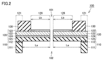
- FIG. 2 is a cross-sectional view of the piezoelectric transducer shown in FIG. 1 as seen in the direction of arrows II-II.
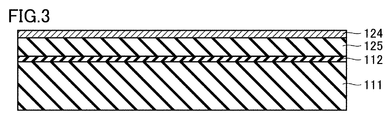
- FIG. 6 is a cross-sectional view showing a state in which a lower electrode layer is provided on the upper surface of the active layer in the method for manufacturing the piezoelectric transducer according to the first embodiment of the present invention.
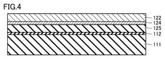
- FIG. 6 is a cross-sectional view showing a state in which a piezoelectric layer is provided on the upper surface of the lower electrode layer in the method of manufacturing the piezoelectric transducer according to the first embodiment of the present invention.
- FIG. 1 is a cross-sectional view showing the configuration of the piezoelectric transducer according to the first embodiment of the present invention.
- FIG. 2 is a cross-sectional view of the piezoelectric transducer shown in FIG. 1 as seen in the
- FIG. 3 is a cross-sectional view showing a state in which an upper electrode layer is provided on the upper surface of the piezoelectric layer in the method of manufacturing the piezoelectric transducer according to the first embodiment of the present invention.
- FIG. 5 is a diagram showing a state in which the upper electrode layer is patterned in the method of manufacturing the piezoelectric transducer according to the first embodiment of the present invention.
- FIG. 5 is a diagram showing a state in which the piezoelectric layer is patterned in the method of manufacturing the piezoelectric transducer according to the first embodiment of the present invention.
- FIG. 5 is a diagram showing a state in which the lower electrode layer is patterned in the method of manufacturing the piezoelectric transducer according to the first embodiment of the present invention.
- FIG. 5 is a diagram showing a state in which the active layer is patterned in the method of manufacturing the piezoelectric transducer according to the first embodiment of the present invention.
- FIG. 6 is a diagram showing a state in which a fixing portion is provided on the upper surface of the piezoelectric layer in the method of manufacturing the piezoelectric transducer according to the first embodiment of the present invention.
- FIG. 6 is a diagram showing a state in which a recess is formed in the lower base portion in the method of manufacturing the piezoelectric transducer according to the first embodiment of the present invention. It is sectional drawing of the piezoelectric transducer which concerns on an Example. It is sectional drawing of the piezoelectric transducer which concerns on a comparative example.
- FIG. 7 is a plan view showing a configuration of a piezoelectric transducer according to a modified example of Embodiment 1 of the present invention.
- FIG. 15 is a cross-sectional view of the piezoelectric transducer shown in FIG. 14 as seen from the direction of arrows XV-XV.
- FIG. 15 is a cross-sectional view of the piezoelectric transducer shown in FIG. 14 as viewed in the direction of arrows XVI-XVI. It is a top view which shows the structure of the piezoelectric transducer which concerns on Embodiment 2 of this invention. It is sectional drawing which shows the structure of the piezoelectric transducer which concerns on Embodiment 3 of this invention.
- FIG. 15 is a cross-sectional view of the piezoelectric transducer shown in FIG. 14 as seen from the direction of arrows XV-XV.
- FIG. 15 is a cross-sectional view of the piezoelectric transducer shown in
- FIG. 11 is a cross-sectional view showing a state in which a lower electrode layer is provided on the upper surface of the active layer in the method for manufacturing a piezoelectric transducer according to the third embodiment of the present invention.
- FIG. 11 is a cross-sectional view showing a state in which a fixing portion is provided on the upper surface of a lower electrode layer in the method of manufacturing a piezoelectric transducer according to the third embodiment of the present invention.
- FIG. 11 is a cross-sectional view showing a state in which a piezoelectric layer is provided on the upper surface of a lower electrode layer in the method for manufacturing a piezoelectric transducer according to the third embodiment of the present invention.
- FIG. 11 is a cross-sectional view showing a state in which a piezoelectric layer is provided on the upper surface of a lower electrode layer in the method for manufacturing a piezoelectric transducer according to the third embodiment of the present invention.
- FIG. 11 is a cross-sectional view showing a state in which an upper electrode layer is provided on the upper surface of a piezoelectric layer in the method for manufacturing a piezoelectric transducer according to the third embodiment of the present invention.
- FIG. 11 is a diagram showing a state in which an upper electrode layer is patterned in the method of manufacturing a piezoelectric transducer according to the third embodiment of the present invention.
- FIG. 9 is a diagram showing a state in which a piezoelectric layer is patterned in the method for manufacturing a piezoelectric transducer according to the third embodiment of the present invention.
- FIG. 11 is a cross-sectional view showing a state in which an upper electrode layer is provided on the upper surface of a piezoelectric layer in the method for manufacturing a piezoelectric transducer according to the third embodiment of the present invention.
- FIG. 11 is a diagram showing a state in which an upper electrode layer is patterned in the method of manufacturing a piezoelectric transducer according to the
- FIG. 11 is a diagram showing a state in which a lower electrode layer is patterned in the method for manufacturing a piezoelectric transducer according to the third embodiment of the present invention.
- FIG. 11 is a diagram showing a state in which an active layer is patterned in the method of manufacturing a piezoelectric transducer according to the third embodiment of the present invention.
- FIG. 13 is a diagram showing a state in which a recess is formed in the lower base portion in the method of manufacturing the piezoelectric transducer according to the third embodiment of the present invention. It is a top view which shows the structure of the piezoelectric transducer which concerns on Embodiment 4 of this invention.
- FIG. 29 is a cross-sectional view of the piezoelectric transducer shown in FIG. 28 as seen in the direction of arrows along the line XXIX-XXIX.
- FIG. 1 is a plan view showing the configuration of the piezoelectric transducer according to the first embodiment of the present invention.
- FIG. 2 is a cross-sectional view of the piezoelectric transducer shown in FIG. 1 as seen in the direction of arrows II-II.
- the piezoelectric transducer 100 includes a base portion 110, a plurality of beam portions 120, and at least one fixing portion 130. In this embodiment, four fixing parts 130 are provided.
- the base portion 110 is located below the end portion 121 of each of the plurality of beam portions 120. Therefore, the base portion 110 has an annular outer shape when the piezoelectric transducer 100 is viewed from above, like the end portions 121 of each of the plurality of beam portions 120 shown in FIG. It has a rectangular annular outer shape.
- the base 110 has a cross-sectional shape that extends in the vertical direction with a constant width.
- the base 110 may have a cross-sectional shape in which the width becomes wider toward the upper side.
- the base 110 includes a lower base 111 and an upper base 112.
- the upper base 112 is stacked on the lower base 111.
- the lower base 111 is made of Si.
- the upper base 112 is made of SiO 2 .
- each of the plurality of beam portions 120 has an end portion 121 supported by the base portion 110 and extends in a direction above the base portion 110 and away from the base portion 110.
- Each of the plurality of beam portions 120 has a tapered outer shape in the extending direction of the beam portion 120 when the piezoelectric transducer 100 is viewed from above. Specifically, each of the plurality of beam portions 120 has a triangular outer shape when the piezoelectric transducer 100 is viewed from above. In the present embodiment, this triangular shape is an isosceles triangular shape.
- each of the plurality of beam portions 120 may have an outer shape having a constant width in the extending direction of the beam portion 120 when the piezoelectric transducer 100 is viewed from above, or the extension of the beam portion 120. It may have an outer shape in which the width gradually increases in the direction. Each of the plurality of beam portions 120 may have a rectangular outer shape. A piezoelectric transducer according to a modified example in which the shape and arrangement of the beam portion 120 are different will be described later.
- the piezoelectric transducer includes four beam portions 120.
- Each of the plurality of beam portions 120 is arranged so as to be point-symmetric with respect to the virtual center point C of the piezoelectric transducer 100 when the piezoelectric transducer 100 is viewed from above.
- each of the four beam portions 120 extends in different directions, and the extending directions of the adjacent beam portions 120 are different from each other by 90°. It is located in.
- the extending direction of the plurality of beam portions 120 extends toward the virtual center point C when the piezoelectric transducer 100 is viewed from above.
- the extending direction of each of the plurality of beam portions 120 may extend away from the virtual center point, or may not extend toward the virtual center point C.
- each of the plurality of beam portions 120 is configured such that the end portions 121 of the adjacent beam portions 120 are continuous with each other.
- the end 121 of each of the plurality of beam portions 120 is configured to be continuous, and has an annular outer shape when the piezoelectric transducer 100 is viewed from the upper side. , Has a rectangular annular outer shape.
- Each of the plurality of beam portions 120 is located apart from each other with the gap 101 interposed therebetween.
- the gaps 101 located between the plurality of beam portions 120 extend radially from the virtual center point C when the piezoelectric transducer 100 is viewed from above.
- the width of the gap 101 is substantially constant in the direction in which the gap 101 extends.
- the tip ends of the plurality of beam portions 120 are free ends that are separated from the base portion 110.
- the tip ends of the plurality of beam portions 120 may be connected to a plate-like portion that vibrates up and down when the piezoelectric transducer 100 is driven.
- the piezoelectric transducer according to the modified example including the plate-shaped portion will be described later.
- each of the plurality of beam portions 120 is composed of a plurality of layers.
- Each of the plurality of beam portions 120 includes a piezoelectric layer 122, an upper electrode layer 123, and a lower electrode layer 124.
- the piezoelectric layer 122 is arranged over the entire length from the end 121 side to the tip side in the extending direction of the beam 120. Further, the piezoelectric layer 122 is arranged over the entire width direction orthogonal to the extending direction of the beam 120.
- the piezoelectric layer 122 may be made of a polycrystalline material or a single crystal material.
- the piezoelectric layer 122 is made of lead zirconate titanate (PZT)-based ceramics, aluminum nitride (AlN), lithium niobate (LiNbO 3 ), lithium tantalate (LiTaO 3 ), or the like.
- the upper electrode layer 123 is arranged above the piezoelectric layer 122.
- the upper electrode layer 123 is arranged in the extending direction of the beam portion 120 from a portion closer to the tip portion than the end portion 121 of the beam portion 120 to the tip portion. Further, the upper electrode layer 123 is arranged over the entire width direction orthogonal to the extending direction of the beam 120 when the piezoelectric transducer 100 is viewed from above.
- the upper electrode layer 123 is made of a conductive material such as Pt.
- An adhesion layer made of Ti or the like may be arranged between the upper electrode layer 123 and the piezoelectric layer 122.
- the lower electrode layer 124 is arranged so as to face at least a part of the upper electrode layer 123 with the piezoelectric layer 122 interposed therebetween.
- the lower electrode layer 124 is arranged over the entire length from the end 121 side of the beam 120 to the tip side in the extending direction of the beam 120. Further, the lower electrode layer 124 is located over the entire width direction orthogonal to the extending direction of the beam 120.
- the lower electrode layer 124 is made of a conductive material such as Pt.
- An adhesion layer made of Ti or the like may be disposed between the lower electrode layer 124 and the base 110.
- each of the plurality of beam portions 120 further includes an active layer 125 below the lower electrode layer 124.
- the active layer 125 is arranged over the entire length from the end 121 side of the beam 120 to the tip side in the extending direction of the beam 120. Further, the active layer 125 is located over the entire width direction orthogonal to the extending direction of the beam 120.
- the active layer 125 is made of Si.
- the active layer 125 may be made of a material having electrical insulation.
- An adhesion layer made of Ti or the like may be disposed between the lower electrode layer 124 and the active layer 125.
- the fixing portion 130 is arranged on the beam portion 120 so as to sandwich each end 121 of the plurality of beam portions 120 with the base portion 110.
- the fixing portion 130 is positioned so as to overlap at least a part of the base portion 110 in the vertical direction, and extends so as to project from the base portion 110 in the extending direction of the beam portion 120.
- Each of the plurality of fixing portions 130 is arranged so as to extend on the virtual ring while being located apart from each other with the gap 101 interposed therebetween when viewed in the vertical direction.
- the end surface of the fixing portion 130 located on the side opposite to the tip end side of the beam portion 120 is on the side opposite to the tip end side of the beam portion 120. Although it is located closer to the tip end side of the beam section 120 than the end surface of the beam section 120 that is located, it may be located so as to overlap the end surface of the beam section 120.
- the piezoelectric transducer 100 when the piezoelectric transducer 100 is viewed from the upper side, in the beam portion 120, a region from the portion where the end surface of the fixed portion 130 on the tip end side of the beam portion 120 is located to the tip portion of the beam portion 120. Becomes the movable part 126.
- the fixed portion 130 is arranged on the piezoelectric layer 122. Furthermore, when the piezoelectric transducer 100 is viewed from the upper side, the fixing portion 130 is arranged so as not to overlap the upper electrode layer 123. The end surface of the fixed portion 130 on the tip end side of the beam portion 120 and the end surface of the upper electrode layer 123 on the base portion 110 side are in contact with each other.
- the fixed part 130 may be arranged on the upper electrode layer 123. In this case, it is not necessary to align the end surface of the fixed portion 130 on the tip end side of the beam 120 with the end surface of the upper electrode layer 123 on the base 110 side.
- the fixing portion 130 is made of a material different from the material forming the upper electrode layer 123. By etching the fixing portion 130 using an etchant that does not react with the material forming the upper electrode layer 123, the fixing portion 130 can be patterned without changing the shape of the upper electrode layer 123.
- the material forming the fixing portion 130 is harder than the material forming the plurality of beam portions 120, and in the present embodiment, the material forming the fixing portion 130 includes the material forming the piezoelectric layer 122 and the upper electrode layer 123. Young's modulus is higher than each of the constituent materials. Specifically, the Young's modulus of the material forming the fixing portion 130 is 200 GPa or more.
- the fixing portion 130 may be made of a metal material or a non-metal material. However, when the fixed part 130 contacts the upper electrode layer 123 or the lower electrode layer 124, the fixed part 130 is made of a non-metallic material.
- the base portion 110 and the beam portion 120 are formed by providing the recessed portion 102 from the lower surface side with respect to the laminated body described later.
- a method for manufacturing the piezoelectric transducer 100 according to the first embodiment of the present invention will be described.
- FIG. 3 is a cross-sectional view showing a state where a lower electrode layer is provided on the upper surface of the active layer in the method of manufacturing the piezoelectric transducer according to the first embodiment of the present invention.
- the lower electrode layer 124 is provided on the upper surface of the active layer 125 by a lift-off method, a plating method, an etching method, or the like.
- the laminated body having the lower base 111, the upper base 112 and the active layer 125 is prepared in advance as a so-called SOI (Silicon on Insulator) substrate.
- SOI Silicon on Insulator
- FIG. 4 is a cross-sectional view showing a state in which a piezoelectric layer is provided on the upper surface of the lower electrode layer in the method of manufacturing the piezoelectric transducer according to the first embodiment of the present invention.
- the piezoelectric layer 122 is provided on the upper surface of the lower electrode layer 124 by a CVD (Chemical Vapor Deposition) method, a PVD (Physical Vapor Deposition) method, or the like.
- CVD Chemical Vapor Deposition
- PVD Physical Vapor Deposition
- FIG. 5 is a cross-sectional view showing a state in which an upper electrode layer is provided on the upper surface of the piezoelectric layer in the method of manufacturing the piezoelectric transducer according to the first embodiment of the present invention.
- FIG. 6 is a diagram showing a state in which the upper electrode layer is patterned in the method of manufacturing the piezoelectric transducer according to the first embodiment of the present invention.
- the upper electrode layer 123 is provided on the upper surface of the piezoelectric layer 122 and the upper electrode layer 123 is patterned by a lift-off method, a plating method, an etching method, or the like. As a result, the gap 101 is formed in the upper electrode layer 123.
- FIG. 7 is a diagram showing a state in which the piezoelectric layer is patterned in the method for manufacturing a piezoelectric transducer according to the first embodiment of the present invention.
- the piezoelectric layer 122 is patterned by a lift-off method or an etching method.
- the gap 101 is formed in the piezoelectric layer 122.
- FIG. 8 is a diagram showing a state in which the lower electrode layer is patterned in the method for manufacturing a piezoelectric transducer according to the first embodiment of the present invention.
- the lower electrode layer 124 is patterned by a lift-off method or an etching method. As a result, the gap 101 is formed in the lower electrode layer 124.
- FIG. 9 is a diagram showing a state in which the active layer is patterned in the method of manufacturing the piezoelectric transducer according to the first embodiment of the present invention.
- the active layer 125 is patterned by a lift-off method or an etching method. As a result, the gap 101 is formed in the active layer 125.
- FIG. 10 is a diagram showing a state in which the fixing portion is provided on the upper surface of the piezoelectric layer in the method for manufacturing the piezoelectric transducer according to the first embodiment of the present invention.
- the fixing portion 130 is provided on the upper surface of the piezoelectric layer 122 by a lift-off method, a plating method, an etching method, or the like.
- FIG. 11 is a diagram showing a state in which a recess is formed in the lower base in the method for manufacturing a piezoelectric transducer according to the first embodiment of the present invention.
- the recess 102 is formed in the lower base 111 by performing deep reactive ion etching or wet etching from the lower surface side of the lower base 111 to the lower base 111.
- the recess 102 is formed in the upper base 112 by performing deep reactive ion etching or wet etching from the lower surface side of the upper base 112 to the upper base 112. Through these steps, the piezoelectric transducer 100 according to Embodiment 1 of the present invention as shown in FIG. 2 is manufactured.
- FIG. 2 illustrates a state in which an alignment error does not occur between the processing for forming the gap 101 and the processing for forming the recess 102. Therefore, in FIG. 2, when viewed from above and below in the piezoelectric transducer 100, the extension lengths La of the plurality of beam portions 120 from above the respective base portions 110 are substantially the same, and the plurality of beam portions 120 are substantially the same. The lengths Lb of the movable parts of the parts 120 are substantially the same.
- the piezoelectric transducer 100 it is assumed that the plurality of beam portions 120 are extended from above the base 110 due to an alignment error between the processing for forming the gap 101 and the processing for forming the recess 102. Even if there is a difference in the projected length, it is possible to suppress the difference in the lengths of the movable portions of the plurality of beam portions 120.
- FIG. 12 is a cross-sectional view of the piezoelectric transducer according to the example.
- the sectional view of the piezoelectric transducer 100x shown in FIG. 12 is shown in the same sectional view as the sectional view of the piezoelectric transducer 100 shown in FIG.
- each of the plurality of beam portions 120x is formed.
- the extension lengths of the base 110x from above are different from each other.
- the extension length of one beam portion 120x from above the base portion 110x is Lc
- the extension length of the other beam portion 120x from above the base portion 110x is Ld. Yes, Lc ⁇ Ld.
- the piezoelectric transducer 100x includes a fixed portion 130x.
- the fixing portion 130x is positioned so as to overlap at least a part of the base portion 110x in the vertical direction, and extends so as to project from the base portion 110x in the extending direction of the beam portion 120x.
- the portion of each of the plurality of beam portions 120x where the fixing portion 130x is provided is fixed by the fixing portion 130x, and therefore the position of the end surface of the fixing portion 130x on the tip end side of the beam portion 120x. Is the fixed end of the movable portion 126x.
- each of the movable portions 126x of the plurality of beam portions 120x is uniformly deformed as shown by the area surrounded by the dotted line. be able to.
- FIG. 13 is a cross-sectional view of a piezoelectric transducer according to a comparative example.
- the sectional view of the piezoelectric transducer 900 shown in FIG. 13 is shown in the same sectional view as the sectional view of the piezoelectric transducer 100 shown in FIG.
- each of the plurality of beam portions 920 is formed.
- the extension lengths from above the base portion 910 are different from each other.
- the extension length of the one beam portion 920 from above the base portion 910 is Le
- the extension length of the other beam portion 920 from above the base portion 910 is Lf. Yes, Le ⁇ Lf.
- the piezoelectric transducer 900 In the piezoelectric transducer 900 according to the comparative example, all of the beam portion 920 extending from above the base portion 910 becomes the movable portion 926. Therefore, the position of the end surface of the base portion 910 on the tip end side of the beam portion 920 becomes the fixed end of the movable portion 926. As a result, the lengths of the plurality of movable portions 926 are different from each other. Therefore, the length of the movable portion 926 of the one beam portion 920 is Le, the length of the movable portion 926 of the other beam portion 920 is Lf, and Le ⁇ Lf.
- each of the movable portions 926 of the plurality of beam portions 920 is uniformly deformed as shown by the area surrounded by the dotted line. I can't let you.
- the fixing portion 130 is arranged on the beam portion 120 so as to sandwich each end 121 of the plurality of beam portions 120 with the base portion 110. There is.
- the fixing portion 130 is positioned so as to overlap at least a part of the base portion 110 in the vertical direction, and extends so as to project from the base portion 110 in the extending direction of the beam portion 120.
- the mechanical characteristics such as the resonance frequency and the amount of deformation of the plurality of beam portions 120 are made uniform, and the piezoelectric transducer 100 is inserted.
- the output characteristics can be improved.
- the fixed portion 130 is arranged on the piezoelectric layer 122.
- the fixing portion 130 removes each end 121 of each of the plurality of beam portions 120. It can be fixed stably. As a result, the input/output characteristics of the piezoelectric transducer 100 can be stably improved.
- the material forming the fixed portion 130 has a higher Young's modulus than each of the material forming the piezoelectric layer 122 and the material forming the upper electrode layer 123.
- the piezoelectric transducer 100 when the piezoelectric transducer 100 is driven, when the movable part 126 of the beam part 120 is displaced, the end part 121 of the beam part 120 can be more firmly fixed by the fixing part 130.
- the piezoelectric transducer according to the modified example of Embodiment 1 of the present invention includes a plate-shaped portion, and each of the plurality of beam portions has a rectangular shape and does not extend toward the virtual center point C.
- the description of the same configuration as the piezoelectric transducer 100 according to the first embodiment of the present invention will not be repeated.
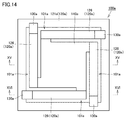
- FIG. 14 is a plan view showing the configuration of the piezoelectric transducer according to the modified example of the first embodiment of the present invention.
- FIG. 15 is a cross-sectional view of the piezoelectric transducer shown in FIG. 14 as seen from the direction of the arrow XV-XV.
- FIG. 16 is a cross-sectional view of the piezoelectric transducer shown in FIG. 14 as seen in the direction of arrows XVI-XVI.
- a piezoelectric transducer 100a As shown in FIGS. 14 to 16, a piezoelectric transducer 100a according to a modified example of the first embodiment of the present invention includes a base 110a, a plurality of beam portions 120a, a fixing portion 130a, and a plate-shaped portion 140a. There is.
- each of the plurality of beam portions 120a has an outer shape having a constant width in the extending direction when the piezoelectric transducer 100a is viewed from above. Specifically, each of the plurality of beam portions 120a has a rectangular outer shape when the piezoelectric transducer 100a is viewed from above.
- a piezoelectric transducer 100a includes four beam portions 120a. As shown in FIG. 14 and FIG. 16, each of the four beam portions 120a has a plurality of rectangular annular shapes inside the base portion 110a having a rectangular annular outer shape when the piezoelectric transducer 100a is viewed from above. It extends along the corresponding side of the sides. Each of the plurality of beam portions 120a extends while leaving a gap 101a having a substantially constant width with respect to the base portion 110a. Each of the plurality of beam portions 120a is located at the tip of the beam portion 120a with a gap 101a having a substantially constant width with respect to the adjacent beam portion 120a.
- the tip ends of the plurality of beam portions 120a opposite to the base portion 110a side are connected to the plate-shaped portion 140a. There is.
- the plate-shaped portion 140a is located inside the plurality of beam portions 120a when the piezoelectric transducer 100a is viewed from above.
- the plate portion 140a has a substantially rectangular outer shape.
- the plate portion 140a is connected to the beam portion 120a at the apex of the substantially rectangular shape.
- the plate-shaped portion 140a includes a piezoelectric layer 122a, a lower electrode layer 124a, and an active layer 125a, similarly to the end portion 121a of the beam portion 120a. Contains.
- the lower electrode layer 124a is arranged below the piezoelectric layer 122a.
- the active layer 125a is arranged below the lower electrode layer 124a.
- the piezoelectric layer 122a included in the plate-shaped portion 140a is continuous with the piezoelectric layer 122a included in each of the plurality of beam portions 120a.
- the lower electrode layer 124a included in the plate-shaped portion 140a is continuous with the lower electrode layer 124a included in each of the plurality of beam portions 120a.
- the active layer 125a included in the plate-shaped portion 140a is continuous with the active layer 125a included in each of the plurality of beam portions 120a.
- the plate-shaped portion 140a is continuous with each of the plurality of beam portions 120a.
- the plate-shaped portion 140a vertically vibrates together with the movable portion 126 of the beam portion 120a that is vertically displaced when the piezoelectric transducer 100a is driven.
- the fixing portion 130a is provided on the beam portion 120a so that the end portions 121a of the plurality of beam portions 120a are sandwiched between the base portion 110a. It is located in.
- the fixing portion 130a is positioned so as to overlap at least a part of the base portion 110a in the vertical direction, and extends so as to project from the base portion 110a in the extending direction of the beam portion 120a.
- the extension length of each of the plurality of beam portions 120a from above the base portion 110a is Lg, and the length of the movable portion 126 of each of the plurality of beam portions 120a is Lh.
- the piezoelectric transducer 100a temporarily above the base 110a of each of the plurality of beam portions 120a due to an alignment error between the processing of forming the gap 101a and the processing of forming the recess 102. Even when there is a difference in the extension length Lg from the above, it is possible to suppress the difference in the length Lh of the movable portion 126 of each of the plurality of beam portions 120a.
- the mechanical characteristics such as the resonance frequency and the amount of deformation of each of the plurality of beam portions 120a are made uniform, and the piezoelectric transducer 100a has the same structure.
- the input/output characteristics can be improved.
- the piezoelectric transducer according to the second exemplary embodiment of the present invention is different from the piezoelectric transducer 100 according to the first embodiment in the configuration of the fixing portion. Therefore, the description of the same configuration as the piezoelectric transducer 100 according to the first embodiment of the present invention will not be repeated.
- FIG. 17 is a plan view showing the configuration of the piezoelectric transducer according to the second embodiment of the present invention.
- the fixing portion 230 located on each of the plurality of beam portions 220 is formed of one member so as to be continuous with each other, and has an annular shape when viewed in the vertical direction. ing. Accordingly, the end portion 121 of each of the plurality of beam portions 220 can be stably and more firmly fixed by the fixing portion 230. As a result, the input/output characteristics of the piezoelectric transducer 200 can be stably improved.
- the piezoelectric transducer according to the third embodiment of the present invention will be described below.
- the piezoelectric transducer according to the third embodiment of the present invention is different from the piezoelectric transducer 100 according to the first embodiment of the present invention in the position where the fixing portion is arranged. Therefore, the description of the same configuration as the piezoelectric transducer 100 according to the first embodiment of the present invention will not be repeated.
- FIG. 18 is a cross-sectional view showing the configuration of the piezoelectric transducer according to the third embodiment of the present invention.
- the sectional view of the piezoelectric transducer 300 shown in FIG. 18 is shown in the same sectional view as the sectional view of the piezoelectric transducer 100 shown in FIG.
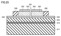
- the piezoelectric layer 322 is located closer to the tip end side of the beam 320 than the end 321 in the extending direction of the beam 320. It is located over the tip of the beam portion 320. That is, the piezoelectric layer 322 is not arranged above the base portion 310.
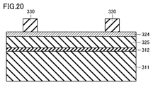
- the fixing portion 330 is arranged on the lower electrode layer 324.
- the end surface of the fixed portion 330 on the tip end side of the beam portion 320 and the end surface of the piezoelectric layer 322 on the end portion 321 side are in contact with each other.
- FIG. 19 is a cross-sectional view showing a state where a lower electrode layer is provided on the upper surface of the active layer in the method of manufacturing the piezoelectric transducer according to the third embodiment of the present invention.
- the lower electrode layer 324 is provided on the upper surface of the active layer 325 by a lift-off method, a plating method, an etching method, or the like.
- the stacked body including the lower base 311, the upper base 312, and the active layer 325 is prepared in advance as a so-called SOI substrate.
- FIG. 20 is a cross-sectional view showing a state in which a fixing portion is provided on the upper surface of the lower electrode layer in the method of manufacturing the piezoelectric transducer according to the third embodiment of the present invention.
- the fixing portion 330 is provided on the upper surface of the lower electrode layer 324 by a lift-off method, a plating method, an etching method, or the like.
- FIG. 21 is a cross-sectional view showing a state in which a piezoelectric layer is provided on the upper surface of the lower electrode layer in the method for manufacturing a piezoelectric transducer according to the third embodiment of the present invention.
- the piezoelectric layer 322 is provided on the upper surface of the lower electrode layer 324 by the CVD method, the PVD method, or the like.
- FIG. 22 is a cross-sectional view showing a state in which an upper electrode layer is provided on the upper surface of the piezoelectric layer in the method of manufacturing a piezoelectric transducer according to the third embodiment of the present invention.
- FIG. 23 is a diagram showing a state in which the upper electrode layer is patterned in the method for manufacturing a piezoelectric transducer according to the third embodiment of the present invention.
- an upper electrode layer 323 is provided on the upper surface of the piezoelectric layer 322 and a gap 301 is formed in the upper electrode layer 323 by a lift-off method, a plating method, an etching method, or the like.
- FIG. 24 is a diagram showing a state in which the piezoelectric layer is patterned in the method for manufacturing a piezoelectric transducer according to the third embodiment of the present invention.
- the piezoelectric layer 322 is patterned by a lift-off method or an etching method.
- the gap 301 is formed in the piezoelectric layer 322.
- FIG. 25 is a diagram showing a state in which the lower electrode layer is patterned in the method for manufacturing a piezoelectric transducer according to the third embodiment of the present invention.
- the lower electrode layer 324 is patterned by a lift-off method or an etching method. As a result, the gap 301 is formed in the lower electrode layer 324.
- FIG. 26 is a diagram showing a state where the active layer is patterned in the method for manufacturing a piezoelectric transducer according to the third embodiment of the present invention.
- the active layer 325 is patterned by a lift-off method or an etching method.
- the gap 301 is formed in the active layer 325.
- FIG. 27 is a diagram showing a state in which a recess is formed in the lower base in the method for manufacturing a piezoelectric transducer according to the third embodiment of the present invention.
- the recess 302 is formed in the lower base 311 by performing deep reactive ion etching or wet etching on the lower base 311 from the lower surface side of the lower base 311.
- the piezoelectric transducer 300 according to the third embodiment of the present invention as shown in FIG. 18 is manufactured.
- the fixing portion 330 is arranged on the lower electrode layer 324. Accordingly, since the piezoelectric layer 122 is not located below the fixing portion 330, the fixing portion 330 can stably fix the respective end portions 321 of the plurality of beam portions 320. As a result, the input/output characteristics of the piezoelectric transducer 300 can be stably improved.
- the piezoelectric transducer 300 it is assumed that the plurality of beam portions 320 are extended from above the base portion 310 due to an alignment error between the processing of forming the gap 301 and the processing of forming the recess 302. Even when there is a difference in the protruding length Li, it is possible to suppress the difference in the length Lj of the movable portion 126 of each of the plurality of beam portions 320.
- the length Lj of the movable portion 126 of each of the plurality of beam portions 320 uniform, the mechanical characteristics such as the resonance frequency and the deformation amount of each of the plurality of beam portions 320 are made uniform, and the piezoelectric transducer 300 of the piezoelectric transducer 300 is made.
- the input/output characteristics can be improved.
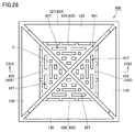
- the piezoelectric transducer according to the fourth embodiment of the present invention is different from the piezoelectric transducer 100 according to the first embodiment in the shape of the movable portion in each of the plurality of beam portions. Therefore, the description of the same configuration as the piezoelectric transducer 100 according to the first embodiment of the present invention will not be repeated.
- FIG. 28 is a plan view showing the configuration of the piezoelectric transducer according to the fourth embodiment of the present invention.
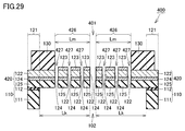
- FIG. 29 is a cross-sectional view of the piezoelectric transducer shown in FIG. 28 as seen from the direction of arrows along the line XXIX-XXIX.
- a plurality of through holes 427 penetrating the beam portion 420 in the vertical direction is formed in each of the plurality of beam portions 420. ing.
- Each of the plurality of through holes 427 is located closer to the tip end side of the beam portion 420 than the fixing portion 430 in the extending direction of the beam portion 420.
- each of the plurality of through holes 427 is located in the movable portion 426 of the beam portion 420. Accordingly, in each of the plurality of beam portions 420, the rigidity of the movable portion 426 becomes low, and the end portion 421 of each of the plurality of beam portions 420 can be stably fixed by the fixed portion 430. As a result, the input/output characteristics of the piezoelectric transducer 400 can be stably improved.
- the plurality of through holes 427 are arranged in each of the plurality of beam portions 420 so as to be symmetrical with respect to the extending direction of the beam portions 420.
- the plurality of through holes 427 in each of the plurality of beam portions 420 are arranged such that the shapes of the plurality of beam portions 420 are point-symmetric with respect to the virtual center point C of the piezoelectric transducer 400.
- the plurality of through holes 427 are formed at the time of patterning the gap 401, but the method of forming the plurality of through holes 427 is not limited to the above method and is a step different from the patterning of the gap 401. It may be formed by punching.
- the gaps 401 are formed and the recesses 102 are formed, an alignment error may occur between the bases 410 of the plurality of beam portions 420 from above. Even when there is a difference in the projected length Lk, it is possible to suppress the difference in the length Lm of the movable portions 126 of the plurality of beam portions 420.
- the mechanical characteristics such as the resonance frequency and the amount of deformation of each of the plurality of beam portions 420 are made uniform and the piezoelectric transducer 400 of the piezoelectric transducer 400 is made uniform.
- the input/output characteristics can be improved.
Abstract
End parts (121) of each of a plurality of beam parts (120) are supported by base parts (110), and each of the plurality of beam parts (120) extends in a direction away from the base parts (110) at positions further to the upper side than the base parts (110). Each of the plurality of beam parts (120) is formed from a plurality of layers. Each of the plurality of beam parts (120) comprises: a piezoelectric body layer (122); an upper electrode layer (123) which is positioned to the upper side of the piezoelectric body layer (122); and a lower electrode layer (124) which is positioned so as to face at least a portion of the upper electrode layer (123) with the piezoelectric body layer (122) sandwiched therebetween. Anchoring parts (130) are positioned above the beam parts (120) so as to sandwich the end parts (121) of each of the plurality of beam parts (120) between said anchoring parts (130) and the base parts (110). While being positioned so as to vertically overlap at least partially with the base parts (110), the anchoring parts (130) extend so as to protrude further than the base parts (110) in the extension direction of the beam parts (120).
Description
本発明は、圧電トランスデューサに関する。
The present invention relates to a piezoelectric transducer.
圧電トランスデューサの構成を開示した先行文献として、特表2014-515214号公報(特許文献1)がある。特許文献1に記載された圧電トランスデューサは、基板と、複数の片持ち梁とを備えている。複数の片持ち梁の各々は、互いに隣接し、先細である。複数の片持ち梁の各々は、梁基端部と、梁先端部と、梁本体部とを規定している。梁本体部は、梁基端部と梁先端部との間に配置される。複数の片持ち梁の各々は、梁先端部が共通の仮想点に向けて延びるように配置されている。複数の片持ち梁の各々は、梁基端部に沿って基板に結合されるが、梁本体部に沿って基板に結合されていない。
As a prior document disclosing the configuration of the piezoelectric transducer, there is Japanese Patent Publication No. 2014-515214 (Patent Document 1). The piezoelectric transducer described in Patent Document 1 includes a substrate and a plurality of cantilevers. Each of the plurality of cantilevers is adjacent to each other and is tapered. Each of the plurality of cantilever beams defines a beam base end portion, a beam tip end portion, and a beam main body portion. The beam main body portion is arranged between the beam base end portion and the beam tip end portion. Each of the plurality of cantilever beams is arranged so that the tip end portion of the beam extends toward a common virtual point. Each of the plurality of cantilevers is coupled to the substrate along the beam base end portion, but is not coupled to the substrate along the beam body portion.
従来の圧電トランスデューサにおいては、基板の表面側に、圧電体層などのパターンが形成される。また、基板の裏面側から、深掘反応性イオンエッチング(Deep RIE:Deep Reactive Ion Etching)またはウェットエッチングなどの加工が施されることにより、基板に凹部が設けられる。基板の表面側の加工時と裏面側の加工時とにおいてアライメント誤差が生じた場合、複数の梁部の各々の可動部の長さに差が生じる。これにより、圧電トランスデューサの駆動時に、複数の梁部の各々の共振周波数および変形量などの機械的特性が互いに異なるため、圧電トランスデューサの入出力特性が低下する。
In a conventional piezoelectric transducer, a pattern such as a piezoelectric layer is formed on the surface side of the substrate. Also, a recess is provided in the substrate by performing processing such as deep reactive ion etching (Deep RIE: Deep Reactive Ion Etching) or wet etching from the back surface side of the substrate. When an alignment error occurs between the processing of the front surface side and the processing of the back surface side of the substrate, a difference occurs in the length of the movable portion of each of the plurality of beam portions. As a result, when the piezoelectric transducer is driven, the mechanical characteristics such as the resonance frequency and the deformation amount of each of the plurality of beam portions are different from each other, so that the input/output characteristics of the piezoelectric transducer deteriorate.
本発明は、上記の問題点に鑑みてなされたものであって、複数の梁部の各々の可動部の長さを均一化することにより、入出力特性が向上された、圧電トランスデューサを提供することを目的とする。
The present invention has been made in view of the above problems, and provides a piezoelectric transducer in which the input/output characteristics are improved by making the lengths of the movable portions of the plurality of beam portions uniform. The purpose is to
本発明に基づく圧電トランスデューサは、基部と、複数の梁部と、少なくとも1つの固定部とを備えている。複数の梁部の各々は、基部に端部を支持されて、基部より上側の位置にて基部から離れる方向に延在している。複数の梁部の各々は、複数の層からなる。複数の梁部の各々は、圧電体層と、圧電体層の上側に配置された上部電極層と、圧電体層を挟んで上部電極層の少なくとも一部に対向するように配置された下部電極層とを含んでいる。固定部は、複数の梁部の各々の端部を基部と挟むように梁部上に配置されている。固定部は、上下方向において基部の少なくとも一部と重なるように位置しつつ、梁部の延在方向において、基部より突出するように延在している。
The piezoelectric transducer according to the present invention includes a base portion, a plurality of beam portions, and at least one fixing portion. Each of the plurality of beam portions has an end portion supported by the base portion, and extends at a position above the base portion in a direction away from the base portion. Each of the plurality of beam portions includes a plurality of layers. Each of the plurality of beam portions has a piezoelectric layer, an upper electrode layer disposed above the piezoelectric layer, and a lower electrode disposed so as to face at least a part of the upper electrode layer with the piezoelectric layer sandwiched therebetween. With layers. The fixing portion is arranged on the beam portion so as to sandwich each end of the plurality of beam portions with the base portion. The fixing portion is positioned so as to overlap at least a part of the base portion in the vertical direction, and extends so as to project from the base portion in the extending direction of the beam portion.
本発明によれば、複数の梁部の各々の可動部の長さを均一化することにより、圧電トランスデューサの入出力特性を向上することができる。
According to the present invention, the input/output characteristics of the piezoelectric transducer can be improved by making the lengths of the movable portions of the plurality of beam portions uniform.
以下、本発明の各実施形態に係る圧電トランスデューサについて図面を参照して説明する。以下の実施形態の説明においては、図中の同一または相当部分には同一符号を付して、その説明は繰り返さない。
A piezoelectric transducer according to each embodiment of the present invention will be described below with reference to the drawings. In the following description of the embodiments, the same or corresponding parts in the drawings will be denoted by the same reference numerals and the description thereof will not be repeated.
(実施形態1)
図1は、本発明の実施形態1に係る圧電トランスデューサの構成を示す平面図である。図2は、図1に示した圧電トランスデューサについてII-II線矢印方向から見た断面図である。 (Embodiment 1)
FIG. 1 is a plan view showing the configuration of the piezoelectric transducer according to the first embodiment of the present invention. FIG. 2 is a cross-sectional view of the piezoelectric transducer shown in FIG. 1 as seen in the direction of arrows II-II.
図1および図2に示すように、本発明の実施形態1に係る圧電トランスデューサ100は、基部110と、複数の梁部120と、少なくとも1つの固定部130とを備えている。本実施形態においては、4つの固定部130が設けられている。
As shown in FIGS. 1 and 2, the piezoelectric transducer 100 according to the first embodiment of the present invention includes a base portion 110, a plurality of beam portions 120, and at least one fixing portion 130. In this embodiment, four fixing parts 130 are provided.
図2に示すように、基部110は、複数の梁部120の各々の端部121の下側に位置している。このため、基部110は、図1に示す複数の梁部120の各々の端部121と同様に、圧電トランスデューサ100を上側から見たときに環状の外形を有しており、具体的には、矩形環状の外形を有している。
As shown in FIG. 2, the base portion 110 is located below the end portion 121 of each of the plurality of beam portions 120. Therefore, the base portion 110 has an annular outer shape when the piezoelectric transducer 100 is viewed from above, like the end portions 121 of each of the plurality of beam portions 120 shown in FIG. It has a rectangular annular outer shape.
図2に示すように、本実施形態において、基部110は、一定の幅で上下方向に延在する断面形状を有している。なお、基部110は、上側に向かうに従って幅が広くなる断面形状を有していてもよい。
As shown in FIG. 2, in the present embodiment, the base 110 has a cross-sectional shape that extends in the vertical direction with a constant width. In addition, the base 110 may have a cross-sectional shape in which the width becomes wider toward the upper side.
基部110は、下側基部111と上側基部112を含んでいる。上側基部112は、下側基部111の上部に積層されている。本実施形態において、下側基部111は、Siで構成されている。上側基部112はSiO2で構成されている。
The base 110 includes a lower base 111 and an upper base 112. The upper base 112 is stacked on the lower base 111. In the present embodiment, the lower base 111 is made of Si. The upper base 112 is made of SiO 2 .
図1および図2に示すように、複数の梁部120の各々は、基部110に端部121を支持されて、基部110より上側の位置にて基部110から離れる方向に延在している。
As shown in FIGS. 1 and 2, each of the plurality of beam portions 120 has an end portion 121 supported by the base portion 110 and extends in a direction above the base portion 110 and away from the base portion 110.
複数の梁部120の各々は、圧電トランスデューサ100を上側から見たときに、梁部120の延在方向において先細の外形を有している。具体的には、複数の梁部120の各々は、圧電トランスデューサ100を上側から見たときに、三角形状の外形を有している。本実施形態において、この三角形状は、二等辺三角形状である。
Each of the plurality of beam portions 120 has a tapered outer shape in the extending direction of the beam portion 120 when the piezoelectric transducer 100 is viewed from above. Specifically, each of the plurality of beam portions 120 has a triangular outer shape when the piezoelectric transducer 100 is viewed from above. In the present embodiment, this triangular shape is an isosceles triangular shape.
なお、複数の梁部120の各々は、圧電トランスデューサ100を上側から見たときに、梁部120の延在方向において幅が一定となる外形を有してもよいし、梁部120の延在方向において幅が徐々に広くなるような外形を有してもよい。複数の梁部120の各々は、矩形状の外形を有していてもよい。梁部120の形状および配置が異なる変形例に係る圧電トランスデューサについては、後述する。
Note that each of the plurality of beam portions 120 may have an outer shape having a constant width in the extending direction of the beam portion 120 when the piezoelectric transducer 100 is viewed from above, or the extension of the beam portion 120. It may have an outer shape in which the width gradually increases in the direction. Each of the plurality of beam portions 120 may have a rectangular outer shape. A piezoelectric transducer according to a modified example in which the shape and arrangement of the beam portion 120 are different will be described later.
図1に示すように、本実施形態においては、圧電トランスデューサは4つの梁部120を備えている。複数の梁部120の各々は、圧電トランスデューサ100を上側から見たときに、圧電トランスデューサ100の仮想中心点Cに関して互いに点対称となるように配置されている。本実施形態においては、4つの梁部120の各々は、圧電トランスデューサ100を上側から見たときに、互いに異なる方向に延在しつつ隣接する梁部120同士の延在方向が互いに90°異なるように、配置されている。
As shown in FIG. 1, in the present embodiment, the piezoelectric transducer includes four beam portions 120. Each of the plurality of beam portions 120 is arranged so as to be point-symmetric with respect to the virtual center point C of the piezoelectric transducer 100 when the piezoelectric transducer 100 is viewed from above. In the present embodiment, when the piezoelectric transducer 100 is viewed from above, each of the four beam portions 120 extends in different directions, and the extending directions of the adjacent beam portions 120 are different from each other by 90°. It is located in.
本実施形態において、複数の梁部120の延在方向は、圧電トランスデューサ100を上側から見たときに、仮想中心点Cに向かって延在している。なお、複数の梁部120の各々の延在方向は、仮想中心点から離れるように延在してもよいし、仮想中心点Cに向かっていなくてもよい。
In the present embodiment, the extending direction of the plurality of beam portions 120 extends toward the virtual center point C when the piezoelectric transducer 100 is viewed from above. The extending direction of each of the plurality of beam portions 120 may extend away from the virtual center point, or may not extend toward the virtual center point C.
図1および図2に示すように、複数の梁部120の各々は、隣接する梁部120の端部121同士が互いに連続するように構成されている。このように、複数の梁部120の各々の端部121は、連続するように構成されており、圧電トランスデューサ100を上側から見たときに、環状の外形を有しており、具体的には、矩形環状の外形を有している。
As shown in FIGS. 1 and 2, each of the plurality of beam portions 120 is configured such that the end portions 121 of the adjacent beam portions 120 are continuous with each other. As described above, the end 121 of each of the plurality of beam portions 120 is configured to be continuous, and has an annular outer shape when the piezoelectric transducer 100 is viewed from the upper side. , Has a rectangular annular outer shape.
複数の梁部120の各々は、隙間101を挟んで、互いに離れて位置している。本実施形態において、複数の梁部120同士の間に位置する隙間101は、圧電トランスデューサ100を上側から見たときに、仮想中心点Cから放射状に延在している。隙間101の延在する方向において、隙間101の幅は略一定である。
Each of the plurality of beam portions 120 is located apart from each other with the gap 101 interposed therebetween. In the present embodiment, the gaps 101 located between the plurality of beam portions 120 extend radially from the virtual center point C when the piezoelectric transducer 100 is viewed from above. The width of the gap 101 is substantially constant in the direction in which the gap 101 extends.
図1および図2に示すように、本実施形態において、複数の梁部120の各々の先端部は、基部110から離間した自由端である。なお、複数の梁部120の各々の先端部は、圧電トランスデューサ100の駆動時に上下に振動する板状部と互いに接続されていてもよい。板状部を備える、変形例に係る圧電トランスデューサについては、後述する。
As shown in FIGS. 1 and 2, in the present embodiment, the tip ends of the plurality of beam portions 120 are free ends that are separated from the base portion 110. Note that the tip ends of the plurality of beam portions 120 may be connected to a plate-like portion that vibrates up and down when the piezoelectric transducer 100 is driven. The piezoelectric transducer according to the modified example including the plate-shaped portion will be described later.
図2に示すように、複数の梁部120の各々は、複数の層からなる。複数の梁部120の各々は、圧電体層122と、上部電極層123と、下部電極層124とを含んでいる。
As shown in FIG. 2, each of the plurality of beam portions 120 is composed of a plurality of layers. Each of the plurality of beam portions 120 includes a piezoelectric layer 122, an upper electrode layer 123, and a lower electrode layer 124.
本実施形態において、圧電体層122は、梁部120の延在方向において端部121側から先端部側までの全長にわたって配置されている。また、圧電体層122は、梁部120の延在方向に直交する幅方向の全体にわたって配置されている。
In the present embodiment, the piezoelectric layer 122 is arranged over the entire length from the end 121 side to the tip side in the extending direction of the beam 120. Further, the piezoelectric layer 122 is arranged over the entire width direction orthogonal to the extending direction of the beam 120.
圧電体層122は、多結晶材料で構成されてもよいし、単結晶材料で構成されていてもよい。圧電体層122は、チタン酸ジルコン酸鉛(PZT)系のセラミックス、窒化アルミニウム(AlN)、ニオブ酸リチウム(LiNbO3)またはタンタル酸リチウム(LiTaO3)などで構成されている。
The piezoelectric layer 122 may be made of a polycrystalline material or a single crystal material. The piezoelectric layer 122 is made of lead zirconate titanate (PZT)-based ceramics, aluminum nitride (AlN), lithium niobate (LiNbO 3 ), lithium tantalate (LiTaO 3 ), or the like.
本実施形態において、上部電極層123は、圧電体層122の上側に配置されている。上部電極層123は、梁部120の延在方向において、梁部120の端部121より先端部側の部分から、先端部にかけて配置されている。また、上部電極層123は、圧電トランスデューサ100を上側から見たときに、梁部120の延在方向に直交する幅方向の全体にわたって配置されている。
In the present embodiment, the upper electrode layer 123 is arranged above the piezoelectric layer 122. The upper electrode layer 123 is arranged in the extending direction of the beam portion 120 from a portion closer to the tip portion than the end portion 121 of the beam portion 120 to the tip portion. Further, the upper electrode layer 123 is arranged over the entire width direction orthogonal to the extending direction of the beam 120 when the piezoelectric transducer 100 is viewed from above.
上部電極層123は、Ptなどの導電性を有する材料で構成されている。上部電極層123と圧電体層122との間に、Tiなどで構成された密着層が配置されていてもよい。
The upper electrode layer 123 is made of a conductive material such as Pt. An adhesion layer made of Ti or the like may be arranged between the upper electrode layer 123 and the piezoelectric layer 122.
下部電極層124は、圧電体層122を挟んで上部電極層123の少なくとも一部に対向するように配置されている。本実施形態において、下部電極層124は、梁部120の延在方向において、梁部120の端部121側から先端部側までの全長にわたって配置されている。また、下部電極層124は、梁部120の延在方向に直交する幅方向の全体にわたって位置している。
The lower electrode layer 124 is arranged so as to face at least a part of the upper electrode layer 123 with the piezoelectric layer 122 interposed therebetween. In the present embodiment, the lower electrode layer 124 is arranged over the entire length from the end 121 side of the beam 120 to the tip side in the extending direction of the beam 120. Further, the lower electrode layer 124 is located over the entire width direction orthogonal to the extending direction of the beam 120.
下部電極層124は、Ptなどの導電性を有する材料で構成されている。下部電極層124と基部110との間に、Tiなどで構成された密着層が配置されていてもよい。
The lower electrode layer 124 is made of a conductive material such as Pt. An adhesion layer made of Ti or the like may be disposed between the lower electrode layer 124 and the base 110.
本実施形態において、複数の梁部120の各々は、下部電極層124の下側に、活性層125をさらに含んでいる。活性層125は、梁部120の延在方向において、梁部120の端部121側から先端部側までの全長にわたって配置されている。また、活性層125は、梁部120の延在方向に直交する幅方向の全体にわたって位置している。
In the present embodiment, each of the plurality of beam portions 120 further includes an active layer 125 below the lower electrode layer 124. The active layer 125 is arranged over the entire length from the end 121 side of the beam 120 to the tip side in the extending direction of the beam 120. Further, the active layer 125 is located over the entire width direction orthogonal to the extending direction of the beam 120.
本実施形態において、活性層125はSiで構成されている。活性層125は、電気絶縁性を有する材料で構成されていてもよい。下部電極層124と活性層125との間に、Tiなどで構成された密着層が配置されていてもよい。
In this embodiment, the active layer 125 is made of Si. The active layer 125 may be made of a material having electrical insulation. An adhesion layer made of Ti or the like may be disposed between the lower electrode layer 124 and the active layer 125.
図1および図2に示すように、固定部130は、複数の梁部120の各々の端部121を基部110と挟むように梁部120上に配置されている。固定部130は、上下方向において基部110の少なくとも一部と重なるように位置しつつ、梁部120の延在方向において、基部110より突出するように延在している。複数の固定部130の各々は、上下方向から見て、隙間101を挟んで互いに離れて位置しつつ、仮想環上に延在するように配置されている。
As shown in FIGS. 1 and 2, the fixing portion 130 is arranged on the beam portion 120 so as to sandwich each end 121 of the plurality of beam portions 120 with the base portion 110. The fixing portion 130 is positioned so as to overlap at least a part of the base portion 110 in the vertical direction, and extends so as to project from the base portion 110 in the extending direction of the beam portion 120. Each of the plurality of fixing portions 130 is arranged so as to extend on the virtual ring while being located apart from each other with the gap 101 interposed therebetween when viewed in the vertical direction.
本実施形態においては、圧電トランスデューサ100を上側から見たときに、梁部120の先端部側とは反対側に位置する固定部130の端面は、梁部120の先端部側とは反対側に位置する梁部120の端面より、梁部120の先端部側に位置しているが、梁部120の当該端面と重なるように位置していてもよい。
In the present embodiment, when the piezoelectric transducer 100 is viewed from above, the end surface of the fixing portion 130 located on the side opposite to the tip end side of the beam portion 120 is on the side opposite to the tip end side of the beam portion 120. Although it is located closer to the tip end side of the beam section 120 than the end surface of the beam section 120 that is located, it may be located so as to overlap the end surface of the beam section 120.
本実施形態においては、圧電トランスデューサ100を上側から見たときに、梁部120において、梁部120の先端部側の固定部130の端面が位置する部分から、梁部120の先端部までの領域が、可動部126となる。
In the present embodiment, when the piezoelectric transducer 100 is viewed from the upper side, in the beam portion 120, a region from the portion where the end surface of the fixed portion 130 on the tip end side of the beam portion 120 is located to the tip portion of the beam portion 120. Becomes the movable part 126.
また、本実施形態において、固定部130は、圧電体層122上に配置されている。さらに、圧電トランスデューサ100を上側から見たときに、固定部130は、上部電極層123と重ならないように配置されている。固定部130における梁部120の先端部側の端面と、上部電極層123の基部110側の端面とは、互いに接触している。
Further, in the present embodiment, the fixed portion 130 is arranged on the piezoelectric layer 122. Furthermore, when the piezoelectric transducer 100 is viewed from the upper side, the fixing portion 130 is arranged so as not to overlap the upper electrode layer 123. The end surface of the fixed portion 130 on the tip end side of the beam portion 120 and the end surface of the upper electrode layer 123 on the base portion 110 side are in contact with each other.
なお、固定部130は、上部電極層123上に配置されていてもよい。この場合、固定部130における梁部120の先端部側の端面と、上部電極層123の基部110側の端面との位置合わせを不要とすることができる。
Note that the fixed part 130 may be arranged on the upper electrode layer 123. In this case, it is not necessary to align the end surface of the fixed portion 130 on the tip end side of the beam 120 with the end surface of the upper electrode layer 123 on the base 110 side.
本実施形態において、固定部130は、上部電極層123を構成する材料とは異なる材料で構成されている。上部電極層123を構成する材料とは反応しないエッチャントを用いて固定部130をエッチングすることにより、上部電極層123の形状を変化させることなく、固定部130をパターニングすることができる。
In this embodiment, the fixing portion 130 is made of a material different from the material forming the upper electrode layer 123. By etching the fixing portion 130 using an etchant that does not react with the material forming the upper electrode layer 123, the fixing portion 130 can be patterned without changing the shape of the upper electrode layer 123.
また、固定部130を構成する材料は複数の梁部120を構成する材料より硬く、本実施形態において、固定部130を構成する材料は、圧電体層122を構成する材料および上部電極層123を構成する材料の各々よりヤング率が高い。具体的には、固定部130を構成する材料のヤング率は200GPa以上である。固定部130は、金属材料から構成されていてもよいし、非金属材料で構成されていてもよい。ただし、固定部130が上部電極層123または下部電極層124に接する場合は、固定部130は非金属材料で構成される。
Further, the material forming the fixing portion 130 is harder than the material forming the plurality of beam portions 120, and in the present embodiment, the material forming the fixing portion 130 includes the material forming the piezoelectric layer 122 and the upper electrode layer 123. Young's modulus is higher than each of the constituent materials. Specifically, the Young's modulus of the material forming the fixing portion 130 is 200 GPa or more. The fixing portion 130 may be made of a metal material or a non-metal material. However, when the fixed part 130 contacts the upper electrode layer 123 or the lower electrode layer 124, the fixed part 130 is made of a non-metallic material.
図2に示すように、本実施形態に係る圧電トランスデューサ100は、後述する積層体に対して下面側から凹部102が設けられることで、基部110と梁部120とが形成される。以下、本発明の実施形態1に係る圧電トランスデューサ100の製造方法について説明する。
As shown in FIG. 2, in the piezoelectric transducer 100 according to the present embodiment, the base portion 110 and the beam portion 120 are formed by providing the recessed portion 102 from the lower surface side with respect to the laminated body described later. Hereinafter, a method for manufacturing the piezoelectric transducer 100 according to the first embodiment of the present invention will be described.
図3は、本発明の実施形態1に係る圧電トランスデューサの製造方法において、活性層の上面に下部電極層を設けた状態を示す断面図である。図3に示すように、リフトオフ法、めっき法、または、エッチング法などにより、活性層125の上面に下部電極層124を設ける。
FIG. 3 is a cross-sectional view showing a state where a lower electrode layer is provided on the upper surface of the active layer in the method of manufacturing the piezoelectric transducer according to the first embodiment of the present invention. As shown in FIG. 3, the lower electrode layer 124 is provided on the upper surface of the active layer 125 by a lift-off method, a plating method, an etching method, or the like.
なお、本実施形態において、下側基部111、上側基部112および活性層125を有する積層体は、いわゆるSOI(Silicon on Insulator)基板として予め準備される。
In the present embodiment, the laminated body having the lower base 111, the upper base 112 and the active layer 125 is prepared in advance as a so-called SOI (Silicon on Insulator) substrate.
図4は、本発明の実施形態1に係る圧電トランスデューサの製造方法において、下部電極層の上面に圧電体層を設けた状態を示す断面図である。図4に示すように、CVD(Chemical Vapor Deposition)法またはPVD(Physical Vapor Deposition)法などにより、下部電極層124の上面に、圧電体層122を設ける。
FIG. 4 is a cross-sectional view showing a state in which a piezoelectric layer is provided on the upper surface of the lower electrode layer in the method of manufacturing the piezoelectric transducer according to the first embodiment of the present invention. As shown in FIG. 4, the piezoelectric layer 122 is provided on the upper surface of the lower electrode layer 124 by a CVD (Chemical Vapor Deposition) method, a PVD (Physical Vapor Deposition) method, or the like.
図5は、本発明の実施形態1に係る圧電トランスデューサの製造方法において、圧電体層の上面に上部電極層を設けた状態を示す断面図である。図6は、本発明の実施形態1に係る圧電トランスデューサの製造方法において、上部電極層をパターニングした状態を示す図である。
FIG. 5 is a cross-sectional view showing a state in which an upper electrode layer is provided on the upper surface of the piezoelectric layer in the method of manufacturing the piezoelectric transducer according to the first embodiment of the present invention. FIG. 6 is a diagram showing a state in which the upper electrode layer is patterned in the method of manufacturing the piezoelectric transducer according to the first embodiment of the present invention.
図5および図6に示すように、リフトオフ法、めっき法、または、エッチング法などにより、圧電体層122の上面に上部電極層123を設けるとともに、上部電極層123をパターニングする。これにより、上部電極層123において隙間101が形成される。
As shown in FIGS. 5 and 6, the upper electrode layer 123 is provided on the upper surface of the piezoelectric layer 122 and the upper electrode layer 123 is patterned by a lift-off method, a plating method, an etching method, or the like. As a result, the gap 101 is formed in the upper electrode layer 123.
図7は、本発明の実施形態1に係る圧電トランスデューサの製造方法において、圧電体層をパターニングした状態を示す図である。図7に示すように、リフトオフ法またはエッチング法などにより、圧電体層122をパターニングする。これにより、圧電体層122において隙間101が形成される。
FIG. 7 is a diagram showing a state in which the piezoelectric layer is patterned in the method for manufacturing a piezoelectric transducer according to the first embodiment of the present invention. As shown in FIG. 7, the piezoelectric layer 122 is patterned by a lift-off method or an etching method. As a result, the gap 101 is formed in the piezoelectric layer 122.
図8は、本発明の実施形態1に係る圧電トランスデューサの製造方法において、下部電極層をパターニングした状態を示す図である。図8に示すように、リフトオフ法またはエッチング法などにより、下部電極層124をパターニングする。これにより、下部電極層124において隙間101が形成される。
FIG. 8 is a diagram showing a state in which the lower electrode layer is patterned in the method for manufacturing a piezoelectric transducer according to the first embodiment of the present invention. As shown in FIG. 8, the lower electrode layer 124 is patterned by a lift-off method or an etching method. As a result, the gap 101 is formed in the lower electrode layer 124.
図9は、本発明の実施形態1に係る圧電トランスデューサの製造方法において、活性層をパターニングした状態を示す図である。図9に示すように、リフトオフ法またはエッチング法などにより、活性層125をパターニングする。これにより、活性層125において隙間101が形成される。
FIG. 9 is a diagram showing a state in which the active layer is patterned in the method of manufacturing the piezoelectric transducer according to the first embodiment of the present invention. As shown in FIG. 9, the active layer 125 is patterned by a lift-off method or an etching method. As a result, the gap 101 is formed in the active layer 125.
図10は、本発明の実施形態1に係る圧電トランスデューサの製造方法において、圧電体層の上面に固定部が設けられた状態を示す図である。図10に示すように、リフトオフ法、メッキ法またはエッチング法などにより、圧電体層122の上面に固定部130を設ける。
FIG. 10 is a diagram showing a state in which the fixing portion is provided on the upper surface of the piezoelectric layer in the method for manufacturing the piezoelectric transducer according to the first embodiment of the present invention. As shown in FIG. 10, the fixing portion 130 is provided on the upper surface of the piezoelectric layer 122 by a lift-off method, a plating method, an etching method, or the like.
図11は、本発明の実施形態1に係る圧電トランスデューサの製造方法において、下側基部に凹部が形成された状態を示す図である。図11に示すように、下側基部111の下面側から下側基部111に対して深掘反応性イオンエッチングまたはウェットエッチングなどをすることにより、下側基部111において凹部102が形成される。
FIG. 11 is a diagram showing a state in which a recess is formed in the lower base in the method for manufacturing a piezoelectric transducer according to the first embodiment of the present invention. As shown in FIG. 11, the recess 102 is formed in the lower base 111 by performing deep reactive ion etching or wet etching from the lower surface side of the lower base 111 to the lower base 111.
さらに、上側基部112の下面側から上側基部112に対して深掘反応性イオンエッチングまたはウェットエッチングなどをすることにより、上側基部112において凹部102が形成される。これらの工程により、図2に示すような本発明の実施形態1に係る圧電トランスデューサ100が製造される。
Further, the recess 102 is formed in the upper base 112 by performing deep reactive ion etching or wet etching from the lower surface side of the upper base 112 to the upper base 112. Through these steps, the piezoelectric transducer 100 according to Embodiment 1 of the present invention as shown in FIG. 2 is manufactured.
図2においては、隙間101を形成する加工時と、凹部102を形成する加工時とのアライメント誤差が生じていない状態を図示している。そのため、図2においては、圧電トランスデューサ100の上下方向から見たときに、複数の梁部120の各々の基部110の上方からの延出長さLaが互いに略同一となっており、複数の梁部120の各々の可動部の長さLbが互いに略同一となっている。
FIG. 2 illustrates a state in which an alignment error does not occur between the processing for forming the gap 101 and the processing for forming the recess 102. Therefore, in FIG. 2, when viewed from above and below in the piezoelectric transducer 100, the extension lengths La of the plurality of beam portions 120 from above the respective base portions 110 are substantially the same, and the plurality of beam portions 120 are substantially the same. The lengths Lb of the movable parts of the parts 120 are substantially the same.
本実施形態に係る圧電トランスデューサ100においては、仮に、隙間101を形成する加工時と、凹部102を形成する加工時とのアライメント誤差によって、複数の梁部120の各々の基部110の上方からの延出長さに差が生じた場合においても、複数の梁部120の各々の可動部の長さに差が生じることを抑制することができる。
In the piezoelectric transducer 100 according to the present embodiment, it is assumed that the plurality of beam portions 120 are extended from above the base 110 due to an alignment error between the processing for forming the gap 101 and the processing for forming the recess 102. Even if there is a difference in the projected length, it is possible to suppress the difference in the lengths of the movable portions of the plurality of beam portions 120.
以下、本発明の実施形態1の実施例に係る圧電トランスデューサと、固定部130が設けられていない点のみ本発明の実施形態1に係る圧電トランスデューサとは異なる比較例に係る圧電トランスデューサとについて、上記アライメント誤差による影響の違いについて説明する。
Hereinafter, regarding the piezoelectric transducer according to the example of the first embodiment of the present invention and the piezoelectric transducer according to the comparative example, which is different from the piezoelectric transducer according to the first embodiment of the present invention only in that the fixing portion 130 is not provided, The difference in the influence of the alignment error will be described.
図12は、実施例に係る圧電トランスデューサの断面図である。図12に示す圧電トランスデューサ100xの断面図は、図2に示す圧電トランスデューサ100の断面図と同一の断面視にて図示している。
FIG. 12 is a cross-sectional view of the piezoelectric transducer according to the example. The sectional view of the piezoelectric transducer 100x shown in FIG. 12 is shown in the same sectional view as the sectional view of the piezoelectric transducer 100 shown in FIG.
図12に示すように、実施例に係る圧電トランスデューサ100xにおいては、隙間101を形成する加工時と、凹部102xを形成する加工時とのアライメント誤差が生じているため、複数の梁部120xの各々について、基部110xの上方からの延出長さが互いに異なる。たとえば、複数の梁部120xのうち、一の梁部120xにおける基部110xの上方からの延出長さがLcであり、他の梁部120xにおける基部110xの上方からの延出長さがLdであり、Lc<Ldである。
As shown in FIG. 12, in the piezoelectric transducer 100x according to the example, since an alignment error occurs during processing for forming the gap 101 and during processing for forming the recess 102x, each of the plurality of beam portions 120x is formed. The extension lengths of the base 110x from above are different from each other. For example, of the plurality of beam portions 120x, the extension length of one beam portion 120x from above the base portion 110x is Lc, and the extension length of the other beam portion 120x from above the base portion 110x is Ld. Yes, Lc<Ld.
実施例に係る圧電トランスデューサ100xは、固定部130xを備えている。固定部130xは、上下方向において基部110xの少なくとも一部と重なるように位置しつつ、梁部120xの延在方向において、基部110xより突出するように延在している。図12に示すように、複数の梁部120xの各々において固定部130xが設けられている部分は、固定部130xによって固定されるため、梁部120xの先端部側の固定部130xの端面の位置が可動部126xの固定端となる。
The piezoelectric transducer 100x according to the example includes a fixed portion 130x. The fixing portion 130x is positioned so as to overlap at least a part of the base portion 110x in the vertical direction, and extends so as to project from the base portion 110x in the extending direction of the beam portion 120x. As shown in FIG. 12, the portion of each of the plurality of beam portions 120x where the fixing portion 130x is provided is fixed by the fixing portion 130x, and therefore the position of the end surface of the fixing portion 130x on the tip end side of the beam portion 120x. Is the fixed end of the movable portion 126x.
固定部130xを形成する加工時には、隙間101を形成する加工時と同様に、圧電トランスデューサ100xの表面側からアライメントするため、凹部102xを形成する加工時の両面アライナする場合に比較して、アライメント誤差が生じにくい。そのため、アライメント誤差によって固定部130xの形成位置にばらつきが生じることを抑制することができる。その結果、仮に、複数の梁部120xの各々について、基部110xの上方からの延出長さが互いに異なっている場合においても、複数の梁部120xの各々の可動部の長さLbを互いに略同一に維持することができる。
Since alignment is performed from the front surface side of the piezoelectric transducer 100x during the processing for forming the fixed portion 130x, as in the processing for forming the gap 101, an alignment error compared to the case of double-side aligner during the processing for forming the recess 102x. Is less likely to occur. Therefore, it is possible to prevent the formation position of the fixed portion 130x from being varied due to an alignment error. As a result, even if the extension lengths of the plurality of beam portions 120x from above the base portion 110x are different from each other, the lengths Lb of the movable portions of the plurality of beam portions 120x are substantially the same. Can stay the same.
これにより、図12に示すように、実施例に係る圧電トランスデューサ100xの駆動時においては、点線で囲んだ領域で示したように、複数の梁部120xの可動部126xの各々を均一に変形させることができる。
As a result, as shown in FIG. 12, when the piezoelectric transducer 100x according to the embodiment is driven, each of the movable portions 126x of the plurality of beam portions 120x is uniformly deformed as shown by the area surrounded by the dotted line. be able to.
図13は、比較例に係る圧電トランスデューサの断面図である。図13に示す圧電トランスデューサ900の断面図は、図2に示す圧電トランスデューサ100の断面図と同一の断面視にて図示している。
FIG. 13 is a cross-sectional view of a piezoelectric transducer according to a comparative example. The sectional view of the piezoelectric transducer 900 shown in FIG. 13 is shown in the same sectional view as the sectional view of the piezoelectric transducer 100 shown in FIG.
図13に示すように、比較例に係る圧電トランスデューサ900においては、隙間101を形成する加工時と、凹部902を形成する加工時とのアライメント誤差が生じているため、複数の梁部920の各々について、基部910の上方からの延出長さが互いに異なる。たとえば、複数の梁部920のうち、一の梁部920における基部910の上方からの延出長さがLeであり、他の梁部920における基部910の上方からの延出長さがLfであり、Le<Lfである。
As shown in FIG. 13, in the piezoelectric transducer 900 according to the comparative example, there is an alignment error between the processing for forming the gap 101 and the processing for forming the recess 902, and thus each of the plurality of beam portions 920 is formed. The extension lengths from above the base portion 910 are different from each other. For example, among the plurality of beam portions 920, the extension length of the one beam portion 920 from above the base portion 910 is Le, and the extension length of the other beam portion 920 from above the base portion 910 is Lf. Yes, Le<Lf.
比較例に係る圧電トランスデューサ900においては、梁部920のうち、基部910の上方から延出している部分の全てが可動部926となる。このため、梁部920の先端部側の基部910の端面の位置が可動部926の固定端となる。その結果、複数の可動部926の各々の長さが互いに異なる。よって、上記の一の梁部920の可動部926の長さはLeとなり、他の梁部920の可動部926の長さはLfとなり、Le<Lfである。
In the piezoelectric transducer 900 according to the comparative example, all of the beam portion 920 extending from above the base portion 910 becomes the movable portion 926. Therefore, the position of the end surface of the base portion 910 on the tip end side of the beam portion 920 becomes the fixed end of the movable portion 926. As a result, the lengths of the plurality of movable portions 926 are different from each other. Therefore, the length of the movable portion 926 of the one beam portion 920 is Le, the length of the movable portion 926 of the other beam portion 920 is Lf, and Le<Lf.
これにより、図13に示すように、比較例に係る圧電トランスデューサ900の駆動時においては、点線で囲んだ領域で示したように、複数の梁部920の可動部926の各々を互いに均一に変形させることができない。
As a result, as shown in FIG. 13, when the piezoelectric transducer 900 according to the comparative example is driven, each of the movable portions 926 of the plurality of beam portions 920 is uniformly deformed as shown by the area surrounded by the dotted line. I can't let you.
上記のように、本発明の実施形態1に係る圧電トランスデューサ100においては、固定部130は、複数の梁部120の各々の端部121を基部110と挟むように梁部120上に配置されている。固定部130は、上下方向において基部110の少なくとも一部と重なるように位置しつつ、梁部120の延在方向において、基部110より突出するように延在している。
As described above, in the piezoelectric transducer 100 according to the first embodiment of the present invention, the fixing portion 130 is arranged on the beam portion 120 so as to sandwich each end 121 of the plurality of beam portions 120 with the base portion 110. There is. The fixing portion 130 is positioned so as to overlap at least a part of the base portion 110 in the vertical direction, and extends so as to project from the base portion 110 in the extending direction of the beam portion 120.
複数の梁部120の各々の可動部126の長さを均一化することにより、複数の梁部120の各々の共振周波数および変形量などの機械的特性を互いに均一にして、圧電トランスデューサ100の入出力特性を向上することができる。
By equalizing the lengths of the movable portions 126 of the plurality of beam portions 120, the mechanical characteristics such as the resonance frequency and the amount of deformation of the plurality of beam portions 120 are made uniform, and the piezoelectric transducer 100 is inserted. The output characteristics can be improved.
本実施形態に係る圧電トランスデューサ100においては、固定部130は、圧電体層122上に配置されている。
In the piezoelectric transducer 100 according to this embodiment, the fixed portion 130 is arranged on the piezoelectric layer 122.
これにより、固定部130の下方に上部電極層123と下部電極層124とに挟まれた圧電体層122が位置していないため、固定部130によって複数の梁部120の各々の端部121を安定して固定することができる。その結果、圧電トランスデューサ100の入出力特性を安定して向上することができる。
As a result, since the piezoelectric layer 122 sandwiched between the upper electrode layer 123 and the lower electrode layer 124 is not located below the fixing portion 130, the fixing portion 130 removes each end 121 of each of the plurality of beam portions 120. It can be fixed stably. As a result, the input/output characteristics of the piezoelectric transducer 100 can be stably improved.
本実施形態に係る圧電トランスデューサ100においては、固定部130を構成する材料は、圧電体層122を構成する材料および上部電極層123を構成する材料の各々よりヤング率が高い。
In the piezoelectric transducer 100 according to this embodiment, the material forming the fixed portion 130 has a higher Young's modulus than each of the material forming the piezoelectric layer 122 and the material forming the upper electrode layer 123.
これにより、圧電トランスデューサ100の駆動時において、梁部120の可動部126が変位する際に、固定部130によって梁部120の端部121をより強固に固定することができる。
Thereby, when the piezoelectric transducer 100 is driven, when the movable part 126 of the beam part 120 is displaced, the end part 121 of the beam part 120 can be more firmly fixed by the fixing part 130.
次に、本発明の実施形態1の変形例に係る圧電トランスデューサについて図を参照して説明する。なお、本発明の実施形態1の変形例に係る圧電トランスデューサは、板状部を備えるとともに、複数の梁部の各々が、矩形状であり、仮想中心点Cに向かって延在していない点が主に、本発明の実施形態1に係る圧電トランスデューサ100と異なるため、本発明の実施形態1に係る圧電トランスデューサ100と同様である構成については説明を繰り返さない。
Next, a piezoelectric transducer according to a modified example of the first embodiment of the present invention will be described with reference to the drawings. The piezoelectric transducer according to the modified example of Embodiment 1 of the present invention includes a plate-shaped portion, and each of the plurality of beam portions has a rectangular shape and does not extend toward the virtual center point C. However, since it is mainly different from the piezoelectric transducer 100 according to the first embodiment of the present invention, the description of the same configuration as the piezoelectric transducer 100 according to the first embodiment of the present invention will not be repeated.
図14は、本発明の実施形態1の変形例に係る圧電トランスデューサの構成を示す平面図である。図15は、図14に示した圧電トランスデューサをXV-XV線矢印方向から見た断面図である。図16は、図14に示した圧電トランスデューサをXVI-XVI線矢印方向から見た断面図である。
FIG. 14 is a plan view showing the configuration of the piezoelectric transducer according to the modified example of the first embodiment of the present invention. FIG. 15 is a cross-sectional view of the piezoelectric transducer shown in FIG. 14 as seen from the direction of the arrow XV-XV. FIG. 16 is a cross-sectional view of the piezoelectric transducer shown in FIG. 14 as seen in the direction of arrows XVI-XVI.
図14から図16に示すように、本発明の実施形態1の変形例に係る圧電トランスデューサ100aは、基部110aと、複数の梁部120aと、固定部130aと、板状部140aとを備えている。
As shown in FIGS. 14 to 16, a piezoelectric transducer 100a according to a modified example of the first embodiment of the present invention includes a base 110a, a plurality of beam portions 120a, a fixing portion 130a, and a plate-shaped portion 140a. There is.
図14に示すように、複数の梁部120aの各々は、圧電トランスデューサ100aを上側から見たときに、延在方向において幅が一定となる外形を有している。具体的には、複数の梁部120aの各々は、圧電トランスデューサ100aを上側から見たときに、矩形状の外形を有している。
As shown in FIG. 14, each of the plurality of beam portions 120a has an outer shape having a constant width in the extending direction when the piezoelectric transducer 100a is viewed from above. Specifically, each of the plurality of beam portions 120a has a rectangular outer shape when the piezoelectric transducer 100a is viewed from above.
本実施形態の変形例に係る圧電トランスデューサ100aは、4つの梁部120aを備えている。図14および図16に示すように、4つの梁部120aの各々は、圧電トランスデューサ100aを上側から見たときに、矩形環状の外形を有する基部110aの内側において、上記矩形環状を構成する複数の辺のうち対応する辺に沿うように延在している。複数の梁部120aの各々は、基部110aに対して略一定の幅の隙間101aを空けつつ延在している。複数の梁部120aの各々は、梁部120aの先端部において、隣接する梁部120aに対して略一定の幅の隙間101aを空けて位置している。
A piezoelectric transducer 100a according to a modified example of this embodiment includes four beam portions 120a. As shown in FIG. 14 and FIG. 16, each of the four beam portions 120a has a plurality of rectangular annular shapes inside the base portion 110a having a rectangular annular outer shape when the piezoelectric transducer 100a is viewed from above. It extends along the corresponding side of the sides. Each of the plurality of beam portions 120a extends while leaving a gap 101a having a substantially constant width with respect to the base portion 110a. Each of the plurality of beam portions 120a is located at the tip of the beam portion 120a with a gap 101a having a substantially constant width with respect to the adjacent beam portion 120a.
図14に示すように、本実施形態の変形例に係る圧電トランスデューサ100aにおいては、複数の梁部120aの各々の基部110a側とは反対側の先端部が、板状部140aと互いに接続されている。
As shown in FIG. 14, in the piezoelectric transducer 100a according to the modified example of the present embodiment, the tip ends of the plurality of beam portions 120a opposite to the base portion 110a side are connected to the plate-shaped portion 140a. There is.
本実施形態の変形例においては、圧電トランスデューサ100aを上側から見たときに、板状部140aが複数の梁部120aより内側に位置している。板状部140aは、略矩形状の外形を有している。板状部140aは、上記略矩形形状の頂点において梁部120aと接続されている。
In the modification of the present embodiment, the plate-shaped portion 140a is located inside the plurality of beam portions 120a when the piezoelectric transducer 100a is viewed from above. The plate portion 140a has a substantially rectangular outer shape. The plate portion 140a is connected to the beam portion 120a at the apex of the substantially rectangular shape.
図15に示すように、本実施形態の変形例においては、板状部140aは、梁部120aの端部121aと同様に、圧電体層122aと、下部電極層124aと、活性層125aとを含んでいる。下部電極層124aは、圧電体層122aの下側に配置されている。活性層125aは、下部電極層124aの下側に配置されている。
As shown in FIG. 15, in the modified example of the present embodiment, the plate-shaped portion 140a includes a piezoelectric layer 122a, a lower electrode layer 124a, and an active layer 125a, similarly to the end portion 121a of the beam portion 120a. Contains. The lower electrode layer 124a is arranged below the piezoelectric layer 122a. The active layer 125a is arranged below the lower electrode layer 124a.
本実施形態の変形例において、板状部140aに含まれる圧電体層122aは、複数の梁部120aの各々に含まれる圧電体層122aと連続している。板状部140aに含まれる下部電極層124aは、複数の梁部120aの各々に含まれる下部電極層124aと連続している。板状部140aに含まれる活性層125aは、複数の梁部120aの各々に含まれる活性層125aと連続している。このように、板状部140aは、複数の梁部120aの各々と連続している。
In the modification of the present embodiment, the piezoelectric layer 122a included in the plate-shaped portion 140a is continuous with the piezoelectric layer 122a included in each of the plurality of beam portions 120a. The lower electrode layer 124a included in the plate-shaped portion 140a is continuous with the lower electrode layer 124a included in each of the plurality of beam portions 120a. The active layer 125a included in the plate-shaped portion 140a is continuous with the active layer 125a included in each of the plurality of beam portions 120a. Thus, the plate-shaped portion 140a is continuous with each of the plurality of beam portions 120a.
板状部140aは、圧電トランスデューサ100aの駆動時に上下に変位する梁部120aの可動部126と共に上下に振動する。なお、図16に示すように、本実施形態の変形例に係る圧電トランスデューサ100aにおいても、固定部130aは、複数の梁部120aの各々の端部121aを基部110aと挟むように梁部120a上に配置されている。固定部130aは、上下方向において基部110aの少なくとも一部と重なるように位置しつつ、梁部120aの延在方向において、基部110aより突出するように延在している。
The plate-shaped portion 140a vertically vibrates together with the movable portion 126 of the beam portion 120a that is vertically displaced when the piezoelectric transducer 100a is driven. As shown in FIG. 16, also in the piezoelectric transducer 100a according to the modified example of the present embodiment, the fixing portion 130a is provided on the beam portion 120a so that the end portions 121a of the plurality of beam portions 120a are sandwiched between the base portion 110a. It is located in. The fixing portion 130a is positioned so as to overlap at least a part of the base portion 110a in the vertical direction, and extends so as to project from the base portion 110a in the extending direction of the beam portion 120a.
複数の梁部120aの各々の基部110aの上方からの延出長さはLgであり、複数の梁部120aの各々の可動部126の長さはLhである。
The extension length of each of the plurality of beam portions 120a from above the base portion 110a is Lg, and the length of the movable portion 126 of each of the plurality of beam portions 120a is Lh.
本実施形態の変形例に係る圧電トランスデューサ100aにおいても、仮に、隙間101aを形成する加工時と、凹部102を形成する加工時とのアライメント誤差によって、複数の梁部120aの各々の基部110aの上方からの延出長さLgに差が生じた場合においても、複数の梁部120aの各々の可動部126の長さLhに差が生じることを抑制することができる。
Also in the piezoelectric transducer 100a according to the modified example of the present embodiment, temporarily above the base 110a of each of the plurality of beam portions 120a due to an alignment error between the processing of forming the gap 101a and the processing of forming the recess 102. Even when there is a difference in the extension length Lg from the above, it is possible to suppress the difference in the length Lh of the movable portion 126 of each of the plurality of beam portions 120a.
複数の梁部120aの各々の可動部126の長さLhを均一化することにより、複数の梁部120aの各々の共振周波数および変形量などの機械的特性を互いに均一にして、圧電トランスデューサ100aの入出力特性を向上することができる。
By equalizing the length Lh of the movable portion 126 of each of the plurality of beam portions 120a, the mechanical characteristics such as the resonance frequency and the amount of deformation of each of the plurality of beam portions 120a are made uniform, and the piezoelectric transducer 100a has the same structure. The input/output characteristics can be improved.
(実施形態2)
以下、本発明の実施形態2に係る圧電トランスデューサについて説明する。本発明の実施形態2に係る圧電トランスデューサは、固定部の構成が、実施形態1に係る圧電トランスデューサ100と異なる。よって、本発明の実施形態1に係る圧電トランスデューサ100と同様である構成については説明を繰り返さない。 (Embodiment 2)
Hereinafter, the piezoelectric transducer according to the second exemplary embodiment of the present invention will be described. The piezoelectric transducer according to the second embodiment of the present invention is different from thepiezoelectric transducer 100 according to the first embodiment in the configuration of the fixing portion. Therefore, the description of the same configuration as the piezoelectric transducer 100 according to the first embodiment of the present invention will not be repeated.
以下、本発明の実施形態2に係る圧電トランスデューサについて説明する。本発明の実施形態2に係る圧電トランスデューサは、固定部の構成が、実施形態1に係る圧電トランスデューサ100と異なる。よって、本発明の実施形態1に係る圧電トランスデューサ100と同様である構成については説明を繰り返さない。 (Embodiment 2)
Hereinafter, the piezoelectric transducer according to the second exemplary embodiment of the present invention will be described. The piezoelectric transducer according to the second embodiment of the present invention is different from the
図17は、本発明の実施形態2に係る圧電トランスデューサの構成を示す平面図である。図17に示すように、複数の梁部220の各々の上に位置する固定部230は、互いに連続するように1つの部材で構成され、かつ、上下方向から見て、環状の形状を有している。これにより、固定部230によって複数の梁部220の各々の端部121を安定してより強固に固定することができる。その結果、圧電トランスデューサ200の入出力特性を安定して向上することができる。
FIG. 17 is a plan view showing the configuration of the piezoelectric transducer according to the second embodiment of the present invention. As shown in FIG. 17, the fixing portion 230 located on each of the plurality of beam portions 220 is formed of one member so as to be continuous with each other, and has an annular shape when viewed in the vertical direction. ing. Accordingly, the end portion 121 of each of the plurality of beam portions 220 can be stably and more firmly fixed by the fixing portion 230. As a result, the input/output characteristics of the piezoelectric transducer 200 can be stably improved.
(実施形態3)
以下、本発明の実施形態3に係る圧電トランスデューサについて説明する。本発明の実施形態3に係る圧電トランスデューサは、固定部が配置される位置が、本発明の実施形態1に係る圧電トランスデューサ100と異なる。よって、本発明の実施形態1に係る圧電トランスデューサ100と同様である構成については説明を繰り返さない。 (Embodiment 3)
The piezoelectric transducer according to the third embodiment of the present invention will be described below. The piezoelectric transducer according to the third embodiment of the present invention is different from thepiezoelectric transducer 100 according to the first embodiment of the present invention in the position where the fixing portion is arranged. Therefore, the description of the same configuration as the piezoelectric transducer 100 according to the first embodiment of the present invention will not be repeated.
以下、本発明の実施形態3に係る圧電トランスデューサについて説明する。本発明の実施形態3に係る圧電トランスデューサは、固定部が配置される位置が、本発明の実施形態1に係る圧電トランスデューサ100と異なる。よって、本発明の実施形態1に係る圧電トランスデューサ100と同様である構成については説明を繰り返さない。 (Embodiment 3)
The piezoelectric transducer according to the third embodiment of the present invention will be described below. The piezoelectric transducer according to the third embodiment of the present invention is different from the
図18は、本発明の実施形態3に係る圧電トランスデューサの構成を示す断面図である。図18に示す圧電トランスデューサ300の断面図は、図2に示す圧電トランスデューサ100の断面図と同一の断面視にて図示している。
FIG. 18 is a cross-sectional view showing the configuration of the piezoelectric transducer according to the third embodiment of the present invention. The sectional view of the piezoelectric transducer 300 shown in FIG. 18 is shown in the same sectional view as the sectional view of the piezoelectric transducer 100 shown in FIG.
図18に示すように、本発明の実施形態3に係る圧電トランスデューサ300においては、圧電体層322は、梁部320の延在方向において、端部321より梁部320の先端部側の位置から、梁部320の先端部にかけて位置している。すなわち、圧電体層322は、基部310の上方には配置されていない。
As shown in FIG. 18, in the piezoelectric transducer 300 according to the third exemplary embodiment of the present invention, the piezoelectric layer 322 is located closer to the tip end side of the beam 320 than the end 321 in the extending direction of the beam 320. It is located over the tip of the beam portion 320. That is, the piezoelectric layer 322 is not arranged above the base portion 310.
また、本実施形態に係る圧電トランスデューサ300においては、固定部330は、下部電極層324上に配置されている。固定部330における梁部320の先端部側の端面と、圧電体層322の端部321側の端面とは、互いに接触している。
Moreover, in the piezoelectric transducer 300 according to the present embodiment, the fixing portion 330 is arranged on the lower electrode layer 324. The end surface of the fixed portion 330 on the tip end side of the beam portion 320 and the end surface of the piezoelectric layer 322 on the end portion 321 side are in contact with each other.
以下、本発明の実施形態3に係る圧電トランスデューサ300の製造方法について説明する。
Hereinafter, a method for manufacturing the piezoelectric transducer 300 according to the third embodiment of the present invention will be described.
図19は、本発明の実施形態3に係る圧電トランスデューサの製造方法において、活性層の上面に下部電極層を設けた状態を示す断面図である。図19に示すように、リフトオフ法、めっき法、または、エッチング法などにより、活性層325の上面に下部電極層324を設ける。なお、本実施形態において、下側基部311、上側基部312および活性層325を有する積層体は、いわゆるSOI基板として予め準備される。
FIG. 19 is a cross-sectional view showing a state where a lower electrode layer is provided on the upper surface of the active layer in the method of manufacturing the piezoelectric transducer according to the third embodiment of the present invention. As shown in FIG. 19, the lower electrode layer 324 is provided on the upper surface of the active layer 325 by a lift-off method, a plating method, an etching method, or the like. In this embodiment, the stacked body including the lower base 311, the upper base 312, and the active layer 325 is prepared in advance as a so-called SOI substrate.
図20は、本発明の実施形態3に係る圧電トランスデューサの製造方法において、下部電極層の上面に固定部を設けた状態を示す断面図である。図20に示すように、リフトオフ法、メッキ法またはエッチング法などにより、下部電極層324の上面に固定部330を設ける。
FIG. 20 is a cross-sectional view showing a state in which a fixing portion is provided on the upper surface of the lower electrode layer in the method of manufacturing the piezoelectric transducer according to the third embodiment of the present invention. As shown in FIG. 20, the fixing portion 330 is provided on the upper surface of the lower electrode layer 324 by a lift-off method, a plating method, an etching method, or the like.
図21は、本発明の実施形態3に係る圧電トランスデューサの製造方法において、下部電極層の上面に圧電体層を設けた状態を示す断面図である。図21に示すように、CVD法またはPVD法などにより、下部電極層324の上面に圧電体層322を設ける。
FIG. 21 is a cross-sectional view showing a state in which a piezoelectric layer is provided on the upper surface of the lower electrode layer in the method for manufacturing a piezoelectric transducer according to the third embodiment of the present invention. As shown in FIG. 21, the piezoelectric layer 322 is provided on the upper surface of the lower electrode layer 324 by the CVD method, the PVD method, or the like.
図22は、本発明の実施形態3に係る圧電トランスデューサの製造方法において、圧電体層の上面に上部電極層を設けた状態を示す断面図である。図23は、本発明の実施形態3に係る圧電トランスデューサの製造方法において、上部電極層をパターニングした状態を示す図である。
FIG. 22 is a cross-sectional view showing a state in which an upper electrode layer is provided on the upper surface of the piezoelectric layer in the method of manufacturing a piezoelectric transducer according to the third embodiment of the present invention. FIG. 23 is a diagram showing a state in which the upper electrode layer is patterned in the method for manufacturing a piezoelectric transducer according to the third embodiment of the present invention.
図22および図23に示すように、リフトオフ法、めっき法、または、エッチング法などにより、圧電体層322の上面に、上部電極層323を設けるとともに、上部電極層323に隙間301を形成する。
As shown in FIGS. 22 and 23, an upper electrode layer 323 is provided on the upper surface of the piezoelectric layer 322 and a gap 301 is formed in the upper electrode layer 323 by a lift-off method, a plating method, an etching method, or the like.
図24は、本発明の実施形態3に係る圧電トランスデューサの製造方法において、圧電体層をパターニングした状態を示す図である。図24に示すように、リフトオフ法またはエッチング法などにより、圧電体層322をパターニングする。これにより、圧電体層322において隙間301が形成される。
FIG. 24 is a diagram showing a state in which the piezoelectric layer is patterned in the method for manufacturing a piezoelectric transducer according to the third embodiment of the present invention. As shown in FIG. 24, the piezoelectric layer 322 is patterned by a lift-off method or an etching method. As a result, the gap 301 is formed in the piezoelectric layer 322.
図25は、本発明の実施形態3に係る圧電トランスデューサの製造方法において、下部電極層をパターニングした状態を示す図である。図25に示すように、リフトオフ法またはエッチング法などにより、下部電極層324をパターニングする。これにより、下部電極層324において隙間301が形成される。
FIG. 25 is a diagram showing a state in which the lower electrode layer is patterned in the method for manufacturing a piezoelectric transducer according to the third embodiment of the present invention. As shown in FIG. 25, the lower electrode layer 324 is patterned by a lift-off method or an etching method. As a result, the gap 301 is formed in the lower electrode layer 324.
図26は、本発明の実施形態3に係る圧電トランスデューサの製造方法において、活性層をパターニングした状態を示す図である。図26に示すように、リフトオフ法またはエッチング法などにより、活性層325をパターニングする。これにより、活性層325において隙間301が形成される。
FIG. 26 is a diagram showing a state where the active layer is patterned in the method for manufacturing a piezoelectric transducer according to the third embodiment of the present invention. As shown in FIG. 26, the active layer 325 is patterned by a lift-off method or an etching method. As a result, the gap 301 is formed in the active layer 325.
図27は、本発明の実施形態3に係る圧電トランスデューサの製造方法において、下側基部に凹部が形成された状態を示す図である。図27に示すように、下側基部311の下面側から下側基部311に対して深掘反応性イオンエッチングまたはウェットエッチングなどをすることにより、下側基部311において凹部302が形成される。
FIG. 27 is a diagram showing a state in which a recess is formed in the lower base in the method for manufacturing a piezoelectric transducer according to the third embodiment of the present invention. As shown in FIG. 27, the recess 302 is formed in the lower base 311 by performing deep reactive ion etching or wet etching on the lower base 311 from the lower surface side of the lower base 311.
さらに、上側基部312の下面側から上側基部312に対して深掘反応性イオンエッチングまたはウェットエッチングなどをすることにより、上側基部312において凹部302が形成される。これらの工程により、図18に示すような本発明の実施形態3に係る圧電トランスデューサ300が製造される。
Further, by performing deep reactive ion etching or wet etching from the lower surface side of the upper base portion 312 to the upper base portion 312, the recess 302 is formed in the upper base portion 312. Through these steps, the piezoelectric transducer 300 according to the third embodiment of the present invention as shown in FIG. 18 is manufactured.
上記のように、本実施形態に係る圧電トランスデューサ300においては、固定部330は、下部電極層324上に配置されている。これにより、固定部330の下方に圧電体層122が位置していないため、固定部330によって複数の梁部320の各々の端部321を安定して固定することができる。その結果、圧電トランスデューサ300の入出力特性を安定して向上することができる。
As described above, in the piezoelectric transducer 300 according to this embodiment, the fixing portion 330 is arranged on the lower electrode layer 324. Accordingly, since the piezoelectric layer 122 is not located below the fixing portion 330, the fixing portion 330 can stably fix the respective end portions 321 of the plurality of beam portions 320. As a result, the input/output characteristics of the piezoelectric transducer 300 can be stably improved.
本実施形態に係る圧電トランスデューサ300においても、仮に、隙間301を形成する加工時と、凹部302を形成する加工時とのアライメント誤差によって、複数の梁部320の各々の基部310の上方からの延出長さLiに差が生じた場合においても、複数の梁部320の各々の可動部126の長さLjに差が生じることを抑制することができる。
Also in the piezoelectric transducer 300 according to the present embodiment, it is assumed that the plurality of beam portions 320 are extended from above the base portion 310 due to an alignment error between the processing of forming the gap 301 and the processing of forming the recess 302. Even when there is a difference in the protruding length Li, it is possible to suppress the difference in the length Lj of the movable portion 126 of each of the plurality of beam portions 320.
複数の梁部320の各々の可動部126の長さLjを均一化することにより、複数の梁部320の各々の共振周波数および変形量などの機械的特性を互いに均一にして、圧電トランスデューサ300の入出力特性を向上することができる。
By making the length Lj of the movable portion 126 of each of the plurality of beam portions 320 uniform, the mechanical characteristics such as the resonance frequency and the deformation amount of each of the plurality of beam portions 320 are made uniform, and the piezoelectric transducer 300 of the piezoelectric transducer 300 is made. The input/output characteristics can be improved.
(実施形態4)
以下、本発明の実施形態4に係る圧電トランスデューサについて説明する。本発明の実施形態4に係る圧電トランスデューサは、複数の梁部の各々における可動部の形状が、実施形態1に係る圧電トランスデューサ100と異なる。よって、本発明の実施形態1に係る圧電トランスデューサ100と同様である構成については説明を繰り返さない。 (Embodiment 4)
Hereinafter, the piezoelectric transducer according to the fourth embodiment of the present invention will be described. The piezoelectric transducer according to the fourth embodiment of the present invention is different from thepiezoelectric transducer 100 according to the first embodiment in the shape of the movable portion in each of the plurality of beam portions. Therefore, the description of the same configuration as the piezoelectric transducer 100 according to the first embodiment of the present invention will not be repeated.
以下、本発明の実施形態4に係る圧電トランスデューサについて説明する。本発明の実施形態4に係る圧電トランスデューサは、複数の梁部の各々における可動部の形状が、実施形態1に係る圧電トランスデューサ100と異なる。よって、本発明の実施形態1に係る圧電トランスデューサ100と同様である構成については説明を繰り返さない。 (Embodiment 4)
Hereinafter, the piezoelectric transducer according to the fourth embodiment of the present invention will be described. The piezoelectric transducer according to the fourth embodiment of the present invention is different from the
図28は、本発明の実施形態4に係る圧電トランスデューサの構成を示す平面図である。図29は、図28に示した圧電トランスデューサをXXIX-XXIX線矢印方向から見た断面図である。
FIG. 28 is a plan view showing the configuration of the piezoelectric transducer according to the fourth embodiment of the present invention. FIG. 29 is a cross-sectional view of the piezoelectric transducer shown in FIG. 28 as seen from the direction of arrows along the line XXIX-XXIX.
図28および図29に示すように、本発明の実施形態4に係る圧電トランスデューサ400においては、複数の梁部420の各々に、梁部420を上下方向に貫通する複数の貫通孔427が形成されている。複数の貫通孔427の各々は、梁部420の延在方向において、固定部430より梁部420の先端部側に位置している。
As shown in FIGS. 28 and 29, in the piezoelectric transducer 400 according to the fourth embodiment of the present invention, a plurality of through holes 427 penetrating the beam portion 420 in the vertical direction is formed in each of the plurality of beam portions 420. ing. Each of the plurality of through holes 427 is located closer to the tip end side of the beam portion 420 than the fixing portion 430 in the extending direction of the beam portion 420.
すなわち、複数の貫通孔427の各々は、梁部420の可動部426に位置している。これにより、複数の梁部420の各々において、可動部426の剛性が低くなり、固定部430によって複数の梁部420の各々の端部421を安定して固定することができる。その結果、圧電トランスデューサ400の入出力特性を安定して向上することができる。
That is, each of the plurality of through holes 427 is located in the movable portion 426 of the beam portion 420. Accordingly, in each of the plurality of beam portions 420, the rigidity of the movable portion 426 becomes low, and the end portion 421 of each of the plurality of beam portions 420 can be stably fixed by the fixed portion 430. As a result, the input/output characteristics of the piezoelectric transducer 400 can be stably improved.
複数の貫通孔427は、複数の梁部420の各々において、梁部420の延在方向に関して対称となるように配置されている。複数の梁部420の各々における複数の貫通孔427は、複数の梁部420の形状が、圧電トランスデューサ400の仮想中心点Cに関して互いに点対称となるように、配置されている。
The plurality of through holes 427 are arranged in each of the plurality of beam portions 420 so as to be symmetrical with respect to the extending direction of the beam portions 420. The plurality of through holes 427 in each of the plurality of beam portions 420 are arranged such that the shapes of the plurality of beam portions 420 are point-symmetric with respect to the virtual center point C of the piezoelectric transducer 400.
本実施形態において、複数の貫通孔427は、隙間401のパターニング加工時に形成されるが、複数の貫通孔427の形成方法は、上記の方法に限定されず、隙間401のパターニング加工とは別工程の孔開け加工によって形成されてもよい。
In the present embodiment, the plurality of through holes 427 are formed at the time of patterning the gap 401, but the method of forming the plurality of through holes 427 is not limited to the above method and is a step different from the patterning of the gap 401. It may be formed by punching.
本実施形態に係る圧電トランスデューサ400においても、仮に、隙間401を形成する加工時と、凹部102を形成する加工時とのアライメント誤差によって、複数の梁部420の各々の基部410の上方からの延出長さLkに差が生じた場合においても、複数の梁部420の各々の可動部126の長さLmに差が生じることを抑制することができる。
Also in the piezoelectric transducer 400 according to the present embodiment, if the gaps 401 are formed and the recesses 102 are formed, an alignment error may occur between the bases 410 of the plurality of beam portions 420 from above. Even when there is a difference in the projected length Lk, it is possible to suppress the difference in the length Lm of the movable portions 126 of the plurality of beam portions 420.
複数の梁部420の各々の可動部426の長さLmを均一化することにより、複数の梁部420の各々の共振周波数および変形量などの機械的特性を互いに均一にして、圧電トランスデューサ400の入出力特性を向上することができる。
By making the length Lm of the movable portion 426 of each of the plurality of beam portions 420 uniform, the mechanical characteristics such as the resonance frequency and the amount of deformation of each of the plurality of beam portions 420 are made uniform and the piezoelectric transducer 400 of the piezoelectric transducer 400 is made uniform. The input/output characteristics can be improved.
上述した実施形態の説明において、組み合わせ可能な構成を相互に組み合わせてもよい。
In the above description of the embodiments, the configurations that can be combined may be combined with each other.
今回開示された実施形態はすべての点で例示であって制限的なものではないと考えられるべきである。本発明の範囲は上記した説明ではなくて請求の範囲によって示され、請求の範囲と均等の意味および範囲内でのすべての変更が含まれることが意図される。
The embodiments disclosed this time are to be considered as illustrative in all points and not restrictive. The scope of the present invention is shown not by the above description but by the scope of the claims, and is intended to include meanings equivalent to the scope of the claims and all modifications within the scope.
100,100a,100x,200,300,400,900 圧電トランスデューサ、101,101a,301,401 隙間、102,102x,302,902 凹部、110,110a,110x,310,410,910 基部、111,311 下側基部、112,312 上側基部、120,120a,120x,220,320,420,920 梁部、121,121a,321,421 端部、122,122a,322 圧電体層、123,323 上部電極層、124,124a,324 下部電極層、125,125a,325 活性層、126,126x,426,926 可動部、130,130a,130x,230,330,430 固定部、140a 板状部、427 貫通孔、C 仮想中心点。
100, 100a, 100x, 200, 300, 400, 900 Piezoelectric transducer, 101, 101a, 301, 401 Gap, 102, 102x, 302, 902 Recess, 110, 110a, 110x, 310, 410, 910 Base, 111, 311 Lower base, 112, 312 Upper base, 120, 120a, 120x, 220, 320, 420, 920 Beam, 121, 121a, 321, 421 End, 122, 122a, 322 Piezoelectric layer, 123, 323 Upper electrode Layer, 124, 124a, 324 lower electrode layer, 125, 125a, 325 active layer, 126, 126x, 426, 926 movable part, 130, 130a, 130x, 230, 330, 430 fixed part, 140a plate-shaped part, 427 penetration Hole, C virtual center point.
Claims (6)
- 基部と、
前記基部に端部を支持されて、前記基部より上側の位置にて前記基部から離れる方向に延在し、複数の層からなる複数の梁部と、
前記複数の梁部の各々の前記端部を前記基部と挟むように前記梁部上に配置された少なくとも1つの固定部と、を備え、
前記複数の梁部の各々は、圧電体層と、該圧電体層の上側に配置された上部電極層と、前記圧電体層を挟んで前記上部電極層の少なくとも一部に対向するように配置された下部電極層とを含み、
前記固定部は、上下方向において前記基部の少なくとも一部と重なるように位置しつつ、前記梁部の延在方向において、前記基部より突出するように延在している、圧電トランスデューサ。 The base,
An end portion is supported by the base portion, extends in a direction away from the base portion at a position above the base portion, and a plurality of beam portions formed of a plurality of layers,
At least one fixing portion arranged on the beam portion so as to sandwich the end portion of each of the plurality of beam portions with the base portion,
Each of the plurality of beam portions is arranged so as to face at least a part of the piezoelectric body layer, an upper electrode layer arranged above the piezoelectric body layer, and the piezoelectric body layer. And a lower electrode layer
A piezoelectric transducer, wherein the fixing portion is positioned so as to overlap at least a part of the base portion in the vertical direction, and extends so as to project from the base portion in the extending direction of the beam portion. - 前記固定部は、前記上部電極層上に配置されている、請求項1に記載の圧電トランスデューサ。 The piezoelectric transducer according to claim 1, wherein the fixed portion is arranged on the upper electrode layer.
- 前記固定部は、前記圧電体層上に配置されている、請求項1に記載の圧電トランスデューサ。 The piezoelectric transducer according to claim 1, wherein the fixing portion is arranged on the piezoelectric layer.
- 前記固定部は、前記下部電極層上に配置されている、請求項1に記載の圧電トランスデューサ。 The piezoelectric transducer according to claim 1, wherein the fixing portion is arranged on the lower electrode layer.
- 前記複数の梁部の各々の上に位置する前記固定部は、互いに連続するように1つの部材で構成され、かつ、上下方向から見て、環状の形状を有している、請求項1から請求項4のいずれか1項に記載の圧電トランスデューサ。 The fixing portion located on each of the plurality of beam portions is formed of one member so as to be continuous with each other, and has an annular shape when viewed in the vertical direction. The piezoelectric transducer according to claim 4.
- 前記固定部を構成する材料は、前記圧電体層を構成する材料および前記上部電極層を構成する材料の各々よりヤング率が高い、請求項1から請求項5のいずれか1項に記載の圧電トランスデューサ。 The piezoelectric material according to any one of claims 1 to 5, wherein the material forming the fixing portion has a higher Young's modulus than each of the material forming the piezoelectric layer and the material forming the upper electrode layer. Transducer.
Priority Applications (4)
| Application Number | Priority Date | Filing Date | Title |
|---|---|---|---|
| DE112019006122.4T DE112019006122T5 (en) | 2018-12-10 | 2019-08-16 | Piezoelectric converter |
| CN201980074863.4A CN113016196B (en) | 2018-12-10 | 2019-08-16 | Piezoelectric transducer |
| JP2020559711A JP7031759B2 (en) | 2018-12-10 | 2019-08-16 | Piezoelectric transducer |
| US17/192,940 US20210193901A1 (en) | 2018-12-10 | 2021-03-05 | Piezoelectric transducer |
Applications Claiming Priority (2)
| Application Number | Priority Date | Filing Date | Title |
|---|---|---|---|
| JP2018-230899 | 2018-12-10 | ||
| JP2018230899 | 2018-12-10 |
Related Child Applications (1)
| Application Number | Title | Priority Date | Filing Date |
|---|---|---|---|
| US17/192,940 Continuation US20210193901A1 (en) | 2018-12-10 | 2021-03-05 | Piezoelectric transducer |
Publications (1)
| Publication Number | Publication Date |
|---|---|
| WO2020121596A1 true WO2020121596A1 (en) | 2020-06-18 |
Family
ID=71075499
Family Applications (1)
| Application Number | Title | Priority Date | Filing Date |
|---|---|---|---|
| PCT/JP2019/032100 WO2020121596A1 (en) | 2018-12-10 | 2019-08-16 | Piezoelectric transducer |
Country Status (5)
| Country | Link |
|---|---|
| US (1) | US20210193901A1 (en) |
| JP (1) | JP7031759B2 (en) |
| CN (1) | CN113016196B (en) |
| DE (1) | DE112019006122T5 (en) |
| WO (1) | WO2020121596A1 (en) |
Families Citing this family (3)
| Publication number | Priority date | Publication date | Assignee | Title |
|---|---|---|---|---|
| KR102556821B1 (en) | 2016-02-29 | 2023-07-17 | 퀄컴 테크놀로지스, 인크. | Piezoelectric MEMS device for generating a signal indicative of detection of an acoustic stimulus |
| US11617048B2 (en) | 2019-03-14 | 2023-03-28 | Qualcomm Incorporated | Microphone having a digital output determined at different power consumption levels |
| US11726105B2 (en) | 2019-06-26 | 2023-08-15 | Qualcomm Incorporated | Piezoelectric accelerometer with wake function |
Citations (3)
| Publication number | Priority date | Publication date | Assignee | Title |
|---|---|---|---|---|
| JPS601097U (en) * | 1983-06-15 | 1985-01-07 | 日本特殊陶業株式会社 | piezoelectric speaker |
| JPH02126798A (en) * | 1988-11-07 | 1990-05-15 | Nec Corp | Piezoelectric diaphragm and its manufacture |
| JP2018098546A (en) * | 2016-12-08 | 2018-06-21 | 新日本無線株式会社 | Piezoelectric mems microphone |
Family Cites Families (6)
| Publication number | Priority date | Publication date | Assignee | Title |
|---|---|---|---|---|
| JP4909279B2 (en) * | 2005-10-18 | 2012-04-04 | 株式会社日立製作所 | Ultrasonic probe |
| EP1843631A2 (en) * | 2006-03-28 | 2007-10-10 | Matsushita Electric Industrial Co., Ltd. | Electretization method and apparatus |
| JP2008141567A (en) * | 2006-12-04 | 2008-06-19 | Seiko Epson Corp | Piezoelectric vibrator and manufacturing method therefor |
| KR102096086B1 (en) | 2011-03-31 | 2020-04-02 | 베스퍼 테크놀로지스 인코포레이티드 | Acoustic transducer with gap-controlling geometry and method of manufacturing an acoustic transducer |
| US10618079B2 (en) * | 2016-02-29 | 2020-04-14 | Qualcomm Incorporated | Piezoelectric micromechanical ultrasonic transducers and transducer arrays |
| JP6809094B2 (en) * | 2016-09-29 | 2021-01-06 | セイコーエプソン株式会社 | Piezoelectric elements, piezoelectric actuators, ultrasonic probes, ultrasonic devices, electronic devices, liquid injection heads, and liquid injection devices |
-
2019
- 2019-08-16 DE DE112019006122.4T patent/DE112019006122T5/en active Pending
- 2019-08-16 JP JP2020559711A patent/JP7031759B2/en active Active
- 2019-08-16 CN CN201980074863.4A patent/CN113016196B/en active Active
- 2019-08-16 WO PCT/JP2019/032100 patent/WO2020121596A1/en active Application Filing
-
2021
- 2021-03-05 US US17/192,940 patent/US20210193901A1/en active Pending
Patent Citations (3)
| Publication number | Priority date | Publication date | Assignee | Title |
|---|---|---|---|---|
| JPS601097U (en) * | 1983-06-15 | 1985-01-07 | 日本特殊陶業株式会社 | piezoelectric speaker |
| JPH02126798A (en) * | 1988-11-07 | 1990-05-15 | Nec Corp | Piezoelectric diaphragm and its manufacture |
| JP2018098546A (en) * | 2016-12-08 | 2018-06-21 | 新日本無線株式会社 | Piezoelectric mems microphone |
Also Published As
| Publication number | Publication date |
|---|---|
| DE112019006122T5 (en) | 2021-09-16 |
| US20210193901A1 (en) | 2021-06-24 |
| CN113016196B (en) | 2022-09-09 |
| JP7031759B2 (en) | 2022-03-08 |
| CN113016196A (en) | 2021-06-22 |
| JPWO2020121596A1 (en) | 2021-11-04 |
Similar Documents
| Publication | Publication Date | Title |
|---|---|---|
| WO2020121596A1 (en) | Piezoelectric transducer | |
| US8509462B2 (en) | Piezoelectric micro speaker including annular ring-shaped vibrating membranes and method of manufacturing the piezoelectric micro speaker | |
| KR20110023535A (en) | Piezoelectric micro speaker having piston diaphragm and method of manufacturing the same | |
| JP7088314B2 (en) | Piezoelectric transducer | |
| US11495728B2 (en) | Piezoelectric device and method of manufacturing piezoelectric device | |
| JP2007097116A (en) | Sensor | |
| ITTO20080982A1 (en) | INTEGRATED ACOUSTIC TRANSDUCER IN MEMS TECHNOLOGY AND RELATIVE PROCESS OF PROCESSING | |
| KR101457462B1 (en) | Vibration power generation device | |
| JP7004268B2 (en) | Piezoelectric element | |
| WO2021106265A1 (en) | Piezoelectric device | |
| CN111146328A (en) | Single crystal piezoelectric structure and electronic device having the same | |
| JP6405276B2 (en) | MEMS device and manufacturing method thereof | |
| JP4609363B2 (en) | Condenser microphone and manufacturing method thereof | |
| JP5471640B2 (en) | Method for manufacturing MEMS device and substrate | |
| JP6750765B1 (en) | Piezoelectric device | |
| US20210343929A1 (en) | Piezoelectric device | |
| JP2016192628A (en) | MEMS element | |
| US10003890B2 (en) | MEMS microphone | |
| US20160182012A1 (en) | Tuning fork vibrator | |
| JP6345926B2 (en) | MEMS device and manufacturing method thereof | |
| JP4944494B2 (en) | Capacitive sensor | |
| JP2008244752A (en) | Electrostatic pressure transducer | |
| JP5203848B2 (en) | Fine structure | |
| WO2020136983A1 (en) | Piezoelectric transducer | |
| WO2020129296A1 (en) | Piezoelectric transducer |
Legal Events
| Date | Code | Title | Description |
|---|---|---|---|
| 121 | Ep: the epo has been informed by wipo that ep was designated in this application |
Ref document number: 19896020 Country of ref document: EP Kind code of ref document: A1 |
|
| ENP | Entry into the national phase |
Ref document number: 2020559711 Country of ref document: JP Kind code of ref document: A |
|
| 122 | Ep: pct application non-entry in european phase |
Ref document number: 19896020 Country of ref document: EP Kind code of ref document: A1 |