WO2020116208A1 - リニア電源 - Google Patents
リニア電源 Download PDFInfo
- Publication number
- WO2020116208A1 WO2020116208A1 PCT/JP2019/045817 JP2019045817W WO2020116208A1 WO 2020116208 A1 WO2020116208 A1 WO 2020116208A1 JP 2019045817 W JP2019045817 W JP 2019045817W WO 2020116208 A1 WO2020116208 A1 WO 2020116208A1
- Authority
- WO
- WIPO (PCT)
- Prior art keywords
- voltage
- output
- input
- offset
- power supply
- Prior art date
- Legal status (The legal status is an assumption and is not a legal conclusion. Google has not performed a legal analysis and makes no representation as to the accuracy of the status listed.)
- Ceased
Links
Images









Classifications
-
- G—PHYSICS
- G05—CONTROLLING; REGULATING
- G05F—SYSTEMS FOR REGULATING ELECTRIC OR MAGNETIC VARIABLES
- G05F1/00—Automatic systems in which deviations of an electric quantity from one or more predetermined values are detected at the output of the system and fed back to a device within the system to restore the detected quantity to its predetermined value or values, i.e. retroactive systems
- G05F1/10—Regulating voltage or current
- G05F1/46—Regulating voltage or current wherein the variable actually regulated by the final control device is DC
- G05F1/461—Regulating voltage or current wherein the variable actually regulated by the final control device is DC using an operational amplifier as final control device
-
- G—PHYSICS
- G05—CONTROLLING; REGULATING
- G05F—SYSTEMS FOR REGULATING ELECTRIC OR MAGNETIC VARIABLES
- G05F1/00—Automatic systems in which deviations of an electric quantity from one or more predetermined values are detected at the output of the system and fed back to a device within the system to restore the detected quantity to its predetermined value or values, i.e. retroactive systems
- G05F1/10—Regulating voltage or current
- G05F1/46—Regulating voltage or current wherein the variable actually regulated by the final control device is DC
- G05F1/468—Regulating voltage or current wherein the variable actually regulated by the final control device is DC characterised by reference voltage circuitry, e.g. soft start, remote shutdown
-
- G—PHYSICS
- G05—CONTROLLING; REGULATING
- G05F—SYSTEMS FOR REGULATING ELECTRIC OR MAGNETIC VARIABLES
- G05F3/00—Non-retroactive systems for regulating electric variables by using an uncontrolled element, or an uncontrolled combination of elements, such element or such combination having self-regulating properties
- G05F3/02—Regulating voltage or current
- G05F3/08—Regulating voltage or current wherein the variable is DC
- G05F3/10—Regulating voltage or current wherein the variable is DC using uncontrolled devices with non-linear characteristics
- G05F3/16—Regulating voltage or current wherein the variable is DC using uncontrolled devices with non-linear characteristics being semiconductor devices
- G05F3/20—Regulating voltage or current wherein the variable is DC using uncontrolled devices with non-linear characteristics being semiconductor devices using diode- transistor combinations
- G05F3/26—Current mirrors
- G05F3/267—Current mirrors using both bipolar and field-effect technology
-
- G—PHYSICS
- G05—CONTROLLING; REGULATING
- G05F—SYSTEMS FOR REGULATING ELECTRIC OR MAGNETIC VARIABLES
- G05F1/00—Automatic systems in which deviations of an electric quantity from one or more predetermined values are detected at the output of the system and fed back to a device within the system to restore the detected quantity to its predetermined value or values, i.e. retroactive systems
- G05F1/10—Regulating voltage or current
- G05F1/46—Regulating voltage or current wherein the variable actually regulated by the final control device is DC
- G05F1/56—Regulating voltage or current wherein the variable actually regulated by the final control device is DC using semiconductor devices in series with the load as final control devices
Definitions
- the invention disclosed in this specification relates to a linear power supply.
- Patent Document 1 a linear power supply
- Patent Document 2 a linear power supply having high input transient response characteristics, but there is room for further improvement in view of use in a wide load region. was there.
- an object of the invention disclosed in the present specification is to provide a linear power supply having high input transient response characteristics in a wide load range.
- the linear power supply disclosed in this specification is such that an output transistor connected between an input terminal of an input voltage and an output terminal of an output voltage and a feedback voltage corresponding to the output voltage match a reference voltage.
- a driver for driving the output transistor a current detector for detecting an output current flowing through the output transistor, a first voltage according to the input voltage, and a second voltage according to the output voltage or the reference voltage.
- a voltage adjustment unit that adjusts the reference voltage or the feedback voltage so that the differential voltage does not fall below the offset voltage corresponding to the output current.
- the linear power supply disclosed in this specification includes an output transistor connected between an input end of an input voltage and an output end of an output voltage, the output voltage or a voltage corresponding thereto and a predetermined reference.
- a first amplifier that amplifies a difference from a voltage to generate a first drive signal; and a second drive signal that amplifies a difference between the input voltage or a voltage corresponding thereto and the output voltage or a voltage corresponding thereto
- a second amplifier that generates a control signal, a drive unit that drives the output transistor according to the first and second drive signals, and a current detection unit that detects an output current flowing through the output transistor and generates a control signal.
- An offset applying section for applying an offset voltage according to the control signal to the second amplifier.
- Diagram showing input transient response characteristics in heavy load region The figure which shows 1st Embodiment of a linear power supply Correlation diagram between output current and output voltage (reference voltage fixed) Correlation diagram between output current and output voltage (reference voltage adjustment, offset voltage fixed) Correlation diagram between output current and output voltage (reference voltage adjustment, offset voltage variable)
- the figure which shows 4th Embodiment of a linear power supply The figure which shows 5th Embodiment of a linear power supply. The figure which shows 6th Embodiment of a linear power supply. The figure which shows 7th Embodiment of a linear power supply. The figure which shows 8th Embodiment of a linear power supply.
- the figure which shows the 1st comparative example of a linear power supply The figure which shows the input transient response characteristic of the 1st comparative example.
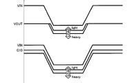
- the figure which shows the 2nd comparative example of a linear power supply The figure which shows the input transient response characteristic of the 2nd comparative example (light load area). The figure which shows the input transient response characteristic of the 2nd comparative example (heavy load area).
- the figure which shows 9th Embodiment of a linear power supply The figure which shows 10th Embodiment of a linear power supply.
- the figure which shows 11th Embodiment of a linear power supply The figure which shows 12th Embodiment of a linear power supply.
- the figure which shows the 13th Embodiment of a linear power supply The figure which shows 14th Embodiment of a linear power supply.
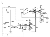
- FIG. 1 is a diagram showing a comparative example of a linear power supply.
- the linear power supply 1 of this comparative example includes an output transistor 10, a voltage dividing unit 20, a driver 30, and a reference voltage adjusting unit 40, and reduces the input voltage VIN to generate a desired output voltage VOUT. ..
- the input voltage VIN is supplied from a battery (not shown) or the like, and its stability is not necessarily high.
- the linear power supply 1 can be used as a reference voltage source with a built-in IC, for example.
- the output transistor 10 is connected between the input end of the input voltage VIN and the output end of the output voltage VOUT, and the conductivity (on-resistance value if the reverse is reversed) is controlled according to the gate signal G10 from the driver 30.
- the gate signal G10 from the driver 30.
- a PMOSFET P-channel type MOSFET
- the output transistor 10 an NMOSFET or a bipolar transistor may be used instead of the PMOSFET.
- the voltage dividing unit 20 includes resistors 21 and 22 (resistance values: R1 and R2) connected in series between the output terminal of the output voltage VOUT and the ground terminal, and outputs the output voltage VOUT from the connection node between both resistors.
- the voltage dividing unit 20 may be omitted and the output voltage VOUT itself may be directly input to the driver 30 as the feedback voltage VFB.
- the driver 30 generates the gate signal G10 so that the feedback voltage VFB input to the non-inverting input terminal (+) matches the predetermined reference voltage VREF input to the inverting input terminal ( ⁇ ) to output the output transistor 10.
- the reference voltage adjusting unit 40 includes an offset applying unit 41, a differential amplifier 42, and a variable voltage source 43 so that the output transistor 10 does not enter the full-on state, in other words, the driver 30 reaches its limit. It has a function of adjusting the reference voltage VREF so that the gate signal G10 is not brought to a low level.
- the offset applying unit 41 offsets the output voltage VOUT to the high potential side by a predetermined offset voltage Voffset.
- the offset voltage Voffset is preferably set to a voltage value lower than the minimum input/output voltage difference VSAT defined by the linear power supply 1 (details will be described later).
- the signal S43 is generated.
- the variable voltage source 43 includes an NMOSFET [N-channel type MOSFET] 43a and a resistor 43b, and adjusts the voltage value of the reference voltage VREF based on the control signal S43 output from the differential amplifier 42.
- the degree of conductivity is controlled based on this. Therefore, the drain current I43a flowing through the NMOSFET 43a increases as the control signal S43 increases and decreases as the control signal S43 decreases.
- the NMOSFET 43a is turned off to keep the reference voltage VREF at a steady value. , The control signal S43 is held at the low level.
- the control signal S43 is increased so that the drain current I43a is passed through the NMOSFET 43a and the reference voltage VREF is decreased from the steady value in order to prevent the decrease. ..
- the configuration that gives the offset to the output voltage VOUT is taken as an example, but conversely, the configuration that gives the offset to the input voltage VIN may be used.
- FIG. 2 is a diagram showing an input transient response characteristic when the reference voltage is fixed.
- the upper part of the figure shows the relationship between the input voltage VIN and the output voltage VOUT, and the middle part of the figure shows the relationship between the reference voltage VREF (dashed line) and the feedback voltage VFB (solid line). ing.
- the lower part of the figure shows the relationship between the input voltage VIN and the gate signal G10.
- the feedback voltage VFB is always the reference voltage VREF. It will be in the state below.
- the driver 30 is in a state in which the gate signal G10 is pulled down to the low level to the limit of its capability, so that the output transistor 10 falls into the full-on state (see times t12 to t15). That is, the driver 30 is in an operation state close to that of the comparator.
- the driver 30 tries to turn off the output transistor 10 by raising the gate signal G10.
- the output voltage VOUT is output as it is while the output transistor 10 remains in the full-on state, and the output voltage VOUT overshoots (see times t15 to t17). If such an overshoot occurs, the load 2 may malfunction or be destroyed.
- the speed at which the output transistor 10 is turned off is determined by the response speed of the driver 30, the current capability of the output stage of the driver 30, the impedance of the internal terminal of the driver 30, or the gate capacitance of the output transistor 10.
- the overshoot convergence time is determined by the characteristics of the driver 30 (phase margin, response speed) and the like.
- FIG. 3 is a diagram showing an input transient response characteristic when the reference voltage is adjusted. Similar to FIG. 2 described above, the upper part of the figure shows the relationship between the input voltage VIN and the output voltage VOUT, and the middle part of the figure shows the reference voltage VREF (dashed line) and the feedback voltage VFB( The relationship with (solid line) is shown. The lower part of the figure shows the relationship between the input voltage VIN and the gate signal G10.
- the reference voltage adjusting unit 40 monitors both the input voltage VIN and the output voltage VOUT, and when the difference voltage (VIN ⁇ VOUT) between them is higher than the offset voltage Voffset, the reference voltage VREF. Is held at a steady value (before time t22 or after time t25), when the difference voltage (VIN-VOUT) is reduced to the offset voltage Voffset, the reference voltage is set so as not to decrease further. The voltage VREF is lowered from the steady value (see times t22 to t25).
- the target value of the output voltage VOUT can always be kept lower than the input voltage VIN even when the input voltage VIN drops. Therefore, the output transistor 10 does not fall into the full-on state, and the driver 30 maintains the gate signal G10 at an appropriate voltage value (for example, VIN-Vth, where Vth is the on-threshold voltage of the output transistor 10).
- the gate signal G10 can be immediately followed by the sudden change and pulled up. Therefore, it is possible to minimize the overshoot of the output voltage VOUT.
- lowering the reference voltage VREF means that the output voltage VOUT is lower than the original target value. Since the decrease in the output voltage VOUT may lead to deterioration in the characteristics of the load 2 connected in the subsequent stage, it is necessary to adjust the reference voltage VREF within a range that does not have such an influence.
- the reference voltage adjusting function described above operates, so that the input voltage VIN It is possible to suppress the overshoot of the output voltage VOUT due to the sudden change of
- the differential voltage (VIN ⁇ VOUT) between the input voltage VIN and the output voltage VOUT Does not fall below the offset voltage Voffset.
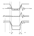
- FIG. 4 is a diagram showing input transient response characteristics in a heavy load region. Similar to FIGS. 2 and 3, the upper part of the figure shows the relationship between the input voltage VIN and the output voltage VOUT, and the middle part of the figure shows the reference voltage VREF (dashed line) and the feedback voltage. The relationship with VFB (solid line) is shown. The lower part of the figure shows the relationship between the input voltage VIN and the gate signal G10.
- the reference voltage adjustment function does not work, and the reference voltage VREF remains held at the steady value. Therefore, when VIN ⁇ Vtarget+ION ⁇ RON is satisfied as the input voltage VIN decreases, the output voltage VOUT cannot be maintained at the output target value Vtarget, and the feedback voltage VFB is always below the reference voltage VREF. As a result, the driver 30 is in a state in which the gate signal G10 is pulled down to the low level to the limit of its capability, so that the output transistor 10 falls into the full-on state (see times t32 to t35).
- the input transient response characteristics in the heavy load region are no different from the input transient response characteristics when the reference voltage is fixed (Fig. 2), and there is no point in introducing the reference voltage adjustment function.
- the simplest solution to solve the above problem is to increase the offset voltage Voffset.
- the offset voltage Voffset is fixedly increased, the output voltage VOUT greatly decreases when the input voltage VIN decreases, regardless of whether the load is light or heavy, which may cause deterioration in characteristics.
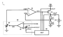
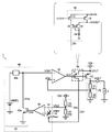
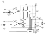
- FIG. 5 is a figure which shows 1st Embodiment of a linear power supply.
- the linear power supply 1 of the present embodiment is based on the comparative example (FIG. 1) described above, and further includes a current detection unit 50.
- the variable voltage source 43 is abbreviated with a single circuit symbol in this figure, its internal configuration is as shown in FIG.
- the current detector 50 detects the output current IOUT flowing through the output transistor 10 and outputs a control signal corresponding to the current value (for example, a sense current corresponding to 1/m of the output current IOUT or a mirror current thereof, details will be described later). ) Is output to the offset giving unit 41.
- the offset applying unit 41 is a circuit block that shifts the output voltage VOUT to the high potential side by the offset voltage Voffset, and newly has a function of variably controlling the offset voltage Voffset according to the control signal from the current detection unit 50. ing.
- the offset voltage Voffset increases as the output current IOUT increases and decreases as the output current IOUT decreases.
- FIGS. 7 and 8 are correlation diagrams of the output current IOUT (horizontal axis) and the output voltage VOUT (vertical axis), respectively.
- 6 shows the output behavior when VREF is fixed
- FIGS. 7 and 8 for comparison reference, the output behavior when VREF is fixed (FIG. 6) is depicted by a broken line.
- the reference voltage adjustment function no longer works. Therefore, the output transistor 10 may be in a full-on state with a decrease in the input voltage VIN, which may cause an overshoot of the output voltage VOUT. If the offset voltage Voffset is increased, the load region in which the reference voltage adjusting function works can be expanded, but as a trade-off, the output decrease at a light load becomes large, as described above.
- the offset voltage Voffset is variably controlled so that the output current IOUT becomes higher and the output current IOUT becomes lower while satisfying IOUT ⁇ RON ⁇ Voffset in all load regions.
- the reference voltage adjustment function described above works regardless of the load conditions. As a result, it is possible to avoid the full-on state of the output transistor 10 in a wide load range, and further suppress the overshoot of the output voltage VOUT in a wide load range to improve the input transient response characteristic of the linear power supply 1. It is possible to raise it.
- FIG. 9 is a diagram showing an input transient response characteristic in the first embodiment (when VREF is adjusted (Voffset variable)).
- the upper part of the figure shows the relationship between the input voltage VIN and the output voltage VOUT, and the lower part of the figure shows the relationship between the input voltage VIN and the gate signal G10.
- the target value of the output voltage VOUT is always kept lower than the input voltage VIN even if the input voltage VIN is lowered by the reference voltage adjustment operation described above. You can Therefore, the output transistor 10 does not fall into the full-on state, and the gate signal G10 is maintained at an appropriate voltage value. Of course, as the load becomes heavier, the gate signal G10 decreases in order to flow more output current IOUT, but the gate signal G10 does not reach the low level to the capacity limit of the driver 30.
- the gate signal G10 can be immediately followed by the sudden change and pulled up. Therefore, it is possible to minimize the overshoot of the output voltage VOUT.
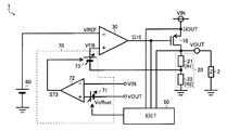
- FIG. 10 is a figure which shows 2nd Embodiment of a linear power supply.
- the linear power supply 1 of the present embodiment is based on the previously described first embodiment (FIG. 5), but is provided with a constant voltage source 60 and a feedback voltage adjustment unit 70 instead of the reference voltage adjustment unit 40.
- the constant voltage source 60 generates a predetermined reference voltage VREF and outputs it to the inverting input terminal ( ⁇ ) of the driver 30.
- the offset applying unit 71 is a circuit block that shifts the output voltage VOUT to the high potential side by the offset voltage Voffset, and, according to the control signal from the current detecting unit 50, as in the first embodiment (FIG. 5). It has a function of variably controlling the offset voltage Voffset. That is, the offset voltage Voffset increases as the output current IOUT increases and decreases as the output current IOUT decreases.
- the signal S73 is generated.
- the variable voltage source 73 adjusts the voltage value of the feedback voltage FB based on the control signal S73 output from the differential amplifier 72. More specifically, the variable voltage source 73 outputs the feedback voltage FB to the non-inverting input terminal (+) of the driver 30 as it is without shifting while the control signal S73 is maintained at a low level, and controls the feedback voltage FB. When the signal S73 rises from the low level, the higher the voltage value, the more the feedback voltage FB shifts to the high potential side.
- the feedback voltage VFB may be adjusted instead of adjusting the reference voltage VREF in order to prevent the output transistor 10 from being fully turned on.
- FIG. 11 is a diagram showing a third embodiment of a linear power supply.
- the linear power supply 1 of the present embodiment is based on the first embodiment (FIG. 5) described above, and further includes a voltage dividing unit 20a that generates the divided input voltage VIN2 from the input voltage VIN.
- the divided input voltage VIN2 is input instead of the input voltage VIN, and the reference voltage VREF is input instead of the output voltage VOUT.
- the circuit elements NMOSFET 43a and resistor 43b
- the variable voltage source 43 depicted as the variable voltage source 43.
- the voltage dividing unit 20a includes resistors 23 and 24 (resistance values: R3 and R4) connected in series between the application terminal of the input voltage VIN and the ground terminal, and the connection node between the two resistors changes the input voltage VIN to the input voltage VIN.
- a PMOSFET 51 is depicted as a specific constituent element of the current detection unit 50.
- the source and gate of the PMOSFET 51 are commonly connected to the source and gate of the output transistor 10, respectively. Therefore, the sense current I51 corresponding to 1/m of the output current IOUT flows through the drain of the PMOSFET 51, and this is output to the offset imparting unit 41 as the control signal described above.
- the sense current I51 is 1/m of the output current IOUT.
- the PMOSFETs 52 and 53 and the currents as the bias means for matching the drain voltage of the PMOSFET 51 with the drain voltage of the output transistor 10 ( output voltage VOUT).
- Source 54 may be added.
- the source of the PMOSFET 52 is connected to the drain of the PMOSFET 51.
- the gates of the PMOSFETs 52 and 53 are both connected to the drain of the PMOSFET 53.
- the drain of the PMOSFET 53 is connected to the first end of the current source 54.
- the second end of the current source 54 is connected to the ground end.
- the drain-source voltage of the PMOSFET 51 can be matched with the drain-source voltage of the output transistor 10. Therefore, it becomes possible to more accurately generate the sense current I51 corresponding to the output current IOUT (and by extension, the control signal to the offset providing unit 41).
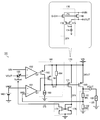
- FIG. 12 is a figure which shows 4th Embodiment of a linear power supply.
- the linear power supply 1 of the present embodiment is based on the previously described third embodiment (FIG. 11), but with some changes.
- NMOSFETs 55 and 56 are added to the current detection unit 50 as current mirrors that generate a mirror current I55 according to the sense current I51.
- the gates of the NMOSFETs 55 and 56 are connected to the drain of the NMOSFET 56.
- the sources of the NMOSFETs 55 and 56 are connected to the ground terminal.
- the drain of the NMOSFET 55 is connected to the offset applying unit 41a as an output end of the mirror current I55.
- the mirror current I55 according to the sense current I51 may be used as the control signal of the offset imparting unit 41a.
- FIG. 13 is a figure which shows 5th Embodiment of a linear power supply.
- the linear power supply 1 of this embodiment is based on the previously described second embodiment (FIG. 10), but with some changes.
- the linear power supply 1 further includes a voltage dividing unit 20a that generates the divided input voltage VIN2 from the input voltage VIN, as in the third embodiment (FIG. 11) and the fourth embodiment (FIG. 12) described above.
- the divided input voltage VIN2 is input instead of the input voltage VIN
- the feedback voltage adjusting section 70 shifts the divided voltage input voltage VIN2 to the lower potential side by the offset voltage Voffset instead of the offset applying section 71 that shifts the output voltage VOUT to the higher potential side by the offset voltage Voffset.
- the variable voltage source 73 also includes a PMOSFET 73a whose conductivity is controlled based on the control signal S73 output from the differential amplifier 72.
- the source of the PMOSFET 73a is connected to the internal power supply having the current capacity necessary for supplying the drain current I73a.
- the feedback voltage FB can be adjusted according to the drain current I73a flowing in the PMOSFET 73a. Specifically, since the PMOSFET 73a is turned off while the control signal S73 is maintained at the high level, the drain current I73a stops flowing. Therefore, the feedback voltage FB is output to the non-inverting input terminal (+) of the driver 30 without being shifted. On the other hand, when the control signal S73 falls from the high level, the lower the voltage value thereof, the higher the conductivity of the PMOSFET 73a, and the larger the drain current I73a flowing through the resistor 22 becomes. Be shifted.
- the current detection unit 50 includes the PMOSFET 51 and the NMOSFETs 55 and 56, and outputs the mirror current I55 described above to the offset imparting unit 71a, as in the fourth embodiment (FIG. 12).
- the mirror current I55 according to the sense current I51 can be used as the control signal of the offset imparting unit 71a.
- FIG. 14 is a figure which shows 6th Embodiment of a linear power supply.
- the linear power supply 1 of the present embodiment is based on the previously described fourth embodiment (FIG. 12) and has a resistor 25 (resistance value: R5) instead of the offset imparting section 41a.
- the resistor 25 is connected between the input terminal of the input voltage VIN and the resistor 23 as a component of the voltage divider 20a.
- the offset voltage Voffset can be generated due to the shift of the resistance ratio due to the insertion of the resistor 25. ..
- FIG. 15 is a figure which shows 7th Embodiment of a linear power supply.
- the linear power supply 1 of this embodiment is based on the previously described fourth embodiment (FIG. 12), but with some changes.
- the reference voltage adjusting unit 40 further includes a resistor 43c (resistance value: R43c) connected between the output end of the reference voltage VREF and the ground end.
- R43c resistance value
- the steady value of the reference voltage VREF may be set by dividing an arbitrary constant voltage (VREF0).
- FIG. 16 is a diagram showing an eighth embodiment of a linear power supply.
- the NMOSFET 43a of the reference voltage adjusting unit 40 is replaced with the PMOSFET 43d while the base of the third embodiment (FIG. 11) described above.
- the source current I43d flowing through the PMOSFET 43d becomes smaller as the control signal S43 is higher, and becomes larger as the control signal S43 is lower.
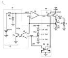
- FIG. 17 is a diagram showing a first comparative example of a linear power supply.
- the linear power supply 101 of the first comparative example includes an output transistor 110, a voltage dividing unit 120, an amplifier 130, and a reference voltage generating unit 140, and lowers the input voltage VIN to generate a desired output voltage VOUT. To do.
- the input voltage VIN is supplied from a battery (not shown) or the like, and its stability is not necessarily high.
- the linear power supply 101 can be used as a reference voltage source with a built-in IC, for example.
- the output transistor 110 is connected between the input terminal of the input voltage VIN and the output terminal of the output voltage VOUT, and the conductivity (on-resistance value if the reverse is reversed) is controlled according to the gate signal G10 from the amplifier 130.
- the gate signal G10 from the amplifier 130.
- a PMOSFET P-channel type MOSFET
- the output transistor 110 an NMOSFET or a bipolar transistor may be used instead of the PMOSFET.
- the voltage dividing unit 120 includes resistors 121 and 122 (resistance values: R1 and R2) connected in series between the output terminal of the output voltage VOUT and the ground terminal, and outputs the output voltage VOUT from a connection node between both resistors.
- the voltage divider 120 may be omitted and the output voltage VOUT itself may be directly input to the amplifier 30 as the feedback voltage VFB.
- the reference voltage generator 140 generates a reference voltage VREF (fixed value) from the input voltage VIN.
- a reference voltage generator 140 for example, a bandgap voltage source having low power supply dependency and temperature dependency can be preferably used.
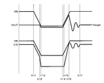
- FIG. 18 is a diagram showing the input transient response characteristic of the first comparative example. The upper part of the figure shows the relationship between the input voltage VIN and the output voltage VOUT, and the lower part of the figure shows the relationship between the input voltage VIN and the gate signal G10.
- the amplifier 130 is in a state in which the gate signal G10 is pulled down to the low level to the limit of its capability, so that the output transistor 110 falls into the full-on state (see times t112 to t115). That is, the amplifier 130 is in an operating state close to that of a comparator.
- the amplifier 130 tries to turn off the output transistor 110 by raising the gate signal G10.
- the input voltage VIN is output as it is while the output transistor 110 is in the full-on state, and the output voltage VOUT overshoots (see times t115 to t117). If such overshoot occurs, the load 102 may malfunction or be destroyed.
- the speed at which the output transistor 110 is turned off is determined by the response speed of the amplifier 130, the current capacity of the output stage of the amplifier 130, the impedance of the internal terminal of the amplifier 130, the gate capacitance of the output transistor 110, and the like.
- the overshoot convergence time is determined by the characteristics of the amplifier 130 (phase margin, response speed) and the like.
- FIG. 19 is a diagram showing a second comparative example of a linear power supply.
- the linear power supply 101 of the second comparative example includes an output transistor 110, a voltage dividing unit 120, amplifiers 131 and 132, a reference voltage generating unit 140, an offset applying unit 150, and a gate driving unit 160,
- the input voltage VIN is stepped down to generate a desired output voltage VOUT. It should be noted that the same reference numerals as those in FIG.
- the amplifier 131 forms a first output feedback loop for matching the feedback voltage VFB with the reference voltage VREF.
- the offset applying unit 150 is a circuit block that applies a predetermined offset voltage Voffset to the amplifier 132. More specifically, for example, the offset applying unit 150 shifts the output voltage VOUT to the high potential side by a predetermined offset voltage Voffset and then outputs it to the inverting input terminal ( ⁇ ) of the amplifier 132.
- the offset voltage Voffset is preferably set to a voltage value lower than the minimum input/output voltage difference VSAT defined by the linear power supply 101 (details will be described later).
- the gate driver 160 receives the gate signals G1 and G2 in the same row as two-system output feedback signals without directly connecting the output end of the amplifier 131 to the gate of the output transistor 110, and according to the gate signals G1 and G2, It is a circuit block that generates the gate signal G10 of the output transistor 110, and includes PMOSFETs 161 and 162, a current source 163, and a resistor 164.
- the source of the PMOSFET 161 is connected to the input terminal of the input voltage VIN.
- the drain of the PMOSFET 161 is connected to the gate of the output transistor 110.
- the source of the PMOSFET 162 is connected to the input terminal of the input voltage VIN.
- the drain of the PMOSFET 162 is connected to the gate of the output transistor 110.
- the current source 163 is connected between the gate of the output transistor 110 and the ground terminal, and generates a predetermined constant current.
- the resistor 164 is a high resistance (for example, several M ⁇ ) connected between the input terminal of the input voltage VIN and the gate of the output transistor 110.
- FIG. 20 is a diagram showing the input transient response characteristic of the second comparative example (light load region). Similar to FIG. 18, the upper part of the figure shows the relationship between the input voltage VIN and the output voltage VOUT, and the lower part of the figure shows the relationship between the input voltage VIN and the gate signal G10. Has been done.
- the gate signal G10 of the output transistor 110 changes following the input voltage VIN while maintaining a constant potential difference with respect to the input voltage VIN. That is, since the gate signal G10 does not stick to the low level, the output transistor 110 does not fall into the full-on state.
- the gate signal G10 can immediately follow the sudden change and can be pulled up. Therefore, it is possible to minimize the overshoot of the output voltage VOUT.
- the decrease in the output voltage VOUT may lead to deterioration of the characteristics of the load 102 connected in the subsequent stage, so it is necessary to adjust the offset voltage Voffset within a range that does not have such an influence.
- the output feedback control by the amplifier 132 works effectively. It is possible to suppress the overshoot of the output voltage VOUT due to the sudden change of the voltage VIN.
- the differential voltage (VIN ⁇ VOUT) between the input voltage VIN and the output voltage VOUT Does not fall below the offset voltage Voffset.
- the gate signal G2 is always at the high level, the PMOSFET 162 remains off and the output feedback control by the amplifier 132 does not work.
- FIG. 21 is a diagram showing an input transient response characteristic of the second comparative example (heavy load region). Similar to FIGS. 18 and 20, the upper part of the figure shows the relationship between the input voltage VIN and the output voltage VOUT, and the lower part of the figure shows the relationship between the input voltage VIN and the gate signal G10. Relationships are shown.
- the output feedback control by the amplifier 132 does not work in the heavy load area. Therefore, when VIN ⁇ Vtarget+ION ⁇ RON is satisfied as the input voltage VIN decreases, the output voltage VOUT cannot be maintained at the output target value Vtarget, and the feedback voltage VFB is always below the reference voltage VREF. As a result, the amplifier 131 enters a state in which the gate signal G1 is pulled up to a high level, and the PMOSFET 161 is also turned off. As a result, the gate signal G10 is brought to a low level by the current source 163, so that the output transistor 110 falls into the full-on state (see times t132 to t135).
- the amplifier 131 pulls down the gate signal G1 to increase the conductivity of the PMOSFET 161, thereby pulling up the gate signal G10 and turning off the output transistor 110. try to.
- the input voltage VIN is output as it is while the output transistor 110 is in the full-on state, and the output voltage VOUT overshoots (see times t135 to t137).
- the input transient response characteristic (Fig. 21) in the heavy load region is no different from the input transient response characteristic of the first comparative example (Fig. 18).
- the simplest solution to solve the above problem is to increase the offset voltage Voffset.
- the offset voltage Voffset is fixedly increased, the output voltage VOUT greatly decreases when the input voltage VIN decreases, regardless of whether the load is light or heavy, which may cause deterioration in characteristics.
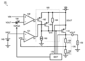
- FIG. 22 is a figure which shows 9th Embodiment of a linear power supply.
- the linear power supply 101 of the present embodiment is based on the previously described second comparative example (FIG. 19), and further includes a current detection unit 170.
- the current detector 170 detects the output current IOUT flowing through the output transistor 110, and outputs a control signal corresponding to the current value (for example, a sense current corresponding to 1/m of the output current IOUT or a mirror current thereof, details will be described later). ) Is output to the offset giving unit 150.
- the offset providing unit 150 is a circuit block that shifts the output voltage VOUT to the high potential side by the offset voltage Voffset, and newly has a function of variably controlling the offset voltage Voffset according to the control signal from the current detection unit 170. ing.
- the offset voltage Voffset increases as the output current IOUT increases and decreases as the output current IOUT decreases.
- FIGS. 6 to 8 are the correlation diagrams of the output current IOUT (horizontal axis) and the output voltage VOUT (vertical axis), respectively.
- 6 can be understood as showing the output behavior of the first comparative example
- FIG. 7 can be understood as showing the output behavior of the second comparative example (fixed Voffset).
- FIG. 8 can be understood as showing the output behavior of the ninth embodiment (variable Voffset).
- FIGS. 7 and 8 the output behavior of the first comparative example (FIG. 6) is depicted by a broken line for comparison reference. Below, the superiority of the ninth embodiment will be described while comparing the drawings.
- the output behavior of FIG. 6 (first comparative example) will be described.
- the amplifier 132 no longer works effectively. Therefore, as the input voltage VIN decreases, the output transistor 110 may be in a full-on state, which may cause overshoot of the output voltage VOUT. If the offset voltage Voffset is increased, the load region in which the amplifier 132 works effectively can be expanded, but as a trade-off, the output decrease at a light load becomes large, as described above.
- the offset voltage Voffset is variably controlled so that the output current IOUT becomes higher and the output current IOUT becomes lower while satisfying IOUT ⁇ RON ⁇ Voffset in all load regions.
- FIG. 9 described above can be understood as a diagram showing an input transient response characteristic of the ninth embodiment (variable Voffset).
- the upper part of the figure shows the relationship between the input voltage VIN and the output voltage VOUT, and the lower part of the figure shows the relationship between the input voltage VIN and the gate signal G10.
- the voltage can be maintained at Voffset. Therefore, the output transistor 110 does not fall into the full-on state, and the gate signal G10 is maintained at an appropriate voltage value.
- the gate signal G10 lowers because more output current IOUT flows, but the state is not lowered to the ground level.
- the gate signal G10 of the output transistor 110 changes following the input voltage VIN while maintaining a constant potential difference with respect to the input voltage VIN. That is, since the gate signal G10 does not stick to the low level, the output transistor 110 does not fall into the full-on state.
- the gate signal G10 can immediately follow the sudden change and can be pulled up. Therefore, it is possible to minimize the overshoot of the output voltage VOUT.
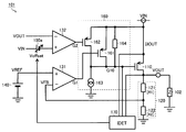
- FIG. 23 is a diagram showing a tenth embodiment of a linear power supply.
- the linear power supply 101 of the present embodiment is based on the ninth embodiment (FIG. 22) described above, but instead of the offset giving unit 150 that gives an offset to the output voltage VOUT, an offset giving unit that gives an offset to the input voltage VIN. 150a is provided.
- the offset applying unit 150a shifts the input voltage VIN to the low potential side by the offset voltage Voffset, and then outputs it to the non-inverting input terminal (+) of the amplifier 132. Further, the offset applying unit 150a has a function of variably controlling the offset voltage Voffset in accordance with the control signal from the current detecting unit 170, as in the previous ninth embodiment (FIG. 22). That is, the offset voltage Voffset increases as the output current IOUT increases and decreases as the output current IOUT decreases.
- Output feedback control is applied so as to make an imaginary short circuit.
- the gate signal G10 of the output transistor 110 changes following the input voltage VIN while maintaining a constant potential difference with respect to the input voltage VIN. That is, since the gate signal G10 does not stick to the low level, the output transistor 110 does not fall into the full-on state.
- the offset voltage Voffset may be subtracted from the input voltage VIN instead of being added to the output voltage VOUT.
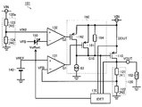
- FIG. 24 is a figure which shows 11th Embodiment of a linear power supply.
- the linear power supply 101 of the present embodiment is based on the ninth embodiment (FIG. 22) described above, and further includes a voltage dividing unit 120a that generates the divided input voltage VIN2 from the input voltage VIN.
- the voltage input to the inverting input terminal ( ⁇ ) of the amplifier 132 is not limited to the feedback voltage FB, but may be any voltage that behaves similarly to the output voltage VOUT.
- the output voltage VOUT may be divided at a division ratio different from that of the voltage dividing unit 120, and the divided output voltage may be input to the inverting input terminal ( ⁇ ) of the amplifier 132.
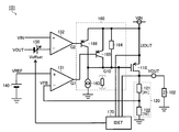
- FIG. 25 is a figure which shows 12th Embodiment of a linear power supply.
- the linear power supply 101 of this embodiment is based on the previously described ninth embodiment (FIG. 22), but the configuration of the gate drive section 160 is modified. More specifically, the gate driver 160 includes pnp-type bipolar transistors 165 and 166 instead of the PMOSFETs 161 and 162.
- the emitters of the transistors 165 and 166 are connected to the input terminal of the input voltage VIN.
- the collectors of the transistors 165 and 166 are connected to the gate of the output transistor 110.
- the bases of the transistors 165 and 166 are connected to the output terminals of the amplifiers 131 and 132, respectively.
- the PMOSFETs 161 and 162 can be replaced with the pnp-type bipolar transistors 165 and 166.
- the gate signals G1 and G2 may be understood as base signals.
- the current source 163 that generates the drive current of the gate drive unit 160 may be replaced by a resistor or the like as shown in the parentheses in this figure.
- FIG. 26 is a figure which shows 13th Embodiment of a linear power supply.
- the linear power supply 101 of this embodiment is based on the previously described ninth embodiment (FIG. 22), but the configuration of the gate drive section 160 is modified. More specifically, the gate driver 160 includes NMOSFETs 167 and 168 and a current source 169 instead of the PMOSFETs 161 and 162 and the current source 163.
- the first end of the current source 169 is connected to the input end of the input voltage VIN.
- the second end of the current source 169 and the drain of the NMOSFET 168 are connected to the gate of the output transistor 110.
- the source of the NMOSFET 168 is connected to the drain of the NMOSFET 167.
- the source of the NMOSFET 167 is connected to the ground terminal.
- the gates of the NMOSFETs 167 and 168 are connected to the output terminals of the amplifiers 131 and 132, respectively.
- the output terminals of the amplifiers 131 and 132 are logically connected in series as shown in this figure.
- the output form of each of the amplifiers 131 and 132 (each output) Whether the ends are logically connected in parallel or connected in series) must be used properly.
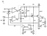
- FIG. 27 is a figure which shows 14th Embodiment of a linear power supply.
- the source and gate of the PMOSFET 171 are connected to the source and gate of the output transistor 110, respectively. Therefore, the sense current I71 corresponding to the output current IOUT flows through the drain of the PMOSFET 171.
- the size ratio between the output transistor 110 and the PMOSFET 171 is m:1 (where m>1)
- the sense current I71 is 1/m of the output current IOUT.
- Source 174 may be added.
- the source of the PMOSFET 172 is connected to the drain of the PMOSFET 171.
- the gates of the PMOSFETs 172 and 173 are both connected to the drain of the PMOSFET 173.
- the drain of the PMOSFET 173 is connected to the first end of the current source 174.
- the second end of the current source 174 is connected to the ground end.
- the drain-source voltage of the PMOSFET 171 can be matched with the drain-source voltage of the output transistor 110. Therefore, it becomes possible to more accurately generate the sense current I71 according to the output current IOUT (and by extension, the control signal to the offset imparting unit 150).
- NMOSFETs 175 and 176 are provided as mirrors.
- the gates of the NMOSFETs 175 and 176 are connected to the drain of the NMOSFET 176.
- the sources of the NMOSFETs 175 and 176 are connected to the ground terminal.
- the drain of the NMOSFET 175 is connected to the offset applying unit 150 as an output end of the control current I75.
- FIG. 28 is a figure which shows 15th Embodiment of a linear power supply.
- the linear power supply 101 of the present embodiment is based on the previous 14th embodiment (FIG. 27), but the configuration of the current detection unit 170 is modified. More specifically, the current detector 170 includes an NMOSFET 177, an amplifier 178, and resistors 179 and 17A (resistance values Rx and Ry) instead of the NMOSFETs 175 and 176.
- the non-inverting input terminal (+) of the amplifier 178 and the first terminal of the resistor 179 are connected to the drain of the PMOSFET 171.
- the inverting input terminal ( ⁇ ) of the amplifier 178 and the first terminal of the resistor 17A are connected to the source of the NMOSFET 177.
- the second end of each of the resistors 179 and 17A is connected to the ground end.
- the output terminal of the amplifier 178 is connected to the gate of the NMOSFET 177.
- the drain of the NMOSFET 177 is connected to the offset giving unit 150 as an output end of the control current I77.
- the means for generating the control signal (control current) according to the sense current I71 is not limited to the current mirror.
- the linear power supply disclosed in this specification is such that an output transistor connected between an input terminal of an input voltage and an output terminal of an output voltage and a feedback voltage corresponding to the output voltage match a reference voltage.
- a driver for driving the output transistor a current detector for detecting an output current flowing through the output transistor, a first voltage according to the input voltage, and a second voltage according to the output voltage or the reference voltage.
- the voltage adjusting unit adjusts the reference voltage or the feedback voltage so that the differential voltage does not fall below the offset voltage according to the output current (first configuration).
- the first voltage may be the input voltage itself or a divided voltage of the input voltage.
- the output current is IOUT
- the ON resistance value of the output transistor in the full-ON state is RON
- the offset voltage is Voffset
- the offset voltage is in all load regions. It is advisable to adopt a configuration (second configuration) that is variably controlled so as to satisfy IOUT ⁇ RON ⁇ Voffset.
- the offset voltage is set to a voltage value lower than a minimum input-output voltage difference defined by the linear power supply (third configuration). ) Is recommended.
- the voltage adjustment unit holds the reference voltage at a steady value when the differential voltage is higher than the offset voltage, while the differential voltage is It is preferable that the reference voltage is reduced from the steady value (fourth configuration) so that the differential voltage is not further reduced when the offset voltage is reduced.
- the voltage adjusting section transmits the feedback voltage as it is to the driver when the differential voltage is higher than the offset voltage, while the differential voltage is A configuration (fifth configuration) may be adopted in which the feedback voltage is raised and transmitted to the driver so that the differential voltage is not further reduced when the offset voltage is reduced.
- the voltage adjusting unit includes an offset applying unit that shifts the second voltage to a high potential side by the offset voltage, and the first voltage and the offset. And a variable voltage source that adjusts the reference voltage or the feedback voltage based on the output signal of the differential amplifier (sixth configuration) ) Is recommended.
- the voltage adjusting unit includes an offset applying unit that shifts the first voltage to a lower potential side by the offset voltage, and the second voltage and the offset.
- a configuration including a differential amplifier to which the completed first voltage is differentially input, and a variable voltage source that adjusts the reference voltage or the feedback voltage based on an output signal of the differential amplifier (seventh configuration) ).
- the variable voltage source includes a transistor whose conductivity is controlled based on an output signal of the differential amplifier, and the variable voltage source is configured to operate in accordance with a current flowing through the transistor.
- a configuration (eighth configuration) for adjusting the reference voltage or the feedback voltage is preferable.
- the linear power supply having any one of the first to eighth configurations is connected in series between the output voltage application terminal and the ground terminal, and outputs the feedback voltage from a mutual connection node. Further comprising a second resistor, a third resistor and a fourth resistor connected in series between the input voltage application terminal and the ground terminal and outputting the first voltage from a connection node between them.
- the resistance value of one resistor is R1
- the resistance value of the second resistor is R2
- the resistance value of the third resistor is R3
- the resistance value of the fourth resistor is R4
- R1:R2 R3:R4
- the linear power supply having a seventh configuration includes a first resistor and a second resistor that are connected in series between the output voltage application terminal and a ground terminal and output the feedback voltage from a connection node between them.
- a third resistor and a fourth resistor connected in series between the input terminal of the input voltage and a ground terminal to output the first voltage from a connection node between them, the input terminal of the input voltage and the first resistor
- a resistance value of the first resistance is R1
- a resistance value of the second resistance is R2
- a resistance value of the third resistance is R3, and a fifth resistance connected between
- (10th configuration) is preferable.
- the linear power supply disclosed in this specification includes an output transistor connected between an input end of an input voltage and an output end of an output voltage, the output voltage or a voltage corresponding thereto and a predetermined reference.
- a first amplifier that amplifies a difference from a voltage to generate a first drive signal; and a second drive signal that amplifies a difference between the input voltage or a voltage corresponding thereto and the output voltage or a voltage corresponding thereto
- a second amplifier that generates a control signal, a drive unit that drives the output transistor according to the first and second drive signals, and a current detection unit that detects an output current flowing through the output transistor and generates a control signal.
- An offset imparting unit that imparts an offset voltage according to the control signal to the second amplifier is provided (eleventh configuration).
- the output current is IOUT
- the on-resistance value of the output transistor in a full-on state is RON
- the offset voltage is Voffset
- the offset voltage is in all load regions. It is advisable to adopt a configuration (twelfth configuration) that is variably controlled so as to satisfy IOUT ⁇ RON ⁇ Voffset.
- the offset voltage is set to a voltage value lower than a minimum input-output voltage difference defined by the linear power supply (thirteenth configuration).
- the offset applying unit shifts the output voltage or a voltage corresponding to the output voltage to a high potential side by the offset voltage and then the second A configuration (14th configuration) for outputting to the amplifier is preferable.
- the offset applying unit shifts the input voltage or a voltage corresponding to the input voltage to a low potential side by the offset voltage and then the second voltage is applied. It may be configured to output to the amplifier (fifteenth configuration).
- the linear power supply having any one of the eleventh to fifteenth configurations is connected in series between the output terminal of the output voltage and the ground terminal, and divides the voltage from the mutual connection node toward the second amplifier.
- the first and second resistors that output an output voltage, and the input terminal of the input voltage and the ground terminal are connected in series, and the divided input voltage is output from the mutual connection node toward the second amplifier.
- a configuration further including a third and a fourth resistor, wherein R1:R2 R3:R4 is satisfied, where the resistance values of the first to fourth resistors are R1, R2, R3, and R4 (sixteenth configuration ) Is recommended.
- the drive unit is connected in parallel between the input end of the input voltage and the control end of the output transistor, and respectively connected to the first and the first ends.
- a structure including the first and second transistors driven by the second drive signal (seventeenth structure) is preferable.
- the driving unit is connected in series between a control end of the output transistor and a grounding end, and is connected to the first and second driving signals, respectively.
- a configuration including the first and second transistors driven by (18th configuration) is also preferable.
- the current detection unit includes a sense transistor that generates a sense current according to the output current, and the sense current or a current corresponding thereto.
- a signal may be output as the control signal to the offset imparting unit (19th configuration).
- the current detection unit further includes a bias unit that matches output node voltages of the sense transistor and the output transistor (twentieth configuration).
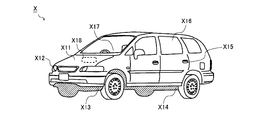
- FIG. 29 is an external view of the vehicle X.
- the vehicle X of this configuration example is equipped with various electronic devices X11 to X18 that operate by receiving supply of power supply voltage from a battery (not shown).
- the mounting positions of the electronic devices X11 to X18 in this figure may be different from the actual positions for convenience of illustration.
- the electronic device X11 is an engine control unit that performs control related to the engine (injection control, electronic throttle control, idling control, oxygen sensor heater control, auto cruise control, etc.).
- the electronic device X12 is a lamp control unit that controls lighting such as HID [high intensity discharged lamp] and DRL [daytime running lamp].
- the electronic device X13 is a transmission control unit that performs control related to the transmission.
- the electronic device X14 is a braking unit that performs control related to the movement of the vehicle X (ABS [anti-lock brake system] control, EPS [electric power steering] control, electronic suspension control, etc.).
- ABS anti-lock brake system
- EPS electric power steering
- electronic suspension control etc.
- the electronic device X15 is a security control unit that controls the driving of door locks and crime prevention alarms.
- the electronic device X16 is a standard equipment item or a manufacturer option item such as a wiper, an electric door mirror, a power window, a damper (shock absorber), an electric sunroof, and an electric seat, which are incorporated in the vehicle X at the factory shipment stage. Is.
- the electronic device X17 is an electronic device such as an in-vehicle A/V [audio/visual] device, a car navigation system, and an ETC [electronic toll collection system] that is optionally attached to the vehicle X as a user option item.
- the electronic device X18 is an electronic device equipped with a high withstand voltage motor such as an in-vehicle blower, an oil pump, a water pump, and a battery cooling fan.
- a high withstand voltage motor such as an in-vehicle blower, an oil pump, a water pump, and a battery cooling fan.
- the linear power supply 1 described above can be incorporated into any of the electronic devices X11 to X18.
- the invention disclosed in this specification can be used for vehicle-related equipment, ship-related equipment, office equipment, portable equipment, or smartphones.
Landscapes
- Engineering & Computer Science (AREA)
- Physics & Mathematics (AREA)
- Electromagnetism (AREA)
- General Physics & Mathematics (AREA)
- Radar, Positioning & Navigation (AREA)
- Automation & Control Theory (AREA)
- Microelectronics & Electronic Packaging (AREA)
- Nonlinear Science (AREA)
- Continuous-Control Power Sources That Use Transistors (AREA)
Abstract
リニア電源1は、入力電圧VINの入力端と出力電圧VOUTの出力端との間に接続された出力トランジスタ10と、出力電圧VOUTに応じた帰還電圧VFBが基準電圧VREFと一致するように出力トランジスタ10を駆動するドライバ30と、出力トランジスタ10に流れる出力電流IOUTを検出する電流検出部50と、入力電圧VINに応じた第1電圧(例えばVIN自体)と出力電圧VOUTまたは基準電圧VREFに応じた第2電圧(例えばVOUT自体)との差分電圧が出力電流IOUTに応じたオフセット電圧Voffsetを下回らないように基準電圧VREFまたは帰還電圧VFBを調整する電圧調整部40と、を有する。
Description
本明細書中に開示されている発明は、リニア電源に関する。
従来より、様々なデバイスの電源手段として、リニア電源(=LDO[low drop out]レギュレータなどのシリーズレギュレータ)が用いられている。
ところで、安定度の低い入力電圧(例えばバッテリ電圧)の供給を受けるリニア電源では、入力電圧の過渡的な変動に対する応答特性(=入力過渡応答特性)を高めておく必要がある。なぜなら、入力過渡応答特性が低いと、入力電圧の変動時に出力電圧まで変動してしまい、負荷の特性悪化や破壊などの原因となり得るからである。特に、近年では、リニア電源に供給される入力電圧の低電圧化が進んでおり、入力過渡応答特性に対する要求も厳しくなっている。
なお、本願出願人は、これまでにも入力過渡応答特性の高いリニア電源(特許文献1ないしは特許文献2)を提案しているが、幅広い負荷領域での使用を鑑みると、更なる改善の余地があった。
本明細書中に開示されている発明は、本願の発明者により見出された上記課題に鑑み、幅広い負荷領域で入力過渡応答特性の高いリニア電源を提供することを目的とする。
本明細書中に開示されているリニア電源は、入力電圧の入力端と出力電圧の出力端との間に接続された出力トランジスタと、前記出力電圧に応じた帰還電圧が基準電圧と一致するように前記出力トランジスタを駆動するドライバと、前記出力トランジスタに流れる出力電流を検出する電流検出部と、前記入力電圧に応じた第1電圧と前記出力電圧または前記基準電圧に応じた第2電圧との差分電圧が前記出力電流に応じたオフセット電圧を下回らないように前記基準電圧または前記帰還電圧を調整する電圧調整部とを有する。
また、本明細書中に開示されているリニア電源は、入力電圧の入力端と出力電圧の出力端との間に接続された出力トランジスタと、前記出力電圧またはこれに応じた電圧と所定の基準電圧との差分を増幅して第1駆動信号を生成する第1アンプと、前記入力電圧またはこれに応じた電圧と前記出力電圧またはこれに応じた電圧との差分を増幅して第2駆動信号を生成する第2アンプと、前記第1及び第2駆動信号に応じて前記出力トランジスタを駆動する駆動部と、前記出力トランジスタに流れる出力電流を検出して制御信号を生成する電流検出部と、前記制御信号に応じたオフセット電圧を前記第2アンプに与えるオフセット付与部と、を有する。
なお、本発明のその他の特徴、要素、ステップ、利点、及び、特性については、以下に続く実施形態の詳細な説明やこれに関する添付の図面によって、さらに明らかとなる。
本明細書中に開示されている発明によれば、幅広い負荷領域で入力過渡応答特性の高いリニア電源を提供することが可能となる。
<比較例>
まず、リニア電源に関する新規な実施形態(第1~第8実施形態)の説明に先立ち、それらと対比される比較例について簡単に説明しておく。図1は、リニア電源の比較例を示す図である。本比較例のリニア電源1は、出力トランジスタ10と、分圧部20と、ドライバ30と、基準電圧調整部40と、を有し、入力電圧VINを降圧して所望の出力電圧VOUTを生成する。入力電圧VINは、不図示のバッテリなどから供給されており、その安定度は必ずしも高くない。出力電圧VOUTは、後段の負荷2(=二次電源やマイコンなど)に供給されている。リニア電源1は、例えば、IC内蔵の基準電圧源として用いることができる。
まず、リニア電源に関する新規な実施形態(第1~第8実施形態)の説明に先立ち、それらと対比される比較例について簡単に説明しておく。図1は、リニア電源の比較例を示す図である。本比較例のリニア電源1は、出力トランジスタ10と、分圧部20と、ドライバ30と、基準電圧調整部40と、を有し、入力電圧VINを降圧して所望の出力電圧VOUTを生成する。入力電圧VINは、不図示のバッテリなどから供給されており、その安定度は必ずしも高くない。出力電圧VOUTは、後段の負荷2(=二次電源やマイコンなど)に供給されている。リニア電源1は、例えば、IC内蔵の基準電圧源として用いることができる。
出力トランジスタ10は、入力電圧VINの入力端と出力電圧VOUTの出力端との間に接続されており、ドライバ30からのゲート信号G10に応じて導通度(裏を返せばオン抵抗値)が制御される。なお、本図の例では、出力トランジスタ10として、PMOSFET[P-channel type MOSFET]が用いられている。従って、ゲート信号G10が低いほど、出力トランジスタ10の導通度が高くなり、出力電圧VOUTが上昇する。逆に、ゲート信号G10が高いほど、出力トランジスタ10の導通度が低くなり、出力電圧VOUTが低下する。ただし、出力トランジスタ10としては、PMOSFETに代えて、NMOSFETを用いてもよいし、バイポーラトランジスタを用いてもよい。
分圧部20は、出力電圧VOUTの出力端と接地端との間に直列接続された抵抗21及び22(抵抗値:R1及びR2)を含み、両抵抗相互間の接続ノードから出力電圧VOUTに応じた帰還電圧VFB(=VOUT×{R2/(R1+R2)})を出力する。ただし、出力電圧VOUTがドライバ30の入力ダイナミックレンジに収まっていれば、分圧部20を割愛し、帰還電圧VFBとして出力電圧VOUTそのものをドライバ30に直接入力しても構わない。
ドライバ30は、非反転入力端(+)に入力される帰還電圧VFBが反転入力端(-)に入力される所定の基準電圧VREFと一致するようにゲート信号G10を生成して出力トランジスタ10を駆動する。より具体的に述べると、ドライバ30は、帰還電圧VFBと基準電圧VREFとの差分値ΔV(=VFB-VREF)が高いほどゲート信号G10を引き上げ、逆に、差分値ΔVが低いほどゲート信号G10を引き下げる。
基準電圧調整部40は、オフセット付与部41と、差動アンプ42と、可変電圧源43と、を含み、出力トランジスタ10がフルオン状態とならないように、言い換えれば、ドライバ30がその能力の限界までゲート信号G10をローレベルに引き下げた状態とならないように、基準電圧VREFを調整する機能を備えている。
オフセット付与部41は、出力電圧VOUTを所定のオフセット電圧Voffset分だけ高電位側にオフセットさせる。なお、オフセット電圧Voffsetは、リニア電源1で規定されている最低入出力間電圧差VSATよりも低い電圧値に設定することが望ましい(詳細は後述)。
差動アンプ42では、反転入力端(-)に入力される入力電圧VINと、非反転入力端(+)に入力されるオフセット済みの出力電圧(=VOUT+Voffset)に応じて可変電圧源43の制御信号S43が生成される。
可変電圧源43は、NMOSFET[N-channel type MOSFET]43aと抵抗43bを含み、差動アンプ42から出力される制御信号S43に基づいて基準電圧VREFの電圧値を調整する。
NMOSFET43aは、ドライバ30の反転入力端(-)(=基準電圧VREFの出力端)と接地端との間に接続されており、差動アンプ42から出力される制御信号S43(=ゲート信号)に基づいて導通度が制御される。従って、NMOSFET43aに流れるドレイン電流I43aは、制御信号S43が高いほど大きくなり、制御信号S43が低いほど小さくなる。
抵抗43b(抵抗値:R43b)は、基準電圧VREF0(=基準電圧VREFの定常値に相当)の印加端とドライバ30の反転入力端(-)との間に接続されており、NMOSFET43aに流れるドレイン電流I43aを受けて自身の両端間に生じる電圧降下分(=I43a×R43b)だけ基準電圧VREF0を引き下げることにより、基準電圧VREF(=VREF0-I43a×R43b)を生成する。すなわち、基準電圧VREFは、I43a=0Aであるときに定常値(=VREF0)となり、ドレイン電流I43aが大きくなるほど定常値から低下していく。
本実施形態のリニア電源1において、入力電圧VINと出力電圧VOUTとの差分電圧(VIN-VOUT)がオフセット電圧Voffsetよりも高いときには、NMOSFET43aをオフして基準電圧VREFを定常値に保持するように、制御信号S43がローレベルに保持される。
一方、差分電圧(VIN-VOUT)がオフセット電圧Voffsetまで低下したときには、そのさらなる低下を防止すべく、NMOSFET43aにドレイン電流I43aを流して基準電圧VREFを定常値から引き下げるように制御信号S43が高められる。
なお、上記では、出力電圧VOUTにオフセットを与える構成を例に挙げたが、逆に、入力電圧VINにオフセットを与える構成としても構わない。具体的には、本図中の括弧内で示したように、入力電圧VINをオフセット電圧Voffset分だけ低電位側にオフセットさせるオフセット付与部を設け、出力電圧VOUTとオフセット済みの入力電圧(=VIN-Voffset)を差動アンプ42に差動入力してもよい。
<入力過渡応答特性(基準電圧固定時)>
上記した基準電圧調整機能の導入意義を説明するに先立ち、基準電圧VREFが固定値である場合の入力過渡応答特性について簡単に説明する。
上記した基準電圧調整機能の導入意義を説明するに先立ち、基準電圧VREFが固定値である場合の入力過渡応答特性について簡単に説明する。
図2は、基準電圧固定時の入力過渡応答特性を示す図である。なお、本図上段には、入力電圧VINと出力電圧VOUTとの関係が示されており、本図中段には、基準電圧VREF(一点鎖線)と帰還電圧VFB(実線)との関係が示されている。また、本図下段には、入力電圧VINとゲート信号G10との関係が示されている。
仮に、基準電圧VREFが固定値である場合、入力電圧VINの低下に伴い、入力電圧VINが出力目標値Vtarget(=出力電圧VOUTの目標値)よりも低くなると、帰還電圧VFBが常に基準電圧VREFを下回った状態となる。その結果、ドライバ30は、その能力の限界までゲート信号G10をローレベルに引き下げた状態となるので、出力トランジスタ10がフルオン状態に陥る(時刻t12~t15を参照)。すなわち、ドライバ30がコンパレータに近い動作状態となる。
このような状態から入力電圧VINが出力目標値Vtargetよりも高い電圧まで急上昇した場合、ドライバ30は、ゲート信号G10を引き上げて出力トランジスタ10をオフしようとする。しかしながら、ローレベルに振り切れた状態のゲート信号G10を、入力電圧VINの急変に即時追従させて引き上げることは難しい。その結果、出力トランジスタ10がフルオン状態とされたまま、入力電圧VINをそのまま出力してしまい、出力電圧VOUTのオーバーシュートを生じる(時刻t15~t17を参照)。このようなオーバーシュートが生じると、負荷2が誤動作したり破壊に至るおそれがある。
なお、出力トランジスタ10をオフさせるスピードは、ドライバ30の応答速度、ドライバ30の出力段における電流能力、ドライバ30の内部端子が持つインピーダンス、ないしは、出力トランジスタ10のゲート容量などによって決まる。また、オーバーシュートの収束時間は、ドライバ30の特性(位相余裕度、応答速度)などによって決まる。
<入力過渡応答特性(基準電圧調整時)>
次に、基準電圧VREFが可変値である場合の入力過渡応答特性について説明する。
次に、基準電圧VREFが可変値である場合の入力過渡応答特性について説明する。
図3は、基準電圧調整時の入力過渡応答特性を示す図である。なお、先出の図2と同じく、本図上段には、入力電圧VINと出力電圧VOUTとの関係が示されており、本図中段には、基準電圧VREF(一点鎖線)と帰還電圧VFB(実線)との関係が示されている。また、本図下段には、入力電圧VINとゲート信号G10との関係が示されている。
本比較例のリニア電源1において、基準電圧調整部40は、入力電圧VINと出力電圧VOUTの双方を監視し、両者の差分電圧(VIN-VOUT)がオフセット電圧Voffsetよりも高いときには、基準電圧VREFを定常値に保持する一方(時刻t22以前、若しくは、時刻t25以降を参照)、上記の差分電圧(VIN-VOUT)がオフセット電圧Voffsetまで低下したときには、これが更に低下してしまわないように、基準電圧VREFを定常値から引き下げる(時刻t22~t25を参照)。
上記の基準電圧調整動作により、入力電圧VINが低下した場合でも、出力電圧VOUTの目標値を入力電圧VINよりも常に低い状態に維持することができる。従って、出力トランジスタ10がフルオン状態に陥ることはなく、ドライバ30は、ゲート信号G10を適切な電圧値(例えばVIN-Vth、ただしVthは出力トランジスタ10のオンスレッショルド電圧)に維持した状態となる。
このように、入力電圧VINの低下に伴う出力トランジスタ10のフルオン状態を回避しておけば、その後、入力電圧VINが急上昇したとしても、その急変にゲート信号G10を即時追従させて引き上げることができるので、出力電圧VOUTのオーバーシュートを最小限に抑制することが可能となる。
なお、基準電圧VREFを引き下げるということは、出力電圧VOUTが本来の目標値よりも低下することを意味する。出力電圧VOUTの低下は、後段に接続される負荷2の特性悪化に繋がるおそれがあるので、そのような影響を及ぼさない範囲で基準電圧VREFを調整する必要がある。
一つの目安として、リニア電源1で規定されている最低入出力間電圧差VSATに着目する。最低入出力間電圧差VSATとは、リニア電源1から負荷2に所定の出力電流IOUTを安定供給するために最低限必要な入出力間電圧差(=入力電圧VINと出力電圧VOUTとの差分電圧(VIN-VOUT))に相当し、一般には、出力トランジスタ10のフルオン状態におけるオン抵抗値RONと、そのときに流れる出力電流IOUTの電流値に応じて決まる。
これを鑑みると、オフセット電圧Voffset(=入力電圧VINの低下時における出力電圧VOUTの引き下げ幅に相当)は、上記の最低入出力間電圧差VSATよりも低い電圧値に設定しておくことが望ましいと言える。このような電圧値に設定しておけば、上記の基準電圧調整動作により出力電圧VOUTが低下しても、リニア電源1の安定動作に支障を来たさずに済む。
<入力過渡応答特性(重負荷領域)>
ところで、図2及び図3では言及しなかったが、出力トランジスタ10は、そのフルオン時でもオン抵抗値RONを持つので、そのドレイン・ソース間には、出力電流IOUTに応じたドレイン・ソース間電圧Vds(=IOUT×RON)が不可避的に生じる。
ところで、図2及び図3では言及しなかったが、出力トランジスタ10は、そのフルオン時でもオン抵抗値RONを持つので、そのドレイン・ソース間には、出力電流IOUTに応じたドレイン・ソース間電圧Vds(=IOUT×RON)が不可避的に生じる。
ここで、出力トランジスタ10に流れる出力電流IOUTが小さく、IOUT×RON<Voffsetとなる負荷領域(以下では、軽負荷領域と呼ぶ)であれば、先述の基準電圧調整機能が働くので、入力電圧VINの急変に伴う出力電圧VOUTのオーバーシュートを抑制することができる。
一方、出力トランジスタ10に流れる出力電流IOUTが大きく、IOUT×RON>Voffsetとなる負荷領域(以下では、重負荷領域と呼ぶ)では、入力電圧VINと出力電圧VOUTとの差分電圧(VIN-VOUT)がオフセット電圧Voffsetを下回らなくなる。その結果、制御信号S43が常にローレベルとなるので、NMOSFET43aがオフされたままとなり、基準電圧VREFが定常値に保持された状態(=先述の基準電圧調整機能が働かない状態)に陥る。
図4は、重負荷領域での入力過渡応答特性を示す図である。なお、先の図2、図3と同様、本図上段には、入力電圧VINと出力電圧VOUTとの関係が示されており、本図中段には、基準電圧VREF(一点鎖線)と帰還電圧VFB(実線)との関係が示されている。また、本図下段には、入力電圧VINとゲート信号G10との関係が示されている。
先に述べたように、重負荷領域では、基準電圧調整機能が働かず、基準電圧VREFが定常値に保持されたままとなる。そのため、入力電圧VINの低下に伴い、VIN<Vtarget+ION×RONになると、出力電圧VOUTを出力目標値Vtargetに維持することができなくなり、帰還電圧VFBが常に基準電圧VREFを下回った状態となる。その結果、ドライバ30は、その能力の限界までゲート信号G10をローレベルに引き下げた状態となるので、出力トランジスタ10がフルオン状態に陥る(時刻t32~t35を参照)。
このような状態から入力電圧VINが急上昇してVIN>Vtarget+ION×RONになると、ドライバ30は、ゲート信号G10を引き上げて出力トランジスタ10をオフしようとする。しかしながら、ローレベルに振り切れた状態のゲート信号G10を、入力電圧VINの急変に即時追従させて引き上げることは難しい。その結果、出力トランジスタ10がフルオン状態とされたまま、入力電圧VINをそのまま出力してしまい、出力電圧VOUTのオーバーシュートを生じる(時刻t35~t37を参照)。
以上のように、重負荷領域での入力過渡応答特性(図4)は、基準電圧固定時の入力過渡応答特性(図2)と何ら変わりがなく、基準電圧調整機能を導入した意味がなくなる。
なお、上記不具合を解消するための最も単純な解決策は、オフセット電圧Voffsetを高めることである。しかしながら、オフセット電圧Voffsetを固定的に高めると、入力電圧VINの低下時には、負荷の軽重に関係なく出力電圧VOUTが大きく低下してしまうので、特性悪化の原因となり得る。
以下では、このような不具合を解消することのできる種々の実施形態を提案する。
<第1実施形態>
図5は、リニア電源の第1実施形態を示す図である。本実施形態のリニア電源1は、先出の比較例(図1)をベースとしつつ、電流検出部50をさらに有する。なお、本図では可変電圧源43を単一の回路記号で略記しているが、その内部構成は図1の通りである。
図5は、リニア電源の第1実施形態を示す図である。本実施形態のリニア電源1は、先出の比較例(図1)をベースとしつつ、電流検出部50をさらに有する。なお、本図では可変電圧源43を単一の回路記号で略記しているが、その内部構成は図1の通りである。
基準電圧調整部40は、入力電圧VINと出力電圧VOUTとの差分電圧(=VIN-VOUT)がオフセット電圧Voffsetを下回らないように基準電圧VREFを調整する。より具体的に述べると、基準電圧調整部40は、差分電圧(=VIN-VOUT)がオフセット電圧Voffsetよりも高いときには、基準電圧VREFを定常値に保持する一方、上記の差分電圧(=VIN-VOUT)がオフセット電圧Voffsetまで低下したときには、差分電圧(=VIN-VOUT)が更に低下しないように基準電圧VREFを定常値から引き下げる。この基本動作については、先の比較例(図1)と何ら変わるところはない。
電流検出部50は、出力トランジスタ10に流れる出力電流IOUTを検出し、その電流値に応じた制御信号(例えば、出力電流IOUTの1/mに相当するセンス電流またはそのミラー電流、詳細については後述)をオフセット付与部41に出力する。
オフセット付与部41は、出力電圧VOUTをオフセット電圧Voffset分だけ高電位側にシフトする回路ブロックであり、新たに、電流検出部50からの制御信号に応じてオフセット電圧Voffsetを可変制御する機能を備えている。なお、オフセット電圧Voffsetは、出力電流IOUTが大きいほど高くなり、出力電流IOUTが小さいほど低くなる。
図6~図8は、それぞれ、出力電流IOUT(横軸)と出力電圧VOUT(縦軸)との相関図である。なお、図6はVREF固定時の出力挙動を示しており、図7はVREF調整時(Voffset固定)の出力挙動(=比較例の出力挙動)を示している。一方、図8はVREF調整時(Voffset可変)の出力挙動(=第1実施形態の出力挙動)を示している。また、図7及び図8には、比較参照用にVREF固定時の出力挙動(図6)が破線で描写されている。以下では、各図を対比しながら、第1実施形態(図5)の優位性について述べる。
まず、図6(VREF固定時)の出力挙動について説明する。この場合、出力トランジスタ10は、入力電圧VINの低下に伴い、何ら制限なくフルオン状態となり得るので、単純に、出力電流IOUTと出力トランジスタ10のオン抵抗値RONに応じた電圧降下(=IOUT×RON)が発生する。従って、ドライバ30の特性次第では、どの負荷条件でも、出力電圧VOUTのオーバーシュートを生じるおそれがある。
次に、図7(VREF調整時(Voffset固定))の出力挙動について説明する。この場合、軽負荷領域(IOUT<Voffset/RON)であれば、入力電圧VINが低下しても、入力電圧VINと出力電圧VOUTとの差分電圧(=VIN-VOUT)がオフセット電圧Voffsetを下回らないように、先述の基準電圧調整機能が働く。従って、出力トランジスタ10がフルオン状態に至ることはなく、出力電圧VOUTのオーバーシュートが抑制される。
ただし、重負荷領域(IOUT>Voffset/RON)では、もはや基準電圧調整機能が働かなくなる。従って、入力電圧VINの低下に伴い、出力トランジスタ10がフルオン状態となり得るので、出力電圧VOUTのオーバーシュートを生じるおそれが出てくる。オフセット電圧Voffsetを高めれば、基準電圧調整機能の働く負荷領域を拡げられるが、背反として軽負荷時の出力低下が大きくなることは、先述の通りである。
次に、図8(VREF調整時(Voffset可変))の出力挙動について説明する。この場合、オフセット電圧Voffsetは、全ての負荷領域でIOUT×RON<Voffsetを満たしつつ、出力電流IOUTが大きいほど高くなり、出力電流IOUTが小さいほど低くなるように可変制御される。
従って、入力電圧VINの低下時には、負荷条件に依ることなく、先述の基準電圧調整機能が働く。その結果、幅広い負荷領域で出力トランジスタ10のフルオン状態を未然に回避することが可能となり、延いては、幅広い負荷領域で出力電圧VOUTのオーバーシュートを抑制し、リニア電源1の入力過渡応答特性を高めることが可能となる。
また、オフセット電圧Voffsetは、出力電流IOUTに応じて必要最小限に設定されるので、特に、無負荷時(IOUT=0A)や軽負荷領域(IOUT<Voffset/RON)において、出力電圧VOUTの不必要な低下を防止することが可能となる。
図9は、第1実施形態(VREF調整時(Voffset可変))の入力過渡応答特性を示す図である。本図上段には、入力電圧VINと出力電圧VOUTとの関係が示されており、本図下段には、入力電圧VINとゲート信号G10との関係が示されている。
本実施形態のリニア電源1によれば、先述の基準電圧調整動作により、入力電圧VINが低下した場合であっても、出力電圧VOUTの目標値を入力電圧VINよりも常に低い状態に維持することができる。従って、出力トランジスタ10がフルオン状態に陥ることはなく、ゲート信号G10が適切な電圧値に維持される。もちろん、負荷が重くなるほどより多くの出力電流IOUTを流すためにゲート信号G10は低下していくが、ドライバ30の能力限界までゲート信号G10がローレベルに引き下げられた状態とはならない。
このように、入力電圧VINの低下に伴う出力トランジスタ10のフルオン状態を回避しておけば、その後、入力電圧VINが急上昇したとしても、その急変にゲート信号G10を即時追従させて引き上げることができるので、出力電圧VOUTのオーバーシュートを最小限に抑制することが可能となる。
また、本実施形態のリニア電源1では、出力電流IOUTに応じてオフセット電圧Voffsetが可変制御される。従って、負荷が軽い(=出力電流IOUTが小さい)ほど出力電圧VOUTの低下量(=オフセット電圧Voffset)を小さく抑えることができるので、適正な出力電圧VOUTを維持することが可能となる。
<第2実施形態>
図10は、リニア電源の第2実施形態を示す図である。本実施形態のリニア電源1は、先出の第1実施形態(図5)をベースとしつつ、基準電圧調整部40に代えて、定電圧源60と帰還電圧調整部70が設けられている。
図10は、リニア電源の第2実施形態を示す図である。本実施形態のリニア電源1は、先出の第1実施形態(図5)をベースとしつつ、基準電圧調整部40に代えて、定電圧源60と帰還電圧調整部70が設けられている。
定電圧源60は、所定の基準電圧VREFを生成してドライバ30の反転入力端(-)に出力する。
帰還電圧調整部70は、入力電圧VINと出力電圧VOUTとの差分電圧(=VIN-VOUT)がオフセット電圧Voffsetを下回らないように帰還電圧FBを調整する回路部であり、オフセット付与部71と、差動アンプ72と、可変電圧源73とを含む。
オフセット付与部71は、出力電圧VOUTをオフセット電圧Voffset分だけ高電位側にシフトする回路ブロックであり、先の第1実施形態(図5)と同じく、電流検出部50からの制御信号に応じてオフセット電圧Voffsetを可変制御する機能を備えている。すなわち、オフセット電圧Voffsetは、出力電流IOUTが大きいほど高くなり、出力電流IOUTが小さいほど低くなる。
差動アンプ72では、反転入力端(-)に入力される入力電圧VINと、非反転入力端(+)に入力されるオフセット済みの出力電圧(=VOUT+Voffset)に応じて可変電圧源73の制御信号S73が生成される。
可変電圧源73は、差動アンプ72から出力される制御信号S73に基づいて帰還電圧FBの電圧値を調整する。より具体的に述べると、可変電圧源73は、制御信号S73がローレベルに維持されている間、帰還電圧FBをシフトせずにそのままドライバ30の非反転入力端(+)に出力し、制御信号S73がローレベルから立ち上がると、その電圧値が高いほど帰還電圧FBを高電位側にシフトする。
つまり、帰還電圧調整部70は、差分電圧(=VIN-VOUT)がオフセット電圧Voffsetよりも高いときには、帰還電圧FBをそのままドライバ30に伝える一方、上記の差分電圧(=VIN-VOUT)がオフセット電圧Voffsetまで低下したときには、差分電圧(=VIN-VOUT)がさらに低下しないように、帰還電圧VFBを引き上げてドライバ30に伝える。
このように、出力トランジスタ10のフルオン状態を防止するために、基準電圧VREFを調整するのではなく、帰還電圧VFBを調整しても構わない。
<第3実施形態>
図11は、リニア電源の第3実施形態を示す図である。本実施形態のリニア電源1は、先出の第1実施形態(図5)をベースとしつつ、入力電圧VINから分圧入力電圧VIN2を生成する分圧部20aをさらに有する。そして、基準電圧調整部40への差動入力信号としては、入力電圧VINに代えて分圧入力電圧VIN2が入力されており、出力電圧VOUTに代えて基準電圧VREFが入力されている。また、本図では、可変電圧源43として、比較例(図1)と同様の回路要素(NMOSFET43a及び抵抗43b)が描写されている。
図11は、リニア電源の第3実施形態を示す図である。本実施形態のリニア電源1は、先出の第1実施形態(図5)をベースとしつつ、入力電圧VINから分圧入力電圧VIN2を生成する分圧部20aをさらに有する。そして、基準電圧調整部40への差動入力信号としては、入力電圧VINに代えて分圧入力電圧VIN2が入力されており、出力電圧VOUTに代えて基準電圧VREFが入力されている。また、本図では、可変電圧源43として、比較例(図1)と同様の回路要素(NMOSFET43a及び抵抗43b)が描写されている。
分圧部20aは、入力電圧VINの印加端と接地端との間に直列接続された抵抗23及び24(抵抗値:R3及びR4)を含み、両抵抗相互間の接続ノードから入力電圧VINに応じた分圧入力電圧VIN2(=VIN×{R4/(R3+R4)})を出力する。
このとき、R1:R2=R3:R4を満たすように、抵抗21~24を適宜選択しておけば、基準電圧調整部40に入力電圧VINと出力電圧VOUTが差動入力される構成と等価になるので、先の第1実施形態(図5)と同様の効果を享受することが可能となる。
また、本図では、電流検出部50の具体的な構成要素として、PMOSFET51が描写されている。PMOSFET51のソース及びゲートは、それぞれ、出力トランジスタ10のソース及びゲートに共通接続されている。従って、PMOSFET51のドレインには、出力電流IOUTの1/mに相当するセンス電流I51が流れ、これが先述の制御信号として、オフセット付与部41に出力される。なお、出力トランジスタ10とPMOSFET51のサイズ比がm:1(ただしm>1)である場合、上記のセンス電流I51は、出力電流IOUTの1/mとなる。
なお、電流検出部50には、本図の吹き出し枠内で示したように、PMOSFET51のドレイン電圧を出力トランジスタ10のドレイン電圧(=出力電圧VOUT)と一致させるバイアス手段として、PMOSFET52及び53と電流源54を追加してもよい。
PMOSFET52のソースは、PMOSFET51のドレインに接続されている。PMOSFET53のソースは、出力トランジスタ50のドレイン(=出力電圧VOUTの印加端)に接続されている。PMOSFET52及び53それぞれのゲートは、いずれもPMOSFET53のドレインに接続されている。PMOSFET53のドレインは、電流源54の第1端に接続されている。電流源54の第2端は、接地端に接続されている。
このようなバイアス手段を設けることにより、PMOSFET51のドレイン・ソース間電圧を、出力トランジスタ10のドレイン・ソース間電圧と一致させることができる。従って、出力電流IOUTに応じたセンス電流I51(延いては、オフセット付与部41への制御信号)をより精度良く生成することが可能となる。
<第4実施形態>
図12は、リニア電源の第4実施形態を示す図である。本実施形態のリニア電源1は、先出の第3実施形態(図11)をベースとしつつ、幾つかの変更が加えられている。
図12は、リニア電源の第4実施形態を示す図である。本実施形態のリニア電源1は、先出の第3実施形態(図11)をベースとしつつ、幾つかの変更が加えられている。
まず、基準電圧調整部40は、基準電圧VREFをオフセット電圧Voffset分だけ高電位側にシフトするオフセット付与部41に代えて、分圧入力電圧VIN2をオフセット電圧Voffset分だけ低電位側にシフトするオフセット付与部41aを含む。すなわち、差動アンプ42には、基準電圧VREFとオフセット済みの分圧入力電圧(=VIN2-Voffset)が差動入力されている。このように、オフセット電圧Voffsetは、基準電圧VREFに足し合わせるのではなく、分圧入力電圧VIN2から差し引いても構わない。
また、電流検出部50には、センス電流I51に応じたミラー電流I55を生成するカレントミラーとして、NMOSFET55及び56が追加されている。NMOSFET56のドレインは、PMOSFET51のドレイン(=センス電流I51の出力端)に接続されている。NMOSFET55及び56それぞれのゲートは、NMOSFET56のドレインに接続されている。NMOSFET55及び56それぞれのソースは、接地端に接続されている。NMOSFET55のドレインは、ミラー電流I55の出力端として、オフセット付与部41aに接続されている。このように、オフセット付与部41aの制御信号としては、センス電流I51に応じたミラー電流I55を用いても構わない。
<第5実施形態>
図13は、リニア電源の第5実施形態を示す図である。本実施形態のリニア電源1は、先出の第2実施形態(図10)をベースとしつつ、幾つかの変更が加えられている。
図13は、リニア電源の第5実施形態を示す図である。本実施形態のリニア電源1は、先出の第2実施形態(図10)をベースとしつつ、幾つかの変更が加えられている。
まず、リニア電源1は、先の第3実施形態(図11)や第4実施形態(図12)と同じく、入力電圧VINから分圧入力電圧VIN2を生成する分圧部20aをさらに有する。そして、帰還電圧調整部70への差動入力信号としては、入力電圧VINに代えて分圧入力電圧VIN2が入力されており、出力電圧VOUTに代えて基準電圧VREFが入力されている。なお、R1:R2=R3:R4を満たす点については、先と同様である。
次に、帰還電圧調整部70は、出力電圧VOUTをオフセット電圧Voffset分だけ高電位側にシフトするオフセット付与部71に代えて、分圧入力電圧VIN2をオフセット電圧Voffset分だけ低電位側にシフトするオフセット付与部71aを含む。すなわち、差動アンプ72には、基準電圧VREFとオフセット済みの分圧入力電圧(=VIN2-Voffset)が差動入力されている。このように、オフセット電圧Voffsetは、基準電圧VREFに足し合わせるのではなく、分圧入力電圧VIN2から差し引いても構わない。
また、可変電圧源73は、差動アンプ72から出力される制御信号S73に基づいて導通度が制御されるPMOSFET73aを含む。PMOSFET73aのゲートは、差動アンプ72の出力端(=制御信号S73の印加端)に接続されている。PMOSFET73aのドレイン(=ドレイン電流I73aの出力端)は、帰還電圧VFBの印加端(=抵抗21及び22相互間の接続ノード)に接続されている。PMOSFET73aのソースは、ドレイン電流I73aの供給に必要な電流能力を持つ内部電源に接続されている。
なお、可変電圧源73としてPMOSFET73aを用いたことに伴い、差動アンプ72の入力極性が変更されている。より具体的には、差動アンプ72の反転入力端(-)に基準電圧VREFが入力されており、差動アンプ72の非反転入力端(+)にオフセット済みの分圧入力電圧(=VIN2-Voffset)が入力されている。
このような構成とすることにより、PMOSFET73aに流れるドレイン電流I73aに応じて、帰還電圧FBを調整することができる。具体的には、制御信号S73がハイレベルに維持されている間、PMOSFET73aがオフするので、ドレイン電流I73aが流れなくなる。従って、帰還電圧FBがシフトされずにそのままドライバ30の非反転入力端(+)に出力される。一方、制御信号S73がハイレベルから立ち下がると、その電圧値が低いほどPMOSFET73aの導通度が高くなり、抵抗22に流れるドレイン電流I73aが大きくなるので、その分だけ帰還電圧FBが高電位側にシフトされる。
また、電流検出部50は、先の第4実施形態(図12)と同様、PMOSFET51とNMOSFET55及び56を含み、先述のミラー電流I55をオフセット付与部71aに出力する。このように、オフセット付与部71aの制御信号としては、例えば、センス電流I51に応じたミラー電流I55を用いることができる。
<第6実施形態>
図14は、リニア電源の第6実施形態を示す図である。本実施形態のリニア電源1は、先出の第4実施形態(図12)をベースとしつつ、オフセット付与部41aに代えて抵抗25(抵抗値:R5)を有する。なお、抵抗25は、分圧部20aの構成要素として、入力電圧VINの印加端と抵抗23との間に接続されている。また、電流検出部50では、分圧入力電圧VINの出力端(=抵抗23及び24相互間の接続ノード)から接地端に向けてミラー電流I55が引き込まれている。
図14は、リニア電源の第6実施形態を示す図である。本実施形態のリニア電源1は、先出の第4実施形態(図12)をベースとしつつ、オフセット付与部41aに代えて抵抗25(抵抗値:R5)を有する。なお、抵抗25は、分圧部20aの構成要素として、入力電圧VINの印加端と抵抗23との間に接続されている。また、電流検出部50では、分圧入力電圧VINの出力端(=抵抗23及び24相互間の接続ノード)から接地端に向けてミラー電流I55が引き込まれている。
このとき、R1:R2=R3:R4を満たすように、抵抗21~24を適宜選択しておけば、抵抗25の挿入に伴う抵抗比のずれにより、オフセット電圧Voffsetを生成することが可能となる。
<第7実施形態>
図15は、リニア電源の第7実施形態を示す図である。本実施形態のリニア電源1は、先出の第4実施形態(図12)をベースとしつつ、幾つかの変更が加えられている。
図15は、リニア電源の第7実施形態を示す図である。本実施形態のリニア電源1は、先出の第4実施形態(図12)をベースとしつつ、幾つかの変更が加えられている。
まず、差動アンプ42の非反転入力端(+)には、基準電圧VREFに代えて、帰還電圧VFB(=出力電圧VOUTの分圧電圧)が入力されている。このように、基準電圧調整部40では、分圧入力電圧VIN2と帰還電圧VFBとの差分電圧(=VIN2-VFB)がオフセット電圧Voffsetを下回らないように、基準電圧VREFを調整しても構わない。
また、基準電圧調整部40は、基準電圧VREFの出力端と接地端との間に接続された抵抗43c(抵抗値:R43c)をさらに含んでいる。この場合、基準電圧VREFの定常値(=ドレイン電流I43aが0Aであるときの基準電圧VREF)は、VREF0×{R43c/(R43b+R43c)}となる。このように、基準電圧VREFの定常値は、任意の定電圧(VREF0)を分圧することで設定してもよい。
<第8実施形態>
図16はリニア電源の第8実施形態を示す図である。本実施形態のリニア電源1では、先出の第3実施形態(図11)をベースとしつつ、基準電圧調整部40のNMOSFET43aがPMOSFET43dに置換されている。なお、PMOSFET43dに流れるソース電流I43dは、制御信号S43が高いほど小さくなり、制御信号S43が低いほど大きくなる。
図16はリニア電源の第8実施形態を示す図である。本実施形態のリニア電源1では、先出の第3実施形態(図11)をベースとしつつ、基準電圧調整部40のNMOSFET43aがPMOSFET43dに置換されている。なお、PMOSFET43dに流れるソース電流I43dは、制御信号S43が高いほど小さくなり、制御信号S43が低いほど大きくなる。
また、上記の変更に伴い、差動アンプ42の入力極性が反転されている。より具体的に述べると、差動アンプ42では、非反転入力端(+)に入力される入力電圧VINと、反転入力端(-)に入力されるオフセット済みの出力電圧(=VOUT+Voffset)に応じて可変電圧源43の制御信号S43(=PMOSFET43dのゲート信号)が生成される。
本実施形態のリニア電源1では、先出の第3実施形態(図11)と同様の作用効果が享受される。
<第1~第8実施形態の組み合わせ>
なお、これまでに説明してきた第1~第8実施形態は、矛盾のない限り、適宜組み合わせて実施しても構わない。例えば、第4実施形態(図12)、第6実施形態(図14)、若しくは、第7実施形態(図15)において、NMOSFET43aをPMOSFET43dに置換すると共に、差動アンプ42の入力極性を反転させても構わない。
なお、これまでに説明してきた第1~第8実施形態は、矛盾のない限り、適宜組み合わせて実施しても構わない。例えば、第4実施形態(図12)、第6実施形態(図14)、若しくは、第7実施形態(図15)において、NMOSFET43aをPMOSFET43dに置換すると共に、差動アンプ42の入力極性を反転させても構わない。
次に、リニア電源に関する別の新規な実施形態(第9~第15実施形態)の説明に先立ち、それらと対比される比較例について簡単に説明しておく。
<第1比較例>
図17は、リニア電源の第1比較例を示す図である。第1比較例のリニア電源101は、出力トランジスタ110と、分圧部120と、アンプ130と、基準電圧生成部140と、を有し、入力電圧VINを降圧して所望の出力電圧VOUTを生成する。入力電圧VINは、不図示のバッテリなどから供給されており、その安定度は必ずしも高くない。出力電圧VOUTは、後段の負荷102(=二次電源やマイコンなど)に供給されている。リニア電源101は、例えば、IC内蔵の基準電圧源として用いることができる。
図17は、リニア電源の第1比較例を示す図である。第1比較例のリニア電源101は、出力トランジスタ110と、分圧部120と、アンプ130と、基準電圧生成部140と、を有し、入力電圧VINを降圧して所望の出力電圧VOUTを生成する。入力電圧VINは、不図示のバッテリなどから供給されており、その安定度は必ずしも高くない。出力電圧VOUTは、後段の負荷102(=二次電源やマイコンなど)に供給されている。リニア電源101は、例えば、IC内蔵の基準電圧源として用いることができる。
出力トランジスタ110は、入力電圧VINの入力端と出力電圧VOUTの出力端との間に接続されており、アンプ130からのゲート信号G10に応じて導通度(裏を返せばオン抵抗値)が制御される。なお、本図の例では、出力トランジスタ110として、PMOSFET[P-channel type MOSFET]が用いられている。従って、ゲート信号G10が低いほど、出力トランジスタ110の導通度が高くなり、出力電圧VOUTが上昇する。逆に、ゲート信号G10が高いほど、出力トランジスタ110の導通度が低くなり、出力電圧VOUTが低下する。ただし、出力トランジスタ110としては、PMOSFETに代えて、NMOSFETを用いてもよいし、バイポーラトランジスタを用いてもよい。
分圧部120は、出力電圧VOUTの出力端と接地端との間に直列接続された抵抗121及び122(抵抗値:R1及びR2)を含み、両抵抗相互間の接続ノードから出力電圧VOUTに応じた帰還電圧VFB(=VOUT×{R2/(R1+R2)})を出力する。ただし、出力電圧VOUTがアンプ130の入力ダイナミックレンジに収まっていれば、分圧部120を割愛し、帰還電圧VFBとして出力電圧VOUTそのものをアンプ30に直接入力しても構わない。
アンプ130は、非反転入力端(+)に入力される帰還電圧VFBが反転入力端(-)に入力される所定の基準電圧VREFと一致するようにゲート信号G10を生成して出力トランジスタ110を駆動する。より具体的に述べると、アンプ130は、帰還電圧VFBと基準電圧VREFとの差分値ΔV(=VFB-VREF)が高いほどゲート信号G10を引き上げ、逆に、差分値ΔVが低いほどゲート信号G10を引き下げる。
基準電圧生成部140は、入力電圧VINから基準電圧VREF(固定値)を生成する。なお、基準電圧生成部140としては、例えば、電源依存性や温度依存性の低いバンドギャップ電圧源を好適に用いることができる。
<入力過渡応答特性(第1比較例)>
図18は、第1比較例の入力過渡応答特性を示す図である。なお、本図上段には、入力電圧VINと出力電圧VOUTとの関係が示されており、本図下段には、入力電圧VINとゲート信号G10との関係が示されている。
図18は、第1比較例の入力過渡応答特性を示す図である。なお、本図上段には、入力電圧VINと出力電圧VOUTとの関係が示されており、本図下段には、入力電圧VINとゲート信号G10との関係が示されている。
基準電圧VREFが固定値である場合、入力電圧VINの低下に伴い、入力電圧VINが出力目標値Vtarget(=出力電圧VOUTの目標値)よりも低くなると、帰還電圧VFBが常に基準電圧VREFを下回った状態となる。その結果、アンプ130は、その能力の限界までゲート信号G10をローレベルに引き下げた状態となるので、出力トランジスタ110がフルオン状態に陥る(時刻t112~t115を参照)。すなわち、アンプ130がコンパレータに近い動作状態となる。
このような状態から入力電圧VINが出力目標値Vtargetよりも高い電圧まで急上昇した場合、アンプ130は、ゲート信号G10を引き上げて出力トランジスタ110をオフしようとする。しかしながら、ローレベルに振り切れた状態のゲート信号G10を、入力電圧VINの急変に即時追従させて引き上げることは難しい。その結果、出力トランジスタ110がフルオン状態とされたまま、入力電圧VINをそのまま出力してしまい、出力電圧VOUTのオーバーシュートを生じる(時刻t115~t117を参照)。このようなオーバーシュートが生じると、負荷102が誤動作したり破壊に至るおそれがある。
なお、出力トランジスタ110をオフさせるスピードは、アンプ130の応答速度、アンプ130の出力段における電流能力、アンプ130の内部端子が持つインピーダンス、或いは、出力トランジスタ110のゲート容量などによって決まる。また、オーバーシュートの収束時間は、アンプ130の特性(位相余裕度、応答速度)などによって決まる。
<第2比較例>
図19は、リニア電源の第2比較例を示す図である。第2比較例のリニア電源101は、出力トランジスタ110と、分圧部120と、アンプ131及び132と、基準電圧生成部140と、オフセット付与部150と、ゲート駆動部160と、を有し、入力電圧VINを降圧して所望の出力電圧VOUTを生成する。なお、既出の構成要素については、図17と同一の符号を付すことにより重複した説明を割愛する。
図19は、リニア電源の第2比較例を示す図である。第2比較例のリニア電源101は、出力トランジスタ110と、分圧部120と、アンプ131及び132と、基準電圧生成部140と、オフセット付与部150と、ゲート駆動部160と、を有し、入力電圧VINを降圧して所望の出力電圧VOUTを生成する。なお、既出の構成要素については、図17と同一の符号を付すことにより重複した説明を割愛する。
アンプ131は、反転入力端(-)に入力される帰還電圧VFBと非反転入力端(+)に入力される基準電圧VREFとの差分(=VREF-VFB)を増幅して、ゲート信号G1(=第1駆動信号に相当)を出力する。なお、アンプ131は、帰還電圧VFBと基準電圧VREFとを一致させるための第1出力帰還ループを形成する。
アンプ132は、非反転入力端(+)に入力される入力電圧VINと反転入力端(-)に入力されるオフセット済みの出力電圧(=VOUT+Voffset)との差分(=VIN-(VOUT+Voffset))を増幅して、ゲート信号G2(=第2駆動信号に相当)を出力する。なお、アンプ132は、入力電圧VINとオフセット済みの出力電圧(=VOUT+Voffset)とを一致させるための第2出力帰還ループを形成する。
オフセット付与部150は、アンプ132に所定のオフセット電圧Voffsetを与える回路ブロックである。より具体的に述べると、オフセット付与部150は、例えば、出力電圧VOUTを所定のオフセット電圧Voffset分だけ高電位側にシフトさせてからアンプ132の反転入力端(-)に出力する。なお、オフセット電圧Voffsetは、リニア電源101で規定されている最低入出力間電圧差VSATよりも低い電圧値に設定することが望ましい(詳細は後述)。
ゲート駆動部160は、アンプ131の出力端を出力トランジスタ110のゲートに直接接続せずに、ゲート信号G1及びG2を2系統の出力帰還信号として同列に受け付け、ゲート信号G1及びG2に応じて、出力トランジスタ110のゲート信号G10を生成する回路ブロックであり、PMOSFET161及び162と、電流源163と、抵抗164と、を含む。
PMOSFET161のソースは、入力電圧VINの入力端に接続されている。PMOSFET161のドレインは、出力トランジスタ110のゲートに接続されている。PMOSFET161のゲートは、ゲート信号G1の印加端(=アンプ131の出力端)に接続されている。従って、PMOSFET61の導通度は、ゲート信号G1に応じて変化する。
PMOSFET162のソースは、入力電圧VINの入力端に接続されている。PMOSFET162のドレインは、出力トランジスタ110のゲートに接続されている。PMOSFET162のゲートは、ゲート信号G2の印加端(=アンプ132の出力端)に接続されている。従って、PMOSFET162の導通度は、ゲート信号G2に応じて変化する。
電流源163は、出力トランジスタ110のゲートと接地端との間に接続されており、所定の定電流を生成する。
抵抗164は、入力電圧VINの入力端と出力トランジスタ110のゲートとの間に接続された高抵抗(例えば数MΩ)である。
<入力過渡応答特性(軽負荷領域)>
図20は、第2比較例(軽負荷領域)の入力過渡応答特性を示す図である。なお、先出の図18と同じく、本図上段には、入力電圧VINと出力電圧VOUTとの関係が示されており、本図下段には、入力電圧VINとゲート信号G10との関係が示されている。
図20は、第2比較例(軽負荷領域)の入力過渡応答特性を示す図である。なお、先出の図18と同じく、本図上段には、入力電圧VINと出力電圧VOUTとの関係が示されており、本図下段には、入力電圧VINとゲート信号G10との関係が示されている。
入力電圧VINと出力電圧VOUTとの差分電圧(=VIN-VOUT)がオフセット電圧Voffsetよりも高いときには、アンプ132がゲート信号G2をハイレベルに引き上げた状態となるので、PMOSFET162がオフする。従って、アンプ131による通常の出力帰還制御が行われる(時刻t122以前、或いは、時刻t125以降を参照)。
一方、入力電圧VINと出力電圧VOUTとの差分電圧(=VIN-VOUT)がオフセット電圧Voffsetまで低下したときには、アンプ132の働きにより、入力電圧VINとオフセット済みの出力電圧(=VOUT+Voffset)とがイマジナリショートするように出力帰還制御が掛かる。具体的には、入力電圧VINと出力電圧VOUTとの差分電圧(=VIN-VOUT)がオフセット電圧Voffsetよりも高くならないように、PMOSFET162の導通度が変化される(時刻t122~t125を参照)。
その結果、出力トランジスタ110のゲート信号G10は、入力電圧VINに対して一定の電位差を維持したまま、入力電圧VINに追従して変化するようになる。すなわち、ゲート信号G10がローレベルに張り付かなくなるので、出力トランジスタ110がフルオン状態に陥らない。
このように、入力電圧VINの低下に伴う出力トランジスタ110のフルオン状態を回避しておけば、その後、入力電圧VINが急上昇したとしても、その急変にゲート信号G10を即時追従させて引き上げることができるので、出力電圧VOUTのオーバーシュートを最小限に抑制することが可能となる。
なお、入力電圧VINと出力電圧VOUTとの差分電圧(=VIN-VOUT)をオフセット電圧Voffsetに維持するということは、入力電圧VINの低下に伴い、出力電圧VOUTが本来の出力目標値Vtargetよりも低下することを意味する。出力電圧VOUTの低下は、後段に接続される負荷102の特性悪化に繋がるおそれがあるので、そのような影響を及ぼさない範囲でオフセット電圧Voffsetを調整する必要がある。
一つの目安として、リニア電源101で規定されている最低入出力間電圧差VSATに着目する。最低入出力間電圧差VSATとは、リニア電源101から負荷102に所定の出力電流IOUTを安定供給するために最低限必要な入出力間電圧差(=入力電圧VINと出力電圧VOUTとの差分電圧(=VIN-VOUT))に相当し、一般には、出力トランジスタ110のフルオン状態におけるオン抵抗値RONと、そのときに流れる出力電流IOUTの電流値に応じて決まる。
これを鑑みると、オフセット電圧Voffset(=入力電圧VINの低下時における出力電圧VOUTの引き下げ幅に相当)は、上記の最低入出力間電圧差VSATよりも低い電圧値に設定しておくことが望ましいと言える。このような電圧値に設定しておけば、上記の基準電圧調整動作により出力電圧VOUTが低下しても、リニア電源101の安定動作に支障を来たさずに済む。
<入力過渡応答特性(重負荷領域)>
ところで、図18及び図20では言及しなかったが、出力トランジスタ110は、そのフルオン時でもオン抵抗値RONを持つので、そのドレイン・ソース間には、出力電流IOUTに応じたドレイン・ソース間電圧Vds(=IOUT×RON)が不可避的に生じる。
ところで、図18及び図20では言及しなかったが、出力トランジスタ110は、そのフルオン時でもオン抵抗値RONを持つので、そのドレイン・ソース間には、出力電流IOUTに応じたドレイン・ソース間電圧Vds(=IOUT×RON)が不可避的に生じる。
ここで、出力トランジスタ110に流れる出力電流IOUTが小さく、IOUT×RON<Voffsetとなる負荷領域(以下では、軽負荷領域と呼ぶ)であれば、アンプ132による出力帰還制御が有効に働くので、入力電圧VINの急変に伴う出力電圧VOUTのオーバーシュートを抑制することができる。
一方、出力トランジスタ110に流れる出力電流IOUTが大きく、IOUT×RON>Voffsetとなる負荷領域(以下では、重負荷領域と呼ぶ)では、入力電圧VINと出力電圧VOUTとの差分電圧(VIN-VOUT)がオフセット電圧Voffsetを下回らなくなる。その結果、ゲート信号G2が常にハイレベルとなるので、PMOSFET162がオフされたままとなり、アンプ132による出力帰還制御が働かない状態に陥る。
図21は、第2比較例(重負荷領域)の入力過渡応答特性を示す図である。なお、先出の図18及び図20と同様、本図上段には、入力電圧VINと出力電圧VOUTとの関係が示されており、本図下段には、入力電圧VINとゲート信号G10との関係が示されている。
先に述べた通り、重負荷領域では、アンプ132による出力帰還制御が働かなくなる。そのため、入力電圧VINの低下に伴い、VIN<Vtarget+ION×RONになると、出力電圧VOUTを出力目標値Vtargetに維持することができなくなり、帰還電圧VFBが常に基準電圧VREFを下回った状態となる。その結果、アンプ131がゲート信号G1をハイレベルに引き上げた状態となるので、PMOSFET161もオフする。その結果、ゲート信号G10は、電流源163によりローレベルに引き下げられた状態となるので、出力トランジスタ110がフルオン状態に陥る(時刻t132~t135を参照)。
このような状態から入力電圧VINが急上昇してVIN>Vtarget+ION×RONになると、アンプ131は、ゲート信号G1を引き下げてPMOSFET161の導通度を高めることにより、ゲート信号G10を引き上げて出力トランジスタ110をオフしようとする。しかしながら、ローレベルに振り切れた状態のゲート信号G10を、入力電圧VINの急変に即時追従させて引き上げることは難しい。その結果、出力トランジスタ110がフルオン状態とされたまま、入力電圧VINをそのまま出力してしまい、出力電圧VOUTのオーバーシュートを生じる(時刻t135~t137を参照)。
以上のように、重負荷領域での入力過渡応答特性(図21)は、第1比較例の入力過渡応答特性(図18)と何ら変わりがなくなってしまう。
なお、上記不具合を解消するための最も単純な解決策は、オフセット電圧Voffsetを高めることである。しかしながら、オフセット電圧Voffsetを固定的に高めると、入力電圧VINの低下時には、負荷の軽重に関係なく出力電圧VOUTが大きく低下してしまうので、特性悪化の原因となり得る。
以下では、このような不具合を解消することのできる種々の実施形態を提案する。
<第9実施形態>
図22は、リニア電源の第9実施形態を示す図である。本実施形態のリニア電源101は、先出の第2比較例(図19)を基本としつつ、電流検出部170をさらに有する。
図22は、リニア電源の第9実施形態を示す図である。本実施形態のリニア電源101は、先出の第2比較例(図19)を基本としつつ、電流検出部170をさらに有する。
電流検出部170は、出力トランジスタ110に流れる出力電流IOUTを検出し、その電流値に応じた制御信号(例えば、出力電流IOUTの1/mに相当するセンス電流またはそのミラー電流、詳細については後述)をオフセット付与部150に出力する。
オフセット付与部150は、出力電圧VOUTをオフセット電圧Voffset分だけ高電位側にシフトする回路ブロックであり、新たに、電流検出部170からの制御信号に応じてオフセット電圧Voffsetを可変制御する機能を備えている。なお、オフセット電圧Voffsetは、出力電流IOUTが大きいほど高くなり、出力電流IOUTが小さいほど低くなる。
先出の図6~図8は、それぞれ、出力電流IOUT(横軸)と出力電圧VOUT(縦軸)との相関図である。なお、図6は第1比較例の出力挙動を示しているものとして理解することができ、図7は第2比較例(Voffset固定)の出力挙動を示しているものとして理解することができる。一方、図8は第9実施形態(Voffset可変)の出力挙動を示しているものとして理解することができる。また、図7及び図8には、比較参照用に第1比較例の出力挙動(図6)が破線で描写されている。以下では、各図を対比しながら、第9実施形態の優位性について述べる。
まず、図6(第1比較例)の出力挙動について説明する。この場合、出力トランジスタ110は、入力電圧VINの低下に伴い、何ら制限なくフルオン状態となり得るので、単純に出力電流IOUTと出力トランジスタ110のオン抵抗値RONに応じた電圧降下(=IOUT×RON)が発生する。従って、アンプ130の特性次第では、どの負荷条件でも、出力電圧VOUTのオーバーシュートを生じるおそれがある。
次に、図7(第2比較例:Voffset固定)の出力挙動について説明する。この場合、軽負荷領域(IOUT<Voffset/RON)であれば、入力電圧VINが低下しても、入力電圧VINと出力電圧VOUTとの差分電圧(=VIN-VOUT)がオフセット電圧Voffsetを下回らないように、アンプ132の帰還制御が働く。従って、出力トランジスタ110がフルオン状態に至ることはなく、出力電圧VOUTのオーバーシュートが抑制される。
ただし、重負荷領域(IOUT>Voffset/RON)では、もはやアンプ132が有効に働かなくなる。従って、入力電圧VINの低下に伴い、出力トランジスタ110がフルオン状態となり得るので、出力電圧VOUTのオーバーシュートを生じるおそれが出てくる。オフセット電圧Voffsetを高めれば、アンプ132が有効に働く負荷領域を拡げられるが、背反として軽負荷時の出力低下が大きくなることは、先述の通りである。
次に、図8(第9実施形態:Voffset可変)の出力挙動について説明する。この場合、オフセット電圧Voffsetは、全ての負荷領域でIOUT×RON<Voffsetを満たしつつ、出力電流IOUTが大きいほど高くなり、出力電流IOUTが小さいほど低くなるように可変制御される。
従って、入力電圧VINの低下時には、負荷条件に依ることなく、アンプ132の出力帰還制御が有効に働く。その結果、幅広い負荷領域で出力トランジスタ110のフルオン状態を未然に回避することが可能となり、延いては、幅広い負荷領域で出力電圧VOUTのオーバーシュートを抑制し、リニア電源1の入力過渡応答特性を高めることが可能となる。
また、オフセット電圧Voffsetは、出力電流IOUTに応じて必要最小限に設定されるので、特に、無負荷時(IOUT=0A)や軽負荷領域(IOUT<Voffset/RON)において、出力電圧VOUTの不必要な低下を防止することが可能となる。
また、先出の図9は、第9実施形態(Voffset可変)の入力過渡応答特性を示す図として理解することができる。本図上段には、入力電圧VINと出力電圧VOUTとの関係が示されており、本図下段には、入力電圧VINとゲート信号G10との関係が示されている。
本実施形態のリニア電源101によれば、先述したアンプ132の働きにより、入力電圧VINが低下した場合であっても、入力電圧VINと出力電圧VOUTとの差分電圧(=VIN-VOUT)をオフセット電圧Voffsetに維持することができる。従って、出力トランジスタ110がフルオン状態に陥ることはなく、ゲート信号G10が適切な電圧値に維持される。もちろん、負荷が重くなるほどより多くの出力電流IOUTを流すためにゲート信号G10は低下していくが、接地レベルまで引き下げられた状態とはならない。
一方、入力電圧VINと出力電圧VOUTとの差分電圧(=VIN-VOUT)がオフセット電圧Voffsetまで低下したときには、アンプ132の働きにより、入力電圧VINとオフセット済みの出力電圧(=VOUT+Voffset)とがイマジナリショートするように出力帰還制御が掛かる。具体的には、入力電圧VINと出力電圧VOUTとの差分電圧(=VIN-VOUT)がオフセット電圧Voffsetよりも高くならないように、PMOSFET162の導通度が変化される(先出の図20における時刻t122~t125を参照)。
その結果、出力トランジスタ110のゲート信号G10は、入力電圧VINに対して一定の電位差を維持したまま、入力電圧VINに追従して変化するようになる。すなわち、ゲート信号G10がローレベルに張り付かなくなるので、出力トランジスタ110がフルオン状態に陥らない。
このように、入力電圧VINの低下に伴う出力トランジスタ110のフルオン状態を回避しておけば、その後、入力電圧VINが急上昇したとしても、その急変にゲート信号G10を即時追従させて引き上げることができるので、出力電圧VOUTのオーバーシュートを最小限に抑制することが可能となる。
また、本実施形態のリニア電源101では、出力電流IOUTに応じてオフセット電圧Voffsetが可変制御される。従って、負荷が軽い(=出力電流IOUTが小さい)ほど出力電圧VOUTの低下量(=オフセット電圧Voffset)を小さく抑えることができるので、適正な出力電圧VOUTを維持することが可能となる。
<第10実施形態>
図23は、リニア電源の第10実施形態を示す図である。本実施形態のリニア電源101は、先出の第9実施形態(図22)を基本としつつ、出力電圧VOUTにオフセットを与えるオフセット付与部150に代えて、入力電圧VINにオフセットを与えるオフセット付与部150aが設けられている。
図23は、リニア電源の第10実施形態を示す図である。本実施形態のリニア電源101は、先出の第9実施形態(図22)を基本としつつ、出力電圧VOUTにオフセットを与えるオフセット付与部150に代えて、入力電圧VINにオフセットを与えるオフセット付与部150aが設けられている。
より具体的に述べると、オフセット付与部150aは、入力電圧VINをオフセット電圧Voffset分だけ低電位側にシフトさせてからアンプ132の非反転入力端(+)に出力する。また、オフセット付与部150aは、先の第9実施形態(図22)と同じく、電流検出部170からの制御信号に応じてオフセット電圧Voffsetを可変制御する機能を備えている。すなわち、オフセット電圧Voffsetは、出力電流IOUTが大きいほど高くなり、出力電流IOUTが小さいほど低くなる。
アンプ132は、非反転入力端(+)に入力されるオフセット済みの入力電圧(=VIN-Voffset)と、反転入力端(-)に入力される出力電圧VOUTとの差分を増幅してゲート信号G2を出力する。
従って、入力電圧VINと出力電圧VOUTとの差分電圧(=VIN-VOUT)がオフセット電圧Voffsetまで低下したときには、アンプ132の働きにより、オフセット済みの入力電圧(=VIN-Voffset)と出力電圧VOUTとがイマジナリショートするように出力帰還制御が掛かる。その結果、出力トランジスタ110のゲート信号G10は、入力電圧VINに対して一定の電位差を維持したまま、入力電圧VINに追従して変化するようになる。すなわち、ゲート信号G10がローレベルに張り付かなくなるので、出力トランジスタ110がフルオン状態に陥らない。
このように、オフセット電圧Voffsetは、出力電圧VOUTに足し合わせるのではなく、入力電圧VINから差し引いても構わない。
<第11実施形態>
図24は、リニア電源の第11実施形態を示す図である。本実施形態のリニア電源101は、先出の第9実施形態(図22)を基本としつつ、入力電圧VINから分圧入力電圧VIN2を生成する分圧部120aをさらに有する。そして、アンプ132には、入力電圧VINに代えて分圧入力電圧VIN2が入力されており、出力電圧VOUTに代えて帰還電圧VFBが入力されている。従って、オフセット付与部150では、出力電圧VOUTではなく、帰還電圧VFBがオフセット電圧Voffsetだけ高電位側にシフトされている。すなわち、アンプ132の反転入力端(-)には、オフセット済みの帰還電圧(=VFB+Voffset)が入力されている。
図24は、リニア電源の第11実施形態を示す図である。本実施形態のリニア電源101は、先出の第9実施形態(図22)を基本としつつ、入力電圧VINから分圧入力電圧VIN2を生成する分圧部120aをさらに有する。そして、アンプ132には、入力電圧VINに代えて分圧入力電圧VIN2が入力されており、出力電圧VOUTに代えて帰還電圧VFBが入力されている。従って、オフセット付与部150では、出力電圧VOUTではなく、帰還電圧VFBがオフセット電圧Voffsetだけ高電位側にシフトされている。すなわち、アンプ132の反転入力端(-)には、オフセット済みの帰還電圧(=VFB+Voffset)が入力されている。
分圧部120aは、入力電圧VINの印加端と接地端との間に直列接続された抵抗123及び124(抵抗値:R3及びR4)を含み、両抵抗相互間の接続ノードから入力電圧VINに応じた分圧入力電圧VIN2(=VIN×{R4/(R3+R4)})を出力する。
このとき、R1:R2=R3:R4を満たすように、抵抗121~124を適宜選択しておけば、アンプ132に入力電圧VINと出力電圧VOUTが差動入力される構成と等価になるので、先の第9実施形態(図22)と同様の効果を享受することが可能となる。
なお、アンプ132の反転入力端(-)に入力される電圧は、帰還電圧FBに限らず、出力電圧VOUTと同様の挙動で変動する電圧でありさえすればよい。例えば、分圧部120とは異なる分圧比で出力電圧VOUTを分圧し、その分圧出力電圧をアンプ132の反転入力端(-)に入力してもよい。
<第12実施形態>
図25は、リニア電源の第12実施形態を示す図である。本実施形態のリニア電源101は、先出の第9実施形態(図22)を基本としつつ、ゲート駆動部160の構成に変更が加えられている。より具体的に述べると、ゲート駆動部160は、PMOSFET161及び162に代えて、pnp型バイポーラトランジスタ165及び166を含む。
図25は、リニア電源の第12実施形態を示す図である。本実施形態のリニア電源101は、先出の第9実施形態(図22)を基本としつつ、ゲート駆動部160の構成に変更が加えられている。より具体的に述べると、ゲート駆動部160は、PMOSFET161及び162に代えて、pnp型バイポーラトランジスタ165及び166を含む。
接続関係について述べると、トランジスタ165及び166それぞれのエミッタは、入力電圧VINの入力端に接続されている。トランジスタ165及び166それぞれのコレクタは、出力トランジスタ110のゲートに接続されている。トランジスタ165及び166それぞれのベースは、アンプ131及び132それぞれの出力端に接続されている。
このように、PMOSFET161及び162は、pnp型バイポーラトランジスタ165及び166に置換することが可能である。本構成を採用する場合には、ゲート信号G1及びG2をベース信号として理解すればよい。
また、ゲート駆動部160の駆動電流を生成する電流源163は、本図の括弧内で示したように、抵抗などで代用してもよい。
<第13実施形態>
図26は、リニア電源の第13実施形態を示す図である。本実施形態のリニア電源101は、先出の第9実施形態(図22)を基本としつつ、ゲート駆動部160の構成に変更が加えられている。より具体的に述べると、ゲート駆動部160は、PMOSFET161及び162と電流源163に代えて、NMOSFET167及び168と電流源169を含む。
図26は、リニア電源の第13実施形態を示す図である。本実施形態のリニア電源101は、先出の第9実施形態(図22)を基本としつつ、ゲート駆動部160の構成に変更が加えられている。より具体的に述べると、ゲート駆動部160は、PMOSFET161及び162と電流源163に代えて、NMOSFET167及び168と電流源169を含む。
接続関係について述べると、電流源169の第1端は、入力電圧VINの入力端に接続されている。電流源169の第2端とNMOSFET168のドレインは、出力トランジスタ110のゲートに接続されている。NMOSFET168のソースは、NMOSFET167のドレインに接続されている。NMOSFET167のソースは、接地端に接続されている。NMOSFET167及び168それぞれのゲートは、アンプ131及び132それぞれの出力端に接続されている。
入力電圧VINと出力電圧VOUTとの差分電圧(=VIN-VOUT)がオフセット電圧Voffsetよりも高いときには、NMOSFET168がフルオン状態となり、アンプ131による通常の出力帰還制御が行われる。一方、入力電圧VINと出力電圧VOUTとの差分電圧(=VIN-VOUT)がオフセット電圧Voffsetまで低下したときには、アンプ131がフルオン状態となるので、アンプ132による出力帰還制御が行われる。すなわち、入力電圧VINとオフセット済みの出力電圧(=VOUT+Voffset)とがイマジナリショートするように出力帰還制御が掛かる。
このように、ゲート駆動部160では、出力トランジスタ110のゲートに流し込まれるソース電流(=出力トランジスタ110をオフするための電流)を制御するのではなく、出力トランジスタ110のゲートから引き抜かれるシンク電流(=出力トランジスタ110をオンするための電流)を制御してもよい。
この場合、アンプ131及び132それぞれの出力端は、本図で示したように、論理的に直列接続されることになる。このように、出力トランジスタ110の極性(Pチャネル型/Nチャネル型)やゲート駆動部160内部の制御対象(ソース電流/シンク電流)に応じて、アンプ131及び132それぞれの出力形態(それぞれの出力端を論理的に並列接続とするのか、それとも直列接続とするのか)を使い分ける必要がある。
<第14実施形態>
図27は、リニア電源の第14実施形態を示す図である。本実施形態のリニア電源101は、先出の第9実施形態(図22)を基本としつつ、電流検出部170の具体的な構成要素の一つとして、PMOSFET171(=センストランジスタ)が描写されている。PMOSFET171のソース及びゲートは、それぞれ、出力トランジスタ110のソース及びゲートに接続されている。そのため、PMOSFET171のドレインには、出力電流IOUTに応じたセンス電流I71が流れる。なお、出力トランジスタ110とPMOSFET171のサイズ比がm:1(ただしm>1)である場合、上記のセンス電流I71は、出力電流IOUTの1/mとなる。
図27は、リニア電源の第14実施形態を示す図である。本実施形態のリニア電源101は、先出の第9実施形態(図22)を基本としつつ、電流検出部170の具体的な構成要素の一つとして、PMOSFET171(=センストランジスタ)が描写されている。PMOSFET171のソース及びゲートは、それぞれ、出力トランジスタ110のソース及びゲートに接続されている。そのため、PMOSFET171のドレインには、出力電流IOUTに応じたセンス電流I71が流れる。なお、出力トランジスタ110とPMOSFET171のサイズ比がm:1(ただしm>1)である場合、上記のセンス電流I71は、出力電流IOUTの1/mとなる。
なお、電流検出部170には、本図の吹き出し枠内で示したように、PMOSFET171のドレイン電圧を出力トランジスタ110のドレイン電圧(=出力電圧VOUT)と一致させるバイアス手段として、PMOSFET172及び173と電流源174を追加してもよい。
PMOSFET172のソースは、PMOSFET171のドレインに接続されている。PMOSFET173のソースは、出力トランジスタ110のドレイン(=出力電圧VOUTの印加端)に接続されている。PMOSFET172及び173それぞれのゲートは、いずれもPMOSFET173のドレインに接続されている。PMOSFET173のドレインは、電流源174の第1端に接続されている。電流源174の第2端は、接地端に接続されている。
このように、PMOSFET171及び出力トランジスタ110それぞれの出力ノード電圧(=ドレイン電圧)を一致させることにより、PMOSFET171のドレイン・ソース間電圧を、出力トランジスタ110のドレイン・ソース間電圧と一致させることができる。従って、出力電流IOUTに応じたセンス電流I71(延いては、オフセット付与部150への制御信号)をより精度良く生成することが可能となる。
なお、センス電流I71をオフセット付与部150の制御信号として出力してもよいが、本図では、センス電流I71に応じた制御電流I75(=α×I71、ただしαはミラー比)を生成するカレントミラーとして、NMOSFET175及び176が設けられている。
接続関係について述べると、NMOSFET176のドレインは、PMOSFET171のドレイン(=センス電流I71の出力端)に接続されている。NMOSFET175及び176それぞれのゲートは、NMOSFET176のドレインに接続されている。NMOSFET175及び176それぞれのソースは接地端に接続されている。NMOSFET175のドレインは、制御電流I75の出力端として、オフセット付与部150に接続されている。
このように、オフセット付与部150の制御信号としては、センス電流I71に応じた制御電流I75(=ミラー電流)を用いても構わない。
<第15実施形態>
図28は、リニア電源の第15実施形態を示す図である。本実施形態のリニア電源101は、先の第14実施形態(図27)を基本としつつ、電流検出部170の構成に変更が加えられている。具体的に述べると、電流検出部170は、NMOSFET175及び176に代えて、NMOSFET177と、アンプ178と、抵抗179及び17A(抵抗値Rx及びRy)を含む。
図28は、リニア電源の第15実施形態を示す図である。本実施形態のリニア電源101は、先の第14実施形態(図27)を基本としつつ、電流検出部170の構成に変更が加えられている。具体的に述べると、電流検出部170は、NMOSFET175及び176に代えて、NMOSFET177と、アンプ178と、抵抗179及び17A(抵抗値Rx及びRy)を含む。
接続関係について述べると、アンプ178の非反転入力端(+)と抵抗179の第1端は、PMOSFET171のドレインに接続されている。アンプ178の反転入力端(-)と抵抗17Aの第1端は、NMOSFET177のソースに接続されている。抵抗179及び17Aそれぞれの第2端は、接地端に接続されている。アンプ178の出力端は、NMOSFET177のゲートに接続されている。NMOSFET177のドレインは、制御電流I77の出力端として、オフセット付与部150に接続されている。
アンプ178は、非反転入力端(+)及び反転入力端(-)それぞれがイマジナリショートするように、NMOSFET177のゲート制御を行う。従って、制御電流I77は、センス電流I71の電流値と、抵抗179及び17Aそれぞれの抵抗値Rx及びRyに応じた値(=(Rx/Ry)×I71)となる。
このように、センス電流I71に応じた制御信号(制御電流)を生成する手段は、カレントミラーに限定されるものではない。
また、本実施形態のリニア電源101であれば、例えば、抵抗179及び17Aの少なくとも一方の抵抗値を変えることにより、オフセット電圧Voffsetの可変ゲインを任意に調整することが可能となる。
<第9~第15実施形態の組み合わせ>
なお、これまでに説明してきた91~第15実施形態は、矛盾のない限り、適宜組み合わせて実施しても構わない。例えば、第12実施形態(図25)、第13実施形態(図26)、第14実施形態(図27)、若しくは、第15実施形態(図28)において、オフセット付与部150ではなくオフセット付与部150a(第10実施形態)を設けてもよいし、或いは、分圧部120a(第11実施形態)を追加してもよい。
なお、これまでに説明してきた91~第15実施形態は、矛盾のない限り、適宜組み合わせて実施しても構わない。例えば、第12実施形態(図25)、第13実施形態(図26)、第14実施形態(図27)、若しくは、第15実施形態(図28)において、オフセット付与部150ではなくオフセット付与部150a(第10実施形態)を設けてもよいし、或いは、分圧部120a(第11実施形態)を追加してもよい。
<総括>
以下では、本明細書中に開示されている種々の実施形態について、総括的に述べる。
以下では、本明細書中に開示されている種々の実施形態について、総括的に述べる。
本明細書中に開示されているリニア電源は、入力電圧の入力端と出力電圧の出力端との間に接続された出力トランジスタと、前記出力電圧に応じた帰還電圧が基準電圧と一致するように前記出力トランジスタを駆動するドライバと、前記出力トランジスタに流れる出力電流を検出する電流検出部と、前記入力電圧に応じた第1電圧と前記出力電圧または前記基準電圧に応じた第2電圧との差分電圧が前記出力電流に応じたオフセット電圧を下回らないように前記基準電圧または前記帰還電圧を調整する電圧調整部とを有する構成(第1の構成)とされている。なお、前記第1電圧は、前記入力電圧そのものであってもよいし、前記入力電圧の分圧電圧であってもよい。また、前記第2電圧は、前記出力電圧そのものであってもよいし、前記出力電圧の分圧電圧(=前記帰還電圧)であってもよいし、前記基準電圧そのものであってもよいし、前記基準電圧の分圧電圧であってもよい。
なお、第1の構成から成るリニア電源において、前記出力電流をIOUTとし、前記出力トランジスタのフルオン状態におけるオン抵抗値をRONとし、前記オフセット電圧をVoffsetとして、前記オフセット電圧は、全ての負荷領域でIOUT×RON<Voffsetを満たすように可変制御される構成(第2の構成)にするとよい。
また、第1または第2の構成から成るリニア電源において、前記オフセット電圧は、前記リニア電源で規定されている最低入出力間電圧差よりも低い電圧値に設定されている構成(第3の構成)にするとよい。
また、第1~第3いずれかの構成から成るリニア電源において、前記電圧調整部は、前記差分電圧が前記オフセット電圧よりも高いときには前記基準電圧を定常値に保持する一方、前記差分電圧が前記オフセット電圧まで低下したときには前記差分電圧が更に低下しないように前記基準電圧を前記定常値から引き下げる構成(第4の構成)にするとよい。
また、第1~第3いずれかの構成から成るリニア電源において、前記電圧調整部は、前記差分電圧が前記オフセット電圧よりも高いときには前記帰還電圧をそのまま前記ドライバに伝える一方、前記差分電圧が前記オフセット電圧まで低下したときには前記差分電圧がさらに低下しないように前記帰還電圧を引き上げて前記ドライバに伝える構成(第5の構成)にしてもよい。
また、第1~第5いずれかの構成から成るリニア電源において、前記電圧調整部は、前記第2電圧を前記オフセット電圧分だけ高電位側にシフトするオフセット付与部と、前記第1電圧とオフセット済みの前記第2電圧が差動入力される差動アンプと、前記差動アンプの出力信号に基づいて前記基準電圧または前記帰還電圧を調整する可変電圧源と、を含む構成(第6の構成)にするとよい。
また、第1~第5いずれかの構成から成るリニア電源において、前記電圧調整部は、前記第1電圧を前記オフセット電圧分だけ低電位側にシフトするオフセット付与部と、前記第2電圧とオフセット済みの前記第1電圧が差動入力される差動アンプと、前記差動アンプの出力信号に基づいて前記基準電圧または前記帰還電圧を調整する可変電圧源と、を含む構成(第7の構成)にしてもよい。
また、第6または第7の構成から成るリニア電源において、前記可変電圧源は、前記差動アンプの出力信号に基づいて導通度が制御されるトランジスタを含み、前記トランジスタに流れる電流に応じて前記基準電圧または前記帰還電圧を調整する構成(第8の構成)にするとよい。
また、第1~第8いずれかの構成から成るリニア電源は、前記出力電圧の印加端と接地端との間に直列接続されて相互間の接続ノードから前記帰還電圧を出力する第1抵抗及び第2抵抗と、前記入力電圧の印加端と接地端との間に直列接続されて相互間の接続ノードから前記第1電圧を出力する第3抵抗及び第4抵抗とをさらに有し、前記第1抵抗の抵抗値をR1とし、前記第2抵抗の抵抗値をR2とし、前記第3抵抗の抵抗値をR3とし、前記第4抵抗の抵抗値をR4として、R1:R2=R3:R4を満たす構成(第9の構成)にするとよい。
また、第7の構成から成るリニア電源は、前記出力電圧の印加端と接地端との間に直列接続されて相互間の接続ノードから前記帰還電圧を出力する第1抵抗及び第2抵抗と、前記入力電圧の印加端と接地端との間に直列接続されて相互間の接続ノードから前記第1電圧を出力する第3抵抗及び第4抵抗と、前記入力電圧の印加端と前記第1抵抗との間に接続された第5抵抗を更に有し、前記第1抵抗の抵抗値をR1とし、前記第2抵抗の抵抗値をR2とし、前記第3抵抗の抵抗値をR3とし、前記第4抵抗の抵抗値をR4として、R1:R2=R3:R4を満たしており、前記電流検出部は、前記出力電流に応じた電流を前記第1電圧の出力端から接地端に向けて引き込む構成(第10の構成)にするとよい。
また、本明細書中に開示されているリニア電源は、入力電圧の入力端と出力電圧の出力端との間に接続された出力トランジスタと、前記出力電圧またはこれに応じた電圧と所定の基準電圧との差分を増幅して第1駆動信号を生成する第1アンプと、前記入力電圧またはこれに応じた電圧と前記出力電圧またはこれに応じた電圧との差分を増幅して第2駆動信号を生成する第2アンプと、前記第1及び第2駆動信号に応じて前記出力トランジスタを駆動する駆動部と、前記出力トランジスタに流れる出力電流を検出して制御信号を生成する電流検出部と、前記制御信号に応じたオフセット電圧を前記第2アンプに与えるオフセット付与部と、を有する構成(第11の構成)とされている。
なお、上記第11の構成から成るリニア電源において、前記出力電流をIOUTとし、前記出力トランジスタのフルオン状態におけるオン抵抗値をRONとし、前記オフセット電圧をVoffsetとして、前記オフセット電圧は、全ての負荷領域でIOUT×RON<Voffsetを満たすように可変制御される構成(第12の構成)にするとよい。
また、上記第11又は第12の構成から成るリニア電源において、前記オフセット電圧は、前記リニア電源で規定されている最低入出力間電圧差よりも低い電圧値に設定されている構成(第13の構成)にするとよい。
また、上記第11~第13いずれかの構成から成るリニア電源において、前記オフセット付与部は、前記出力電圧またはこれに応じた電圧を前記オフセット電圧分だけ高電位側にシフトしてから前記第2アンプに出力する構成(第14の構成)にするとよい。
また、上記第11~第13いずれかの構成から成るリニア電源において、前記オフセット付与部は、前記入力電圧またはこれに応じた電圧を前記オフセット電圧分だけ低電位側にシフトしてから前記第2アンプに出力する構成(第15の構成)にしてもよい。
また、上記第11~第15いずれかの構成から成るリニア電源は、前記出力電圧の出力端と接地端との間に直列接続されて相互間の接続ノードから前記第2アンプに向けて分圧出力電圧を出力する第1及び第2抵抗と、前記入力電圧の入力端と接地端との間に直列接続されて相互間の接続ノードから前記第2アンプに向けて分圧入力電圧を出力する第3及び第4抵抗とをさらに有し、前記第1~第4抵抗の各抵抗値をR1、R2、R3、及び、R4として、R1:R2=R3:R4を満たす構成(第16の構成)にするとよい。
また、上記した第11~第16いずれかの構成から成るリニア電源において、前記駆動部は、前記入力電圧の入力端と前記出力トランジスタの制御端との間に並列接続されてそれぞれ前記第1及び第2駆動信号により駆動される第1及び第2トランジスタを含む構成(第17の構成)にするとよい。
また、上記した第11~第16いずれかの構成から成るリニア電源において、前記駆動部は、前記出力トランジスタの制御端と接地端との間に直列接続されてそれぞれ前記第1及び第2駆動信号により駆動される第1及び第2トランジスタを含む構成(第18の構成)もよい。
また、上記した第11~第18いずれかの構成から成るリニア電源において、前記電流検出部は、前記出力電流に応じたセンス電流を生成するセンストランジスタを含み、前記センス電流またはこれに応じた電流信号を前記制御信号として前記オフセット付与部に出力する構成(第19の構成)にするとよい。
また、上記第19の構成から成るリニア電源において、前記電流検出部は、前記センストランジスタ及び前記出力トランジスタの出力ノード電圧を一致させるバイアス手段を更に含む構成(第20の構成)にするとよい。
<車両への適用>
図29は、車両Xの外観図である。本構成例の車両Xは、不図示のバッテリから電源電圧の供給を受けて動作する種々の電子機器X11~X18を搭載している。本図における電子機器X11~X18の搭載位置は、図示の便宜上、実際とは異なる場合がある。
図29は、車両Xの外観図である。本構成例の車両Xは、不図示のバッテリから電源電圧の供給を受けて動作する種々の電子機器X11~X18を搭載している。本図における電子機器X11~X18の搭載位置は、図示の便宜上、実際とは異なる場合がある。
電子機器X11は、エンジンに関連する制御(インジェクション制御、電子スロットル制御、アイドリング制御、酸素センサヒータ制御、及び、オートクルーズ制御など)を行うエンジンコントロールユニットである。
電子機器X12は、HID[high intensity discharged lamp]やDRL[daytime running lamp]などの点消灯制御を行うランプコントロールユニットである。
電子機器X13は、トランスミッションに関連する制御を行うトランスミッションコントロールユニットである。
電子機器X14は、車両Xの運動に関連する制御(ABS[anti-lock brake system]制御、EPS[electric power steering]制御、電子サスペンション制御など)を行う制動ユニットである。
電子機器X15は、ドアロックや防犯アラームなどの駆動制御を行うセキュリティコントロールユニットである。
電子機器X16は、ワイパー、電動ドアミラー、パワーウィンドウ、ダンパー(ショックアブソーバー)、電動サンルーフ、及び、電動シートなど、標準装備品やメーカーオプション品として、工場出荷段階で車両Xに組み込まれている電子機器である。
電子機器X17は、車載A/V[audio/visual]機器、カーナビゲーションシステム、及び、ETC[electronic toll collection system]など、ユーザオプション品として任意で車両Xに装着される電子機器である。
電子機器X18は、車載ブロア、オイルポンプ、ウォーターポンプ、バッテリ冷却ファンなど、高耐圧系モータを備えた電子機器である。
なお、先に説明したリニア電源1は、電子機器X11~X18のいずれにも組み込むことが可能である。
<その他の変形例>
なお、本明細書中に開示されている種々の技術的特徴は、上記実施形態のほか、その技術的創作の主旨を逸脱しない範囲で種々の変更を加えることが可能である。すなわち、上記実施形態は、全ての点で例示であって制限的なものではないと考えられるべきであり、本発明の技術的範囲は、上記実施形態の説明ではなく、特許請求の範囲によって示されるものであり、特許請求の範囲と均等の意味及び範囲内に属する全ての変更が含まれると理解されるべきである。
なお、本明細書中に開示されている種々の技術的特徴は、上記実施形態のほか、その技術的創作の主旨を逸脱しない範囲で種々の変更を加えることが可能である。すなわち、上記実施形態は、全ての点で例示であって制限的なものではないと考えられるべきであり、本発明の技術的範囲は、上記実施形態の説明ではなく、特許請求の範囲によって示されるものであり、特許請求の範囲と均等の意味及び範囲内に属する全ての変更が含まれると理解されるべきである。
本明細書中に開示されている発明は、車両関連機器、船舶関連機器、事務機器、ポータブル機器、ないしは、スマートフォンなどに利用することが可能である。
1 リニア電源
2 負荷
10 出力トランジスタ(PMOSFET)
20、20a 分圧部
21、22、23、24、25 抵抗
30 ドライバ
40 基準電圧調整部
41、41a オフセット付与部
42 差動アンプ
43 可変電圧源
43a NMOSFET
43b、43c 抵抗
43d PMOSFET
50 電流検出部
51 PMOSFET
52、53 PMOSFET
54 電流源
55、56 NMOSFET
60 定電圧源
70 帰還電圧調整部
71、71a オフセット付与部
72 差動アンプ
73 可変電圧源
73a PMOSFET
101 リニア電源
102 負荷
110 出力トランジスタ(PMOSFET)
120、120a 分圧部
121、122、123、124 抵抗
130、131、132 アンプ
140 基準電圧生成部
150、150a オフセット付与部
160 ゲート駆動部
161、162 PMOSFET
163 電流源
164 抵抗
165、166 pnp型バイポーラトランジスタ
167、168 NMOSFET
169 電流源
170 電流検出部
171、172、173 PMOSFET
174 電流源
175、176、177 NMOSFET
178 アンプ
179、17A 抵抗
X 車両
X11~X18 電子機器
2 負荷
10 出力トランジスタ(PMOSFET)
20、20a 分圧部
21、22、23、24、25 抵抗
30 ドライバ
40 基準電圧調整部
41、41a オフセット付与部
42 差動アンプ
43 可変電圧源
43a NMOSFET
43b、43c 抵抗
43d PMOSFET
50 電流検出部
51 PMOSFET
52、53 PMOSFET
54 電流源
55、56 NMOSFET
60 定電圧源
70 帰還電圧調整部
71、71a オフセット付与部
72 差動アンプ
73 可変電圧源
73a PMOSFET
101 リニア電源
102 負荷
110 出力トランジスタ(PMOSFET)
120、120a 分圧部
121、122、123、124 抵抗
130、131、132 アンプ
140 基準電圧生成部
150、150a オフセット付与部
160 ゲート駆動部
161、162 PMOSFET
163 電流源
164 抵抗
165、166 pnp型バイポーラトランジスタ
167、168 NMOSFET
169 電流源
170 電流検出部
171、172、173 PMOSFET
174 電流源
175、176、177 NMOSFET
178 アンプ
179、17A 抵抗
X 車両
X11~X18 電子機器
Claims (20)
- 入力電圧の入力端と出力電圧の出力端との間に接続された出力トランジスタと、
前記出力電圧に応じた帰還電圧が基準電圧と一致するように前記出力トランジスタを駆動するドライバと、
前記出力トランジスタに流れる出力電流を検出する電流検出部と、
前記入力電圧に応じた第1電圧と前記出力電圧または前記基準電圧に応じた第2電圧との差分電圧が前記出力電流に応じたオフセット電圧を下回らないように前記基準電圧または前記帰還電圧を調整する電圧調整部と、
を有する、リニア電源。 - 前記出力電流をIOUTとし、前記出力トランジスタのフルオン状態におけるオン抵抗値をRONとし、前記オフセット電圧をVoffsetとして、前記オフセット電圧は、全ての負荷領域でIOUT×RON<Voffsetを満たすように可変制御される、請求項1に記載のリニア電源。
- 前記オフセット電圧は、前記リニア電源で規定されている最低入出力間電圧差よりも低い電圧値に設定されている、請求項1または2に記載のリニア電源。
- 前記電圧調整部は、前記差分電圧が前記オフセット電圧よりも高いときには前記基準電圧を定常値に保持する一方、前記差分電圧が前記オフセット電圧まで低下したときには前記差分電圧がさらに低下しないように前記基準電圧を前記定常値から引き下げる、請求項1~3のいずれか一項に記載のリニア電源。
- 前記電圧調整部は、前記差分電圧が前記オフセット電圧よりも高いときには前記帰還電圧をそのまま前記ドライバに伝える一方、前記差分電圧が前記オフセット電圧まで低下したときには前記差分電圧がさらに低下しないように前記帰還電圧を引き上げて前記ドライバに伝える、請求項1~3のいずれか一項に記載のリニア電源。
- 前記電圧調整部は、
前記第2電圧を前記オフセット電圧分だけ高電位側にシフトするオフセット付与部と、
前記第1電圧とオフセット済みの前記第2電圧が差動入力される差動アンプと、
前記差動アンプの出力信号に基づいて前記基準電圧または前記帰還電圧を調整する可変電圧源と、
を含む、請求項1~5のいずれか一項に記載のリニア電源。 - 前記電圧調整部は、
前記第1電圧を前記オフセット電圧分だけ低電位側にシフトするオフセット付与部と、
前記第2電圧とオフセット済みの前記第1電圧が差動入力される差動アンプと、
前記差動アンプの出力信号に基づいて前記基準電圧または前記帰還電圧を調整する可変電圧源と、
を含む、請求項1~5のいずれか一項に記載のリニア電源。 - 前記可変電圧源は、前記差動アンプの出力信号に基づいて導通度が制御されるトランジスタを含み、前記トランジスタに流れる電流に応じて前記基準電圧または前記帰還電圧を調整する、請求項6または7に記載のリニア電源。
- 前記出力電圧の印加端と接地端との間に直列接続されて相互間の接続ノードから前記帰還電圧を出力する第1抵抗及び第2抵抗と、
前記入力電圧の印加端と接地端との間に直列接続されて相互間の接続ノードから前記第1電圧を出力する第3抵抗及び第4抵抗と、
をさらに有し、
前記第1抵抗の抵抗値をR1とし、前記第2抵抗の抵抗値をR2とし、前記第3抵抗の抵抗値をR3とし、前記第4抵抗の抵抗値をR4として、R1:R2=R3:R4を満たす、請求項1~8のいずれか一項に記載のリニア電源。 - 前記出力電圧の印加端と接地端との間に直列接続されて相互間の接続ノードから前記帰還電圧を出力する第1抵抗及び第2抵抗と、
前記入力電圧の印加端と接地端との間に直列接続されて相互間の接続ノードから前記第1電圧を出力する第3抵抗及び第4抵抗と、
前記入力電圧の印加端と前記第1抵抗との間に接続された第5抵抗と、
をさらに有し、
前記第1抵抗の抵抗値をR1とし、前記第2抵抗の抵抗値をR2とし、前記第3抵抗の抵抗値をR3とし、前記第4抵抗の抵抗値をR4として、R1:R2=R3:R4を満たしており、
前記電流検出部は、前記出力電流に応じた電流を前記第1電圧の出力端から接地端に向けて引き込む、請求項7に記載のリニア電源。 - 入力電圧の入力端と出力電圧の出力端との間に接続された出力トランジスタと、
前記出力電圧またはこれに応じた電圧と所定の基準電圧との差分を増幅して第1駆動信号を生成する第1アンプと、
前記入力電圧またはこれに応じた電圧と前記出力電圧またはこれに応じた電圧との差分を増幅して第2駆動信号を生成する第2アンプと、
前記第1及び第2駆動信号に応じて前記出力トランジスタを駆動する駆動部と、
前記出力トランジスタに流れる出力電流を検出して制御信号を生成する電流検出部と、
前記制御信号に応じたオフセット電圧を前記第2アンプに与えるオフセット付与部と、
を有することを特徴とするリニア電源。 - 前記出力電流をIOUTとし、前記出力トランジスタのフルオン状態におけるオン抵抗値をRONとし、前記オフセット電圧をVoffsetとして、前記オフセット電圧は、全ての負荷領域でIOUT×RON<Voffsetを満たすように可変制御される、請求項11に記載のリニア電源。
- 前記オフセット電圧は、前記リニア電源で規定されている最低入出力間電圧差よりも低い電圧値に設定されている、請求項11または12に記載のリニア電源。
- 前記オフセット付与部は、前記出力電圧またはこれに応じた電圧を前記オフセット電圧分だけ高電位側にシフトしてから前記第2アンプに出力する、請求項11~13のいずれか一項に記載のリニア電源。
- 前記オフセット付与部は、前記入力電圧またはこれに応じた電圧を前記オフセット電圧分だけ低電位側にシフトしてから前記第2アンプに出力する、請求項11~13のいずれか一項に記載のリニア電源。
- 前記出力電圧の出力端と接地端との間に直列接続されて相互間の接続ノードから前記第2アンプに向けて分圧出力電圧を出力する第1及び第2抵抗と、
前記入力電圧の入力端と接地端との間に直列接続されて相互間の接続ノードから前記第2アンプに向けて分圧入力電圧を出力する第3及び第4抵抗と、
をさらに有し、
前記第1~第4抵抗の各抵抗値をR1、R2、R3、及び、R4として、R1:R2=R3:R4を満たす、請求項11~15のいずれか一項に記載のリニア電源。 - 前記駆動部は、前記入力電圧の入力端と前記出力トランジスタの制御端との間に並列接続されてそれぞれ前記第1及び第2駆動信号により駆動される第1及び第2トランジスタを含む、請求項11~16のいずれか一項に記載のリニア電源。
- 前記駆動部は、前記出力トランジスタの制御端と接地端との間に直列接続されてそれぞれ前記第1及び第2駆動信号により駆動される第1及び第2トランジスタを含む、請求項11~16のいずれか一項に記載のリニア電源。
- 前記電流検出部は、前記出力電流に応じたセンス電流を生成するセンストランジスタを含み、前記センス電流またはこれに応じた電流信号を前記制御信号として前記オフセット付与部に出力する、請求項11~18のいずれか一項に記載のリニア電源。
- 前記電流検出部は、前記センストランジスタ及び前記出力トランジスタの出力ノード電圧を一致させるバイアス手段をさらに含む、請求項19に記載のリニア電源。
Priority Applications (4)
| Application Number | Priority Date | Filing Date | Title |
|---|---|---|---|
| JP2020559926A JP7420738B2 (ja) | 2018-12-05 | 2019-11-22 | リニア電源 |
| US17/296,401 US11449085B2 (en) | 2018-12-05 | 2019-11-22 | Linear power supply |
| DE112019006058.9T DE112019006058T5 (de) | 2018-12-05 | 2019-11-22 | Lineare Energieversorgungsvorrichtung |
| CN201980080376.9A CN113168198B (zh) | 2018-12-05 | 2019-11-22 | 线性电源 |
Applications Claiming Priority (4)
| Application Number | Priority Date | Filing Date | Title |
|---|---|---|---|
| JP2018228336 | 2018-12-05 | ||
| JP2018-228336 | 2018-12-05 | ||
| JP2019-057059 | 2019-03-25 | ||
| JP2019057059 | 2019-03-25 |
Publications (1)
| Publication Number | Publication Date |
|---|---|
| WO2020116208A1 true WO2020116208A1 (ja) | 2020-06-11 |
Family
ID=70974945
Family Applications (1)
| Application Number | Title | Priority Date | Filing Date |
|---|---|---|---|
| PCT/JP2019/045817 Ceased WO2020116208A1 (ja) | 2018-12-05 | 2019-11-22 | リニア電源 |
Country Status (5)
| Country | Link |
|---|---|
| US (1) | US11449085B2 (ja) |
| JP (1) | JP7420738B2 (ja) |
| CN (1) | CN113168198B (ja) |
| DE (1) | DE112019006058T5 (ja) |
| WO (1) | WO2020116208A1 (ja) |
Families Citing this family (3)
| Publication number | Priority date | Publication date | Assignee | Title |
|---|---|---|---|---|
| CN113659831B (zh) * | 2021-08-06 | 2023-03-31 | 优利德科技(中国)股份有限公司 | 一种低纹波的线性控制装置及线性控制方法 |
| US11829170B2 (en) * | 2021-11-10 | 2023-11-28 | Nvidia Corporation | Low-power dynamic offset calibration of an error amplifier |
| WO2024119349A1 (en) * | 2022-12-06 | 2024-06-13 | Renesas Design (UK) Limited | Regulator circuit |
Citations (3)
| Publication number | Priority date | Publication date | Assignee | Title |
|---|---|---|---|---|
| JP2004062625A (ja) * | 2002-07-30 | 2004-02-26 | Aiwa Co Ltd | 電源制御装置及びディジタルアンプ |
| JP2012022450A (ja) * | 2010-07-13 | 2012-02-02 | Ricoh Co Ltd | 定電圧回路およびそれを用いた電子機器 |
| JP2018112963A (ja) * | 2017-01-13 | 2018-07-19 | ローム株式会社 | リニア電源 |
Family Cites Families (9)
| Publication number | Priority date | Publication date | Assignee | Title |
|---|---|---|---|---|
| US9411348B2 (en) * | 2010-04-13 | 2016-08-09 | Semiconductor Components Industries, Llc | Programmable low-dropout regulator and methods therefor |
| JP6491520B2 (ja) | 2015-04-10 | 2019-03-27 | ローム株式会社 | リニア電源回路 |
| JP6354720B2 (ja) * | 2015-09-25 | 2018-07-11 | 株式会社デンソー | 保護回路付きのレギュレータ回路 |
| US9645594B2 (en) * | 2015-10-13 | 2017-05-09 | STMicroelectronics Design & Application S.R.O. | Voltage regulator with dropout detector and bias current limiter and associated methods |
| US9785165B2 (en) * | 2016-02-03 | 2017-10-10 | Stmicroelectronics Design And Application S.R.O. | Voltage regulator with improved line regulation transient response |
| US10289140B2 (en) * | 2016-10-27 | 2019-05-14 | Stmicroelectronics Design And Application S.R.O. | Voltage regulator having bias current boosting |
| DE112018000426B4 (de) * | 2017-03-01 | 2024-10-24 | Hitachi Astemo, Ltd. | Zündsteuervorrichtung und Referenzspannungs-Einstellverfahren der Zündsteuervorrichtung |
| JP6740169B2 (ja) * | 2017-04-25 | 2020-08-12 | 株式会社東芝 | 電源装置 |
| JP7141284B2 (ja) * | 2017-09-13 | 2022-09-22 | ローム株式会社 | レギュレータ回路 |
-
2019
- 2019-11-22 CN CN201980080376.9A patent/CN113168198B/zh active Active
- 2019-11-22 US US17/296,401 patent/US11449085B2/en active Active
- 2019-11-22 WO PCT/JP2019/045817 patent/WO2020116208A1/ja not_active Ceased
- 2019-11-22 JP JP2020559926A patent/JP7420738B2/ja active Active
- 2019-11-22 DE DE112019006058.9T patent/DE112019006058T5/de active Pending
Patent Citations (3)
| Publication number | Priority date | Publication date | Assignee | Title |
|---|---|---|---|---|
| JP2004062625A (ja) * | 2002-07-30 | 2004-02-26 | Aiwa Co Ltd | 電源制御装置及びディジタルアンプ |
| JP2012022450A (ja) * | 2010-07-13 | 2012-02-02 | Ricoh Co Ltd | 定電圧回路およびそれを用いた電子機器 |
| JP2018112963A (ja) * | 2017-01-13 | 2018-07-19 | ローム株式会社 | リニア電源 |
Also Published As
| Publication number | Publication date |
|---|---|
| US11449085B2 (en) | 2022-09-20 |
| DE112019006058T5 (de) | 2021-08-19 |
| JP7420738B2 (ja) | 2024-01-23 |
| US20220011796A1 (en) | 2022-01-13 |
| CN113168198A (zh) | 2021-07-23 |
| JPWO2020116208A1 (ja) | 2021-10-21 |
| CN113168198B (zh) | 2022-09-27 |
Similar Documents
| Publication | Publication Date | Title |
|---|---|---|
| US11567521B2 (en) | Linear power supply circuit | |
| JP6491520B2 (ja) | リニア電源回路 | |
| JP6510828B2 (ja) | リニア電源及びこれを用いた電子機器 | |
| US11586235B2 (en) | Linear power supply circuit with phase compensation circuit | |
| US20210382510A1 (en) | Linear power supply circuit | |
| US11772586B2 (en) | Linear power supply circuit | |
| JP7420738B2 (ja) | リニア電源 | |
| JP6893788B2 (ja) | リニア電源 | |
| JP2020135372A (ja) | 電源回路 | |
| US11119519B2 (en) | Linear power supply | |
| CN221406392U (zh) | 一种低压差线性稳压器及微处理器 | |
| WO2023132118A1 (ja) | リニア電源回路及び車両 | |
| US12498748B2 (en) | Linear power supply circuit | |
| JP2022178825A (ja) | リニア電源、電子機器、及び車両 |
Legal Events
| Date | Code | Title | Description |
|---|---|---|---|
| 121 | Ep: the epo has been informed by wipo that ep was designated in this application |
Ref document number: 19893058 Country of ref document: EP Kind code of ref document: A1 |
|
| ENP | Entry into the national phase |
Ref document number: 2020559926 Country of ref document: JP Kind code of ref document: A |
|
| 122 | Ep: pct application non-entry in european phase |
Ref document number: 19893058 Country of ref document: EP Kind code of ref document: A1 |