WO2020115979A1 - アンテナアレイ - Google Patents
アンテナアレイ Download PDFInfo
- Publication number
- WO2020115979A1 WO2020115979A1 PCT/JP2019/035131 JP2019035131W WO2020115979A1 WO 2020115979 A1 WO2020115979 A1 WO 2020115979A1 JP 2019035131 W JP2019035131 W JP 2019035131W WO 2020115979 A1 WO2020115979 A1 WO 2020115979A1
- Authority
- WO
- WIPO (PCT)
- Prior art keywords
- antenna
- layer
- antennas
- dielectric layer
- ground conductor
- Prior art date
- Legal status (The legal status is an assumption and is not a legal conclusion. Google has not performed a legal analysis and makes no representation as to the accuracy of the status listed.)
- Ceased
Links
Images




Classifications
-
- H—ELECTRICITY
- H01—ELECTRIC ELEMENTS
- H01Q—ANTENNAS, i.e. RADIO AERIALS
- H01Q13/00—Waveguide horns or mouths; Slot antennas; Leaky-waveguide antennas; Equivalent structures causing radiation along the transmission path of a guided wave
- H01Q13/08—Radiating ends of two-conductor microwave transmission lines, e.g. of coaxial lines, of microstrip lines
-
- H—ELECTRICITY
- H01—ELECTRIC ELEMENTS
- H01Q—ANTENNAS, i.e. RADIO AERIALS
- H01Q21/00—Antenna arrays or systems
- H01Q21/06—Arrays of individually energised antenna units similarly polarised and spaced apart
-
- H—ELECTRICITY
- H01—ELECTRIC ELEMENTS
- H01Q—ANTENNAS, i.e. RADIO AERIALS
- H01Q9/00—Electrically-short antennas having dimensions not more than twice the operating wavelength and consisting of conductive active radiating elements
- H01Q9/04—Resonant antennas
Definitions
- the present invention relates to an antenna array.
- An antenna array (also called an array antenna) is an array of antenna elements arranged in a grid. A desired directivity can be obtained by exciting these antenna elements.
- a microstrip line may be used as the antenna element.
- a microstrip line type antenna element is formed in a patch shape on one surface of a dielectric substrate, and a ground conductor layer is formed on the opposite surface of the dielectric substrate.
- Patent Document 1 discloses a beamforming technique, that is, a technique in which the directivity of an antenna is variable.
- the present invention has been made in view of the above circumstances, and an object thereof is to provide an antenna array capable of controlling directivity in all directions.
- a main invention for achieving the above object is to include a plurality of feeding lines, a first dielectric layer, a ground conductor layer, a second dielectric layer, and a plurality of antennas in the order of stacking, A plurality of through-hole conductors penetrating the first dielectric layer, the ground conductor layer, and the second dielectric layer, wherein each antenna has at least one antenna element, and the antenna element is The antennas are arranged in a two-dimensional array and penetrate through the ground conductor layer in a state where the through hole conductors are electrically insulated from the ground conductor layer, and the plurality of feed lines are respectively connected to the antennas through the through hole conductors. It is an antenna array that feeds to each separately.
- an antenna array capable of controlling directivity in all directions.
- FIG. 3 is a plan view of an antenna pattern layer of the antenna array.
- FIG. 3 is a plan view of a ground conductor layer of the antenna array. It is a top view of a line pattern layer of the antenna array. It is a perspective view of an antenna, a through-hole conductor, and a feed line of the antenna array.
- a plurality of feed lines, a first dielectric layer, a ground conductor layer, a second dielectric layer, and a plurality of antennas are provided in the order of lamination, and the first dielectric layer and the ground conductor are provided.
- the feeding line feeds each antenna individually through the through-hole conductor, it is possible to control the phase individually for each antenna. Since such antennas are arranged in a two-dimensional array, the directivity of electromagnetic waves transmitted or received by the antenna array can be controlled in all directions.
- the number of the antenna elements for each antenna is the same.
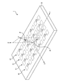
- FIG. 1 is a perspective view of the antenna array 1 of the first embodiment.
- the antenna array 1 is used for transmitting and/or receiving radio waves in the microwave or millimeter wave frequency band.
- this antenna array 1 has a variable directivity in all directions. That is, the antenna array 1 can control the direction with the highest gain (indicated by the arrow A in FIG. 1) in all directions.
- “omnidirectionally” means that when the direction with the highest gain is represented by the vertical angle ⁇ and the horizontal angle ⁇ , not only the vertical angle ⁇ but also the horizontal angle ⁇ is variable.
- the vertical angle ⁇ refers to an inclination angle in the direction with the highest gain with reference to the normal line of the radiation surface of the antenna array 1 (hereinafter referred to as the Z axis).
- the horizontal angle ⁇ refers to a rotation angle around the Z axis in the direction with the highest gain, with reference to an axis orthogonal to the Z axis (hereinafter referred to as the X axis).
- the axis orthogonal to the Z axis and the X axis is called the Y axis.
- the X axis, the Y axis, and the Z axis are orthogonal to each other on the radiation surface.
- the term “horizontal” is used for the horizontal angle ⁇ , but the X axis and the Y axis do not necessarily have to be horizontal. That is, the radiation surface may or may not be horizontal depending on the installation position and orientation of the antenna array 1.
- the antenna array 1 is composed of a sheet-shaped or thin plate-shaped laminated body 2.
- FIG. 2 is a partial cross-sectional view of the laminated body 2.
- the laminated body 2 is arranged in order from the lower layer, that is, in the Z-axis direction in the order of the line pattern layer 20, the first dielectric layer 11, the ground conductor layer 30, the interlayer adhesive layer 12, the second dielectric layer 13, and the antenna pattern layer 40. , An interlayer adhesive layer 14 and a protective dielectric layer 15.
- the first dielectric layer 11 and the second dielectric layer 13 sandwich the conductive ground conductor layer 30 therebetween, and are joined to each other by the interlayer adhesive layer 12.
- the second dielectric layer 13 and the protective dielectric layer 15 sandwich the conductive antenna pattern layer 40 therebetween, and are joined to each other by the interlayer adhesive layer 14.
- the line pattern layer 20 is formed on the surface of the first dielectric layer 11 on the opposite side of the ground conductor layer 30 with respect to the first dielectric layer 11.
- the line pattern layer 20 may be covered with a dielectric protective film.
- the first dielectric layer 11 is made of a dielectric material such as liquid crystal polymer or glass base resin.
- the first dielectric layer 11 may not be a single dielectric layer but may be a laminated body of dielectrics.
- the interlayer adhesive layer 12 is made of a dielectric material.
- the second dielectric layer 13 has a dielectric layer 13a, an interlayer adhesive layer 13b, and a dielectric layer 13c in order from the bottom. The dielectric layer 13a and the dielectric layer 13c are joined to each other by the interlayer adhesive layer 13b sandwiched between them.
- the dielectric layers 13a and 13c are made of a dielectric material such as liquid crystal polymer or glass base resin.
- the interlayer adhesive layer 13b is made of a dielectric material. Note that the second dielectric layer 13 may be a single dielectric layer instead of a dielectric laminate.
- the protective dielectric layer 15 is made of a dielectric material such as liquid crystal polymer or glass base resin.
- FIG. 3 is a plan view of the antenna pattern layer 40.
- the antenna pattern layer 40 is shaped by an additive method or a subtractive method, and the antenna pattern layer 40 has a plurality of antennas 41.
- These antennas 41 are arranged in a two-dimensional array, that is, in a grid or matrix.
- the antennas 41 are arranged in a two-dimensional array with four rows in the X-axis direction and four rows in the Y-axis direction.
- the antennas 41 are arranged along a plane, that is, along the surface of the second dielectric layer 13, and the plane is a radiation surface.
- the X axis, the Y axis, and the Z axis are orthogonal to each other at the center of the region where the antennas 41 are arranged in a two-dimensional array.
- a reference numeral “41” in FIG. 3 is attached with a subscript number, and the subscript number indicates the arrangement order of the antennas 41. That is, when an arbitrary number from 1 to 4 is set as m and n, the antenna 41 (m,n) has the m-th row in the negative X-axis direction and the n-th row in the positive Y-axis direction from the lower left in FIG. It's an eye.
- Each of the antennas 41 (1,1) to 41 (4,4) has patch-type antenna elements 41a and 41b, power feeding branch lines 41c and 41d, and a land portion 41e.
- the antenna element 41a, the land portion 41e, and the antenna element 41b are arranged in this order in a straight line in parallel with the Y-axis at intervals.
- the antenna elements 41a and 41b of these antennas 41 (1,1) to 41 (4,4) are arranged in a two-dimensional array, that is, in a lattice or matrix form (in FIG. 3, four rows in the X-axis direction, 8 rows in the Y-axis direction).
- the feeding branch line 41c is arranged in a region between the antenna element 41a and the land section 41e, the land section 41e is electrically connected to one end of the feeding branch line 41c, and the antenna element 41a is connected to the other end of the feeding branch line 41c. It is electrically connected.
- the power feeding branch line 41d is arranged in a region between the antenna element 41b and the land portion 41e, the land portion 41e is electrically connected to one end of the power feeding branch line 41d, and the antenna element 41b is connected to the other end of the power feeding branch line 41d. It is electrically connected.
- the electrical length of the feeding branch line 41c is shorter than the electrical length of the feeding branch line 41d by one half of the center wavelength.
- the center wavelength is a wavelength corresponding to the center frequency of the band used by the antenna array 1. Note that FIG. 2 shows a portion corresponding to one antenna 41.
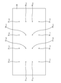
- FIG. 4 is a plan view of the ground conductor layer 30.
- the ground conductor layer 30 is shaped by an additive method, a subtractive method, or the like, so that a plurality of slots 31 are formed in the ground conductor layer 30.
- the slots 31 are arranged in a two-dimensional array, that is, in a grid or matrix so that the slots 31 are individually provided for each antenna 41.
- the slot 31 is arranged in a portion overlapping the land portion 41e in a plan view.
- the plan view means that an object such as the antenna array 1 is viewed in parallel projection in a direction perpendicular to the radiation surface, that is, in the stacking direction of the stacked body 2.
- the reference numeral “31” in FIG. 4 is subscripted. The subscripts indicate the arrangement order of the antennas 41 corresponding to the slots 31.
- FIG. 5 is a plan view of the line pattern layer 20.
- the line pattern layer 20 is shaped by an additive method, a subtractive method, or the like, so that the line pattern layer 20 has a plurality of feed lines 21.
- these power feeding lines 21 are separated from each other and insulated.
- One end 21a of the power supply line 21 is arranged in a two-dimensional array, and in plan view, the one end 21a of the power supply line 21 is arranged at a portion overlapping the slot 31 and the land 41e.
- the reference numeral “21” in FIG. 5 is subscripted.
- the subscript numbers indicate the arrangement order of the antennas 41 corresponding to the power supply lines 21.
- FIG. 6 is a perspective view showing one antenna 41 and the power feeding line 21 corresponding thereto.
- one through-hole conductor 60 is provided for each antenna 41, and a plurality of through-hole conductors 60 are arranged in a two-dimensional array form, that is, a lattice form or a matrix form as a whole.
- One end 21a of the power supply line 21 is individually electrically connected to the land 41e of the antenna 41 by the through-hole conductor 60.
- the through-hole conductor 60 penetrates the first dielectric layer 11, the ground conductor layer 30, the interlayer adhesive layer 12, and the second dielectric layer 13.
- the through-hole conductor 60 is spaced inward from the edge of the slot 31, and the through-hole conductor 60 and the ground conductor layer 30 are electrically insulated from each other. ..
- the through hole conductor 60 may be filled in the through hole or may be plated on the inner wall of the through hole.
- the feed line 21 feeds power individually to each antenna 41 via the through-hole conductors 60.
- the ground conductor layer 30 exists between the antenna 41 and the power feeding line 21 as described above, the electromagnetic waves transmitted and received by the antenna 41 are not affected by the signal wave transmitted by the power feeding line 21. Therefore, it is possible to prevent deterioration of radiation efficiency and disturbance of directivity.
- the antenna 41 and the power supply line 21 are formed on different layers. Therefore, the layout of the antenna 41 and the layout of the feed line 21 can be designed independently of each other. Further, the antennas 41 can be densely arranged and arranged in a two-dimensional array. It is also possible to arrange the same number of power feed lines 21 as the antennas 41 in a state of being insulated from each other. It is also possible to arrange the power supply lines 21 in a state of being separated from each other, and it is possible to prevent interference of signal waves between the power supply lines 21.
- Radio frequency integrated circuit as a transceiver is attached to this antenna array 1.
- the RFIC has at least as many power supply terminals as the power supply lines 21.
- the other end of the power feeding line 21 is individually electrically connected to the power feeding terminal of the RFIC.
- the directivity of the antenna array 1 is controlled by the RFIC individually controlling the phase of the signal wave for each antenna 41 via each feed line 21.
- the mounting location of the RFIC is not particularly limited, but it is surface-mounted on the line pattern layer 20, for example.
- the RFIC supplies signal waves of the same phase to all the antennas 41 (the mutual phase difference between the antennas 41 is at the land portion 41e.
- the vertical angle ⁇ in the direction of highest gain is substantially 0°.
- the RFIC supplies in-phase signal waves to the antennas 41 (1,1) , 41 (1,2) , 41 (1,3) , 41 (1,4) , and the antennas 41 (2,1) , 41 (2,2) , 41 (2,3) , 41 (2,4) are supplied with signal waves of the same phase, and antennas 41 (3,1) , 41 (3,2) , 41 (3,3 ) ) , 41 (3,4) are supplied with in-phase signal waves, and antennas 41 (4,1) , 41 (4,2) , 41 (4,3) and 41 (4,4) are in-phase Supply a signal wave.
- the antennas 41 (1,1) , 41 (1,2) , 41 (1,3) , 41 (1,4) and the antennas 41 (2,1) , 41 (2,2) , 41 (2 ,3) , 41 (2,4) and the phase difference ⁇ x is the antenna 41 (2,1) , 41 (2,2) , 41 (2,3) , 41 (2,4) 41 (3,1) , 41 (3,2) , 41 (3,3) , 41 (3,4) and a phase difference ⁇ x , and antennas 41 (3,1) , 41 ( 3,4) 2) , 41 (3,3) , 41 (3,4) and antenna 41 (4,1) , 41 (4,2) , 41 (4,3) , 41 (4,4)
- the phase difference ⁇ the horizontal angle ⁇ in the direction of the highest gain becomes substantially 0° or 180°, and the vertical angle ⁇ becomes substantially larger than 0°. In the range where the phase difference ⁇ x is ⁇ 180° to 180°, the vertical angle ⁇ increases as the absolute value of the phase difference ⁇ x increases.
- the RFIC supplies the signal waves of the same phase to the antennas 41 (1,1) , 41 (2,1) , 41 (3,1) , 41 (4,1) , and the antennas 41 (1,2) , 41 (2,2) , 41 (3,2) , 41 (4,2) are supplied with signal waves of the same phase, and antennas 41 (1,3) , 41 (2,3) , 41 (3,3 ) ) , 41 (4,3) are supplied with in-phase signal waves, and antennas 41 (1,4) , 41 (2,4) , 41 (3,4) , 41 (4,4) are in-phase Supply a signal wave.
- each antenna 41 has two antenna elements 41a and 41b.
- the number of antenna elements included in each antenna 41 may be one, or may be three or more.
- the number of antenna elements included in the antenna 41 is 2 k (here, k is an integer of 0 or more). In any case, any antenna 41 has the same number of antenna elements.
Landscapes
- Waveguide Aerials (AREA)
- Variable-Direction Aerials And Aerial Arrays (AREA)
Abstract
全方位的に指向性を制御することができるアンテナアレイを提供する。 アンテナアレイ1は、積層順に、複数の給電線路21と、第1の誘電体層11と、地導体層30と、第2の誘電体層13と、複数のアンテナ41と、を備えるとともに、第1の誘電体層11、地導体層30及び第2の誘電体層13を貫通している複数のスルーホール導体60を備える。アンテナ41はアンテナ素子41a,41bを有し、アンテナ素子41a,41bが二次元アレイ状に配列されている。スルーホール導体60が地導体層30から電気的に絶縁した状態で地導体層30を貫通している。複数の給電線路21がそれぞれスルーホール導体60を介してアンテナ41毎に個別に給電する。
Description
本発明は、アンテナアレイに関する。
アンテナアレイ(アレイアンテナともいう)はアンテナ素子を格子状に配列したものである。これらアンテナ素子を励振することによって所望の指向性を得ることができる。アンテナ素子にはマイクロストリップラインが利用されることがある。マイクロストリップライン方式のアンテナ素子は誘電体基板の一方の面にパッチ状に形成されており、誘電体基板の反対側の面には地導体層が形成されている。
一方、特許文献1には、ビームフォーミング技術、つまりアンテナの指向性が可変となる技術が開示されている。
ところで、マイクロストリップラインを利用したアンテナアレイとしては、全方位的に指向性を制御するものはない。
そこで、本発明は、上記事情に鑑みてなされたものであって、全方位的に指向性を制御することができるアンテナアレイを提供することを目的とする。
そこで、本発明は、上記事情に鑑みてなされたものであって、全方位的に指向性を制御することができるアンテナアレイを提供することを目的とする。
上記目的を達成するための主たる発明は、積層順に、複数の給電線路と、第1の誘電体層と、地導体層と、第2の誘電体層と、複数のアンテナと、を備えるとともに、前記第1の誘電体層、前記地導体層及び前記第2の誘電体層を貫通している複数のスルーホール導体を備え、前記各アンテナは少なくとも1つのアンテナ素子を有し、前記アンテナ素子が二次元アレイ状に配列され、前記スルーホール導体が前記地導体層から電気的に絶縁した状態で前記地導体層を貫通し、前記複数の給電線路がそれぞれ前記スルーホール導体を介して前記アンテナ毎に個別に給電するアンテナアレイである。
本発明の他の特徴については、後述する明細書及び図面の記載により明らかにする。
本発明の実施態様によれば、全方位的に指向性を制御可能なアンテナアレイを提供できる。
後述する明細書及び図面の記載から、少なくとも以下の事項が明らかとなる。
積層順に、複数の給電線路と、第1の誘電体層と、地導体層と、第2の誘電体層と、複数のアンテナと、を備えるとともに、前記第1の誘電体層、前記地導体層及び前記第2の誘電体層を貫通している複数のスルーホール導体を備え、前記各アンテナは少なくとも1つのアンテナ素子を有し、前記アンテナ素子が二次元アレイ状に配列され、前記スルーホール導体が前記地導体層から電気的に絶縁した状態で前記地導体層を貫通し、前記複数の給電線路がそれぞれ前記スルーホール導体を介して前記アンテナ毎に個別に給電するアンテナアレイが明らかとなる。
以上によれば、給電線路がそれぞれスルーホール導体を介してアンテナ毎に個別に給電するため、アンテナ毎に個別に位相を制御することができる。そのようなアンテナが二次元アレイ状に配列されているため、アンテナアレイによって送信され又は受信される電磁波の指向性を全方位的に制御することができる。
前記アンテナ毎の前記アンテナ素子の数が同数である。
===実施の形態===
以下、図面を参照して、本発明の実施形態について説明する。但し、以下に述べる実施形態には、本発明を実施するために技術的に好ましい種々の限定が付されているが、本発明の範囲を以下の実施形態及び図示例に限定するものではない。
以下、図面を参照して、本発明の実施形態について説明する。但し、以下に述べる実施形態には、本発明を実施するために技術的に好ましい種々の限定が付されているが、本発明の範囲を以下の実施形態及び図示例に限定するものではない。
図1は、第1実施形態のアンテナアレイ1の斜視図である。
このアンテナアレイ1は、マイクロ波又はミリ波の周波数帯の電波の送信若しくは受信又はこれらの両方に利用される。
また、このアンテナアレイ1は指向性を全方位的に可変なものである。つまり、アンテナアレイ1は、最も利得の高い方向(図1において矢印Aで示す)を全方位的に制御可能なものである。ここで、「全方位的に」とは、最も利得の高い方向を垂直角φ及び水平角θで表した場合、垂直角φのみならず水平角θも可変であることをいう。垂直角φとは、アンテナアレイ1の放射面の法線(以下、Z軸という)を基準として、最も利得の高い方向への傾斜角度をいう。水平角θとは、Z軸に対して直交する軸(以下、X軸という)を基準として、最も利得の高い方向へのZ軸回りの回転角度をいう。Z軸及びX軸に対して直交する軸をY軸という。X軸、Y軸及びZ軸は放射面において互いに直交する。水平角θに「水平」という用語を用いるが、X軸及びY軸は必ずしも水平である必要はない。つまり、アンテナアレイ1の設置位置及び向きに応じて、放射面が水平であったりそうでなかったりする。
アンテナアレイ1はシート状又は薄板状の積層体2からなる。図2は積層体2の部分断面図である。積層体2は下層から順に、つまりZ軸方向の順に線路パターン層20、第1の誘電体層11、地導体層30、層間接着剤層12、第2の誘電体層13、アンテナパターン層40、層間接着剤層14及び保護誘電体層15を有する。
第1の誘電体層11と第2の誘電体層13が、これらの間に導電性の地導体層30を挟み込んで、層間接着剤層12によって互いに接合されている。
第2の誘電体層13と保護誘電体層15が、これらの間に導電性のアンテナパターン層40を挟み込んで、層間接着剤層14によって互いに接合されている。
第1の誘電体層11に関して地導体層30の反対側において、線路パターン層20が第1の誘電体層11の表面に形成されている。この線路パターン層20が誘電体の保護膜によって被覆されてもよい。
第1の誘電体層11は例えば液晶ポリマー又はガラス基材樹脂等の誘電体材料からなる。なお、第1の誘電体層11が誘電体の単層ではなく、誘電体の積層体であってもよい。
層間接着剤層12は誘電体材料からなる。
第2の誘電体層13は下層から順に誘電体層13a、層間接着剤層13b及び誘電体層13cを有する。誘電体層13aと誘電体層13cが、それらの間に挟まれた層間接着剤層13bによって互いに接合されている。誘電体層13a及び誘電体層13cは例えば液晶ポリマー又はガラス基材樹脂等の誘電体材料からなる。層間接着剤層13bは誘電体材料からなる。なお、第2の誘電体層13が誘電体の積層体ではなく、誘電体の単層であってもよい。
保護誘電体層15は例えば液晶ポリマー又はガラス基材樹脂等の誘電体材料からなる。
層間接着剤層12は誘電体材料からなる。
第2の誘電体層13は下層から順に誘電体層13a、層間接着剤層13b及び誘電体層13cを有する。誘電体層13aと誘電体層13cが、それらの間に挟まれた層間接着剤層13bによって互いに接合されている。誘電体層13a及び誘電体層13cは例えば液晶ポリマー又はガラス基材樹脂等の誘電体材料からなる。層間接着剤層13bは誘電体材料からなる。なお、第2の誘電体層13が誘電体の積層体ではなく、誘電体の単層であってもよい。
保護誘電体層15は例えば液晶ポリマー又はガラス基材樹脂等の誘電体材料からなる。
図3はアンテナパターン層40の平面図である。図3に示すように、アンテナパターン層40がアディティブ法又はサブトラクティブ法等によって形状加工されており、これによりアンテナパターン層40は複数のアンテナ41を有する。これらアンテナ41は二次元アレイ状に、つまり格子状又はマトリックス状に配列されている。ここでは、アンテナ41はX軸方向に4列且つY軸方向に4列の二次元アレイ状に配列されている。アンテナ41が平面に沿って、つまり第2の誘電体層13の表面に沿って配列されており、その平面が放射面である。ここで、X軸、Y軸及びZ軸は、アンテナ41が二次元アレイ状に配列された領域の中心において互いに直交する。
図3中の参照符号「41」に下付き数字が付されており、その下付き数字はアンテナ41の配列順を表す。つまり、1から4までの任意の数をm,nとした場合、アンテナ41(m,n)は、図3中の左下からX軸負方向にm列目、且つY軸正方向にn列目である。
各アンテナ41(1,1)~41(4,4)はパッチ型のアンテナ素子41a,41b、給電支線路41c,41d及びランド部41eを有する。
順にアンテナ素子41aとランド部41eとアンテナ素子41bが間隔を置いてY軸と平行に一直線状に配列されている。これらアンテナ41(1,1)~41(4,4)のアンテナ素子41a,41bは二次元アレイ状に、つまり格子状又はマトリックス状に配列されている(図3ではX軸方向に4列、Y軸方向に8列となる)。給電支線路41cがアンテナ素子41aとランド部41eとの間の領域に配置され、ランド部41eが給電支線路41cの一端に電気的に接続され、アンテナ素子41aが給電支線路41cの他端に電気的に接続されている。給電支線路41dがアンテナ素子41bとランド部41eとの間の領域に配置され、ランド部41eが給電支線路41dの一端に電気的に接続され、アンテナ素子41bが給電支線路41dの他端に電気的に接続されている。給電支線路41cの電気長は給電支線路41dの電気長よりも中心波長の2分の1だけ短い。中心波長とは、このアンテナアレイ1の使用帯域の中心周波数に対応する波長である。
なお、図2は、1つのアンテナ41に相当する部分を示す。
順にアンテナ素子41aとランド部41eとアンテナ素子41bが間隔を置いてY軸と平行に一直線状に配列されている。これらアンテナ41(1,1)~41(4,4)のアンテナ素子41a,41bは二次元アレイ状に、つまり格子状又はマトリックス状に配列されている(図3ではX軸方向に4列、Y軸方向に8列となる)。給電支線路41cがアンテナ素子41aとランド部41eとの間の領域に配置され、ランド部41eが給電支線路41cの一端に電気的に接続され、アンテナ素子41aが給電支線路41cの他端に電気的に接続されている。給電支線路41dがアンテナ素子41bとランド部41eとの間の領域に配置され、ランド部41eが給電支線路41dの一端に電気的に接続され、アンテナ素子41bが給電支線路41dの他端に電気的に接続されている。給電支線路41cの電気長は給電支線路41dの電気長よりも中心波長の2分の1だけ短い。中心波長とは、このアンテナアレイ1の使用帯域の中心周波数に対応する波長である。
なお、図2は、1つのアンテナ41に相当する部分を示す。
図4は地導体層30の平面図である。図4に示すように、地導体層30がアディティブ法又はサブトラクティブ法等によって形状加工されており、これにより地導体層30には複数のスロット31が形成されている。スロット31がアンテナ41毎に個別に設けられるべく、スロット31が二次元アレイ状に、つまり格子状又はマトリックス状に配列されている。平面視で、スロット31がランド部41eと重なる部分に配置されている。平面視とは、アンテナアレイ1等の対象物を、放射面に対して垂直な方向、つまり積層体2の積層方向に平行投影的に見ることをいう。
図4中の参照符号「31」に下付き数字が付されている。下付き数字はスロット31にそれぞれ対応するアンテナ41の配列順を表す。
図5は線路パターン層20の平面図である。図5に示すように、線路パターン層20がアディティブ法又はサブトラクティブ法等によって形状加工されており、これにより線路パターン層20が複数の給電線路21を有する。給電線路21がアンテナ41毎に個別に給電すべく、これら給電線路21が互いに離間して絶縁されている。給電線路21の一端部21aが二次元アレイ状に配置され、平面視で、給電線路21の一端部21aがスロット31及びランド部41eと重なる部分に配置されている。
図5中の参照符号「21」に下付き数字が付されている。下付き数字は給電線路21にそれぞれ対応するアンテナ41の配列順を表す。
図6は、1つのアンテナ41とそれに対応する給電線路21を示した斜視図である。図6に示すように1つのアンテナ41につき1つのスルーホール導体60が設けられ、全体として複数のスルーホール導体60が二次元アレイ状、つまり格子状又はマトリックス状に配列されている。給電線路21の一端部21aが個別にスルーホール導体60によってアンテナ41のランド部41eに電気的に接続されている。図2に示すように、スルーホール導体60は第1の誘電体層11、地導体層30、層間接着剤層12及び第2の誘電体層13を貫通している。スルーホール導体60が地導体層30を貫通する箇所では、スルーホール導体60がスロット31の縁から内側に離間しており、スルーホール導体60と地導体層30が互いに電気的に絶縁されている。スルーホール導体60はスルーホール内に充填されていてもよいし、スルーホールの内壁にメッキ等されたものでもよい。給電線路21がそれぞれスルーホール導体60を介してアンテナ41毎に個別に給電する。
以上のようにアンテナ41と給電線路21との間に地導体層30が存在するため、アンテナ41によって送受信される電磁波は給電線路21によって伝送される信号波の影響を受けない。従って、放射効率の低下及び指向性の乱れを防止できる。
アンテナ41と給電線路21が別の層に形成されている。そのため、アンテナ41のレイアウトと給電線路21のレイアウトを相互に独立的に設計することができる。また、アンテナ41を密集させて二次元アレイ状に配列させることもできる。アンテナ41と同数の給電線路21を相互に絶縁させた状態で配置することもできる。給電線路21を相互に離間させた状態で配置することもでき、給電線路21の相互間の信号波の干渉も防止できる。
このアンテナアレイ1には、送受信機としてのRFIC(Radio Frequency Integrated Circuit)が取り付けられている。RFICは、少なくとも、給電線路21と同数の給電端子を有する。給電線路21の他端部が個別にRFICの給電端子に電気的に接続されている。RFICが各給電線路21を介してアンテナ41毎に個別に信号波の位相を制御することによって、アンテナアレイ1の指向性が制御される。RFICの実装場所は特に限定されないが、例えば線路パターン層20に表面実装される。
例えば、RFICが全てのアンテナ41に同位相の信号波(アンテナ41の相互の位相差はランド部41eにおけるもの。以下、同じ。)を供給する。その場合、最も利得の高い方向の垂直角φが実質的に0°になる。
例えば、RFICがアンテナ41(1,1),41(1,2),41(1,3),41(1,4)に同位相の信号波を供給し、アンテナ41(2,1),41(2,2),41(2,3),41(2,4)に同位相の信号波を供給し、アンテナ41(3,1),41(3,2),41(3,3),41(3,4)に同位相の信号波を供給し、アンテナ41(4,1),41(4,2),41(4,3),41(4,4)に同位相の信号波を供給する。この場合、アンテナ41(1,1),41(1,2),41(1,3),41(1,4)とアンテナ41(2,1),41(2,2),41(2,3),41(2,4)との間に位相差Φxが、アンテナ41(2,1),41(2,2),41(2,3),41(2,4)とアンテナ41(3,1),41(3,2),41(3,3),41(3,4)との間に位相差Φxが、更にアンテナ41(3,1),41(3,2),41(3,3),41(3,4)とアンテナ41(4,1),41(4,2),41(4,3),41(4,4)との間に位相差Φがあると、最も利得の高い方向の水平角θが実質的に0°又は180°になり、垂直角φが実質的に0°よりも大きくなる。位相差Φxが-180°~180°の範囲では、位相差Φxの絶対値が大きくなるにつれて、垂直角φが大きくなる。そのことをシミュレーションにより検証した結果を表1に示す。

例えば、RFICがアンテナ41(1,1),41(2,1),41(3,1),41(4,1)に同位相の信号波を供給し、アンテナ41(1,2),41(2,2),41(3,2),41(4,2)に同位相の信号波を供給し、アンテナ41(1,3),41(2,3),41(3,3),41(4,3)に同位相の信号波を供給し、アンテナ41(1,4),41(2,4),41(3,4),41(4,4)に同位相の信号波を供給する。この場合、アンテナ41(1,1),41(2,1),41(3,1),41(4,1)とアンテナ41(1,2),41(2,2),41(3,2),41(4,2)との間に位相差Φyが、アンテナ41(1,2),41(2,2),41(3,2),41(4,2)とアンテナ41(1,3),41(2,3),41(3,3),41(4,3)との間に位相差Φyが、更にアンテナ41(1,3),41(2,3),41(3,3),41(4,3)とアンテナ41(1,4),41(2,4),41(3,4),41(4,4)との間に位相差Φyがあると、最も利得の高い方向の水平角θが90°又は270°になり、垂直角φが0°よりも大きくなる。位相差Φyが-180°~180°の範囲では、位相差Φyの絶対値が大きくなるにつれて、垂直角φが大きくなる。そのことをシミュレーションにより検証した結果を表2に示す。

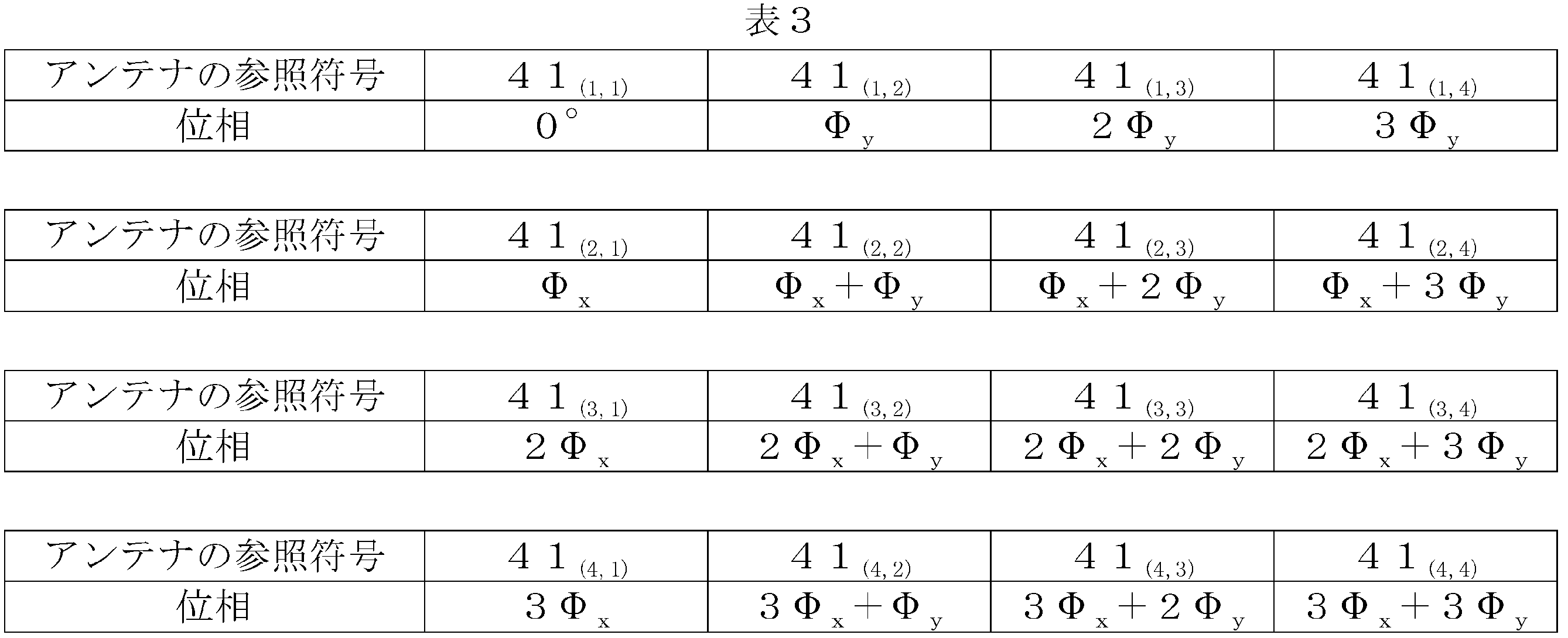
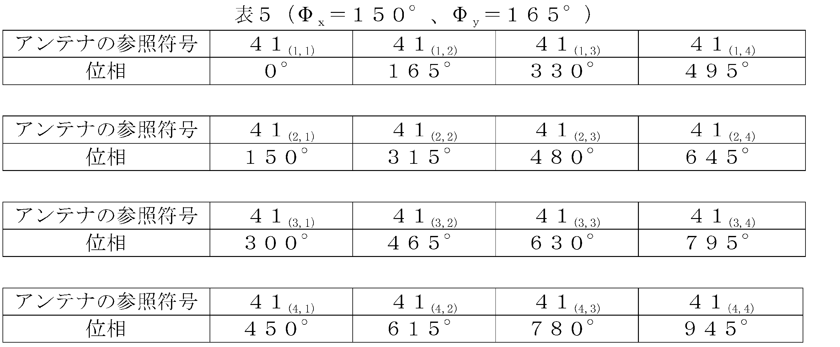
勿論、最も利得の高い方向の水平角θを0°,90°,180°,270°以外にも制御することができる。例えば、アンテナ41(1,1)の位相を基準として、各アンテナ41に表3に示す位相の信号波を供給した場合、具体的には表4及び表5に示す位相の信号波を供給した場合、最も利得の高い方向のベクトルをY軸方向へXZ平面に平行投影したときのZ軸に対するそのベクトルの成す角(以下、XZ平面内の角度という)と、そのベクトルをX軸方向にYZ平面に平行投影したときのZ軸に対するそのベクトルの成す角(以下、YZ平面内の角度という)は表6及び表7のようになる。



上記実施形態では、何れのアンテナ41も2つのアンテナ素子41a,41bを有する。各アンテナ41が有するアンテナ素子の数は1であってもよいし、3以上であってもよい。好ましくは、アンテナ41が有するアンテナ素子の数は2kであることが好ましい(ここで、kは0以上の整数である)。何れにしても、何れのアンテナ41が同数のアンテナ素子を有する。
1…アンテナアレイ
11…第1の誘電体層
13…第2の誘電体層
21…給電線路
30…地導体層
31…スロット
41…アンテナ
41a,41b…アンテナ素子
60…スルーホール導体
11…第1の誘電体層
13…第2の誘電体層
21…給電線路
30…地導体層
31…スロット
41…アンテナ
41a,41b…アンテナ素子
60…スルーホール導体
Claims (2)
- 積層順に、複数の給電線路と、第1の誘電体層と、地導体層と、第2の誘電体層と、複数のアンテナと、を備えるとともに、前記第1の誘電体層、前記地導体層及び前記第2の誘電体層を貫通している複数のスルーホール導体を備え、
前記各アンテナは少なくとも1つのアンテナ素子を有し、前記アンテナ素子が二次元アレイ状に配列され、
前記スルーホール導体が前記地導体層から電気的に絶縁した状態で前記地導体層を貫通し、
前記複数の給電線路がそれぞれ前記スルーホール導体を介して前記アンテナ毎に個別に給電する
アンテナアレイ。 - 前記アンテナ毎の前記アンテナ素子の数が同数である
請求項1に記載のアンテナアレイ。
Applications Claiming Priority (2)
| Application Number | Priority Date | Filing Date | Title |
|---|---|---|---|
| JP2018-227271 | 2018-12-04 | ||
| JP2018227271 | 2018-12-04 |
Publications (1)
| Publication Number | Publication Date |
|---|---|
| WO2020115979A1 true WO2020115979A1 (ja) | 2020-06-11 |
Family
ID=70975028
Family Applications (1)
| Application Number | Title | Priority Date | Filing Date |
|---|---|---|---|
| PCT/JP2019/035131 Ceased WO2020115979A1 (ja) | 2018-12-04 | 2019-09-06 | アンテナアレイ |
Country Status (1)
| Country | Link |
|---|---|
| WO (1) | WO2020115979A1 (ja) |
Citations (3)
| Publication number | Priority date | Publication date | Assignee | Title |
|---|---|---|---|---|
| JPH03125510U (ja) * | 1990-03-30 | 1991-12-18 | ||
| JPH06291544A (ja) * | 1993-04-02 | 1994-10-18 | Tech Res & Dev Inst Of Japan Def Agency | アレイアンテナ装置 |
| JP2018186337A (ja) * | 2017-04-24 | 2018-11-22 | 株式会社村田製作所 | アレーアンテナ |
-
2019
- 2019-09-06 WO PCT/JP2019/035131 patent/WO2020115979A1/ja not_active Ceased
Patent Citations (3)
| Publication number | Priority date | Publication date | Assignee | Title |
|---|---|---|---|---|
| JPH03125510U (ja) * | 1990-03-30 | 1991-12-18 | ||
| JPH06291544A (ja) * | 1993-04-02 | 1994-10-18 | Tech Res & Dev Inst Of Japan Def Agency | アレイアンテナ装置 |
| JP2018186337A (ja) * | 2017-04-24 | 2018-11-22 | 株式会社村田製作所 | アレーアンテナ |
Similar Documents
| Publication | Publication Date | Title |
|---|---|---|
| US11177582B2 (en) | Dual polarized antenna and dual polarized antenna assembly comprising same | |
| CN110574236B (zh) | 一种液晶可重构多波束相控阵列 | |
| EP3401999B1 (en) | Luneberg lens antenna device | |
| US10749267B2 (en) | Antenna device for vehicle | |
| US10230174B2 (en) | Frequency diverse phased-array antenna | |
| US20190356058A1 (en) | Antenna element having a segmentation cut plane | |
| US11233310B2 (en) | Low-profile conformal antenna | |
| JP2016127474A (ja) | 偏波共用アンテナ | |
| US12272878B2 (en) | Composite antenna element design and method for beamwidth control | |
| CN112703638B (zh) | 具有独立旋转的辐射元件的天线阵列 | |
| US20190334255A1 (en) | Modular/scalable antenna array design | |
| US10886604B2 (en) | Interleaved array of antennas operable at multiple frequencies | |
| JP7009031B2 (ja) | 円偏波共用平面アンテナ | |
| US10461417B2 (en) | Power feed circuit and antenna device | |
| CN115939741A (zh) | 超低成本一维扫描天线阵列 | |
| JP6630773B2 (ja) | アンテナ | |
| JP2019220886A (ja) | パッチアンテナ及びこれを備えるアンテナモジュール | |
| JP2023166326A (ja) | アンテナ装置及び無線通信装置 | |
| US20240128658A1 (en) | Dual polarization antenna and dual polarization antenna assembly comprising same | |
| WO2005083840A1 (ja) | トリプレート型平面アレーアンテナ | |
| KR102638563B1 (ko) | 반사판을 갖는 패치 안테나 | |
| JP7591401B2 (ja) | アレイアンテナ | |
| JP6890155B2 (ja) | アレイアンテナ | |
| JP5918874B1 (ja) | アレイアンテナ | |
| US9356360B1 (en) | Dual polarized probe coupled radiating element |
Legal Events
| Date | Code | Title | Description |
|---|---|---|---|
| 121 | Ep: the epo has been informed by wipo that ep was designated in this application |
Ref document number: 19893976 Country of ref document: EP Kind code of ref document: A1 |
|
| NENP | Non-entry into the national phase |
Ref country code: DE |
|
| 122 | Ep: pct application non-entry in european phase |
Ref document number: 19893976 Country of ref document: EP Kind code of ref document: A1 |
|
| NENP | Non-entry into the national phase |
Ref country code: JP |