WO2020111690A1 - 멀티 프로버용 척 조립체 및 채널 - Google Patents
멀티 프로버용 척 조립체 및 채널 Download PDFInfo
- Publication number
- WO2020111690A1 WO2020111690A1 PCT/KR2019/016249 KR2019016249W WO2020111690A1 WO 2020111690 A1 WO2020111690 A1 WO 2020111690A1 KR 2019016249 W KR2019016249 W KR 2019016249W WO 2020111690 A1 WO2020111690 A1 WO 2020111690A1
- Authority
- WO
- WIPO (PCT)
- Prior art keywords
- chuck assembly
- chuck
- channel
- heater
- substrate
- Prior art date
- Legal status (The legal status is an assumption and is not a legal conclusion. Google has not performed a legal analysis and makes no representation as to the accuracy of the status listed.)
- Ceased
Links
Images


Classifications
-
- G—PHYSICS
- G01—MEASURING; TESTING
- G01R—MEASURING ELECTRIC VARIABLES; MEASURING MAGNETIC VARIABLES
- G01R31/00—Arrangements for testing electric properties; Arrangements for locating electric faults; Arrangements for electrical testing characterised by what is being tested not provided for elsewhere
- G01R31/28—Testing of electronic circuits, e.g. by signal tracer
- G01R31/2851—Testing of integrated circuits [IC]
- G01R31/2855—Environmental, reliability or burn-in testing
- G01R31/286—External aspects, e.g. related to chambers, contacting devices or handlers
- G01R31/2863—Contacting devices, e.g. sockets, burn-in boards or mounting fixtures
-
- G—PHYSICS
- G01—MEASURING; TESTING
- G01R—MEASURING ELECTRIC VARIABLES; MEASURING MAGNETIC VARIABLES
- G01R1/00—Details of instruments or arrangements of the types included in groups G01R5/00 - G01R13/00 and G01R31/00
- G01R1/02—General constructional details
- G01R1/06—Measuring leads; Measuring probes
- G01R1/067—Measuring probes
- G01R1/073—Multiple probes
- G01R1/07307—Multiple probes with individual probe elements, e.g. needles, cantilever beams or bump contacts, fixed in relation to each other, e.g. bed of nails fixture or probe card
-
- G—PHYSICS
- G01—MEASURING; TESTING
- G01R—MEASURING ELECTRIC VARIABLES; MEASURING MAGNETIC VARIABLES
- G01R31/00—Arrangements for testing electric properties; Arrangements for locating electric faults; Arrangements for electrical testing characterised by what is being tested not provided for elsewhere
- G01R31/28—Testing of electronic circuits, e.g. by signal tracer
- G01R31/2851—Testing of integrated circuits [IC]
- G01R31/2855—Environmental, reliability or burn-in testing
- G01R31/286—External aspects, e.g. related to chambers, contacting devices or handlers
- G01R31/2865—Holding devices, e.g. chucks; Handlers or transport devices
-
- G—PHYSICS
- G01—MEASURING; TESTING
- G01R—MEASURING ELECTRIC VARIABLES; MEASURING MAGNETIC VARIABLES
- G01R31/00—Arrangements for testing electric properties; Arrangements for locating electric faults; Arrangements for electrical testing characterised by what is being tested not provided for elsewhere
- G01R31/28—Testing of electronic circuits, e.g. by signal tracer
- G01R31/2851—Testing of integrated circuits [IC]
- G01R31/2855—Environmental, reliability or burn-in testing
- G01R31/2872—Environmental, reliability or burn-in testing related to electrical or environmental aspects, e.g. temperature, humidity, vibration, nuclear radiation
- G01R31/2879—Environmental, reliability or burn-in testing related to electrical or environmental aspects, e.g. temperature, humidity, vibration, nuclear radiation related to electrical aspects, e.g. to voltage or current supply or stimuli or to electrical loads
-
- G—PHYSICS
- G01—MEASURING; TESTING
- G01R—MEASURING ELECTRIC VARIABLES; MEASURING MAGNETIC VARIABLES
- G01R31/00—Arrangements for testing electric properties; Arrangements for locating electric faults; Arrangements for electrical testing characterised by what is being tested not provided for elsewhere
- G01R31/28—Testing of electronic circuits, e.g. by signal tracer
- G01R31/2851—Testing of integrated circuits [IC]
- G01R31/2886—Features relating to contacting the IC under test, e.g. probe heads; chucks
-
- H—ELECTRICITY
- H10—SEMICONDUCTOR DEVICES; ELECTRIC SOLID-STATE DEVICES NOT OTHERWISE PROVIDED FOR
- H10P—GENERIC PROCESSES OR APPARATUS FOR THE MANUFACTURE OR TREATMENT OF DEVICES COVERED BY CLASS H10
- H10P72/00—Handling or holding of wafers, substrates or devices during manufacture or treatment thereof
- H10P72/70—Handling or holding of wafers, substrates or devices during manufacture or treatment thereof for supporting or gripping
-
- G—PHYSICS
- G01—MEASURING; TESTING
- G01R—MEASURING ELECTRIC VARIABLES; MEASURING MAGNETIC VARIABLES
- G01R31/00—Arrangements for testing electric properties; Arrangements for locating electric faults; Arrangements for electrical testing characterised by what is being tested not provided for elsewhere
- G01R31/28—Testing of electronic circuits, e.g. by signal tracer
- G01R31/2851—Testing of integrated circuits [IC]
- G01R31/2855—Environmental, reliability or burn-in testing
- G01R31/2872—Environmental, reliability or burn-in testing related to electrical or environmental aspects, e.g. temperature, humidity, vibration, nuclear radiation
- G01R31/2874—Environmental, reliability or burn-in testing related to electrical or environmental aspects, e.g. temperature, humidity, vibration, nuclear radiation related to temperature
-
- G—PHYSICS
- G01—MEASURING; TESTING
- G01R—MEASURING ELECTRIC VARIABLES; MEASURING MAGNETIC VARIABLES
- G01R31/00—Arrangements for testing electric properties; Arrangements for locating electric faults; Arrangements for electrical testing characterised by what is being tested not provided for elsewhere
- G01R31/28—Testing of electronic circuits, e.g. by signal tracer
- G01R31/2851—Testing of integrated circuits [IC]
- G01R31/2886—Features relating to contacting the IC under test, e.g. probe heads; chucks
- G01R31/2891—Features relating to contacting the IC under test, e.g. probe heads; chucks related to sensing or controlling of force, position, temperature
Definitions
- the present invention relates to a chuck assembly and channel for a multi-prover.
- semiconductor devices such as integrated circuit devices can be formed by repeatedly performing a series of semiconductor processes on a semiconductor wafer. For example, a deposition process for forming a thin film on a wafer, an etching process for forming a thin film into patterns having electrical characteristics, an ion implantation process or diffusion process for implanting or diffusing impurities into the patterns, a wafer on which patterns are formed Semiconductor circuit elements may be formed on the wafer by repeatedly performing a cleaning and rinsing process to remove impurities from the wafer.
- an inspection process for inspecting the electrical characteristics of the semiconductor devices may be performed.
- the inspection process may be performed by a probe station comprising a probe card with a plurality of probes and a tester connected to the probe card to provide electrical signals.
- Conventional general substrate inspection apparatus can inspect one substrate at one time. This is called a single probe device.
- a substrate is first placed on a substrate chuck when inspecting the substrate.
- the substrate is transferred from the cassette to the stage. After this, the substrate is aligned by moving the stage to make the substrate contact the probe card.
- the probe card is contacted with the substrate placed on the substrate chuck to inspect the substrate using a tester.
- the single probe device described above can inspect only one substrate at a time, the inspection time is long.
- the inspection time has a disadvantage in that it takes longer than the substrate production amount and has a limitation in the total production time of the throughput.
- One embodiment of the present invention is to provide a chuck assembly for a multi-prover that can electrically test multiple wafers at the same time.
- One embodiment of the present invention is to provide a chuck assembly and channel for a multi-prover that can reduce electromagnetic noise and leakage current that may be generated as the test throughput of the multi-prover increases.
- a multi-prover chuck assembly comprising: a chuck supporting a wafer; A prop card structure coupled to the upper part of the chuck; A heater that heats the chuck under the chuck; It includes a conductive guard plate that is spaced apart from the heater under the heater, and a body portion located under the chuck so that the heater and the guard plate are located inside, and the prop card structure and the body portion are mechanically coupled.
- a chuck assembly formed to have a cartridge-like structure is provided.
- it may further include an insulating member disposed between the heater and the chuck.
- a heat insulating member disposed between the lower portion of the heater and the conductive guard plate may be further included.
- the heater may be shielded by a conductive metal plate and connected to an AC power source.
- two or more conductive guard plates may be formed, and the two or more conductive guard plates may be spaced apart from each other.
- the chuck and the conductive guard plate may be electrically separated and separated by an insulating non-conductor.
- it may further include a grounding member disposed under the guard plate.
- the probe card structure the substrate; It may include a probe formed on the substrate and disposed to face the wafer on the chuck, and a reinforcement portion having a larger area than the substrate and supporting the substrate.
- the reinforcing portion may include an upper reinforcing member positioned on the upper surface of the substrate and a lower reinforcing member positioned under the lower surface of the substrate.
- the locking portion is an upper locker formed below the reinforcing portion; It includes a lower locker formed on the upper portion of the body portion, the upper locker and the lower locker may be formed with a fastening portion that can be mutually fastened by relative rotation between the probe card structure and the body portion.
- a plurality of locking parts may be formed along the outer circumference of the substrate.
- it may further include a chuck assembly locker formed on the reinforcement portion to move the chuck assembly.
- the body portion of the plate-shaped first body A second body spaced downward from the first body; An inner body coupled between the first body and the second body, and a rotating body coupled between the first body and the second body so as to be rotatable about the inner body, wherein the lower locker rotates It can be arranged on the upper surface of the body.
- the first body may further include a body support for spaced apart from the heater.
- the first body, the second body, the inner body and the rotating body may be formed in a ring shape.
- the channel housing having an inner space in which the above-described chuck assembly can be seated;
- a pair of guides formed on both sidewalls inside the channel housing so that the chuck assembly can be guided into the space inside the channel housing;
- a channel is provided on the bottom surface of the channel housing and includes a chuck assembly adjustment portion for adjusting the position of the chuck assembly so that the chuck assembly is seated.
- the channel may further include a guide moving portion for moving the height of the guide in the vertical direction.
- the channel housing may be electrically connected to the AC power neutral line (AC Neutral) and one-point (One-point grounding) to externally shield the chuck assembly from the outside.
- AC Neutral AC power neutral line
- one-point One-point grounding
- the chuck assembly adjusting unit may include a driving unit capable of moving the chuck assembly in the x-axis, y-axis, and z-axis directions.
- the channel housing may be provided with a door through which the chuck assembly can enter and exit on one side.
- the channel housing may be formed with an opening through which a signal line connected to the chuck assembly or a cable connected to the chuck assembly adjusting part penetrates the other side.
- the channel housing may be provided as a hexahedral metallic case.
- a chuck assembly for a multi-prover and a channel for a multi-prover are provided.
- the chuck assembly according to an embodiment of the present invention may be suitable for a multi-prover by mechanically coupling a probe card structure, a chuck, and a body portion to a cartridge shape.
- chuck assembly is mechanically coupled by the locking portion to the probe card structure and the body portion with the chuck on which the wafer is placed, a simple locking structure is provided to facilitate coupling and separation.
- the channel for a multi-prover has a chuck assembly built-in and can be fixed inside the channel, so it can be safely moved even when moving, and the channel is AC shielded to achieve electrical shielding from the outside.
- the chuck assembly may form a guard plate and a grounding member under the heater to suppress noise and leakage current generated by the heater coupled to the wafer chuck.
- the chuck assembly according to an embodiment of the present invention has an effect of suppressing leakage current by introducing a guard plate using air as a dielectric constant value.
- the chuck assembly according to an embodiment of the present invention can minimize EMI/EMS noise such as inductive noise and conductive noise by shielding the heater with a metallic conductor and being connected to an AC power source.
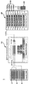
- FIG. 1 is a conceptual diagram of a multi-prover to which a channel and chuck assembly for a multi-prover according to an embodiment of the present invention is applied.
- FIG. 2 is a view showing a form in which a multi-prover channel is stacked according to an embodiment of the present invention.
- FIG. 3 is a block diagram of a multi-prover channel and chuck assembly according to an embodiment of the present invention.
- FIG. 4 is a perspective view showing a state in which a chuck assembly is inserted into a channel for a multi-prover according to an embodiment of the present invention.
- FIG. 5 is a front view of the channel for a multi-prover according to an embodiment of the present invention, in which a chuck assembly is inserted, and partially cut one side of the channel.
- FIG. 6 is an enlarged view of part A in FIG. 5.
- FIG. 7 is a cross-sectional view of a portion of a multi-prover chuck assembly according to an embodiment of the present invention.
- FIG. 8 is a cross-sectional view of another part of a chuck assembly for a multi-prover according to an embodiment of the present invention.
- 1 is a conceptual diagram of a multi-prover to which a channel and chuck assembly for a multi-prover according to an embodiment of the present invention is applied.
- 2 is a view showing a form in which a multi-prover channel is stacked according to an embodiment of the present invention.
- a multi-prover (1) to which a channel and chuck assembly for a multi-prover according to an embodiment of the present invention is applied is for electric testing of multiple wafers 4 at the same time.
- the multi-prover (1) probe probe card (Probe-card) (2), a wafer (4) and a chuck (Chuck) (6) in advance a plurality of After preparation, one cartridge is manufactured by combining one probe card (2), one wafer (4), and one chuck (6), which is the basic unit of the electrical test, in the form of a cartridge.
- the aligner 10 is provided to couple one probe card 2, one wafer 4 and one chuck 6 into a cartridge-type chuck assembly.
- Each of the plurality of chuck assemblies coupled by the aligner 10 may be sequentially put into the chamber 20 composed of a plurality of channels 100a, 100b, 100c, and 100d, and multi-tests may be simultaneously performed. At this time, one cartridge type chuck assembly may be loaded in one channel. At this time, a plurality of channels (100a, 100b, 100c, 100d) in the chamber can be connected to the external connector is connected to the signal connector (24).
- the multi-prover chamber 20 may be made of a plurality of channels (100a, 100b, 100c, 100d) in a stacked form, when loading the chuck assembly to the channel 100, the channel 100
- the test can be performed by loading the chuck assembly that has been assembled in the order of empty channels.
- the multi-prover 1 since a plurality of chuck assemblies can be loaded into a plurality of channels 100a, 100b, 100c, and 100d for testing, the multi-prover 1 has an advantage in that test throughput is significantly increased. On the other hand, as the number of channels increases, so does the number of test ports. At this time, the electromagnetic wave (EMI/EMS) noise and leakage current increased in proportion to the increased number of channels should be reduced.
- EMI/EMS electromagnetic wave
- Chuck assembly and channel according to an embodiment of the present invention provides a structure that can suppress the noise and leakage current in such a multi-prover (1).
- a chuck assembly and a channel according to an embodiment of the present invention will be described in more detail by changing the drawings.
- FIG. 3 is a schematic configuration diagram of a channel 100 and a chuck assembly 200 for a multi-prover according to an embodiment of the present invention.
- 4 is a perspective view showing a state in which the chuck assembly 200 is inserted into the multi-prover channel 100 according to an embodiment of the present invention.
- FIG. 5 is a front view of a channel in which the chuck assembly 200 is inserted in the channel 100 for a multi-prover according to an embodiment of the present invention.
- 6 is an enlarged view of part A in FIG. 5.
- 7 is a cross-sectional view of a portion of a multi-prover chuck assembly 200 according to an embodiment of the present invention.
- FIG. 8 is a cross-sectional view of another part of the chuck assembly 200 for a multi-prover according to an embodiment of the present invention.
- 9 is a comparison graph of noise before and after the leakage current is blocked by the multi-prover chuck assembly 200 and the channel 100 according to an embodiment of the present invention.
- the chuck assembly 200 for a multi-prover may be loaded inside the multi-prover channel 100 after assembly.
- the structure of the chuck assembly 200 will be described after the channel 100 is first described.
- the channel 100 into which the chuck assembly 200 can be loaded includes a channel housing having an inner space in which the chuck assembly 200 can be seated ( 110).
- the channel housing 110 may be provided as a hexahedral metallic case.
- the channel housing 110 may be made lighter using electroless nickel plated aluminum and may be surface treated to have electrical conductivity.
- the channel housing 110 provided as a metallic case may be one-point grounded with an AC neutral filtered by a filter having an inductance of AC power. Accordingly, when the chuck assembly 200 is loaded inside the channel housing 110, the chuck assembly 200 may be electrically shielded from the outside of the channel housing 110.
- the front side of the channel housing 110 is provided with a door 111 through which the chuck assembly 200 can enter and exit, and a signal line connected to the chuck assembly 200 inserted therein at one side surface or a driving part inside the channel housing An opening 112 through which a power cable or a signal cable is penetrated may be formed.
- a pair of guides 120 for guiding the chuck assembly 200 on both sides of the channel housing 110 in the direction in which the chuck assembly 200 is inserted may be installed. Accordingly, both ends of the chuck assembly 200 are guided by a pair of guides 120 so that the chuck assembly 200 can be inserted into the channel housing 110.
- the pair of guides 120 may be supported by the guide moving part 122 so that the height can be moved in the vertical direction from the inside of the channel housing 110.
- the guide moving unit 122 for moving the guide 120 may be implemented by a linear motor or the like, but is not limited thereto.
- a chuck assembly adjustment unit 130 on which the chuck assembly 200 is mounted is provided on the bottom surface of the channel housing 110.
- the chuck assembly adjusting unit 130 may be implemented as a driving unit capable of moving the position of the chuck assembly 200 in the x-axis, y-axis, and z-axis directions, that is, a moving stage.
- a moving stage may be made of a moving stage having various known structures, and detailed description thereof will be omitted herein.
- the chuck assembly 200 inserted into the channel housing 110 along the pair of guides 120 is seated on the chuck assembly adjustment unit 130 and then inside the channel housing 110 In the position can be fixed.
- the chuck assembly 200 fixed to the position inside the channel housing 110 may be stably moved together with the channel housing 110 even if it is moved together with the channel housing 110.
- Chuck assembly 200 according to an embodiment of the present invention that can be loaded into the channel having the above structure, as can be seen from FIGS. 3 to 5, chuck 206, probe card structure 202 ), a heater 230, a conductive guard plate 250, and a body portion 270.
- the probe card structure 202 and the body portion 270 may be formed to have a cartridge type structure by being mechanically coupled.
- the probe card structure 202 may include a substrate 210, a probe 212, and a substrate reinforcement 214.
- the substrate 210 is formed of a PCB substrate, and may be formed in a circular plate shape.
- a plurality of probes 212 may be formed to protrude in the direction toward the wafer 204 on the lower surface of the substrate 210. At this time, various elements inside the wafer 204 may be tested using a plurality of probes 212.
- the substrate reinforcement 214 includes an upper reinforcement member 214a coupled on the upper surface of the substrate 210 and a lower reinforcement member 214b coupled on the lower surface of the substrate 210, and the substrate 210 It is possible to prevent bending due to an external force during the movement or in the stopped state.
- the upper reinforcing member 214a of the substrate reinforcing member 214 may be formed of a plate-like member having a square plane, and both corner portions of the upper reinforcing member 214a are guides in the channel housing 110. It is inserted into the 120 so that the chuck assembly 200 can move along the guide 120 when the chuck assembly 200 moves within the channel housing 110.
- a chuck assembly locker 216 is formed on an upper portion of the upper reinforcement member 214a so that the chuck assembly 200 can be moved in a cartridge state to be coupled to a transport robot (not shown).
- the lower reinforcement member 214b is coupled to the lower surface of the substrate 210 and may be formed in a ring shape.
- the upper locker 282 of the locking portion 280 which will be described later, is positioned below the lower reinforcing member 214b.
- the chuck 206 is formed in a cylindrical shape and may have a seating surface on which the wafer 4 is located.
- the chuck 206 may be made lighter using, for example, electroless nickel plated aluminum, and surface treated to have electrical conductivity. At this time, the chuck 206 may operate as a signal line (+ pole, Signal-line).
- An insulating member 220 may be provided under the chuck 206 to insulate the chuck 206 from the outside.
- a heater 230 may be disposed under the insulating member 220. At this time, the heater 230 is provided to heat the chuck 206, and a heat insulating member 240 is provided below the heater 230 so that heat of the heater 230 can be transmitted only in the chuck direction. Can be.
- the heater 230 has a conductive metal plate on both sides of the upper and lower surfaces to AC-shield electromagnetic noise (EMI/EMS) generated in the heater 230, and the heater shield plate (232 of FIG. 8) ).
- EMI/EMS AC-shield electromagnetic noise
- the heater shielding plate 232 may be connected to a filtered neutral wire of AC power and zero-crossing power conversion power may be used so that there is no switching noise to the power of the heater 230.
- One or more conductive guard plates 250 may be installed under the heater 230.
- the chuck assembly 200 discloses a structure in which two conductive guard plates 252 and 254 are provided.
- the first guard plate 252 and the second guard plate 254 are spatially spaced apart from the heater 230. At this time, the distance between the two guard plates 252. 254 may be 2 to 5 mm, but is not limited thereto.
- the plurality of guard plates 252 and 254 are spaced apart in the air under the heater 230 to form the air as a medium.
- the number of guard plates 250 to be stacked and the separation distance may of course be selected experimentally.
- the guard support 256 may be disposed between the heater 230 and the guard plate 250 and neighboring guard plates to space the plurality of guard plates 250 apart.
- the guard support 256 is preferably formed of a heat insulating material having no electrical conductivity and thermal conductivity.
- a conductive metal grounding member 260 may be provided below the plurality of guard plates 250 for signal grounding.
- the grounding member 260 may act as a (-) pole.
- the ground member 260 may be used, such as a copper plate having low electrical resistance and excellent conductivity, but is not limited thereto.
- the position, quantity, and shape of the plurality of guard plates 250 and the grounding member 260 may be variously changed according to the type of noise.
- the body portion 270 is provided under the chuck 206 to position the heater 230, the plurality of guard plates 250, and the grounding member 260 under the chuck 206. do.
- the probe card structure 202 and the body portion 270 are mechanically coupled to form the chuck assembly 200 to have a cartridge-like structure.
- the body portion 270 may include a first body 272, a second body 274, an inner body 276 and a rotating body 278. .
- the first body 272 may be formed in a circular or ring-shaped plate shape.
- the first body 272 is made of a metal material having a predetermined thickness, so that the inside of the body portion 270 equipped with a heater 230, a guard plate 250, etc. of the cartridge type chuck assembly 200 is protected. Make it possible.
- One or more body portion supports 290 may be disposed between the first body 272 and the heater 230 to maintain a gap between the first body 272 and the heater 230. This is to maintain a space for the guard plate 250 and the ground member 260 between the heater 230 and the first body 272.
- the second body 274 is spaced apart from the first body 272 in a downward direction.
- the second body 274 is formed in a circular or ring shape and may be formed in a plate shape having a predetermined thickness.
- An inner body 276 made of a circular or ring-shaped plate may be fixed between the first body 272 and the second body 274.
- a rotating body 278 may be rotatably coupled to the outer circumference of the inner body 276.
- the rotating body 278 may be formed of a ring-shaped plate member.
- the thickness of the rotating body 278 may correspond to the thickness of the inner body 276.
- a rotating bearing 277 is positioned between the rotating body 278 and the inner body 276 so that the rotating body 278 can rotate around the inner body 276.
- the rotating body 278 is formed to rotate relative to the inner body 276 so that the upper locker 282 and the lower locker 284 of the locking portion 280, which will be described later, can be mutually fastened or released. .
- the outer circumferential portion of the rotating body 278 is formed to have a larger diameter than the first body 272 and the second body 274, the outer circumference of the outer portion than the first body 272 and the second body 274 It is formed to protrude in the direction.
- a ring-shaped partition 279 protruding in the chuck direction may be coupled to the upper surface of the outer circumference of the rotating body 278.
- the guard plate 250 and the grounding member 260 may be protected from the outside under the chuck 206 by the ring-shaped partition 279.
- a locking portion 280 is formed between the substrate reinforcement portion 214 and the body portion 270 of the probe card structure 202.
- the locking portion 280 includes an upper locker 282 formed under the lower reinforcement member 214b of the probe card structure 202 and a lower locker 284 formed over the ring-shaped partition 279 of the body portion 270. ).
- the upper locker 282 and the lower locker 284 are formed with fastening parts that can be fastened to each other by relative rotation between the probe card structure 202 and the body part 270.
- the fastening portion may include a first protrusion 282a protruding in the transverse direction from the upper locker 282 and a second protrusion 284a protruding in the opposite direction from the first protrusion 282a in the lower locker 284. .
- the probe card structure 202 is disposed. Rotating the body portion 270 with a predetermined angle in the left direction when viewed in FIG. 6, the probe card structure 202 and the body are in contact with the top surface of the first protrusion 282a and the bottom surface of the second protrusion 284a. The fastening between the parts 270 is made.
- the body portion 270 is formed of a metal material to have a predetermined weight, and the upper locker 282 and the lower locker 284 are fastened by the weight of the body portion 270. It is formed to be locked by gravity.
- the first protrusion ((282a) and the second protrusion (284a) are not in contact with each other, and the first protrusion (282a) and the second protrusion (284a) are not in contact with the probe card structure 202 and the body part ( 270) can be separated from each other.
- a plurality of locking portions 280 are spaced apart along the outer circumferential portion of the substrate 210 in the circumferential direction on the lower reinforcement member 214b and the ring-shaped partition 279 of the probe card structure 202. Can be.
- the chuck assembly 200 When the probe card structure 202 is coupled to the body portion 270 by the locking structure of the locking portion 280, the chuck assembly 200 may be assembled in the form of a cartridge. Assembly of the probe card structure 202 and the body portion 270 may be made in the aligner 10 as described above, and the cartridge-type chuck assembly assembled in the aligner 10 is moved into the channel by a transfer robot. After being moved, a subsequent process can be performed.
- one or two or more guard plates are installed between the chuck and the grounding member of the chuck assembly, so that the wafer is not only electrically protected from disturbance, but also between the chuck (+ pole) and the grounding member (- pole).
- the noise current of the leakage current was generated from -1.5 pA to 2 pA before the leakage current was shielded in the chuck assembly and channel for a multi-prover according to an embodiment of the present invention.
- the noise current of the leakage current is generated within 0.5 pA until the initial stabilization time (within 5 minutes) after shielding the leakage current, and hardly occurs within 0.3 pA after the stabilization time.
Landscapes
- Engineering & Computer Science (AREA)
- Physics & Mathematics (AREA)
- General Physics & Mathematics (AREA)
- Computer Hardware Design (AREA)
- Microelectronics & Electronic Packaging (AREA)
- General Engineering & Computer Science (AREA)
- Environmental & Geological Engineering (AREA)
- Health & Medical Sciences (AREA)
- Toxicology (AREA)
- Testing Or Measuring Of Semiconductors Or The Like (AREA)
Abstract
멀티 프로버용 척 조립체 및 채널이 제공된다. 본 발명의 일 실시예에 따른 멀티 프로버용 척 조립체는 웨이퍼를 지지하는 척; 척 상부에 결합되는 프로프 카드 구조체; 척 하부에서 척을 히팅하는 히터; 히터의 하부에 히터로부터 이격 배치되는 도전성 가드판 및, 히터 및 가드판이 내부에 위치되도록 척 하부에 위치되는 몸체부를 포함하며, 프로프 카드 구조체 및 몸체부가 기계적으로 결합되어 카트리지형 구조를 갖도록 형성된다.
Description
본 발명은 멀티 프로버용 척 조립체 및 채널에 대한 것이다.
일반적으로 집적 회로 소자들과 같은 반도체 소자들은 반도체 웨이퍼 상에 일련의 반도체 공정들을 반복적으로 수행함으로써 형성될 수 있다. 예를 들면, 웨이퍼 상에 박막을 형성하는 증착 공정, 박막을 전기적 특성들을 갖는 패턴들로 형성하기 위한 식각 공정, 패턴들에 불순물들을 주입 또는 확산시키기 위한 이온 주입 공정 또는 확산 공정, 패턴들이 형성된 웨이퍼로부터 불순물들을 제거하기 위한 세정 및 린스 공정 등을 반복적으로 수행함으로써 반도체 회로 소자들이 웨이퍼 상에 형성될 수 있다.
이러한 일련의 공정들을 통해 반도체 소자들을 형성한 후 반도체 소자들의 전기적인 특성을 검사하기 위한 검사 공정이 수행될 수 있다. 검사 공정은 복수의 탐침들을 갖는 프로브 카드를 포함하는 프로브 스테이션과 전기적인 신호를 제공하기 위하여 프로브 카드와 연결된 테스터에 의해 수행될 수 있다.
종래의 일반적인 기판 검사 장치는 1회 검사 시 하나의 기판을 검사 할 수 있다. 이를 싱글 프로브 장치라 하는데, 싱글 프로브 장치는 기판 검사 시 먼저 기판을 기판 척에 올려놓는다. 기판은 카세트에서 스테이지로 이송된다. 이 후, 기판을 프로브 카드와 접촉 시키기 위해 스테이지를 이동시켜 기판을 정렬시킨다. 기판 척 상에 놓인 기판에 프로브 카드를 접촉시켜 테스터기를 이용해 기판을 검사한다.
상술한 싱글 프로브 장치는 한번에 하나의 기판만을 검사할 수 있어 그 검사 시간이 오래 걸린다. 또한, 상기 검사 시간은 기판 생산량에 비해서 오래 걸려 처리량의 총 생산 시간에 한계가 있는 단점이 있다.
이와 같은 문제를 해결하기 위하여 한번에 동시에 여러 장의 웨이퍼를 전기시험하기 위하여 멀티프로버의 개발이 필요한 실정이다.
본 발명의 일 실시예는 동시에 여러장의 웨이퍼를 전기 시험할 수 있는 멀티 프로버용 척 조립체를 제공하고자 한다.
또한, 멀티 프로버용 척 조립체를 수용할 수 있는 멀티 프로버용 채널을 제공하고자 한다.
본 발명의 일 실시예는 멀티 프로버의 테스트 처리량이 증가됨에 따라 발생될 수 있는 전자파 노이즈 및 누설 전류를 줄일 수 있는 멀티 프로버용 척 조립체 및 채널을 제공하고자 한다.
본 발명의 일 측면에 따르면, 멀티 프로버용 척 조립체로서, 웨이퍼를 지지하는 척; 상기 척 상부에 결합되는 프로프 카드 구조체; 상기 척 하부에서 상기 척을 히팅하는 히터; 상기 히터의 하부에 상기 히터로부터 이격 배치되는 도전성 가드판 및, 상기 히터 및 상기 가드판이 내부에 위치되도록 상기 척 하부에 위치되는 몸체부를 포함하며, 상기 프로프 카드 구조체 및 상기 몸체부가 기계적으로 결합되어 카트리지형 구조를 갖도록 형성되는 척 조립체가 제공된다.
이 때, 상기 히터와 상기 척 사이에 배치되는 절연 부재를 더 포함할 수 있다.
이 때, 상기 히터 하부와 상기 도전성 가드판 사이에 배치되는 단열 부재를 더 포함할 수 있다.
이 때, 상기 히터는 도전성 금속판에 의하여 쉴딩 처리되고 AC 전원에 연결될 수 있다.
이 때, 상기 도전성 가드판은 2개 이상으로 형성되고, 상기 2개 이상의 도전성 가드판은 서로 나란하게 이격 배치될 수 있다.
이 때, 상기 척, 상기 도전성 가드판은 절연성 비도전체에 의하여 전기적으로 분리 이격될 수 있다.
이 때, 상기 가드판 하부에 배치되는 접지 부재를 더 포함할 수 있다.
이 때, 상기 프로브 카드 구조체는, 기판; 상기 기판 상에 형성되어 상기 척 상의 웨이퍼를 향하도록 배치되는 탐침 및 상기 기판보다 넓은 면적을 가지며 상기 기판을 지지하는 보강부를 포함할 수 있다.
상기 보강부는 상기 기판의 상부면 상에 위치되는 상부 보강 부재 및 상기 기판의 하부면 하에 위치되는 하부 보강 부재를 포함할 수 있다.
이 때, 상기 보강부 및 상기 몸체부 사이에 형성된 락킹부를 포함하되, 상기 락킹부는 상기 보강부 하부에 형성된 상부 락커; 상기 몸체부의 상부에 형성된 하부 락커를 포함하며, 상기 상부 락커 및 상기 하부 락커에는 상기 프로브 카드 구조체와 상기 몸체부 사이의 상대 회전에 의하여 상호 체결가능한 체결부가 형성될 수 있다.
이 때, 상기 락킹부는 상기 기판의 외주부를 따라 복수개로 형성될 수 있다.
이 때, 상기 척 조립체를 이동시킬 수 있도록 상기 보강부 상부에 형성되는 척 조립체 락커를 더 포함할 수 있다.
이 때, 상기 몸체부는 판 형태의 제 1 몸체; 상기 제 1 몸체로부터 하측 방향으로 이격 배치된 제 2 몸체; 상기 제 1 몸체 및 상기 제 2 몸체 사이에 결합된 내부 몸체 및 상기 내부 몸체를 중심으로 회전가능하도록 상기 제 1 몸체 및 상기 제 2 몸체 사이에 결합되는 회전 몸체를 포함하고, 상기 하부 락커는 상기 회전 몸체의 상부면 상에 배치될 수 있다.
이 때, 상기 제 1 몸체를 상기 히터로부터 이격 지지하기 위한 몸체부 지지대를 더 포함할 수 있다.
이 때, 상기 제 1 몸체, 상기 제 2 몸체, 상기 내부 몸체 및 상기 회전 몸체는 링 형상으로 이루어질 수 있다.
본 발명의 다른 측면에 따르면, 전술한 척 조립체가 안착될 수 있는 내부 공간을 갖는 채널 하우징; 상기 척 조립체가 상기 채널 하우징 내부 공간으로 가이드될 수 있도록 상기 채널 하우징 내부 양 측벽에 형성되는 한 쌍의 가이드;
상기 채널 하우징 바닥면에 형성되어 상기 척 조립체가 안착되도록 상기 척 조립체의 위치를 조정하는 척 조립체 조정부를 포함하는 채널이 제공된다.
이 때, 채널은 상기 가이드의 높이를 상하 방향으로 이동시키기 위한 가이드 이동부를 더 포함할 수 있다.
이 때, 상기 채널 하우징은 AC전원의 중성선(AC Neutral)과 1점-접지(One-point grounding)되어 상기 척 조립체를 외부로부터 전기적으로 차폐시킬 수 있다.
이 때, 상기 척 조립체 조정부는 상기 척 조립체를 x축, y축 및 z축 방향으로 이동 시킬 수 있는 구동부를 포함할 수 있다.
이 때, 상기 채널 하우징은 일 측면에 상기 척 조립체가 출입할 수 있는 도어를 구비할 수 있다.
이 때, 상기 채널 하우징은 타 측면에 상기 척 조립체와 연결되는 신호선 혹은 상기 척 조립체 조정부와 연결되는 케이블이 관통되는 개구가 형성될 수 있다.
이 때, 상기 채널 하우징은 육면체의 금속성 케이스로 제공될 수 있다.
본 발명의 일 실시예에 따르면, 멀티 프로버용 척 조립체 및 멀티 프로버용 채널이 제공된다.
본 발명의 일 실시예에 따른 척 조립체는 프로브 카드 구조체, 척 및 몸체부가 기계적으로 결합되어 카트리지 형태로 이루어짐으로써 멀티 프로버용으로 적합할 수 있다.
또한, 척 조립체가 웨이퍼가 놓여진 척을 사이에 두고 프로브 카드 구조체 및 몸체부가 락킹부에 의하여 기계적으로 결합되어 카트리지 구조를 형성하기 때문에 간단한 락킹 구조로 이루어져 결합 및 분리가 용이하다.
본 발명의 일 실시예에 따른 멀티 프로버용 채널은 척 조립체가 내장되어 채널 내부에 위치 고정될 수 있으므로, 이동시에도 안전하게 이동될 수 있으며, 채널이 AC 쉴딩됨으로써 외부로부터 전기적인 차폐를 이룰 수 있다.
본 발명의 일 실시예에 따른 척 조립체는 히터 하부에 가드판 및 접지 부재를 형성하여 웨이퍼 척에 결합되는 히터가 발생시키는 노이즈와 누설 전류를 억제할 수 있다.
또한, 본 발명의 일 실시예에 따른 척 조립체는 공기를 유전율값으로 하는 가드판을 도입함으로써 누설전류를 억제하는 효과가 있다.
또한, 본 발명의 일 실시예에 따른 척 조립체는 히터가 금속성 도전체로 쉴딩되고 AC 전원에 연결됨으로써 유도성 노이즈 및 전도성 노이즈등 EMI/EMS 노이즈를 최소화시킬 수 있다.
도 1은 본 발명의 일 실시예에 따른 멀티 프로버용 채널 및 척 조립체가 적용되는 멀티 프로버의 개념도이다.
도 2는 본 발명의 일 실시예에 따른 멀티 프로버용 채널이 적층된 형태를 도시한 도면이다.
도 3은 본 발명의 일 실시예에 따른 멀티 프로버용 채널 및 척 조립체의 구성도이다.
도 4는 본 발명의 일 실시예에 따른 멀티 프로버용 채널 내부에 척 조립체가 삽입된 상태를 나타낸 사시도이다.
도 5는 본 발명의 일 실시예에 따른 멀티 프로버용 채널 내부에 척 조립체가 삽입된 상태의 정면도로서 채널 일측면을 부분 절개한 정면도이다.
도 6은 도 5에서 A 부분의 확대도이다.
도 7은 본 발명의 일 실시예에 따른 멀티 프로버용 척 조립체의 일 부분의 단면도이다.
도 8은 본 발명의 일 실시예에 따른 멀티 프로버용 척 조립체의 다른 부분의 단면도이다.
도 9는 본 발명의 일 실시예에 따른 멀티 프로버용 척 조립체 및 채널에 의하여 누설전류가 차단되기 전과 차단된 후의 노이즈의 비교 그래프이다.
이하, 첨부한 도면을 참고로 하여 본 발명의 실시예에 대하여 본 발명이 속하는 기술분야에서 통상의 지식을 가진 자가 용이하게 실시할 수 있도록 상세히 설명한다. 본 발명은 여러 가지 상이한 형태로 구현될 수 있으며 여기에서 설명하는 실시예에 한정되지 않는다. 도면에서 본 발명을 명확하게 설명하기 위해서 설명과 관계없는 부분은 생략하였으며, 명세서 전체를 통하여 동일 또는 유사한 구성요소에 대해서는 동일한 참조부호를 붙였다.
도 1은 본 발명의 일 실시예에 따른 멀티 프로버용 채널 및 척 조립체가 적용되는 멀티 프로버의 개념도이다. 도 2는 본 발명의 일 실시예에 따른 멀티 프로버용 채널이 적층된 형태를 도시한 도면이다.
본 발명의 일 실시예에 따른 멀티 프로버용 채널 및 척 조립체가 적용되는 멀티 프로버(1)는 한번에 동시에 여러 장의 웨이퍼(4)를 전기시험하기 위한 것이다.
도 1을 참조하면, 본 발명의 일 실시예에 따른 멀티 프로버(1)는 탐침용 프로브 카드(Probe-card)(2), 웨이퍼(4) 및 척(Chuck)(6)을 다수 개 미리 준비한 다음 전기시험의 기본단위인 1개의 프로브 카드(2), 1개의 웨이퍼(4), 1개의 척(6)을 카트리지 형태로 결합하여 1개의 카트리지를 제작한다.
이 때, 1개의 프로브 카드(2), 1개의 웨이퍼(4) 및 1개의 척(6)을 카트리지 형태의 척 조립체로 결합시키기 위하여 얼라이너(10)가 제공된다.
얼라이너(10)에 의하여 결합된 척 조립체 복수개 각각을 다수의 채널(100a,100b, 100c, 100d)로 구성된 챔버(20) 속에 차례로 집어넣고 동시에 멀티테스트를 진행시킬 수 있다. 이때, 1개의 채널에는 1개의 카트리지형 척 조립체를 장입시킬 수 있다. 이 때, 챔버 내의 다수의 채널들(100a,100b, 100c, 100d)은 신호용 콘넥터(24)에 연결되어 외부 장비와 연결될 수 있다.
도 2를 참조하면, 멀티 프로버용 챔버(20)는 다수개의 채널(100a, 100b, 100c, 100d)이 적층된 형태로 이루어질 수 있는데, 척 조립체를 채널(100)에 장입시킬 때에는 채널(100) 중 비어있는 채널 순으로 조립이 완료된 척 조립체를 장입시켜 테스트를 진행할 수 있다.
이와 같이 복수의 척 조립체를 복수의 채널(100a,100b, 100c, 100d)에 장입시켜 테스트를 진행할 수 있으므로, 멀티 프로버(1)는 테스트 처리량이 획기적으로 증대된다는 장점이 있다. 반면에 채널 수가 증가되는 만큼 테스트 포트수도 증가되는데 이때 증가되는 채널 수에 비례해서 증가되는 전자파(EMI/EMS) 노이즈 및 누설전류를 줄여야 한다.
멀티 프로버(1)의 경우 각각의 채널 내에서 근본적으로 노이즈 및 누설 전류에 대한 대비책이 마련되어야 테스터 인터페이스가 가능하게 된다.
본 발명의 일 실시예에 따른 척 조립체 및 채널은 이와 같은 멀티 프로버(1)에서 노이즈 및 누설 전류를 억제시킬 수 있도록 하는 구조를 제공한다. 이하 도면을 달리하여 본 발명의 일 실시예에 따른 척 조립체 및 채널에 대하여 보다 상세히 설명하도록 한다.
도 3은 본 발명의 일 실시예에 따른 멀티 프로버용 채널(100) 및 척 조립체(200)의 개략적인 구성도이다. 도 4는 본 발명의 일 실시예에 따른 멀티 프로버용 채널(100) 내부에 척 조립체(200)가 삽입된 상태를 나타낸 사시도이다. 도 5는 본 발명의 일 실시예에 따른 멀티 프로버용 채널(100) 내부에 척 조립체(200)가 삽입된 상태의 정면도로서 채널 일측면을 부분 절개한 정면도이다. 도 6은 도 5에서 A 부분의 확대도이다. 도 7은 본 발명의 일 실시예에 따른 멀티 프로버용 척 조립체(200)의 일 부분의 단면도이다. 도 8은 본 발명의 일 실시예에 따른 멀티 프로버용 척 조립체(200)의 다른 부분의 단면도이다. 도 9는 본 발명의 일 실시예에 따른 멀티 프로버용 척 조립체(200) 및 채널(100)에 의하여 누설전류가 차단되기 전과 차단된 후의 노이즈의 비교 그래프이다.
본 발명의 일 실시예에 따르면, 멀티 프로버용 척 조립체(200)는 조립 후 멀티 프로버용 채널(100) 내부에 장입될 수 있다. 이하 채널(100)에 대하여 먼저 설명한 후 척 조립체(200)의 구조에 대하여 설명하도록 한다.
도 3 내지 도 5를 참조하면, 본 발명의 일 실시예에 따른 척 조립체(200)가 장입될 수 있는 채널(100)은, 척 조립체(200)가 안착될 수 있는 내부 공간을 갖는 채널 하우징(110)을 포함할 수 있다.
이 때, 채널 하우징(110)은 육면체의 금속성 케이스로 제공될 수 있다. 채널 하우징(110)은 무전해 니켈도금 처리된 알루미늄을 사용하여 경량화시킬 수 있으며 전기적 도전성을 갖도록 표면처리될 수 있다.
이와 같이 금속성 케이스로 제공되는 채널 하우징(110)은 AC전원의 인덕턴스를 갖는 필터로 필터링된 중성선(AC Neutral)과 1점-접지(One-point grounding)될 수 있다. 이에 따라, 채널 하우징(110) 내부에 척 조립체(200)가 장입된 경우, 척 조립체(200)는 채널 하우징(110) 외부로부터 전기적으로 차폐될 수 있다.
채널 하우징(110)의 정면에는 척 조립체(200)가 출입할 수 있는 도어(111)가 구비되며, 측면 일측에는 내부에 삽입된 척 조립체(200)와 연결되는 신호선 혹은 채널 하우징 내부의 구동부와 연결되는 전원 케이블 혹은 신호 케이블이 관통되는 개구(112)가 형성될 수 있다.
채널 하우징(110)의 내부에는 척 조립체(200)가 삽입되는 방향으로 양 측면에 척 조립체(200)를 가이드하기 위한 한 쌍의 가이드(120)가 설치될 수 있다. 이에 따라, 척 조립체(200)의 양 단부가 한 쌍의 가이드(120)에 의하여 가이드되어 채널 하우징(110) 내부로 척 조립체(200)가 삽입될 수 있다.
한 쌍의 가이드(120)는 채널 하우징(110)의 내부에서 상하 방향으로 높이가 이동될 수 있도록 가이드 이동부(122)에 의하여 지지될 수 있다. 가이드(120)를 이동시키기 위한 가이드 이동부(122)는 리니어 모터 등에 의하여 구현될 수 있으나, 이에 제한되는 것은 아니다.
한편, 채널 하우징(110)의 바닥면에는 척 조립체(200)가 안착되는 척 조립체 조정부(130)가 제공된다. 척 조립체 조정부(130)는 척 조립체(200)의 위치를 x축, y축 및 z축 방향으로 이동시킬 수 있는 구동부, 즉 이동 스테이지로 구현될 수 있다. 이와 같은 이동 스테이지는 공지된 다양한 구조의 이동 스테이지로 이루어질 수 있는 바, 본 명세서에서는 그에 대한 상세한 설명은 생략하도록 한다.
본 발명의 일 실시예에 따르면, 한 쌍의 가이드(120)를 따라 채널 하우징(110) 내부로 삽입된 척 조립체(200)는 척 조립체 조정부(130) 상에 안착된 후 채널 하우징(110) 내부에서 위치 고정될 수 있다. 이와 같이 채널 하우징(110) 내부에서 위치 고정된 척 조립체(200)는 채널 하우징(110)과 함께 이동되더라도 안정적으로 채널 하우징(110)과 함께 이동될 수 있다.
이상과 같은 구조를 갖는 채널 내부에 장입될 수 있는 본 발명의 일 실시예에 따른 척 조립체(200)는, 도 3 내지 도 5로부터 알 수 있는 바와 같이, 척(206), 프로브 카드 구조체(202), 히터(230), 도전성 가드판(250) 및 몸체부(270)를 포함할 수 있다. 이 때, 프로브 카드 구조체(202) 및 몸체부(270)는 기계적으로 결합되어 카트리지 형 구조를 갖도록 형성될 수 있다.
보다 상세히, 프로브 카드 구조체(202)는 기판(210), 탐침(212) 및 기판 보강부(214)를 포함할 수 있다.
기판(210)은 PCB 기판으로 형성되며, 원형의 판 형태로 이루어질 수 있다. 기판(210)의 하부면에는 복수의 탐침(212)이 웨이퍼(204)를 향하는 방향으로 돌출 형성될 수 있다. 이 때, 복수의 탐침(212)을 이용하여 웨이퍼(204) 내부의 각종 소자들을 테스트할 수 있다.
기판 보강부(214)는 기판(210)의 상부면 상에 결합되는 상부 보강 부재(214a)와 기판(210)의 하부면 상에 결합되는 하부 보강 부재(214b)를 포함하고, 기판(210)이 이동 중 혹은 정지상태에서 외력에 의하여 휘어지는 것을 방지할 수 있다.
본 발명의 일 실시예에서 기판 보강부(214)의 상부 보강 부재(214a)는 정사각형 평면을 갖는 판형 부재로 형성될 수 있으며, 상부 보강 부재(214a)의 양측 모서리부는 채널 하우징(110) 내의 가이드(120) 내에 삽입되어 채널 하우징(110) 내부에서 척 조립체(200)가 이동시 척 조립체(200)가 가이드(120)를 따라 이동가능하도록 할 수 있다.
상부 보강 부재(214a)의 상부에는 척 조립체 락커(216)가 형성되어 척 조립체(200)가 카트리지 상태에서 도시되지 않은 이송 로봇에 결합된 상태로 이동될 수 있도록 형성될 수 있다.
한편, 하부 보강 부재(214b)는 기판(210)의 하부면 상에 결합되며, 링 형상으로 이루어질 수 있다. 하부 보강 부재(214b)의 하부에는 후술하는 락킹부(280)의 상부 락커(282)가 위치된다.
척(206)은 원통형상으로 이루어지며 상부면에 웨이퍼(4)가 위치되는 안착면을 구비할 수 있다. 척(206)은 일 예로, 무전해 니켈도금 처리된 알루미늄을 사용하여 경량화시킬 수 있으며, 전기적 도전성을 갖도록 표면처리될 수 있다. 이 때, 척(206)은 신호선(+극, Signal-line)으로 동작할 수 있다.
척(206) 하부에는 척(206)을 외부로부터 절연시키기 위하여 절연 부재(220)가 구비될 수 있다.
그리고, 절연 부재(220)의 하부에는 히터(230)가 배치될 수 있다. 이 때, 히터(230)는 척(206)을 히팅하기 위하여 제공되며, 히터(230)의 열이 척 방향으로만 전달될 수 있도록 하기 위하여 히터(230)의 하부에는 단열 부재(240)가 구비될 수 있다.
본 발명의 일 실시예에 따르면, 히터(230)에는 히터(230)에서 발생하는 전자파 노이즈(EMI/EMS)를 AC-차폐하기 위하여 도전성 금속판이 상하면 양쪽에 덧대어 히터 차폐판(도 8의 232)으로 사용될 수 있다. 이때, 히터 차폐판(232)은 AC전원의 필터 처리된 중성선(Neutral)에 연결되고 히터(230)의 전원으로 스윗칭 노이즈가 없도록 영점교차(Zero-crossing) 전력변환 파워가 사용될 수 있다.
히터(230)의 하부에는 도전성 가드판(250)이 하나 이상 설치될 수 있다. 본 실시예에 따른 척 조립체(200)에는 2개의 도전성 가드판(252, 254)이 구비된 구조가 개시된다. 제 1 가드판(252) 및 제 2 가드판(254)은 공간적으로 히터(230)로부터 나란하게 이격배치된다. 이 때, 2개의 가드판(252. 254)이 이격된 거리는 2~5mm 일 수 있으나, 이에 제한되는 것은 아니다.
척 조립체(200)의 누설전류가 최소가 되기 위해서는 척(+극, 신호선)과 가드판(250) 사이는 유전율이 최소이고 절연저항이 최대일 필요가 있다. 이러한 조건을 만족시키기 위하여 본 발명의 일 실시예에 따른 척 조립체(200)에서는 히터(230) 하부에 복수의 가드판(252, 254)을 공기 중에 이격 배치시킴으로써 공기가 매개질이 되도록 형성하였다. 이 때, 적층되는 가드판(250)의 수 및 이격 거리 등은 실험적으로 선택될 수 있음은 물론이다.
본 발명의 일 실시예에 따르면, 복수의 가드판(250)을 이격 배치시키기 위하여 가드 지지대(256)가 히터(230)와 가드판(250) 및 이웃하는 가드판 사이에 배치될 수 있다. 가드 지지대(256)는 전기전도성 및 열 전도성이 없는 절열재료로 형성되는 것이 바람직하다.
복수의 가드판(250)의 하부에는 신호 접지를 위하여 도전성 금속 접지 부재(260)가 구비될 수 있다. 접지 부재(260)는 (-)극으로 작용할 수 있다. 이 때, 접지 부재(260)는 전기저항이 적고 도전성이 우수한 동판 등이 사용될 수 있으나, 이에 제한되는 것은 아니다. 또한, 복수의 가드판(250) 및 접지 부재(260)의 위치, 수량 및 형태는 노이즈의 종류에 따라 위치, 수량 및 형태가 다양하게 변경될 수도 있을 것이다.
본 발명의 일 실시예에 따르면, 히터(230), 복수의 가드판(250) 및 접지 부재(260)를 척(206) 하부에 위치시키기 위하여 척(206) 하부에는 몸체부(270)가 제공된다. 본 발명의 일 실시예에 따르면, 프로브 카드 구조체(202) 및 몸체부(270)가 기계적으로 결합됨으로써 척 조립체(200)가 카트리지형 구조를 갖도록 형성된다.
도 7을 참조하면, 본 발명의 일 실시예에서, 몸체부(270)는 제 1 몸체(272), 제 2 몸체(274), 내부 몸체(276) 및 회전 몸체(278)를 포함할 수 있다.
제 1 몸체(272)는 원형 또는 링형의 판 형태로 이루어질 수 있다. 제 1 몸체(272)는 소정의 두께를 갖는 금속 재질로 이루어짐으로써 카트리지 형태의 척 조립체(200)의 히터(230), 가드판(250) 등이 구비된 몸체부(270)의 내부가 보호될 수 있도록 한다.
제 1 몸체(272)와 히터(230) 사이에는 몸체부 지지대(290)가 하나 이상 배치되어 제 1 몸체(272)와 히터(230) 사이의 간격이 유지되도록 형성될 수 있다. 이는 히터(230)와 제 1 몸체(272) 사이에 가드판(250) 및 접지 부재(260)가 배치되기 위한 공간을 유지하기 위함이다.
제 2 몸체(274)는 제 1 몸체(272)로부터 하측 방향으로 이격 배치된다. 제 2 몸체(274)는 원형 또는 링 형상으로 이루어지고 소정의 두께를 갖는 판 형태로 이루어질 수 있다.
제 1 몸체(272)와 제 2 몸체(274) 사이에는 원형 또는 링 형상의 판으로 이루어진 내부 몸체(276)가 고정될 수 있다.
이 때, 내부 몸체(276)의 외주부에는 회전 몸체(278)가 회전가능하게 결합될 수 있다. 회전 몸체(278)는 링 형태의 판 부재로 이루어질 수 있다. 회전 몸체(278)의 두께는 내부 몸체(276)의 두께에 대응할 수 있다. 회전 몸체(278)와 내부 몸체(276) 사이에는 회전 베어링(277)이 위치되어 회전 몸체(278)가 내부 몸체(276)를 중심으로 회전할 수 있도록 형성된다. 내부 몸체(276)에 대하여 회전 몸체(278)가 회전할 수 있도록 형성되는 것은 후술하는 락킹부(280)의 상부 락커(282)와 하부 락커(284)가 상호 체결되거나 해제될 수 있도록 하기 위함이다.
이 때, 회전 몸체(278)의 외주부는 제 1 몸체(272) 및 제 2 몸체(274)보다 더 큰 지름을 갖도록 형성되어 그 외주부가 제 1 몸체(272) 및 제 2 몸체(274)보다 외측 방향으로 돌출되도록 형성된다. 회전 몸체(278)의 외주부 상면에는 척 방향으로 돌출된 링형 격벽(279)이 결합될 수 있다. 이와 같은 링형 격벽(279)에 의하여 가드판(250) 및 접지 부재(260)가 척(206) 하부에서 외부로부터 보호될 수 있다.
도 5 내지 도 7을 참조하면, 프로브 카드 구조체(202)의 기판 보강부(214)와 몸체부(270) 사이에 락킹부(280)가 형성된다. 보다 상세히, 락킹부(280)는 프로브 카드 구조체(202)의 하부 보강 부재(214b)의 하부에 형성된 상부 락커(282) 및 몸체부(270)의 링형 격벽(279) 상부에 형성된 하부 락커(284)를 포함할 수 있다.
상부 락커(282) 및 하부 락커(284)에는 프로브 카드 구조체(202)와 몸체부(270) 사이의 상대 회전에 의하여 상호 체결 가능한 체결부가 형성된다.
체결부는 상부 락커(282)에서 횡방향으로 돌출 형성된 제 1 돌출부(282a) 및 하부 락커(284)에서 상기 제 1 돌출부(282a)와 반대 방향으로 돌출 형성된 제 2 돌출부(284a)를 포함할 수 있다. 제 1 돌출부(282a) 및 제 2 돌출부(284a)가 상하 방향으로 겹쳐지지 않은 상태에서 상기 프로브 카드 구조체(202) 및 몸체부(270)가 서로 인접하게 배치된 후, 프로브 카드 구조체(202)에 대하여 몸체부(270)를, 도 6에서 볼 때 좌측 방향으로 소정 각도 회전시키면 제 1 돌출부((282a)의 상면과 제 2 돌출부((284a)의 하면이 접하면서 프로브 카드 구조체(202)와 몸체부(270) 사이의 체결이 이루어진다.
본 발명의 일 실시예에 따르면 몸체부(270)는 금속재로 이루어져 소정의 무게를 갖도록 형성되고, 상부 락커(282)와 하부 락커(284)가 체결된 상태에서 몸체부(270)의 무게에 의하여 중력으로 락킹될 수 있도록 형성된다.
프로브 카드 구조체(202)와 몸체부(270) 사이의 체결을 해제하고자 하는 경우 프로브 카드 구조체(202)에 대하여 몸체부(270)를, 도 6에서 볼 때 우측 방향으로 소정 각도 회전시키면 제 1 돌출부((282a)와 제 2 돌출부((284a)가 서로 접촉하지 않게 되고, 제 1 돌출부((282a)와 제 2 돌출부((284a)가 접촉되지 않은 상태에서 프로브 카드 구조체(202) 및 몸체부(270)가 서로 분리될 수 있게 된다.
본 발명의 일 실시예에 따르면, 락킹부(280)는 프로브 카드 구조체(202)의 하부 보강 부재(214b) 및 링형 격벽(279)에 원주 방향으로 기판(210)의 외주부를 따라 복수개가 이격 설치될 수 있다.
이와 같은 락킹부(280)의 락킹 구조에 의하여 프로브 카드 구조체(202)가 몸체부(270)와 결합되면 척 조립체(200)가 카트리지 형태로 조립될 수 있다. 프로브 카드 구조체(202) 및 몸체부(270)의 조립은 전술한 바와 같이 얼라이너(10)에서 이루어질 수 있으며, 얼라이너(10)에서 조립된 카트리지 형태의 척 조립체는 이송 로봇에 의하여 채널 내부로 이동된 후 후속 공정이 수행될 수 있다.
본 발명의 일 실시예에 따르면, 척 조립체의 척과 접지 부재 사이에 가드판이 1장 혹은 2장 이상 설치됨으로써 웨이퍼가 전기적으로 외란으로부터 보호받을 뿐 아니라 척(+극)과 접지 부재(-극) 사이에 상대준위가 제공됨으로써 접지 부재를 기준으로 노이즈 레벨이 대폭 억제될 수 있다.
도 9는 본 발명의 일 실시예에 따른 멀티 프로버용 척 조립체 및 채널에 의하여 누설전류가 차단되기 전과 차단된 후의 노이즈의 비교 그래프이다.
도 9에서 알 수 있는 바와 같이 본 발명의 일 실시예에 따른 멀티 프로버용 척 조립체 및 채널에서 누설 전류가 차단되기 전과 비교할 때 차단된 후에는 노이즈가 거의 발생되지 않았음을 확인할 수 있다.
보다 상세하게, 도 9(a)를 참조하면, 본 발명의 일 실시예에 따른 멀티 프로버용 척 조립체 및 채널에서 누설 전류가 차폐되기 전에는 누설 전류의 노이즈 전류가 -1.5 pA에서 2pA까지 발생되었다.
그러나, 도 9(b)를 참조하면, 누설 전류 차폐 후 초기 안정화시간(5분 이내)까지는 누설 전류의 노이즈 전류가 0.5 pA 이내로 발생되며, 안정화시간 이후에는 0.3 pA 이내로 거의 발생되지 않았다.
이상에서 본 발명의 일 실시예에 대하여 설명하였으나, 본 발명의 사상은 본 명세서에 제시되는 실시 예에 제한되지 아니하며, 본 발명의 사상을 이해하는 당업자는 동일한 사상의 범위 내에서, 구성요소의 부가, 변경, 삭제, 추가 등에 의해서 다른 실시 예를 용이하게 제안할 수 있을 것이나, 이 또한 본 발명의 사상범위 내에 든다고 할 것이다.
Claims (15)
- 멀티 프로버용 척 조립체로서,웨이퍼를 지지하는 척;상기 척 상부에 결합되는 프로프 카드 구조체;상기 척 하부에서 상기 척을 히팅하는 히터;상기 히터의 하부에 상기 히터로부터 이격 배치되는 도전성 가드판 및상기 히터 및 상기 가드판이 내부에 위치되도록 상기 척 하부에 위치되는 몸체부를 포함하며,상기 프로프 카드 구조체 및 상기 몸체부가 기계적으로 결합되어 카트리지형 구조를 갖도록 형성되는 척 조립체.
- 제 1 항에 있어서,상기 히터와 상기 척 사이에 배치되는 절연 부재를 더 포함하는 척 조립체.
- 제 1 항에 있어서,상기 히터 하부와 상기 도전성 가드판 사이에 배치되는 단열 부재를 더 포함하는 척 조립체.
- 제 1 항에 있어서,상기 히터는 도전성 금속판에 의하여 쉴딩 처리되고 AC 전원에 연결되는 척 조립체.
- 제 1 항에 있어서,상기 도전성 가드판은 2개 이상으로 형성되고, 상기 2개 이상의 도전성 가드판은 서로 나란하게 이격 배치되며,상기 척, 상기 도전성 가드판은 절연성 비도전체에 의하여 전기적으로 분리 이격되는 척 조립체.
- 제 1 항에 있어서,상기 프로브 카드 구조체는,기판;상기 기판 상에 형성되어 상기 척 상의 웨이퍼를 향하도록 배치되는 탐침 및상기 기판을 지지하는 보강부를 포함하는 척 조립체.
- 제 6 항에 있어서,상기 보강부는상기 기판의 상부면 상에 위치되는 상부 보강 부재 및상기 기판의 하부면 하에 위치되는 하부 보강 부재를 포함하는 척 조립체.
- 제 6 항에 있어서,상기 보강부 및 상기 몸체부 사이에 형성된 락킹부를 포함하되,상기 락킹부는상기 보강부 하부에 형성된 상부 락커 및상기 몸체부의 상부에 형성된 하부 락커를 포함하며,상기 상부 락커 및 상기 하부 락커에는 상기 프로브 카드 구조체와 상기 몸체부 사이의 상대 회전에 의하여 상호 체결가능한 체결부가 형성되는 척 조립체.
- 제 8 항에 있어서,상기 몸체부는판 형태의 제 1 몸체;상기 제 1 몸체로부터 하측 방향으로 이격 배치된 제 2 몸체;상기 제 1 몸체 및 상기 제 2 몸체 사이에 결합된 내부 몸체 및상기 내부 몸체를 중심으로 회전가능하도록 상기 제 1 몸체 및 상기 제 2 몸체 사이에 결합되는 회전 몸체를 포함하고,상기 하부 락커는 상기 회전 몸체의 상부면 상에 배치되는 척 조립체.
- 제 9 항에 있어서,상기 제 1 몸체, 상기 제 2 몸체, 상기 내부 몸체 및 상기 회전 몸체는 링 형상으로 이루어지는 척 조립체.
- 멀티 프로버용 채널로서,상기 제 1 항 내지 제 10 항 중 어느 한 항에 따른 척 조립체가 안착될 수 있는 내부 공간을 갖는 채널 하우징;상기 척 조립체가 상기 채널 하우징 내부 공간으로 가이드될 수 있도록 상기 채널 하우징 내부 양 측벽에 형성되는 한 쌍의 가이드 및상기 채널 하우징 바닥면에 형성되어 상기 척 조립체가 안착되도록 상기 척 조립체의 위치를 조정하는 척 조립체 조정부를 포함하는 채널.
- 제 11 항에 있어서,상기 가이드의 높이를 상하 방향으로 이동시키기 위한 가이드 이동부를 더 포함하는 채널.
- 제 11 항에 있어서,상기 채널 하우징은 AC전원의 중성선(AC Neutral)과 1점-접지(One-point grounding)되어 상기 척 조립체를 외부로부터 전기적으로 차폐시키는 채널.
- 제 11 항에 있어서,상기 척 조립체 조정부는 상기 척 조립체를 x축, y축 및 z축 방향으로 이동 시킬 수 있는 구동부를 포함하는 채널.
- 제 11 항에 있어서,상기 채널 하우징은 육면체의 금속성 케이스로 제공되는 채널
Priority Applications (1)
| Application Number | Priority Date | Filing Date | Title |
|---|---|---|---|
| US17/297,657 US11686762B2 (en) | 2018-11-28 | 2019-11-25 | Multi-prober chuck assembly and channel |
Applications Claiming Priority (2)
| Application Number | Priority Date | Filing Date | Title |
|---|---|---|---|
| KR10-2018-0149659 | 2018-11-28 | ||
| KR1020180149659A KR102164132B1 (ko) | 2018-11-28 | 2018-11-28 | 멀티 프로버용 척 조립체 및 채널 |
Publications (1)
| Publication Number | Publication Date |
|---|---|
| WO2020111690A1 true WO2020111690A1 (ko) | 2020-06-04 |
Family
ID=70851969
Family Applications (1)
| Application Number | Title | Priority Date | Filing Date |
|---|---|---|---|
| PCT/KR2019/016249 Ceased WO2020111690A1 (ko) | 2018-11-28 | 2019-11-25 | 멀티 프로버용 척 조립체 및 채널 |
Country Status (3)
| Country | Link |
|---|---|
| US (1) | US11686762B2 (ko) |
| KR (1) | KR102164132B1 (ko) |
| WO (1) | WO2020111690A1 (ko) |
Families Citing this family (3)
| Publication number | Priority date | Publication date | Assignee | Title |
|---|---|---|---|---|
| KR102164132B1 (ko) | 2018-11-28 | 2020-10-12 | 한국생산기술연구원 | 멀티 프로버용 척 조립체 및 채널 |
| KR102684235B1 (ko) * | 2020-09-25 | 2024-07-11 | 한국전기연구원 | 멀티프로버의 채널 락킹장치 |
| US12320841B2 (en) | 2020-11-19 | 2025-06-03 | Advantest Test Solutions, Inc. | Wafer scale active thermal interposer for device testing |
Citations (5)
| Publication number | Priority date | Publication date | Assignee | Title |
|---|---|---|---|---|
| JP2001203244A (ja) * | 2000-01-19 | 2001-07-27 | Matsushita Electric Ind Co Ltd | 半導体集積回路の検査方法、半導体集積回路の検査装置及びアライメント装置 |
| KR20020019407A (ko) * | 2000-09-05 | 2002-03-12 | 스트리드 에릭 더블유. | 시험중의 디바이스를 유지하기 위한 척 |
| JP2014150168A (ja) * | 2013-02-01 | 2014-08-21 | Tokyo Seimitsu Co Ltd | プローバ及びプローブ検査方法 |
| JP2015106626A (ja) * | 2013-11-29 | 2015-06-08 | 株式会社ウイング | プロービングユニット、及びプロービングユニットを用いたバーンインスクリーニングシステム及びバーンインスクリーニング方法 |
| KR20160015610A (ko) * | 2014-07-31 | 2016-02-15 | 세메스 주식회사 | 프로브 스테이션 |
Family Cites Families (3)
| Publication number | Priority date | Publication date | Assignee | Title |
|---|---|---|---|---|
| JP5737536B2 (ja) * | 2013-11-21 | 2015-06-17 | 株式会社東京精密 | プローバ |
| US20180213608A1 (en) * | 2017-01-20 | 2018-07-26 | Applied Materials, Inc. | Electrostatic chuck with radio frequency isolated heaters |
| KR102164132B1 (ko) | 2018-11-28 | 2020-10-12 | 한국생산기술연구원 | 멀티 프로버용 척 조립체 및 채널 |
-
2018
- 2018-11-28 KR KR1020180149659A patent/KR102164132B1/ko active Active
-
2019
- 2019-11-25 WO PCT/KR2019/016249 patent/WO2020111690A1/ko not_active Ceased
- 2019-11-25 US US17/297,657 patent/US11686762B2/en active Active
Patent Citations (5)
| Publication number | Priority date | Publication date | Assignee | Title |
|---|---|---|---|---|
| JP2001203244A (ja) * | 2000-01-19 | 2001-07-27 | Matsushita Electric Ind Co Ltd | 半導体集積回路の検査方法、半導体集積回路の検査装置及びアライメント装置 |
| KR20020019407A (ko) * | 2000-09-05 | 2002-03-12 | 스트리드 에릭 더블유. | 시험중의 디바이스를 유지하기 위한 척 |
| JP2014150168A (ja) * | 2013-02-01 | 2014-08-21 | Tokyo Seimitsu Co Ltd | プローバ及びプローブ検査方法 |
| JP2015106626A (ja) * | 2013-11-29 | 2015-06-08 | 株式会社ウイング | プロービングユニット、及びプロービングユニットを用いたバーンインスクリーニングシステム及びバーンインスクリーニング方法 |
| KR20160015610A (ko) * | 2014-07-31 | 2016-02-15 | 세메스 주식회사 | 프로브 스테이션 |
Also Published As
| Publication number | Publication date |
|---|---|
| KR102164132B1 (ko) | 2020-10-12 |
| US20220034960A1 (en) | 2022-02-03 |
| US11686762B2 (en) | 2023-06-27 |
| KR20200063664A (ko) | 2020-06-05 |
Similar Documents
| Publication | Publication Date | Title |
|---|---|---|
| WO2020111690A1 (ko) | 멀티 프로버용 척 조립체 및 채널 | |
| US6232788B1 (en) | Wafer probe station for low-current measurements | |
| WO2022005085A1 (en) | Test socket and method of fabricating the same | |
| KR20190137912A (ko) | 컨택트 기능이 구비된 멀티채널 충방전 전원 | |
| EP0887835A2 (en) | Diagnostic pedestal assembly for a semiconductor wafer processing system | |
| WO2017104921A1 (ko) | 컨버터의 접지를 위한 단락장치 | |
| WO2015005607A1 (ko) | 기판 처리장치 | |
| WO2013191415A1 (ko) | 기판 처리 장치 | |
| KR102223295B1 (ko) | 멀티 프로버용 웨이퍼척 조립체 | |
| WO2022092812A1 (ko) | 전기 접속용 커넥터 | |
| WO2023128325A1 (ko) | 기판 처리 장치 | |
| WO2016068586A1 (ko) | 화이어 챔버, 플라즈마 발생기, 플라즈마 발생 방법 | |
| WO2016108568A1 (ko) | 플라즈마 처리장치 | |
| WO2023080549A1 (ko) | 커넥터 어셈블리, 이를 가지는 기판 처리 장치 | |
| WO2011136512A2 (ko) | 고밀도 플라즈마 발생장치 | |
| KR20210009083A (ko) | 멀티 프로버용 웨이퍼척 조립체 | |
| WO2023033259A1 (ko) | 기판 처리 장치 및 유전체 판 정렬 방법 | |
| WO2024167032A1 (ko) | Xrd를 이용한 마이크로 프로브 시스템 | |
| JP7586372B2 (ja) | 質量分析装置 | |
| WO2024085486A1 (ko) | 회로 기판 테스트 단자 | |
| TWI697685B (zh) | 具接觸功能之多通道充放電電源 | |
| WO2024025237A1 (ko) | 검사용 커넥터 | |
| WO2023287046A1 (ko) | 소형 커넥터 테스트용 연결지그 | |
| WO2025110848A1 (ko) | 플라즈마 소스 어셈블리, 플라즈마 형성 방법 및 기판 처리 장치 | |
| WO2023090685A1 (ko) | 기판 처리 장치 및 기판 처리 방법 |
Legal Events
| Date | Code | Title | Description |
|---|---|---|---|
| 121 | Ep: the epo has been informed by wipo that ep was designated in this application |
Ref document number: 19890598 Country of ref document: EP Kind code of ref document: A1 |
|
| NENP | Non-entry into the national phase |
Ref country code: DE |
|
| 122 | Ep: pct application non-entry in european phase |
Ref document number: 19890598 Country of ref document: EP Kind code of ref document: A1 |