WO2020110773A1 - トランジスタの作製方法 - Google Patents
トランジスタの作製方法 Download PDFInfo
- Publication number
- WO2020110773A1 WO2020110773A1 PCT/JP2019/044863 JP2019044863W WO2020110773A1 WO 2020110773 A1 WO2020110773 A1 WO 2020110773A1 JP 2019044863 W JP2019044863 W JP 2019044863W WO 2020110773 A1 WO2020110773 A1 WO 2020110773A1
- Authority
- WO
- WIPO (PCT)
- Prior art keywords
- layer
- substrate
- barrier layer
- channel layer
- manufacturing
- Prior art date
- Legal status (The legal status is an assumption and is not a legal conclusion. Google has not performed a legal analysis and makes no representation as to the accuracy of the status listed.)
- Ceased
Links
Images







Classifications
-
- H—ELECTRICITY
- H10—SEMICONDUCTOR DEVICES; ELECTRIC SOLID-STATE DEVICES NOT OTHERWISE PROVIDED FOR
- H10P—GENERIC PROCESSES OR APPARATUS FOR THE MANUFACTURE OR TREATMENT OF DEVICES COVERED BY CLASS H10
- H10P95/00—Generic processes or apparatus for manufacture or treatments not covered by the other groups of this subclass
- H10P95/11—Separation of active layers from substrates
-
- H—ELECTRICITY
- H10—SEMICONDUCTOR DEVICES; ELECTRIC SOLID-STATE DEVICES NOT OTHERWISE PROVIDED FOR
- H10D—INORGANIC ELECTRIC SEMICONDUCTOR DEVICES
- H10D30/00—Field-effect transistors [FET]
- H10D30/01—Manufacture or treatment
- H10D30/015—Manufacture or treatment of FETs having heterojunction interface channels or heterojunction gate electrodes, e.g. HEMT
-
- H—ELECTRICITY
- H10—SEMICONDUCTOR DEVICES; ELECTRIC SOLID-STATE DEVICES NOT OTHERWISE PROVIDED FOR
- H10D—INORGANIC ELECTRIC SEMICONDUCTOR DEVICES
- H10D30/00—Field-effect transistors [FET]
- H10D30/40—FETs having zero-dimensional [0D], one-dimensional [1D] or two-dimensional [2D] charge carrier gas channels
- H10D30/47—FETs having zero-dimensional [0D], one-dimensional [1D] or two-dimensional [2D] charge carrier gas channels having two-dimensional [2D] charge carrier gas channels, e.g. nanoribbon FETs or high electron mobility transistors [HEMT]
- H10D30/471—High electron mobility transistors [HEMT] or high hole mobility transistors [HHMT]
- H10D30/475—High electron mobility transistors [HEMT] or high hole mobility transistors [HHMT] having wider bandgap layer formed on top of lower bandgap active layer, e.g. undoped barrier HEMTs such as i-AlGaN/GaN HEMTs
-
- H—ELECTRICITY
- H10—SEMICONDUCTOR DEVICES; ELECTRIC SOLID-STATE DEVICES NOT OTHERWISE PROVIDED FOR
- H10D—INORGANIC ELECTRIC SEMICONDUCTOR DEVICES
- H10D62/00—Semiconductor bodies, or regions thereof, of devices having potential barriers
- H10D62/10—Shapes, relative sizes or dispositions of the regions of the semiconductor bodies; Shapes of the semiconductor bodies
- H10D62/117—Shapes of semiconductor bodies
-
- H—ELECTRICITY
- H10—SEMICONDUCTOR DEVICES; ELECTRIC SOLID-STATE DEVICES NOT OTHERWISE PROVIDED FOR
- H10D—INORGANIC ELECTRIC SEMICONDUCTOR DEVICES
- H10D62/00—Semiconductor bodies, or regions thereof, of devices having potential barriers
- H10D62/10—Shapes, relative sizes or dispositions of the regions of the semiconductor bodies; Shapes of the semiconductor bodies
- H10D62/13—Semiconductor regions connected to electrodes carrying current to be rectified, amplified or switched, e.g. source or drain regions
- H10D62/149—Source or drain regions of field-effect devices
- H10D62/161—Source or drain regions of field-effect devices of FETs having Schottky gates
-
- H—ELECTRICITY
- H10—SEMICONDUCTOR DEVICES; ELECTRIC SOLID-STATE DEVICES NOT OTHERWISE PROVIDED FOR
- H10D—INORGANIC ELECTRIC SEMICONDUCTOR DEVICES
- H10D62/00—Semiconductor bodies, or regions thereof, of devices having potential barriers
- H10D62/40—Crystalline structures
- H10D62/405—Orientations of crystalline planes
-
- H—ELECTRICITY
- H10—SEMICONDUCTOR DEVICES; ELECTRIC SOLID-STATE DEVICES NOT OTHERWISE PROVIDED FOR
- H10D—INORGANIC ELECTRIC SEMICONDUCTOR DEVICES
- H10D62/00—Semiconductor bodies, or regions thereof, of devices having potential barriers
- H10D62/80—Semiconductor bodies, or regions thereof, of devices having potential barriers characterised by the materials
- H10D62/82—Heterojunctions
- H10D62/824—Heterojunctions comprising only Group III-V materials heterojunctions, e.g. GaN/AlGaN heterojunctions
-
- H—ELECTRICITY
- H10—SEMICONDUCTOR DEVICES; ELECTRIC SOLID-STATE DEVICES NOT OTHERWISE PROVIDED FOR
- H10D—INORGANIC ELECTRIC SEMICONDUCTOR DEVICES
- H10D62/00—Semiconductor bodies, or regions thereof, of devices having potential barriers
- H10D62/80—Semiconductor bodies, or regions thereof, of devices having potential barriers characterised by the materials
- H10D62/85—Semiconductor bodies, or regions thereof, of devices having potential barriers characterised by the materials being Group III-V materials, e.g. GaAs
- H10D62/8503—Nitride Group III-V materials, e.g. AlN or GaN
-
- H—ELECTRICITY
- H10—SEMICONDUCTOR DEVICES; ELECTRIC SOLID-STATE DEVICES NOT OTHERWISE PROVIDED FOR
- H10D—INORGANIC ELECTRIC SEMICONDUCTOR DEVICES
- H10D64/00—Electrodes of devices having potential barriers
- H10D64/01—Manufacture or treatment
- H10D64/011—Manufacture or treatment of electrodes ohmically coupled to a semiconductor
-
- H—ELECTRICITY
- H10—SEMICONDUCTOR DEVICES; ELECTRIC SOLID-STATE DEVICES NOT OTHERWISE PROVIDED FOR
- H10P—GENERIC PROCESSES OR APPARATUS FOR THE MANUFACTURE OR TREATMENT OF DEVICES COVERED BY CLASS H10
- H10P14/00—Formation of materials, e.g. in the shape of layers or pillars
- H10P14/20—Formation of materials, e.g. in the shape of layers or pillars of semiconductor materials
- H10P14/29—Formation of materials, e.g. in the shape of layers or pillars of semiconductor materials characterised by the substrates
- H10P14/2901—Materials
- H10P14/2902—Materials being Group IVA materials
- H10P14/2904—Silicon carbide
-
- H—ELECTRICITY
- H10—SEMICONDUCTOR DEVICES; ELECTRIC SOLID-STATE DEVICES NOT OTHERWISE PROVIDED FOR
- H10P—GENERIC PROCESSES OR APPARATUS FOR THE MANUFACTURE OR TREATMENT OF DEVICES COVERED BY CLASS H10
- H10P14/00—Formation of materials, e.g. in the shape of layers or pillars
- H10P14/20—Formation of materials, e.g. in the shape of layers or pillars of semiconductor materials
- H10P14/29—Formation of materials, e.g. in the shape of layers or pillars of semiconductor materials characterised by the substrates
- H10P14/2901—Materials
- H10P14/2902—Materials being Group IVA materials
- H10P14/2905—Silicon, silicon germanium or germanium
-
- H—ELECTRICITY
- H10—SEMICONDUCTOR DEVICES; ELECTRIC SOLID-STATE DEVICES NOT OTHERWISE PROVIDED FOR
- H10P—GENERIC PROCESSES OR APPARATUS FOR THE MANUFACTURE OR TREATMENT OF DEVICES COVERED BY CLASS H10
- H10P14/00—Formation of materials, e.g. in the shape of layers or pillars
- H10P14/20—Formation of materials, e.g. in the shape of layers or pillars of semiconductor materials
- H10P14/29—Formation of materials, e.g. in the shape of layers or pillars of semiconductor materials characterised by the substrates
- H10P14/2901—Materials
- H10P14/2907—Materials being Group IIIA-VA materials
- H10P14/2908—Nitrides
-
- H—ELECTRICITY
- H10—SEMICONDUCTOR DEVICES; ELECTRIC SOLID-STATE DEVICES NOT OTHERWISE PROVIDED FOR
- H10P—GENERIC PROCESSES OR APPARATUS FOR THE MANUFACTURE OR TREATMENT OF DEVICES COVERED BY CLASS H10
- H10P14/00—Formation of materials, e.g. in the shape of layers or pillars
- H10P14/20—Formation of materials, e.g. in the shape of layers or pillars of semiconductor materials
- H10P14/29—Formation of materials, e.g. in the shape of layers or pillars of semiconductor materials characterised by the substrates
- H10P14/2901—Materials
- H10P14/2921—Materials being crystalline insulating materials
-
- H—ELECTRICITY
- H10—SEMICONDUCTOR DEVICES; ELECTRIC SOLID-STATE DEVICES NOT OTHERWISE PROVIDED FOR
- H10P—GENERIC PROCESSES OR APPARATUS FOR THE MANUFACTURE OR TREATMENT OF DEVICES COVERED BY CLASS H10
- H10P14/00—Formation of materials, e.g. in the shape of layers or pillars
- H10P14/20—Formation of materials, e.g. in the shape of layers or pillars of semiconductor materials
- H10P14/34—Deposited materials, e.g. layers
- H10P14/3402—Deposited materials, e.g. layers characterised by the chemical composition
- H10P14/3414—Deposited materials, e.g. layers characterised by the chemical composition being group IIIA-VIA materials
- H10P14/3416—Nitrides
-
- H—ELECTRICITY
- H10—SEMICONDUCTOR DEVICES; ELECTRIC SOLID-STATE DEVICES NOT OTHERWISE PROVIDED FOR
- H10P—GENERIC PROCESSES OR APPARATUS FOR THE MANUFACTURE OR TREATMENT OF DEVICES COVERED BY CLASS H10
- H10P14/00—Formation of materials, e.g. in the shape of layers or pillars
- H10P14/20—Formation of materials, e.g. in the shape of layers or pillars of semiconductor materials
- H10P14/34—Deposited materials, e.g. layers
- H10P14/3466—Crystal orientation
-
- H—ELECTRICITY
- H10—SEMICONDUCTOR DEVICES; ELECTRIC SOLID-STATE DEVICES NOT OTHERWISE PROVIDED FOR
- H10P—GENERIC PROCESSES OR APPARATUS FOR THE MANUFACTURE OR TREATMENT OF DEVICES COVERED BY CLASS H10
- H10P50/00—Etching of wafers, substrates or parts of devices
- H10P50/60—Wet etching
- H10P50/64—Wet etching of semiconductor materials
- H10P50/642—Chemical etching
- H10P50/646—Chemical etching of Group III-V materials
Definitions
- the present invention relates to a method for manufacturing a transistor, and more specifically, to a method for manufacturing a transistor including a nitride semiconductor and a semiconductor such as GaAs or InP.
- Nitride semiconductors such as AlGaN and InAlGaN, which are gallium nitride (GaN), aluminum nitride (AlN) or mixed crystal materials thereof, have a larger band gap and a higher dielectric breakdown electric field than semiconductor materials such as GaAs and Si. Have strength. Due to such characteristics, when an electronic device such as a transistor is made of a nitride semiconductor, high breakdown voltage characteristics can be realized. Further, the nitride semiconductor has a hexagonal crystal structure and has polarization in the c-axis direction.
- a heterojunction between AlGaN and GaN is formed, so that a high-density sheet carrier (two-dimensional electron gas) of about 10 13 cm ⁇ 3 is spontaneously formed.
- HEMT high electron mobility transistor
- a HEMT using a GaN-based nitride semiconductor will be described with reference to FIG.
- a buffer layer 302 formed by epitaxial growth, a channel layer 303, and a barrier layer 304 are sequentially laminated on a substrate 301.
- the substrate 301 can be composed of sapphire, Si, SiC, and single crystal GaN.
- the channel layer 303 is made of GaN, and the barrier layer 304 is made of AlGaN.
- the barrier layer 304 and the channel layer 303 have different polarization magnitudes, and as a result, a sheet carrier is formed on the channel layer 303 side at the interface between the barrier layer 304 and the channel layer 303.
- a gate electrode 311 is formed on the barrier layer 304 by a well-known semiconductor manufacturing process, and a source electrode 312 and a drain electrode 313 are formed so as to sandwich the gate electrode 311.
- the gate electrode 311 is so-called Schottky connection, and the source electrode 312 and the drain electrode 313 are ohmic-connected to the channel layer 303.
- each layer is formed on the substrate 301 by crystal growth of a nitride semiconductor in the +c-axis direction.
- a sheet carrier is formed on the channel layer 303 side at the interface between the barrier layer 304 and the channel layer 303.
- the sheet carrier is formed on the channel layer side of these interfaces.
- a nitride semiconductor layer having a bandgap larger than that of the channel layer is formed on the channel layer, and a gate electrode for Schottky connection is formed on the nitride semiconductor layer.
- the channel layer is made of GaN
- the nitride semiconductor layer is made of AlGaN.
- GaN-based HEMT GaN-based nitride semiconductor
- GaN-based HEMT GaN-based nitride semiconductor
- a GaN-based HEMT with improved high-frequency characteristics of about several tens to several hundreds GHz is required for further expansion of wireless communication capacity.
- GaN has a high breakdown field strength because it is a wide-gap material, but it is difficult to reduce the contact resistance when an ohmic electrode is formed on the GaN layer. This is because GaN itself has a high resistance, and even if it is doped at a high concentration, there is a limitation in reducing the contact resistance. Further, in the above-mentioned GaN-based HEMT, it is necessary to form a contact with each electrode through a layer such as AlGaN having a band gap larger than that of GaN and having a high resistance, so that the contact resistance is further increased.
- One of the means for reducing the contact resistance between the source electrode/drain electrode and the channel layer in the GaN-based HEMT described above is the regrowth of the source/drain regions for connecting to the source/drain electrode. Since the GaN-based HEMT forms an ohmic contact with a channel layer made of GaN via a layer such as AlGaN, the contact resistance is limited by the high resistance of AlGaN. In order to avoid this, for example, there is a technique of reducing contact resistance by forming GaN highly doped in the source/drain regions by regrowth (Non-Patent Document 1).
- the contact resistance described above is reduced to 0.026 ⁇ *mm.
- the value of this contact resistance is comparable to the contact resistance 40 m ⁇ *mm of the InAs channel HEMT having the characteristics of the maximum oscillation frequency f max >1 THz (Non-Patent Document 2).
- Non-Patent Document 3 reports an attempt to grow GaAs on GaN. GaAs can be made n-type by doping Si. In fact, Non-Patent Document 3 succeeds in growing a p-type GaAs layer heavily doped to 10 19 to 10 20 cm ⁇ 3 on a GaN layer.
- GaAs and GaN have different crystal structures, and the lattice mismatch in the plane direction at the interface between the two layers is extremely large, it is difficult to perform hetero-growth on a material having such a different structure, resulting in deterioration of crystal quality and flatness. Problems such as deterioration of.
- GaN is a wide-gap material
- GaAs a semiconductor material that can be heavily doped
- the present invention has been made to solve the above problems, and an object thereof is to further reduce the contact resistance of the source/drain electrodes of a transistor using a nitride semiconductor.
- a method of manufacturing a transistor according to the present invention comprises a first step of crystal-growing a barrier layer and a channel layer made of a nitride semiconductor on a first substrate in a c-axis direction, and a second step made of a semiconductor containing no nitrogen.
- a sixth step of forming a drain region in the first groove and the second groove, and a seventh step of forming a source electrode for ohmic connection on the source region and forming a drain electrode for ohmic connection on the drain region And an eighth step of forming a gate electrode on the barrier layer and the channel layer between the source electrode and the drain electrode.
- the first step forms a first bonding layer on a barrier layer
- the second step forms a second bonding layer on a second substrate
- a third step In the step, the first substrate and the second substrate are bonded together with the first bonding layer and the second bonding layer facing each other.
- the first substrate is removed together with a part of the barrier layer.
- a barrier layer and a channel layer are formed over a first substrate with a sacrifice layer, and in a fourth step, a part of the sacrifice layer is used together with the first substrate. To remove.
- a channel layer and a barrier layer are grown in this order on the first substrate by crystal growth in the +c-axis direction, and in addition, the channel layer A gate isolation layer made of a material having a bandgap larger than that of the channel layer is formed on the first substrate side in contact with the channel layer, and in the eighth step, a gate electrode is formed on the gate isolation layer.
- the barrier layer and the channel layer are grown in this order on the first substrate by crystal growth in the ⁇ c-axis direction, and in the eighth step, Forming a gate electrode on the barrier layer.
- the first substrate is made of sapphire, Si, SiC, GaN, or AlN
- the second substrate is made of GaAs, InP, or Si. ..
- the channel layer is formed of GaN, InGaN, InN, AlGaN, or a laminated structure thereof
- the barrier layer is formed of AlGaN, InAlN, InAlGaN, AlN, or GaN.
- it is configured by a laminated structure of these.
- the barrier layer and the channel layer made of a nitride semiconductor are bonded to the first substrate crystal-grown in the c-axis direction and the second substrate made of a semiconductor not containing nitrogen is bonded to the first substrate.
- a first groove and a second groove penetrating the barrier layer and the channel layer were formed, and a source region and a drain region in contact with the channel layer were formed in the first groove and the second groove.
- FIG. 1A is a cross-sectional view showing a cross section of a transistor in an intermediate step for describing a method for manufacturing the transistor in Embodiment 1 of the present invention.
- FIG. 1B is a cross-sectional view showing a cross section of the transistor in the middle of the process for explaining the method for manufacturing the transistor in Embodiment 1 of the present invention.
- FIG. 1C is a cross-sectional view showing a cross section of the transistor in the middle of the process for explaining the method for manufacturing the transistor in Embodiment 1 of the present invention.
- FIG. 1D is a cross-sectional view showing a cross section of the transistor in the middle of the process for illustrating the method for manufacturing the transistor in Embodiment 1 of the present invention.
- FIG. 1E is a cross-sectional view showing a cross section of the transistor in the middle of the process for explaining the method for manufacturing the transistor in Embodiment 1 of the present invention.
- FIG. 1F is a cross-sectional view showing a cross section of the transistor in the middle of the process for explaining the method for manufacturing the transistor in Embodiment 1 of the present invention.
- FIG. 1G is a cross-sectional view showing a cross section of the transistor in the middle of the process for explaining the method for manufacturing the transistor in Embodiment 1 of the present invention.
- 1H is a cross-sectional view showing a cross section of the transistor in the middle of the process for explaining the method for manufacturing the transistor in Embodiment 1 of the present invention.
- FIG. 1I is a cross-sectional view showing a cross section of the transistor in the middle of the process for explaining the method for manufacturing the transistor in Embodiment 1 of the present invention.
- FIG. 1J is a cross-sectional view showing a cross section of the transistor in the middle of the process for explaining the method for manufacturing the transistor in Embodiment 1 of the present invention.
- FIG. 1K is a cross-sectional view showing a cross section of the transistor in the middle of the process for explaining the method for manufacturing the transistor in Embodiment 1 of the present invention.
- FIG. 2A is a cross-sectional view showing a cross section of the transistor in the middle of the process for describing the method for manufacturing the transistor according to the second embodiment of the present invention.
- FIG. 1I is a cross-sectional view showing a cross section of the transistor in the middle of the process for explaining the method for manufacturing the transistor in Embodiment 1 of the present invention.
- FIG. 1J is a cross-sectional view showing a cross section of the
- FIG. 2B is a cross-sectional view showing a cross section of the transistor in the middle of the process for explaining the method for manufacturing the transistor in Embodiment 2 of the present invention.
- FIG. 2C is a cross-sectional view showing a cross section of the transistor in the middle step for explaining the method for manufacturing the transistor in Embodiment 2 of the present invention.
- FIG. 2D is a cross-sectional view showing a cross section of the transistor in the middle of the process for explaining the method for manufacturing the transistor in Embodiment 2 of the present invention.
- FIG. 2E is a cross-sectional view showing a cross section of the transistor in the middle of the process for explaining the method for manufacturing the transistor according to the second embodiment of the present invention.
- FIG. 2F is a cross-sectional view showing a cross section of the transistor in the middle of the process for explaining the method for manufacturing the transistor in Embodiment 2 of the present invention.
- FIG. 2G is a cross-sectional view showing a cross section of the transistor in the middle of the process for illustrating the method for manufacturing the transistor according to the second embodiment of the present invention.
- FIG. 2H is a cross-sectional view showing a cross section of the transistor in the middle of the process for explaining the method for manufacturing the transistor according to the second embodiment of the present invention.
- 2I is a cross-sectional view showing a cross section of the transistor in the middle of the process for explaining the method for manufacturing the transistor in Embodiment 2 of the present invention.
- FIG. FIG. 3 is a cross-sectional view showing the structure of the high electron mobility transistor.
- Embodiment 1 First, a method for manufacturing a transistor in Embodiment 1 of the present invention will be described with reference to FIGS. 1A to 1K.
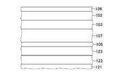
- a channel layer 102 and a barrier layer 103 made of a nitride semiconductor are formed on a first substrate 101 (first step).
- the channel layer 102 and the barrier layer 103 are grown on the first substrate 101 in this order by crystal growth in the +c-axis direction.
- the nucleation layer 104, the sacrifice layer 105, and the gate separation layer 106 are formed on the first substrate 101, and then the channel layer 102 and the barrier layer 103 are formed, and the barrier layer 103 is formed. Then, the first main bonding layer 107 and the first sub-bonding layer 108 are formed.
- the gate separation layer 106 is formed on the first substrate 101 side of the channel layer 102.
- the nucleation layer 104, the sacrifice layer 105, the gate separation layer 106, the first main junction layer 107, and the first sub junction layer 108 are also formed by crystal growth in the +c-axis direction. Since the crystal is grown in the +c-axis direction, the barrier layer 103 is formed on the channel layer 102, so that the heterojunction between the channel layer 102 and the barrier layer 103 is spontaneously about 10 13 cm ⁇ 3 . A high density sheet carrier is formed.
- the first substrate 101 is made of, for example, Al 2 O 3 (sapphire), and the plane orientation of the main surface thereof is (0001), for example.
- the first substrate 101 may be made of SiC, single crystal Si, or the like, or may be made of a material that can be used for growing a nitride semiconductor, such as GaN or AlN.
- Si capable of performing substrate removal by dry etching or Al 2 O 3 to which a known peeling technique such as laser lift-off is applicable is more preferable. It is not limited.
- the nucleation layer 104 is composed of, for example, GaN. As is well known, the nucleation layer 104 supports nucleation in the early stage of growth for crystal growth of a nitride semiconductor such as GaN on a dissimilar substrate such as Al 2 O 3 , Si, or SiC. This is a layer for obtaining high quality and flat crystals.
- the nucleation layer 104 has various names such as a low temperature buffer layer and a low temperature buffer.
- the surface of the nucleation layer 104 is a group III polar surface by adjusting the nucleation layer 104. By making the surface of the nucleation layer 104 to be a group III polar surface, the nitride semiconductor is crystal-grown thereon in the +c-axis direction. Note that the nucleation layer 104 is not limited to GaN and can be made of other nitrides such as AlN and AlON. However, when the first substrate 101 is made of GaN, the nucleation layer 104 may not be necessary.
- the sacrificial layer 105 is made of, for example, GaN.
- the sacrificial layer 105 is used for removing the first substrate 101 described later and for planarizing the surface of the semiconductor laminated structure after removing the first substrate 101. Therefore, the thickness of the sacrificial layer 105 is set appropriately in conformity with the step of removing the first substrate 101, and is, for example, 100 nm or more. Note that the sacrificial layer 105 also functions as a buffer layer of a layer that grows above the sacrificial layer 105 along with the nucleation layer 104.
- the gate separation layer 106 is made of a material having a bandgap larger than that of the channel layer 102, such as AlGaN.
- the gate separation layer 106 is typically made of AlGaN having an Al composition set to about 0.10.
- the gate separation layer 106 is formed to have a thickness of about 20 nm. Note that the gate separation layer 106 is also used as an etching stop layer for removing the sacrifice layer 105 by selective etching in a step after removing the first substrate 101 described later.
- the channel layer 102 is made of, for example, GaN.
- the barrier layer 103 is made of AlGaN.
- the thickness of the channel layer 102 and the thickness of the barrier layer 103 are determined in consideration of the desired HEMT sheet resistance and mobility, the critical film thickness of the entire epitaxially grown layer structure, and the like.
- the barrier layer 103 may be formed in contact with the channel layer 102, and a spacer layer made of, for example, AlN may be arranged between the barrier layer 103 and the channel layer 102. Further, the barrier layer 103 made of AlGaN may be configured such that the Al composition gradually changes in the direction away from the channel layer 102 from the channel layer 102 side.
- the first main junction layer 107 is made of GaN
- the first sub-junction layer 108 is made of GaN having a high resistance by being doped with C.
- the above-mentioned layers can be formed by a well-known metal organic chemical vapor deposition method.
- the layers described above are formed by molecular beam epitaxy (including gas source, RF plasma source, laser, etc.), hydride vapor phase epitaxy, sputtering, and other CVD (Chemical Vapor Deposition) methods. It is also possible to do so.
- a second substrate 121 made of a nitrogen-free semiconductor is prepared (second step).
- the second substrate 121 is made of a material that can be regrown from a material that can be doped with impurities at a higher concentration and that easily lowers resistance when forming a source region and a drain region by a regrowth process described later.
- a material that can be doped with impurities at a higher concentration and that easily lowers the resistance is, for example, a nitrogen-free III-V group compound semiconductor such as GaAs or InP.
- the second substrate 121 can also be made of Si.
- the second substrate 121 is made of high-resistance GaAs.
- the etching stopper layer 122 made of InGaAsP and the second junction layer 123 made of GaAs having high resistance are formed on the second substrate 121 by epitaxial growth.
- the second substrate 121 is attached to the barrier layer 103 side and the channel layer 102 side of the first substrate 101 (third step).
- the second bonding layer 123 of the second substrate 121 is bonded to the first sub bonding layer 108 of the first substrate 101, and the first substrate 101 and the second substrate 121 are bonded together.
- This bonding is performed by a well-known wafer bonding technique such as a surface activated bonding method, fusion by high temperature heat treatment, and atomic diffusion bonding method.
- the crystal growth temperature may become relatively high in some cases, so a bonding technique that can obtain a bonding state that can withstand this temperature is used.
- the first substrate 101 is removed, and as shown in FIG. 1D, the barrier layer 103 and the channel layer 102 are formed in this order on the second substrate 121 (fourth step).
- the etching stop layer 122, the second bonding layer 123, the first sub-bonding layer 108, the first main bonding layer 107, the barrier layer 103, the channel layer 102, and the gate separation layer are formed on the second substrate 121.
- 106, the sacrificial layer 105, and the nucleation layer 104 are formed in this order.
- the first substrate 101 is removed by peeling the first substrate 101 from the nucleation layer 104 by a known laser lift-off method. Further, the first substrate 101 can be removed by back grinding and dry etching. Note that the removal of the first substrate 101 is performed by a method that does not affect the barrier layer 103 and the channel layer 102 such that damage that causes deterioration of transistor characteristics is introduced.
- the sacrificial layer 105 is thinned. As will be described later, the sacrificial layer 105 is removed to expose the surface of the gate isolation layer 106.
- an etching process using the sacrificial layer 105 as an etching stop layer is used for removing the sacrificial layer 105.
- the sacrificial layer 105 is thinned according to the size of the etching selectivity that can be taken between the gate separation layer 106 and the sacrificial layer 105 in this etching process.
- the flatness of the surface of the sacrificial layer 105 may be transferred to the surface of the gate separation layer 106. Therefore, the sacrifice layer 105 is thinned and the surface is flattened.
- the surface of the sacrificial layer 105 is flattened and thinned by grinding and polishing the sacrificial layer 105 by well-known chemical mechanical polishing (CMP).
- CMP chemical mechanical polishing
- the thickness of the sacrificial layer 105 cut by the CMP depends on the state of the removal of the first substrate 101 in the previous step and the state of the sacrificial layer 105 after the removal of the first substrate 101.
- the sacrificial layer 105 is thickened by CMP in order to remove a portion where the flatness is impaired in the entire surface direction. Grinding and polishing of about several hundreds nm is performed.
- the sacrificial layer 105 is formed to have a thickness of 1000 nm or more, the sacrificial layer 105 will not be completely lost even if it is thinned by the above-described CMP. As shown in FIG. 1E, the thinned sacrificial layer 105a remains on the gate isolation layer 106 by the above-described planarization and thinning process.
- the thinned sacrificial layer 105a is removed to expose the surface of the gate isolation layer 106 as shown in FIG. 1F. Since the sacrificial layer 105a is made of GaN and the gate separation layer 106 is made of AlGaN, the gate separation layer 106 is used as an etching stop layer by a dry etching process using chlorine gas, nitrogen gas, or oxygen gas, for example. It is possible to remove the sacrificial layer 105a.
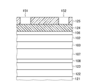
- a silicon oxide layer 124 is formed on the gate isolation layer 106, and a mask layer 125 having openings 151 and 152 is formed on the silicon oxide layer 124.
- the silicon oxide layer 124 is formed by depositing silicon oxide by a well-known deposition method.
- a positive photoresist material is applied on the silicon oxide layer 124 to form a coating layer.
- the formed coating layer is patterned by a known lithography technique to form the mask layer 125 having the openings 151 and 152.
- the opening 151 and the opening 152 are formed in the source region and the drain region.
- the silicon oxide layer 124 is dry-etched using the mask layer 125 as a mask, so that openings are formed in the silicon oxide layer 124 at the same positions as the openings 151 and 152 of the mask layer 125.
- each layer on the second substrate 121 side (lower side) of the silicon oxide layer 124 is removed by etching using the silicon oxide layer 124 having two openings as a mask.
- the first groove 153 and the second groove 153 penetrating the barrier layer 103 and the channel layer 102 are sandwiched between the barrier layer 103 and the channel layer 102 with a region for forming a gate electrode therebetween.
- the groove 154 is formed (fifth step).
- etching is performed up to the middle of the second bonding layer 123 in the thickness direction.
- the etching stopper layer 122 made of InGaAsP is formed.
- the second bonding layer 123 made of GaAs is selectively etched. By this etching, the surface of the etching stopper layer 122 is exposed at the bottoms of the first groove 153 and the second groove 154.
- the first regrowth layer 109 and the second regrowth layer made of GaAs having high resistance are formed on the surface of the etching stopper layer 122 exposed at the bottoms of the first groove 153 and the second groove 154.
- the first regrowth layer 109 and the second regrowth layer 110 are formed at a height (thickness) reaching the middle of the barrier layer 103 in the thickness direction.
- the silicon oxide layer 124 as a selective growth mask, crystal growth of high-resistance GaAs is performed by a known metal organic chemical vapor deposition method or molecular beam epitaxy method.
- Layer 110 can be formed.
- the first regrowth layer 109 and the second regrowth layer 110 made of GaAs are formed by epitaxial growth on the etching stopper layer 122 made of InGaAsP. Since the etching stopper layer 122 is formed by epitaxial growth on the second substrate 121 made of GaAs, high crystal quality is maintained. In this way, the first regrowth layer 109 and the second regrowth layer 110 formed by epitaxial growth on the etching stopper layer 122 maintaining a high crystal quality also maintain a high crystal quality.
- the source region 111 and the drain region 112 which are in contact with the channel layer 102 are formed in the first groove 153 and the second groove 154 (sixth step), and the ohmic contact is formed on the source region 111.
- a source electrode 113 for connection is formed, and a drain electrode 114 for ohmic connection is formed on the drain region 112 (seventh step).
- N-type InGaAs is a semiconductor containing no impurities and containing no nitrogen.
- n-type InGaAs doped with Si as a dopant at a high concentration of 1e10 19 cm ⁇ 3 or more is used by a known metal organic chemical vapor deposition method or molecular beam epitaxy method using the silicon oxide layer 124 as a selective growth mask.
- the source region 111 and the drain region 112 are formed by crystal growth.
- the source region 111 and the drain region 112 are formed so that their upper surfaces are located above the gate isolation layer 106.
- the first regrowth layer 109 and the second regrowth layer 110 maintain high crystal quality
- the source region 111 and the drain region 112 epitaxially grown thereon also maintain high crystal quality.
- the source region 111 and the drain region 112 made of InGaAs can have a higher impurity concentration than a nitride semiconductor, and can have a lower resistance than a nitride semiconductor. ..
- the source electrode 113 and the drain electrode 114 are formed by depositing an electrode material (metal) capable of forming an ohmic contact by a known vapor deposition method or sputtering method.
- An electrode material capable of forming an ohmic contact is, for example, Ti/Pt/Au. This electrode material can realize extremely low contact resistance with respect to InGaAs, for example, even in a non-alloyed state. Further, in the non-alloyed state, no ohmic contact is formed on the GaN layer (channel layer 102) via the AlGaN layer (gate separation layer 106).
- the source electrode 113 and the drain electrode 114 can be formed by depositing the above electrode material to form an electrode material layer and then patterning the electrode material layer by a known lithography technique and etching technique. Further, the source electrode 113 and the drain electrode 114 can be formed by a well-known lift-off method.
- a gate electrode 115 is formed on the barrier layer 103 and the channel layer 102 between the source electrode 113 and the drain electrode 114 (eighth step).
- the gate electrode 115 that forms a Schottky connection is formed on the gate isolation layer 106.
- the gate electrode 115 can be composed of a gate metal material such as Ni/Au. After depositing the gate metal material to form the gate metal material layer, the gate electrode 115 can be formed by patterning the gate metal material by a known lithography technique and etching technique.
- the gate isolation layer 106 made of a material having a bandgap larger than the bandgap of the channel layer 102 is formed on the channel layer 102, and the Schottky-connected gate electrode is formed on the gate isolation layer 106. 115 are formed.
- the source electrode 113, the drain electrode 114, and the channel layer 102 are contacted with each other through the source region 111 and the drain region 112, which have lower resistance than the nitride semiconductor. Therefore, the contact resistance of the source/drain electrodes of the GaN-based HEMT can be reduced as compared with the conventional technique. As a result, according to the present invention, it is possible to further expand the high frequency characteristics of the GaN-based HEMT and broaden the band.
- Embodiment 2 Next, a method for manufacturing a transistor in Embodiment 2 of the present invention will be described with reference to FIGS. 2A to 2I.
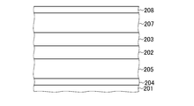
- a barrier layer 202 and a channel layer 203 made of a nitride semiconductor are formed on a first substrate 201 (first step).
- the barrier layer 202 and the channel layer 203 are grown in this order on the first substrate 201 by crystal growth in the ⁇ c-axis direction.
- the nucleation layer 204 and the sacrificial layer 205 are formed on the first substrate 201, and then the barrier layer 202 and the channel layer 203 are formed, and the first main layer is formed on the barrier layer 202.
- the bonding layer 207 and the first sub bonding layer 208 are formed.
- the nucleation layer 204, the sacrificial layer 205, the first main bonding layer 207, and the first sub bonding layer 208 are also formed by crystal growth in the ⁇ c axis direction. Since the crystal is grown in the ⁇ c-axis direction, by forming the channel layer 203 on the barrier layer 202, the heterojunction between the barrier layer 202 and the channel layer 203 spontaneously forms about 10 13 cm ⁇ 3. A high density sheet carrier is formed.
- the first substrate 201 is made of, for example, Al 2 O 3, and the plane orientation of the main surface is (0001), for example.
- the first substrate 201 is made of a material that can be used for growing a nitride semiconductor such as GaN.
- Si capable of performing substrate removal by dry etching, or Al 2 O 3 to which a known peeling technique such as laser lift-off is applicable is more preferable. It is not limited.
- the nucleation layer 204 is composed of, for example, GaN. As is well known, the nucleation layer 204 supports nucleation in the early stage of growth for crystal growth of a nitride semiconductor such as GaN on a dissimilar substrate such as Al 2 O 3 or Si or SiC. This is a layer for obtaining high quality and flat crystals.
- the nucleation layer 204 has various names such as a low temperature buffer layer and a low temperature buffer.
- a nucleation layer 204 whose surface is a group V polar surface can be formed.
- the nitride semiconductor will grow on it in the ⁇ c-axis direction.
- the nucleation layer 204 is not limited to GaN, but can be made of another nitride such as AlN. However, when the first substrate 201 is made of GaN, the nucleation layer 204 is not necessary.
- the sacrificial layer 205 is made of, for example, GaN.
- the sacrificial layer 205 is used for removing the first substrate 201 described below and for planarizing the surface of the semiconductor laminated structure after removing the first substrate 201. Therefore, the thickness of the sacrificial layer 205 is appropriately set in conformity with the step of removing the first substrate 201, and is, for example, 100 nm or more. Note that the sacrificial layer 205 also functions as a buffer layer of a layer that grows above the sacrificial layer 205 along with the nucleation layer 204.
- the channel layer 203 is made of, for example, GaN.
- the barrier layer 202 is made of AlGaN.
- the thickness of the channel layer 203 and the thickness of the barrier layer 202 are determined in consideration of the desired HEMT sheet resistance and mobility, the critical film thickness of the entire epitaxially grown layer structure, and the like.
- the barrier layer 202 may be formed in contact with the channel layer 203, and a spacer layer made of, for example, AlN can be arranged between the barrier layer 202 and the channel layer 203. Further, the barrier layer 202 made of AlGaN may be configured such that the Al composition gradually changes from the channel layer 203 side to the direction away from the channel layer 203.
- the first main junction layer 207 is made of GaN
- the first sub-junction layer 208 is made of GaN doped with C to have high resistance.
- a second substrate 221 made of a nitrogen-free semiconductor is prepared (second step).
- the second substrate 221 is made of a material that can be regrown with a material that can be doped with impurities at a higher concentration and that easily lowers resistance when the source region and the drain region are formed by a regrowth process described later.
- a material which can be doped with impurities at a higher concentration and whose resistance is easily reduced is, for example, a III-V group compound semiconductor containing no nitrogen such as GaAs.
- the second substrate 221 is made of high-resistance GaAs.
- the etching stopper layer 222 made of InGaAsP and the second junction layer 223 made of high-resistance GaAs are formed on the second substrate 221 by epitaxial growth.
- the second substrate 221 is attached to the barrier layer 202 and the channel layer 203 side of the first substrate 201 (third step). Also in the second embodiment, the second bonding layer 223 of the second substrate 221 is bonded to the first sub bonding layer 208 of the first substrate 201, and the first substrate 201 and the second substrate 221 are bonded together. This bonding is the same as in the first embodiment described above.
- the first substrate 201 is removed, and as shown in FIG. 2D, the channel layer 203 and the barrier layer 202 are formed in this order on the second substrate 221.
- the etching stop layer 222, the second bonding layer 223, the first sub-bonding layer 208, the first main bonding layer 207, the channel layer 203, the barrier layer 202, and the sacrificial layer 205 are formed on the second substrate 221.
- the nucleation layer 204 is in a state of being formed in this order.
- the barrier layer 202 is formed on the channel layer 203 when viewed from the second substrate 221.
- the sacrificial layer 205 is thinned.
- the sacrificial layer 205 will be removed to expose the surface of the barrier layer 202 as described below.
- an etching process using the sacrificial layer 205 as an etching stop layer is used for removing the sacrificial layer 205.
- the sacrificial layer 205 is thinned in accordance with the etching selection ratio that can be taken between the barrier layer 202 and the sacrificial layer 205 in this etching process.
- the flatness of the surface of the sacrificial layer 205 may be transferred to the surface of the barrier layer 202. Therefore, the sacrifice layer 205 is thinned and the surface is flattened.
- the surface of the sacrificial layer 205 is flattened and thinned by grinding and polishing the sacrificial layer 205 by CMP.
- the thickness of the sacrificial layer 205 cut by the CMP depends on the state of the removal of the first substrate 201 in the previous step and the state of the sacrificial layer 205 after the removal of the first substrate 201.
- the thickness of the sacrificial layer 205 is reduced by CMP in order to remove a portion where the flatness is impaired in the entire surface direction. Grinding and polishing of about several hundreds nm is performed. If the sacrifice layer 205 is formed to have a thickness of 1000 nm or more, the sacrifice layer 205 will not be completely lost even if it is thinned by the above-mentioned CMP.
- the thinned sacrificial layer 205 is removed to expose the surface of the barrier layer 202 as shown in FIG. 2E. Since the sacrificial layer 205 is made of GaN and the barrier layer 202 is made of AlGaN, the sacrificial layer 205 is used as an etching stop layer by a dry etching process using chlorine gas, nitrogen gas, or oxygen gas, for example. Removal of layer 205 is possible.
- a silicon oxide mask 224 having openings in the source region and the drain region is formed on the barrier layer 202.
- the silicon oxide mask 224 is similar to the formation of the silicon oxide layer 124 described with reference to FIG. 1G.
- each layer on the second substrate 221 side (lower side) of the silicon oxide mask 224 is removed by etching.
- the first groove 251 and the second groove 252 which penetrate the barrier layer 202 and the channel layer 203 are formed in the barrier layer 202 and the channel layer 203 with the region for forming the gate electrode interposed therebetween (the first 5 steps).
- RIE reactive ion etching
- ICP inductively coupled plasma
- Cl 2 chlorine-based gas
- etching is performed up to the middle of the second bonding layer 223 in the thickness direction.
- the etching stopper layer 222 made of InGaAsP is formed.
- the second bonding layer 223 made of GaAs is selectively etched. By this etching, the surface of the etching stop layer 222 is exposed at the bottoms of the first groove 251 and the second groove 252.
- the first regrowth layer 209 and the second regrowth layer made of GaAs having high resistance are formed on the surface of the etching stopper layer 222 exposed at the bottoms of the first groove 251 and the second groove 252, the first regrowth layer 209 and the second regrowth layer made of GaAs having high resistance are formed.
- the first regrowth layer 209 and the second regrowth layer 210 are formed at a height (thickness) that reaches the middle of the channel layer 203 in the thickness direction.
- the first regrowth layer 209 and the second regrowth layer 210 can also be formed to have a thickness that reaches the middle of the first main bonding layer 207 in the thickness direction.
- the channel layer 203 is exposed on the side surfaces of the first groove 251 and the second groove 252 on the first regrowth layer 209 and the second regrowth layer 210.
- the silicon oxide mask 224 made of silicon oxide as a selective growth mask, crystal growth of high-resistivity GaAs is performed by a known metal-organic vapor phase epitaxy method or molecular beam epitaxy method.
- the second regrowth layer 210 can be formed.
- the first regrowth layer 209 and the second regrowth layer 210 made of GaAs are formed by epitaxial growth on the etching stopper layer 222 made of InGaAsP. Since the etching stop layer 222 is formed by epitaxial growth on the second substrate 221 made of GaAs, high crystal quality is maintained. In this way, the first regrowth layer 209 and the second regrowth layer 210 formed by epitaxial growth on the etching stopper layer 222 maintaining high crystal quality also maintain high crystal quality.
- a source region 211 and a drain region 212 which are in contact with the channel layer 203 are formed in the first groove 251 and the second groove 252 (sixth step), and the ohmic contact is formed on the source region 211.
- a source electrode 213 for connection is formed, and a drain electrode 214 for ohmic connection is formed on the drain region 212 (seventh step).
- N-type InGaAs is a semiconductor containing no impurities and containing no nitrogen.
- n-type InGaAs doped with Si as a dopant at a high concentration of 1e10 19 cm ⁇ 3 or more is used by a known metal organic chemical vapor deposition method or molecular beam epitaxy method using the silicon oxide mask 224 as a selective growth mask.
- the source region 211 and the drain region 212 are formed by crystal growth.
- the source region 211 and the drain region 212 are formed so that their upper surfaces are located above the barrier layer 202.
- the first regrowth layer 209 and the second regrowth layer 210 maintain high crystal quality, and the epitaxially grown source region 211 and drain region 212 also maintain high crystal quality. .. Further, the source region 211 and the drain region 212 made of InGaAs can have a higher impurity concentration than the nitride semiconductor, and can have a lower resistance than the nitride semiconductor. ..
- a source electrode 213 and a drain electrode 214 are formed by depositing an electrode material (metal) capable of forming an ohmic contact by a known vapor deposition method or sputtering method.
- An electrode material capable of forming an ohmic contact is, for example, Ti/Pt/Au. This electrode material can realize extremely low contact resistance with respect to InGaAs, for example, even in a non-alloyed state. Further, in the non-alloyed state, no ohmic contact is formed on the GaN layer (channel layer 203) via the AlGaN layer (barrier layer 202).
- the source electrode 213 and the drain electrode 214 can be formed by depositing the above electrode material to form an electrode material layer and then patterning the electrode material layer by a known lithography technique and etching technique. Further, the source electrode 213 and the drain electrode 214 can be formed by a well-known lift-off method.
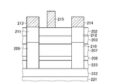
- a gate electrode 215 is formed on the channel layer 203 and the barrier layer 202 between the source electrode 213 and the drain electrode 214 (eighth step).
- the gate electrode 215 that forms a Schottky connection is formed on the barrier layer 202.
- the gate electrode 215 can be composed of a gate metal material such as Ni/Au. After depositing the gate metal material to form the gate metal material layer, the gate electrode 215 can be formed by patterning the gate metal material by a known lithography technique and etching technique.
- the source electrode 213, the drain electrode 214, and the channel layer 203 are in contact with each other through the source region 211 and the drain region 212, which have lower resistance than the nitride semiconductor. Therefore, the contact resistance of the source/drain electrodes of the GaN-based HEMT can be reduced as compared with the conventional technique. As a result, according to the present invention, it is possible to further expand the high frequency characteristics of the GaN-based HEMT and broaden the band.
- a barrier layer and a channel layer made of a nitride semiconductor are crystal-grown in the c-axis direction, and a second substrate made of a semiconductor containing no nitrogen is bonded to the first substrate.
- a first groove and a second groove penetrating the barrier layer and the channel layer were formed, and a source region and a drain region in contact with the channel layer were formed in the first groove and the second groove.
- the first substrate when the first substrate is made of Si, the first substrate can be removed by dry etching, and can be selectively removed from the GaN-based material layer such as the nucleation layer. Further, when the first substrate is made of SiC or GaN, a layer of a GaN-based material can be epitaxially grown and a high quality crystal can be easily obtained. However, from the viewpoint of removing the first substrate, a buffer layer or the like is used. It requires technical innovation. Of course, even when the first substrate is made of SiC or GaN, it can be sufficiently applied as long as the first substrate can be removed over a wide range without introducing damage to the channel layer or the barrier layer. Is.
- nucleation layers such as AlN, AlGaN, and AlON can be used as long as there is no problem in the step of removing the first substrate and the characteristics of HEMT. Can also be formed.
- GaN is used as the sacrificial layer has been illustrated, but for the purpose of further improving the crystal quality, for example, a method of growing GaN under different growth conditions over a plurality of stages can be used.
- the sacrificial layer it is also possible to use a GaN layer formed by a growth method using a mask that promotes lateral growth.
- the etching stopper layer is made of AlGaN
- other materials can be used as long as the purpose is to stop etching.
- GaN is used as the sacrificial layer
- using an Al-containing layer as an etching stop layer is superior from the viewpoint of obtaining a selection ratio by a method such as dry etching or thermal decomposition.
- the purpose is essentially to expose the channel layer or barrier layer to a processable state or to bring it close to a region close to the surface, and if this can be achieved without using an etching stop layer, as described above, It is not necessary to introduce an etch stop layer.
- the channel layer is made of GaN and the barrier layer is made of AlGaN, but the present invention is not limited to this.
- the channel layer may be composed of InGaN, InN, AlGaN, or the channel layer may have a heterostructure such as GaN/InGaN.
- the barrier layer may be made of InAlN, InAlGaN, AlN, or GaN, or may have a multi-layer structure by combining these materials.
- the HEMT is described as an example, but the present invention can be applied to other transistors, photodiodes, modulators, and the like.
- C was used as a dopant to increase the resistance of the nitride semiconductor, it is also possible to use Zn or Fe as a dopant, for example. Further, if the damage introduced by the bonding is within the allowable range of the influence on the device characteristics, it is not necessary to use the bonding layer.
- the etching stop layer may be made of a material containing P such as InGaAsP or InGaP or a material containing Al such as AlGaAs in order to stop the etching by wet etching. it can.
- the second substrate is made of high resistance InP
- a layer containing As such as InAlAs or InGaAs can be used as the etching stop layer.
- high resistance GaAs, high resistance InP, etc. can be selected according to the second substrate.
Landscapes
- Junction Field-Effect Transistors (AREA)
- Chemical & Material Sciences (AREA)
- Crystallography & Structural Chemistry (AREA)
- Electrodes Of Semiconductors (AREA)
- Recrystallisation Techniques (AREA)
Abstract
第1溝(153)および第2溝(154)の底部に露出したエッチング停止層(122)の表面に、高抵抗なGaAsからなる第1再成長層(109),第2再成長層(110)を再成長させ、n型のInGaAsを第1再成長層(109),第2再成長層(110)の上に再成長させることで、チャネル層(102)に接触するソース領域(111)、ドレイン領域(112)を、第1溝(153)および第2溝(154)に形成する。
Description
本発明は、トランジスタの作製方法に関し、より具体的には、窒化物半導体とGaAsやInPなどの半導体とから構成したトランジスタの作製方法に関する。
窒化ガリウム(GaN)、窒化アルミニウム(AlN)またはこれらの混晶材料であるAlGaNやInAlGaNなどの窒化物半導体は、GaAsやSiなどの半導体材料と比較して、バンドギャップが大きく、高い絶縁破壊電界強度を有する。このような特徴から、トランジスタなどの電子デバイスを窒化物半導体から構成すると、高い耐圧特性を実現することができる。また、窒化物半導体は、六方晶の結晶構造を有しており、c軸方向に分極を有する。この分極の効果によって、例えば、AlGaNとGaNとのヘテロ接合を形成することで、自発的に、1013cm-3程度の高密度のシートキャリア(2次元電子ガス)が形成される。このシートキャリアにより、よく知られた高電子移動度トランジスタ(HEMT)が実現できる。
ここで、GaN系の窒化物半導体を用いたHEMTについて図3を参照して説明する。このHEMTは、まず、基板301の上、エピタキシャル成長によって形成されたバッファ層302、チャネル層303,バリア層304が順次に積層されている。基板301は、サファイア、Si、SiC、および単結晶GaNから構成できる。また、チャネル層303は、GaNから構成され、バリア層304は、AlGaNから構成されている。
バリア層304とチャネル層303とは、分極の大きさが異なり、この結果、バリア層304とチャネル層303との界面のチャネル層303の側に、シートキャリアが形成される。この半導体積層構造に対して、よく知られた半導体製造プロセスにより、バリア層304の上に、ゲート電極311を形成し、ゲート電極311を挾んでソース電極312,ドレイン電極313を形成する。ゲート電極311は、いわゆるショットキー接続とし、ソース電極312,ドレイン電極313は、チャネル層303にオーミック接続させる。
なお、上述したHEMTは、基板301の上に+c軸方向に窒化物半導体を結晶成長することで各層を形成しており、この場合、チャネル層303の上にバリア層304を配置することで、バリア層304とチャネル層303との界面のチャネル層303の側に、シートキャリアが形成される。これに対し、-c軸方向に窒化物半導体を結晶成長する場合、バリア層の上にチャネル層を配置することで、これらの界面のチャネル層の側に、シートキャリアが形成される。ここで、基板からみて、バリア層の上にもチャネル層が配置される場合、チャネル層の上に直接ゲート電極を形成すると、ゲートリークの増大などが引き起こされ所望の特性を引き出すことができない。このため、この場合は、チャネル層の上に、例えば、チャネル層のバンドギャップより大きいバンドギャップを有する窒化物半導体層を形成し、この窒化物半導体層の上に、ショットキー接続するゲート電極を形成する。例えば、チャネル層をGaNから構成した場合、窒化物半導体層は、AlGaNから構成する。
上述したGaN系の窒化物半導体を用いたHEMT(GaN系HEMT)は、数GHz以上の高周波かつ数百Wの高出力が要求される無線通信用途において、既に実現・実用化されている。今後、さらなる無線通信容量の拡大に向けて、数十から数百GHz程度まで高周波特性を向上させたGaN系HEMTが必要となる。GaN系HEMTの高周波特性向上のためには、ソース・ドレイン領域のコンタクト抵抗の低減が重要である。
ところで、GaNは、ワイドギャップ材料であるため、高い絶縁破壊電界強度を有するが、GaNの層の上にオーミック電極を形成した際のコンタクト抵抗の低減が困難である。これは、GaN自体の抵抗が高く、また、高濃度にドーピングしたとしてもコンタクト抵抗の低減化に制限があることに原因がある。また、上述したGaN系HEMTでは、GaNよりもさらにバンドギャップが大きく抵抗の高いAlGaNなどの層を介し、各電極とのコンタクトを形成する必要があるため、さらにコンタクト抵抗が高くなってしまう。
上述したGaN系HEMTにおける、ソース電極、ドレイン電極とチャネル層との間のコンタクト抵抗の低減手段の1つに、ソース電極・ドレイン電極と接続するためのソース・ドレイン領域の再成長が挙げられる。GaN系HEMTは、AlGaNなどの層を介してGaNからなるチャネル層にオーミックコンタクトを形成するため、AlGaNの高い抵抗によってコンタクト抵抗が制限されてしまう。これを回避するために、例えばソース・ドレイン領域に高濃度ドープされたGaNを再成長によって形成することで、コンタクト抵抗を低減する技術がある(非特許文献1)。
この技術により、上述したコンタクト抵抗は、0.026Ω*mmまで低減される。このコンタクト抵抗の値は、最大発振周波数fmax>1THzの特性を有するInAsチャネルHEMTのコンタクト抵抗40mΩ*mmに匹敵する(非特許文献2)。しかし、コンタクト抵抗の値は小さくできるが、GaN系HEMTの性能は、fmax=518GHzと制限されている。
さらにコンタクト抵抗の低減化をして、GaN系HEMTを広帯域化する手段として、GaAsやInP、InGaAs、InAsといったGaN系材料よりも、高濃度ドープにより低抵抗化しやすい材料を再成長する技術が考えられる。例えば、非特許文献3においては、GaN上にGaAsを成長させる試みが報告されている。GaAsは、Siをドーピングしてn型化することができる。実際、非特許文献3においては、1019~1020cm-3まで高濃度ドープしたp型GaAs層を、GaN層の上に成長することに成功している。しかし、GaAsとGaNとは結晶構造が異なり、また2つの層の界面における面方向の格子不整合が極めて大きいため、このような構造の異なる材料に対するヘテロ成長は難しく、結晶品質の低下や平坦性の悪化などの問題が発生する。
K. Shinohara et al., "Self-Aligned-Gate GaN-HEMTs with Heavily-Doped n+-GaN Ohmic Contacts to 2DEG", IEEE International Electron Devices Meeting, 13384135, 2012.
X. Mei et al., "First Demonstration of Amplification at 1 THz Using 25-nm InP High Electron Mobility Transistor Process", IEEE Electron Device Letters, vol. 36, no. 4, pp. 327-329, 2015.
G. T. Dang et al., "p-Ohmic contact resistance for GaAs(C)/GaN(Mg)", Solid-State Electronics, vol. 44, pp. 105-109, 2000.
GaN系HEMTのさらなる高周波動作帯域の拡大に向けては、ソース・ドレイン電極のオーミックコンタクト抵抗の低減が必須である。しかし、前述したように、GaNはワイドギャップ材料であるため、コンタクト抵抗の低減化には制限がある。コンタクト抵抗を低減するためには、例えば、GaAsなど、高濃度ドープが可能な半導体材料を、ソース・ドレイン領域に再成長することが考えられるが、異種材料への成長であるため、大きな格子不整合・結晶構造の違いに起因して、高品質な結晶が得られにくいなどの問題がある。
上述したように、従来では、GaN系HEMTなどの窒化物半導体を用いたトランジスタのソース・ドレイン電極のコンタクト抵抗低減に制限があり、GaN系HEMTのさらなる高周波動作帯域の拡大を阻害しているという問題があった。
本発明は、以上のような問題点を解消するためになされたものであり、窒化物半導体を用いたトランジスタのソース・ドレイン電極のコンタクト抵抗がより低減できるようにすることを目的とする。
本発明に係るトランジスタの作製方法は、第1基板の上に、窒化物半導体からなるバリア層およびチャネル層を、c軸方向に結晶成長する第1工程と、窒素を含まない半導体からなる第2基板を用意する第2工程と、第1基板のバリア層およびチャネル層の側に第2基板を貼り合わせる第3工程と、第1基板を除去し、第2基板の上に、バリア層およびチャネル層が形成された状態とする第4工程と、第1基板を除去した後で、バリア層およびチャネル層に、ゲート電極を形成する領域を挟んで、バリア層およびチャネル層を貫通する第1溝および第2溝を形成する第5工程と、第1溝の底面および第2溝の底面の側より、不純物を導入した窒素を含まない半導体を再成長させることで、チャネル層に接触するソース領域、ドレイン領域を、第1溝および第2溝に形成する第6工程と、ソース領域の上にオーミック接続するソース電極を形成し、ドレイン領域の上にオーミック接続するドレイン電極を形成する第7工程と、ソース電極とドレイン電極との間のバリア層およびチャネル層の上に、ゲート電極を形成する第8工程とを備える。
上記トランジスタの作製方法の一構成例において、第1工程は、バリア層の上に第1接合層を形成し、第2工程は、第2基板の上に第2接合層を形成し、第3工程では、第1接合層と第2接合層とを向かい合わせた状態で第1基板と第2基板とを貼り合わせる。
上記トランジスタの作製方法の一構成例において、第4工程では、バリア層の一部とともに第1基板を除去する。
上記トランジスタの作製方法の一構成例において、第1工程は、第1基板の上に犠牲層を介してバリア層およびチャネル層を形成し、第4工程では、犠牲層の一部とともに第1基板を除去する。
上記トランジスタの作製方法の一構成例において、第1工程では、+c軸方向に結晶成長することで、チャネル層およびバリア層を、これらの順に第1基板の上に成長し、加えて、チャネル層の第1基板の側に、チャネル層のバンドギャップより大きいバンドギャップを有する材料から構成されたゲート分離層を、チャネル層に接して形成し、第8工程では、ゲート分離層の上にゲート電極を形成する。
上記トランジスタの作製方法の一構成例において、第1工程では、-c軸方向に結晶成長することで、バリア層およびチャネル層を、これらの順に第1基板の上に成長し、第8工程では、バリア層の上にゲート電極を形成する。
上記トランジスタの作製方法の一構成例において、第1基板は、サファイア、Si、SiC、GaN、AlNのいずれかから構成され、第2基板は、GaAs、InP、Siのいずれかから構成されている。
上記トランジスタの作製方法の一構成例において、チャネル層は、GaN、InGaN、InN、AlGaNのいずれかまたはこれらの積層構造から構成され、バリア層は、AlGaN、InAlN、InAlGaN、AlN、GaNのいずれかまたはこれらの積層構造によって構成されている。
以上説明したように、本発明では、窒化物半導体からなるバリア層およびチャネル層を、c軸方向に結晶成長した第1基板に、窒素を含まない半導体からなる第2基板を貼り合わせ、第1基板を除去してから、バリア層およびチャネル層を貫通する第1溝および第2溝を形成し、チャネル層に接触するソース領域、ドレイン領域を、第1溝および第2溝に形成した。この結果、本発明によれば、窒化物半導体を用いたトランジスタのソース・ドレイン電極のコンタクト抵抗がより低減できるという優れた効果が得られる。
以下、本発明の実施の形態に係るトランジスタの作製方法について説明する。
[実施の形態1]
はじめに、本発明の実施の形態1におけるトランジスタの作製方法について、図1A~図1Kを参照して説明する。
はじめに、本発明の実施の形態1におけるトランジスタの作製方法について、図1A~図1Kを参照して説明する。
まず、図1Aに示すように、第1基板101の上に窒化物半導体からなるチャネル層102,バリア層103を形成する(第1工程)。実施の形態1では、+c軸方向に結晶成長することで、チャネル層102およびバリア層103を、これらの順に第1基板101の上に成長する。また、実施の形態1では、第1基板101の上に、核形成層104、犠牲層105、ゲート分離層106を形成してからチャネル層102,バリア層103を形成し、バリア層103の上に、第1主接合層107、第1副接合層108を形成する。実施の形態1においては、ゲート分離層106を、チャネル層102の第1基板101の側に形成する。
なお、核形成層104、犠牲層105、ゲート分離層106、第1主接合層107、第1副接合層108も、+c軸方向に結晶成長することで形成する。+c軸方向に結晶成長しているので、チャネル層102の上にバリア層103を形成することで、チャネル層102とバリア層103とのヘテロ接合に、自発的に、1013cm-3程度の高密度のシートキャリアが形成される。
第1基板101は、例えば、Al2O3(サファイア)から構成し、例えば、主表面の面方位を(0001)とする。なお、第1基板101は、SiCや単結晶のSiなどから構成することもでき、GaN、AlNなどの窒化物半導体の成長に用いることができる材料から構成することもできる。後述するように、第1基板101は除去するため、例えば、ドライエッチングによる基板除去が実施可能なSi、またはレーザリフトオフなどの公知の剥離技術が適用できるAl2O3がよりよいが、これらに限るものではない。
核形成層104は、例えば、GaNから構成する。核形成層104は、よく知られているように、Al2O3やSi、SiCなどの異種基板の上に、GaNなどの窒化物半導体を結晶成長するために、成長初期の核形成を支援し高品質かつ平坦な結晶を得るための層である。核形成層104は、低温緩衝層や低温バッファなど様々な呼称が存在する。また、核形成層104を調整することにより、核形成層104の表面をIII族極性面とする。核形成層104の表面をIII族極性面とすることで、この上に、窒化物半導体が+c軸方向に結晶成長するようになる。なお、核形成層104は、GaNに限らず、AlN、AlONなどの他の窒化物から構成することも可能である。ただし、第1基板101をGaNから構成する場合、核形成層104は必要ない場合もある。
犠牲層105は、例えば、GaNから構成する。犠牲層105は、後述する第1基板101の除去のため、また、第1基板101を除去した後に、半導体積層構造の表面平坦化に用いる。このため、犠牲層105の厚さは、第1基板101の除去の工程に適合させて、適宜に設定し、例えば、100nm以上とする。なお、犠牲層105は、核形成層104とともに、犠牲層105より上に結晶成長する層のバッファ層としても機能する。
ゲート分離層106は、例えば、AlGaNなどの、チャネル層102のバンドギャップより大きいバンドギャップを有する材料から構成する。ゲート分離層106は、典型的には、Al組成を0.10程度に設定したAlGaNから構成する。また、ゲート分離層106は、厚さ20nm程度に形成する。なお、ゲート分離層106は、後述する第1基板101の除去をした後の工程において、選択エッチングによって犠牲層105を除去するための、エッチング停止層としても用いる。
チャネル層102は、例えば、GaNから構成する。また、バリア層103は、AlGaNから構成する。チャネル層102の厚さおよびバリア層103の厚さは、所望とするHEMTのシート抵抗および移動度、またエピタキシャル成長する層構造全体の臨界膜厚などを考慮して決定する。バリア層103は、チャネル層102に接して形成してもよく、また、チャネル層102との間に、例えばAlNなどから構成したスペーサ層を配置してもよい。また、AlGaNから構成するバリア層103は、例えば、Al組成が、チャネル層102の側よりチャネル層102より離れる方向に、徐々に変化する構成とすることも可能である。
第1主接合層107は、GaNから構成し、第1副接合層108は、Cをドープして高抵抗化したGaNから構成する。このように、複数の層から接合層を構成することで、後述する接合工程における結晶欠陥の、チャネル層102,バリア層103への導入を抑制することが可能となる。
上述した各層は、よく知られた有機金属気相成長法により形成することができる。また、上述した各層は、分子線エピタキシ(ガスソース、RFプラズマソース、レーザなどの分類があるがいずれでもよい)、ハイドライド気相成長法、スパッタ法、その他CVD(Chemical Vapor Deposition)法などによって形成することも可能である。
次に、図1Bに示すように、窒素を含まない半導体からなる第2基板121を用意する(第2工程)。第2基板121は、後述する再成長工程によって、ソース領域およびドレイン領域を形成する際に、不純物がより高濃度にドープ可能で低抵抗化しやすい材料を再成長可能な材料から構成する。不純物がより高濃度にドープ可能で低抵抗化しやすい材料は、例えば、GaAs、InPなどの窒素を含まないIII-V族化合物半導体である。また、第2基板121は、Siから構成することもできる。実施の形態1では、第2基板121を、高抵抗なGaAsから構成する。
なお、実施の形態1では、第2基板121の上に、エピタキシャル成長により、InGaAsPからなるエッチング停止層122形成し、高抵抗なGaAsからなる第2接合層123を形成する。
次に、図1Cに示すように、第1基板101のバリア層103およびチャネル層102の側に、第2基板121を貼り合わせる(第3工程)。実施の形態1では、第1基板101の第1副接合層108に、第2基板121の第2接合層123を接合させ、第1基板101と第2基板121とを貼り合わせる。この貼り合わせは、例えば、表面活性化接合法、高温熱処理による融着、原子拡散接合法などの、よく知られたウェハ接合技術により実施する。なお、後述するソース領域・ドレイン領域を再成長では、結晶成長温度が比較的高くなる場合もあるため、この温度に耐えうる接合状態が得られる接合技術を用いる。
次に、第1基板101を除去し、図1Dに示すように、第2基板121の上に、バリア層103、チャネル層102が、これらの順に形成された状態とする(第4工程)。実施の形態1では、第2基板121の上に、エッチング停止層122、第2接合層123、第1副接合層108、第1主接合層107、バリア層103、チャネル層102、ゲート分離層106、犠牲層105、核形成層104が、これらの順に形成された状態となる。
例えば、公知のレーザリフトオフ法により第1基板101を核形成層104より剥離することで、第1基板101を除去する。また、バックグラインドおよびドライエッチングによって、第1基板101を削りとることも可能である。なお、第1基板101の除去は、バリア層103、チャネル層102に、トランジスタの特性劣化が引き起こされる損傷が導入されるなどの影響がない方法によって実施する。
次に、犠牲層105を薄層化する。後述するようにゲート分離層106の表面を露出するために、犠牲層105を除去することになる。犠牲層105の除去では、例えば、犠牲層105をエッチング停止層としたエッチング処理を用いる。このエッチング処理における、ゲート分離層106と犠牲層105との間で取り得るエッチング選択比の大きさに合わせ、犠牲層105を薄層化しておく。また、上記エッチング処理による犠牲層105の除去では、犠牲層105の表面の平坦性が、ゲート分離層106の表面に転写される場合がある。このため、犠牲層105は、薄層化するとともに、表面を平坦化しておく。
例えば、よく知られた化学機械研磨(CMP)により、犠牲層105を研削研磨することで、犠牲層105の表面を平坦化するとともに薄層化する。このCMPによって削る犠牲層105の厚さは、前工程の第1基板101の除去の状態、第1基板101を除去し後の犠牲層105の状態に依存する。例えば、第1基板101の除去により、犠牲層105の表面粗さが数nmとなっている場合、犠牲層105の面方向全域で平坦性が損なわれた部分を除去するために、CMPにより厚さ数百nm程度の研削研磨を実施する。犠牲層105を厚さ1000nm以上に形成しておけば、上述したCMPによって薄層化しても、犠牲層105がすべて失われることはない。上述した平坦化および薄層化工程により図1Eに示すように、ゲート分離層106の上には、薄層化された犠牲層105aが残る。
次に、薄層化した犠牲層105aを除去し、図1Fに示すように、ゲート分離層106の表面を露出させる。犠牲層105aは、GaNから構成され、ゲート分離層106はAlGaNから構成されているので、例えば、塩素ガス、窒素ガス、酸素ガスを用いたドライエッチング処理により、ゲート分離層106をエッチング停止層とした犠牲層105aの除去が可能である。
次に、図1Gに示すように、ゲート分離層106の上に酸化シリコン層124を形成し、酸化シリコン層124の上に、開口151,開口152を備えるマスク層125を形成する。例えば、よく知られた堆積法により、酸化シリコンを堆積することで酸化シリコン層124を形成する。次に、酸化シリコン層124の上に、例えば、ポジ型のフォトレジスト材料を塗布し、塗布層を形成する。形成した塗布層を、公知のリソグラフィー技術によりパターニングすることで、開口151,開口152を備えるマスク層125を形成する。開口151,開口152は、ソース領域、ドレイン領域とする箇所に形成する。
次に、マスク層125をマスクとして酸化シリコン層124をドライエッチングすることで、マスク層125の開口151,開口152と同じ箇所の酸化シリコン層124に、開口を形成する。次に、マスク層125を除去した後、2つの開口を備える酸化シリコン層124をマスクとし、酸化シリコン層124より第2基板121の側(下側)の各層を、エッチング除去する。このエッチング処理により、図1Hに示すように、バリア層103およびチャネル層102に、ゲート電極を形成するための領域を挟んで、バリア層103およびチャネル層102を貫通する第1溝153および第2溝154を形成する(第5工程)。
例えば、Cl2などの塩素系のガスを用いた、誘導結合型プラズマ(Inductive Coupled Plasma:ICP)による反応性イオンエッチング (Reactive Ion Etching:RIE)で、酸化シリコン層124より、ゲート分離層106、チャネル層102、バリア層103、第1主接合層107、第1副接合層108、および第2接合層123の途中までエッチングする。エッチング時間を調整することで、厚さ方向に第2接合層123の途中までのエッチングを実施する。次に、クエン酸と過酸化水素系との混合液に、pH6.0~8.0となるよう塩基性物質を加えたエッチング液を用いたウエットエッチングにより、InGaAsPからなるエッチング停止層122に対し、選択的にGaAsからなる第2接合層123をエッチングする。このエッチングにより、第1溝153および第2溝154の底部に、エッチング停止層122の表面を露出させる。
次に、図1Iに示すように、第1溝153および第2溝154の底部に露出したエッチング停止層122の表面に、高抵抗なGaAsからなる第1再成長層109,第2再成長層110を再成長させる。第1再成長層109,第2再成長層110は、バリア層103の厚さ方向途中まで到達する高さ(厚さ)に形成する。例えば、酸化シリコン層124を選択成長マスクとして用い、公知の有機金属気相成長法や分子線エピタキシ法により、高抵抗なGaAsを結晶成長させることで、第1再成長層109,第2再成長層110が形成できる。
GaAsからなる第1再成長層109,第2再成長層110は、InGaAsPからなるエッチング停止層122の上に、エピタキシャル成長して形成されている。エッチング停止層122は、GaAsからなる第2基板121の上にエピタキシャル成長して形成されているため、高い結晶品質が維持されている。このように、高い結晶品質が維持されているエッチング停止層122の上に、エピタキシャル成長して形成された第1再成長層109,第2再成長層110も、高い結晶品質が維持されている。
次に、図1Jに示すように、チャネル層102に接触するソース領域111、ドレイン領域112を、第1溝153および第2溝154に形成し(第6工程)、ソース領域111の上にオーミック接続するソース電極113を形成し、ドレイン領域112の上にオーミック接続するドレイン電極114を形成する(第7工程)。
例えば、n型のInGaAsを第1再成長層109,第2再成長層110の上に再成長させることで、チャネル層102に接触するソース領域111、ドレイン領域112を、第1溝153および第2溝154に形成する。n型のInGaAsは、不純物を導入した窒素を含まない半導体である。例えば、Siをドーパントとして1e1019cm-3以上の高濃度にドーピングされたn型のInGaAsを、酸化シリコン層124を選択成長マスクとして用い、公知の有機金属気相成長法や分子線エピタキシ法により結晶成長させることで、ソース領域111、ドレイン領域112を形成する。ソース領域111、ドレイン領域112は、上面がゲート分離層106より上方に配置されるように形成する。
前述したように、第1再成長層109,第2再成長層110は、高い結晶品質が維持されており、この上にエピタキシャル成長したソース領域111、ドレイン領域112も高い結晶品質が維持されている。また、InGaAsからなるソース領域111、ドレイン領域112は、窒化物半導体に比較して、より高い不純物濃度とすることが可能であり、窒化物半導体に比較して、より低抵抗とすることができる。
次に、酸化シリコン層124を除去した後、公知の蒸着法やスパッタ法によって、オーミックコンタクトが形成可能な電極材料(金属)を堆積することで、ソース電極113およびドレイン電極114を形成する。オーミックコンタクトが形成可能な電極材料は、例えばTi/Pt/Auなどである。この電極材料は、例えばInGaAsに対しては、ノンアロイの状態であっても、極めて低いコンタクト抵抗を実現することができる。また、ノンアロイの状態では、AlGaNの層(ゲート分離層106)を介して、GaNの層(チャネル層102)にオーミックコンタクトを形成することはない。上記電極材料を堆積して電極材料層を形成した後、電極材料層を公知のリソグラフィー技術およびエッチング技術によりパターニングすることで、ソース電極113およびドレイン電極114が形成できる。また、よく知られたリフトオフ法により、ソース電極113およびドレイン電極114を形成することも可能である。
次に、図1Kに示すように、ソース電極113とドレイン電極114との間のバリア層103およびチャネル層102の上に、ゲート電極115を形成する(第8工程)。実施の形態1では、ゲート分離層106の上にショットキー接続するゲート電極115を形成する。例えば、ゲート電極115は、Ni/Auなどのゲート金属材料から構成することができる。ゲート金属材料を堆積してゲート金属材料層を形成した後、ゲート金属材料を公知のリソグラフィー技術およびエッチング技術によりパターニングすることで、ゲート電極115が形成できる。実施の形態1では、チャネル層102の上にチャネル層102のバンドギャップより大きいバンドギャップを有する材料から構成されたゲート分離層106を形成し、ゲート分離層106の上にショットキー接続するゲート電極115を形成している。
上述した実施の形態1によれば、窒化物半導体に比較して、より低抵抗としているソース領域111、ドレイン領域112を介し、ソース電極113とドレイン電極114とチャネル層102とのコンタクトをとっているので、GaN系HEMTのソース・ドレイン電極のコンタクト抵抗が、従来の技術より低減できるようになる。この結果、本発明によれば、GaN系HEMTの高周波特性をより拡大し、広帯域化することが可能となる。
[実施の形態2]
次に、本発明の実施の形態2におけるトランジスタの作製方法について、図2A~図2Iを参照して説明する。
次に、本発明の実施の形態2におけるトランジスタの作製方法について、図2A~図2Iを参照して説明する。
まず、図2Aに示すように、第1基板201の上に窒化物半導体からなるバリア層202、チャネル層203を形成する(第1工程)。実施の形態2では、-c軸方向に結晶成長することで、バリア層202およびチャネル層203を、これらの順に第1基板201の上に成長する。また、実施の形態2では、第1基板201の上に、核形成層204、犠牲層205を形成してからバリア層202、チャネル層203を形成し、バリア層202の上に、第1主接合層207、第1副接合層208を形成する。なお、核形成層204、犠牲層205、第1主接合層207、第1副接合層208も、-c軸方向に結晶成長することで形成する。-c軸方向に結晶成長しているので、バリア層202の上にチャネル層203を形成することで、バリア層202とチャネル層203とのヘテロ接合に、自発的に、1013cm-3程度の高密度のシートキャリアが形成される。
第1基板201は、例えば、Al2O3から構成し、例えば、主表面の面方位を(0001)とする。なお、第1基板201は、GaNなどの窒化物半導体の成長に用いることができる材料から構成する。後述するように、第1基板201は除去するため、例えば、ドライエッチングによる基板除去が実施可能なSi、またはレーザリフトオフなどの公知の剥離技術が適用できるAl2O3がよりよいが、これらに限るものではない。
核形成層204は、例えば、GaNから構成する。核形成層204は、よく知られているように、Al2O3やSi、SiCなどの異種基板の上に、GaNなどの窒化物半導体を結晶成長するために、成長初期の核形成を支援し高品質かつ平坦な結晶を得るための層である。核形成層204は、低温緩衝層や低温バッファなど様々な呼称が存在する。
ここで、Al2O3からなる第1基板201の表面を窒化処理し、窒化処理した第1基板201の表面に、よく知られた有機金属気相成長法によりGaNをエピタキシャル成長させれば、主表面をV族極性面とした核形成層204が形成できる。核形成層204の表面をV族極性面とすることで、この上に、窒化物半導体が-c軸方向に結晶成長するようになる。なお、核形成層204は、GaNに限らず、AlNなどの他の窒化物から構成することも可能である。ただし、第1基板201をGaNから構成する場合、核形成層204は必要ない。
犠牲層205は、例えば、GaNから構成する。犠牲層205は、後述する第1基板201の除去のため、また、第1基板201を除去した後に、半導体積層構造の表面平坦化に用いる。このため、犠牲層205の厚さは、第1基板201の除去の工程に適合させて、適宜に設定し、例えば、100nm以上とする。なお、犠牲層205は、核形成層204とともに、犠牲層205より上に結晶成長する層のバッファ層としても機能する。
チャネル層203は、例えば、GaNから構成する。また、バリア層202は、AlGaNから構成する。チャネル層203の厚さおよびバリア層202の厚さは、所望とするHEMTのシート抵抗および移動度、またエピタキシャル成長する層構造全体の臨界膜厚などを考慮して決定する。バリア層202は、チャネル層203に接して形成してもよく、また、チャネル層203との間に、例えばAlNなどから構成したスペーサ層を配置することも可能である。また、AlGaNから構成するバリア層202は、例えば、Al組成が、チャネル層203の側よりチャネル層203より離れる方向に、徐々に変化する構成とすることも可能である。
第1主接合層207は、GaNから構成し、第1副接合層208は、Cをドープして高抵抗化したGaNから構成する。このように、複数の層から接合層を構成することで、後述する接合工程における結晶欠陥の、チャネル層203,バリア層202への導入を抑制することが可能となる。上述した各層は、よく知られた有機金属気相成長法、分子線エピタキシ法などによって形成することも可能である。
次に、図2Bに示すように、窒素を含まない半導体からなる第2基板221を用意する(第2工程)。第2基板221は、後述する再成長工程によって、ソース領域およびドレイン領域を形成する際に、不純物がより高濃度にドープ可能で低抵抗化しやすい材料を再成長可能な材料から構成する。不純物がより高濃度にドープ可能で低抵抗化しやすい材料は、例えば、GaAsやなどの窒素を含まないIII-V族化合物半導体である。実施の形態2でも、第2基板221を、高抵抗なGaAsから構成する。
なお、実施の形態2でも、第2基板221の上に、エピタキシャル成長により、InGaAsPからなるエッチング停止層222形成し、高抵抗なGaAsからなる第2接合層223を形成する。
次に、図2Cに示すように、第1基板201のバリア層202およびチャネル層203の側に、第2基板221を貼り合わせる(第3工程)。実施の形態2でも、第1基板201の第1副接合層208に、第2基板221の第2接合層223を接合させ、第1基板201と第2基板221とを貼り合わせる。この貼り合わせは、前述した実施の形態1と同様である。
次に、前述した実施の形態1と同様に、第1基板201を除去し、図2Dに示すように、第2基板221の上に、チャネル層203、バリア層202が、これらの順に形成された状態とする(第4工程)。実施の形態2では、第2基板221の上に、エッチング停止層222、第2接合層223、第1副接合層208、第1主接合層207、チャネル層203、バリア層202、犠牲層205、核形成層204が、これらの順に形成された状態となる。実施の形態2では、第2基板221から見て、バリア層202がチャネル層203の上に形成された状態となる。
次に、犠牲層205を薄層化する。後述するようにバリア層202の表面を露出するために、犠牲層205を除去することになる。犠牲層205の除去では、例えば、犠牲層205をエッチング停止層としたエッチング処理を用いる。このエッチング処理における、バリア層202と犠牲層205との間で取り得るエッチング選択比の大きさに合わせ、犠牲層205を薄層化しておく。また、上記エッチング処理による犠牲層205の除去では、犠牲層205の表面の平坦性が、バリア層202の表面に転写される場合がある。このため、犠牲層205は、薄層化するとともに、表面を平坦化しておく。
例えば、CMPにより、犠牲層205を研削研磨することで、犠牲層205の表面を平坦化するとともに薄層化する。このCMPによって削る犠牲層205の厚さは、前工程の第1基板201の除去の状態、第1基板201を除去し後の犠牲層205の状態に依存する。例えば、第1基板201の除去により、犠牲層205の表面粗さが数nmとなっている場合、犠牲層205の面方向全域で平坦性が損なわれた部分を除去するために、CMPにより厚さ数百nm程度の研削研磨を実施する。犠牲層205を厚さ1000nm以上に形成しておけば、上述したCMPによって薄層化しても、犠牲層205がすべて失われることはない。
次に、薄層化した犠牲層205を除去し、図2Eに示すように、バリア層202の表面を露出させる。犠牲層205は、GaNから構成され、バリア層202はAlGaNから構成されているので、例えば、塩素ガス、窒素ガス、酸素ガスを用いたドライエッチング処理により、バリア層202をエッチング停止層とした犠牲層205の除去が可能である。
次に、図2Fに示すように、バリア層202の上に、ソース領域、ドレイン領域とする箇所に開口を備える酸化シリコンマスク224を形成する。酸化シリコンマスク224は、図1Gを用いて説明した酸化シリコン層124の形成と同様である。
次に、酸化シリコンマスク224をマスクとし、酸化シリコンマスク224より第2基板221の側(下側)の各層を、エッチング除去する。このエッチング処理により、バリア層202およびチャネル層203に、ゲート電極を形成するための領域を挟んで、バリア層202およびチャネル層203を貫通する第1溝251および第2溝252を形成する(第5工程)。
例えば、Cl2などの塩素系のガスを用いた、誘導結合型プラズマ(Inductive Coupled Plasma:ICP)による反応性イオンエッチング (Reactive Ion Etching:RIE)で、酸化シリコンマスク224より、チャネル層203、バリア層202、第1主接合層207、第1副接合層208、および第2接合層223の途中までエッチングする。エッチング時間を調整することで、厚さ方向に第2接合層223の途中までのエッチングを実施する。次に、クエン酸と過酸化水素系との混合液に、pH6.0~8.0となるよう塩基性物質を加えたエッチング液を用いたウエットエッチングにより、InGaAsPからなるエッチング停止層222に対し、選択的にGaAsからなる第2接合層223をエッチングする。このエッチングにより、第1溝251および第2溝252の底部に、エッチング停止層222の表面を露出させる。
次に、図2Gに示すように、第1溝251および第2溝252の底部に露出したエッチング停止層222の表面に、高抵抗なGaAsからなる第1再成長層209,第2再成長層210を再成長させる。第1再成長層209,第2再成長層210は、チャネル層203の厚さ方向途中まで到達する高さ(厚さ)に形成する。第1再成長層209,第2再成長層210は、第1主接合層207の厚さ方向の途中まで到達する厚さに形成することも可能である。第1再成長層209,第2再成長層210の上の第1溝251および第2溝252の側面には、チャネル層203が露出している。例えば、酸化シリコンからなる酸化シリコンマスク224を選択成長マスクとして用い、公知の有機金属気相成長法や分子線エピタキシ法により、高抵抗なGaAsを結晶成長させることで、第1再成長層209,第2再成長層210が形成できる。
GaAsからなる第1再成長層209,第2再成長層210は、InGaAsPからなるエッチング停止層222の上に、エピタキシャル成長して形成されている。エッチング停止層222は、GaAsからなる第2基板221の上にエピタキシャル成長して形成されているため、高い結晶品質が維持されている。このように、高い結晶品質が維持されているエッチング停止層222の上に、エピタキシャル成長して形成された第1再成長層209,第2再成長層210も、高い結晶品質が維持されている。
次に、図2Hに示すように、チャネル層203に接触するソース領域211、ドレイン領域212を、第1溝251および第2溝252に形成し(第6工程)、ソース領域211の上にオーミック接続するソース電極213を形成し、ドレイン領域212の上にオーミック接続するドレイン電極214を形成する(第7工程)。
例えばn型のInGaAsを第1再成長層209,第2再成長層210の上に再成長させることで、チャネル層203に接触するソース領域211、ドレイン領域212を、第1溝251および第2溝252に形成する。n型のInGaAsは、不純物を導入した窒素を含まない半導体である。例えば、Siをドーパントとして1e1019cm-3以上の高濃度にドーピングされたn型のInGaAsを、酸化シリコンマスク224を選択成長マスクとして用い、公知の有機金属気相成長法や分子線エピタキシ法により結晶成長させることで、ソース領域211、ドレイン領域212を形成する。ソース領域211、ドレイン領域212は、上面がバリア層202より上方に配置されるように形成する。
前述したように、第1再成長層209,第2再成長層210は、高い結晶品質が維持されており、この上にエピタキシャル成長したソース領域211、ドレイン領域212も高い結晶品質が維持されている。また、InGaAsからなるソース領域211、ドレイン領域212は、窒化物半導体に比較して、より高い不純物濃度とすることが可能であり、窒化物半導体に比較して、より低抵抗とすることができる。
次に、酸化シリコンマスク224を除去した後、公知の蒸着法やスパッタ法によって、オーミックコンタクトが形成可能な電極材料(金属)を堆積することで、ソース電極213およびドレイン電極214を形成する。オーミックコンタクトが形成可能な電極材料は、例えばTi/Pt/Auなどである。この電極材料は、例えばInGaAsに対しては、ノンアロイの状態であっても、極めて低いコンタクト抵抗を実現することができる。また、ノンアロイの状態では、AlGaNの層(バリア層202)を介して、GaNの層(チャネル層203)にオーミックコンタクトを形成することはない。上記電極材料を堆積して電極材料層を形成した後、電極材料層を公知のリソグラフィー技術およびエッチング技術によりパターニングすることで、ソース電極213およびドレイン電極214が形成できる。また、よく知られたリフトオフ法により、ソース電極213およびドレイン電極214を形成することも可能である。
次に、図2Iに示すように、ソース電極213とドレイン電極214との間のチャネル層203およびバリア層202の上に、ゲート電極215を形成する(第8工程)。実施の形態2では、バリア層202の上にショットキー接続するゲート電極215を形成する。例えば、ゲート電極215は、Ni/Auなどのゲート金属材料から構成することができる。ゲート金属材料を堆積してゲート金属材料層を形成した後、ゲート金属材料を公知のリソグラフィー技術およびエッチング技術によりパターニングすることで、ゲート電極215が形成できる。
上述した実施の形態2においても、窒化物半導体に比較して、より低抵抗としているソース領域211、ドレイン領域212を介し、ソース電極213とドレイン電極214とチャネル層203とのコンタクトをとっているので、GaN系HEMTのソース・ドレイン電極のコンタクト抵抗が、従来の技術より低減できるようになる。この結果、本発明によれば、GaN系HEMTの高周波特性をより拡大し、広帯域化することが可能となる。
以上に説明したように、本発明では、窒化物半導体からなるバリア層およびチャネル層を、c軸方向に結晶成長した第1基板に、窒素を含まない半導体からなる第2基板を貼り合わせ、第1基板を除去してから、バリア層およびチャネル層を貫通する第1溝および第2溝を形成し、チャネル層に接触するソース領域、ドレイン領域を、第1溝および第2溝に形成した。この結果、本発明によれば、窒化物半導体を用いたトランジスタのソース・ドレイン電極のコンタクト抵抗がより低減できるようになる。
なお、第1基板をSiから構成する場合、第1基板をドライエッチングによって除去可能であり、核形成層などのGaN系材料による層とは選択的に除去することは可能である。また、第1基板をSiCや、GaNから構成した場合、GaN系材料による層のエピタキシャル成長が可能であり、かつ高品質な結晶を得やすいが、第1基板を除去する観点から、バッファ層などに技術的に工夫が必要となる。もちろん、第1基板をSiCや、GaNから構成した場合であっても、チャネル層やバリア層へダメージを導入することなく、広範囲にわたって第1基板の除去が実施可能であれば、十分に適用可能である。
また、上述した実施の形態では、核形成層としてGaNを用いたが、第1基板の除去の工程、HEMTの特性上の問題がない範囲で、例えば、AlN、AlGaN、AlONなどの核形成層を形成することも可能である。同様に犠牲層としてGaNを用いた場合を例示したが、結晶品質をより高品質化する目的などで、例えば成長条件の異なるGaNを複数段階にわたって成長する方法を用いることも可能である。また、犠牲層として、横方向成長を促進させるようなマスクを用いる成長方法などを用いて形成したGaNの層を用いることもできる。
また、上述では、エッチング停止層をAlGaNから構成した場合を例に説明したが、エッチングを停止するという目的の範囲であれば、他の材料を用いることも可能である。犠牲層にGaNを用いた場合、Alを含む層をエッチング停止層として用いることは、ドライエッチングや熱分解などの方法によって選択比を得る観点からは優位である。ただし、本質的にはチャネル層やバリア層をプロセス可能な状態に露出または表面から近い領域にまで近づけることが目的であり、エッチング停止層を用いずともこれが実現可能であれば、前述のとおり、エッチング停止層を導入する必要は無い。
また、上述した実施の形態では、チャネル層をGaNから構成し、バリア層をAlGaNから構成したが、これに限るものではない。例えば、チャネル層をInGaN、InN、AlGaNから構成してもよく、また、チャネル層をGaN/InGaNのようなヘテロ構造としてもよい。また、バリア層を、InAlN、InAlGaN、AlN、GaNから構成してもよく、またそれらの材料との組み合わせによる多層構造としてもよい。
また、上述では、HEMTを例に説明したが、他のトランジスタ、フォトダイオード、変調器などにも適用可能である。
また、窒化物半導体の高抵抗化は、Cをドーパントとしたが、例えば、ZnやFeをドーパントとすることも可能である。また、接合によって導入されるダメージが、デバイス特性に及ぼす影響が許容できる範囲であるのなら、接合層は用いる必要は無い。
また、第2基板を高抵抗GaAsから構成した場合、ウエットエッチングによるエッチング停止の観点から、エッチング停止層は、InGaAsP、InGaPなどPを含む材料、またはAlGaAsなどのAlを含む材料によって構成することができる。また、第2基板を、高抵抗InPから構成する場合、エッチング停止層としてInAlAsやInGaAsのようなAsを含む層を用いることができる。さらに、第2基板の上に形成する第2接合層についても、第2基板に応じて高抵抗GaAs、高抵抗InPなどの選択が可能である。
なお、本発明は以上に説明した実施の形態に限定されるものではなく、本発明の技術的思想内で、当分野において通常の知識を有する者により、多くの変形および組み合わせが実施可能であることは明白である。
101…第1基板、102…チャネル層、103…バリア層、104…核形成層、105…犠牲層、105a…犠牲層、106…ゲート分離層、107…第1主接合層、108…第1副接合層、109…第1再成長層、110…第2再成長層、111…ソース領域、112…ドレイン領域、113…ソース電極、114…ドレイン電極、115…ゲート電極、121…第2基板、122…エッチング停止層、123…第2接合層、124…酸化シリコン層、125…マスク層、151…開口、152…開口、153…第1溝、154…第2溝。
Claims (8)
- 第1基板の上に、窒化物半導体からなるバリア層およびチャネル層を、c軸方向に結晶成長する第1工程と、
窒素を含まない半導体からなる第2基板を用意する第2工程と、
前記第1基板の前記バリア層および前記チャネル層の側に前記第2基板を貼り合わせる第3工程と、
前記第1基板を除去し、前記第2基板の上に、前記バリア層および前記チャネル層が形成された状態とする第4工程と、
前記第1基板を除去した後で、前記バリア層および前記チャネル層に、ゲート電極を形成する領域を挟んで、前記バリア層および前記チャネル層を貫通する第1溝および第2溝を形成する第5工程と、
前記第1溝の底面および前記第2溝の底面の側より、不純物を導入した窒素を含まない半導体を再成長させることで、前記チャネル層に接触するソース領域、ドレイン領域を、前記第1溝および前記第2溝に形成する第6工程と、
前記ソース領域の上にオーミック接続するソース電極を形成し、前記ドレイン領域の上にオーミック接続するドレイン電極を形成する第7工程と、
前記ソース電極と前記ドレイン電極との間の前記バリア層および前記チャネル層の上に、前記ゲート電極を形成する第8工程と
を備えるトランジスタの作製方法。 - 請求項1記載のトランジスタの作製方法において、
前記第1工程は、前記バリア層の上に第1接合層を形成し、
前記第2工程は、前記第2基板の上に第2接合層を形成し、
前記第3工程では、前記第1接合層と前記第2接合層とを向かい合わせた状態で前記第1基板と前記第2基板とを貼り合わせる
ことを特徴とするトランジスタの作製方法。 - 請求項1または2記載のトランジスタの作製方法において、
前記第4工程では、前記バリア層の一部とともに前記第1基板を除去する
ことを特徴とするトランジスタの作製方法。 - 請求項1または2記載のトランジスタの作製方法において、
前記第1工程は、前記第1基板の上に犠牲層を介して前記バリア層および前記チャネル層を形成し、
前記第4工程では、前記犠牲層の一部とともに前記第1基板を除去する
ことを特徴とするトランジスタの作製方法。 - 請求項1~4のいずれか1項に記載のトランジスタの作製方法において、
前記第1工程では、+c軸方向に結晶成長することで、前記チャネル層および前記バリア層を、これらの順に前記第1基板の上に成長し、加えて、前記チャネル層の前記第1基板の側に、前記チャネル層のバンドギャップより大きいバンドギャップを有する材料から構成されたゲート分離層を、前記チャネル層に接して形成し、
前記第8工程では、前記ゲート分離層の上に前記ゲート電極を形成する
ことを特徴とするトランジスタの作製方法。 - 請求項1~4のいずれか1項に記載のトランジスタの作製方法において、
前記第1工程では、-c軸方向に結晶成長することで、前記バリア層および前記チャネル層を、これらの順に前記第1基板の上に成長し、
前記第8工程では、前記バリア層の上に前記ゲート電極を形成する
ことを特徴とするトランジスタの作製方法。 - 請求項1~6のいずれか1項に記載のトランジスタの作製方法において、
前記第1基板は、サファイア、Si、SiC、GaN、AlNのいずれかから構成され、
前記第2基板は、GaAs、InP、Siのいずれかから構成されている
ことを特徴とするトランジスタの作製方法。 - 請求項1~7のいずれか1項に記載のトランジスタの作製方法において、
前記チャネル層は、GaN、InGaN、InN、AlGaNのいずれかまたはこれらの積層構造から構成され、
前記バリア層は、AlGaN、InAlN、InAlGaN、AlN、GaNのいずれかまたはこれらの積層構造によって構成されている
ことを特徴とするトランジスタの作製方法。
Priority Applications (1)
| Application Number | Priority Date | Filing Date | Title |
|---|---|---|---|
| US17/291,668 US11915978B2 (en) | 2018-11-29 | 2019-11-15 | Transistor manufacturing method |
Applications Claiming Priority (2)
| Application Number | Priority Date | Filing Date | Title |
|---|---|---|---|
| JP2018223140A JP6984578B2 (ja) | 2018-11-29 | 2018-11-29 | トランジスタの作製方法 |
| JP2018-223140 | 2018-11-29 |
Publications (1)
| Publication Number | Publication Date |
|---|---|
| WO2020110773A1 true WO2020110773A1 (ja) | 2020-06-04 |
Family
ID=70852050
Family Applications (1)
| Application Number | Title | Priority Date | Filing Date |
|---|---|---|---|
| PCT/JP2019/044863 Ceased WO2020110773A1 (ja) | 2018-11-29 | 2019-11-15 | トランジスタの作製方法 |
Country Status (3)
| Country | Link |
|---|---|
| US (1) | US11915978B2 (ja) |
| JP (1) | JP6984578B2 (ja) |
| WO (1) | WO2020110773A1 (ja) |
Cited By (1)
| Publication number | Priority date | Publication date | Assignee | Title |
|---|---|---|---|---|
| CN115527933A (zh) * | 2021-06-24 | 2022-12-27 | 北方集成电路技术创新中心(北京)有限公司 | 半导体结构的形成方法 |
Families Citing this family (4)
| Publication number | Priority date | Publication date | Assignee | Title |
|---|---|---|---|---|
| WO2023070428A1 (zh) * | 2021-10-28 | 2023-05-04 | 华为技术有限公司 | 集成电路、其制备方法、功率放大器及电子设备 |
| JP7743873B2 (ja) * | 2021-11-25 | 2025-09-25 | Ntt株式会社 | 電界効果トランジスタの作製方法 |
| CN118763105B (zh) * | 2024-09-05 | 2024-11-26 | 深圳市港祥辉电子有限公司 | 一种凹槽型GaN MIS-HEMT纵向器件及其制备方法 |
| CN120129266B (zh) * | 2025-02-19 | 2025-11-25 | 西安电子科技大学 | 一种氮化镓衬底上高功率氮化物半导体微波晶体管的制作方法 |
Citations (4)
| Publication number | Priority date | Publication date | Assignee | Title |
|---|---|---|---|---|
| JPH05175245A (ja) * | 1991-12-19 | 1993-07-13 | Sanyo Electric Co Ltd | 電界効果トランジスタ及びその電界効果トランジスタの形成方法 |
| JP2006261179A (ja) * | 2005-03-15 | 2006-09-28 | Hitachi Cable Ltd | 半導体ウェハー及びその製造方法 |
| JP2011159795A (ja) * | 2010-02-01 | 2011-08-18 | Nippon Telegr & Teleph Corp <Ntt> | 半導体装置およびその作製法 |
| JP2017152467A (ja) * | 2016-02-23 | 2017-08-31 | 日本電信電話株式会社 | 電界効果トランジスタおよびその製造方法 |
Family Cites Families (2)
| Publication number | Priority date | Publication date | Assignee | Title |
|---|---|---|---|---|
| JPWO2006114999A1 (ja) * | 2005-04-18 | 2008-12-18 | 国立大学法人京都大学 | 化合物半導体装置及び化合物半導体製造方法 |
| US7732301B1 (en) * | 2007-04-20 | 2010-06-08 | Pinnington Thomas Henry | Bonded intermediate substrate and method of making same |
-
2018
- 2018-11-29 JP JP2018223140A patent/JP6984578B2/ja active Active
-
2019
- 2019-11-15 WO PCT/JP2019/044863 patent/WO2020110773A1/ja not_active Ceased
- 2019-11-15 US US17/291,668 patent/US11915978B2/en active Active
Patent Citations (4)
| Publication number | Priority date | Publication date | Assignee | Title |
|---|---|---|---|---|
| JPH05175245A (ja) * | 1991-12-19 | 1993-07-13 | Sanyo Electric Co Ltd | 電界効果トランジスタ及びその電界効果トランジスタの形成方法 |
| JP2006261179A (ja) * | 2005-03-15 | 2006-09-28 | Hitachi Cable Ltd | 半導体ウェハー及びその製造方法 |
| JP2011159795A (ja) * | 2010-02-01 | 2011-08-18 | Nippon Telegr & Teleph Corp <Ntt> | 半導体装置およびその作製法 |
| JP2017152467A (ja) * | 2016-02-23 | 2017-08-31 | 日本電信電話株式会社 | 電界効果トランジスタおよびその製造方法 |
Cited By (1)
| Publication number | Priority date | Publication date | Assignee | Title |
|---|---|---|---|---|
| CN115527933A (zh) * | 2021-06-24 | 2022-12-27 | 北方集成电路技术创新中心(北京)有限公司 | 半导体结构的形成方法 |
Also Published As
| Publication number | Publication date |
|---|---|
| US20210398857A1 (en) | 2021-12-23 |
| JP2020088258A (ja) | 2020-06-04 |
| JP6984578B2 (ja) | 2021-12-22 |
| US11915978B2 (en) | 2024-02-27 |
Similar Documents
| Publication | Publication Date | Title |
|---|---|---|
| US10403718B2 (en) | Semiconductor devices with regrown contacts and methods of fabrication | |
| US10971613B2 (en) | Semiconductor devices with doped regions functioning as enhanced resistivity regions or diffusion barriers, and methods of fabrication therefor | |
| US7550784B2 (en) | Nitride-based transistors and methods of fabrication thereof using non-etched contact recesses | |
| JP6984578B2 (ja) | トランジスタの作製方法 | |
| US8946779B2 (en) | MISHFET and Schottky device integration | |
| US9496380B2 (en) | Compound semiconductor device comprising compound semiconductor layered structure having buffer layer and method of manufacturing the same | |
| US10355085B1 (en) | Semiconductor devices with regrown contacts and methods of fabrication | |
| US20130083569A1 (en) | Manufacturing method of compound semiconductor device | |
| JP2020115525A (ja) | 電界効果トランジスタの作製方法 | |
| KR20160128891A (ko) | 실리콘 위에서 ⅲ-ⅴ 재료를 성장시키기 위한 시드 층 구조 | |
| CN103035696A (zh) | 化合物半导体器件和用于制造化合物半导体器件的方法 | |
| JP5454283B2 (ja) | 窒化ガリウム系エピタキシャル成長基板及びその製造方法並びにこの基板を用いて製造される電界効果型トランジスタ | |
| WO2019194042A1 (ja) | トランジスタの製造方法 | |
| US9691890B2 (en) | Compound semiconductor device and manufacturing method thereof | |
| JP7147972B2 (ja) | ヘテロ接合バイポーラトランジスタおよびその作製方法 | |
| JP6538608B2 (ja) | ヘテロ接合バイポーラトランジスタの製造方法 | |
| WO2022097193A1 (ja) | 半導体積層構造およびその作製方法、ならびに半導体装置の製造方法 | |
| JP6301863B2 (ja) | 窒化物半導体装置およびその製造方法 | |
| US12336207B2 (en) | Semi-conductor structure and manufacturing method thereof | |
| JP2006173241A (ja) | 電界効果トランジスタ及びその製造方法 | |
| JP2017152467A (ja) | 電界効果トランジスタおよびその製造方法 | |
| US20230207640A1 (en) | Transistor gate structure with insulating layer and method of fabrication therefor | |
| JP2019096716A (ja) | 半導体ウエハおよびその製造方法、ヘテロ接合バイポーラトランジスタおよびその製造方法 | |
| JP6073825B2 (ja) | 半導体装置およびその製造方法 |
Legal Events
| Date | Code | Title | Description |
|---|---|---|---|
| 121 | Ep: the epo has been informed by wipo that ep was designated in this application |
Ref document number: 19888623 Country of ref document: EP Kind code of ref document: A1 |
|
| NENP | Non-entry into the national phase |
Ref country code: DE |
|
| 122 | Ep: pct application non-entry in european phase |
Ref document number: 19888623 Country of ref document: EP Kind code of ref document: A1 |