WO2020105389A1 - 電源装置 - Google Patents
電源装置Info
- Publication number
- WO2020105389A1 WO2020105389A1 PCT/JP2019/042804 JP2019042804W WO2020105389A1 WO 2020105389 A1 WO2020105389 A1 WO 2020105389A1 JP 2019042804 W JP2019042804 W JP 2019042804W WO 2020105389 A1 WO2020105389 A1 WO 2020105389A1
- Authority
- WO
- WIPO (PCT)
- Prior art keywords
- output
- power supply
- voltage
- circuit
- supply device
- Prior art date
- Legal status (The legal status is an assumption and is not a legal conclusion. Google has not performed a legal analysis and makes no representation as to the accuracy of the status listed.)
- Ceased
Links
Images


Classifications
-
- H—ELECTRICITY
- H02—GENERATION; CONVERSION OR DISTRIBUTION OF ELECTRIC POWER
- H02M—APPARATUS FOR CONVERSION BETWEEN AC AND AC, BETWEEN AC AND DC, OR BETWEEN DC AND DC, AND FOR USE WITH MAINS OR SIMILAR POWER SUPPLY SYSTEMS; CONVERSION OF DC OR AC INPUT POWER INTO SURGE OUTPUT POWER; CONTROL OR REGULATION THEREOF
- H02M1/00—Details of apparatus for conversion
-
- H—ELECTRICITY
- H02—GENERATION; CONVERSION OR DISTRIBUTION OF ELECTRIC POWER
- H02M—APPARATUS FOR CONVERSION BETWEEN AC AND AC, BETWEEN AC AND DC, OR BETWEEN DC AND DC, AND FOR USE WITH MAINS OR SIMILAR POWER SUPPLY SYSTEMS; CONVERSION OF DC OR AC INPUT POWER INTO SURGE OUTPUT POWER; CONTROL OR REGULATION THEREOF
- H02M3/00—Conversion of DC power input into DC power output
- H02M3/22—Conversion of DC power input into DC power output with intermediate conversion into AC
- H02M3/24—Conversion of DC power input into DC power output with intermediate conversion into AC by static converters
- H02M3/28—Conversion of DC power input into DC power output with intermediate conversion into AC by static converters using discharge tubes with control electrode or semiconductor devices with control electrode to produce the intermediate AC
Definitions
- the present invention relates to a power supply device.
- Patent Document 1 discloses a power supply circuit having an overvoltage protection function.
- This power supply circuit includes an overvoltage detection circuit and an overvoltage alarm.
- the power supply unit fails, the output of the power supply unit stops.
- the power supply device stops the output when the protection function operates. Therefore, when the output of the power supply device is stopped, the cause may not be easily identified by the user.
- An object of the present invention is to provide a power supply device that allows a user to easily identify the cause of the output stoppage of the power supply device.
- a power supply device includes an input unit that receives an input voltage from the outside, a power supply unit that generates an output voltage from an input voltage input through the input unit, and an output terminal that outputs the output voltage.
- the power supply unit operates the overcurrent protection when the output current from the output unit exceeds the predetermined output current range, and when the output voltage from the output unit exceeds the predetermined output range, Activate the overvoltage protection.
- the power supply device further includes an overcurrent protection indicator light that lights up during an overcurrent protection operation, and an overvoltage protection indicator light that lights up during an overvoltage protection operation.
- the power supply device that allows the user to easily identify the cause of the output stoppage of the power supply device.
- the overcurrent protection indicator lamp and the overvoltage protection indicator lamp are turned off.
- the overvoltage protection indicator light is turned off and the overvoltage protection indicator light is turned on.
- the power supply device comprises a housing having one surface on which the input indicator light, the output indicator light, the overcurrent protection indicator light and the overvoltage protection indicator light are arranged.
- the output indicator light, the overcurrent protection indicator light and the overvoltage protection indicator light are centrally arranged on one surface.
- the user can easily recognize that an abnormality has occurred in the power supply device by checking the lighting states of the three indicator lights.
- the power supply unit is rectified by a rectification circuit that rectifies the AC voltage when the input voltage is the AC voltage, a transformer that has a primary winding, and a secondary winding that is connected to the output unit, and a rectification circuit.
- Switching circuit for switching the generated voltage to generate a pulse voltage in the primary winding of the transformer.
- the power supply device receives an overvoltage detection circuit that detects an overvoltage in the output section and generates an overvoltage detection signal, and an overvoltage detection signal from the overvoltage detection circuit, and supplies the voltage rectified by the rectification circuit to the overvoltage protection indicator lamp.
- a lighting circuit for lighting the overvoltage protection indicator light.
- the overvoltage protection indicator light can be turned on when the overvoltage protection operates.
- the output of the power supply unit stops when the overvoltage protection operates.
- the lighting circuit is a self-holding circuit that keeps lighting the overvoltage protection indicator lamp by receiving the overvoltage detection signal.
- the overvoltage protection indicator light can be turned on when the overvoltage protection operates.
- overvoltage conditions occur momentarily. If the overvoltage protection indicator lamp goes out when the overvoltage condition is resolved, the lighting time of the overvoltage protection indicator lamp becomes very short. Since the user does not always monitor the power supply device, there is a high possibility that the user cannot grasp that the overvoltage state has occurred.
- the self-holding circuit as the lighting circuit, once the overvoltage state occurs, the overvoltage protection indicator lamp continues to light up after that, so that the user can easily understand that the overvoltage state has occurred.
- FIG. 1 is a block diagram showing a configuration example of the power supply device 100 according to the present embodiment.
- the power supply device 100 is, for example, a switching power supply device.
- Power supply device 100 includes an input unit 10 that receives an input voltage from the outside, a power supply unit 20, and an output unit 30.
- the input unit 10 is connected to an AC power supply (not shown) (for example, 50 Hz / 60 Hz, 100 V / 200 V commercial power supply).
- the input unit 10 includes input terminals 14 and 15 (“AC (L)”), input terminals 16 and 17 (“AC (N)”), and a fuse 11 that is a protection circuit connected to the input terminals 14 to 17. And a protective ground terminal 18.
- the power supply unit 20 generates an output voltage (power supply voltage) from the voltage input through the input unit 10.
- the power supply unit 20 includes a rectifying circuit 21, a transformer 22, a switching circuit 23 including a MOSFET, and a rectifying / smoothing circuit 24.
- the power supply unit 20 includes a noise filter 25, an inrush current limiting circuit 26, a harmonic current suppressing circuit 27, a drive control circuit 28, a smoothing circuit 29 (primary side), a voltage detection circuit 41, and an overvoltage detection.
- the circuit 42, the photocouplers 43 and 44, the capacitors 45 and 46, the current detection circuit 47, and the overcurrent detection circuits 48 and 49 are included.
- the noise filter 25 filters the high frequency noise component superimposed on the AC voltage input to the INPUT, and supplies the AC voltage from which the noise component is removed to the rectifier circuit 21.
- the rectifier circuit 21 rectifies the filtered AC voltage.
- the inrush current limiting circuit 26 is composed of, for example, a resistor and a relay inserted in parallel with this resistor.
- the relay opens for a few tens of milliseconds after startup to prevent inrush current. After that, the relay is closed and the power supply device 100 is activated.
- the harmonic current suppressing circuit 27 is, for example, an active filter type circuit, and reduces the harmonic current.
- the smoothing circuit 29 is composed of a smoothing capacitor, and smoothes the voltage after full-wave rectification.
- the transformer 22 includes a primary winding 22p, a secondary winding 22s, and an auxiliary winding 22a.
- the high-frequency pulse voltage generated in the primary winding 22p by the switching circuit 23 is applied to the secondary winding 22s and the auxiliary winding 22a. Induce.
- the secondary winding 22s is electrically connected to the output unit 30, and the high-frequency pulse voltage induced in the secondary winding 22s is used for DC output.
- the high-frequency pulse voltage induced in the auxiliary winding 22a is used to activate the drive control circuit 28.
- the rectifying / smoothing circuit 24 is composed of a rectifying circuit and a smoothing capacitor, and rectifies and smoothes a high frequency pulse power source (AC power source) induced in the secondary winding 22s of the transformer 22 to obtain a specified output voltage and output current. To generate a DC output.
- AC power source high frequency pulse power source
- the current detection circuit 47 detects the output voltage of the DC output power supply at the corresponding step-down voltage.
- the overcurrent detection circuit 48 detects an overcurrent when the output current of the DC output power supply exceeds a specified current.
- the voltage detection circuit 41 detects the output voltage of the DC output power supply at the corresponding step-down voltage.
- the photocoupler 43 outputs to the drive control circuit 28 a signal according to the detected step-down voltage, a signal according to the detected current, or a signal indicating detection of overcurrent.
- the overvoltage detection circuit 42 detects an overvoltage when the output voltage of the DC output power supply exceeds a specified voltage.
- the photocoupler 44 outputs a signal indicating detection of overvoltage to the drive control circuit 28.
- the drive control circuit 28 is composed of a control IC including a PWM (Pulse Width Modulation) signal generator, a feedback control circuit, an OCP (Over Current Protect) terminal, a switching drive terminal, a drive power supply terminal, and the like.
- the drive control circuit 28 supplies the PWM signal to the switching circuit 23 to operate the switching circuit 23.
- the drive control circuit 28 executes an overcurrent protection operation in response to the signal from the photocoupler 43. For example, the drive control circuit 28 controls the switching circuit 23 so that the switching circuit 23 performs intermittent oscillation. On the other hand, when the overvoltage is detected, the drive control circuit 28 responds to the signal from the photocoupler 44 to execute the overvoltage protection operation. Typically, the drive control circuit 28 stops the switching operation of the switching circuit 23. Therefore, the power supply unit 20 is configured to operate the overcurrent protection and the overvoltage protection.
- the secondary voltage detected by the voltage detection circuit 41 is fed back to the drive control circuit 28 via the photo coupler 43.
- the drive control circuit 28 changes the duty ratio of the PWM signal based on the voltage, and drives the switching circuit 23 so that the power supply voltage that is the output voltage becomes a specified voltage.
- the switching circuit 23 is connected in series with the primary winding 22p of the transformer 22.
- the switching circuit 23 switches (intermittently) the primary side voltage in response to the PWM signal supplied from the drive control circuit 28 to generate a high frequency pulse power supply in the primary winding 22p of the transformer 22.
- the output unit 30 includes an undervoltage detection output circuit 31, output terminals 32 and 33 (“+ V”), output terminals 34, 35 and 36 (“ ⁇ V”), and output terminals 32 and 38 (“DC LOW OUT”). )) And.
- the power supply voltage generated in the power supply unit 20 is output from the output terminals 32, 33, 34, 35, 36 (also referred to as “DC OUTPUT”). In the configuration shown in FIG. 1, a DC voltage is output as the power supply voltage.
- the undervoltage detection output circuit 31 outputs a signal indicating a voltage shortage via the output terminals 37 and 38 when the output voltage drops.
- the power supply device 100 performs the intermittent oscillation operation during the overcurrent protection operation. As a result, the output voltage of the power supply device 100 decreases, so the undervoltage detection output circuit 31 outputs a signal indicating a voltage shortage.
- the power supply device 100 further includes an input display circuit 51, an output display circuit 52, an overcurrent protection display circuit 53, an overvoltage detection circuit 54, and an overvoltage protection display circuit 55.
- each of the input display circuit 51, the output display circuit 52, the overcurrent protection display circuit 53, and the overvoltage protection display circuit 55 is a lighting circuit.
- the lighting circuit includes an LED which is an indicator light.
- the input display circuit 51 is connected to the input unit 10. When the input voltage is supplied to the input unit 10, the input display circuit 51 turns on the LED.
- the output display circuit 52 is connected to the output unit 30.
- the input display circuit 51 turns on the LED.
- the “normal operation” is a state in which the output voltage within the predetermined output voltage range and the output current within the predetermined output current range are output from the output unit 30.
- the overcurrent protection display circuit 53 is connected to the output unit 30 and turns on the LED when the overcurrent protection of the power supply device 100 operates.
- the overvoltage detection circuit 54 is connected to the output unit 30 and detects that the output voltage of the power supply device 100 is an overvoltage. In this case, the overvoltage detection circuit 54 generates an overvoltage detection signal.
- the overvoltage protection display circuit 55 turns on the LED when the overvoltage protection of the power supply device 100 operates.
- the power supply device 100 stops the output. Therefore, electric power is required to turn on the LED.
- the overvoltage protection display circuit 55 supplies the output voltage of the rectifier circuit 21 to the LED, thereby turning on the LED (overvoltage protection display lamp). Therefore, the LED of the overvoltage protection display circuit 55 can be turned on even when the power supply device 100 stops the output during the overvoltage protection.
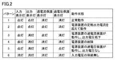
- FIG. 2 is a diagram showing a lighting pattern of the power supply device 100 according to the embodiment.
- "input indicator lamp”, “output indicator lamp”, “overcurrent protection indicator lamp”, and “overvoltage protection indicator lamp” mean an input display circuit 51, an output display circuit 52, and an overcurrent protection indicator, respectively. It indicates the circuit 53 and the indicator light (LED) of the overvoltage protection display circuit 55.
- Pattern 1 is a pattern in which the input indicator and output indicator are turned on and the overcurrent protection indicator and overvoltage protection indicator are turned off.
- Pattern 1 is a lighting pattern that represents a state in which the power supply device 100 operates normally.
- Pattern 2 is a pattern in which the input indicator, output indicator, and overcurrent protection indicator light turn on, and the overvoltage protection indicator light turns off.
- Pattern 2 is a lighting pattern that represents a state in which the power supply device 100 operates by exceeding the rated output current (that is, a predetermined output current range) of the power supply device 100.
- Pattern 3 is a pattern in which the input indicator lights, the output indicator lights go off, the overcurrent protection indicator light goes on, and the overvoltage protection indicator light goes off.
- Pattern 3 is a lighting pattern indicating a state in which the output voltage of the power supply device 100 has decreased as a result of the operation of the overcurrent protection.
- Pattern 4 is a pattern in which the input indicator lights up and the output indicators, overcurrent protection indicator lights, and overvoltage protection indicator lights go out. Pattern 4 is a lighting pattern indicating a state in which the power supply device 100 has failed.
- Pattern 5 is a pattern in which the input indicator lights up, the output indicator lights and overcurrent protection indicator lights go out, and the overvoltage protection indicator lights come on.
- Pattern 5 is a lighting pattern that represents a state in which the overvoltage protection of the power supply device 100 operates and the output voltage of the power supply device 100 is zero.
- Pattern 6 is a pattern in which all of the input indicator, output indicator, overcurrent protection indicator and overvoltage protection indicator are off. Pattern 6 is a state in which the input voltage is not supplied to the power supply device 100.
- the power supply device 100 is not provided with the overvoltage protection indicator light.
- the pattern 4 and the pattern 5 shown in FIG. 2 have the same lighting pattern. That is, when the output of the power supply device 100 is stopped, it is impossible to distinguish whether the cause is a malfunction of the power supply device 100 or an operation of overvoltage protection.
- the user has to analyze the state of the power supply device 100 in order to identify the cause.
- the user uses the measuring device to analyze the state of the power supply device 100.
- such analysis can be a burden on the user.
- the display by the overvoltage protection indicator light is combined with the display by the input indicator light, the output indicator light and the overcurrent protection indicator light. This allows the user to distinguish between pattern 4 and pattern 5.
- the overcurrent protection indicator light and the overvoltage protection indicator light are turned off.
- the overvoltage protection indicator light is turned off and the overvoltage protection indicator light is turned on.
- the output of the power supply device 100 is stopped, the user can visually identify only whether the cause is a malfunction of the power supply device 100 or an operation of overvoltage protection. This allows the user to easily identify the cause of the power supply device 100 stopping the output.
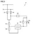
- FIG. 3 is a circuit diagram showing the configuration of the input display circuit according to the embodiment.
- the input display circuit 51 includes diodes D1 and D2, resistors R1, R2, R3 and R4, a shunt regulator 61, and a light emitting diode (LED) D3.
- LED light emitting diode
- the diode D1 and the diode D2 are connected to the power supply line (L) and the power supply line (N), respectively.
- the resistor R1 is connected to the diode D1 and the diode D2, and the resistor R2 is connected in series to the resistor R1.
- the resistor R3 is connected in parallel to the resistor R1 to the diode D1 and the diode D2, and the resistor R4 is connected to the resistor R3 in parallel to the light emitting diode D3.
- the light emitting diode D3 is an input indicator light.
- the shunt regulator 61 is connected to the connection point between the resistors R1 and R2, and is also connected to the resistors R2 and R4.
- the voltage input to the power supply line (L) and the power supply line (N) is divided by the resistors R1 and R2, and the divided voltage is input to the shunt regulator 61.
- the shunt regulator 61 compares the voltage with the shunt voltage. When a voltage equal to or higher than the shunt voltage is applied to the shunt regulator 61, the light emitting diode D3 lights up. Therefore, when the input voltage having the normal voltage value is supplied to the input unit 10, the light emitting diode D3 is turned on.
- the input voltage is an AC voltage (frequency is 50Hz or 60Hz)
- the input indicator light emitting diode D3
- the threshold value can be set by the shunt regulator 61, in one embodiment, the threshold value for turning on and off is set near the lower limit value of the operating voltage of the power supply device 100. This allows the user to determine whether or not the voltage required for the operation of the power supply device 100 is supplied.
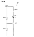
- FIG. 4 is a circuit diagram showing the configuration of the output display circuit according to the embodiment.
- the output display circuit 52 includes resistors R11, R12, R13, a light emitting diode D11, and a transistor Q11.
- the resistors R11 and R12 are connected in series.
- the resistor R13, the light emitting diode D11 and the transistor Q11 are connected in series.
- the light emitting diode D11 is an output indicator lamp.
- the base of the transistor Q11 is connected to the connection point between the resistors R11 and R12.
- the output voltage (Vout) of the power supply device 100 is divided according to the ratio of the resistance values of the resistors R11 and R12 to generate the base voltage of the transistor Q11.
- the transistor Q11 turns on and a current flows through the light emitting diode D11.
- the light emitting diode D11 is turned on.
- the output voltage Vout is normal, the light emitting diode D11 is turned on.
- the output voltage Vout decreases and the transistor Q11 turns off, the light emitting diode D11 turns off.
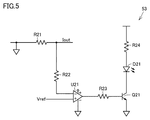
- FIG. 5 is a circuit diagram showing the configuration of the overcurrent protection display circuit according to the embodiment.
- “Overcurrent” refers to a state in which the output current (Iout) of the power supply device 100 exceeds 100% of the rating (expressed as Iout> 100%).
- the overcurrent protection display circuit 53 includes resistors R21, R22, R23, R24, a comparator U21, a light emitting diode D21, and a transistor Q21.
- the resistor R24, the light emitting diode D21, and the transistor Q21 are connected in series between a high voltage node (for example, a node of the voltage Vout) and the ground.
- the light emitting diode D21 is an overcurrent protection indicator lamp.
- the resistor R21 converts the output current Iout into a voltage.
- the comparator U21 compares the voltage with the reference voltage Vref. When the output current Iout exceeds a certain upper limit value, the output of the comparator U21 turns on the transistor Q21. As a result, a current flows through the light emitting diode D21 and the light emitting diode D21 lights up.
- the overcurrent protection display circuit 53 is a circuit for displaying to the user that the output current Iout is equal to or higher than the rated current. Therefore, the threshold value of the output current Iout (the value of the output current Iout when turning on the transistor Q21) is the current value when the load is 100%. That is, if Iout> 100%, the light emitting diode D21 is turned on.
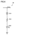
- FIG. 6 is a circuit diagram showing the configuration of the overvoltage detection circuit according to the embodiment.
- the overvoltage detection circuit 54 includes a Zener diode D31, a resistor R31, and a light emitting diode D32. Zener diode D31, resistor R31, and light emitting diode D32 are connected in series.
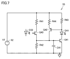
- FIG. 7 is a circuit diagram showing the configuration of the overcurrent protection display circuit according to the embodiment.
- the overvoltage protection display circuit 55 includes a voltage source 62, resistors R41, R42, R43, R44, transistors Q41, Q42, Q43, a capacitor C41, and a light emitting diode D41.
- the voltage source 62 corresponds to the rectifier circuit 21.
- the transistor Q43 constitutes a photocoupler together with the light emitting diode D32 shown in FIG.
- the light emitting diode D41 is an overvoltage protection indicator lamp.
- the overvoltage protection display circuit 55 includes a step-down circuit, and steps down the voltage V2 (voltage rectified by the rectifier circuit 21) from the voltage source 62.
- V2 voltage rectified by the rectifier circuit 21
- the output voltage Vout exceeds the Zener voltage of the Zener diode D31, a current flows through the light emitting diode D32 and the light emitting diode D32 lights up.
- the optical signal emitted by the light emitting diode D32 corresponds to the overvoltage detection signal.
- the transistor Q43 turns on in response to the overvoltage detection signal.
- the transistor Q43 When the transistor Q43 is turned on, the voltage V2 is divided by the resistors R41 and R42, and a voltage obtained by dividing the voltage V2 is supplied to the base of the transistor Q41.
- the light emitting diode D41 is turned on by turning on the transistor Q41.
- the overvoltage protection display circuit 55 is a self-holding circuit.
- a current flows through the light emitting diode D41, a voltage is applied to the base of the transistor Q42 by the resistor R43 and the transistor Q42 is turned on.
- a current flows through the transistor Q42 and a voltage is applied to the base of the transistor Q41 by the resistor R44. Therefore, the transistor Q41 can be kept in the ON state, and the light emitting diode D41 can be kept on.
- the overvoltage protection indicator light can be turned off by stopping the supply of the input voltage.
- FIG. 8 is a figure which shows typically an example of the external appearance of the power supply device 100 which concerns on embodiment of this invention.
- the input display circuit 51 and the output display circuit 52 are provided on the surface (front surface 102) of the housing 101 where the INPUT terminal, the DC-OUTPUT terminal, and the output voltage adjusting trimmer 84 are provided.
- the respective indicator lamps (LEDs) of the overcurrent protection display circuit 53 and the overvoltage protection display circuit 55 are arranged.
- the front surface is a surface facing the user when operating the power supply device 100.
- Output indicators, overcurrent protection indicators, and overvoltage protection indicators are centrally arranged on the front surface 102 of the housing 101.
- the input indicator lamp is arranged at a position apart from the output indicator lamp, the overcurrent protection indicator lamp, and the overvoltage protection indicator lamp.
- the user can easily understand that the abnormality has occurred in the power supply device 100. If the power supply device 100 is normal, the output indicator lights up. If the power supply device 100 is normal, the overcurrent protection indicator lamp and the overvoltage protection indicator lamp are off. Therefore, the output indicator light is off and the overcurrent protection indicator light or the overvoltage protection indicator light is on, so that the user can easily find the abnormality of the power supply device 100.
- the user should check whether the overvoltage protection indicator light is on. Thus, it is possible to determine whether the power supply device 100 is out of order or whether the overvoltage protection is activated (see FIG. 2).
- the power supply device 100 is arranged, for example, on a control panel at a manufacturing site.
- the user confirms the indicator lamp to determine whether the power supply device 100 is faulty or the protective function of the power supply device 100 is operating. Can be confirmed.
- the user can identify the cause of the voltage not being output from the power supply device 100 at an early stage, and therefore the time required for the subsequent maintenance can be shortened.
- overvoltage occurs instantaneously, so it is difficult to obtain reproducibility.
- the cause can be immediately identified by the user confirming whether or not the overvoltage protection indicator lamp is lit.
- the output current needs to be confirmed by a measuring device such as a clamp tester.
- a measuring device such as a clamp tester.
- the user or maintenance staff does not always have such a measuring device. Even in such a case, by checking the overcurrent protection indicator lamp, it is possible to easily grasp whether or not the output current is excessive.
- the power supply unit (20) activates overcurrent protection when the output current from the output unit (30) is an overcurrent exceeding a predetermined output current range, and outputs the output voltage from the output unit (30).
- the overvoltage protection is activated, An overcurrent protection indicator lamp (D21) that lights up during the operation of the overcurrent protection;
- the power supply device further comprising an overvoltage protection indicator lamp (D41) that lights up during the operation of the overvoltage protection.
- the power supply device has one surface (102) on which the input indicator light (D3), the output indicator light (D11), the overcurrent protection indicator light (D21) and the overvoltage protection indicator light (D41) are arranged.
- a housing (101) having The power supply device according to configuration 1, wherein the output indicator light (D11), the overcurrent protection indicator light (D21), and the overvoltage protection indicator light (D41) are intensively arranged on the one surface (102). ..
- the power supply unit (20) is A rectifying circuit (21) for rectifying the AC voltage when the input voltage is the AC voltage; A transformer (22) having a primary winding (22p) and a secondary winding (22s) connected to the output section (30); A switching circuit (23) for switching the voltage rectified by the rectification circuit (21) to generate a pulse voltage in the primary winding (22s) of the transformer (22),
- the power supply is An overvoltage detection circuit (54) for detecting the overvoltage in the output section (30) and generating an overvoltage detection signal; Upon receiving the overvoltage detection signal from the overvoltage detection circuit (54), the voltage rectified by the rectification circuit (21) is supplied to the overvoltage protection indicator lamp (D41) to turn on the overvoltage protection indicator lamp (D41).
- the power supply device according to configuration 1 or configuration 2, further comprising a lighting circuit (55) for lighting.
- 101 casing 102 front surface, C41 capacitor, D1, D2 diode, D3, D11, D21, D32, D41 light emitting diode, D31 Zener diode, Q11, Q21, Q41, Q42, Q43 transistor, R1 to R4, R11 to R13, R21 to R24, R31, R41 to R44 resistors, U21 comparator.
Landscapes
- Engineering & Computer Science (AREA)
- Power Engineering (AREA)
- Dc-Dc Converters (AREA)
- Power Conversion In General (AREA)
Abstract
電源装置の出力が停止した原因をユーザが容易に特定することが可能な電源装置を提供する。電源装置(100)は、入力表示灯(51)と、出力表示灯(52)と、過電流保護の動作時に点灯する過電流保護表示灯(53)と、電圧保護の動作時に点灯する過電圧保護表示灯(55)とを備える。電源装置(100)の故障時には過電流保護表示灯(53)と、過電圧保護表示灯(55)とが消灯する。一方、電源装置(100)の過電圧保護が動作するときには、過電流保護表示灯(53)が消灯し、過電圧保護表示灯(55)が点灯する。
Description
本発明は、電源装置に関する。
たとえば特開昭64-27579号公報(特許文献1)は、過電圧保護機能を有する電源回路を開示する。この電源回路は、過電圧検出回路および過電圧報知器を備えている。
一般に、電源装置が故障したときには電源装置の出力が停止する。しかし保護機能を有する電源装置の場合、その保護機能が動作することによって電源装置が出力を停止させる。したがって電源装置の出力が停止したときに、その原因をユーザが容易に特定できない可能性がある。
本発明の目的は、電源装置の出力が停止した原因をユーザが容易に特定することが可能な電源装置を提供することである。
本開示の一例によれば、電源装置は、外部からの入力電圧を受ける入力部と、入力部を通して入力された入力電圧から出力電圧を発生させる電源部と、出力電圧を出力する出力端子を含む出力部と、入力電圧が入力部に供給されることにより点灯する入力表示灯と、所定の出力範囲の出力電圧が出力部から出力されることにより点灯する出力表示灯とを備える。電源部は、出力部からの出力電流が所定の出力電流範囲を超える過電流である場合に過電流保護を動作させ、出力部からの出力電圧が所定の出力範囲を超える過電圧である場合に、過電圧保護を動作させる。電源装置は、過電流保護の動作時に点灯する過電流保護表示灯と、過電圧保護の動作時に点灯する過電圧保護表示灯とをさらに備える。
上記の構成によれば、電源装置の出力が停止した原因をユーザに容易に特定させることが可能な電源装置を提供することができる。電源装置の故障時には過電流保護表示灯と、過電圧保護表示灯とが消灯する。一方、電源装置の過電圧保護が動作するときには、過電流保護表示灯が消灯し、過電圧保護表示灯が点灯する。ユーザは、電源装置の出力が停止している場合に、その原因が電源装置の故障であるのか、過電圧保護の動作であるのかを目視のみで特定することができる。これにより、電源装置が出力を停止した原因をユーザが容易に特定することができる。
好ましくは、電源装置は、入力表示灯、出力表示灯、過電流保護表示灯および過電圧保護表示灯が配置された1つの面を有する筐体を備える。出力表示灯、過電流保護表示灯および過電圧保護表示灯は、1つの面において集中的に配置される。
上記の構成によれば、3つの表示灯の点灯状態を確認することにより、ユーザは電源装置に異常が発生したことを容易に把握することができる。
好ましくは、電源部は、入力電圧が交流電圧である場合に交流電圧を整流する整流回路と、一次巻線、および出力部に接続された二次巻線を有するトランスと、整流回路により整流された電圧をスイッチングして、トランスの一次巻線にパルス電圧を発生させる、スイッチング回路とを含む。電源装置は、出力部における過電圧を検出して、過電圧検出信号を発生させる過電圧検出回路と、過電圧検出回路からの過電圧検出信号を受けて、整流回路により整流された電圧を過電圧保護表示灯に供給して過電圧保護表示灯を点灯させる点灯回路とを備える。
上記によれば、過電圧保護が動作したときに過電圧保護表示灯を点灯させることができる。過電圧保護が動作すると電源装置の出力が停止する。しかし、表示灯を点灯させるためには、その表示灯への電力の供給が必要である。電源装置に入力電力が供給される間は整流回路から電力が出力されるので、過電圧保護が動作したときに過電圧保護表示灯を点灯させることができる。
好ましくは、点灯回路は、過電圧検出信号を受けることにより過電圧保護表示灯を点灯させ続ける自己保持回路である。
上記によれば、過電圧保護が動作したときに過電圧保護表示灯を点灯させることができる。一般に、過電圧の状態は、瞬間的に生じる。過電圧状態が解消したときに過電圧保護表示灯が消灯する場合、過電圧保護表示灯の点灯時間が非常に短くなる。ユーザが電源装置を常時監視するとは限らないので、ユーザは過電圧状態が発生したことを把握できない可能性が高い。点灯回路を自己保持回路とすることにより、過電圧状態が一旦発生すると、その後も過電圧保護表示灯が点灯し続けるので、ユーザにとって、過電圧状態が発生したことを把握しやすくすることができる。
本開示の一例によれば、電源装置の出力が停止した原因をユーザに容易に特定させることが可能な電源装置を提供することができる。
以下において、本実施の形態について図面を参照して詳しく説明する。なお、図中同一符号は同一または相当部分を示す。
<適用例>
まず、図1を用いて、本発明が適用される場面の一例について説明する。図1は、本実施の形態に係る電源装置100の一構成例を示したブロック図である。図1に示すように、電源装置100は、たとえばスイッチング電源装置である。電源装置100は、外部からの入力電圧を受ける入力部10と、電源部20と、出力部30とを含む。
まず、図1を用いて、本発明が適用される場面の一例について説明する。図1は、本実施の形態に係る電源装置100の一構成例を示したブロック図である。図1に示すように、電源装置100は、たとえばスイッチング電源装置である。電源装置100は、外部からの入力電圧を受ける入力部10と、電源部20と、出力部30とを含む。
たとえば入力部10は、図示しない交流電源(たとえば、50Hz/60Hz、100V/200Vの商用電源)に接続される。入力部10は、入力端子14,15(「AC(L)」)と、入力端子16,17(「AC(N)」)と、入力端子14~17に接続された保護回路であるフューズ11と、保護接地端子18とを含む。
電源部20は、入力部10を通して入力された電圧から出力電圧(電源電圧)を発生させる。一例として、電源部20は、整流回路21と、トランス22と、MOSFETを含むスイッチング回路23と、整流・平滑回路24とを含む。さらに、電源部20は、ノイズフィルタ25と、突入電流制限回路26と、高調波電流抑制回路27と、ドライブ制御回路28と、平滑回路29(一次側)と、電圧検出回路41と、過電圧検出回路42と、フォトカプラ43,44と、コンデンサ45,46と、電流検出回路47と、過電流検出回路48,49とを含む。
ノイズフィルタ25は、INPUTに入力された交流電圧に重畳した高周波のノイズ成分に対してフィルタリングを施し、ノイズ成分を除去した交流電圧を整流回路21に供給する。整流回路21は、フィルタリングされた交流電圧を整流する。
突入電流制限回路26は、例えば、抵抗と、この抵抗に並列に挿入されたリレーとから構成される。起動時から数十ミリ秒の間、リレーが開いて突入電流を防止する。その後に、リレーが閉じて電源装置100が起動される。高調波電流抑制回路27は、たとえばアクティブフィルタ方式の回路であり、高調波電流を低減する。平滑回路29は、平滑コンデンサで構成され、全波整流後の電圧を平滑化する。
トランス22は、一次巻線22p、二次巻線22sおよび補助巻線22aを備え、スイッチング回路23によって一次巻線22pに発生した高周波のパルス電圧を、二次巻線22sおよび補助巻線22aに誘導する。二次巻線22sは出力部30と電気的に接続されており、二次巻線22sに誘導された高周波のパルス電圧は、直流出力に利用される。補助巻線22aに誘導された高周波のパルス電圧は、ドライブ制御回路28の起動に利用される。
整流・平滑回路24は、整流回路および平滑コンデンサで構成され、トランス22の二次巻線22sに誘導された高周波のパルス電源(交流電源)を整流および平滑して、規定の出力電圧および出力電流を有する直流出力を発生させる。
電流検出回路47は、直流出力電源の出力電圧を、対応した降圧電圧で検出する。過電流検出回路48は、直流出力電源の出力電流が、規定の電流を超える場合に、過電流を検出する。
電圧検出回路41は、直流出力電源の出力電圧を、対応した降圧電圧で検出する。フォトカプラ43は、検出された降圧電圧に応じた信号、検出された電流に応じた信号、または、過電流の検出を示す信号をドライブ制御回路28に出力する。
過電圧検出回路42は、直流出力電源の出力電圧が、規定の電圧を超える場合に、過電圧を検出する。フォトカプラ44は、過電圧の検出を示す信号をドライブ制御回路28に出力する。
ドライブ制御回路28は、PWM(Pulse Width Modulation)信号発生器、フィードバック制御回路、OCP(Over Current Protect)端子、スイッチング駆動端子、駆動電源端子などを備えた制御ICにより構成される。ドライブ制御回路28は、PWM信号をスイッチング回路23に供給してスイッチング回路23を動作させる。
過電流の検出時には、ドライブ制御回路28は、フォトカプラ43からの信号に応答して、過電流保護動作を実行する。たとえばドライブ制御回路28は、スイッチング回路23が間欠発振を行うようにスイッチング回路23を制御する。一方、過電圧の検出時には、ドライブ制御回路28は、フォトカプラ44からの信号に応答して、過電圧保護動作を実行する。典型的には、ドライブ制御回路28は、スイッチング回路23のスイッチング動作を停止させる。したがって電源部20は、過電流保護および過電圧保護を動作するように構成されている。
電圧検出回路41で検出された二次側の電圧は、フォトカプラ43を介して、ドライブ制御回路28に帰還される。ドライブ制御回路28は、当該電圧に基づいてPWM信号のデューティ比を変更し、出力電圧である電源電圧が規定の電圧となるようにスイッチング回路23を駆動する。
スイッチング回路23は、トランス22の一次巻線22pと直列に接続される。スイッチング回路23は、ドライブ制御回路28から供給されたPWM信号に応答して一次側電圧をスイッチング(断続)して、トランス22の一次巻線22pに高周波のパルス電源を発生させる。
出力部30は、不足電圧検出出力回路31と、出力端子32,33(「+V」)と、出力端子34,35,36(「-V」)と、出力端子32,38(「DC LOW OUT」)とを含む。電源部20で発生した電源電圧は、出力端子32,33,34,35,36(「DC OUTPUT」とも表記する)から出力される。図1に示された構成では、電源電圧として直流電圧が出力される。
不足電圧検出出力回路31は、出力電圧の低下時に、電圧不足を示す信号を出力端子37,38を介して出力する。たとえば過電流保護の動作時に、電源装置100は間欠発振動作を行う。これにより電源装置100の出力電圧が低下するので、不足電圧検出出力回路31は、電圧不足を示す信号を出力する。
電源装置100は、さらに、入力表示回路51と、出力表示回路52と、過電流保護表示回路53と、過電圧検出回路54と、過電圧保護表示回路55とを含む。具体的には、入力表示回路51と、出力表示回路52と、過電流保護表示回路53と、過電圧保護表示回路55の各々は、点灯回路である。点灯回路は、表示灯であるLEDを含む。
入力表示回路51は、入力部10に接続される。入力電圧が入力部10に供給されるときに、入力表示回路51はLEDを点灯させる。
出力表示回路52は、出力部30に接続される。電源装置100が正常に動作するときに入力表示回路51はLEDを点灯させる。「正常に動作」とは、所定の出力電圧範囲内の出力電圧および所定の出力電流範囲内の出力電流が、出力部30から出力される状態である。
過電流保護表示回路53は、出力部30に接続され、電源装置100の過電流保護が動作したときにLEDを点灯させる。
過電圧検出回路54は、出力部30に接続され、電源装置100の出力電圧が過電圧であることを検出する。この場合、過電圧検出回路54は、過電圧検出信号を発生させる。
過電圧保護表示回路55は、電源装置100の過電圧保護が動作したときにLEDを点灯させる。
過電圧保護が動作すると、電源装置100は出力を停止する。このため、LEDを点灯させるための電力が必要となる。過電圧保護表示回路55は、整流回路21の出力電圧をLEDに供給することにより、LED(過電圧保護表示灯)を点灯させる。したがって、過電圧保護時に電源装置100が出力を停止していても過電圧保護表示回路55のLEDを点灯させることができる。
図2は、一実施形態に係る、電源装置100の点灯パターンを示した図である。図2において、「入力表示灯」、「出力表示灯」、「過電流保護表示灯」、および「過電圧保護表示灯」とは、それぞれ、入力表示回路51、出力表示回路52、過電流保護表示回路53、および過電圧保護表示回路55の表示灯(LED)を指す。
パターン1は、入力表示灯および出力表示灯が点灯し、過電流保護表示灯および過電圧保護表示灯が消灯するパターンである。パターン1は、電源装置100が正常に動作する状態を表す点灯パターンである。
パターン2は、入力表示灯、出力表示灯および過電流保護表示灯が点灯し、過電圧保護表示灯が消灯するパターンである。パターン2は、電源装置100が、電源装置100の定格出力電流(すなわち所定の出力電流範囲)を超えて動作する状態を表す点灯パターンである。
パターン3は、入力表示灯が点灯し、出力表示灯が消灯し、過電流保護表示灯が点灯し、過電圧保護表示灯が消灯するパターンである。パターン3は、過電流保護が動作した結果、電源装置100の出力電圧が低下した状態を表す点灯パターンである。
パターン4は、入力表示灯が点灯し、出力表示灯、過電流保護表示灯、および過電圧保護表示灯が消灯するパターンである。パターン4は、電源装置100が故障した状態を表す点灯パターンである。
パターン5は、入力表示灯が点灯し、出力表示灯および過電流保護表示灯が消灯し、過電圧保護表示灯が点灯するパターンである。パターン5は、電源装置100の過電圧保護が動作して、電源装置100の出力電圧が無しの状態を表す点灯パターンである。
パターン6は、入力表示灯、出力表示灯、過電流保護表示灯および過電圧保護表示灯のすべてが消灯するパターンである。パターン6は、電源装置100への入力電圧の供給が無い状態である。
ここで、過電圧保護表示灯が電源装置100に設けられていない例を考える。入力表示灯、出力表示灯および過電流保護表示灯のみによる点灯パターンの場合、図2に示したパターン4およびパターン5は、同一の点灯パターンになる。すなわち、電源装置100の出力が停止している場合に、その原因が、電源装置100の故障であるのか、過電圧保護の動作であるのかを区別することができない。
このような場合、ユーザは原因を特定するために電源装置100の状態を解析しなければならない。たとえば電源装置100の状態を解析するために、ユーザは測定装置を用いる。しかし、このような解析はユーザにとって負担となりえる。
この実施の形態では、過電圧保護表示灯による表示を、入力表示灯、出力表示灯および過電流保護表示灯の表示と組み合わせる。これにより、ユーザは、パターン4とパターン5とを区別することができる。電源装置100の故障時には過電流保護表示灯と、過電圧保護表示灯とが消灯する。一方、電源装置100の過電圧保護が動作するときには、過電流保護表示灯が消灯し、過電圧保護表示灯が点灯する。ユーザは、電源装置100の出力が停止している場合に、その原因が電源装置100の故障であるのか、過電圧保護の動作であるのかを目視のみで特定することができる。これにより、電源装置100が出力を停止した原因をユーザが容易に特定することができる。
<表示回路の構成>
以下に、本実施形態に係る表示回路の構成について説明する。しかしながら、以下に説明された構成は本発明を限定するものではない。
以下に、本実施形態に係る表示回路の構成について説明する。しかしながら、以下に説明された構成は本発明を限定するものではない。
図3は、一実施形態に係る入力表示回路の構成を示した回路図である。図3に示すように、入力表示回路51は、ダイオードD1,D2と、抵抗R1,R2,R3,R4と、シャントレギュレータ61と、発光ダイオード(LED)D3とを含む。
ダイオードD1およびダイオードD2は、それぞれ、電源ライン(L)および電源ライン(N)に接続される。抵抗R1は、ダイオードD1およびダイオードD2に接続され、抵抗R2が抵抗R1に直列に接続される。これにより入力電圧が分圧される。抵抗R3が抵抗R1と並列に、ダイオードD1およびダイオードD2に接続され、抵抗R4は、発光ダイオードD3と並列に抵抗R3に接続される。発光ダイオードD3は入力表示灯である。
シャントレギュレータ61は、抵抗R1と抵抗R2との接続点に接続されるとともに、抵抗R2および抵抗R4に接続される。電源ライン(L)および電源ライン(N)に、入力された電圧が抵抗R1および抵抗R2で分圧され、分圧された電圧が、シャントレギュレータ61に入力される。シャントレギュレータ61は、その電圧を、シャント電圧と比較する。シャント電圧以上の電圧がシャントレギュレータ61に印加されると、発光ダイオードD3が点灯する。したがって、正常な電圧値を有する入力電圧が入力部10に供給されると、発光ダイオードD3が点灯する。
入力電圧は交流電圧(周波数が50Hzまたは60Hz)であるため、入力表示灯(発光ダイオードD3)は交流電圧の周波数で点灯および消灯を繰り返す。しかしながらユーザの目視では実質的に確認できないほどの速さで点滅が繰り返されるので、視認性の問題は生じない。また、シャントレギュレータ61にて閾値設定をすることができるので、一実施形態では、電源装置100の動作電圧の下限値付近で、点灯および消灯の閾値が設定される。これにより電源装置100の動作に必要な電圧が供給されているか否かをユーザが判断できる。
図4は、一実施形態に係る出力表示回路の構成を示した回路図である。図4に示すように、出力表示回路52は、抵抗R11,R12,R13と、発光ダイオードD11と、トランジスタQ11とを含む。抵抗R11と抵抗R12とは直列に接続される。抵抗R13と、発光ダイオードD11とトランジスタQ11とは直列に接続される。発光ダイオードD11は出力表示灯である。
トランジスタQ11のベースは、抵抗R11と抵抗R12との接続点に接続される。電源装置100の出力電圧(Vout)が抵抗R11,R12の抵抗値の比に従って分割されることにより、トランジスタQ11のベース電圧が生成される。出力電圧Voutの値がある値に達すると、トランジスタQ11がオンして発光ダイオードD11に電流が流れる。これにより、発光ダイオードD11が点灯する。出力電圧Voutが正常であれば発光ダイオードD11が点灯する。一方、出力電圧Voutが低下してトランジスタQ11がオフすると発光ダイオードD11が消灯する。
図5は、一実施形態に係る過電流保護表示回路の構成を示した回路図である。「過電流」とは、電源装置100の出力電流(Iout)が、定格の100%を上回る状態を指す(Iout>100%と表記する)。図5に示すように、過電流保護表示回路53は、抵抗R21,R22,R23,R24と、比較器U21と、発光ダイオードD21と、トランジスタQ21とを含む。抵抗R24と、発光ダイオードD21とトランジスタQ21とは、高電圧ノード(たとえば電圧Voutのノード)と接地との間に直列に接続される。発光ダイオードD21は過電流保護表示灯である。
抵抗R21は、出力電流Ioutを電圧に変換する。比較器U21は、その電圧を基準電圧Vrefと比較する。出力電流Ioutがある上限値を上回る場合、比較器U21の出力によりトランジスタQ21がオンする。これにより、発光ダイオードD21に電流が流れて、発光ダイオードD21が点灯する。
この実施の形態では、過電流保護表示回路53は、出力電流Ioutが定格電流以上であることをユーザに表示する回路である。したがって、出力電流Ioutの閾値(トランジスタQ21をオンさせるときの出力電流Ioutの値)は負荷が100%であるときの電流値となる。すなわちIout>100%であれば発光ダイオードD21が点灯する。
図6は、一実施形態に係る過電圧検出回路の構成を示した回路図である。図6に示すように、過電圧検出回路54は、ツェナーダイオードD31と、抵抗R31と、発光ダイオードD32とを含む。ツェナーダイオードD31と、抵抗R31と、発光ダイオードD32とは直列に接続される。
図7は、一実施形態に係る過電流保護表示回路の構成を示した回路図である。図7に示すように、過電圧保護表示回路55は、電圧源62と、抵抗R41,R42,R43,R44と、トランジスタQ41,Q42,Q43と、キャパシタC41と、発光ダイオードD41とを含む。電圧源62は、整流回路21に相当する。トランジスタQ43は、図6に示した発光ダイオードD32とともにフォトカプラを構成する。発光ダイオードD41は、過電圧保護表示灯である。
過電圧保護表示回路55は、降圧回路を含み、電圧源62からの電圧V2(整流回路21により整流された電圧)を降圧する。出力電圧Voutが、ツェナーダイオードD31のツェナー電圧を上回ると発光ダイオードD32に電流が流れて発光ダイオードD32が点灯する。発光ダイオードD32が発する光信号は過電圧検出信号に対応する。トランジスタQ43は、過電圧検出信号に応答してオンする。
トランジスタQ43がオンすると、電圧V2が抵抗R41,R42により分圧され、トランジスタQ41のベースには、電圧V2を分圧した電圧が供給される。トランジスタQ41がオンすることにより発光ダイオードD41が点灯する。
過電圧保護表示回路55は、自己保持回路である。発光ダイオードD41に電流が流れると、抵抗R43によりトランジスタQ42のベースに電圧が与えられて、トランジスタQ42がオンする。これにより、トランジスタQ42に電流が流れるとともに、抵抗R44により、トランジスタQ41のベースに電圧が与えられる。したがって、トランジスタQ41は、オン状態を維持できるので、発光ダイオードD41を点灯させ続けることができる。
過電圧は一時的あるいは瞬間的にのみ発生することが多い。ユーザが電源装置100を常時監視するとは限らないので、過電圧状態の解消とともに表示灯が消灯する場合、ユーザが過電圧状態が発生したことを把握できない可能性が高い。過電圧保護表示回路55を自己保持回路とすることにより、過電圧状態が解消した後にも、過電圧保護表示回路55により発光ダイオードD41を点灯させ続けることができる。したがってユーザにとって、過電圧状態が発生したことを把握しやすくすることができる。なお、過電圧保護表示灯は、入力電圧の供給を停止することにより、消灯させることができる。
<表示灯の配置例>
図8は、本発明の実施形態に係る電源装置100の外観の一例を模式的に示す図である。図8に示すように、電源装置100では、筐体101のINPUTの端子、DC-OUTPUTの端子、出力電圧調整トリマ84を設けた面(前面102)に、入力表示回路51、出力表示回路52、過電流保護表示回路53、および過電圧保護表示回路55のそれぞれの表示灯(LED)が配置される。前面とは、電源装置100を操作する際にユーザと向きあう面である。
図8は、本発明の実施形態に係る電源装置100の外観の一例を模式的に示す図である。図8に示すように、電源装置100では、筐体101のINPUTの端子、DC-OUTPUTの端子、出力電圧調整トリマ84を設けた面(前面102)に、入力表示回路51、出力表示回路52、過電流保護表示回路53、および過電圧保護表示回路55のそれぞれの表示灯(LED)が配置される。前面とは、電源装置100を操作する際にユーザと向きあう面である。
出力表示灯、過電流保護表示灯、および過電圧保護表示灯は、筐体101の前面102に集中的に配置される。一方、入力表示灯は、出力表示灯、過電流保護表示灯、および過電圧保護表示灯から離れた位置に配置される。
電源装置100に異常が発生したときに、ユーザは、電源装置100に異常が発生したことを容易に把握することができる。電源装置100が正常であれば出力表示灯が点灯する。また、電源装置100が正常であれば、過電流保護表示灯および過電圧保護表示灯は消灯している。したがって、出力表示灯が消灯し、かつ、過電流保護表示灯または過電圧保護表示灯が点灯していることにより、ユーザが電源装置100の異常を容易に発見することができる。
特に、出力表示灯および過電流保護表示灯の両方が消灯している(かつ、入力表示灯が点灯している)場合、ユーザは、過電圧保護表示灯が点灯しているか否かを確認することにより、電源装置100が故障しているのか、過電圧保護が動作したのかを判断することができる(図2を参照)。
電源装置100は、たとえば製造現場の制御盤に配置される。仕様で定められた出力電圧が電源装置100から出力されない場合に、ユーザは表示灯を確認することにより電源装置100の故障であるか、電源装置100の保護機能が動作しているかのいずれであるかを確認できる。これによりユーザが早期に電源装置100から電圧が出力されない原因を特定できるので、事後保全にかかる時間を短縮することができる。
一般に、過電圧は瞬間的に発生するものであるため、再現性が得られにくい。また過電圧保護が動作したために電源装置100から電圧が出力されないという現象を、外部から確認することが難しい。この実施の形態では、過電圧保護表示灯が点灯しているか否かをユーザが確認することにより早急に原因を特定することができる。
また、通常では、出力電流は、クランプテスター等の測定装置により確認が必要である。しかしそのような測定装置をユーザあるいは保全担当者が常時持っているとは限らない。このような場合にも、過電流保護表示灯の確認により、出力電流が過大であるか否かを容易に把握することができる。
[付記]
以上のように、本実施形態は以下のような開示を含む。
以上のように、本実施形態は以下のような開示を含む。
(構成1)
外部からの入力電圧を受ける入力部(10)と、
前記入力部(10)を通して入力された前記入力電圧から出力電圧を発生させる電源部(20)と、
前記出力電圧を出力する出力端子を含む出力部(30)と、
前記入力電圧が前記入力部(10)に供給されることにより点灯する入力表示灯(D3)と、
所定の出力範囲の前記出力電圧が前記出力部(30)から出力されることにより点灯する出力表示灯(D11)とを備え、
前記電源部(20)は、前記出力部(30)からの出力電流が所定の出力電流範囲を超える過電流である場合に過電流保護を動作させ、前記出力部(30)からの前記出力電圧が前記所定の出力範囲を超える過電圧である場合に、過電圧保護を動作させ、
前記過電流保護の動作時に点灯する過電流保護表示灯(D21)と、
前記過電圧保護の動作時に点灯する過電圧保護表示灯(D41)とをさらに備える、電源装置。
外部からの入力電圧を受ける入力部(10)と、
前記入力部(10)を通して入力された前記入力電圧から出力電圧を発生させる電源部(20)と、
前記出力電圧を出力する出力端子を含む出力部(30)と、
前記入力電圧が前記入力部(10)に供給されることにより点灯する入力表示灯(D3)と、
所定の出力範囲の前記出力電圧が前記出力部(30)から出力されることにより点灯する出力表示灯(D11)とを備え、
前記電源部(20)は、前記出力部(30)からの出力電流が所定の出力電流範囲を超える過電流である場合に過電流保護を動作させ、前記出力部(30)からの前記出力電圧が前記所定の出力範囲を超える過電圧である場合に、過電圧保護を動作させ、
前記過電流保護の動作時に点灯する過電流保護表示灯(D21)と、
前記過電圧保護の動作時に点灯する過電圧保護表示灯(D41)とをさらに備える、電源装置。
(構成2)
前記電源装置は、前記入力表示灯(D3)、前記出力表示灯(D11)、前記過電流保護表示灯(D21)および前記過電圧保護表示灯(D41)が配置された1つの面(102)を有する筐体(101)を備え、
前記出力表示灯(D11)、前記過電流保護表示灯(D21)および前記過電圧保護表示灯(D41)は、前記1つの面(102)において集中的に配置される、構成1に記載の電源装置。
前記電源装置は、前記入力表示灯(D3)、前記出力表示灯(D11)、前記過電流保護表示灯(D21)および前記過電圧保護表示灯(D41)が配置された1つの面(102)を有する筐体(101)を備え、
前記出力表示灯(D11)、前記過電流保護表示灯(D21)および前記過電圧保護表示灯(D41)は、前記1つの面(102)において集中的に配置される、構成1に記載の電源装置。
(構成3)
前記電源部(20)は、
前記入力電圧が交流電圧である場合に前記交流電圧を整流する整流回路(21)と、
一次巻線(22p)および、前記出力部(30)に接続された二次巻線(22s)を有するトランス(22)と、
前記整流回路(21)により整流された電圧をスイッチングして、前記トランス(22)の前記一次巻線(22s)にパルス電圧を発生させる、スイッチング回路(23)とを含み、
前記電源装置は、
前記出力部(30)における前記過電圧を検出して、過電圧検出信号を発生させる過電圧検出回路(54)と、
前記過電圧検出回路(54)からの前記過電圧検出信号を受けて、前記整流回路(21)により整流された電圧を前記過電圧保護表示灯(D41)に供給して前記過電圧保護表示灯(D41)を点灯させる点灯回路(55)とを備える、構成1または構成2に記載の電源装置。
前記電源部(20)は、
前記入力電圧が交流電圧である場合に前記交流電圧を整流する整流回路(21)と、
一次巻線(22p)および、前記出力部(30)に接続された二次巻線(22s)を有するトランス(22)と、
前記整流回路(21)により整流された電圧をスイッチングして、前記トランス(22)の前記一次巻線(22s)にパルス電圧を発生させる、スイッチング回路(23)とを含み、
前記電源装置は、
前記出力部(30)における前記過電圧を検出して、過電圧検出信号を発生させる過電圧検出回路(54)と、
前記過電圧検出回路(54)からの前記過電圧検出信号を受けて、前記整流回路(21)により整流された電圧を前記過電圧保護表示灯(D41)に供給して前記過電圧保護表示灯(D41)を点灯させる点灯回路(55)とを備える、構成1または構成2に記載の電源装置。
(構成4)
前記点灯回路(55)は、前記過電圧検出信号を受けることにより前記過電圧保護表示灯(D41)を点灯させ続ける自己保持回路である、構成3に記載の電源装置。
前記点灯回路(55)は、前記過電圧検出信号を受けることにより前記過電圧保護表示灯(D41)を点灯させ続ける自己保持回路である、構成3に記載の電源装置。
本発明の実施の形態について説明したが、今回開示された実施の形態はすべての点で例示であって制限的なものではないと考えられるべきである。本発明の範囲は請求の範囲によって示され、請求の範囲と均等の意味および範囲内でのすべての変更が含まれることが意図される。
10 入力部、11 フューズ、14~17 入力端子、18 保護接地端子、20 電源部、21 整流回路、22 トランス、22a 補助巻線、22p 一次巻線、22s 二次巻線、23 スイッチング回路、24 整流・平滑回路、25 ノイズフィルタ、26 突入電流制限回路、27 高調波電流抑制回路、28 ドライブ制御回路、29 平滑回路、30 出力部、31 不足電圧検出出力回路31、32~38 出力端子、41 電圧検出回路、42,54 過電圧検出回路、43,44 フォトカプラ、45,46 コンデンサ、47 電流検出回路、48,49 過電流検出回路、51 入力表示回路、52 出力表示回路、53 過電流保護表示回路、55 過電圧保護表示回路、61 シャントレギュレータ、62 電圧源、84 出力電圧調整トリマ、100 電源装置。101 筐体、102 前面、C41 キャパシタ、D1,D2 ダイオード、D3,D11,D21,D32,D41 発光ダイオード、D31 ツェナーダイオード、Q11,Q21,Q41,Q42,Q43 トランジスタ、R1~R4,R11~R13,R21~R24,R31,R41~R44 抵抗、U21 比較器。
Claims (4)
- 電源装置であって、
外部からの入力電圧を受ける入力部と、
前記入力部を通して入力された前記入力電圧から出力電圧を発生させる電源部と、
前記出力電圧を出力する出力端子を含む出力部と、
前記入力電圧が前記入力部に供給されることにより点灯する入力表示灯と、
所定の出力範囲の前記出力電圧が前記出力部から出力されることにより点灯する出力表示灯とを備え、
前記電源部は、前記出力部からの出力電流が所定の出力電流範囲を超える過電流である場合に過電流保護を動作させ、前記出力部からの前記出力電圧が前記所定の出力範囲を超える過電圧である場合に、過電圧保護を動作させ、
前記過電流保護の動作時に点灯する過電流保護表示灯と、
前記過電圧保護の動作時に点灯する過電圧保護表示灯とをさらに備える、電源装置。 - 前記電源装置は、前記入力表示灯、前記出力表示灯、前記過電流保護表示灯および前記過電圧保護表示灯が配置された1つの面を有する筐体を備え、
前記出力表示灯、前記過電流保護表示灯および前記過電圧保護表示灯は、前記1つの面において集中的に配置される、請求項1に記載の電源装置。 - 前記電源部は、
前記入力電圧が交流電圧である場合に前記交流電圧を整流する整流回路と、
一次巻線および、前記出力部に接続された二次巻線を有するトランスと、
前記整流回路により整流された電圧をスイッチングして、前記トランスの前記一次巻線にパルス電圧を発生させる、スイッチング回路とを含み、
前記電源装置は、
前記出力部における前記過電圧を検出して、過電圧検出信号を発生させる過電圧検出回路と、
前記過電圧検出回路からの前記過電圧検出信号を受けて、前記整流回路により整流された電圧を前記過電圧保護表示灯に供給して前記過電圧保護表示灯を点灯させる点灯回路とを備える、請求項1または請求項2に記載の電源装置。 - 前記点灯回路は、前記過電圧検出信号を受けることにより前記過電圧保護表示灯を点灯させ続ける自己保持回路である、請求項3に記載の電源装置。
Applications Claiming Priority (2)
| Application Number | Priority Date | Filing Date | Title |
|---|---|---|---|
| JP2018-216143 | 2018-11-19 | ||
| JP2018216143A JP7014137B2 (ja) | 2018-11-19 | 2018-11-19 | 電源装置 |
Publications (1)
| Publication Number | Publication Date |
|---|---|
| WO2020105389A1 true WO2020105389A1 (ja) | 2020-05-28 |
Family
ID=70773302
Family Applications (1)
| Application Number | Title | Priority Date | Filing Date |
|---|---|---|---|
| PCT/JP2019/042804 Ceased WO2020105389A1 (ja) | 2018-11-19 | 2019-10-31 | 電源装置 |
Country Status (2)
| Country | Link |
|---|---|
| JP (1) | JP7014137B2 (ja) |
| WO (1) | WO2020105389A1 (ja) |
Citations (4)
| Publication number | Priority date | Publication date | Assignee | Title |
|---|---|---|---|---|
| JPS6364566A (ja) * | 1986-08-30 | 1988-03-23 | Fanuc Ltd | スイツチング電源保護回路 |
| JPH0468481U (ja) * | 1990-10-23 | 1992-06-17 | ||
| JP2005151674A (ja) * | 2003-11-14 | 2005-06-09 | Omron Corp | 電源装置 |
| JP2017158244A (ja) * | 2016-02-29 | 2017-09-07 | マスプロ電工株式会社 | 電源装置 |
-
2018
- 2018-11-19 JP JP2018216143A patent/JP7014137B2/ja active Active
-
2019
- 2019-10-31 WO PCT/JP2019/042804 patent/WO2020105389A1/ja not_active Ceased
Patent Citations (4)
| Publication number | Priority date | Publication date | Assignee | Title |
|---|---|---|---|---|
| JPS6364566A (ja) * | 1986-08-30 | 1988-03-23 | Fanuc Ltd | スイツチング電源保護回路 |
| JPH0468481U (ja) * | 1990-10-23 | 1992-06-17 | ||
| JP2005151674A (ja) * | 2003-11-14 | 2005-06-09 | Omron Corp | 電源装置 |
| JP2017158244A (ja) * | 2016-02-29 | 2017-09-07 | マスプロ電工株式会社 | 電源装置 |
Also Published As
| Publication number | Publication date |
|---|---|
| JP7014137B2 (ja) | 2022-02-01 |
| JP2020088942A (ja) | 2020-06-04 |
Similar Documents
| Publication | Publication Date | Title |
|---|---|---|
| JP6356688B2 (ja) | レトロフィット発光ダイオード管 | |
| US7791850B2 (en) | Ground fault circuit interrupter control circuit | |
| US20120235574A1 (en) | Fluorescent lamp drive and a protection circuit therein | |
| KR20140065377A (ko) | Led 램프, led 램프를 포함한 조명 장치, 및 led 램프의 전류 제어 방법 | |
| KR102291763B1 (ko) | 전원 장치 | |
| CN111181136A (zh) | 一种短路保护电路及供电系统 | |
| JP4748026B2 (ja) | 位相制御可能な直流定電流電源装置 | |
| JP5743436B2 (ja) | 照明装置、誘導灯及び非常灯 | |
| JP6186918B2 (ja) | Led点灯回路及びled照明装置 | |
| JP5877371B2 (ja) | 電源装置、点灯装置、灯具、及び車両 | |
| US11770886B2 (en) | LED driving circuit, light tube and illumination device | |
| US20120224400A1 (en) | Electrical equipment | |
| US11057974B2 (en) | Power supply device | |
| JP6687421B2 (ja) | 電源装置 | |
| JP7014137B2 (ja) | 電源装置 | |
| KR200195503Y1 (ko) | 고장 표시기능을 갖는 저전압 나트륨등용 안정기 회로 | |
| JP2008270048A (ja) | 放電灯点灯装置及び照明器具 | |
| JP6721215B2 (ja) | 点灯装置 | |
| KR910007046Y1 (ko) | 전원 단락시 ac입력 차단 회로 | |
| KR0155104B1 (ko) | 전원공급장치의 이상전압 보호회로 | |
| JP2024162654A (ja) | Led調光ユニット及びled点灯装置 | |
| US20190342972A1 (en) | Light source power supply | |
| KR20110133804A (ko) | 전자 접촉기의 표시 장치 | |
| JP2005026107A (ja) | 漏電検出表示回路 | |
| HK1196704B (en) | Led lamp, lighting device including led lamp, and method for controlling electric current of led lamp |
Legal Events
| Date | Code | Title | Description |
|---|---|---|---|
| 121 | Ep: the epo has been informed by wipo that ep was designated in this application |
Ref document number: 19887676 Country of ref document: EP Kind code of ref document: A1 |
|
| NENP | Non-entry into the national phase |
Ref country code: DE |
|
| 122 | Ep: pct application non-entry in european phase |
Ref document number: 19887676 Country of ref document: EP Kind code of ref document: A1 |