WO2020100477A1 - センサ装置 - Google Patents
センサ装置 Download PDFInfo
- Publication number
- WO2020100477A1 WO2020100477A1 PCT/JP2019/039855 JP2019039855W WO2020100477A1 WO 2020100477 A1 WO2020100477 A1 WO 2020100477A1 JP 2019039855 W JP2019039855 W JP 2019039855W WO 2020100477 A1 WO2020100477 A1 WO 2020100477A1
- Authority
- WO
- WIPO (PCT)
- Prior art keywords
- sensor element
- switch
- charge
- read
- sensor
- Prior art date
- Legal status (The legal status is an assumption and is not a legal conclusion. Google has not performed a legal analysis and makes no representation as to the accuracy of the status listed.)
- Ceased
Links
Images





Classifications
-
- H—ELECTRICITY
- H03—ELECTRONIC CIRCUITRY
- H03M—CODING; DECODING; CODE CONVERSION IN GENERAL
- H03M1/00—Analogue/digital conversion; Digital/analogue conversion
- H03M1/12—Analogue/digital converters
- H03M1/34—Analogue value compared with reference values
-
- H—ELECTRICITY
- H03—ELECTRONIC CIRCUITRY
- H03M—CODING; DECODING; CODE CONVERSION IN GENERAL
- H03M1/00—Analogue/digital conversion; Digital/analogue conversion
- H03M1/12—Analogue/digital converters
- H03M1/1205—Multiplexed conversion systems
- H03M1/121—Interleaved, i.e. using multiple converters or converter parts for one channel
-
- H—ELECTRICITY
- H04—ELECTRIC COMMUNICATION TECHNIQUE
- H04N—PICTORIAL COMMUNICATION, e.g. TELEVISION
- H04N25/00—Circuitry of solid-state image sensors [SSIS]; Control thereof
- H04N25/70—SSIS architectures; Circuits associated therewith
- H04N25/71—Charge-coupled device [CCD] sensors; Charge-transfer registers specially adapted for CCD sensors
- H04N25/75—Circuitry for providing, modifying or processing image signals from the pixel array
Definitions
- Embodiments of the present invention relate to a sensor drive circuit.
- a sensor drive circuit is connected to a sensor element including a photoelectric conversion element that generates an electric charge according to incident light, for example. Further, such a sensor drive circuit includes an A / D converter.
- the electric charge generated by the photoelectric conversion element is stored in the above-mentioned sensor element, and the sensor drive circuit can convert the electric charge (analog signal) into a digital signal by the A / D converter and output it.
- the digital signal output from the sensor drive circuit (A / D converter) in this way can be used for various processes.
- the resolution for the electric charge stored in the sensor element is limited to the bit width of the operational amplifier provided in the A / D converter, but it is desired to improve the resolution.
- the problem to be solved by the present invention is to provide a sensor drive circuit capable of improving the resolution with respect to the charges accumulated in the sensor element.
- the sensor drive circuit includes a switch, a control circuit, and an A / D converter.
- the switch is connected to a sensor element capable of storing electric charge, and is provided to read out the electric charge stored in the sensor element from the sensor element.
- the control circuit controls the switch so as to partially and sequentially read out charges accumulated in the sensor element.
- the A / D converter is connected to the switch, and outputs a digital signal obtained by A / D converting an analog signal corresponding to the charge, for each charge partially read through the switch.
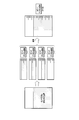
- FIG. 1 is a diagram showing a schematic configuration of a sensor module according to the first embodiment.
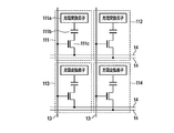
- FIG. 2 is a diagram showing an example of a circuit configuration of the sensor panel.
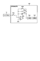
- FIG. 3 is a diagram illustrating an example of a configuration of a signal reading circuit included in the sensor driving circuit.
- FIG. 4 is a diagram for explaining an example of the operation of the sensor drive circuit in the comparative example of the present embodiment.
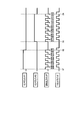
- FIG. 5 is a diagram for explaining an example of the operation of the sensor drive circuit according to the present embodiment.
- FIG. 6 is a diagram for explaining the A / D resolution in the comparative example of the present embodiment.
- FIG. 7 is a diagram for explaining the A / D resolution in this embodiment.
- FIG. 8 is a diagram conceptually showing a digital signal that can be obtained in the comparative example of the present embodiment.
- FIG. 9 is a diagram conceptually showing a digital signal that can be obtained in this embodiment.
- FIG. 10 is a diagram for explaining an example of the operation of the sensor drive circuit according to the second embodiment.
- FIG. 11 is a diagram showing an example of the configuration of a signal reading circuit including a resistor connected in parallel with a feedback capacitor and a reset switch.
- FIG. 12 is a diagram for explaining an example of the operation of the sensor drive circuit according to the third embodiment.
- FIG. 1 shows a schematic configuration of a sensor module (sensor device) according to this embodiment.
- the sensor module 10 shown in FIG. 1 includes a sensor panel 11 and a sensor drive circuit 12.
- each of the plurality of sensor elements arranged on the sensor panel 11 is configured to be able to store the charge generated by the photoelectric conversion element included in the sensor element.
- the sensor panel 11 (each of the plurality of sensor elements arranged on the sensor panel 11) is electrically connected to the sensor drive circuit 12 via a gate line 13 and a signal line 14.
- the sensor drive circuit 12 is a circuit for reading the electric charge stored in the above-mentioned sensor element from the sensor element and outputting an electric signal according to the read electric charge.
- the sensor drive circuit 12 includes a gate drive circuit 121, a signal read circuit 122, and a control circuit 123.
- the gate drive circuit 121 is connected to each of a plurality of sensor elements arranged on the sensor panel 11 via a gate line 13.
- the gate drive circuit 121 is a circuit for driving a sensor switch included in the sensor element in order to read the electric charge stored in the sensor element.
- the signal reading circuit 122 is a circuit for reading charges from each of a plurality of sensor elements arranged on the sensor panel 11 and outputting a digital signal obtained by A / D converting an analog signal corresponding to the charges.
- the control circuit 123 is a circuit for controlling the reading of charges from the sensor element by the signal reading circuit 122.
- the sensor panel 11 has a plurality of sensor elements arranged in a matrix. Note that, in FIG. 2, only four sensor elements 111 to 114 are shown for convenience.
- the configuration of the sensor element 111 among the four sensor elements 111 to 114 shown in FIG. 2 will be described below.
- the sensor element 111 includes a photoelectric conversion element 111a, a charge holding capacity (sensor pixel capacity) 111b, and a sensor switch 111c.
- the photoelectric conversion element 111a is an element that generates an electric charge according to the light with which the sensor panel 11 is irradiated as described above.
- a photodiode or the like is used as the photoelectric conversion element 111a, but the photoelectric conversion element 111a may be any other element as long as it generates an electric charge according to incident light.
- the photoelectric conversion element 111a does not have to be independent, and for example, a plurality of photoelectric conversion elements may be bundled into one sensor element.
- the charge storage capacitor 111b is a capacitor for storing the charge generated in the photoelectric conversion element 111a, and is electrically connected to the photoelectric conversion element 111a.
- the sensor switch 111c includes a thin film transistor (TFT: Thin Film Transistor).
- TFT Thin Film Transistor
- the sensor switch 111c includes, for example, a gate line 13 (sensor gate line) extending along a column in which a plurality of sensor elements are arranged, and a signal line 14 (sensor signal line) extending along a row in which the plurality of sensor elements are arranged. Are located near the intersection of.
- the gate electrode of the sensor switch 111c is electrically connected to the corresponding gate line 13.
- the source electrode of the sensor switch 111c is electrically connected to the corresponding signal line 14.
- the drain electrode of the sensor switch 111c is electrically connected to the charge storage capacitor 111b.
- the drain electrode of the sensor switch 111c may be connected to the signal line 13 and the source electrode of the sensor switch 111c may be connected to the charge storage capacitor 111b.
- the gate line 13 is connected to the gate drive circuit 121 included in the sensor drive circuit 12. Further, the signal line 14 is connected to the signal reading circuit 122 included in the sensor drive circuit 12.
- the gate drive circuit 121 sequentially applies the ON voltage to the gate line 13 and supplies the ON voltage to the gate electrode of the sensor switch 111c electrically connected to the gate line 13.
- the ON voltage is supplied to the gate electrode of the sensor switch 111c, the source electrode and the drain electrode of the sensor switch 111c are electrically connected.
- the charge stored in the charge storage capacitor 111b (that is, the charge generated in the photoelectric conversion element 111a) is output via the signal line 14, and the signal reading circuit 122 connected to the signal line 14 is The charge can be read.
- sensor element 111 has been described, but other sensor elements (sensor elements 112 to 114) have the same configuration.
- FIG. 3 shows an example of the configuration of the signal readout circuit 122 provided in the sensor drive circuit 12.
- the signal read circuit 122 includes a read switch 122a, an operational amplifier 122b, a feedback capacitor 122c, a reset switch 122d, a comparator 122e, and an integrator 122f.
- the read switch 122a is connected to each of the sensor elements arranged on the sensor panel 11, and is provided to read out the electric charge accumulated in the sensor element (charge holding capacitance) from the sensor element.
- the read switch 122a is in a state in which charges can be read from the sensor element (ON state) and a state in which the reading of charges from the sensor element is stopped (based on the control by the control circuit 123 included in the sensor drive circuit 12). Off state).
- the sensor element whose electric charge is read out by the signal readout circuit 122 via the readout switch 122a has an ON voltage applied to the gate electrode by the gate drive circuit 121 described above. It is a sensor element provided with a sensor switch being supplied. In other words, the sensor elements whose charges are read by the signal reading circuit 122 are sequentially selected by the gate driving circuit 121 that applies an on-voltage to the gate line.
- the operational amplifier 122b has a non-inverting input terminal (+), an inverting input terminal (-), and an output terminal.
- the reference voltage is input to the non-inverting input terminal, and the read switch 122a is electrically connected to the inverting input terminal.
- a feedback capacitor 122c is connected between the inverting input terminal and the output terminal of the operational amplifier 122b to form a negative feedback circuit.
- the operational amplifier 122b and the feedback capacitor 122c described above correspond to an integrator (integration circuit).
- the reset switch 122d is connected in parallel with the feedback capacitor 122c.
- the integrator described above can be reset by turning on the reset switch 122d.
- the comparator 122e is electrically connected to the output terminal of the operational amplifier 122b and compares the output signal of the operational amplifier 122b with the comparison signal.
- the operational amplifier 122b, the feedback capacitor 122c, the reset switch 122d and the comparator 122e described above constitute an A / D converter for A / D converting an analog signal and outputting a digital signal.
- a sensor drive circuit having a configuration in which the signal reading circuit 122 includes an operational amplifier 122b, a feedback capacitor 122c, a reset switch 122d, and a comparator 122e (that is, not including an integrator 122f) is used as a comparative example of the present embodiment.
- An example of the operation of the sensor drive circuit according to the comparative example will be described with reference to FIG.
- a sensor element including the sensor switch 1 (hereinafter referred to as a first sensor element) and a sensor element including a sensor switch 2 (hereinafter referred to as a second sensor element). Will be described).
- the gate drive circuit 121 supplies an on-voltage to the gate electrode of the sensor switch 1 to cause the source electrode-drain electrode of the sensor switch 1. There is continuity between the two.
- the read switch 122a is turned on.
- the electric charge stored in the first sensor element (charge holding capacitance provided in the first sensor element) can be input to the signal reading circuit 122 via the sensor switch 1 and the read switch 122a, and the electric charge can be read out. Be started.
- the time t12 is the time obtained by adding to the time t11 the time during which all the charges can be read from the first sensor element.
- the charge read from the first sensor element is converted into a digital signal by the A / D converter.
- the digital signal obtained by A / D converting the analog signal corresponding to the electric charge read from the first sensor element is output from the A / D converter.
- the reset switch 122d When the above A / D conversion is completed, the reset switch 122d is turned on to reset the integrator. When the reset of the integrator is completed, the reset switch 122d is turned off.
- the gate drive circuit 121 supplies an on-voltage to the gate electrode of the sensor switch 2 so that the source electrode and the drain electrode of the sensor switch 2 are electrically connected. To do.
- the read switch 122a is turned on.
- the charges stored in the second sensor element (charge holding capacitance provided in the second sensor element) can be input to the signal read circuit 122 via the sensor switch 2 and the read switch 122a, and the charge can be read. Be started.
- the time t14 is the time obtained by adding to the time t13 the time during which all the charges can be read from the second sensor element.
- the charge read from the second sensor element is converted into a digital signal by the A / D converter. According to this, a digital signal obtained by A / D converting an analog signal corresponding to the charges read from the second sensor element is output from the A / D converter.
- the reset switch 122d When the above A / D conversion is completed, the reset switch 122d is turned on to reset the integrator. When the reset of the integrator is completed, the reset switch 122d is turned off.
- the read charges are A / D converted by the A / D converter.
- the resolution for this charge (hereinafter referred to as A / D resolution) is limited to the bit width of the operational amplifier that constitutes the A / D converter.
- control circuit 123 has a configuration that controls the read switch 122a so as to partially and sequentially read out the charges accumulated in the sensor element.
- the A / D converter for each charge partially read by the control of the read switch 122a of the control circuit 123, is a digital signal obtained by A / D converting an analog signal corresponding to the charge. Is output.
- the signal read circuit 122 includes an integrator 122f electrically connected to an A / D converter (comparator) as shown in FIG.
- the integrator 122f integrates and outputs each digital signal output from the A / D converter for each partially read charge as described above.
- the gate drive circuit 121 supplies an on-voltage to the gate electrode of the sensor switch 1, so that the source electrode-drain electrode of the sensor switch 1 is supplied. There is continuity between the two.
- the read switch 122a is turned on.
- the electric charge stored in the first sensor element (charge holding capacitance provided in the first sensor element) can be input to the signal reading circuit 122 via the sensor switch 1 and the read switch 122a, and the electric charge can be read out. Be started.
- the read switch 122a when the reading of the charges accumulated in the first sensor element is started, the read switch 122a is maintained in the ON state until all the charges are read.
- the control circuit 123 temporarily turns off the read switch 122a when a part of the charge is read. Note that the control circuit 123 turns off the read switch 122a after the read switch 122a is turned on, for example, at a time interval shorter than the time at which all the charges stored in the first sensor element are read.
- a part of the electric charge stored in the first sensor element thus read (that is, the partially read electric charge) is converted into a digital signal by the A / D converter. According to this, a digital signal obtained by A / D converting an analog signal corresponding to the electric charges partially read from the first sensor element is output from the A / D converter.
- the reset switch 122d When the above A / D conversion is completed, the reset switch 122d is turned on to reset the integrator. When the reset of the integrator is completed, the reset switch 122d is turned off.
- control circuit 123 turns the read switch 122a on again, and turns the read switch 122a off again at the time interval described above. As a result, a part of the electric charge stored (remaining) in the first sensor element is read again.
- a series of operations including partial read-out of electric charges from the first sensor element, A / D conversion for the electric charges, and resetting of the integrator are accumulated in the first sensor element. Is repeated until the time when all can be read.
- a digital signal output from the A / D converter during the charge reading operation from the first sensor element (that is, an analog signal corresponding to the charge partially read from the first sensor element is
- Each of the D / D converted digital signals) is integrated by the integrator 122f.
- the result accumulated by the integrator 122f in this manner is output as the result of A / D conversion with respect to the charges accumulated in the first sensor element.
- the gate drive circuit 121 supplies an on-voltage to the gate electrode of the sensor switch 2 so that the source electrode and the drain electrode of the sensor switch 2 are electrically connected. To do.
- the read switch 122a is turned on.
- the charges stored in the second sensor element (charge holding capacitance provided in the second sensor element) can be input to the signal read circuit 122 via the sensor switch 2 and the read switch 122a, and the charge can be read. Be started.
- the operation after the charge reading from the second sensor element is started is similar to the above-described operation after the charge reading from the first sensor element is started. That is, a series of operations including partial charge reading from the second sensor element, A / D conversion for the charge, and resetting of the integrator can read all the charges stored in the second sensor element. Repeated until time has passed.
- a digital signal output from the A / D converter during the charge reading operation from the second sensor element (that is, an analog signal corresponding to the charge partially read from the second sensor element is referred to as A
- Each of the D / D converted digital signals) is integrated by the integrator 122f.
- the result accumulated by the integrator 122f in this manner is output as the result of the A / D conversion for the charges accumulated in the second sensor element.
- time interval from time t21 to time t24 shown in FIG. 5 may be the same as or different from the time interval from time t11 to t14 shown in FIG.
- the read switch 122a is controlled so that the charges accumulated in the sensor element are sequentially read out partially, and for each charge partially read through the read switch 122a, With the configuration of outputting a digital signal obtained by A / D converting an analog signal corresponding to the electric charge, it is possible to improve the resolution (A / D resolution) for the electric charge stored in the sensor element.
- FIG. 6 is a timing chart (gate clock) at which the ON voltage is supplied to the gate electrode of the sensor switch in the comparative example of the present embodiment, in which the analog signal corresponding to the electric charge read from the sensor element including the sensor switch is A /
- the relationship between the D conversion timing and the digital signal output as a result of the A / D conversion is shown.
- the number of times A / D conversion is performed on the charges read from the sensor element is 1, and the A / D resolution is provided in the A / D converter. Limited to the bit width of the operational amplifier. That is, in the comparative example of the present embodiment, it is possible to obtain a 3-bit digital signal that can represent the electric charge stored in the sensor element by 0 to 7.
- FIG. 7 is a timing at which an ON voltage is supplied to the gate electrode of the sensor switch according to the present embodiment (gate clock), and A / D conversion is performed on an analog signal corresponding to the charges read from the sensor element including the sensor switch. The relationship between the timing and the digital signal output as a result of the A / D conversion is shown.
- a / D conversion is performed for each charge partially read from the sensor element.
- the result of the A / D conversion for each partially read charge (3-bit digital signal) is integrated by the integrator 122f.
- the number of times A / D conversion is performed on the charges read from the sensor element is 4, and the respective results of the A / D conversion are integrated. According to this, as a result of the A / D conversion for the electric charge stored in the sensor element, a 5-bit digital signal capable of expressing the electric charge from 0 to 28 can be obtained.
- FIG. 8 is a diagram conceptually showing a digital signal (that is, A / D resolution in the comparative example of the present embodiment) that can be obtained in the comparative example of the present embodiment.
- FIG. 9 is a diagram conceptually showing a digital signal (that is, A / D resolution in this embodiment) that can be obtained in this embodiment.
- a 3-bit digital signal can be obtained for the charge stored in the sensor switch, whereas in the present embodiment as shown in FIG. A digital signal of substantially 5 bits can be obtained for the charge.
- the A / D resolution in the comparative example of the present embodiment is limited to the bit width of the operational amplifier
- the A / D resolution in the present embodiment is effectively “the bit width of the operational amplifier + log 2 (Number of A / D conversions) ”.
- the operational amplifier 122b has a bit width of 10 bits and the number of A / D conversions (the number of integrations) is 64.
- the sensor element has been described as having a photoelectric conversion element, but the present embodiment can be applied as long as the sensor element capable of storing an electric charge reads the electric charge. That is, the sensor element according to the present embodiment may be other than the sensor element including the photoelectric conversion element.
- the number of A / D conversions that is, the number of times of integration
- the number of times of integration performed in the operation of reading charges from the sensor element can be changed according to the charges (charge amount) stored in the sensor element. This point is different from the first embodiment described above.
- the gate drive circuit 121 supplies an on-voltage to the gate electrode of the sensor switch 1 to thereby cause the source electrode-drain electrode of the sensor switch 1 to flow. There is continuity between the two. Also, at time t31, the read switch 122a is turned on.
- the electric charge stored in the first sensor element (charge holding capacitance provided in the first sensor element) can be input to the signal reading circuit 122 via the sensor switch 1 and the read switch 122a, and the electric charge can be read out. Be started.
- control circuit 123 has a time longer than the time when all of the charges stored in the first sensor element are read after the read switch 122a is turned on, for example.
- the read switch 122a is turned off at short time intervals.
- a part of the electric charge stored in the first sensor element thus read (that is, the partially read electric charge) is converted into a digital signal by the A / D converter.
- the integrator is reset by turning on the reset switch 122d.
- the reset switch 122d is turned off.
- control circuit 123 in the present embodiment is a digital signal output from the A / D converter when the above A / D conversion is performed (that is, partially read from the first sensor element). Based on a digital signal obtained by A / D converting an analog signal corresponding to electric charge, it is determined whether to continue the operation of reading electric charge from the first sensor element.
- the control circuit 123 determines that the charge to be read remains in the first sensor element. , It is determined to continue the operation of reading the charge from the first sensor element. When the control circuit 123 determines that the read operation of the electric charge from the first sensor element is to be continued, the control circuit 123 turns the read switch 122a on again and the read operation is continued.
- the control circuit 123 determines that the first sensor element has no electric charge to be read and It is determined that the charge reading operation from one sensor element is not continued (that is, terminated). When it is determined by the control circuit 123 that the charge reading operation from the first sensor element is not continued, the charge reading operation from the first sensor element is completed, and the charge reading operation from the second sensor element is started. ..
- control circuit 123 notifies the gate drive circuit 121, for example, to the effect that the operation for reading the charge from the second sensor element is to be performed, so that between the source electrode and the drain electrode of the sensor switch 2 provided in the second sensor element. Control is performed so that the read switch 122a is turned on.
- a series of operations including partial charge reading from the first sensor element, A / D conversion for the charges, reset of the integrator, and determination of whether or not to continue the read operation are performed. It is repeated until it is determined that the read operation is not continued.
- the charge reading operation from the first sensor element is performed based on the digital signal obtained by A / D converting the analog signal corresponding to the charge read from the first sensor element when the time t32 is reached.
- the figure shows the case where it is determined that it will not continue.
- the charge reading operation from the second sensor element is started.
- the first sensor Since the operation is the same as the operation of reading charges from the element, detailed description thereof is omitted here.
- the time t33 and the time t34 shown in FIG. 10 in the charge reading operation from the second sensor element correspond to the time t31 and the time t32 in the charge reading operation from the first sensor element.
- the A / D conversion is performed 5 times in the charge reading operation from the first sensor element, whereas the A / D conversion is performed 5 times in the charge reading operation from the second sensor element.
- D conversion is performed 7 times.
- the number of A / D conversions (that is, the number of A / D conversions) is performed according to the charge (charge amount) stored in the first sensor element and the charge (charge amount) stored in the second sensor element. It is possible to change the cumulative number of times.
- the readout switch 122a is controlled based on the digital signal obtained by A / D converting the analog signal corresponding to the partially read charges.
- time from time t31 to time t32 shown in FIG. 10 is from time t21 to time t22 shown in FIG. 5 described in the above-described first embodiment. Less than time to.
- the number of A / D conversions (that is, the number of integrations) can be reduced, it can be expected to suppress the noise component that may be generated by the A / D conversion.
- the signal read circuit 122 in the present embodiment includes a resistor 122g connected in parallel with the feedback capacitor 122c and the reset switch 122d in order to prevent oscillation and remove low frequency components, as shown in FIG. 11, for example. May be.
- the read switch 122a is controlled based on the digital signal obtained by A / D converting the analog signal corresponding to the partially read charge (that is, the charge read operation from the sensor element is performed). However, the read switch 122a may be controlled based on the partially read charge (that is, the analog signal).
- the present embodiment differs from the above-described first embodiment in that the charge read time (that is, the integration interval) in the charge read operation from the sensor element is not constant.
- the electric charge stored in the sensor element is partially read out a plurality of times, so that the feedback capacitor 122c included in the signal reading circuit 122 is the same as that in the above-described first embodiment. It can be made smaller than that of the comparative example.
- the feedback capacitance 122c is configured to be small in this way, it is possible to realize downsizing and cost reduction of the sensor driving circuit 12 (signal reading circuit).
- the feedback capacitance 122c when the feedback capacitance 122c is made small, the feedback capacitance 122c (operational amplifier 122b) may be saturated by the electric charge read from the sensor element. Furthermore, at the start of the operation of reading out the charges from the sensor element, the efficiency of reading out the charges is higher than at the completion of the reading operation.
- the charge reading time (that is, the time for turning off the read switch 122a) is gradually increased.
- Adopt a configuration that does.
- the gate drive circuit 121 supplies an on-voltage to the gate electrode of the sensor switch 1, so that the source electrode-drain electrode of the sensor switch 1 is supplied. There is continuity between the two.
- the read switch 122a is turned on.
- the electric charge stored in the first sensor element (charge holding capacitance provided in the first sensor element) can be input to the signal reading circuit 122 via the sensor switch 1 and the read switch 122a, and the electric charge can be read out. Be started.
- control circuit 123 has a time longer than the time when all of the charges stored in the first sensor element are read after the read switch 122a is turned on, for example.
- the read switch 122a is turned off at short time intervals.
- a part of the electric charge stored in the first sensor element thus read (that is, the partially read electric charge) is converted into a digital signal by the A / D converter.
- the integrator is reset by turning on the reset switch 122d.
- the reset switch 122d is turned off.
- the control circuit 123 controls the time for reading out the charges from the first sensor element.
- the charge reading time from the first sensor element means a time period during which the read switch 122a is kept in the ON state for reading the charge from the first sensor element.
- the partial charge reading from the first sensor element, the A / D conversion for the charge, and the reset operation of the integrator are repeated four times. There is.
- control circuit 123 controls the read switch 122a so that the second read time is longer than the first read time, for example.
- the control circuit 123 controls the read switch 122a so that, for example, the read time of the third reading is longer than the read time of the second reading.
- the control circuit 123 controls the read switch 122a so that the read time of the fourth read is longer than the read time of the third read, for example.
- the second read time and the third read time are the same.
- the number of times charges are read from the first sensor element and each reading time are predetermined.
- the time from time t41 to time t42 shown in FIG. 12 (the time when the reading of the charges from the first sensor element is completed) is based on the number of times the charges are read from the first sensor element and each reading time. Can be determined.
- the charge reading operation from the second sensor element is started.
- the charge reading operation from the second sensor element is the first. Since the electric charge from the sensor element is similar to the read operation, detailed description thereof will be omitted here. Note that time t43 and time t44 shown in FIG. 10 in the charge reading operation from the second sensor element correspond to time t41 and time t42 in the charge reading operation from the first sensor element.
- the read switch 122a is controlled so as to read a part (first charge) of the electric charge accumulated in the sensor element, and the electric charge remains in the sensor element after being read.
- the read switch 122a is controlled so as to read a part (second charge) of the stored charge, and the time (second time) for reading the second charge is the time for reading the first charge (first time). ) It is over.
- the read switch 122a is controlled so that the charges are sampled in a short time at first and the charges are sampled in a longer time toward the latter half.
- the feedback capacitance 122c is made small as described above, the feedback capacitance 122c is prevented from being saturated, and the operation of reading the charge from the sensor element is performed efficiently. It becomes possible to do it.
- the number of A / D conversions (that is, the number of integrations) can be reduced, so that it is possible to suppress the noise component that may occur due to the A / D conversion.
- each read time in the operation of reading the charge from the sensor element has been described in advance, but the read time is the digital signal output from the A / D converter immediately before. It may be dynamically determined based on. Specifically, for example, the second read time shown in FIG. 12 may be determined based on a digital signal obtained by A / D converting an analog signal corresponding to the charges read in the first read time. The same applies to the third and subsequent read times.
- the configuration described in the second embodiment (that is, the charge from the sensor element based on the digital signal obtained by A / D converting the analog signal corresponding to the partially read charge) is used.
- a configuration for determining whether or not to continue the read operation) may be combined.
- a switch that is connected to a sensor element capable of storing electric charge and is provided to read out the electric charge stored in the sensor element from the sensor element, A control circuit for controlling the switch so as to partially and sequentially read out the charges accumulated in the sensor element;
- An A / D converter that is connected to the switch and outputs a digital signal obtained by A / D converting an analog signal corresponding to the charge for each charge partially read out through the switch;
- a sensor device comprising: [C2] The sensor device according to [C1], further including an integrator that integrates the digital signals output from the A / D converter for each of the partially read charges.
- the A / D converter is An operational amplifier having a first input terminal connected to the sensor element and a second input terminal to which a predetermined potential is applied; A feedback capacitor, a reset switch and a resistor connected in parallel between the first input terminal and the output terminal of the operational amplifier; A comparator connected to the output terminal of the operational amplifier; including The sensor device according to [C4].
- the control circuit controls the switch so as to read a first electric charge, which is a part of the electric charge stored in the sensor element, and the electric charge remaining in the sensor element after the first electric charge is read out.
- a / D conversion method executed by a sensor device, which is connected to a sensor element capable of storing electric charge and includes a switch for reading the electric charge stored in the sensor element from the sensor element, Controlling the switch to partially sequentially read out the charge stored in the sensor element; Outputting a digital signal obtained by A / D converting an analog signal corresponding to the charge, for each charge partially read through the switch.
- a / D conversion method comprising: [C10] The A / D conversion method according to [C9], further comprising the step of integrating digital signals output for each of the partially read charges. [C11] The A / D conversion method according to [C9], wherein the controlling includes controlling the switch based on the output digital signal.
- the controlling is Controlling the switch to read more charge from the sensor element if the value of the output digital signal is not less than or equal to a predetermined value; Controlling the switch so as to start reading charges from a sensor element different from the sensor element when the value of the output digital signal is less than or equal to the predetermined value.
- the outputting is performed by an A / D converter
- the A / D converter is An operational amplifier having a first input terminal connected to the sensor element and a second input terminal to which a predetermined potential is applied; A feedback capacitor, a reset switch and a resistor connected in parallel between the first input terminal and the output terminal of the operational amplifier; A comparator connected to the output terminal of the operational amplifier The A / D conversion method described in [C12].
- the controlling controls the switch so as to read a first electric charge, which is a part of the electric charge stored in the sensor element, and remains in the sensor element after the first electric charge is read out.
- the second time during which the second charge is read out by controlling the switch is equal to or longer than the first time during which the first charge is read out by controlling the switch.
Landscapes
- Engineering & Computer Science (AREA)
- Theoretical Computer Science (AREA)
- Multimedia (AREA)
- Signal Processing (AREA)
- Transforming Light Signals Into Electric Signals (AREA)
- Facsimile Heads (AREA)
Abstract
実施形態に係るセンサ装置は、スイッチと、制御回路と、A/D変換器とを具備する。スイッチは、電荷を蓄えることが可能なセンサ素子に接続され、センサ素子に蓄えられた電荷を当該センサ素子から読み出すために設けられる。制御回路は、センサ素子に蓄えられた電荷を部分的に順次読み出すようにスイッチを制御する。A/D変換器は、スイッチに接続され、当該スイッチを介して部分的に読み出された電荷毎に、当該電荷に応じたアナログ信号をA/D変換したデジタル信号を出力する。
Description
本発明の実施形態は、センサ駆動回路に関する。
一般に、例えば入射光に応じた電荷を発生する光電変換素子を含むセンサ素子にはセンサ駆動回路が接続されている。また、このようなセンサ駆動回路は、A/D変換器を備える。
上記したセンサ素子には光電変換素子で発生した電荷が蓄えられており、センサ駆動回路は、A/D変換器により、当該電荷(アナログ信号)をデジタル信号に変換して出力することができる。このようにセンサ駆動回路(A/D変換器)から出力されたデジタル信号は、各種処理に用いることができる。
ここで、上記したセンサ素子に蓄えられている電荷に対する分解能はA/D変換器に備えられる演算増幅器のビット幅に制限されるが、当該分解能を向上させることが望まれている。
そこで、本発明が解決しようとする課題は、センサ素子に蓄えられている電荷に対する分解能を向上させることが可能なセンサ駆動回路を提供することにある。
実施形態に係るセンサ駆動回路は、スイッチと、制御回路と、A/D変換器とを具備する。前記スイッチは、電荷を蓄えることが可能なセンサ素子に接続され、前記センサ素子に蓄えられた電荷を当該センサ素子から読み出すために設けられる。前記制御回路は、前記センサ素子に蓄えられた電荷を部分的に順次読み出すように前記スイッチを制御する。前記A/D変換器は、前記スイッチに接続され、当該スイッチを介して部分的に読み出された電荷毎に、当該電荷に応じたアナログ信号をA/D変換したデジタル信号を出力する。
以下、図面を参照して、各実施形態について説明する。
なお、開示はあくまで一例に過ぎず、当業者において、発明の趣旨を保っての定義変更について容易に想到するものについては、当然に本発明の範囲に含有される。また、図面は、説明をより明確にするため、実際の態様に比べて模式的に表される場合があるが、あくまで一例であって、本発明の解釈を限定するものではない。各図において、連続して配置される同一または類似の要素については符号を省略することがある。また、本明細書と各図において、既出の図に関して前述したものと同一または類似した機能を発揮する構成要素には同一の参照符号を付し、重複する詳細な説明を省略することがある。
なお、開示はあくまで一例に過ぎず、当業者において、発明の趣旨を保っての定義変更について容易に想到するものについては、当然に本発明の範囲に含有される。また、図面は、説明をより明確にするため、実際の態様に比べて模式的に表される場合があるが、あくまで一例であって、本発明の解釈を限定するものではない。各図において、連続して配置される同一または類似の要素については符号を省略することがある。また、本明細書と各図において、既出の図に関して前述したものと同一または類似した機能を発揮する構成要素には同一の参照符号を付し、重複する詳細な説明を省略することがある。
(第1実施形態)
まず、第1実施形態について説明する。図1は、本実施形態に係るセンサモジュール(センサ装置)の概略構成を示す。
まず、第1実施形態について説明する。図1は、本実施形態に係るセンサモジュール(センサ装置)の概略構成を示す。
図1に示すセンサモジュール10は、センサパネル11及びセンサ駆動回路12を備える。
センサパネル11には、例えば画面(パネル)に照射された光(入射光)に応じた電荷を発生する光電変換素子を有する複数のセンサ素子が例えばマトリクス状に配置されている。なお、センサパネル11に配置されている複数のセンサ素子の各々は、当該センサ素子が有する光電変換素子で発生した電荷を蓄えることが可能なように構成されている。
センサパネル11(当該センサパネル11に配置されている複数のセンサ素子の各々)は、ゲート線13及び信号線14を介してセンサ駆動回路12と電気的に接続されている。
センサ駆動回路12は、上記したセンサ素子に蓄えられた電荷を当該センサ素子から読み出して、当該読み出された電荷に応じた電気信号を出力するための回路である。センサ駆動回路12は、ゲート駆動回路121、信号読み出し回路122及び制御回路123を備える。
ゲート駆動回路121は、センサパネル11に配置されている複数のセンサ素子の各々とゲート線13を介して接続される。ゲート駆動回路121は、当該センサ素子に蓄えられた電荷を読み出すために当該センサ素子に備えられるセンサスイッチを駆動するための回路である。
信号読み出し回路122は、センサパネル11に配置されている複数のセンサ素子の各々から電荷を読み出し、当該電荷に応じたアナログ信号をA/D変換したデジタル信号を出力するための回路である。
制御回路123は、信号読み出し回路122によるセンサ素子からの電荷の読み出しを制御するための回路である。
図2は、図1に示すセンサパネル11の回路構成の一例を示す。センサパネル11には、上記したように複数のセンサ素子がマトリクス状に配置されている。なお、図2においては、便宜的に、4つのセンサ素子111~114のみが示されている。
以下、図2に示す4つのセンサ素子111~114のうちのセンサ素子111の構成について説明する。
センサ素子111は、光電変換素子111a、電荷保持容量(センサ画素容量)111b及びセンサスイッチ111cを備える。
光電変換素子111aは、上記したようにセンサパネル11に照射された光に応じた電荷を発生する素子である。光電変換素子111aとしては例えばフォトダイオード等が用いられるが、当該光電変換素子111aは、入射光に応じて電荷を発生するものであれば他のものであってもよい。また、光電変換素子111aは単独である必要はなく、例えば複数の光電変換素子を束ねてひとつのセンサ素子としてもよい。
電荷保持容量111bは、光電変換素子111aで発生した電荷を蓄えるためのキャパシタ(コンデンサ)であり、当該光電変換素子111aと電気的に接続されている。
センサスイッチ111cは、薄膜トランジスタ(TFT:Thin Film Transistor)を含む。センサスイッチ111cは、例えば、複数のセンサ素子が配列する列に沿って延びるゲート線13(センサゲート線)と当該複数のセンサ素子が配列する行に沿って延びる信号線14(センサ信号線)とが交差する位置近傍に配置されている。
センサスイッチ111cのゲート電極は、対応するゲート線13と電気的に接続されている。センサスイッチ111cのソース電極は、対応する信号線14と電気的に接続されている。センサスイッチ111cのドレイン電極は、電荷保持容量111bと電気的に接続されている。なお、センサスイッチ111cのドレイン電極が信号線と13と接続され、当該センサスイッチ111cのソース電極が電荷保持容量111bと接続される構成であってもよい。
ここで、上記したようにゲート線13は、センサ駆動回路12に備えられるゲート駆動回路121と接続されている。また、信号線14は、センサ駆動回路12に備えられる信号読み出し回路122と接続されている。
ゲート駆動回路121は、ゲート線13にオン電圧を順次印加して、当該ゲート線13に電気的に接続されたセンサスイッチ111cのゲート電極にオン電圧を供給する。センサスイッチ111cのゲート電極にオン電圧が供給された場合、当該センサスイッチ111cのソース電極-ドレイン電極間が導通する。
これにより、電荷保持容量111bに蓄えられている電荷(つまり、光電変換素子111aで発生した電荷)が信号線14を介して出力され、当該信号線14と接続されている信号読み出し回路122は、当該電荷を読み出すことができる。
ここでは、センサ素子111の構成についてのみ説明したが、他のセンサ素子(センサ素子112~114)についても同様の構成を有する。
図3は、センサ駆動回路12に備えられる信号読み出し回路122の構成の一例を示す。信号読み出し回路122は、読み出しスイッチ122a、演算増幅器122b、帰還容量122c、リセットスイッチ122d、比較器122e及び積算器122fを備える。
読み出しスイッチ122aは、センサパネル11に配置されているセンサ素子の各々に接続され、当該センサ素子(電荷保持容量)に蓄えられた電荷を当該センサ素子から読み出すために設けられている。
読み出しスイッチ122aは、センサ駆動回路12に備えられる制御回路123による制御に基づいて、センサ素子から電荷を読み出すことが可能な状態(オン状態)及び当該センサ素子からの電荷の読み出しを停止した状態(オフ状態)を切り替える。
なお、センサパネル11には複数のセンサ素子が配置されているが、読み出しスイッチ122aを介して信号読み出し回路122によって電荷が読み出されるセンサ素子は、上記したゲート駆動回路121によってゲート電極にオン電圧が供給されているセンサスイッチを備えるセンサ素子である。換言すれば、信号読み出し回路122によって電荷が読み出されるセンサ素子は、ゲート線にオン電圧を印加するゲート駆動回路121によって順次選択される。
演算増幅器122bは、非反転入力端子(+)、反転入力端子(-)及び出力端子を有する。非反転入力端子には基準電圧が入力され、反転入力端子には読み出しスイッチ122aが電気的に接続されている。
また、演算増幅器122bの反転入力端子及び出力端子間には帰還容量122cが接続され、負帰還回路が構成されている。なお、上記した演算増幅器122b及び帰還容量122cは、積分器(積分回路)に相当する。
リセットスイッチ122dは、帰還容量122cに並列に接続されている。信号読み出し回路122においては、リセットスイッチ122dをオン状態とすることによって、上記した積分器をリセットすることができる。
比較器122eは、演算増幅器122bの出力端子と電気的に接続されており、当該演算増幅器122bの出力信号と比較信号とを比較する。
本実施形態において、上記した演算増幅器122b、帰還容量122c、リセットスイッチ122d及び比較器122eは、アナログ信号をA/D変換してデジタル信号を出力するためのA/D変換器を構成する。
ここで、信号読み出し回路122が演算増幅器122b、帰還容量122c、リセットスイッチ122d及び比較器122eを備える(つまり、積算器122fを備えない)構成のセンサ駆動回路を本実施形態の比較例とし、図4を参照して、当該比較例に係るセンサ駆動回路の動作の一例について説明する。
ここでは、センサパネル11に配置されている複数のセンサ素子のうち、センサスイッチ1を備えるセンサ素子(以下、第1センサ素子と表記)及びセンサスイッチ2を備えるセンサ素子(以下、第2センサ素子と表記)から順次電荷を読み出す場合の動作について説明する。
まず、第1センサ素子から電荷を読み出す場合、図4に示す時刻t11において、ゲート駆動回路121からセンサスイッチ1のゲート電極にオン電圧が供給されることによって、センサスイッチ1のソース電極-ドレイン電極間が導通する。また、時刻t11においては、読み出しスイッチ122aをオン状態とする。
これにより、第1センサ素子(第1センサ素子に備えられる電荷保持容量)に蓄えられている電荷がセンサスイッチ1及び読み出しスイッチ122aを介して信号読み出し回路122に入力可能となり、当該電荷の読み出しが開始される。
ここで、時刻t12に到達した場合、第1センサ素子からの電荷の読み出しを終了する。この場合、センサスイッチ1のゲート電極に対するオン電圧の供給を停止するとともに、読み出しスイッチ122aをオフ状態とする(つまり、第1センサ素子からの電荷の読み出しを停止する)。時刻t12は、時刻t11に対して、第1センサ素子から全ての電荷を読み出すことが可能な時間が加算された時刻であるものとする。
なお、第1センサ素子から読み出された電荷は、A/D変換器によってデジタル信号に変換される。これによれば、第1センサ素子から読み出された電荷に応じたアナログ信号をA/D変換したデジタル信号がA/D変換器から出力される。
上記したA/D変換が完了した場合、リセットスイッチ122dをオン状態とすることによって積分器がリセットされる。積分器のリセットが完了すると、リセットスイッチ122dをオフ状態とする。
次に、第2センサ素子から電荷を読み出す場合、時刻t13において、ゲート駆動回路121からセンサスイッチ2のゲート電極にオン電圧が供給されることによって、センサスイッチ2のソース電極-ドレイン電極間が導通する。また、時刻t13においては、読み出しスイッチ122aをオン状態とする。
これにより、第2センサ素子(第2センサ素子に備えられる電荷保持容量)に蓄えられている電荷がセンサスイッチ2及び読み出しスイッチ122aを介して信号読み出し回路122に入力可能となり、当該電荷の読み出しが開始される。
ここで、時刻t14に到達した場合、第2センサ素子からの電荷の読み出しを終了する。この場合、センサスイッチ2のゲート電極に対するオン電圧の供給を停止するとともに、読み出しスイッチ122aをオフ状態とする(つまり、第2センサ素子からの電荷の読み出しを停止する)。時刻t14は、時刻t13に対して、第2センサ素子から全ての電荷を読み出すことが可能な時間が加算された時刻であるものとする。
なお、第2センサ素子から読み出された電荷は、A/D変換器によってデジタル信号に変換される。これによれば、第2センサ素子から読み出された電荷に応じたアナログ信号をA/D変換したデジタル信号がA/D変換器から出力される。
上記したA/D変換が完了した場合、リセットスイッチ122dをオン状態とすることによって積分器がリセットされる。積分器のリセットが完了すると、リセットスイッチ122dをオフ状態とする。
ここでは第1センサ素子及び第2センサ素子から電荷を読み出す場合について説明したが、他のセンサ素子からも同様に電荷が読み出される。
ここで、本実施形態の比較例においては、例えば第1センサ素子に蓄えられている電荷を全て読み出し、A/D変換器によって当該読み出された電荷(アナログ信号)がA/D変換されるが、この電荷に対する分解能(以下、A/D分解能と表記)は、当該A/D変換器を構成する演算増幅器のビット幅に制限される。
しかしながら、センサ素子に蓄えられている電荷に対して精度の高いデジタル信号を出力するためには、上記したA/D分解能を向上させる必要がある。
そこで、本実施形態においては、制御回路123がセンサ素子に蓄えられている電荷を部分的に順次読み出すように読み出しスイッチ122aを制御する構成を有する。
このような構成の場合、A/D変換器は、制御回路123の読み出しスイッチ122aに対する制御によって部分的に読み出された電荷毎に、当該電荷に応じたアナログ信号をA/D変換したデジタル信号を出力する。
ここで、本実施形態において、信号読み出し回路122は、図3に示すようにA/D変換器(比較器)と電気的に接続された積算器122fを備える。
積算器122fは、上記したように部分的に読み出された電荷毎にA/D変換器から出力されるデジタル信号の各々を積算して出力する。
以下、図5を参照して、本実施形態におけるセンサ駆動回路の動作(センサ素子からの電荷の読み出し動作)の一例について説明する。ここでは、上記した図4と同様に、センサパネル11に配置されている複数のセンサ素子のうち、センサスイッチ1を備える第1センサ素子及びセンサスイッチ2を備える第2センサ素子から順次電荷を読み出す場合の動作について説明する。
まず、第1センサ素子から電荷を読み出す場合、図5に示す時刻t21において、ゲート駆動回路121からセンサスイッチ1のゲート電極にオン電圧が供給されることによって、センサスイッチ1のソース電極-ドレイン電極間が導通する。また、時刻t21においては、読み出しスイッチ122aをオン状態とする。
これにより、第1センサ素子(第1センサ素子に備えられる電荷保持容量)に蓄えられている電荷がセンサスイッチ1及び読み出しスイッチ122aを介して信号読み出し回路122に入力可能となり、当該電荷の読み出しが開始される。
ここで、上記した本実施形態の比較例においては、第1センサ素子に蓄えられている電荷の読み出しが開始された場合、当該電荷を全て読み出すまで読み出しスイッチ122aのオン状態が維持されるが、本実施形態において、制御回路123は、当該電荷の一部が読み出された時点で読み出しスイッチ122aを一旦オフ状態とする。なお、制御回路123は、読み出しスイッチ122aがオン状態にされた後、例えば第1センサ素子に蓄えられている電荷の全てが読み出される時間よりも短い時間間隔で読み出しスイッチ122aをオフ状態とする。
このように読み出された第1センサ素子に蓄えられている電荷の一部(つまり、部分的に読み出された電荷)は、A/D変換器によってデジタル信号に変換される。これによれば、第1センサ素子から部分的に読み出された電荷に応じたアナログ信号をA/D変換したデジタル信号がA/D変換器から出力される。
上記したA/D変換が完了した場合、リセットスイッチ122dをオン状態とすることによって積分器がリセットされる。積分器のリセットが完了すると、リセットスイッチ122dをオフ状態とする。
次に、制御回路123は、読み出しスイッチ122aを再度オン状態とし、上記した時間間隔で当該読み出しスイッチ122aを再度オフ状態とする。これにより、第1センサ素子に蓄えられている(残存している)電荷の一部が再度読み出される。
本実施形態においては、このような第1センサ素子からの部分的な電荷の読み出し、当該電荷に対するA/D変換及び積分器のリセットを含む一連の動作が第1センサ素子に蓄えられている電荷を全て読み出すことが可能な時間が経過するまで繰り返される。
具体的には、図5に示す例では、時刻t22に到達した際に第1センサ素子からの読み出しを終了し、当該第1センサ素子から最後に読み出された電荷をA/D変換し、積分器をリセットする。これにより、第1センサ素子からの電荷の読み出し動作が完了する。
なお、この第1センサ素子からの電荷の読み出し動作の間にA/D変換器から出力されたデジタル信号(つまり、第1センサ素子から部分的に読み出された電荷に応じたアナログ信号をA/D変換したデジタル信号の各々)は、積算器122fによって積算される。本実施形態においては、このように積算器122fによって積算された結果が第1センサ素子に蓄えられている電荷に対するA/D変換の結果として出力される。
次に、第2センサ素子から電荷を読み出す場合、時刻t23において、ゲート駆動回路121からセンサスイッチ2のゲート電極にオン電圧が供給されることによって、センサスイッチ2のソース電極-ドレイン電極間が導通する。また、時刻t23においては、読み出しスイッチ122aをオン状態とする。
これにより、第2センサ素子(第2センサ素子に備えられる電荷保持容量)に蓄えられている電荷がセンサスイッチ2及び読み出しスイッチ122aを介して信号読み出し回路122に入力可能となり、当該電荷の読み出しが開始される。
なお、第2センサ素子からの電荷の読み出しが開始された後の動作は、上記した第1センサ素子からの電荷の読み出しが開始された後の動作と同様である。すなわち、第2センサ素子からの部分的な電荷の読み出し、当該電荷に対するA/D変換及び積分器のリセットを含む一連の動作が第2センサ素子に蓄えられている電荷を全て読み出すことが可能な時間が経過するまで繰り返される。
具体的には、図5に示すように、時刻t24に到達した際に第2センサ素子からの読み出しを終了し、当該第2センサ素子から最後に読み出された電荷をA/D変換し、積分器をリセットする。これにより、第2センサ素子からの電荷の読み出し動作が完了する。
なお、この第2センサ素子からの電荷の読み出し動作の間にA/D変換器から出力されたデジタル信号(つまり、第2センサ素子から部分的に読み出された電荷に応じたアナログ信号をA/D変換したデジタル信号の各々)は、積算器122fによって積算される。本実施形態においては、このように積算器122fによって積算された結果が第2センサ素子に蓄えられている電荷に対するA/D変換の結果として出力される。
ここでは第1センサ素子及び第2センサ素子から電荷を読み出す場合について説明したが、他のセンサ素子からも同様に電荷が読み出される。
また、図5に示す時刻t21~時刻t24における時間間隔は、図4に示す時刻t11~t14における時間間隔と同一であってもよいし、異なっていてもよい。
上記したように本実施形態においては、センサ素子に蓄えられた電荷を部分的に順次読み出すように読み出しスイッチ122aを制御し、当該読み出しスイッチ122aを介して部分的に読み出された電荷毎に、当該電荷に応じたアナログ信号をA/D変換したデジタル信号を出力する構成により、センサ素子に蓄えられている電荷に対する分解能(A/D分解能)を向上させることが可能となる。
以下、本実施形態に係る構成により上記したA/D分解能を向上させることができる原理について簡単に説明する。ここでは、説明の便宜上、A/D変換器に備えられる演算増幅器122bのビット幅が3ビットであるものとして説明する。
まず、図6を参照して、本実施形態の比較例に係るセンサ駆動回路におけるA/D分解能について説明する。図6は、本実施形態の比較例においてセンサスイッチのゲート電極にオン電圧が供給されるタイミング(ゲートクロック)、当該センサスイッチを備えるセンサ素子から読み出された電荷に応じたアナログ信号をA/D変換するタイミング及び当該A/D変換の結果として出力されるデジタル信号の関係性を示している。
図6に示すように、本実施形態の比較例においては、センサ素子から読み出された電荷に対するA/D変換の回数は1回であり、A/D分解能はA/D変換器に備えられる演算増幅器のビット幅に制限される。すなわち、本実施形態の比較例においては、センサ素子に蓄えられている電荷を0から7までで表すことが可能な3ビットのデジタル信号を得ることができる。
次に、図7を参照して、本実施形態におけるA/D分解能について説明する。図7は、本実施形態におけるセンサスイッチのゲート電極にオン電圧が供給されるタイミング(ゲートクロック)、当該センサスイッチを備えるセンサ素子から読み出された電荷に応じたアナログ信号をA/D変換するタイミング及び当該A/D変換の結果として出力されるデジタル信号の関係性を示している。
図7に示すように、本実施形態においては、センサ素子から部分的に読み出された電荷毎にA/D変換する。また、本実施形態において、部分的に読み出された電荷毎にA/D変換された結果(3ビットのデジタル信号)は、積算器122fによって積算される。
図7に示す例では、センサ素子から読み出された電荷に対するA/D変換の回数は4回であり、当該A/D変換の結果の各々が積算されている。これによれば、センサ素子に蓄えられた電荷に対するA/D変換の結果として、当該電荷を0から28までで表すことが可能な5bitのデジタル信号を得ることができる。
ここで、図8は、本実施形態の比較例において得ることが可能なデジタル信号(つまり、本実施形態の比較例におけるA/D分解能)を概念的に示す図である。一方、図9は、本実施形態において得ることが可能なデジタル信号(つまり、本実施形態におけるA/D分解能)を概念的に示す図である。
図8に示すように本実施形態の比較例においてはセンサスイッチに蓄えられている電荷に対して3ビットのデジタル信号を得ることができるのに対し、図9に示すように本実施形態においては当該電荷に対して実質的に5ビットのデジタル信号を得ることができる。
すなわち、本実施形態においては、本実施形態の比較例に対してより高いA/D分解能を実現することが可能である。
ここで、本実施形態の比較例におけるA/D分解能が演算増幅器のビット幅に制限されるのに対して、本実施形態におけるA/D分解能は、実効的に「演算増幅器のビット幅+log2(A/D変換の回数)」に増加する。上記したように演算増幅器122bのビット幅が3ビットであり、A/D変換の回数(積算回数)が4回である場合には、A/D分解能は、図7において説明したように5ビット(3+log2(4)=5ビット)となる。
また、例えば演算増幅器122bのビット幅が10ビットであり、A/D変換の回数(積算回数)が64回である場合を想定する。この場合、本実施形態の比較例におけるA/D分解能は10ビットであるのに対し、本実施形態におけるA/D分解能は実効的に16ビット(8+log2(64)=16ビット)となる。
上記したように本実施形態においては、センサ素子に蓄えられている電荷に対する分解能を向上させることが可能となる。
なお、本実施形態においてはセンサ素子が光電変換素子を有するものとして説明したが、本実施形態は、電荷を蓄えることが可能なセンサ素子から当該電荷を読み出すものであれば適用可能である。すなわち、本実施形態におけるセンサ素子は、光電変換素子を備えるセンサ素子以外のものであってもよい。
(第2実施形態)
次に、第2実施形態について説明する。本実施形態に係るセンサモジュール、センサパネル及びセンサ駆動回路の構成等については、前述した第1実施形態と同様であるため、適宜、図1~図3等を用いて説明する。ここでは、前述した第1実施形態と異なる点について主に述べる。
次に、第2実施形態について説明する。本実施形態に係るセンサモジュール、センサパネル及びセンサ駆動回路の構成等については、前述した第1実施形態と同様であるため、適宜、図1~図3等を用いて説明する。ここでは、前述した第1実施形態と異なる点について主に述べる。
本実施形態においては、センサ素子からの電荷の読み出し動作において行われるA/D変換の回数(つまり、積算回数)が当該センサ素子に蓄えられている電荷(電荷量)に応じて変えることができる点で、前述した第1実施形態とは異なる。
以下、図10を参照して、本実施形態におけるセンサ駆動回路12の動作(センサ素子からの電荷の読み出し動作)の一例について説明する。ここでは、センサパネル11に配置されている複数のセンサ素子のうち、センサスイッチ1を備える第1センサ素子及びセンサスイッチ2を備える第2センサ素子から順次電荷を読み出す場合の動作について説明する。
まず、第1センサ素子から電荷を読み出す場合、図10に示す時刻t31において、ゲート駆動回路121からセンサスイッチ1のゲート電極にオン電圧が供給されることによって、センサスイッチ1のソース電極-ドレイン電極間が導通する。また、時刻t31においては、読み出しスイッチ122aをオン状態とする。
これにより、第1センサ素子(第1センサ素子に備えられる電荷保持容量)に蓄えられている電荷がセンサスイッチ1及び読み出しスイッチ122aを介して信号読み出し回路122に入力可能となり、当該電荷の読み出しが開始される。
本実施形態において、制御回路123は、前述した第1実施形態と同様に、例えば読み出しスイッチ122aがオン状態にされた後、第1センサ素子に蓄えられている電荷の全てが読み出される時間よりも短い時間間隔で読み出しスイッチ122aをオフ状態とする。
このように読み出された第1センサ素子に蓄えられている電荷の一部(つまり、部分的に読み出された電荷)は、A/D変換器によってデジタル信号に変換される。
上記したA/D変換が完了した場合、リセットスイッチ122dをオン状態とすることによって、積分器がリセットされる。積分器のリセットが完了すると、リセットスイッチ122dをオフ状態とする。
ここで、本実施形態における制御回路123は、上記したA/D変換が行われた場合にA/D変換器から出力されたデジタル信号(つまり、第1センサ素子から部分的に読み出された電荷に応じたアナログ信号をA/D変換したデジタル信号)に基づいて、第1センサ素子からの電荷の読み出し動作を継続するか否かを判定する。
具体的には、例えばA/D変換器から出力されたデジタル信号の値が予め定められた値以下でない場合、制御回路123は、第1センサ素子には読み出すべき電荷が残存しているものとして、当該第1センサ素子からの電荷の読み出し動作を継続すると判定する。制御回路123によって第1センサ素子からの電荷の読み出し動作を継続すると判定された場合、制御回路123は読み出しスイッチ122aを再度オン状態とし、当該読み出し動作が継続される。
一方、例えばA/D変換の結果としてのデジタル信号の値が予め定められた値以下である場合、制御回路123は、第1センサ素子には読み出すべき電荷が残存していないものとして、当該第1センサ素子からの電荷の読み出し動作を継続しない(つまり、終了する)と判定する。制御回路123によって第1センサ素子からの電荷の読み出し動作を継続しないと判定された場合、当該第1センサ素子からの電荷の読み出しを完了し、第2センサ素子からの電荷の読み出し動作に移行する。この場合、制御回路123は、例えば第2センサ素子からの電荷の読み出し動作に移行する旨をゲート駆動回路121に通知することによって第2センサ素子に備えられるセンサスイッチ2のソース電極-ドレイン電極間を導通させるとともに、読み出しスイッチ122aをオン状態とする制御を実行する。
本実施形態においては、上記した第1センサ素子からの部分的な電荷の読み出し、当該電荷に対するA/D変換、積分器のリセット及び読み出し動作を継続するか否かの判定を含む一連の動作が当該読み出し動作を継続しないと判定されるまで繰り返される。
図10においては、時刻t32に到達した時点で第1センサ素子から読み出された電荷に応じたアナログ信号をA/D変換したデジタル信号に基づいて、第1センサ素子からの電荷の読み出し動作を継続しないと判定された場合について示している。
なお、第1センサ素子からの電荷の読み出し動作の間にA/D変換器から出力されたデジタル信号が積算器122fによって積算される点については、前述した第1実施形態と同様である。
第1センサ素子からの電荷の読み出し動作が完了した場合には、第2センサ素子からの電荷の読み出し動作が開始されるが、当該第2センサ素子からの電荷の読み出し動作については、第1センサ素子からの電荷の読み出し動作と同様であるため、ここではその詳しい説明を省略する。なお、第2センサ素子からの電荷の読み出し動作における図10に示す時刻t33及び時刻t34は、第1センサ素子からの電荷の読み出し動作における時刻t31及び時刻t32に対応している。
なお、図10に示す例では、第1センサ素子からの電荷の読み出し動作においてはA/D変換が5回行われているのに対し、第2センサ素子からの電荷の読み出し動作においてはA/D変換が7回行われている。このように本実施形態においては、第1センサ素子に蓄えられている電荷(電荷量)及び第2センサ素子に蓄えられている電荷(電荷量)に応じてA/D変換の回数(つまり、積算回数)を変えることが可能である。
すなわち、上記したように本実施形態においては、部分的に読み出された電荷に応じたアナログ信号をA/D変換したデジタル信号に基づいて読み出しスイッチ122aを制御する構成を有する。
ここで、図10に示す時刻t31から時刻t32までの時間(第1センサ素子からの電荷の読み出しが完了する時間)は、前述した第1実施形態において説明した図5に示す時刻t21から時刻t22までの時間よりも短い。
すなわち、本実施形態においては、上記した構成により、例えばセンサ素子に読み出すべき電荷が残存していないにもかかわらず当該センサ素子からの電荷の読み出し動作を継続するような事態を回避し、当該動作時間を短縮することが可能となる。
また、本実施形態においては、A/D変換の回数(つまり、積算回数)を低減することができるため、当該A/D変換によって生じる可能性のあるノイズ成分を抑制することも期待できる。
ここで、本実施形態における信号読み出し回路122は、例えば図11に示すように、発振防止や低周波成分除去のために、帰還容量122c及びリセットスイッチ122dと並列に接続された抵抗122gを備えていてもよい。
なお、図11に示すように抵抗122gを備える構成において、一度のサンプリングによるセンサ素子からの電荷の読み出し動作時間(つまり、読み出しスイッチ122aをオフ状態とすることによる電荷の読み出し時間)が長い場合、抵抗と容量の応答特性の違いから、当該抵抗122gに流れる電流量の比率が大きくなり、デジタル信号に変換すべき電荷量に誤差が生じる。
これに対して、本実施形態においてはセンサ素子からの電荷の読み出し動作時間を短縮することが可能となるため、図11に示す構成であっても、高い精度のデジタル信号(つまり、誤差の少ないデジタル信号)を得ることが可能となる。
なお、本実施形態においては、部分的に読み出された電荷に応じたアナログ信号をA/D変換したデジタル信号に基づいて読み出しスイッチ122aを制御する(つまり、センサ素子からの電荷の読み出し動作を継続するか否かを判定する)ものとして説明したが、当該読み出しスイッチ122aは、当該部分的に読み出された電荷(つまり、アナログ信号)に基づいて制御されてもよい。
(第3実施形態)
次に、第3実施形態について説明する。本実施形態に係るセンサモジュール、センサパネル及びセンサ駆動回路の構成等については、前述した第1実施形態と土曜であるため、適宜、図1~図3等を用いて説明する。ここでは、前述した第1実施形態と異なる点について主に述べる。
次に、第3実施形態について説明する。本実施形態に係るセンサモジュール、センサパネル及びセンサ駆動回路の構成等については、前述した第1実施形態と土曜であるため、適宜、図1~図3等を用いて説明する。ここでは、前述した第1実施形態と異なる点について主に述べる。
本実施形態においては、センサ素子からの電荷の読み出し動作における電荷の読み出し時間(つまり、積算間隔)が一定でない点で、前述した第1実施形態とは異なる。
ここで、例えば前述した第1実施形態においてはセンサ素子に蓄えられている電荷を部分的に複数回読み出す構成であるため、信号読み出し回路122に備えられる帰還容量122cは前述した第1実施形態の比較例と比べて小さくすることが可能である。
このように帰還容量122cを小さくする構成とした場合には、センサ駆動回路12(信号読み出し回路)の小型化及び低コスト化を実現することが可能となる。
しかしながら、帰還容量122cを小さくした場合、センサ素子から読み出される電荷によって当該帰還容量122c(演算増幅器122b)が飽和する可能性がある。更に、センサ素子からの電荷の読み出し動作の開始時は、当該読み出し動作の完了時と比べて当該電荷の読み出し効率が高い。
このため、本実施形態においては、例えばセンサ素子からの電荷の読み出し動作の開始から完了までの間で、当該電荷の読み出し時間(つまり、読み出しスイッチ122aをオフ状態とする時間)を段階的に長くする構成を採用する。
以下、図12を参照して、本実施形態におけるセンサ駆動回路12の動作(センサ素子からの電荷の読み出し動作)の一例について説明する。ここでは、センサパネル11に配置されている複数のセンサ素子のうち、センサスイッチ1を備える第1センサ素子及びセンサスイッチ2を備える第2センサ素子から順に電荷を読み出す場合の動作について説明する。
まず、第1センサ素子から電荷を読み出す場合、図12に示す時刻t41において、ゲート駆動回路121からセンサスイッチ1のゲート電極にオン電圧が供給されることによって、センサスイッチ1のソース電極-ドレイン電極間が導通する。また、時刻t41においては、読み出しスイッチ122aをオン状態とする。
これにより、第1センサ素子(第1センサ素子に備えられる電荷保持容量)に蓄えられている電荷がセンサスイッチ1及び読み出しスイッチ122aを介して信号読み出し回路122に入力可能となり、当該電荷の読み出しが開始される。
本実施形態において、制御回路123は、前述した第1実施形態と同様に、例えば読み出しスイッチ122aがオン状態にされた後、第1センサ素子に蓄えられている電荷の全てが読み出される時間よりも短い時間間隔で読み出しスイッチ122aをオフ状態とする。
このように読み出された第1センサ素子に蓄えられている電荷の一部(つまり、部分的に読み出された電荷)は、A/D変換器によってデジタル信号に変換される。
上記したA/D変換が完了した場合、リセットスイッチ122dをオン状態とすることによって、積分器がリセットされる。積分器のリセットが完了すると、リセットスイッチ122dをオフ状態とする。
なお、本実施形態においては、上記した第1センサ素子からの部分的な電荷の読み出し、当該電荷に対するA/D変換及び積分器のリセットを含む一連の動作が第1センサ素子に蓄えられている電荷を全て読み出すことが可能な時間が経過するまで繰り返される。この動作については前述した第1実施形態と同様であるため、ここではその詳しい説明を省略する。
ここで、本実施形態において、制御回路123は、第1センサ素子からの電荷の読み出し時間を制御する。なお、第1センサ素子からの電荷の読み出し時間とは、第1センサ素子から電荷を読み出すために読み出しスイッチ122aのオン状態が継続される時間をいう。
例えば図12に示す第1センサ素子からの電荷の読み出し動作において、第1センサ素子からの部分的な電荷の読み出し、当該電荷に対するA/D変換及び積分器のリセット動作は、4回繰り返されている。
この場合、制御回路123は、例えば2回目の読み出し時間が1回目の読み出し時間以上となるように読み出しスイッチ122aを制御する。同様に、制御回路123は、例えば3回目の読み出し時間が2回目の読み出し時間以上となるように読み出しスイッチ122aを制御する。更に、制御回路123は、例えば4回目の読み出し時間が3回目の読み出し時間以上となるように読み出しスイッチ122aを制御する。図12に示す例では、2回目の読み出し時間及び3回目の読み出し時間は同一である。
上記したように第1センサ素子から電荷が読み出される回数及び各読み出し時間は、予め定められているものとする。この場合、図12に示す時刻t41から時刻t42までの時間(第1センサ素子からの電荷の読み出しが完了する時間)は、上記した第1センサ素子から電荷が読み出される回数及び各読み出し時間に基づいて判別することができる。
なお、第1センサ素子からの電荷に読み出し動作の間にA/D変換器から出力されたデジタル信号が積算器122fによって積算される点については、前述した第1実施形態と同様である。
第1センサ素子からの電荷の読み出し動作が完了した場合には、第2センサ素子からの電荷の読み出し動作が開始されるが、当該第2センサ素子からの電荷の読み出し動作につては、第1センサ素子からの電荷に読み出し動作と同様であるため、ここでは、その詳しい説明を省略する。なお、第2センサ素子から電荷の読み出し動作における図10に示す時刻t43及び時刻t44は、第1センサ素子からの電荷の読み出し動作における時刻t41及び時刻t42に対応している。
上記したように本実施形態においては、センサ素子に蓄えられた電荷の一部(第1電荷)を読み出すように読み出しスイッチ122aを制御し、当該電荷が読み出された後に当該センサ素子に残存している電荷の一部(第2電荷)を読み出すように読み出しスイッチ122aを制御するが、当該第2電荷が読み出される時間(第2時間)は、当該第1電荷が読み出される時間(第1時間)以上とする。
すなわち、本実施形態におけるセンサ素子からの電荷の読み出し動作においては、最初は短時間で電荷をサンプリングし、後半ほど長時間で電荷をサンプリングするように読み出しスイッチ122aが制御される。
本実施形態においては、このような構成により、上記したように帰還容量122cを小さくした構成であっても当該帰還容量122cが飽和することを回避し、センサ素子からの電荷の読み出し動作を効率的に行うことが可能となる。
更に、本実施形態においては、A/D変換の回数(つまり、積算回数)を低減することができるため、当該A/D変換によって生じる可能性のあるノイズ成分を抑制することが可能となる。
なお、本実施形態においては、センサ素子からの電荷の読み出し動作における各読み出し時間が予め定められているものとして説明したが、当該読み出し時間は、直前にA/D変換器から出力されたデジタル信号に基づいて動的に決定されても構わない。具体的には、例えば図12に示す2回目の読み出し時間は、1回目の読み出し時間に読み出された電荷に応じたアナログ信号をA/D変換したデジタル信号に基づいて決定されてもよい。3回目以降の読み出し時間についても同様である。
また、本実施形態において、前述した第2実施形態において説明した構成(つまり、部分的に読み出された電荷に応じたアナログ信号をA/D変換したデジタル信号に基づいてセンサ素子からの電荷の読み出し動作を継続するか否かを判定する構成)を組み合わせても構わない。
以下、各実施形態に係る発明を付記する。
[C1]
電荷を蓄えることが可能なセンサ素子に接続され、前記センサ素子に蓄えられた電荷を当該センサ素子から読み出すために設けられたスイッチと、
前記センサ素子に蓄えられた電荷を部分的に順次読み出すように前記スイッチを制御する制御回路と、
前記スイッチに接続され、当該スイッチを介して部分的に読み出された電荷毎に、当該電荷に応じたアナログ信号をA/D変換したデジタル信号を出力するA/D変換器と
を具備するセンサ装置。
[C2]
前記部分的に読み出された電荷毎に前記A/D変換器から出力されたデジタル信号を積算する積算器を更に具備する[C1]記載のセンサ装置。
[C3]
前記制御回路は、前記A/D変換器から出力されたデジタル信号に基づいて前記スイッチを制御する[C1]記載のセンサ装置。
[C4]
前記制御回路は、
前記A/D変換器から出力されたデジタル信号の値が予め定められた値以下でない場合、前記センサ素子から更に電荷を読み出すように前記スイッチを制御し、
前記A/D変換器から出力されたデジタル信号の値が前記予め定められた値以下である場合、前記センサ素子とは異なるセンサ素子からの電荷の読み出しを開始するように前記スイッチを制御する
[C3]記載のセンサ装置。
[C5]
前記A/D変換器は、
前記センサ素子と接続される第1入力端子と所定電位が印加される第2入力端子とを有する演算増幅器と、
前記第1入力端子と前記演算増幅器の出力端子との間に並列に接続される帰還容量、リセットスイッチ及び抵抗と、
前記演算増幅器の出力端子と接続される比較器と
を含む
[C4]記載のセンサ装置。
[C6]
前記制御回路は、前記センサ素子に蓄えられた電荷の一部である第1電荷を読み出すように前記スイッチを制御し、当該第1電荷が読み出された後に当該センサ素子に残存している電荷の一部である第2電荷を読み出すように前記スイッチを更に制御し、
前記スイッチを制御することによって前記第2電荷が読み出される第2時間は、前記スイッチを制御することによって前記第1電荷が読み出される第1時間以上である
[C1]記載のセンサ装置。
[C7]
前記第1時間及び前記第2時間は、それぞれ予め定められた時間である[C6]記載のセンサ装置。
[C8]
前記第2時間は、前記第1電荷に応じたアナログ信号をA/D変換したデジタル信号に基づいて決定される[C6]記載のセンサ装置。
[C9]
電荷を蓄えることが可能なセンサ素子に接続され、前記センサ素子に蓄えられた電荷を当該センサ素子から読み出すために設けられたスイッチを備えるセンサ装置が実行するA/D変換方法であって、
前記センサ素子に蓄えられた電荷を部分的に順次読み出すように前記スイッチを制御することと、
前記スイッチを介して部分的に読み出された電荷毎に、当該電荷に応じたアナログ信号をA/D変換したデジタル信号を出力することと
を具備するA/D変換方法。
[C10]
前記部分的に読み出された電荷毎に出力されたデジタル信号を積算するステップを更に具備する[C9]記載のA/D変換方法。
[C11]
前記制御することは、前記出力されたデジタル信号に基づいて前記スイッチを制御することを含む[C9]記載のA/D変換方法。
[C12]
前記制御することは、
前記出力されたデジタル信号の値が予め定められた値以下でない場合、前記センサ素子から更に電荷を読み出すように前記スイッチを制御することと、
前記出力されたデジタル信号の値が前記予め定められた値以下である場合、前記センサ素子とは異なるセンサ素子からの電荷の読み出しを開始するように前記スイッチを制御することと
を含む
[C11]記載のA/D変換方法。
[C13]
前記出力することは、A/D変換器によって実行され、
前記A/D変換器は、
前記センサ素子と接続される第1入力端子と所定電位が印加される第2入力端子とを有する演算増幅器と、
前記第1入力端子と前記演算増幅器の出力端子との間に並列に接続される帰還容量、リセットスイッチ及び抵抗と、
前記演算増幅器の出力端子と接続される比較器と
を含む
[C12]記載のA/D変換方法。
[C14]
前記制御することは、前記センサ素子に蓄えられた電荷の一部である第1電荷を読み出すように前記スイッチを制御し、当該第1電荷が読み出された後に当該センサ素子に残存している電荷の一部である第2電荷を読み出すように前記スイッチを更に制御することを含み、
前記スイッチを制御することによって前記第2電荷が読み出される第2時間は、前記スイッチを制御することによって前記第1電荷が読み出される第1時間以上である
[C9]記載のA/D変換方法。
[C15]
前記第1時間及び前記第2時間は、それぞれ予め定められた時間である[C14]記載のA/D変換方法。
[C16]
前記第2時間は、前記第1電荷に応じたアナログ信号をA/D変換したデジタル信号に基づいて決定される[C14]記載のA/D変換方法。
[C1]
電荷を蓄えることが可能なセンサ素子に接続され、前記センサ素子に蓄えられた電荷を当該センサ素子から読み出すために設けられたスイッチと、
前記センサ素子に蓄えられた電荷を部分的に順次読み出すように前記スイッチを制御する制御回路と、
前記スイッチに接続され、当該スイッチを介して部分的に読み出された電荷毎に、当該電荷に応じたアナログ信号をA/D変換したデジタル信号を出力するA/D変換器と
を具備するセンサ装置。
[C2]
前記部分的に読み出された電荷毎に前記A/D変換器から出力されたデジタル信号を積算する積算器を更に具備する[C1]記載のセンサ装置。
[C3]
前記制御回路は、前記A/D変換器から出力されたデジタル信号に基づいて前記スイッチを制御する[C1]記載のセンサ装置。
[C4]
前記制御回路は、
前記A/D変換器から出力されたデジタル信号の値が予め定められた値以下でない場合、前記センサ素子から更に電荷を読み出すように前記スイッチを制御し、
前記A/D変換器から出力されたデジタル信号の値が前記予め定められた値以下である場合、前記センサ素子とは異なるセンサ素子からの電荷の読み出しを開始するように前記スイッチを制御する
[C3]記載のセンサ装置。
[C5]
前記A/D変換器は、
前記センサ素子と接続される第1入力端子と所定電位が印加される第2入力端子とを有する演算増幅器と、
前記第1入力端子と前記演算増幅器の出力端子との間に並列に接続される帰還容量、リセットスイッチ及び抵抗と、
前記演算増幅器の出力端子と接続される比較器と
を含む
[C4]記載のセンサ装置。
[C6]
前記制御回路は、前記センサ素子に蓄えられた電荷の一部である第1電荷を読み出すように前記スイッチを制御し、当該第1電荷が読み出された後に当該センサ素子に残存している電荷の一部である第2電荷を読み出すように前記スイッチを更に制御し、
前記スイッチを制御することによって前記第2電荷が読み出される第2時間は、前記スイッチを制御することによって前記第1電荷が読み出される第1時間以上である
[C1]記載のセンサ装置。
[C7]
前記第1時間及び前記第2時間は、それぞれ予め定められた時間である[C6]記載のセンサ装置。
[C8]
前記第2時間は、前記第1電荷に応じたアナログ信号をA/D変換したデジタル信号に基づいて決定される[C6]記載のセンサ装置。
[C9]
電荷を蓄えることが可能なセンサ素子に接続され、前記センサ素子に蓄えられた電荷を当該センサ素子から読み出すために設けられたスイッチを備えるセンサ装置が実行するA/D変換方法であって、
前記センサ素子に蓄えられた電荷を部分的に順次読み出すように前記スイッチを制御することと、
前記スイッチを介して部分的に読み出された電荷毎に、当該電荷に応じたアナログ信号をA/D変換したデジタル信号を出力することと
を具備するA/D変換方法。
[C10]
前記部分的に読み出された電荷毎に出力されたデジタル信号を積算するステップを更に具備する[C9]記載のA/D変換方法。
[C11]
前記制御することは、前記出力されたデジタル信号に基づいて前記スイッチを制御することを含む[C9]記載のA/D変換方法。
[C12]
前記制御することは、
前記出力されたデジタル信号の値が予め定められた値以下でない場合、前記センサ素子から更に電荷を読み出すように前記スイッチを制御することと、
前記出力されたデジタル信号の値が前記予め定められた値以下である場合、前記センサ素子とは異なるセンサ素子からの電荷の読み出しを開始するように前記スイッチを制御することと
を含む
[C11]記載のA/D変換方法。
[C13]
前記出力することは、A/D変換器によって実行され、
前記A/D変換器は、
前記センサ素子と接続される第1入力端子と所定電位が印加される第2入力端子とを有する演算増幅器と、
前記第1入力端子と前記演算増幅器の出力端子との間に並列に接続される帰還容量、リセットスイッチ及び抵抗と、
前記演算増幅器の出力端子と接続される比較器と
を含む
[C12]記載のA/D変換方法。
[C14]
前記制御することは、前記センサ素子に蓄えられた電荷の一部である第1電荷を読み出すように前記スイッチを制御し、当該第1電荷が読み出された後に当該センサ素子に残存している電荷の一部である第2電荷を読み出すように前記スイッチを更に制御することを含み、
前記スイッチを制御することによって前記第2電荷が読み出される第2時間は、前記スイッチを制御することによって前記第1電荷が読み出される第1時間以上である
[C9]記載のA/D変換方法。
[C15]
前記第1時間及び前記第2時間は、それぞれ予め定められた時間である[C14]記載のA/D変換方法。
[C16]
前記第2時間は、前記第1電荷に応じたアナログ信号をA/D変換したデジタル信号に基づいて決定される[C14]記載のA/D変換方法。
本発明のいくつかの実施形態を説明したが、これらの実施形態は、例として提示したものであり、発明の範囲を限定することは意図していない。これら実施形態は、その他の様々な形態で実施されることが可能であり、発明の要旨を逸脱しない範囲で、種々の省略、置き換え、変更を行うことができる。これら実施形態やその変形は、発明の範囲や要旨に含まれると同様に、特許請求の範囲に記載された発明とその均等の範囲に含まれるものである。
10…センサモジュール(センサ装置)、11…センサパネル、12…センサ駆動回路、13…ゲート線、14…信号線、121…ゲート駆動回路、122…信号読み出し回路、123…制御回路、111~114…センサ素子、111a…光電変換素子、111b…電荷保持容量、111c…センサスイッチ、122a…読み出しスイッチ、122b…演算増幅器、122c…帰還容量、122d…リセットスイッチ、122e…比較器、122f…積算器、122g…抵抗。
Claims (16)
- 電荷を蓄えることが可能なセンサ素子に接続され、前記センサ素子に蓄えられた電荷を当該センサ素子から読み出すために設けられたスイッチと、
前記センサ素子に蓄えられた電荷を部分的に順次読み出すように前記スイッチを制御する制御回路と、
前記スイッチに接続され、当該スイッチを介して部分的に読み出された電荷毎に、当該電荷に応じたアナログ信号をA/D変換したデジタル信号を出力するA/D変換器と
を具備するセンサ装置。 - 前記部分的に読み出された電荷毎に前記A/D変換器から出力されたデジタル信号を積算する積算器を更に具備する請求項1記載のセンサ装置。
- 前記制御回路は、前記A/D変換器から出力されたデジタル信号に基づいて前記スイッチを制御する請求項1記載のセンサ装置。
- 前記制御回路は、
前記A/D変換器から出力されたデジタル信号の値が予め定められた値以下でない場合、前記センサ素子から更に電荷を読み出すように前記スイッチを制御し、
前記A/D変換器から出力されたデジタル信号の値が前記予め定められた値以下である場合、前記センサ素子とは異なるセンサ素子からの電荷の読み出しを開始するように前記スイッチを制御する
請求項3記載のセンサ装置。 - 前記A/D変換器は、
前記センサ素子と接続される第1入力端子と所定電位が印加される第2入力端子とを有する演算増幅器と、
前記第1入力端子と前記演算増幅器の出力端子との間に並列に接続される帰還容量、リセットスイッチ及び抵抗と、
前記演算増幅器の出力端子と接続される比較器と
を含む
請求項4記載のセンサ装置。 - 前記制御回路は、前記センサ素子に蓄えられた電荷の一部である第1電荷を読み出すように前記スイッチを制御し、当該第1電荷が読み出された後に当該センサ素子に残存している電荷の一部である第2電荷を読み出すように前記スイッチを更に制御し、
前記スイッチを制御することによって前記第2電荷が読み出される第2時間は、前記スイッチを制御することによって前記第1電荷が読み出される第1時間以上である
請求項1記載のセンサ装置。 - 前記第1時間及び前記第2時間は、それぞれ予め定められた時間である請求項6記載のセンサ装置。
- 前記第2時間は、前記第1電荷に応じたアナログ信号をA/D変換したデジタル信号に基づいて決定される請求項6記載のセンサ装置。
- 電荷を蓄えることが可能なセンサ素子に接続され、前記センサ素子に蓄えられた電荷を当該センサ素子から読み出すために設けられたスイッチを備えるセンサ装置が実行するA/D変換方法であって、
前記センサ素子に蓄えられた電荷を部分的に順次読み出すように前記スイッチを制御することと、
前記スイッチを介して部分的に読み出された電荷毎に、当該電荷に応じたアナログ信号をA/D変換したデジタル信号を出力することと
を具備するA/D変換方法。 - 前記部分的に読み出された電荷毎に出力されたデジタル信号を積算することを更に具備する請求項9記載ののA/D変換方法。
- 前記制御することは、前記出力されたデジタル信号に基づいて前記スイッチを制御することを含む請求項9記載のA/D変換方法。
- 前記制御することは、
前記出力されたデジタル信号の値が予め定められた値以下でない場合、前記センサ素子から更に電荷を読み出すように前記スイッチを制御することと、
前記出力されたデジタル信号の値が前記予め定められた値以下である場合、前記センサ素子とは異なるセンサ素子からの電荷の読み出しを開始するように前記スイッチを制御することと
を含む
請求項11記載のA/D変換方法。 - 前記出力することは、A/D変換器によって実行され、
前記A/D変換器は、
前記センサ素子と接続される第1入力端子と所定電位が印加される第2入力端子とを有する演算増幅器と、
前記第1入力端子と前記演算増幅器の出力端子との間に並列に接続される帰還容量、リセットスイッチ及び抵抗と、
前記演算増幅器の出力端子と接続される比較器と
を含む
請求項12記載のA/D変換方法。 - 前記制御することは、前記センサ素子に蓄えられた電荷の一部である第1電荷を読み出すように前記スイッチを制御し、当該第1電荷が読み出された後に当該センサ素子に残存している電荷の一部である第2電荷を読み出すように前記スイッチを更に制御することを含み、
前記スイッチを制御することによって前記第2電荷が読み出される第2時間は、前記スイッチを制御することによって前記第1電荷が読み出される第1時間以上である
請求項9記載のA/D変換方法。 - 前記第1時間及び前記第2時間は、それぞれ予め定められた時間である請求項14記載のA/D変換方法。
- 前記第2時間は、前記第1電荷に応じたアナログ信号をA/D変換したデジタル信号に基づいて決定される請求項14記載のA/D変換方法。
Priority Applications (1)
| Application Number | Priority Date | Filing Date | Title |
|---|---|---|---|
| US17/317,892 US11476865B2 (en) | 2018-11-12 | 2021-05-12 | Sensor device and A/D conversion method |
Applications Claiming Priority (2)
| Application Number | Priority Date | Filing Date | Title |
|---|---|---|---|
| JP2018-212271 | 2018-11-12 | ||
| JP2018212271A JP7199924B2 (ja) | 2018-11-12 | 2018-11-12 | センサ装置 |
Related Child Applications (1)
| Application Number | Title | Priority Date | Filing Date |
|---|---|---|---|
| US17/317,892 Continuation US11476865B2 (en) | 2018-11-12 | 2021-05-12 | Sensor device and A/D conversion method |
Publications (1)
| Publication Number | Publication Date |
|---|---|
| WO2020100477A1 true WO2020100477A1 (ja) | 2020-05-22 |
Family
ID=70731873
Family Applications (1)
| Application Number | Title | Priority Date | Filing Date |
|---|---|---|---|
| PCT/JP2019/039855 Ceased WO2020100477A1 (ja) | 2018-11-12 | 2019-10-09 | センサ装置 |
Country Status (3)
| Country | Link |
|---|---|
| US (1) | US11476865B2 (ja) |
| JP (1) | JP7199924B2 (ja) |
| WO (1) | WO2020100477A1 (ja) |
Citations (3)
| Publication number | Priority date | Publication date | Assignee | Title |
|---|---|---|---|---|
| JP2004112077A (ja) * | 2002-09-13 | 2004-04-08 | Sharp Corp | Ad変換装置、多チャンネルad変換装置、x線センサーモジュールおよびそれらの制御方法 |
| JP2012151812A (ja) * | 2011-01-21 | 2012-08-09 | Fujifilm Corp | 放射線画像撮影装置、放射線画像撮影プログラム、及び放射線画像撮影方法 |
| JP2017050776A (ja) * | 2015-09-03 | 2017-03-09 | 株式会社デンソー | A/d変換器 |
Family Cites Families (1)
| Publication number | Priority date | Publication date | Assignee | Title |
|---|---|---|---|---|
| US9521351B1 (en) * | 2015-09-21 | 2016-12-13 | Rambus Inc. | Fractional-readout oversampled image sensor |
-
2018
- 2018-11-12 JP JP2018212271A patent/JP7199924B2/ja active Active
-
2019
- 2019-10-09 WO PCT/JP2019/039855 patent/WO2020100477A1/ja not_active Ceased
-
2021
- 2021-05-12 US US17/317,892 patent/US11476865B2/en active Active
Patent Citations (3)
| Publication number | Priority date | Publication date | Assignee | Title |
|---|---|---|---|---|
| JP2004112077A (ja) * | 2002-09-13 | 2004-04-08 | Sharp Corp | Ad変換装置、多チャンネルad変換装置、x線センサーモジュールおよびそれらの制御方法 |
| JP2012151812A (ja) * | 2011-01-21 | 2012-08-09 | Fujifilm Corp | 放射線画像撮影装置、放射線画像撮影プログラム、及び放射線画像撮影方法 |
| JP2017050776A (ja) * | 2015-09-03 | 2017-03-09 | 株式会社デンソー | A/d変換器 |
Also Published As
| Publication number | Publication date |
|---|---|
| JP7199924B2 (ja) | 2023-01-06 |
| US20210266005A1 (en) | 2021-08-26 |
| JP2020080453A (ja) | 2020-05-28 |
| US11476865B2 (en) | 2022-10-18 |
Similar Documents
| Publication | Publication Date | Title |
|---|---|---|
| US8174422B2 (en) | Power-supply-noise cancelling circuit and solid-state imaging device | |
| KR101494042B1 (ko) | A/d 변환기, 복수의 a/d 변환기를 사용한 고체 촬상 장치 및 a/d 변환기의 구동 방법 | |
| JP3904111B2 (ja) | 固体撮像装置及びその信号処理方法 | |
| JP4686582B2 (ja) | 固体撮像装置 | |
| EP2579461B1 (en) | Ramp signal output circuit, analog-to-digital conversion circuit, imaging device, method for driving ramp signal output circuit, method for driving analog-to-digital conversion circuit, and method for driving imaging device | |
| US11330214B2 (en) | Comparator and image sensing device including the same | |
| JP2009033381A (ja) | 固体撮像装置およびその駆動方法 | |
| US10224355B2 (en) | Comparator for low-banding noise and CMOS image sensor including the same | |
| US8531591B2 (en) | Power-supply-noise cancelling circuit and solid-state imaging device | |
| US8941528B2 (en) | Analog to digital conversion circuit, image sensing device having the same and method of driving image sensing device | |
| KR101411369B1 (ko) | 촬상 시스템 및 촬상장치 | |
| JP2011035701A (ja) | イメージセンサ用a/d変換装置 | |
| JP6589868B2 (ja) | 固体撮像素子および電子機器 | |
| JP6415041B2 (ja) | 撮像装置、撮像システム、撮像装置の駆動方法、撮像システムの駆動方法 | |
| JP2008177681A (ja) | Ad変換方法および装置並びに固体撮像装置およびその駆動方法 | |
| KR20200056734A (ko) | 저 밴딩 노이즈를 위한 비교 장치 및 그에 따른 씨모스 이미지 센서 | |
| CN110121040A (zh) | 比较装置和包括该比较装置的cmos图像传感器 | |
| US9035229B2 (en) | Imaging device | |
| WO2009096192A1 (ja) | バッファ回路及びそれを備えたイメージセンサチップ並びに撮像装置 | |
| WO2020100477A1 (ja) | センサ装置 | |
| JP2005217870A (ja) | A/d変換装置 | |
| US10742920B2 (en) | Image sensor, image-capturing apparatus, and electronic device | |
| US9247164B1 (en) | Image pixel more robust to power supply noise, dark node for use in the image pixel, and control method thereof | |
| JPWO2017179113A1 (ja) | ノイズ除去回路およびイメージセンサ | |
| WO2024225141A1 (ja) | 撮像装置 |
Legal Events
| Date | Code | Title | Description |
|---|---|---|---|
| 121 | Ep: the epo has been informed by wipo that ep was designated in this application |
Ref document number: 19885153 Country of ref document: EP Kind code of ref document: A1 |
|
| NENP | Non-entry into the national phase |
Ref country code: DE |
|
| 122 | Ep: pct application non-entry in european phase |
Ref document number: 19885153 Country of ref document: EP Kind code of ref document: A1 |