WO2020090601A1 - Semiconductor packaging wiring substrate and method of manufacturing semiconductor packaging wiring substrate - Google Patents
Semiconductor packaging wiring substrate and method of manufacturing semiconductor packaging wiring substrate Download PDFInfo
- Publication number
- WO2020090601A1 WO2020090601A1 PCT/JP2019/041634 JP2019041634W WO2020090601A1 WO 2020090601 A1 WO2020090601 A1 WO 2020090601A1 JP 2019041634 W JP2019041634 W JP 2019041634W WO 2020090601 A1 WO2020090601 A1 WO 2020090601A1
- Authority
- WO
- WIPO (PCT)
- Prior art keywords
- wiring board
- wiring
- layer
- semiconductor chip
- interposer
- Prior art date
Links
Images


Classifications
-
- H—ELECTRICITY
- H01—ELECTRIC ELEMENTS
- H01L—SEMICONDUCTOR DEVICES NOT COVERED BY CLASS H10
- H01L23/00—Details of semiconductor or other solid state devices
- H01L23/12—Mountings, e.g. non-detachable insulating substrates
-
- H—ELECTRICITY
- H01—ELECTRIC ELEMENTS
- H01L—SEMICONDUCTOR DEVICES NOT COVERED BY CLASS H10
- H01L23/00—Details of semiconductor or other solid state devices
- H01L23/32—Holders for supporting the complete device in operation, i.e. detachable fixtures
-
- H—ELECTRICITY
- H05—ELECTRIC TECHNIQUES NOT OTHERWISE PROVIDED FOR
- H05K—PRINTED CIRCUITS; CASINGS OR CONSTRUCTIONAL DETAILS OF ELECTRIC APPARATUS; MANUFACTURE OF ASSEMBLAGES OF ELECTRICAL COMPONENTS
- H05K3/00—Apparatus or processes for manufacturing printed circuits
- H05K3/46—Manufacturing multilayer circuits
-
- H—ELECTRICITY
- H01—ELECTRIC ELEMENTS
- H01L—SEMICONDUCTOR DEVICES NOT COVERED BY CLASS H10
- H01L2224/00—Indexing scheme for arrangements for connecting or disconnecting semiconductor or solid-state bodies and methods related thereto as covered by H01L24/00
- H01L2224/01—Means for bonding being attached to, or being formed on, the surface to be connected, e.g. chip-to-package, die-attach, "first-level" interconnects; Manufacturing methods related thereto
- H01L2224/10—Bump connectors; Manufacturing methods related thereto
- H01L2224/15—Structure, shape, material or disposition of the bump connectors after the connecting process
- H01L2224/16—Structure, shape, material or disposition of the bump connectors after the connecting process of an individual bump connector
- H01L2224/161—Disposition
- H01L2224/16151—Disposition the bump connector connecting between a semiconductor or solid-state body and an item not being a semiconductor or solid-state body, e.g. chip-to-substrate, chip-to-passive
- H01L2224/16221—Disposition the bump connector connecting between a semiconductor or solid-state body and an item not being a semiconductor or solid-state body, e.g. chip-to-substrate, chip-to-passive the body and the item being stacked
- H01L2224/16225—Disposition the bump connector connecting between a semiconductor or solid-state body and an item not being a semiconductor or solid-state body, e.g. chip-to-substrate, chip-to-passive the body and the item being stacked the item being non-metallic, e.g. insulating substrate with or without metallisation
-
- H—ELECTRICITY
- H01—ELECTRIC ELEMENTS
- H01L—SEMICONDUCTOR DEVICES NOT COVERED BY CLASS H10
- H01L2224/00—Indexing scheme for arrangements for connecting or disconnecting semiconductor or solid-state bodies and methods related thereto as covered by H01L24/00
- H01L2224/01—Means for bonding being attached to, or being formed on, the surface to be connected, e.g. chip-to-package, die-attach, "first-level" interconnects; Manufacturing methods related thereto
- H01L2224/26—Layer connectors, e.g. plate connectors, solder or adhesive layers; Manufacturing methods related thereto
- H01L2224/31—Structure, shape, material or disposition of the layer connectors after the connecting process
- H01L2224/32—Structure, shape, material or disposition of the layer connectors after the connecting process of an individual layer connector
- H01L2224/321—Disposition
- H01L2224/32151—Disposition the layer connector connecting between a semiconductor or solid-state body and an item not being a semiconductor or solid-state body, e.g. chip-to-substrate, chip-to-passive
- H01L2224/32221—Disposition the layer connector connecting between a semiconductor or solid-state body and an item not being a semiconductor or solid-state body, e.g. chip-to-substrate, chip-to-passive the body and the item being stacked
- H01L2224/32225—Disposition the layer connector connecting between a semiconductor or solid-state body and an item not being a semiconductor or solid-state body, e.g. chip-to-substrate, chip-to-passive the body and the item being stacked the item being non-metallic, e.g. insulating substrate with or without metallisation
-
- H—ELECTRICITY
- H01—ELECTRIC ELEMENTS
- H01L—SEMICONDUCTOR DEVICES NOT COVERED BY CLASS H10
- H01L2224/00—Indexing scheme for arrangements for connecting or disconnecting semiconductor or solid-state bodies and methods related thereto as covered by H01L24/00
- H01L2224/73—Means for bonding being of different types provided for in two or more of groups H01L2224/10, H01L2224/18, H01L2224/26, H01L2224/34, H01L2224/42, H01L2224/50, H01L2224/63, H01L2224/71
- H01L2224/732—Location after the connecting process
- H01L2224/73201—Location after the connecting process on the same surface
- H01L2224/73203—Bump and layer connectors
- H01L2224/73204—Bump and layer connectors the bump connector being embedded into the layer connector
-
- H—ELECTRICITY
- H01—ELECTRIC ELEMENTS
- H01L—SEMICONDUCTOR DEVICES NOT COVERED BY CLASS H10
- H01L2924/00—Indexing scheme for arrangements or methods for connecting or disconnecting semiconductor or solid-state bodies as covered by H01L24/00
- H01L2924/15—Details of package parts other than the semiconductor or other solid state devices to be connected
- H01L2924/151—Die mounting substrate
- H01L2924/153—Connection portion
- H01L2924/1531—Connection portion the connection portion being formed only on the surface of the substrate opposite to the die mounting surface
- H01L2924/15311—Connection portion the connection portion being formed only on the surface of the substrate opposite to the die mounting surface being a ball array, e.g. BGA
Definitions
- the present invention relates to a wiring board for a semiconductor package and a manufacturing method thereof.
- connection between the FC-BGA wiring board and the motherboard requires connection with a connection terminal having a wide pitch that is almost the same as the conventional one.
- Patent Document 1 discloses a technique for connecting a wiring board to an FC-BGA wiring board.
- Patent Document 2 discloses a technique of forming fine wiring by flattening the surface of an FC-BGA wiring substrate by chemical mechanical polishing (CMP) or the like.
- the silicon interposer When using a silicon interposer, it is excellent in forming fine wiring because the flatness of the substrate surface is good.
- the silicon interposer is manufactured by using a silicon wafer and using equipment for a pre-process of a semiconductor manufacturing process, a problem of high cost is pointed out. Specifically, since the silicon wafer has shape and size restrictions, the number of interposers that can be manufactured from a single wafer is suppressed, and the manufacturing equipment is also expensive. Therefore, the manufacturing cost of the silicon interposer is generally low. Become higher. Further, since the silicon wafer is a semiconductor, there is also a problem that the transmission characteristics are deteriorated.
- Patent Document 2 the technique of flattening the wiring board for FC-BGA and forming a fine wiring layer thereon can avoid the problem of transmission characteristic deterioration.
- the yield in the highly difficult fine wiring layer forming step is relatively low, and therefore the total yield resulting from the multiplication is extremely poor.
- a semiconductor chip bonding portion 31 such as a copper pillar is formed on the wiring board for FC-BGA by a protruding electrode made of solder 30. Since the solder 30 spreads in the direction parallel to the surface of the FC-BGA wiring board when joining, there is a problem that the connection area between the semiconductor chip joining portion 31 such as a copper pillar and the solder 30 is reduced. Further, the solder 30 may spread in the parallel direction to come into contact with the solder of the adjacent semiconductor chip joint portion 31, or even if there is no contact, a short circuit may occur due to ion migration.
- the interposer on the semiconductor chip mounting side it is necessary for the interposer on the semiconductor chip mounting side to support narrow pitch chip mounting of 55 ⁇ m pitch. Since thermal compression bonding (TCB) is used in the narrow pitch chip mounting, the solder on the copper pillar spreads in the direction parallel to the surface of the FC-BGA wiring board due to heat and pressure (see Fig. 6), etc. If the copper pillar or the like comes into contact with the connecting portion and short-circuits, the yield may be significantly reduced.
- TAB thermal compression bonding
- the present invention has been made in view of the above problems, and is for a semiconductor package that suppresses a decrease in the yield of the semiconductor package, can satisfactorily mount a semiconductor chip, and has high connection reliability.
- An object of the present invention is to provide a wiring board and a manufacturing method thereof.
- a wiring board for a semiconductor package in which a second wiring board including a buildup layer having an insulating resin layer and a wiring layer is joined to a first wiring board,
- the thickness of the second wiring board is 10 ⁇ m to 1000 ⁇ m
- the first wiring board and the second wiring board are electrically connected via a protruding electrode formed on a pad provided on the side of the first wiring board of the second wiring board, and between the two.
- On a surface of the second wiring board opposite to the first wiring board a semiconductor chip connection pad for connecting to a semiconductor chip and an insulating resin are provided.
- the semiconductor chip connection pad is a laminated body made of a metal material having a gold layer on the outermost surface, and the outermost surface is exposed in a recess formed on the surface of the insulating resin.
- a wiring board for a semiconductor package which can suppress a decrease in the yield of the semiconductor package, can satisfactorily mount a semiconductor chip, and have high connection reliability, and a manufacturing method thereof. Will be possible.
- FIG. 1 is a sectional view showing an example in which a semiconductor chip is mounted on a semiconductor package wiring board according to an embodiment of the present invention.
- FIG. 2 is a cross-sectional view showing, in an enlarged manner, a part of a connection portion between a wiring board in which a semiconductor chip is mounted on a wiring board for a semiconductor package according to an embodiment of the present invention and the semiconductor chip.
- FIG. 3A is a cross-sectional view showing an example of an interposer formed on a carrier substrate according to an embodiment of the present invention.
- FIG. 3B is a partially enlarged view of FIG. 3A.
- FIG. 4 shows that an interposer with a carrier substrate according to an embodiment of the present invention is joined to an FC-BGA wiring substrate, an interposer underfill is filled and cured in a gap formed by joining the two, and then the carrier substrate is interposer.
- FIG. 5A is a sectional view illustrating a series of manufacturing steps for a wiring board according to an embodiment of the present invention.
- FIG. 5B is a sectional view illustrating a series of manufacturing steps for the wiring board according to the embodiment of the present invention.
- FIG. 5C is a sectional view illustrating a series of manufacturing steps for the wiring board according to the embodiment of the present invention.
- FIG. 5D is a sectional view illustrating a series of manufacturing steps for the wiring board according to the embodiment of the present invention.
- FIG. 5E is a sectional view illustrating a series of manufacturing steps for the wiring board according to the embodiment of the present invention.
- FIG. 5F is a sectional view illustrating a series of manufacturing steps for the wiring board according to the embodiment of the present invention.
- FIG. 5G is a sectional view illustrating a series of manufacturing steps for the wiring board according to the embodiment of the present invention.
- FIG. 5H is a sectional view illustrating a series of manufacturing steps for the wiring board according to the embodiment of the present invention.
- FIG. 5I is a sectional view illustrating a series of manufacturing steps for the wiring board according to the embodiment of the present invention.
- FIG. 5J is a sectional view illustrating a series of manufacturing steps for the wiring board according to the embodiment of the present invention.
- FIG. 5K is a sectional view illustrating a series of manufacturing steps for the wiring board according to the embodiment of the present invention.
- FIG. 5L is a sectional view illustrating a series of manufacturing steps for the wiring board according to the embodiment of the present invention.
- FIG. 5M is a sectional view illustrating a series of manufacturing steps for the wiring board according to the embodiment of the present invention.
- FIG. 5N is a sectional view illustrating a series of manufacturing steps for a wiring board according to an embodiment of the present invention.
- FIG. 5O is a sectional view illustrating a series of manufacturing steps for the wiring board according to the embodiment of the present invention.
- FIG. 5P is a sectional view illustrating a series of manufacturing steps for the wiring board according to the embodiment of the present invention.
- FIG. 5Q is a sectional view illustrating a series of manufacturing steps for the wiring board according to the embodiment of the present invention.
- FIG. 5R is a sectional view illustrating a series of manufacturing steps for the wiring board according to the embodiment of the present invention.
- FIG. 5S is a sectional view illustrating a series of manufacturing steps for the wiring board according to the embodiment of the present invention.
- FIG. 5T is a sectional view illustrating a series of manufacturing steps for the wiring board according to the embodiment of the present invention.
- FIG. 6 is an enlarged cross-sectional view showing a part of a connection portion between a wiring board for mounting a semiconductor chip on a wiring board for a semiconductor package and a semiconductor chip according to a conventional embodiment.
- a wiring board according to an embodiment of the present invention will be described below with reference to the drawings.
- portions corresponding to each other are designated by the same reference numerals, and description of overlapping portions will be appropriately omitted.
- each drawing may be exaggerated as appropriate for ease of explanation.
- one embodiment of the present invention exemplifies a configuration for embodying the technical idea of the present invention, and does not specify the material, shape, structure, arrangement, etc. of each part as follows. ..
- the technical idea of the present invention can be appropriately modified within the technical scope defined by the claims described in the claims.
- FIG. 1 is a sectional view showing an example of a semiconductor package 50 in which a semiconductor chip 4 is mounted on a semiconductor package wiring board 100.
- a semiconductor package 50 according to an embodiment of the present invention is a build-up wiring layer in which a resin layer and a wiring layer are alternately laminated on one surface of an FC-BGA wiring substrate (also referred to as a first wiring substrate) 1.
- An interposer underfill 2 which is an adhesive made of an insulating resin, is filled in the gap between the FC-BGA wiring board 1 and the interposer 3 and is cured.
- the semiconductor chip 4 is bonded to the surface of the interposer 3 opposite to the FC-BGA wiring substrate 1 via the semiconductor chip bonding portion 31 made of a copper pillar or the like, and in the gap between the semiconductor chip 4 and the interposer 3. Is filled and cured with an underfill 32 for a semiconductor chip, which is an adhesive made of an insulating resin.
- the semiconductor chip connection pad 14 is provided with an Au (gold) layer on its surface and is provided on the peripheral surface of the insulating resin 15.
- the interposer 3 side of the semiconductor package wiring substrate 100 is connected via a copper pillar, a copper post, or the like, which is the semiconductor chip bonding portion 31 of the semiconductor chip 4. Further, by filling the gap between the semiconductor chip connecting pad 14 and the semiconductor chip 4 with the underfill 32 and curing the same, the semiconductor package 50 as shown in FIG. 1 can be obtained.
- the underfill 2 is an adhesive material used to fix and seal the FC-BGA wiring board 1 and the interposer 3.
- the underfill 2 for example, epoxy resin, urethane resin, silicon resin, polyester resin, oxetane resin, and maleimide resin, or a resin in which two or more kinds of these resins are mixed, silica as a filler, oxidation A material to which titanium, aluminum oxide, magnesium oxide, zinc oxide, or the like is added is used.
- the underfill 2 may be formed by filling a liquid resin.
- the wiring board for FC-BGA 1 And the interposer 3 may be fixed and these gaps may be sealed.
- the underfill 32 is an adhesive used to fix and seal the semiconductor chip 4 and the interposer 3, and is made of the same material as the underfill 2.
- the anisotropic conductive film (ACF) or the film-like connecting material (NCF) may be used instead of the underfill 32.
- the wiring pitch of the portion of the interposer 3 that is joined to the semiconductor chip 4 is joined to the semiconductor chip 4 of the FC-BGA wiring substrate 1 when the semiconductor chip 4 and the FC-BGA wiring substrate 1 are directly joined. It is narrower than the part wiring pitch. That is, the wiring pitch on the surface of the interposer 3 on which the semiconductor chip 4 is mounted is finer than the wiring pitch of the FC-BGA wiring board 1 when the semiconductor chip 4 is directly bonded to the FC-BGA wiring board 1. Has become.
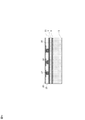
- (Semiconductor chip joint) 2 and 5T are enlarged sectional views showing an example of a joint between the semiconductor package wiring board 100 in which the semiconductor chip 4 is mounted on the semiconductor package wiring board 100 according to the present embodiment in FIG. 1 and the semiconductor chip 4. It is a figure.
- the pad portion (semiconductor chip connecting pad 14) bonded to the semiconductor chip 4 is within the recess of the insulating resin 15 within a range (depth d) of 0.3 ⁇ m or more and 5.0 ⁇ m or less, and the insulating resin around the recess. It is exposed at a position recessed from 15.
- the solder creeps up on the semiconductor chip joint portion 31 such as the copper pillar or the copper post, and the solder is covered and protected by the solder.
- the solder creeps up on the semiconductor chip joint portion 31, the semiconductor chip joint portion 31 is protected by the solder, and the contact area increases, so that the connection reliability is improved.
- the interposer 3 in order to comply with the current high-band memory (HBM) specifications, it is necessary for the interposer 3 to have a wiring width of 2 ⁇ m or more and 6 ⁇ m or less. In order to adjust the characteristic impedance to 50 ⁇ , if the wiring width is 2 ⁇ m and the wiring height is 2 ⁇ m, the insulation film thickness between the wiring is 2.5 ⁇ m, and the thickness of one layer including the wiring is 4.5 ⁇ m. .. When forming the 5-layer interposer 3 with this thickness, the interposer 3 is a very thin interposer having a total thickness of about 25 ⁇ m.
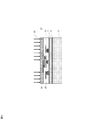
- FIG. 3A is a cross-sectional view illustrating a state in which an interposer is formed on the carrier substrate 5.
- FIG. 3B is a cross-sectional view enlarging and illustrating a part of FIG. 3A.
- the thin wiring layer 3a which is the interposer 3 is formed in a later step.
- the release layer 6 for separating from the carrier substrate 5 is formed on the carrier substrate 5 to form an interposer with a carrier substrate.
- the carrier substrate 5 a glass substrate having a surface flatness equivalent to that of a silicon wafer and a small thermal expansion coefficient can be preferably used, but the carrier substrate 5 is not limited to the glass substrate.
- the thin interposer 3 is less affected by temperature changes because the stress due to the difference in coefficient of thermal expansion (CTE: Coefficient of Thermal Expansion) is small. Therefore, the influence of the CTE difference between the FC-BGA wiring board 1 and the semiconductor chip 4 can be reduced, and the connection reliability can be improved.
- CTE Coefficient of Thermal Expansion
- the thickness of the interposer 3 is preferably 10 ⁇ m or more and 100 ⁇ m or less (preferably 20 ⁇ m or more and 50 ⁇ m or less), but if it is 1000 ⁇ m or less, the thinning effect of the semiconductor package wiring board 100 can be exhibited. In particular, the maximum effect can be exhibited when the thickness is about 10 ⁇ m to 20 ⁇ m.
- a thin interposer 3 having a thickness of 10 ⁇ m or more and 1000 ⁇ m or less can be formed for FC-BGA.
- the wiring board 1 can be flatly bonded.
- the wiring board for FC-BGA has high rigidity, and when the CTE difference with the semiconductor chip is large, the joint portion is easily broken in an environment where the temperature changes drastically such as in a heat cycle test. However, even under the same conditions, if the height of the joint is high, the joint is less likely to be broken.
- the FC-BGA wiring board 1 and the semiconductor chip 4 are joined via the thin interposer 3. Therefore, the interposer 3 serves as a buffer layer, and the CTE difference between the interposers 3 is unlikely to influence, so that high reliability can be secured.
- a glass substrate can be used as the carrier substrate 5.
- the glass substrate has excellent flatness and is suitable for forming a fine pattern on the wiring layer 3a. Further, since the glass substrate has a small CTE and is less likely to be distorted, it has excellent pattern position accuracy and flatness when bonded to the FC-BGA wiring substrate 1.
- the thickness of the glass substrate is preferably thick from the viewpoint of suppressing the occurrence of warpage in the manufacturing process, and for example, a thickness of 0.7 mm or more and 1.1 mm or less is desirable. .. Further, the usable glass substrate has a CTE of 3 ppm / ° C. or more and 15 ppm / ° C. or less, and it is particularly preferable to use a glass substrate of about 9 ppm / ° C. from the viewpoint of the CTE difference between the FC-BGA wiring substrate and the semiconductor chip. ..
- the carrier substrate 5 not an expensive silicon substrate, but a substrate such as a glass substrate which is inexpensive and has flatness equivalent to that of a silicon substrate can be used, so that the cost can be reduced.
- a wiring board to be the interposer 3 is manufactured.
- a peeling layer 6 that allows the interposer 3 to be peeled from the carrier substrate 5 is formed on one surface of the carrier substrate 5 in a later step.
- the wiring protection layer 7 is a layer for protecting the wiring layer 3a when it is peeled from the carrier substrate 5 in a later step.
- the wiring protection layer 7 is any one selected from an epoxy resin, an acrylic resin, a urethane resin, a silicon resin, a polyester resin, and an oxetane resin, or a resin in which two or more kinds selected from these resins are mixed. Any resin that can be removed after the carrier substrate 5 is peeled off may be used.
- the method for forming the wiring protection layer 7 may be appropriately selected according to the form of the resin, such as spin coating and laminating. For example, a film-shaped acrylic resin can be formed by a laminating method.
- a carrier seed layer 11 is formed on the wiring protection layer 7.
- the carrier seed layer 11 can be formed using a thin film forming technique such as a sputtering method or a vacuum deposition method.
- a thin film forming technique such as a sputtering method or a vacuum deposition method.
- the layers can be laminated in order, but the configuration and thickness may be appropriately set depending on the application.
- Ti: 50 nm and Cu: 300 nm can be stacked.
- a resist pattern 13 is formed on the carrier seed layer 11, and a semiconductor chip connection pad 14 for connection with the semiconductor chip 4 is formed in the opening 13a by electrolytic plating.
- electrolytic plating electrolytic copper plating can be preferably used, but the electrolytic plating is not limited to this.
- the wiring layer 3a to be the interposer 3 is bonded to the FC-BGA wiring substrate 1, and then the carrier substrate 5 is peeled off. After peeling the carrier substrate 5, the wiring protection layer 7 and the carrier seed layer 11 are removed to expose the semiconductor chip connection pads 14.
- the nickel layer, the gold layer, the nickel layer, the copper layer (Ni / Au / Ni / Cu) or the nickel layer is formed so that the surface of the semiconductor chip connection pad 14 becomes Au (gold).
- a layer, a gold layer, a lead layer, a nickel layer, and copper plating (Ni / Au / Pd / Ni / copper plating) are laminated in this order.
- the nickel layer is referred to as a material layer, and the other layers are referred to as metal layers. It is preferable to form Ni plating on the carrier seed layer 11 with a film thickness of 0.3 ⁇ m or more and 5.0 ⁇ m or less. By doing so, after removing the carrier substrate 5, the Ni plating is removed to form a recessed pad portion which is a recess having the insulating resin 15 as a partition in the range of 0.3 ⁇ m or more and 5.0 ⁇ m or less. be able to.
- the insulating resin 15 is formed.
- the insulating resin 15 is formed so that the semiconductor chip connecting pad 14 is embedded in the layer of the insulating resin 15.
- the insulating resin 15 is formed by a spin coating method using an epoxy resin which is a photosensitive insulating resin.
- the photosensitive epoxy resin can be cured at a relatively low temperature, and the shrinkage due to the curing (curing) after formation of the conductive via after that is small, and the step can be suppressed, and it is excellent for the subsequent fine pattern formation. There is.
- the insulating resin 15 may be formed by spin coating using a photosensitive epoxy resin, or may be formed by compression curing an insulating resin film with a vacuum laminator, and in this case, flatness is good.
- the insulating film can be formed.
- Polyimide may be used as the insulating resin as long as a slight level difference can be allowed in the exposure step.
- the conductive via 17 and the wiring 21 are formed toward the semiconductor chip connecting pad 14.
- a photosensitive epoxy resin is used for the insulating resin 15, and the removal pattern of the photosensitive epoxy resin for forming the conductive via 17 and the wiring 21 by performing UV exposure 25 (FIG. 5G) and development. Are formed (FIG. 5H).
- a vacuum deposition apparatus such as a sputtering apparatus, an ion plating apparatus, or a vacuum deposition apparatus was used.
- a film device is used to continuously form Ti and Cu to form a seed layer 18 for electrolytic plating.
- electrolytic copper plating is performed to form a copper plating film 20 on the seed layer 18.
- the copper plating film 20 is polished by CMP or surface polishing until the insulating resin 15 is exposed, and the wiring 21 connected to the conductive via 17 is formed.
- the conductive via 17 may be formed by laser light irradiation and the wiring 21 may be formed using a resist pattern.
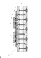
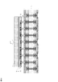
- the build-up wiring layer can be formed by repeating the wiring layer forming step shown in FIGS. 5F to 5J in accordance with the number of stacked wiring layers by using the steps described above as the wiring forming step.
- the build-up wiring layers are sequentially formed on the carrier substrate 5, one wiring 21 and the conductive via 17 in the wiring layer 3a are combined with each other in the manufacturing process, and thus the wiring board for FC-BGA is combined.
- the cross-sectional shape increases as it approaches 1 (away from the underfill 32), and the conductive via 17 has a tapered tip shape, for example.
- the conductive via 17 has a taper shape which becomes tapered as the conductive via 17 moves away from the underfill 32 (closer to the FC-BGA wiring substrate (not shown)) in the manufacturing process. It can be distinguished from the interposer 3 of the form.
- a wiring layer including a pad 27 on the interposer side that is connected to the FC-BGA wiring substrate via a protruding electrode such as a solder ball is formed.
- a solder resist layer 16 made of a heat-resistant insulating resin is formed on the outermost surface of the interposer 3 on the FC-BGA wiring substrate 1 side. As shown in FIG. 5K, the solder resist layer 16 is formed so as to cover the region including the pad 27 and the insulating resin 15.
- UV exposure 25 is performed to form the opening 16a (see FIG. 5M) at the portion where the pad 27 is exposed.
- the solder resist layer 16 is cured and stabilized by baking.
- the opening (recess) 16a is formed by developing the solder resist layer 16.
- surface treatment is performed to prevent copper from being oxidized on the surface of the pad 27 and to improve the wettability of the solder bump.
- a pad surface treatment layer 23 is formed on the surface of the pad 27 by laminating a nickel layer, a lead layer, and a gold layer (Ni / Pd / Au) in this order.
- An OSP (Organic Soilerability Preservative, surface treatment with water-soluble preflux) film may be formed on the surface of the pad 27. Further, it may be appropriately selected from electroless tin plating, nickel layer and gold layer (Ni / Au) depending on the application.
- the solder bumps 24 are formed by reflow or the like, and then the carrier substrate 5 is divided into individual pieces, whereby the interposer with the carrier substrate 5 is formed. 3 can be obtained.
- the terminals of the interposer 3 with a carrier substrate that is, the FC-BGA wiring substrate 1 designed and manufactured according to the positions of the solder bumps 24 and the interposer 3 with a carrier substrate are aligned. ..
- the FC-BGA wiring substrate 1 and the interposer 3 with the carrier substrate are joined by flip-chip mounting.
- the underfill 2 is filled in the gap formed between the interposer 3 and the FC-BGA wiring substrate 1 and is fixed by curing.
- the wiring board 1 for FC-BGA and the wiring layer 3a formed on the carrier substrate 5 to be the interposer 3 are manufactured separately, and these are bonded to each other, whereby the wiring board for the semiconductor package is manufactured. 100 has been achieved. Therefore, when the FC-BGA wiring board 1 and the wiring layer 3a (interposer 3) provided with the carrier substrate 5 are bonded together, only good products of each are selected, and the good products are bonded together to form the semiconductor package wiring board 100. To make. As a result, it is possible to achieve a high production yield and to efficiently produce the semiconductor package wiring substrate 100 without manufacturing the semiconductor package wiring substrate 100 in which either one is defective or both are defective. Is possible.
- the FC-BGA wiring board 1 and the wiring layer 3a provided with the carrier substrate 5 are joined after the respective manufacturing processes are completed, the wiring density, the number of layers, and the structure of the front and back surfaces of the substrate can be reduced. It is possible to prevent the semiconductor package wiring substrate 100 from being warped due to the difference. Furthermore, since the carrier substrate 5 is made of a material having high rigidity and low CTE and little distortion, the surface of the wiring layer 3a after the carrier substrate 5 is removed is flat, and the semiconductor chip connection pads 14 are The positional accuracy is also improved, and the semiconductor chip 4 can be easily mounted.
- the carrier substrate 5 and the peeling layer 6 are peeled together from the interposer 3.
- the wiring protection layer 7 remaining on the surface of the interposer 3 is removed.
- an alkali-soluble resin used for the wiring protection layer 7, it can be removed with an alkaline solvent (1% NaOH, 2.3% TMAH).
- the Ni plating film on the surface of the interposer 3 is removed by etching (at the same time, the nickel layer overlying the semiconductor chip connecting pad 14 is removed), and the semiconductor chip for connecting to the semiconductor chip 4 is removed.
- the Au film of the connection pad 14 is exposed.
- the wiring board 100 for semiconductor packages which is a wiring board for FC-BGA with an extremely thin interposer, is completed.
- the semiconductor chip connection pads 14 are provided in the recesses of the insulating resin 15 and are 0.3 ⁇ m or more and 5.0 ⁇ m or less from the surface. It is low in the range. That is, a structure is formed in which the insulating resin 15 serves as a partition and surrounds the semiconductor chip connecting pad 14. Therefore, the solder 30 does not spread in the direction parallel to the plane of the interposer 3 and creeps up to the semiconductor chip bonding portion 31. Therefore, it is possible to prevent the problem that the solder 30 reaches the adjacent semiconductor chip connection pads 14 and short-circuits.
- the semiconductor chip joints 31 such as the copper pillars and the copper posts are protected by the solder and also have the effect of increasing the connection area, they have a high reliability and an effect of improving the production yield. ..
- the FC-BGA wiring board 1 and the semiconductor chip 4 are bonded to each other via the interposer 3, so that the bonding distance (FC-BGA wiring board 1 and semiconductor Since the distance between the facing surfaces of the chip 4 is increased, the influence of the CTE difference can be mitigated.
- the carrier substrate 5 may be made of a metal material having a flatness with little distortion, or a ceramic substrate.
- a ceramic substrate it is easy to adjust the CTE to a desired value, and the CTE can be changed according to the constituent material of the interposer 3.
- the wiring layer 3a (interposer 3) with the carrier substrate 5 is used for FC-BGA by using a foaming resin layer that foams by heating as the peeling layer 6, for example.
- the carrier substrate 5 may be peeled from the wiring layer 3a by heating and foaming the expandable resin layer.
- the thickness of the interposer including the build-up wiring layer flip-chip mounted on the wiring board for FC-BGA via the protruding electrode is 10 ⁇ m to 1000 ⁇ m, which is very thin.
- the influence of the thermal stress due to the CTE difference of the BGA wiring board on the semiconductor package wiring board is reduced. Therefore, deformation such as warpage of the semiconductor package wiring board is small, and the semiconductor chip can be easily mounted.
- the semiconductor chip connecting pad provided in the interposer of the present embodiment is provided in the recessed portion that is recessed in the range of 0.3 ⁇ m or more and 5 ⁇ m or less from the surface of the insulating resin around the pad.
- the copper pillar is protected by the solder crawling up to the copper pillar that is the semiconductor chip joint portion 31, increasing the connection area, and in the direction parallel to the surface of the FC-BGA wiring board 1. It is possible to prevent the solder from spreading. Therefore, high reliability and high production yield can be obtained.
- the interposer is interposed between the semiconductor chip and the FC-BGA wiring board, so the distance between the two becomes large. Therefore, the stress generated between the semiconductor chip and the FC-BGA wiring board due to the CTE difference is relaxed, so that a semiconductor package having high connection reliability can be provided.
- a highly flat and rigid substrate such as a glass substrate is used as a carrier substrate, and a build-up wiring layer is formed on the carrier substrate. Since the interposer is manufactured and then flip-chip mounted on the FC-BGA wiring board, it is possible to manufacture a semiconductor package wiring board having a thin interposer having a thickness of 10 ⁇ m to 1000 ⁇ m.
- the wiring board for a semiconductor package is manufactured by manufacturing the interposer with a carrier board and the wiring board for FC-BGA in separate steps and flip-mounting them. Therefore, it becomes possible to select only non-defective products for both and to perform flip-chip mounting. Therefore, the yield of the flip-chip mounting process can be increased.
- the Au layer on the outermost surface is recessed within a range of 0.3 ⁇ m or more and 5.0 ⁇ m or less from the surface of the surrounding insulating resin. Since the pad is a recessed pad, it is possible to prevent molten solder from creeping up to a semiconductor chip bonding portion such as a copper post of a semiconductor chip when the chip is flip-chip mounted and expanding in a direction parallel to the surface of the interposer. Therefore, it is possible to prevent a short circuit between adjacent semiconductor chip joints such as copper posts due to solder. Further, since the area in which the solder contacts the semiconductor chip joint portion increases, it is possible to provide a semiconductor package with high connection reliability.
- the present invention is not limited to the above embodiment, and the application as a wiring board is considered unless the technical idea of the embodiment of the present invention deviates, It goes without saying that other layers and structures can be arbitrarily formed for the purpose of improving other required physical properties such as rigidity, strength and impact resistance.
- the present invention can be applied to a semiconductor device including a wiring board such as an interposer interposed between a semiconductor package wiring board and a semiconductor chip.
Abstract
Provided is a wiring substrate with which it is possible to suppress a decrease in the yield of an FC-BGA wiring board with an interposer and to mount a semiconductor chip well, and which has high reliability. A semiconductor packaging wiring substrate has an interposer 3 bonded to an FC-BGA wiring board 1. The interposer has a thickness of from 10 μm to 1000 μm, and a semiconductor chip-connecting pad 14 connected to the semiconductor chip 4 is provided on a surface of the interposer on the side opposite to the FC-BGA wiring board. The semiconductor chip-connecting pad is a stacked body of metal material with an Au layer on the uppermost surface thereof, wherein the surface of the Au layer is provided in a recess lower than the surface of a surrounding insulating resin 15 by a range of from 0.3 to 5.0 μm.
Description
本発明は、半導体パッケージ用配線基板とその製造方法に関する。
The present invention relates to a wiring board for a semiconductor package and a manufacturing method thereof.
近年、半導体装置の高速、高集積化が進む中で、FC-BGA(Flip Chip-Ball Grid Array)用配線基板に対しても、半導体チップと接続するための接続端子の狭ピッチ化や配線の微細化が求められている。
In recent years, with the progress of high speed and high integration of semiconductor devices, the pitch of connection terminals for connecting to a semiconductor chip and the wiring of FC-BGA (Flip Chip-Ball Grid Array) wiring boards have been reduced. Miniaturization is required.
一方、FC-BGA用配線基板とマザーボードとの接続は、従来とほぼ変わらない広めのピッチを持つ接続端子での接続が要求されている。
On the other hand, the connection between the FC-BGA wiring board and the motherboard requires connection with a connection terminal having a wide pitch that is almost the same as the conventional one.
この半導体チップと接続するための接続端子の狭ピッチ化と配線の微細化に対応するため、シリコンウェハなどを使ったシリコン基板上に配線を形成したチップ接続用の基板(シリコンインターポーザとも称す。)をFC-BGA用配線基板に接続する技術が、特許文献1に開示されている。また、FC-BGA用配線基板の表面を化学機械研磨(CMP:Chemical Mechanical Polishing)等で平坦化してから微細配線を形成する技術が、特許文献2に開示されている。
In order to cope with the narrowing of the pitch of the connection terminals for connecting to the semiconductor chip and the miniaturization of the wiring, a substrate for chip connection in which wiring is formed on a silicon substrate such as a silicon wafer (also referred to as a silicon interposer). Patent Document 1 discloses a technique for connecting a wiring board to an FC-BGA wiring board. Further, Patent Document 2 discloses a technique of forming fine wiring by flattening the surface of an FC-BGA wiring substrate by chemical mechanical polishing (CMP) or the like.
シリコンインターポーザを用いる場合、基板表面の平坦性が良好であるため微細配線を形成する上で優れている。しかしシリコンインターポーザは、シリコンウェハを使用して、半導体製造工程の前工程用の設備を用いて製造されるため、コスト高の問題が指摘されている。具体的には、シリコンウェハは形状、サイズに制限があることから、1枚のウェハから作製できるインターポーザの数が抑えられ、加えて製造設備も高価であるため、シリコンインターポーザの製造コストは一般的に高くなる。また、シリコンウェハが半導体であることから、伝送特性も劣化するという問題もある。
When using a silicon interposer, it is excellent in forming fine wiring because the flatness of the substrate surface is good. However, since the silicon interposer is manufactured by using a silicon wafer and using equipment for a pre-process of a semiconductor manufacturing process, a problem of high cost is pointed out. Specifically, since the silicon wafer has shape and size restrictions, the number of interposers that can be manufactured from a single wafer is suppressed, and the manufacturing equipment is also expensive. Therefore, the manufacturing cost of the silicon interposer is generally low. Become higher. Further, since the silicon wafer is a semiconductor, there is also a problem that the transmission characteristics are deteriorated.
これに対し、特許文献2に開示されたように、FC-BGA用配線基板の平坦化を行い、その上に微細配線層を形成する技術によれば、伝送特性劣化の問題は回避できる。しかしながら、FC-BGA用配線基板の製造歩留りに加え、難易度の高い微細配線層形成工程の歩留りが比較的低いことから、それらの掛け算となるトータルの歩留りは著しく悪いという問題がある。また、FC-BGA用配線基板の反りや歪みによる半導体チップの実装不良の問題もあった。
On the other hand, as disclosed in Patent Document 2, the technique of flattening the wiring board for FC-BGA and forming a fine wiring layer thereon can avoid the problem of transmission characteristic deterioration. However, in addition to the manufacturing yield of the FC-BGA wiring substrate, the yield in the highly difficult fine wiring layer forming step is relatively low, and therefore the total yield resulting from the multiplication is extremely poor. There is also a problem of mounting failure of the semiconductor chip due to warpage and distortion of the FC-BGA wiring board.
また、一般的な半導体チップとFC-BGA用配線基板の実装工程で、図6に示す様に、FC-BGA用配線基板に、半田30からなる突起電極によって銅ピラーなどの半導体チップ接合部31を接合する際に、半田30がFC-BGA用配線基板の面に平行方向に拡がるため、銅ピラーなどの半導体チップ接合部31と半田30の接続面積が低下するという問題がある。また、半田30が平行方向に拡がることによって隣接する半導体チップ接合部31の半田との接触により、もしくは例え接触が無い場合でもイオンマイグレーションによって短絡が生じるおそれがあった。
Further, in a mounting process of a general semiconductor chip and a wiring board for FC-BGA, as shown in FIG. 6, a semiconductor chip bonding portion 31 such as a copper pillar is formed on the wiring board for FC-BGA by a protruding electrode made of solder 30. Since the solder 30 spreads in the direction parallel to the surface of the FC-BGA wiring board when joining, there is a problem that the connection area between the semiconductor chip joining portion 31 such as a copper pillar and the solder 30 is reduced. Further, the solder 30 may spread in the parallel direction to come into contact with the solder of the adjacent semiconductor chip joint portion 31, or even if there is no contact, a short circuit may occur due to ion migration.
例えば、現在のハイバンドメモリ(HBM)の仕様に於いては、半導体チップ実装を行う側のインターポーザでは55μmピッチの狭ピッチチップ実装に対応する必要がある。狭ピッチチップ実装では熱圧着(TCB:Thermal Compression Bonding)が用いられるため、熱と圧力によって、銅ピラー上の半田はFC-BGA用配線基板の面と平行方向に拡がり(図6参照)、他の銅ピラーなどの接続部と接触し、短絡することにより、大きく収率が低下するおそれがある。
For example, according to the current high-band memory (HBM) specifications, it is necessary for the interposer on the semiconductor chip mounting side to support narrow pitch chip mounting of 55 μm pitch. Since thermal compression bonding (TCB) is used in the narrow pitch chip mounting, the solder on the copper pillar spreads in the direction parallel to the surface of the FC-BGA wiring board due to heat and pressure (see Fig. 6), etc. If the copper pillar or the like comes into contact with the connecting portion and short-circuits, the yield may be significantly reduced.
本発明は、上記問題点に鑑みてなされたものであり、半導体パッケージの収率低下を抑制し、半導体チップを良好に実装することが可能であり、且つ高い接続信頼性を兼ね備えた半導体パッケージ用配線基板及びその製造方法を提供することを課題とする。
The present invention has been made in view of the above problems, and is for a semiconductor package that suppresses a decrease in the yield of the semiconductor package, can satisfactorily mount a semiconductor chip, and has high connection reliability. An object of the present invention is to provide a wiring board and a manufacturing method thereof.
上記の課題を解決する手段として、本発明による、絶縁樹脂層と配線層とを形成したビルドアップ層からなる第2配線基板が第1配線基板に接合されてなる半導体パッケージ用配線基板において、
前記第2配線基板の厚さは10μm~1000μmであり、
前記第1配線基板と前記第2配線基板とは、前記第2配線基板の前記第1配線基板側に備えられたパッドに形成された突起電極を介して電気的に接続され、且つ両者間には絶縁性の接着剤が付与されており、
前記第2配線基板の前記第1配線基板とは反対側の面には、半導体チップと接続する半導体チップ接続用パッドと、絶縁樹脂とが備えられており、
前記半導体チップ接続用パッドは、最表面に金層を備えた金属材料からなる積層体であり、且つ前記最表面は、前記絶縁樹脂の表面に形成された凹部内で露出している。 As a means for solving the above problems, in a wiring board for a semiconductor package according to the present invention, in which a second wiring board including a buildup layer having an insulating resin layer and a wiring layer is joined to a first wiring board,
The thickness of the second wiring board is 10 μm to 1000 μm,
The first wiring board and the second wiring board are electrically connected via a protruding electrode formed on a pad provided on the side of the first wiring board of the second wiring board, and between the two. Has an insulating adhesive,
On a surface of the second wiring board opposite to the first wiring board, a semiconductor chip connection pad for connecting to a semiconductor chip and an insulating resin are provided.
The semiconductor chip connection pad is a laminated body made of a metal material having a gold layer on the outermost surface, and the outermost surface is exposed in a recess formed on the surface of the insulating resin.
本発明によれば、半導体パッケージの収率低下を抑制し、半導体チップを良好に実装することが可能であり、且つ高い接続信頼性を兼ね備えた半導体パッケージ用配線基板及びその製造方法を提供することが可能になる。
According to the present invention, it is possible to provide a wiring board for a semiconductor package, which can suppress a decrease in the yield of the semiconductor package, can satisfactorily mount a semiconductor chip, and have high connection reliability, and a manufacturing method thereof. Will be possible.
以下に、本発明の一実施形態に係る配線基板について図面を参照して説明する。ただし、以下に説明する各図において相互に対応する部分については同一符号を付し、重複部分においては説明を適宜省略する。また、各図面は説明を容易にするために適宜誇張して表現している場合がある。
さらに、本発明の一実施形態は、本発明の技術的思想を具体化するための構成を例示するものであって、各部の材質、形状、構造、配置等を下記のものに特定するものでない。本発明の技術的思想は、特許請求の範囲に記載された請求項が規定する技術的範囲内において、適宜変更を加えることができる。 A wiring board according to an embodiment of the present invention will be described below with reference to the drawings. However, in each of the drawings described below, portions corresponding to each other are designated by the same reference numerals, and description of overlapping portions will be appropriately omitted. In addition, each drawing may be exaggerated as appropriate for ease of explanation.
Furthermore, one embodiment of the present invention exemplifies a configuration for embodying the technical idea of the present invention, and does not specify the material, shape, structure, arrangement, etc. of each part as follows. .. The technical idea of the present invention can be appropriately modified within the technical scope defined by the claims described in the claims.
<半導体パッケージ用配線基板>
以下、図面を参照しつつ、本発明の半導体パッケージ用配線基板の実施形態を説明する。 <Wiring board for semiconductor package>
Hereinafter, an embodiment of a wiring board for a semiconductor package of the present invention will be described with reference to the drawings.
以下、図面を参照しつつ、本発明の半導体パッケージ用配線基板の実施形態を説明する。 <Wiring board for semiconductor package>
Hereinafter, an embodiment of a wiring board for a semiconductor package of the present invention will be described with reference to the drawings.
(半導体パッケージ)
まず、本実施形態の半導体パッケージ用配線基板に半導体チップを実装した半導体パッケージについて説明する。
図1は、半導体パッケージ用配線基板100に半導体チップ4を実装した半導体パッケージ50の一例を示す断面図である。 (Semiconductor package)
First, a semiconductor package in which a semiconductor chip is mounted on the semiconductor package wiring board of the present embodiment will be described.
FIG. 1 is a sectional view showing an example of asemiconductor package 50 in which a semiconductor chip 4 is mounted on a semiconductor package wiring board 100.
まず、本実施形態の半導体パッケージ用配線基板に半導体チップを実装した半導体パッケージについて説明する。
図1は、半導体パッケージ用配線基板100に半導体チップ4を実装した半導体パッケージ50の一例を示す断面図である。 (Semiconductor package)
First, a semiconductor package in which a semiconductor chip is mounted on the semiconductor package wiring board of the present embodiment will be described.
FIG. 1 is a sectional view showing an example of a
本発明の一実施形態に係る半導体パッケージ50は、FC-BGA用配線基板(第1配線基板ともいう)1の一方の面に、樹脂層と配線層が交互に積層されてなるビルドアップ配線層(ビルドアップ層ともいう)のみで形成された微細配線層を備えた薄いインターポーザ(第2配線基板ともいう)3が、半田バンプ24または銅ポスト(銅ピラー)または金バンプなどの突起電極を介して接合されている。また、FC-BGA用配線基板1とインターポーザ3との隙間には、絶縁性樹脂からなる接着剤であるインターポーザ用アンダーフィル2が充填されて硬化している。さらにインターポーザ3の、FC-BGA用配線基板1とは逆側の面に、半導体チップ4が銅ピラーなどからなる半導体チップ接合部31を介して接合され、半導体チップ4とインターポーザ3との隙間には、絶縁性樹脂からなる接着剤である半導体チップ用アンダーフィル32が充填されて硬化している。
A semiconductor package 50 according to an embodiment of the present invention is a build-up wiring layer in which a resin layer and a wiring layer are alternately laminated on one surface of an FC-BGA wiring substrate (also referred to as a first wiring substrate) 1. A thin interposer (also referred to as a second wiring substrate) 3 having a fine wiring layer formed only by (also referred to as a build-up layer) 3 via a bump electrode such as a solder bump 24 or a copper post (copper pillar) or a gold bump. Are joined together. An interposer underfill 2, which is an adhesive made of an insulating resin, is filled in the gap between the FC-BGA wiring board 1 and the interposer 3 and is cured. Further, the semiconductor chip 4 is bonded to the surface of the interposer 3 opposite to the FC-BGA wiring substrate 1 via the semiconductor chip bonding portion 31 made of a copper pillar or the like, and in the gap between the semiconductor chip 4 and the interposer 3. Is filled and cured with an underfill 32 for a semiconductor chip, which is an adhesive made of an insulating resin.
本実施形態の半導体パッケージ用配線基板100では、図2に示すように、半導体チップ接続用パッド14は、その表面にAu(金)層が設けられ、且つ絶縁樹脂15の周囲表面に設けられた凹部内にて露出しており、凹部の周囲の表面より0.3μm以上、5.0μm以下(好ましくは、0.5μm以上、3.0μm以下)の範囲(深さd)で凹んだパッド部となる。この半導体パッケージ用配線基板100のインターポーザ3側は、半導体チップ4の半導体チップ接合部31である銅ピラー、銅ポストなどを介して接続される。また、半導体チップ接続用パッド14と半導体チップ4の隙間にアンダーフィル32を充填し、硬化させることによって、図1に示すような半導体パッケージ50を得ることができる。
In the semiconductor package wiring board 100 of the present embodiment, as shown in FIG. 2, the semiconductor chip connection pad 14 is provided with an Au (gold) layer on its surface and is provided on the peripheral surface of the insulating resin 15. A pad portion that is exposed in the recess and is recessed in the range (depth d) of 0.3 μm or more and 5.0 μm or less (preferably 0.5 μm or more and 3.0 μm or less) from the surface around the recess. Becomes The interposer 3 side of the semiconductor package wiring substrate 100 is connected via a copper pillar, a copper post, or the like, which is the semiconductor chip bonding portion 31 of the semiconductor chip 4. Further, by filling the gap between the semiconductor chip connecting pad 14 and the semiconductor chip 4 with the underfill 32 and curing the same, the semiconductor package 50 as shown in FIG. 1 can be obtained.
(アンダーフィル)
アンダーフィル2は、FC-BGA用配線基板1とインターポーザ3とを固定及び封止するために用いられる接着材料である。アンダーフィル2としては、例えば、エポキシ樹脂、ウレタン樹脂、シリコン樹脂、ポリエステル樹脂、オキセタン樹脂、及びマレイミド樹脂の1種又はこれらの樹脂の2種類以上が混合された樹脂に、フィラーとしてのシリカ、酸化チタン、酸化アルミニウム、酸化マグネシウム、又は酸化亜鉛等が加えられた材料が用いられる。アンダーフィル2は、液状の樹脂を充填させることで形成してもよい。また、アンダーフィル2の代わりに絶縁性の接着部材として異方性導電フィルム(ACF)、または接着及び絶縁の機能を同時に持つフィルム状接続材料(NCF)を用いることでFC-BGA用配線基板1とインターポーザ3とを固定し、これら隙間を封止してもよい。 (Underfill)
Theunderfill 2 is an adhesive material used to fix and seal the FC-BGA wiring board 1 and the interposer 3. As the underfill 2, for example, epoxy resin, urethane resin, silicon resin, polyester resin, oxetane resin, and maleimide resin, or a resin in which two or more kinds of these resins are mixed, silica as a filler, oxidation A material to which titanium, aluminum oxide, magnesium oxide, zinc oxide, or the like is added is used. The underfill 2 may be formed by filling a liquid resin. Further, by using an anisotropic conductive film (ACF) as an insulating adhesive member instead of the underfill 2 or a film-like connecting material (NCF) having the functions of adhesion and insulation at the same time, the wiring board for FC-BGA 1 And the interposer 3 may be fixed and these gaps may be sealed.
アンダーフィル2は、FC-BGA用配線基板1とインターポーザ3とを固定及び封止するために用いられる接着材料である。アンダーフィル2としては、例えば、エポキシ樹脂、ウレタン樹脂、シリコン樹脂、ポリエステル樹脂、オキセタン樹脂、及びマレイミド樹脂の1種又はこれらの樹脂の2種類以上が混合された樹脂に、フィラーとしてのシリカ、酸化チタン、酸化アルミニウム、酸化マグネシウム、又は酸化亜鉛等が加えられた材料が用いられる。アンダーフィル2は、液状の樹脂を充填させることで形成してもよい。また、アンダーフィル2の代わりに絶縁性の接着部材として異方性導電フィルム(ACF)、または接着及び絶縁の機能を同時に持つフィルム状接続材料(NCF)を用いることでFC-BGA用配線基板1とインターポーザ3とを固定し、これら隙間を封止してもよい。 (Underfill)
The
アンダーフィル32は、半導体チップ4とインターポーザ3とを固定及び封止するために用いられる接着剤であり、アンダーフィル2と同様の材料で構成される。なお、この場合も、アンダーフィル32の代わりに、異方性導電フィルム(ACF)または、フィルム状接続材料(NCF)を用いてもよい。
The underfill 32 is an adhesive used to fix and seal the semiconductor chip 4 and the interposer 3, and is made of the same material as the underfill 2. In this case as well, the anisotropic conductive film (ACF) or the film-like connecting material (NCF) may be used instead of the underfill 32.
(インターポーザの配線ピッチ)
インターポーザ3における半導体チップ4と接合される部分の配線ピッチは、半導体チップ4とFC-BGA用配線基板1とを直接接合する場合の、FC-BGA用配線基板1における半導体チップ4と接合される部分の配線ピッチよりも狭くなっている。すなわち、インターポーザ3の半導体チップ4を実装する面における配線ピッチは、FC-BGA用配線基板1に半導体チップ4を直接的に接合する場合のFC-BGA用配線基板1の配線ピッチより微細な配線となっている。 (Interposer wiring pitch)
The wiring pitch of the portion of theinterposer 3 that is joined to the semiconductor chip 4 is joined to the semiconductor chip 4 of the FC-BGA wiring substrate 1 when the semiconductor chip 4 and the FC-BGA wiring substrate 1 are directly joined. It is narrower than the part wiring pitch. That is, the wiring pitch on the surface of the interposer 3 on which the semiconductor chip 4 is mounted is finer than the wiring pitch of the FC-BGA wiring board 1 when the semiconductor chip 4 is directly bonded to the FC-BGA wiring board 1. Has become.
インターポーザ3における半導体チップ4と接合される部分の配線ピッチは、半導体チップ4とFC-BGA用配線基板1とを直接接合する場合の、FC-BGA用配線基板1における半導体チップ4と接合される部分の配線ピッチよりも狭くなっている。すなわち、インターポーザ3の半導体チップ4を実装する面における配線ピッチは、FC-BGA用配線基板1に半導体チップ4を直接的に接合する場合のFC-BGA用配線基板1の配線ピッチより微細な配線となっている。 (Interposer wiring pitch)
The wiring pitch of the portion of the
(半導体チップ接合部)
図2および図5Tは、図1における本実施形態に係る半導体パッケージ用配線基板100に半導体チップ4を実装した半導体パッケージ用配線基板100と半導体チップ4との接合部の一例を拡大して示す断面図である。半導体チップ4と接合されるパッド部(半導体チップ接続用パッド14)は、絶縁樹脂15の凹部内において、0.3μm以上、5.0μm以下の範囲(深さd)で、凹部周囲の絶縁樹脂15より凹んだ位置で露出している。このため、半導体チップ4を実装したときに、銅ピラーや銅ポストなどの半導体チップ接合部31を半田が這い上がり、これが半田によって被覆され、保護される。半導体チップ接合部31を半田が這い上がり、半導体チップ接合部31が半田によって保護され、また接触面積が増加するため、接続信頼性が向上する。また、FC-BGA用配線基板1の面と平行な方向に半田が拡がって行く事を抑制することができるため、隣接する半導体チップ接合部31間の短絡事象が抑制され、高い生産歩留りを実現する事ができる。 (Semiconductor chip joint)
2 and 5T are enlarged sectional views showing an example of a joint between the semiconductorpackage wiring board 100 in which the semiconductor chip 4 is mounted on the semiconductor package wiring board 100 according to the present embodiment in FIG. 1 and the semiconductor chip 4. It is a figure. The pad portion (semiconductor chip connecting pad 14) bonded to the semiconductor chip 4 is within the recess of the insulating resin 15 within a range (depth d) of 0.3 μm or more and 5.0 μm or less, and the insulating resin around the recess. It is exposed at a position recessed from 15. Therefore, when the semiconductor chip 4 is mounted, the solder creeps up on the semiconductor chip joint portion 31 such as the copper pillar or the copper post, and the solder is covered and protected by the solder. The solder creeps up on the semiconductor chip joint portion 31, the semiconductor chip joint portion 31 is protected by the solder, and the contact area increases, so that the connection reliability is improved. Further, since it is possible to prevent the solder from spreading in the direction parallel to the surface of the FC-BGA wiring board 1, a short-circuit phenomenon between the adjacent semiconductor chip joints 31 is suppressed, and a high production yield is realized. You can do it.
図2および図5Tは、図1における本実施形態に係る半導体パッケージ用配線基板100に半導体チップ4を実装した半導体パッケージ用配線基板100と半導体チップ4との接合部の一例を拡大して示す断面図である。半導体チップ4と接合されるパッド部(半導体チップ接続用パッド14)は、絶縁樹脂15の凹部内において、0.3μm以上、5.0μm以下の範囲(深さd)で、凹部周囲の絶縁樹脂15より凹んだ位置で露出している。このため、半導体チップ4を実装したときに、銅ピラーや銅ポストなどの半導体チップ接合部31を半田が這い上がり、これが半田によって被覆され、保護される。半導体チップ接合部31を半田が這い上がり、半導体チップ接合部31が半田によって保護され、また接触面積が増加するため、接続信頼性が向上する。また、FC-BGA用配線基板1の面と平行な方向に半田が拡がって行く事を抑制することができるため、隣接する半導体チップ接合部31間の短絡事象が抑制され、高い生産歩留りを実現する事ができる。 (Semiconductor chip joint)
2 and 5T are enlarged sectional views showing an example of a joint between the semiconductor
例えば、現在のハイバンドメモリ(HBM)の仕様に対応するためには、インターポーザ3では配線幅を2μm以上、6μm以下にする必要がある。特性インピーダンスを50Ωに合わせるためには、配線幅を2μm、配線高さを2μmとすると、配線間の絶縁膜厚は2.5μmとなり、配線も含めた1層の厚さは4.5μmとなる。この厚さで5層のインターポーザ3を形成する場合、インターポーザ3は、総厚25μm程度と非常に薄いインターポーザとなる。
For example, in order to comply with the current high-band memory (HBM) specifications, it is necessary for the interposer 3 to have a wiring width of 2 μm or more and 6 μm or less. In order to adjust the characteristic impedance to 50Ω, if the wiring width is 2 μm and the wiring height is 2 μm, the insulation film thickness between the wiring is 2.5 μm, and the thickness of one layer including the wiring is 4.5 μm. .. When forming the 5-layer interposer 3 with this thickness, the interposer 3 is a very thin interposer having a total thickness of about 25 μm.
(キャリア基板付きインターポーザ)
図3Aは、キャリア基板5上に、インターポーザを形成した状態を例示した断面図である。図3Bは、図3Aの一部を拡大して例示した断面図である。
図3Bに示すように、非常に薄いインターポーザ3とFC-BGA用配線基板1との接合を、平坦性を確保した状態で行うためには、インターポーザ3である薄い配線層3aを、後工程でキャリア基板5から分離するための剥離層6を形成したキャリア基板5上に形成し、キャリア基板付きインターポーザとする。キャリア基板5は、その表面の平坦性がシリコンウェハと同等レベルであり、熱膨張係数も小さいガラス基板を好適に使用することができるが、ガラス基板に限定する必要はない。 (Interposer with carrier board)
FIG. 3A is a cross-sectional view illustrating a state in which an interposer is formed on thecarrier substrate 5. FIG. 3B is a cross-sectional view enlarging and illustrating a part of FIG. 3A.
As shown in FIG. 3B, in order to bond the verythin interposer 3 and the FC-BGA wiring substrate 1 in a state where the flatness is ensured, the thin wiring layer 3a which is the interposer 3 is formed in a later step. The release layer 6 for separating from the carrier substrate 5 is formed on the carrier substrate 5 to form an interposer with a carrier substrate. As the carrier substrate 5, a glass substrate having a surface flatness equivalent to that of a silicon wafer and a small thermal expansion coefficient can be preferably used, but the carrier substrate 5 is not limited to the glass substrate.
図3Aは、キャリア基板5上に、インターポーザを形成した状態を例示した断面図である。図3Bは、図3Aの一部を拡大して例示した断面図である。
図3Bに示すように、非常に薄いインターポーザ3とFC-BGA用配線基板1との接合を、平坦性を確保した状態で行うためには、インターポーザ3である薄い配線層3aを、後工程でキャリア基板5から分離するための剥離層6を形成したキャリア基板5上に形成し、キャリア基板付きインターポーザとする。キャリア基板5は、その表面の平坦性がシリコンウェハと同等レベルであり、熱膨張係数も小さいガラス基板を好適に使用することができるが、ガラス基板に限定する必要はない。 (Interposer with carrier board)
FIG. 3A is a cross-sectional view illustrating a state in which an interposer is formed on the
As shown in FIG. 3B, in order to bond the very
また、厚さが薄いインターポーザ3は、熱膨張率(CTE:Coefficient of Thermal Expansion)差による応力が小さいため、温度変化の影響は少ない。そのため、FC-BGA用配線基板1と半導体チップ4とのCTE差による影響を低減し、接続信頼性を向上させることができる。
Also, the thin interposer 3 is less affected by temperature changes because the stress due to the difference in coefficient of thermal expansion (CTE: Coefficient of Thermal Expansion) is small. Therefore, the influence of the CTE difference between the FC-BGA wiring board 1 and the semiconductor chip 4 can be reduced, and the connection reliability can be improved.
また、インターポーザ3は、厚さ10μm以上、100μm以下(好ましくは20μm以上、50μm以下)が好ましいが、1000μm以下であれば、半導体パッケージ用配線基板100の薄形効果を発揮することができる。特に厚さ10μmから20μm程度で最も効果を発揮することができる。
The thickness of the interposer 3 is preferably 10 μm or more and 100 μm or less (preferably 20 μm or more and 50 μm or less), but if it is 1000 μm or less, the thinning effect of the semiconductor package wiring board 100 can be exhibited. In particular, the maximum effect can be exhibited when the thickness is about 10 μm to 20 μm.
(半導体パッケージ用配線基板)
キャリア基板5に形成されたインターポーザ3を、別に用意したFC-BGA用配線基板1にフリップチップ実装した後、FC-BGA用配線基板1とインターポーザ3との隙間にアンダーフィル2を充填し、硬化させる。次に、図4に示す様に、キャリア基板5をインターポーザ3から取り除き、インターポーザ3の配線層3aに形成された半導体チップ4との接合用の半導体チップ接続用パッド14を露出させる。次に、半導体チップ接続用パッド14の最上層のNi層(厚さ0.3μm以上、5.0μm以下)を除去することで、0.3μm以上、5.0μm以下の凹みを備えたパッド部(半導体チップ接続用パッド14)を形成することができる。更に、そのパッド部に半田バンプなどの突起電極を形成することによって、本実施形態に係る半導体パッケージ用配線基板100が形成される。 (Wiring board for semiconductor package)
After theinterposer 3 formed on the carrier substrate 5 is flip-chip mounted on a separately prepared FC-BGA wiring substrate 1, an underfill 2 is filled in the gap between the FC-BGA wiring substrate 1 and the interposer 3 and cured. Let Next, as shown in FIG. 4, the carrier substrate 5 is removed from the interposer 3 to expose the semiconductor chip connection pads 14 for joining with the semiconductor chip 4 formed on the wiring layer 3a of the interposer 3. Next, the uppermost Ni layer (thickness 0.3 μm or more and 5.0 μm or less) of the semiconductor chip connecting pad 14 is removed to provide a pad portion having a recess of 0.3 μm or more and 5.0 μm or less. (Pad 14 for semiconductor chip connection) can be formed. Further, by forming a protruding electrode such as a solder bump on the pad portion, the semiconductor package wiring board 100 according to the present embodiment is formed.
キャリア基板5に形成されたインターポーザ3を、別に用意したFC-BGA用配線基板1にフリップチップ実装した後、FC-BGA用配線基板1とインターポーザ3との隙間にアンダーフィル2を充填し、硬化させる。次に、図4に示す様に、キャリア基板5をインターポーザ3から取り除き、インターポーザ3の配線層3aに形成された半導体チップ4との接合用の半導体チップ接続用パッド14を露出させる。次に、半導体チップ接続用パッド14の最上層のNi層(厚さ0.3μm以上、5.0μm以下)を除去することで、0.3μm以上、5.0μm以下の凹みを備えたパッド部(半導体チップ接続用パッド14)を形成することができる。更に、そのパッド部に半田バンプなどの突起電極を形成することによって、本実施形態に係る半導体パッケージ用配線基板100が形成される。 (Wiring board for semiconductor package)
After the
上記手順で、厚さ10μm以上、1000μm以下の配線層3aからなるインターポーザ3をFC-BGA用配線基板1に接合することによって、厚さ10μm以上、1000μm以下の薄いインターポーザ3を、FC-BGA用配線基板1に平坦に接合することができる。
By joining the interposer 3 composed of the wiring layer 3a having a thickness of 10 μm or more and 1000 μm or less to the FC-BGA wiring board 1 by the above procedure, a thin interposer 3 having a thickness of 10 μm or more and 1000 μm or less can be formed for FC-BGA. The wiring board 1 can be flatly bonded.
一般的にFC-BGA用配線基板は高剛性を備えており、半導体チップとのCTE差が大きい場合には、ヒートサイクル試験などの激しく温度が変化する環境下において、接合部が破壊され易い。しかし、同条件でも接合部の高さが高ければ、接合部が破壊されにくくなるという性質がある。
Generally, the wiring board for FC-BGA has high rigidity, and when the CTE difference with the semiconductor chip is large, the joint portion is easily broken in an environment where the temperature changes drastically such as in a heat cycle test. However, even under the same conditions, if the height of the joint is high, the joint is less likely to be broken.
本実施形態に係る半導体パッケージ用配線基板100では、FC-BGA用配線基板1と、半導体チップ4とは、薄いインターポーザ3を介して接合されている。そのため、インターポーザ3が緩衝層となり、お互いのCTE差が影響しにくくなり、高い信頼性を確保することができる。
In the semiconductor package wiring board 100 according to the present embodiment, the FC-BGA wiring board 1 and the semiconductor chip 4 are joined via the thin interposer 3. Therefore, the interposer 3 serves as a buffer layer, and the CTE difference between the interposers 3 is unlikely to influence, so that high reliability can be secured.
<半導体パッケージ用配線基板の製造方法>
次に図5A~5Tを参照して、本実施形態に係るインターポーザ3を備えた半導体パッケージ用配線基板100の製造工程の一例を説明する。 <Method of manufacturing wiring board for semiconductor package>
Next, with reference to FIGS. 5A to 5T, an example of a manufacturing process of the semiconductorpackage wiring board 100 including the interposer 3 according to the present embodiment will be described.
次に図5A~5Tを参照して、本実施形態に係るインターポーザ3を備えた半導体パッケージ用配線基板100の製造工程の一例を説明する。 <Method of manufacturing wiring board for semiconductor package>
Next, with reference to FIGS. 5A to 5T, an example of a manufacturing process of the semiconductor
本実施形態においては、キャリア基板5として、例えばガラス基板を用いることができる。ガラス基板は平坦性に優れており、配線層3aの微細なパターン形成に適している。また、ガラス基板はCTEが小さく歪みにくいことから、FC-BGA用配線基板1と接合した時のパターン位置精度及び平坦性に優れている。
In this embodiment, for example, a glass substrate can be used as the carrier substrate 5. The glass substrate has excellent flatness and is suitable for forming a fine pattern on the wiring layer 3a. Further, since the glass substrate has a small CTE and is less likely to be distorted, it has excellent pattern position accuracy and flatness when bonded to the FC-BGA wiring substrate 1.
また、キャリア基板5としてガラス基板を用いる場合、ガラス基板の厚さは、製造プロセスにおける反りの発生を抑制する観点から厚い方が望ましく、例えば0.7mm以上、1.1mm以下程度の厚みが望ましい。また、使用可能なガラス基板のCTEは3ppm/℃以上、15ppm/℃以下であり、特にFC-BGA用配線基板、半導体チップのCTE差の観点から、9ppm/℃程度のガラス基板を用いると望ましい。
When a glass substrate is used as the carrier substrate 5, the thickness of the glass substrate is preferably thick from the viewpoint of suppressing the occurrence of warpage in the manufacturing process, and for example, a thickness of 0.7 mm or more and 1.1 mm or less is desirable. .. Further, the usable glass substrate has a CTE of 3 ppm / ° C. or more and 15 ppm / ° C. or less, and it is particularly preferable to use a glass substrate of about 9 ppm / ° C. from the viewpoint of the CTE difference between the FC-BGA wiring substrate and the semiconductor chip. ..
また、キャリア基板5として、高価なシリコン基板ではなく、ガラス基板をはじめとした安価でシリコン基板並みの平坦性を備えた基板を利用することができるため、コスト削減を図ることができる。
Further, as the carrier substrate 5, not an expensive silicon substrate, but a substrate such as a glass substrate which is inexpensive and has flatness equivalent to that of a silicon substrate can be used, so that the cost can be reduced.
図5Aに示す様に、インターポーザ3となる配線基板を作製する。まず、キャリア基板5の一方の面に、後工程で、インターポーザ3をキャリア基板5から剥離可能とする剥離層6を形成する。
As shown in FIG. 5A, a wiring board to be the interposer 3 is manufactured. First, a peeling layer 6 that allows the interposer 3 to be peeled from the carrier substrate 5 is formed on one surface of the carrier substrate 5 in a later step.
次いで、図5Bに示す様に、剥離層6の上に配線保護層7を形成する。配線保護層7は、後工程でキャリア基板5から剥離する際に配線層3aを保護するための層である。配線保護層7は、エポキシ樹脂、アクリル樹脂、ウレタン樹脂、シリコン樹脂、ポリエステル樹脂、オキセタン樹脂の中から選択したいずれか1種又はこれらの樹脂から選択された2種類以上が混合された樹脂であり、キャリア基板5を剥離後に除去可能な樹脂であれば良い。配線保護層7の形成方法については、スピンコート、ラミネート等、樹脂の形態に応じて適宜選択すればよい。例えば、フィルム状のアクリル系樹脂を、ラミネート法を用いて形成することができる。
Next, as shown in FIG. 5B, the wiring protection layer 7 is formed on the peeling layer 6. The wiring protection layer 7 is a layer for protecting the wiring layer 3a when it is peeled from the carrier substrate 5 in a later step. The wiring protection layer 7 is any one selected from an epoxy resin, an acrylic resin, a urethane resin, a silicon resin, a polyester resin, and an oxetane resin, or a resin in which two or more kinds selected from these resins are mixed. Any resin that can be removed after the carrier substrate 5 is peeled off may be used. The method for forming the wiring protection layer 7 may be appropriately selected according to the form of the resin, such as spin coating and laminating. For example, a film-shaped acrylic resin can be formed by a laminating method.
次いで、図5Cに示す様に、配線保護層7上にキャリアシード層11を形成する。キャリアシード層11は、スパッタ法や真空蒸着法などの薄膜形成技術を用いて形成することができる。キャリアシード層11の構成については、チタン層と銅層(Ti/Cu)、クロム層と銅層(Cr/Cu)、ニッケルクロム層と銅層(NiCr/Cu)等、配線保護層7からこの順序で積層することができるが、用途に応じて適宜構成や厚みを設定して構わない。一例として、Ti:50nm、Cu:300nmを積層することができる。配線保護層7上にキャリアシード層11を形成することで、この上に電解銅めっきなどが可能となる。
Next, as shown in FIG. 5C, a carrier seed layer 11 is formed on the wiring protection layer 7. The carrier seed layer 11 can be formed using a thin film forming technique such as a sputtering method or a vacuum deposition method. Regarding the structure of the carrier seed layer 11, the titanium layer and the copper layer (Ti / Cu), the chromium layer and the copper layer (Cr / Cu), the nickel chrome layer and the copper layer (NiCr / Cu), etc. The layers can be laminated in order, but the configuration and thickness may be appropriately set depending on the application. As an example, Ti: 50 nm and Cu: 300 nm can be stacked. By forming the carrier seed layer 11 on the wiring protection layer 7, electrolytic copper plating or the like can be performed thereon.
次に図5Dに示すように、キャリアシード層11上にレジストパターン13を形成し、その開口部13aに電解めっきにより半導体チップ4との接続用の半導体チップ接続用パッド14を形成する。電解めっきとしては、電解銅めっきを好適に使用する事ができるが、これに限定する必要はない。
Next, as shown in FIG. 5D, a resist pattern 13 is formed on the carrier seed layer 11, and a semiconductor chip connection pad 14 for connection with the semiconductor chip 4 is formed in the opening 13a by electrolytic plating. As the electrolytic plating, electrolytic copper plating can be preferably used, but the electrolytic plating is not limited to this.
図3Bおよび図4に示すように、インターポーザ3となる配線層3aをFC-BGA用配線基板1と接合した後、キャリア基板5を剥離する。キャリア基板5の剥離後に、配線保護層7とキャリアシード層11を除去する事により、半導体チップ接続用パッド14を露出させる。この状態で、半導体チップ接続用パッド14の表面がAu(金)となるように、キャリアシード層11から、ニッケル層、金層、ニッケル層、銅層(Ni/Au/Ni/Cu)またはニッケル層、金層、鉛層、ニッケル層、銅めっき(Ni/Au/Pd/Ni/銅めっき)の順に積層して形成する。ニッケル層を材料層とし、それ以外を金属層という。キャリアシード層11上にNiめっきを0.3μm以上、5.0μm以下の膜厚で形成する事が好ましい。そうする事により、キャリア基板5を剥離後、そのNiめっきを除去することで、0.3μm以上、5.0μm以下の範囲で、絶縁樹脂15を隔壁とした凹みである凹みパッド部を形成することができる。
As shown in FIGS. 3B and 4, the wiring layer 3a to be the interposer 3 is bonded to the FC-BGA wiring substrate 1, and then the carrier substrate 5 is peeled off. After peeling the carrier substrate 5, the wiring protection layer 7 and the carrier seed layer 11 are removed to expose the semiconductor chip connection pads 14. In this state, from the carrier seed layer 11, the nickel layer, the gold layer, the nickel layer, the copper layer (Ni / Au / Ni / Cu) or the nickel layer is formed so that the surface of the semiconductor chip connection pad 14 becomes Au (gold). A layer, a gold layer, a lead layer, a nickel layer, and copper plating (Ni / Au / Pd / Ni / copper plating) are laminated in this order. The nickel layer is referred to as a material layer, and the other layers are referred to as metal layers. It is preferable to form Ni plating on the carrier seed layer 11 with a film thickness of 0.3 μm or more and 5.0 μm or less. By doing so, after removing the carrier substrate 5, the Ni plating is removed to form a recessed pad portion which is a recess having the insulating resin 15 as a partition in the range of 0.3 μm or more and 5.0 μm or less. be able to.
その後、図5Eに示す様にレジストパターン13を除去する。
After that, the resist pattern 13 is removed as shown in FIG. 5E.
次に、図5Fに示す様に、絶縁樹脂15を形成する。絶縁樹脂15は半導体チップ接続用パッド14が絶縁樹脂15の層内に埋没するように形成する。本実施形態では、絶縁樹脂15を、感光性絶縁樹脂のエポキシ系樹脂をもちいてスピンコート法により形成する。感光性エポキシ樹脂は比較的低温で硬化することができ、この後の導通ビア形成後のキュア(硬化)による収縮が少なく、段差を抑えることが可能であり、さらにその後の微細パターン形成に優れている。絶縁樹脂15としては、感光性のエポキシ系樹脂を用いてスピンコート法により形成する他、絶縁樹脂フィルムを真空ラミネータで圧縮キュアを行って形成することも可能であり、この場合は平坦性の良い絶縁膜を形勢することができる。露光工程で多少の段差が許容できるのであれば、ポリイミドを絶縁樹脂として用いても良い。
Next, as shown in FIG. 5F, the insulating resin 15 is formed. The insulating resin 15 is formed so that the semiconductor chip connecting pad 14 is embedded in the layer of the insulating resin 15. In this embodiment, the insulating resin 15 is formed by a spin coating method using an epoxy resin which is a photosensitive insulating resin. The photosensitive epoxy resin can be cured at a relatively low temperature, and the shrinkage due to the curing (curing) after formation of the conductive via after that is small, and the step can be suppressed, and it is excellent for the subsequent fine pattern formation. There is. The insulating resin 15 may be formed by spin coating using a photosensitive epoxy resin, or may be formed by compression curing an insulating resin film with a vacuum laminator, and in this case, flatness is good. The insulating film can be formed. Polyimide may be used as the insulating resin as long as a slight level difference can be allowed in the exposure step.
次に、図5G,5Hに示すように、半導体チップ接続用パッド14に向かって導通ビア17と配線21を形成する。ここでは絶縁樹脂15に感光性エポキシ系樹脂を使用しており、UV露光25(図5G)及び現像を行うことにより、導通ビア17と配線21を形成するための感光性エポキシ系樹脂の除去パターンを形成する(図5H)。
Next, as shown in FIGS. 5G and 5H, the conductive via 17 and the wiring 21 are formed toward the semiconductor chip connecting pad 14. Here, a photosensitive epoxy resin is used for the insulating resin 15, and the removal pattern of the photosensitive epoxy resin for forming the conductive via 17 and the wiring 21 by performing UV exposure 25 (FIG. 5G) and development. Are formed (FIG. 5H).
その後、図5Iに示すように、酸素プラズマアッシング等で感光性エポキシ系樹脂が現像によって除去された部位における樹脂の残渣を除去した後、スパッタ装置、イオンプレーティング装置、真空蒸着装置などの真空成膜装置を用いてTiとCuを連続で成膜し、電解めっきのシード層18を形成する。次に電解銅めっき処理を行い、シード層18の上に銅めっき膜20を形成する。
Then, as shown in FIG. 5I, after removing the residue of the resin at the portion where the photosensitive epoxy resin was removed by development by oxygen plasma ashing or the like, a vacuum deposition apparatus such as a sputtering apparatus, an ion plating apparatus, or a vacuum deposition apparatus was used. A film device is used to continuously form Ti and Cu to form a seed layer 18 for electrolytic plating. Next, electrolytic copper plating is performed to form a copper plating film 20 on the seed layer 18.
その後、図5Jに示すように、CMPもしくは表面研磨により絶縁樹脂15が露出するまで銅めっき膜20を研磨し、導通ビア17と接続した配線21を形成する。
絶縁樹脂15にフィルム状樹脂やポリイミドを使用する場合、レーザ光照射によって導通ビア17を形成し、レジストパターンを用いて配線21を形成してもかまわない。
以上説明した工程を配線形成工程とし、積み重ね配線層数に合わせて、図5F~図5Jに示した配線層の形成工程を繰り返すことにより、ビルドアップ配線層を形成することができる。
本実施形態によれば、キャリア基板5に対してビルドアップ配線層を順次形成しているため、製造工程上、配線層3aにおける一つの配線21及び導通ビア17では、組み合わせるFC-BGA用配線基板1に接近する(アンダーフィル32から遠ざかる)にしたがってその断面形状が大きくなり、例えば導通ビア17は先太テーパ形状となる。これに対し、図6の構成では、製造工程上、導通ビア17がアンダーフィル32から離れる(不図示のFC-BGA用配線基板に近づく)に従って先細となるテーパ形状であり、この点で本実施形態のインターポーザ3とは区別できる。 Thereafter, as shown in FIG. 5J, thecopper plating film 20 is polished by CMP or surface polishing until the insulating resin 15 is exposed, and the wiring 21 connected to the conductive via 17 is formed.
When a film-shaped resin or polyimide is used for the insulatingresin 15, the conductive via 17 may be formed by laser light irradiation and the wiring 21 may be formed using a resist pattern.
The build-up wiring layer can be formed by repeating the wiring layer forming step shown in FIGS. 5F to 5J in accordance with the number of stacked wiring layers by using the steps described above as the wiring forming step.
According to the present embodiment, since the build-up wiring layers are sequentially formed on thecarrier substrate 5, one wiring 21 and the conductive via 17 in the wiring layer 3a are combined with each other in the manufacturing process, and thus the wiring board for FC-BGA is combined. 1, the cross-sectional shape increases as it approaches 1 (away from the underfill 32), and the conductive via 17 has a tapered tip shape, for example. On the other hand, in the configuration of FIG. 6, the conductive via 17 has a taper shape which becomes tapered as the conductive via 17 moves away from the underfill 32 (closer to the FC-BGA wiring substrate (not shown)) in the manufacturing process. It can be distinguished from the interposer 3 of the form.
絶縁樹脂15にフィルム状樹脂やポリイミドを使用する場合、レーザ光照射によって導通ビア17を形成し、レジストパターンを用いて配線21を形成してもかまわない。
以上説明した工程を配線形成工程とし、積み重ね配線層数に合わせて、図5F~図5Jに示した配線層の形成工程を繰り返すことにより、ビルドアップ配線層を形成することができる。
本実施形態によれば、キャリア基板5に対してビルドアップ配線層を順次形成しているため、製造工程上、配線層3aにおける一つの配線21及び導通ビア17では、組み合わせるFC-BGA用配線基板1に接近する(アンダーフィル32から遠ざかる)にしたがってその断面形状が大きくなり、例えば導通ビア17は先太テーパ形状となる。これに対し、図6の構成では、製造工程上、導通ビア17がアンダーフィル32から離れる(不図示のFC-BGA用配線基板に近づく)に従って先細となるテーパ形状であり、この点で本実施形態のインターポーザ3とは区別できる。 Thereafter, as shown in FIG. 5J, the
When a film-shaped resin or polyimide is used for the insulating
The build-up wiring layer can be formed by repeating the wiring layer forming step shown in FIGS. 5F to 5J in accordance with the number of stacked wiring layers by using the steps described above as the wiring forming step.
According to the present embodiment, since the build-up wiring layers are sequentially formed on the
最表面の配線21としては、図5Kに示した様に、FC-BGA配線基板と半田ボールなどの突起電極を介して接続するインターポーザ側のパッド27を含む配線層が形成される。
As the wiring 21 on the outermost surface, as shown in FIG. 5K, a wiring layer including a pad 27 on the interposer side that is connected to the FC-BGA wiring substrate via a protruding electrode such as a solder ball is formed.
次に、図5Kに示すように、インターポーザ3のFC-BGA用配線基板1側の最表面となる耐熱性絶縁樹脂からなるソルダーレジスト層16を形成する。図5Kに示すように、パッド27及び絶縁樹脂15を含む領域を覆うように、ソルダーレジスト層16を形成する。
Next, as shown in FIG. 5K, a solder resist layer 16 made of a heat-resistant insulating resin is formed on the outermost surface of the interposer 3 on the FC-BGA wiring substrate 1 side. As shown in FIG. 5K, the solder resist layer 16 is formed so as to cover the region including the pad 27 and the insulating resin 15.
次に図5Lに示すように、パッド27を露出させる部位に開口部16a(図5M参照)を形成するためのUV露光25を行う。次にベークによってソルダーレジスト層16を硬化し安定させる。
Next, as shown in FIG. 5L, UV exposure 25 is performed to form the opening 16a (see FIG. 5M) at the portion where the pad 27 is exposed. Next, the solder resist layer 16 is cured and stabilized by baking.
次に、図5Mに示すように、ソルダーレジスト層16の現像を行うことにより、開口部(凹部)16aを形成する。
次に、パッド27の表面の銅の酸化防止と半田バンプの濡れ性をよくするための表面処理を行う。本実施形態では、パッド27の表面に、ニッケル層、鉛層、金層(Ni/Pd/Au)をこの順序で積層してなるパッド表面処理層23を形成する。なお、パッド27の表面に、OSP(Organic Soiderability Preservative、水溶性プレフラックスによる表面処理)膜を形成してもよい。また、無電解スズめっき、ニッケル層及び金層(Ni/Au)、などから適宜用途に応じて選択しても良い。 Next, as shown in FIG. 5M, the opening (recess) 16a is formed by developing the solder resistlayer 16.
Next, surface treatment is performed to prevent copper from being oxidized on the surface of thepad 27 and to improve the wettability of the solder bump. In this embodiment, a pad surface treatment layer 23 is formed on the surface of the pad 27 by laminating a nickel layer, a lead layer, and a gold layer (Ni / Pd / Au) in this order. An OSP (Organic Soilerability Preservative, surface treatment with water-soluble preflux) film may be formed on the surface of the pad 27. Further, it may be appropriately selected from electroless tin plating, nickel layer and gold layer (Ni / Au) depending on the application.
次に、パッド27の表面の銅の酸化防止と半田バンプの濡れ性をよくするための表面処理を行う。本実施形態では、パッド27の表面に、ニッケル層、鉛層、金層(Ni/Pd/Au)をこの順序で積層してなるパッド表面処理層23を形成する。なお、パッド27の表面に、OSP(Organic Soiderability Preservative、水溶性プレフラックスによる表面処理)膜を形成してもよい。また、無電解スズめっき、ニッケル層及び金層(Ni/Au)、などから適宜用途に応じて選択しても良い。 Next, as shown in FIG. 5M, the opening (recess) 16a is formed by developing the solder resist
Next, surface treatment is performed to prevent copper from being oxidized on the surface of the
次に図5Nに示すように、パッド表面処理層23上にクリーム半田などを形成後、リフローなどにより半田バンプ24を形成した後、キャリア基板5を個片化することで、キャリア基板5付きインターポーザ3を得ることができる。
Next, as shown in FIG. 5N, after the cream solder or the like is formed on the pad surface treatment layer 23, the solder bumps 24 are formed by reflow or the like, and then the carrier substrate 5 is divided into individual pieces, whereby the interposer with the carrier substrate 5 is formed. 3 can be obtained.
次に図5Oに示すように、キャリア基板付きインターポーザ3の端子、つまり、半田バンプ24の位置に合わせて設計、製造したFC-BGA用配線基板1と、キャリア基板付きのインターポーザ3を位置合わせする。
Next, as shown in FIG. 5O, the terminals of the interposer 3 with a carrier substrate, that is, the FC-BGA wiring substrate 1 designed and manufactured according to the positions of the solder bumps 24 and the interposer 3 with a carrier substrate are aligned. ..
次に、図5Pに示す様に、フリップチップ実装により、FC-BGA用配線基板1と、キャリア基板付きのインターポーザ3を接合する。その後、インターポーザ3とFC-BGA用配線基板1の間に形成された隙間にアンダーフィル2を充填し、硬化させることにより固定する。
Next, as shown in FIG. 5P, the FC-BGA wiring substrate 1 and the interposer 3 with the carrier substrate are joined by flip-chip mounting. After that, the underfill 2 is filled in the gap formed between the interposer 3 and the FC-BGA wiring substrate 1 and is fixed by curing.
本実施形態によれば、FC-BGA用配線基板1と、インターポーザ3となるキャリア基板5上に形成した配線層3aと、を別々に製造し、これらを接合することで、半導体パッケージ用配線基板100を実現している。そのため、FC-BGA用配線基板1とキャリア基板5を備えた配線層3a(インターポーザ3)とを接合する際に、それぞれの良品のみを選択し、良品どうしを接合して半導体パッケージ用配線基板100を作製する。それにより、どちらか一方が不良品である場合や両方とも不良品である半導体パッケージ用配線基板100が製造されることがなく、高い生産歩留まりを達成することができると共に、効率的に生産することを可能とする。
また、FC-BGA用配線基板1と、キャリア基板5を備えた配線層3aとを、それぞれの製造プロセスが完了した後に接合しているため、基板の表裏面における配線密度や層数、構造の違いによって半導体パッケージ用配線基板100に反り等が生じることを回避することができる。
さらに、キャリア基板5としては、高剛性を有し低CTEの歪みの少ない材料を用いているため、キャリア基板5を外した後の配線層3aの表面は平坦で、半導体チップ接続用パッド14の位置精度も高くなり、半導体チップ4の実装が容易となる。 According to this embodiment, thewiring board 1 for FC-BGA and the wiring layer 3a formed on the carrier substrate 5 to be the interposer 3 are manufactured separately, and these are bonded to each other, whereby the wiring board for the semiconductor package is manufactured. 100 has been achieved. Therefore, when the FC-BGA wiring board 1 and the wiring layer 3a (interposer 3) provided with the carrier substrate 5 are bonded together, only good products of each are selected, and the good products are bonded together to form the semiconductor package wiring board 100. To make. As a result, it is possible to achieve a high production yield and to efficiently produce the semiconductor package wiring substrate 100 without manufacturing the semiconductor package wiring substrate 100 in which either one is defective or both are defective. Is possible.
Further, since the FC-BGA wiring board 1 and the wiring layer 3a provided with the carrier substrate 5 are joined after the respective manufacturing processes are completed, the wiring density, the number of layers, and the structure of the front and back surfaces of the substrate can be reduced. It is possible to prevent the semiconductor package wiring substrate 100 from being warped due to the difference.
Furthermore, since thecarrier substrate 5 is made of a material having high rigidity and low CTE and little distortion, the surface of the wiring layer 3a after the carrier substrate 5 is removed is flat, and the semiconductor chip connection pads 14 are The positional accuracy is also improved, and the semiconductor chip 4 can be easily mounted.
また、FC-BGA用配線基板1と、キャリア基板5を備えた配線層3aとを、それぞれの製造プロセスが完了した後に接合しているため、基板の表裏面における配線密度や層数、構造の違いによって半導体パッケージ用配線基板100に反り等が生じることを回避することができる。
さらに、キャリア基板5としては、高剛性を有し低CTEの歪みの少ない材料を用いているため、キャリア基板5を外した後の配線層3aの表面は平坦で、半導体チップ接続用パッド14の位置精度も高くなり、半導体チップ4の実装が容易となる。 According to this embodiment, the
Further, since the FC-
Furthermore, since the
次に図5Qに示すように、キャリア基板5の背面、すなわちキャリア基板5のFC-BGA用配線基板1とは逆側の面から、キャリア基板5との界面に形成された剥離層6にレーザ光26を照射することにより、キャリア基板5を剥離可能な状態にする。
Next, as shown in FIG. 5Q, from the back surface of the carrier substrate 5, that is, the surface of the carrier substrate 5 opposite to the FC-BGA wiring substrate 1, a laser is applied to the peeling layer 6 formed at the interface with the carrier substrate 5. By irradiating the light 26, the carrier substrate 5 can be peeled off.
次に、図5Rに示すように、キャリア基板5と剥離層6を一緒にインターポーザ3から剥離する。次に、インターポーザ3の表面に残留している配線保護層7を除去する。配線保護層7に、例えばアルカリ可溶性樹脂を用いている場合は、アルカリ系溶剤(1%NaOH、2.3%TMAH)によって除去することができる。
Next, as shown in FIG. 5R, the carrier substrate 5 and the peeling layer 6 are peeled together from the interposer 3. Next, the wiring protection layer 7 remaining on the surface of the interposer 3 is removed. When an alkali-soluble resin is used for the wiring protection layer 7, it can be removed with an alkaline solvent (1% NaOH, 2.3% TMAH).
最後に、図5Sに示すように、インターポーザ3の表面のNiめっき皮膜をエッチング除去し(同時に半導体チップ接続用パッド14に重ねたニッケル層を除去し)、半導体チップ4と接続するための半導体チップ接続用パッド14のAu皮膜を露出させる。これにより非常に薄いインターポーザ付きFC-BGA用配線基板である半導体パッケージ用配線基板100が完成する。
Finally, as shown in FIG. 5S, the Ni plating film on the surface of the interposer 3 is removed by etching (at the same time, the nickel layer overlying the semiconductor chip connecting pad 14 is removed), and the semiconductor chip for connecting to the semiconductor chip 4 is removed. The Au film of the connection pad 14 is exposed. As a result, the wiring board 100 for semiconductor packages, which is a wiring board for FC-BGA with an extremely thin interposer, is completed.
図5Tに示す様に、本実施形態の半導体パッケージ用配線基板100においては、半導体チップ接続用パッド14が、絶縁樹脂15の凹部内に設けられ、表面より0.3μm以上、5.0μm以下の範囲で低くなっている。すなわち、絶縁樹脂15が隔壁となって半導体チップ接続用パッド14を取り囲んだ構造が形成されている。そのため、半田30はインターポーザ3の平面と平行な方向には拡がらず、半導体チップ接合部31に這い上がる。よって、隣接する半導体チップ接続用パッド14にまで半田30が到達して短絡する不具合を防ぐことができる。また、銅ピラーや銅ポストなどの半導体チップ接合部31が半田によって保護され、且つ接続面積を増大させる効果も持っているため、高い信頼性をもたらすと共に、生産歩留りを向上させる効果も持っている。
また、本実施形態の半導体パッケージ用配線基板100においては、FC-BGA用配線基板1と半導体チップ4とをインターポーザ3を介して接合することで、接合距離(FC-BGA用配線基板1と半導体チップ4の対向する面の距離)が拡がるため、CTE差による影響を緩和することができる。 As shown in FIG. 5T, in the semiconductorpackage wiring board 100 of the present embodiment, the semiconductor chip connection pads 14 are provided in the recesses of the insulating resin 15 and are 0.3 μm or more and 5.0 μm or less from the surface. It is low in the range. That is, a structure is formed in which the insulating resin 15 serves as a partition and surrounds the semiconductor chip connecting pad 14. Therefore, the solder 30 does not spread in the direction parallel to the plane of the interposer 3 and creeps up to the semiconductor chip bonding portion 31. Therefore, it is possible to prevent the problem that the solder 30 reaches the adjacent semiconductor chip connection pads 14 and short-circuits. Further, since the semiconductor chip joints 31 such as the copper pillars and the copper posts are protected by the solder and also have the effect of increasing the connection area, they have a high reliability and an effect of improving the production yield. ..
Further, in the semiconductorpackage wiring board 100 of the present embodiment, the FC-BGA wiring board 1 and the semiconductor chip 4 are bonded to each other via the interposer 3, so that the bonding distance (FC-BGA wiring board 1 and semiconductor Since the distance between the facing surfaces of the chip 4 is increased, the influence of the CTE difference can be mitigated.
また、本実施形態の半導体パッケージ用配線基板100においては、FC-BGA用配線基板1と半導体チップ4とをインターポーザ3を介して接合することで、接合距離(FC-BGA用配線基板1と半導体チップ4の対向する面の距離)が拡がるため、CTE差による影響を緩和することができる。 As shown in FIG. 5T, in the semiconductor
Further, in the semiconductor
以上、本実施形態の半導体パッケージ用配線基板、その配線基板を使用した半導体パッケージおよびその配線基板の製造方法について説明した。
本実施形態については、キャリア基板5としてガラス基板を用いた場合について説明したが、キャリア基板5としては歪みの少ない平坦性を有するメタル材、またはセラミックス基板等を使用することもできる。例えば、セラミックス基板ではCTEを所望の値に調整することが容易であり、インターポーザ3の構成材料にあわせてCTEを変えることができる。また、キャリア基板5としてメタル基板またはセラミックス基板を使用する場合は、例えば剥離層6として加熱により発泡する発泡性樹脂層を用いて、キャリア基板5付き配線層3a(インターポーザ3)をFC-BGA用配線基板1に接合した後に、加熱して発泡性樹脂層を発泡させることで、キャリア基板5を配線層3aから剥離すればよい。 The semiconductor package wiring board of the present embodiment, the semiconductor package using the wiring board, and the method for manufacturing the wiring board have been described above.
In the present embodiment, the case where the glass substrate is used as thecarrier substrate 5 has been described, but the carrier substrate 5 may be made of a metal material having a flatness with little distortion, or a ceramic substrate. For example, in a ceramic substrate, it is easy to adjust the CTE to a desired value, and the CTE can be changed according to the constituent material of the interposer 3. When a metal substrate or a ceramic substrate is used as the carrier substrate 5, the wiring layer 3a (interposer 3) with the carrier substrate 5 is used for FC-BGA by using a foaming resin layer that foams by heating as the peeling layer 6, for example. After bonding to the wiring substrate 1, the carrier substrate 5 may be peeled from the wiring layer 3a by heating and foaming the expandable resin layer.
本実施形態については、キャリア基板5としてガラス基板を用いた場合について説明したが、キャリア基板5としては歪みの少ない平坦性を有するメタル材、またはセラミックス基板等を使用することもできる。例えば、セラミックス基板ではCTEを所望の値に調整することが容易であり、インターポーザ3の構成材料にあわせてCTEを変えることができる。また、キャリア基板5としてメタル基板またはセラミックス基板を使用する場合は、例えば剥離層6として加熱により発泡する発泡性樹脂層を用いて、キャリア基板5付き配線層3a(インターポーザ3)をFC-BGA用配線基板1に接合した後に、加熱して発泡性樹脂層を発泡させることで、キャリア基板5を配線層3aから剥離すればよい。 The semiconductor package wiring board of the present embodiment, the semiconductor package using the wiring board, and the method for manufacturing the wiring board have been described above.
In the present embodiment, the case where the glass substrate is used as the
本実施形態によれば、FC-BGA用配線基板に突起電極を介してフリップチップ実装されたビルドアップ配線層からなるインターポーザの厚さが10μm~1000μmであり、非常に薄いため、インターポーザとFC-BGA用配線基板のCTE差に起因する熱的な応力が半導体パッケージ用配線基板に及ぼす影響が小さくなる。そのため、半導体パッケージ用配線基板の反りなどの変形が少なく、半導体チップの実装が容易になる。
According to this embodiment, the thickness of the interposer including the build-up wiring layer flip-chip mounted on the wiring board for FC-BGA via the protruding electrode is 10 μm to 1000 μm, which is very thin. The influence of the thermal stress due to the CTE difference of the BGA wiring board on the semiconductor package wiring board is reduced. Therefore, deformation such as warpage of the semiconductor package wiring board is small, and the semiconductor chip can be easily mounted.
また、本実施形態のインターポーザに備えられている半導体チップ接続用パッドは、そのパッドの周囲の絶縁樹脂の表面より0.3μm以上、5μm以下の範囲で窪んでいる凹部内に設けられているため、半導体チップ4を実装すると半導体チップ接合部31である銅ピラーに半田が這い上がることで銅ピラーが保護され、接続面積を増大させ、且つFC-BGA用配線基板1の面と平行な方向に半田が拡がることを抑制することができる。そのため、高い信頼性と高い生産歩留りを得ることができる。
Further, since the semiconductor chip connecting pad provided in the interposer of the present embodiment is provided in the recessed portion that is recessed in the range of 0.3 μm or more and 5 μm or less from the surface of the insulating resin around the pad. When the semiconductor chip 4 is mounted, the copper pillar is protected by the solder crawling up to the copper pillar that is the semiconductor chip joint portion 31, increasing the connection area, and in the direction parallel to the surface of the FC-BGA wiring board 1. It is possible to prevent the solder from spreading. Therefore, high reliability and high production yield can be obtained.
また、本実施形態の半導体パッケージ用配線基板を使用した半導体パッケージにおいては、半導体チップとFC-BGA用配線基板との間にインターポーザが介在しているため、両者の距離が大きくなる。そのため、CTE差による半導体チップとFC-BGA用配線基板との間に発生する応力が緩和されるため、高い接続信頼性を備えた半導体パッケージを提供することができる。
Also, in the semiconductor package using the semiconductor package wiring board of the present embodiment, the interposer is interposed between the semiconductor chip and the FC-BGA wiring board, so the distance between the two becomes large. Therefore, the stress generated between the semiconductor chip and the FC-BGA wiring board due to the CTE difference is relaxed, so that a semiconductor package having high connection reliability can be provided.
また、本実施形態の半導体パッケージ用配線基板の製造方法によれば、ガラス基板などの平坦性が高く、剛直な基板をキャリア基板として使用して、そのキャリア基板上に、ビルドアップ配線層からなるインターポーザを作製した後、FC-BGA用配線基板にフリップチップ実装するため、厚さが10μm~1000μmの薄いインターポーザを備えた半導体パッケージ用配線基板を製造することを可能とする。
Further, according to the method for manufacturing a wiring substrate for a semiconductor package of the present embodiment, a highly flat and rigid substrate such as a glass substrate is used as a carrier substrate, and a build-up wiring layer is formed on the carrier substrate. Since the interposer is manufactured and then flip-chip mounted on the FC-BGA wiring board, it is possible to manufacture a semiconductor package wiring board having a thin interposer having a thickness of 10 μm to 1000 μm.
また、本実施形態の半導体パッケージ用配線基板の製造方法によれば、キャリア基板付きインターポーザとFC-BGA用配線基板を別工程で製造し、それらをフリップ実装する事によって半導体パッケージ用配線基板を製造するため、両方とも良品だけを選別して、フリップチップ実装することが可能となる。そのため、フリップチップ実装する工程の歩留りを高くすることができる。
Further, according to the method for manufacturing a wiring board for a semiconductor package of the present embodiment, the wiring board for a semiconductor package is manufactured by manufacturing the interposer with a carrier board and the wiring board for FC-BGA in separate steps and flip-mounting them. Therefore, it becomes possible to select only non-defective products for both and to perform flip-chip mounting. Therefore, the yield of the flip-chip mounting process can be increased.
また、インターポーザの半導体チップを実装する面に備えられた半導体チップ接続用パッドは、その最表面にあるAu層が、周囲の絶縁樹脂の表面より0.3μm以上、5.0μm以下の範囲で窪んだ凹みパッドとなっているため、フリップチップ実装時に、半導体チップの銅ポストなどの半導体チップ接合部に溶融した半田が這い登り、インターポーザの面と平行な方向に伸び拡がる事が抑制される。よって、隣接する銅ポストなどの半導体チップ接合部間が半田により短絡する事が抑制される。また、半田が半導体チップ接合部と接触する面積が増えるため、接続信頼性の高い半導体パッケージを提供することができる。
Further, in the semiconductor chip connecting pad provided on the surface of the interposer on which the semiconductor chip is mounted, the Au layer on the outermost surface is recessed within a range of 0.3 μm or more and 5.0 μm or less from the surface of the surrounding insulating resin. Since the pad is a recessed pad, it is possible to prevent molten solder from creeping up to a semiconductor chip bonding portion such as a copper post of a semiconductor chip when the chip is flip-chip mounted and expanding in a direction parallel to the surface of the interposer. Therefore, it is possible to prevent a short circuit between adjacent semiconductor chip joints such as copper posts due to solder. Further, since the area in which the solder contacts the semiconductor chip joint portion increases, it is possible to provide a semiconductor package with high connection reliability.
以上、本発明の一実施形態を例示したが、本発明は上記実施形態に限定されたものではなく、本発明の実施形態の技術的思想が逸脱しない限り、配線基板としての用途を考慮し、要求される他の物性である剛性、強度、耐衝撃性などを向上する目的で、他の層や構造を任意に形成できることはいうまでもない。
Although one embodiment of the present invention has been illustrated above, the present invention is not limited to the above embodiment, and the application as a wiring board is considered unless the technical idea of the embodiment of the present invention deviates, It goes without saying that other layers and structures can be arbitrarily formed for the purpose of improving other required physical properties such as rigidity, strength and impact resistance.
本発明は、半導体パッケージ用配線基板と半導体チップとの間に介在するインターポーザ等の配線基板を備える半導体装置に利用可能である。
The present invention can be applied to a semiconductor device including a wiring board such as an interposer interposed between a semiconductor package wiring board and a semiconductor chip.
1:FC-BGA用配線基板、2:(インターポーザ用)アンダーフィル、3:インターポーザ、3a:配線層、4:半導体チップ、5:キャリア基板、6:剥離層、7:配線保護層、11:キャリアシード層、13:レジストパターン、13a:レジストパターンの開口部、14:半導体チップ接続用パッド、15:絶縁樹脂、16:ソルダーレジスト層、16a:(ソルダーレジストの)開口部、17:導通ビア、18:シード層、20:電解銅めっき膜、21:配線、23:パッド表面処理層、24:半田バンプ、25:UV露光、26:YAGレーザ光、27:パッド、30:半田、31:半導体チップ接合部、32:(半導体チップ用)アンダーフィル、50:半導体パッケージ、100:半導体パッケージ用配線基板
1: FC-BGA wiring board, 2: (for interposer) underfill, 3: interposer, 3a: wiring layer, 4: semiconductor chip, 5: carrier substrate, 6: peeling layer, 7: wiring protection layer, 11: Carrier seed layer, 13: resist pattern, 13a: opening of resist pattern, 14: pad for connecting semiconductor chip, 15: insulating resin, 16: solder resist layer, 16a: opening of solder resist, 17: conductive via , 18: seed layer, 20: electrolytic copper plating film, 21: wiring, 23: pad surface treatment layer, 24: solder bump, 25: UV exposure, 26: YAG laser light, 27: pad, 30: solder, 31 :. Semiconductor chip joint part, 32: Underfill (for semiconductor chip), 50: Semiconductor package, 100: Wiring board for semiconductor package
Claims (8)
- 絶縁樹脂層と配線層とを形成したビルドアップ層からなる第2配線基板が第1配線基板に接合されてなる半導体パッケージ用配線基板において、
前記第2配線基板の厚さは10μm~1000μmであり、
前記第1配線基板と前記第2配線基板とは、前記第2配線基板の前記第1配線基板側に備えられたパッドに形成された突起電極を介して電気的に接続され、且つ両者間には絶縁性の接着剤が付与されており、
前記第2配線基板の前記第1配線基板とは反対側の面には、半導体チップと接続する半導体チップ接続用パッドと、絶縁樹脂とが備えられており、
前記半導体チップ接続用パッドは、最表面に金層を備えた金属材料からなる積層体であり、且つ前記最表面は、前記絶縁樹脂の表面に形成された凹部内で露出していることを特徴とする半導体パッケージ用配線基板。 A wiring board for a semiconductor package, in which a second wiring board including a build-up layer having an insulating resin layer and a wiring layer is joined to a first wiring board,
The thickness of the second wiring board is 10 μm to 1000 μm,
The first wiring board and the second wiring board are electrically connected via a protruding electrode formed on a pad provided on the side of the first wiring board of the second wiring board, and between the two. Has an insulating adhesive,
On a surface of the second wiring board opposite to the first wiring board, a semiconductor chip connection pad for connecting to a semiconductor chip and an insulating resin are provided.
The semiconductor chip connection pad is a laminated body made of a metal material having a gold layer on the outermost surface, and the outermost surface is exposed in a recess formed on the surface of the insulating resin. Wiring board for semiconductor package. - 前記突起電極は、半田バンプ又は銅ポスト又は金バンプであることを特徴とする請求項1に記載の半導体パッケージ用配線基板。 The wiring board for a semiconductor package according to claim 1, wherein the protruding electrode is a solder bump, a copper post, or a gold bump.
- 前記半導体チップ接続用パッドの最表面は、前記凹部の周囲の表面より0.3μm以上、5.0μm以下の深さの位置に設けられていることを特徴とする請求項1又は2に記載の半導体パッケージ用配線基板。 3. The outermost surface of the semiconductor chip connecting pad is provided at a position with a depth of 0.3 μm or more and 5.0 μm or less from a surface around the recess, and Wiring board for semiconductor package.
- 前記第2配線基板の配線層は、前記第1配線基板に接近するにしたがって、その断面形状が大きくなることを特徴とする請求項1~3のいずれか一項に記載の半導体パッケージ用配線基板。 4. The wiring board for a semiconductor package according to claim 1, wherein the wiring layer of the second wiring board has a cross-sectional shape that increases as the wiring layer approaches the first wiring board. ..
- 前記第1配線基板はFC-BGA用配線基板であり、前記第2配線基板はインターポーザであることを特徴とする請求項1~4のいずれか一項に記載の半導体パッケージ用配線基板。 The semiconductor package wiring board according to any one of claims 1 to 4, wherein the first wiring board is an FC-BGA wiring board and the second wiring board is an interposer.
- 請求項1~4のいずれか一項に記載の半導体パッケージ用配線基板の製造方法であって、
前記半導体チップ接続用パッドに重なる材料層を形成した前記第2配線基板を、キャリア基板上に形成し、
前記キャリア基板とともに、前記第2配線基板を前記第1配線基板に電気接続可能に接合し、
前記第2配線基板から前記キャリア基板を分離し、
前記半導体チップ接続用パッドに重なる前記材料層を除去する、ことを特徴とする半導体パッケージ用配線基板の製造方法。 A method of manufacturing a wiring board for a semiconductor package according to any one of claims 1 to 4,
The second wiring substrate having a material layer overlapping the semiconductor chip connection pad is formed on a carrier substrate,
Together with the carrier substrate, the second wiring board is joined to the first wiring board so as to be electrically connectable,
Separating the carrier substrate from the second wiring substrate,
A method of manufacturing a wiring board for a semiconductor package, wherein the material layer overlapping the semiconductor chip connecting pad is removed. - 請求項5に記載の半導体パッケージ用配線基板の製造方法であって、
キャリア基板上に、厚さ0.3μm以上、5.0μm以下の剥離可能な材料層を形成する工程と、
前記材料層に重ねて金属層を積層して半導体チップ接続用パッドを形成する工程と、
前記材料層および前記金属層を被覆するようにして、厚さ10~1000μmのビルドアップ層を形成する工程と、
前記ビルドアップ層の上にFC-BGA用配線基板接続用の突起電極を形成して、キャリア基板付きインターポーザを作製する工程と、
前記突起電極を介して、前記キャリア基板付きインターポーザと前記FC-BGA用配線基板とを電気的に接続する工程と、
前記キャリア基板付きインターポーザと前記FC-BGA用配線基板との間に絶縁性の接着剤を充填して硬化する工程と、
前記キャリア基板を剥離除去すると共に、前記材料層を除去することにより、周囲表面から0.3μm以上、5.0μm以下で窪んだ凹部内において前記金属層を露出する工程と、を有することを特徴とする半導体パッケージ用配線基板の製造方法。 A method of manufacturing a wiring board for a semiconductor package according to claim 5, wherein
Forming a peelable material layer having a thickness of 0.3 μm or more and 5.0 μm or less on the carrier substrate;
Forming a semiconductor chip connection pad by stacking a metal layer on the material layer,
Forming a build-up layer having a thickness of 10 to 1000 μm so as to cover the material layer and the metal layer;
Forming a projection electrode for connecting a wiring board for FC-BGA on the build-up layer to produce an interposer with a carrier board;
Electrically connecting the interposer with a carrier substrate and the FC-BGA wiring substrate through the protruding electrode;
Filling an insulating adhesive between the interposer with a carrier substrate and the FC-BGA wiring substrate and curing the adhesive;
Removing the carrier substrate and removing the material layer to expose the metal layer in a recess depressed by 0.3 μm or more and 5.0 μm or less from the peripheral surface. Manufacturing method of wiring board for semiconductor package. - 前記キャリア基板がガラス基板であることを特徴とする請求項6または7に記載の半導体パッケージ用配線基板の製造方法。 The method for manufacturing a wiring board for a semiconductor package according to claim 6 or 7, wherein the carrier substrate is a glass substrate.
Priority Applications (1)
| Application Number | Priority Date | Filing Date | Title |
|---|---|---|---|
| JP2020553825A JPWO2020090601A1 (en) | 2018-10-30 | 2019-10-24 | Manufacturing method of wiring board for semiconductor package and wiring board for semiconductor package |
Applications Claiming Priority (2)
| Application Number | Priority Date | Filing Date | Title |
|---|---|---|---|
| JP2018-203687 | 2018-10-30 | ||
| JP2018203687 | 2018-10-30 |
Publications (1)
| Publication Number | Publication Date |
|---|---|
| WO2020090601A1 true WO2020090601A1 (en) | 2020-05-07 |
Family
ID=70462369
Family Applications (1)
| Application Number | Title | Priority Date | Filing Date |
|---|---|---|---|
| PCT/JP2019/041634 WO2020090601A1 (en) | 2018-10-30 | 2019-10-24 | Semiconductor packaging wiring substrate and method of manufacturing semiconductor packaging wiring substrate |
Country Status (2)
| Country | Link |
|---|---|
| JP (1) | JPWO2020090601A1 (en) |
| WO (1) | WO2020090601A1 (en) |
Cited By (2)
| Publication number | Priority date | Publication date | Assignee | Title |
|---|---|---|---|---|
| WO2022080152A1 (en) * | 2020-10-16 | 2022-04-21 | 凸版印刷株式会社 | Wiring board and method for producing wiring board |
| CN117672876A (en) * | 2024-01-31 | 2024-03-08 | 浙江禾芯集成电路有限公司 | Forming process of chip packaging structure of through silicon via type adapter plate |
Citations (2)
| Publication number | Priority date | Publication date | Assignee | Title |
|---|---|---|---|---|
| JP2010129899A (en) * | 2008-11-28 | 2010-06-10 | Shinko Electric Ind Co Ltd | Wiring substrate and method of manufacturing the same |
| WO2018047861A1 (en) * | 2016-09-08 | 2018-03-15 | 凸版印刷株式会社 | Wiring board and method for manufacturing wiring board |
-
2019
- 2019-10-24 JP JP2020553825A patent/JPWO2020090601A1/en active Pending
- 2019-10-24 WO PCT/JP2019/041634 patent/WO2020090601A1/en active Application Filing
Patent Citations (2)
| Publication number | Priority date | Publication date | Assignee | Title |
|---|---|---|---|---|
| JP2010129899A (en) * | 2008-11-28 | 2010-06-10 | Shinko Electric Ind Co Ltd | Wiring substrate and method of manufacturing the same |
| WO2018047861A1 (en) * | 2016-09-08 | 2018-03-15 | 凸版印刷株式会社 | Wiring board and method for manufacturing wiring board |
Cited By (3)
| Publication number | Priority date | Publication date | Assignee | Title |
|---|---|---|---|---|
| WO2022080152A1 (en) * | 2020-10-16 | 2022-04-21 | 凸版印刷株式会社 | Wiring board and method for producing wiring board |
| EP4231789A4 (en) * | 2020-10-16 | 2024-03-27 | Toppan Inc | Wiring board and method for producing wiring board |
| CN117672876A (en) * | 2024-01-31 | 2024-03-08 | 浙江禾芯集成电路有限公司 | Forming process of chip packaging structure of through silicon via type adapter plate |
Also Published As
| Publication number | Publication date |
|---|---|
| JPWO2020090601A1 (en) | 2021-09-24 |
Similar Documents
| Publication | Publication Date | Title |
|---|---|---|
| JP7092031B2 (en) | Wiring board manufacturing method | |
| KR100621438B1 (en) | Stack chip package using photo sensitive polymer and manufacturing method thereof | |
| US8324740B2 (en) | Semiconductor device, and method of manufacturing multilayer wiring board and semiconductor device | |
| US9564364B2 (en) | Semiconductor device, semiconductor package, method for manufacturing semiconductor device, and method for manufacturing semiconductor package | |
| KR20050098694A (en) | Bump for semiconductor package, semiconductor package applying the bump and method for fabricating the semiconductor package | |
| JP2002261190A (en) | Semiconductor device, method for manufacturing the same and electronic equipment | |
| JP5135246B2 (en) | Semiconductor module, method for manufacturing the same, and portable device | |
| JP2002170921A (en) | Semiconductor device and its manufacturing method | |
| US8143099B2 (en) | Method of manufacturing semiconductor package by etching a metal layer to form a rearrangement wiring layer | |
| US20110100549A1 (en) | Method for manufacturing component-embedded module | |
| WO2011136363A1 (en) | Method for manufacturing circuit device | |
| WO2020090601A1 (en) | Semiconductor packaging wiring substrate and method of manufacturing semiconductor packaging wiring substrate | |
| JP5238182B2 (en) | Manufacturing method of multilayer wiring board | |
| JP7351107B2 (en) | Wiring board and wiring board manufacturing method | |
| US8232639B2 (en) | Semiconductor-device mounted board and method of manufacturing the same | |
| EP1926144B1 (en) | Semiconductor device and manufacturing method thereof | |
| JP7347440B2 (en) | Manufacturing method of wiring board for semiconductor package | |
| JP7196936B2 (en) | Method for manufacturing wiring board for semiconductor device, and wiring board for semiconductor device | |
| JP7052464B2 (en) | Manufacturing method of coreless substrate with fine wiring layer and manufacturing method of semiconductor package | |
| JP2002231765A (en) | Semiconductor device | |
| JP2018088505A (en) | Semiconductor device and manufacturing method for the same | |
| JP2008147367A (en) | Semiconductor device and its manufacturing method | |
| JP2020077696A (en) | Wiring board and semiconductor device using the same | |
| JP2006173234A (en) | Semiconductor device and its manufacturing method | |
| JP2020202343A (en) | Wiring board and method for manufacturing the same |
Legal Events
| Date | Code | Title | Description |
|---|---|---|---|
| 121 | Ep: the epo has been informed by wipo that ep was designated in this application |
Ref document number: 19880433 Country of ref document: EP Kind code of ref document: A1 |
|
| WWE | Wipo information: entry into national phase |
Ref document number: 2020553825 Country of ref document: JP |
|
| NENP | Non-entry into the national phase |
Ref country code: DE |
|
| 122 | Ep: pct application non-entry in european phase |
Ref document number: 19880433 Country of ref document: EP Kind code of ref document: A1 |