WO2020090400A1 - 固体撮像素子及び電子機器 - Google Patents
固体撮像素子及び電子機器 Download PDFInfo
- Publication number
- WO2020090400A1 WO2020090400A1 PCT/JP2019/039975 JP2019039975W WO2020090400A1 WO 2020090400 A1 WO2020090400 A1 WO 2020090400A1 JP 2019039975 W JP2019039975 W JP 2019039975W WO 2020090400 A1 WO2020090400 A1 WO 2020090400A1
- Authority
- WO
- WIPO (PCT)
- Prior art keywords
- signal
- pixel
- preamplifier
- input
- section
- Prior art date
- Legal status (The legal status is an assumption and is not a legal conclusion. Google has not performed a legal analysis and makes no representation as to the accuracy of the status listed.)
- Ceased
Links
Images






Classifications
-
- H—ELECTRICITY
- H03—ELECTRONIC CIRCUITRY
- H03M—CODING; DECODING; CODE CONVERSION IN GENERAL
- H03M1/00—Analogue/digital conversion; Digital/analogue conversion
- H03M1/12—Analogue/digital converters
- H03M1/1205—Multiplexed conversion systems
- H03M1/123—Simultaneous, i.e. using one converter per channel but with common control or reference circuits for multiple converters
-
- H—ELECTRICITY
- H04—ELECTRIC COMMUNICATION TECHNIQUE
- H04N—PICTORIAL COMMUNICATION, e.g. TELEVISION
- H04N25/00—Circuitry of solid-state image sensors [SSIS]; Control thereof
- H04N25/70—SSIS architectures; Circuits associated therewith
- H04N25/76—Addressed sensors, e.g. MOS or CMOS sensors
- H04N25/77—Pixel circuitry, e.g. memories, A/D converters, pixel amplifiers, shared circuits or shared components
- H04N25/778—Pixel circuitry, e.g. memories, A/D converters, pixel amplifiers, shared circuits or shared components comprising amplifiers shared between a plurality of pixels, i.e. at least one part of the amplifier must be on the sensor array itself
-
- H—ELECTRICITY
- H03—ELECTRONIC CIRCUITRY
- H03M—CODING; DECODING; CODE CONVERSION IN GENERAL
- H03M1/00—Analogue/digital conversion; Digital/analogue conversion
- H03M1/12—Analogue/digital converters
- H03M1/34—Analogue value compared with reference values
- H03M1/38—Analogue value compared with reference values sequentially only, e.g. successive approximation type
- H03M1/46—Analogue value compared with reference values sequentially only, e.g. successive approximation type with digital/analogue converter for supplying reference values to converter
-
- H—ELECTRICITY
- H04—ELECTRIC COMMUNICATION TECHNIQUE
- H04N—PICTORIAL COMMUNICATION, e.g. TELEVISION
- H04N25/00—Circuitry of solid-state image sensors [SSIS]; Control thereof
-
- H—ELECTRICITY
- H04—ELECTRIC COMMUNICATION TECHNIQUE
- H04N—PICTORIAL COMMUNICATION, e.g. TELEVISION
- H04N25/00—Circuitry of solid-state image sensors [SSIS]; Control thereof
- H04N25/70—SSIS architectures; Circuits associated therewith
- H04N25/76—Addressed sensors, e.g. MOS or CMOS sensors
- H04N25/78—Readout circuits for addressed sensors, e.g. output amplifiers or A/D converters
Definitions
- the present disclosure relates to a solid-state image sensor and electronic equipment.
- CMOS Complementary Metal Oxide Semiconductor
- a photodiode as a photoelectric conversion device provided in each pixel, light incident from a subject is photoelectrically converted, and a voltage signal corresponding to the amount of electric charge obtained is generated by an amplifying transistor and a vertical signal. It is read out through a signal line, converted into analog / digital (A / D) by an A / D converter having a comparator, and output as imaged data.
- a / D analog / digital
- a dynamic comparator having a high power efficiency is used as a comparator used in the A / D conversion circuit of the successive conversion type. It is generally used.
- the dynamic comparator has a large amount of kickback noise, and when a large number of A / D conversion circuits such as an image sensor are simultaneously operated, streaking may occur due to the common impedance of the power supply, the ground, the reference, and the like. was there.
- a technique for suppressing streaking for example, the technique described in Patent Document 1 has been proposed.
- the present disclosure has been made in view of such circumstances, and when the preamplifier provided in the preceding stage of the dynamic comparator is unnecessary, the input / output of the preamplifier is short-circuited and power-down is performed, and the direct comparison is performed by the dynamic comparator. By doing so, it is an object to provide a solid-state image sensor and an electronic device that can reduce power consumption.
- An object of the present invention is to provide a solid-state image sensor and an electronic device capable of performing the above.
- a solid-state imaging device includes a pixel array unit in which a plurality of pixels that perform photoelectric conversion and output pixel signals are arranged in an array, and a pixel signal and a threshold signal are input to an input terminal.
- the difference between the pixel signal and the threshold signal, which are respectively input, is amplified and output as a differential signal, and the differential signal is compared with the preamplifier section that is in the operation stop state based on the input first control signal.
- It has a comparator section that outputs the comparison result data and a plurality of switching elements that connect the input terminal of the preamplifier section to the input terminal of the comparator section, and the switching element is switched based on the second control signal input in the operation stop state. And a preamplifier through circuit that is in a connected state.
- the preamplifier unit is put into an operation stop state based on the input first control signal, and at this time, the preamplifier through circuit is configured to switch the switching element based on the second control signal input in the operation stop state. Is connected, the comparator unit can be operated without using the preamplifier unit, and power consumption can be suppressed.
- power consumption can be suppressed by reducing the current in the preamplifier section under conditions where characteristics such as linearity and noise required for the preamplifier section can be relaxed. Further, since the number of conversions can be reduced under the condition that the number of bits required for A / D conversion is small, power consumption can be suppressed by increasing the intermittent rate. Note that the effects described here are not necessarily limited, and may be any effects described in the present disclosure.
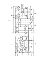
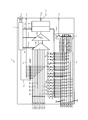
- FIG. 3 is a detailed configuration diagram of a preamplifier unit and a comparator unit according to the first embodiment.
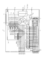
- FIG. 6 is another detailed configuration diagram of the preamplifier section and the comparator section of the first embodiment.
- It is a detailed block diagram corresponding to two pixel signals of the preamplifier unit of the first embodiment.
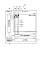
- FIG. 1 is a block diagram showing a configuration example of an electronic device according to an embodiment.
- the electronic device 100 roughly includes a solid-state image sensor 1, an image processing unit 8, and a control unit 9.
- the solid-state imaging device 1 includes a pixel array unit 2, a row scanning circuit 3, an A / D conversion unit 4, a timing control unit 5, a column scanning circuit 6, and a signal processing unit 7.
- the pixel array unit 2 is provided with a plurality of scanning lines and a plurality of signal lines, and pixel circuits are arranged at the intersections of the respective scanning lines and the respective signal lines to form a two-dimensional array.
- a plurality of pixel circuits are provided in a grid pattern.
- the row scanning circuit 3 sets any one of the plurality of scanning lines to the active state and configures the pixel array unit 2 corresponding to the scanning line in the active state.
- the pixel circuits for one row are driven to output pixel signals.
- the A / D conversion unit 4 has a plurality of A / D converters described later, performs A / D conversion of the voltage corresponding to the input pixel signal, and outputs pixel data to the signal processing unit 7. ..
- the timing control unit 5 controls the timing at which each of the row scanning circuit 3, the A / D conversion unit 4, and the column scanning circuit 6 operates under the control of the control unit 9.
- the column scanning circuit 6 operates under the control of the timing control unit 5 in synchronization with the operations of the row scanning circuit 3 and the A / D conversion unit 4, and the A / D conversion unit 4 performs A / D conversion for each signal line.
- the obtained data is sequentially transferred to the signal processing unit 7 as pixel data.
- the signal processing unit 7 performs processing such as automatic gain control and noise cancellation on image data composed of a plurality of pixel data, and outputs the image data to an external image processing unit 8.
- the image processing unit 8 executes various image processes on the image data under the control of the control unit 9. In this image processing, for example, demosaicing processing, white balance processing, etc. are executed. Then, the image data after the image processing is transmitted to an external recording device such as an image memory.
- the image processing unit 8 is arranged outside the solid-state imaging device 1, but it is also possible to provide the image processing unit 8 inside the solid-state imaging device 1.
- each of the circuits in the solid-state imaging device 1 may be arranged on a single semiconductor substrate or may be arranged dispersedly on a plurality of laminated semiconductor substrates.
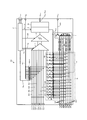
- FIG. 2 is a diagram illustrating a configuration example of the A / D converter according to the first embodiment.
- the A / D converter 10 is roughly classified into a local reference voltage generation unit 11, a DA conversion unit 12, a preamplifier unit 13, a comparator unit 14, a successive conversion logic unit 15, a column interface unit 16, as shown in FIG.
- a clock generation / logic control block 17 and preamplifier through switch groups SWG TM and SWTN are provided.
- the local reference voltage generation unit 11 generates and outputs a plurality of types of local reference reference signals (local reference reference voltages) VRT0, VRT1, VRT2, VRC, VRB2, VRB1, VRB0 from the reference voltage T GRV .
- VRT0 VRC + VREF / 2
- VRT1 VRC + VREF / 8
- VRT2 VRC + VREF / 32
- VRB2 VRC-VREF / 32
- VRB1 VRC-VREF / 8
- VRB0 VRC-VREF / 2
- the DA conversion unit 12 uses a plurality of types of local reference reference signals Sref generated by the local reference voltage generation unit 11, and under the control of a successive conversion logic unit 15 described later, digital / analog (D / A) of the control data D SAR. The conversion is performed and the threshold voltage signal Sth is output.
- the preamplifier unit 13 amplifies the differential voltage of the pixel signals SV 1 to SV 8 and the threshold voltage signal Sth input from the pixel array unit 2 through the coupling capacitors from the plurality of pixel signal input terminals TV 1 to TV 8 and outputs the amplified voltage.
- the amplification operation signal is output to the signal lines OUTP and OUTN.
- the comparator unit 14 compares the preamplifier output signals OUTP and OUTN and outputs the comparison result data D CMP .
- the sequential conversion logic unit 15 outputs the control data D SAR of the digital / analog conversion unit from the comparison result data D CMP under the control of the clock generation / logic control block 17.
- the sequential conversion logic unit 15 also stores the input comparison result data D CMP and outputs pixel data that is an analog / digital (A / D) conversion result of a pixel signal based on the stored comparison result data D CMP. ..
- the column interface unit 16 outputs pixel data D V1 to D V8 , which are analog / digital (A / D) conversion results of the pixel signals TV1 to TV8, from the output terminal TD OUT at a predetermined output timing.
- the clock generation / logic control block 17 supplies the comparison signal CLK to the comparator unit 14 and the enable signal S EN to the preamplifier unit 13.
- the clock generation / logic control block 17 also supplies control signals S TM and SEL1 to SEL8 for switching the preamplifier through mode.
- the enable signal S EN functions as a first control signal
- the through mode control signal S TM and the pixel selection signals SEL1 to SEL8 function as a second control signal.
- the preamplifier through switch group SWG TM uses the through mode control signal S TM and the pixel selection signals SEL1 to SEL8 to output the pixel signals SV1 to SV8 input from the signal input terminals TV1 to TV8 via the coupling capacitors.
- a plurality of switching elements SWT1 to SWT8 and SWS1 to SWS8 are provided for directly leading to the comparator section 14 without going through 13.
- the through mode control signal S TM is output to each of the plurality of switching elements SWT1 to SWT8 and SW TN .
- the corresponding selection signals SEL1 to SEL8 are input to be exclusively turned on (closed) and input.
- a plurality of switching elements SWS1 to SWS8 for sequentially guiding any of the pixel signals SV1 to SV8 to the comparator section 14 directly without passing through the preamplifier section 13 are provided.
- the pre-amplifier through the switch group SWG TM, a plurality of switching elements SWT1 ⁇ SWT8, SW TN and a plurality of switching elements SWS1 ⁇ SWS8 constitute a preamplifier through circuit.
- the plurality of switching elements SWT1 to SWT8 are illustrated at positions separated from the signal lines extending from the pixel signal input terminals SV1 to SV8 to the preamplifier unit 13, respectively.
- the wiring capacitance of the bypass wiring of the switching elements SWT1 to SWT8 it is provided near the signal line toward the preamplifier unit 13.
- the plurality of switching elements SWS1 to SWS8 are also shown in positions separated from the output signal line OUTP, but in reality, in order to reduce the influence of the wiring capacitance of the bypass wiring of the switching elements SWS1 to SWS8, the output signals It is arranged close to the line OUTP.
- both the switching elements SWT1 to SWT8 and SW TN and the switching elements SWS1 to SWS8 are provided as the preamplifier through switch group SWG TM , but any one of the switching elements SWT1 to SWT8 or the switching elements SWS1 to SWS8 is provided.
- the preamplifier unit 13 is operated in a preamplifier through mode described later, the same effect can be obtained by sequentially and exclusively turning on a plurality of switching elements provided (closed state). It is possible.
- one switching element SW TN is provided as a preamplifier through switch on the threshold voltage terminal side of the preamplifier section 13.
- two switching elements connected in series are provided, For the same reason as described above, the wiring capacitance can be further reduced.
- FIG. 3 is a detailed configuration diagram of an example of the preamplifier unit and the comparator unit according to the first embodiment.
- the preamplifier unit 13 is of the PMOS input type.
- the preamplifier unit 13 has a source terminal S connected to a power supply line AVD, a gate terminal G connected to a drain terminal D, and a diode-connected P-channel MOS transistor TR11, and a power supply line AVD connected to a source terminal S and a gate.
- the terminal G is connected to the gate terminal G of the P-channel MOS transistor TR11, the P-channel MOS transistor TR11 and the P-channel MOS transistor TR12 functioning as a current mirror circuit, and one end thereof is connected to the drain terminal D of the P-channel MOS transistor TR11.
- the other end of the constant current source CC is connected to the ground line AVS.
- the pixel signal SV X is input to the gate terminal G
- the source terminal is connected to the drain terminal of the P-channel MOS transistor TR12
- the source terminal S is the P-channel MOS transistor TR13.
- the P-channel MOS transistor TR14 which is connected to the drain terminal D of the P-channel MOS transistor TR14 and which receives the operating voltage BIAS at the gate terminal G and functions as a cascode circuit.
- a load resistor R1 connected to the line AVS.
- the threshold voltage signal Sth is input to the gate terminal G
- the source terminal S is connected to the drain terminal D of the P-channel MOS transistor TR12
- the source terminal S is the P-channel MOS transistor.
- a P-channel MOS transistor TR16 that is connected to the drain terminal D of the transistor TR15 and the operating voltage BIAS is input to the gate terminal G and functions as a cascode circuit. One end is connected to the drain terminal D of the P-channel MOS transistor TR16 and the other end is connected.
- a load resistor R2 connected to the ground line AVS.
- the preamplifier unit 13 also includes a P-channel MOS transistor TR17 for applying the initial voltage VSET to the P-channel MOS transistor TR15 and a P-channel MOS transistor TR18 for applying the initial voltage VSET to the P-channel MOS transistor TR13. I have it.
- the preamplifier unit 13 includes the following switching elements SW1 to SW10 for the preamplifier through mode.
- the preamplifier unit 13 includes a switching element SW1 for connecting the gate terminal G of the P-channel MOS transistor TR11 and the gate terminal G of the P-channel MOS transistor TR12 to the power supply line AVD in the preamplifier through mode, and the P-channel MOS.
- the preamplifier unit 13 connects the switching element SW4 for connecting the source terminals S of the P-channel MOS transistors TR13, TR15 to the ground line AVS and the drain terminal D of the P-channel MOS transistors TR13, TR15 to the ground line AVS.
- Switching elements SW5 and SW6 for connecting the source terminals S of the P-channel MOS transistors TR13, TR15 to the ground line AVS switches the switching element SW4 for connecting the source terminals S of the P-channel MOS transistors TR13, TR15 to the ground line AVS and the drain terminal D of the P-channel MOS transistors TR13, TR15 to the ground line AVS.
- Switching elements SW5 and SW6 for connecting the source terminals S of the P-channel MOS transistors TR13, TR15 to the ground line AVS.
- the preamplifier unit 13 connects the switching element SW7 for connecting the gate terminal G of the P-channel MOS transistor TR13 to one input terminal of the comparator unit 14 and the gate terminal G of the P-channel MOS transistor TR15 of the comparator unit 14.
- P-channel MOS transistor TR13, P-channel MOS transistor TR14, P-channel MOS transistor TR15, P-channel MOS transistor TR16, load resistor R1 and load resistor R2 form a differential amplifier DA.
- FIG. 4 is a detailed configuration diagram of another example of the preamplifier section and the comparator section of the first embodiment.
- FIG. 4 shows the case where the preamplifier unit 13 is of the NMOS input type.
- the source terminal S is connected to the ground line AVS
- the gate terminal G is diode-connected to the drain terminal D
- the source terminal S is connected to the ground line AVS.
- the N-channel MOS transistor TR11X is connected to the gate terminal G of the N-channel MOS transistor TR11X and functions as a current mirror circuit with the N-channel MOS transistor TR11X.
- One end is connected to the drain terminal D of the N-channel MOS transistor TR11X and the other end is connected.
- a constant current source CC connected to the power supply line AVD.
- the pixel signal SV X is input to the gate terminal G
- the source terminal S is connected to the drain terminal D of the N-channel MOS transistor TR12X
- the source terminal S is an N-channel MOS transistor.
- An N-channel MOS transistor TR14X which is connected to the drain terminal D of the transistor TR13X, receives the operating voltage BIAS at the gate terminal G thereof, and functions as a cascode circuit, and has one end connected to the drain terminal D of the N-channel MOS transistor TR14X and the other end.
- a load resistor RX1 connected to the power supply line AVD.
- the threshold voltage signal Sth is input to the gate terminal G
- the source terminal S is connected to the drain terminal D of the N-channel MOS transistor TR12X
- the source terminal S is an N-channel MOS transistor.
- An N-channel MOS transistor TR16X that is connected to the drain terminal D of the transistor TR15X and receives the operating voltage BIAS at the gate terminal G to function as a cascode circuit, and one end of the N-channel MOS transistor TR16X is connected to the drain terminal D of the N-channel MOS transistor TR16X and the other end. Is equipped with a load resistor RX2 connected to the power supply line AVD.
- the preamplifier unit 13 also includes a P-channel MOS transistor TR18X for applying the initial voltage VSET to the N-channel MOS transistor TR13X and a P-channel MOS transistor TR17X for applying the initial voltage VSET to the P-channel MOS transistor TR15X. I have it. Further, the preamplifier unit 13 includes the following switching elements SW11 to SW20 for the preamplifier through mode.
- the preamplifier unit 13 includes a switching element SW11 for connecting the gate terminal G of the N-channel MOS transistor TR11X and the gate terminal G of the N-channel MOS transistor TR12X to the ground line AVS in the preamplifier through mode, and the N-channel MOS.
- the switching element SW13 for disconnecting is provided.
- the preamplifier unit 13 includes a switching element SW14 for connecting the source terminal S of the N-channel MOS transistor TR13X and the source terminal S of the N-channel MOS transistor TR15X to the power supply line AVD in the preamplifier through mode, and the N-channel MOS transistor TR13X.
- the preamplifier section 13 connects the switching element SW17 for connecting the gate terminal G of the N-channel MOS transistor TR13X to one input terminal of the comparator section 14 and the gate terminal G of the N-channel MOS transistor TR15X of the comparator section 14.
- a switching element SW18 for connecting to the other input terminal, a switching element SW19 for disconnecting the drain terminal D of the N-channel MOS transistor TR14X and the load resistor RX1 in the preamplifier through mode, and a drain terminal D of the N-channel MOS transistor TR16X.
- a load resistor RX2 and a switching element SW20 for disconnecting the load resistor RX2 in the preamplifier through mode.
- the N-channel MOS transistor TR13X, the N-channel MOS transistor TR14X, the N-channel MOS transistor TR15X, the N-channel MOS transistor TR16X, the load resistor RX1 and the load resistor RX2 form a differential amplifier DAX.
- FIG. 5 is a detailed configuration diagram corresponding to two pixel signals of the preamplifier unit of the first embodiment.
- the preamplifier unit 13A is of the PMOS input type.
- the same parts as those of the preamplifier section 13 are designated by the same reference numerals.
- the preamplifier section 13A has a source terminal S connected to the power supply line AVD, a gate terminal G connected to a drain terminal D, and a diode-connected P-channel MOS transistor TR11, and a source terminal S connected to the power supply line AVD and a gate.
- the terminal G is connected to the gate terminal G of the P-channel MOS transistor TR11, and the P-channel MOS transistor TR12 functions as a current mirror circuit in cooperation with the P-channel MOS transistor TR11.
- One end of the P-channel MOS transistor TR11 has a drain terminal D.
- a constant current source CC having the other end connected to the ground line AVS.
- the pixel signal SV1 is input to the gate terminal G
- the source terminal S is connected to the drain terminal D of the P-channel MOS transistor TR12
- the pixel signal SV2 is input to the gate terminal G.
- a P-channel MOS transistor TR132 whose input is input and whose source terminal S is connected to the drain terminal D of the P-channel MOS transistor TR12, and whose source terminal S is the drain terminal D of the P-channel MOS transistor TR131 or the drain terminal D of the P-channel MOS transistor TR132.
- a bias current control signal BIAS is input to the gate terminal G of the P-channel MOS transistor TR14 that functions as a cascode circuit and one end of the P-channel MOS transistor TR14. The other end is connected to the down terminal D is provided with a load resistor R1 connected to the ground line AVS, the.
- the threshold voltage signal Sth is input to the gate terminal G
- the source terminal S is connected to the drain terminal D of the P-channel MOS transistor TR12
- the source terminal S is a P-channel MOS transistor.
- the drain terminal D of the transistor TR15 is connected
- the bias current control signal BIAS is input to the gate terminal G
- the P channel MOS transistor TR16 that functions as a cascode circuit and one end thereof are connected to the drain terminal D of the P channel MOS transistor TR16.
- a load resistor R2 having the other end connected to the ground line AVS.
- the preamplifier unit 13A includes a P-channel MOS transistor TR17 for applying the initial voltage VSET to the P-channel MOS transistor TR15, a P-channel MOS transistor TR181 for applying the initial voltage VSET to the P-channel MOS transistor TR131, and an N-type. P channel MOS transistor TR182 for applying initial voltage VSET to channel MOS transistor TR132.
- the preamplifier unit 13A includes the following switching elements SW1 to SW6, SW71, SW72, and SW8 to SW10 for the preamplifier through mode.
- the preamplifier unit 13A includes a switching element SW1 for connecting the gate terminal G of the P-channel MOS transistor TR11 and the gate terminal G of the P-channel MOS transistor TR12 to the power supply line AVD in the preamplifier through mode, and the P-channel MOS.
- a switching element SW2 for disconnecting the drain terminal D of the transistor TR11 and the constant current source CC in the preamplifier through mode, a drain terminal D of the P-channel MOS transistor TR12, and a source terminal S of the P-channel MOS transistors TR15, TR131, TR132.
- a switching element SW3 for disconnecting in the preamplifier through mode.
- the preamplifier unit 13A includes a switching element SW4 for connecting the source terminal S of the P-channel MOS transistors TR131 and TR132 and the source terminal S of the P-channel MOS transistor TR15 to the ground line AVS in the preamplifier through mode, and the P-channel MOS.
- SW6 is provided.
- the preamplifier unit 13A connects the switching elements SW71 and SW25 for connecting the gate terminal G of the P-channel MOS transistor TR131 to one input terminal of the comparator unit 14 and the gate terminal G of the P-channel MOS transistor TR132 with the comparator unit.
- Switching elements SW72 and SW26 for connecting to one input terminal of P14, switching element SW8 for connecting the gate terminal G of the P-channel MOS transistor TR15 to the other input terminal of the comparator section 14, and P-channel MOS transistor.
- a switching element SW9 for disconnecting the drain terminal D of the TR14 and the load resistor R1 in the preamplifier through mode, and a drain terminal D of the P-channel MOS transistor TR16 and the load resistor R2 are preamplified through.
- a switching element SW10 for disconnecting during over de.
- one of the connected P-channel MOS transistor TR131 or P-channel MOS transistor TR132, P-channel MOS transistor TR14, P-channel MOS transistor TR15, P-channel MOS transistor TR16, load resistor R1 and load resistor R2 is connected. Constitute a differential amplifier DA.
- the comparator unit 14 roughly includes an amplification unit (amplification stage) 14A and a latch unit 14B.
- the source terminal S is connected to the digital power supply DVD
- the gate terminal G is connected to the clock signal line CLK
- the drain terminal D is connected to the drain terminal D of the P-channel MOS transistor TR21.
- the N-channel MOS transistor TR22 having the gate terminal G connected to the positive input terminal INP, the source terminal S connected to the digital power supply DVD, and the gate terminal G connected to the clock signal line CLK are connected to the P-channel MOS transistor TR23.
- the drain terminal D is connected to the drain terminal D of the P-channel MOS transistor TR23, and the gate terminal G is connected to the negative side input terminal INN, and the drain terminal D is the N-channel MOS transistor TR2.
- Source terminal S and the source terminal S of the N channel MOS transistor TR24 are commonly connected, the gate terminal G is connected to the clock signal line CLK, and the source terminal S is connected to the digital ground DVS. I have it.
- the amplifier 14A includes a P-channel MOS transistor TR31 and an N-channel MOS transistor TR32 which form a CMOS inverter, and a P-channel MOS transistor TR33 and an N-channel MOS transistor TR34 which form a CMOS inverter.
- the signal is amplified by working together.
- the latch unit 14B has a source terminal S connected to the digital power supply DVD, a gate terminal G connected to the clock signal line CLK, a P-channel MOS transistor TR41, a source terminal S connected to the digital power supply DVD, and a drain terminal D.
- the P-channel MOS transistor TR42 connected to the drain terminal D of the P-channel MOS transistor TR41, the drain terminal D connected to the drain terminal D of the P-channel MOS transistor TR41 and the drain terminal D of the P-channel MOS transistor TR42, and the gate terminal G Is an N-channel MOS transistor TR43 connected to the source terminal S of the P-channel MOS transistor TR31 and the drain terminal D of the N-channel MOS transistor TR32, and the drain terminal D is an N-channel MOS transistor. Is connected to the source terminal S of the register TR43, the source terminal S is connected to the digital ground DVS, the gate terminal G is provided with an N-channel MOS transistor TR44 connected to the gate terminal G of the P-channel MOS transistor TR42, a.
- the latch section 14B has a source terminal S connected to the digital power supply DVD, a gate terminal G connected to the clock signal line CLK, a P-channel MOS transistor TR45, a source terminal S connected to the digital power supply DVD, and a drain terminal.
- D is connected to the drain terminal D of the P-channel MOS transistor TR45, and the gate terminal G is connected to the drain terminal D of the P-channel MOS transistor TR42 and the drain terminal D of the N-channel MOS transistor TR43.
- the terminal D is connected to the drain terminal D of the P-channel MOS transistor TR45 and the drain terminal D of the P-channel MOS transistor TR46, and the gate terminal G of the P-channel MOS transistor T constitutes an inverter.
- N-channel MOS transistor TR48 having a gate terminal G connected to the gate terminal G of the P-channel MOS transistor TR46.
- the A / D converter 10 sets the value (“1” or “0”) of all bits by performing successive comparison from the most significant bit to the least significant bit of the pixel data that is the A / D conversion result. There is. First, the successive conversion logic unit 15 sets all voltages to the center voltage (VRC) as an initial value.
- VRC center voltage
- the comparator unit 14 compares the voltages of the differential signals OUTP and OUTN and outputs the comparison result data D CMPX to the successive conversion logic unit 15.
- Sequential conversion logic unit 15 the comparison result to generate the control data D SAR of the DA converter 12 in response to the result of the data D CMP, stores the comparison result data D CMP.
- the DA conversion unit 12 uses the plurality of types of local reference voltages VRT0 to VRT2, VRC, VRB0 to VRB2 generated by the local reference voltage generation unit 11 to perform digital / analog (D / A) conversion of the input control data D SAR. Then, the threshold voltage signal S th is output to the preamplifier unit 13.
- the most significant bit (MSB) to the least significant bit (LSB) are similarly sequentially compared, and the successive conversion logic unit 15 determines and stores the value of each bit. Then, when the values of all bits are determined, the stored data is output from the output terminal TD OUT as A / D conversion result data D V1 to D V8 .
- one of the switching elements SWT1 to SWT8 and the switching elements SWS1 to SWS8 is turned on (closed) so that the pixel signals SV1 to SV8 input from the pixel signal input terminals TV1 to TV8 are input.
- a signal path that can bypass the preamplifier unit 13 is formed.
- the switching element SW TN is turned on (closed) to form a signal path that can bypass the preamplifier unit 13.
- the preamplifier 13 When bypass the preamplifier 13 by blocking the preamplifier section 13 electrically, only the signal path through the signal path as well as the switching element SW TN via the switching elements SWT1 ⁇ SWT8 and switching elements SWS1 ⁇ SWS8 becomes effective,
- the pixel signals SV 1 to SV 8 and the threshold voltage S th input from the pixel signal input terminals TV 1 to TV 8 are bypassed to the comparator unit 14 as they are without passing through the preamplifier unit 13.
- the bypass path is set to the on state (closed state) only in the portion that executes the A / D conversion.
- the switching element SW1 is turned on (closed), and the gate terminal G of the P-channel MOS transistor TR11 and the gate terminal of the P-channel MOS transistor TR12 are connected to the power supply line AVD.
- the switching element SW2 is turned off (open state), the drain terminal D of the P-channel MOS transistor TR11 and the constant current source CC are separated, and the switching element SW3 is turned off (open state) to set the P-channel.
- the drain terminal D of the MOS transistor TR12 and the source terminal S of the P-channel MOS transistor TR15 are separated.
- the current source that supplies power to the preamplifier unit 13 is cut off so that a steady current does not flow.
- the switching elements SW4, SW5 and SW6 are turned on (closed state), and the source terminal S and drain terminal D of the P-channel MOS transistor TR13 and the source terminal S and drain terminal D of the P-channel MOS transistor TR15 are connected to the ground line AVS.
- the ground line AVS functions as a ground
- the drain terminals D and the source terminals S of the P-channel MOS transistor TR13 and the P-channel MOS transistor 15 functioning as input transistors are commonly connected to the ground.
- the P-channel MOS transistor TR13 and the P-channel MOS transistor 15 are turned off regardless of the voltage.
- the gate terminals G of the P-channel MOS transistor TR14 and the P-channel MOS transistor TR16 are respectively set to the power supply line AVD, so that both the P-channel MOS transistor TR14 and the P-channel MOS transistor TR16 are turned off.
- the switching element SW9 is turned off (open state), the drain terminal D of the P-channel MOS transistor TR14 is disconnected from the load resistor R1, the switching element SW10 is turned off (open state), and the drain of the P-channel MOS transistor TR16.
- the terminal D and the load resistor R2 are separated to bring the output of the preamplifier unit 13 into a high impedance state.
- the switching element SW7 is turned on (closed state)
- the gate terminal G of the P-channel MOS transistor TR13 is connected to one input terminal of the comparator section 14, and the switching element SW8 is turned on (closed) to set the P-channel.
- the gate terminal G of the MOS transistor TR15 is connected to the other input terminal of the comparator section 14 to bring the input / output of the preamplifier section 13 into the through state.
- the comparator unit 14 is in a state in which it can operate independently. That is, in the above configuration, the preamplifier unit 13 is powered down, the pixel signal SVX and the threshold voltage S th are bypassed in the preamplifier unit 13, and directly input to the comparator unit 14.
- the electronic device 100 of the first embodiment when the quantization error and the streaking characteristic are not severe and the number of pixels is low, the input / output of the preamplifier unit 13 is passed through and the power of the preamplifier unit 13 is reduced. By performing the down, it is possible to reduce power consumption.
- the difference between the A / D converter 10A of the second embodiment and the A / D converter 10 of the first embodiment is that the operation period of the preamplifier unit 13 is shortened without passing through the preamplifier unit 13 to reduce power consumption. Is the point that has been realized. Specifically, since the number of A / D bits is small when the number of pixels is low (in the low bit mode), the number of conversions of the converter can be reduced in the successive approximation conversion method, which is effective when compared with the case of high pixels. The operating time can be shortened.
- FIG. 6 is a diagram illustrating a configuration example of the A / D converter according to the second embodiment.
- the same parts as those of the A / D converter 10 of the first embodiment of FIG. 2 are denoted by the same reference numerals, and the detailed description thereof is incorporated.
- the A / D converter 10A is roughly classified into a local reference voltage generation unit 11, a DA conversion unit 12, a preamplifier unit 13, a comparator unit 14, a successive conversion logic unit 15, a column interface unit 16, as shown in FIG.
- a clock generation / logic control block 17 and a reset switch group SWG RT are provided.
- the "period" is different between the high bit mode and the low pixel mode, and the enable period is shortened in the low pixel mode.
- the number of CLKs to the comparator unit 14 is reduced.
- the control logic D SAR from the successive conversion logic unit 15 to the DA conversion unit 12 is also reduced by the reduction in the number of comparisons.
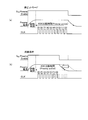
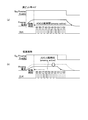
- FIG. 7 is an operation explanatory diagram of the second embodiment.
- the second embodiment there are two operation modes, a high bit mode and a low pixel mode, which will be sequentially described.
- the number of comparisons of the comparator unit 14 is 10 in the high bit mode and that of the comparator unit 14 is 7 in the low pixel mode.
- FIG. 7A is an operation timing chart in the high bit mode. First, the operation in the high bit mode will be described.
- the activation time of the preamplifier + the comparison time of 10 times of the comparator unit 14 is the conversion time of one pixel signal.
- FIG. 7B is an operation timing chart in the low pixel mode.
- the operation period of the preamplifier unit 13 can be reduced, and the power consumption of the preamplifier unit 13 can be reduced.
- n is 2 or more in the pixel addition mode without passing through the preamplifier unit 13.
- a pixel addition switch for adding pixel signals of (natural number) is provided, and the processing time is effectively reduced to 1 / n by processing the n pixels as one pixel.
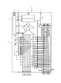
- FIG. 8 is a diagram illustrating a configuration example of the A / D converter according to the third embodiment.
- the same parts as those of the A / D converter 10 of the first embodiment of FIG. 2 are designated by the same reference numerals, and the detailed description thereof is incorporated.
- the A / D converter 10B is roughly classified into a local reference voltage generation unit 11, a DA conversion unit 12, a preamplifier unit 13, a comparator unit 14, a successive conversion logic unit 15, a column interface unit 16, as shown in FIG.
- the clock generation / logic control block 17, the pixel addition switches SWP1 to SWP4, and the reset switch group SWG RT are provided.
- the pixel addition switch SWP1 when the pixel addition switch SWP1 is turned on, the added voltage of the voltage of the pixel signal SV1 and the voltage of the pixel signal SV2 is applied to the input terminal of the pixel signal SV1 of the preamplifier unit 13.
- the pixel addition switch SWP2 when the pixel addition switch SWP2 is turned on, the added voltage of the voltage of the pixel signal SV3 and the voltage of the pixel signal SV4 is applied to the input of the pixel signal SV3 of the preamplifier unit 13.
- the pixel addition switch SWP3 when the pixel addition switch SWP3 is turned on, the added voltage of the voltage of the pixel signal SV5 and the voltage of the pixel signal SV6 is applied to the input terminal of the pixel signal SV5 of the preamplifier unit 13.
- the pixel addition switch SWP4 When the pixel addition switch SWP4 is turned on, the addition voltage of the voltage of the pixel signal SV7 and the voltage of the pixel signal SV8 is applied to the input of the pixel signal SV7 of the preamplifier unit 13.
- FIG. 9 is an operation explanatory diagram of the third embodiment. Also in FIG. 9, the horizontal axis is the time axis.
- the normal mode there are two operation modes, that is, the normal mode and the pixel addition mode, and they will be sequentially described.
- the normal mode A / D conversion processing of pixel signals is performed in pixel units
- the pixel addition mode A / D conversion of pixel signals is performed in units of a plurality of pixels (two pixels in the third embodiment). D conversion processing is being performed.
- FIG. 9A shows a timing chart of the preamplifier enable signal SEN in the normal mode
- FIG. 9C shows a timing chart of the clock signal CLK of the A / D conversion processing of the third embodiment. Shows.
- the preamplifier unit 13 is activated in each of the eight AD periods from ADC1 to ADC7.
- FIGS. 9A and 9B are operation timing charts in the pixel addition mode.
- all the pixel addition switches SWP1 to SWP4 are turned on.
- the added voltage of the voltage of the pixel signal SV1 and the voltage of the pixel signal SV2 is applied to the input terminal of the pixel signal SV1 of the preamplifier section 13, and the pixel signal SV3 is input to the input terminal of the preamplifier section 13.
- the added voltage of the voltage of SV3 and the voltage of the pixel signal SV4 is applied, and the added voltage of the voltage of the pixel signal SV5 and the voltage of the pixel signal SV6 is applied to the input terminal of the pixel signal SV5 of the preamplifier unit 13, and the preamplifier unit
- the addition voltage of the voltage of the pixel signal SV7 and the voltage of the pixel signal SV8 is applied to the input terminal of the pixel signal SV7 of No. 13.
- the number of AD conversions is half that in the normal mode, so the number of times the preamplifier unit 13 is activated is half that in the normal mode, and the preamplifier unit 13 operates only for about half the time. Therefore, the power consumption of the preamplifier unit 13 can be halved (reduced). Similarly, it becomes possible to reduce (reduce) the power of the successive conversion block by half.
- the four pixel data DV1, DV3, DV5, and DV7 corresponding to the corresponding four addition voltages are output, and the processing time and power consumption are about half of those in the normal mode. It becomes possible. That is, according to the third embodiment, by grouping a plurality of pixels and performing processing by regarding n pixels as one pixel, the processing time is effectively reduced to 1 / n and the power consumption is approximately The power consumption of the solid-state image sensor 1 can be reduced to 1 / n.
- the A / D converter 10C of the fourth embodiment is different from the A / D converter 10 of the first embodiment in that it does not pass through the preamplifier section 13 and in the low pixel mode (low bit mode). In order to reduce the power consumption, the linearity and noise characteristics of the preamplifier are relaxed because the value of 1LSB increases and the quantization error increases.
- FIG. 10 is a diagram illustrating a configuration example of the A / D converter according to the fourth embodiment.
- the A / D converter 10C is roughly classified into a local reference voltage generation unit 11, a DA conversion unit 12, a preamplifier unit 13A, a comparator unit 14, a successive conversion logic unit 15, a column interface unit 16, as shown in FIG.
- a clock generation / logic control block 17 and a reset switch group SWG RT are provided.
- the configuration of the A / D converter 10C is different from that of the A / D converter 10 of the first embodiment in FIG. 2 in that the preamplifier through switch group SWG TM is not provided and the preamplifier current supplied to the preamplifier unit 13A. Since it is possible to reduce (for example, halve), the description of the other parts will be incorporated.
- FIG. 11 is an operation explanatory diagram of the fourth embodiment. Also in the fourth embodiment, there are two operation modes, a high bit mode and a low pixel mode, which will be sequentially described.
- FIG. 11A is an operation timing chart in the high bit mode. First, the operation in the high bit mode will be described.
- FIG. 11B is an operation timing chart in the low pixel mode.
- the value of 1LSB increases and the quantization error increases, so that the linearity and noise characteristics required for the preamplifier are alleviated. Therefore, the current of the preamplifier unit 13 can be reduced as compared with the high bit mode.
- the difference from the high bit mode is that the current at the time of starting the preamplifier is smaller than that in the high bit mode. This makes it possible to reduce power consumption.
- the value of 1LSB increases and the quantization error increases, so that the linearity and noise characteristics required for the preamplifier unit 13 are alleviated.
- the preamplifier current flowing through the preamplifier unit 13 it is possible to reduce the power consumption of the preamplifier unit 13 and thus reduce the power consumption of the electronic device 100.
- FIG. 12 is a diagram illustrating a configuration example of the A / D converter of the fifth embodiment. 12 is different from the first embodiment shown in FIG. 2 in that the pixel addition switches SWP1 to SWP4 are provided. That is, the fifth embodiment is an embodiment in which the first embodiment and the third embodiment are combined.
- switching elements SWT1, SWS1, SWT2, and SWS2 are provided for preamplifier through of the pixel signals SV1 and SV2.
- a switching element SWP1 is provided for pixel addition of the pixel signal SV1 and the pixel signal SV2.
- switching elements SWT3, SWS3 and SWT4 and SWS4 are provided for preamplifier through of the pixel signals SV3 and SV4.
- a switching element SWP2 is provided for pixel addition of the pixel signal SV3 and the pixel signal SV4.
- switching elements SWT5, SWS5 and SWT6 and SWS6 are provided for preamplifier through of the pixel signals SV5 and SV6.
- a switching element SWP3 is provided for pixel addition of the pixel signal SV5 and the pixel signal SV6.
- switching elements SWT7, SWS7 and SWT8 and SWS8 are provided for preamplifier through of the pixel signals SV7 and SV8.
- a switching element SWP4 is provided for pixel addition of the pixel signal SV7 and the pixel signal SV8.
- the preamplifier unit 13 shifts to a power down mode in which the image pickup device 1 and thus the electronic device are stopped.
- the power consumption of the entire 100 can be reduced.
- four pixel data DV1, DV3, DV5, DV7 corresponding to the pixel signals corresponding to the corresponding four addition voltages are output, and the processing time is halved to reduce the power consumption in the normal mode. It can be reduced to about half.
- a plurality of pixels are grouped and n pixels are regarded as one pixel to perform processing, thereby effectively reducing the processing time to 1 / n and the power consumption.
- the power consumption of the solid-state image sensor 1 can be further reduced.
- FIG. 13 is a block diagram of an example of an indirect light time-of-flight distance sensor to which the present technology is applied.
- An indirect-time of flight type distance sensor 100 includes a sensor chip 101 and a circuit chip 102 stacked on the sensor chip 101.
- the pixel array section 112 has a plurality of pixels 111 arranged in an array on the sensor chip 101 in a two-dimensional grid pattern.
- the pixel array unit 112 may be arranged in a matrix and may include a plurality of column signal lines. Each column signal line is connected to each pixel.
- a vertical drive circuit 113, a column signal processing unit 114, a timing adjustment circuit 115, and an output circuit 116 are arranged on the circuit chip 102.
- the vertical drive circuit 113 is configured to drive pixels and output pixel signals to the column signal processing unit 114.
- the column signal processing unit 114 performs A / D conversion processing on the input pixel signal and outputs the pixel data subjected to the A / D conversion processing to the output circuit 116.
- the output circuit 116 performs a CDS (Correlated Double Sampling) process or the like on the pixel data from the column signal processing unit 114, and outputs the pixel data to the signal processing circuit at the subsequent stage.
- CDS Correlated Double Sampling
- the timing control circuit 115 is configured to control the drive timing of each vertical drive circuit 113.
- the column signal processing unit 114 and the output circuit 116 operate in synchronization with the vertical synchronization signal output from the timing control circuit 115.
- FIG. 14 is a circuit diagram showing a configuration example of a pixel according to the embodiment of the present technology.
- the pixel 111 includes a photodiode 121, two transfer transistors 122 and 123, two reset transistors 124 and 125, two taps (floating diffusion layers 126 and 127), two amplification transistors 128 and 129, and two selection transistors 130, 131 is provided.
- the photodiode 121 photoelectrically converts the received light to generate an electric charge.
- the photodiode 121 is arranged on the back surface with respect to the front surface with the surface on the semiconductor substrate on which the circuit is arranged as the front surface.
- Such a solid-state image sensor is called a backside illumination type solid-state image sensor.
- a frontside illumination type configuration in which the photodiode 121 is arranged on the front side can be used.
- the transfer transistor 122 and the transfer transistor 123 sequentially transfer charges from the photodiode 121 to the TAPA 126 and TAPB 127 in accordance with the transfer signal TRG from the vertical drive circuit 113.
- the TAPA 126 and the TAPB 127 accumulate the transferred charges and generate a voltage according to the amount of the accumulated charges.
- the overflow transistor 132 is a transistor that sequentially discharges the charges of the photodiode 121 to the high-potential side power supply VDD, and has a function of resetting the photodiode 121.
- the reset transistors 124 and 125 extract the charges from the respective TAPA 126 and TAPB 127 in accordance with the reset signal RSTp from the vertical drive circuit 113 to initialize the amount of charges.
- the amplification transistors 128 and 129 amplify the voltages of the TAPA 126 and TAPB 127, respectively.
- the selection transistors 130 and 131 output the signal of the amplified voltage as a pixel signal to the column signal processing unit 114 via two vertical signal lines (for example, VSL1 and VSL2). To do.
- the vertical signal line and the vertical signal line VSL2 are connected to the input of one A / D converter 10 in the column signal processing unit 114.
- the circuit configuration of the pixel 111 is not limited to the configuration illustrated in FIG. 15 as long as the pixel signal can be generated by photoelectric conversion.
- a pixel array section in which a plurality of pixels that perform photoelectric conversion and output pixel signals are arranged in an array;
- the pixel signal and the threshold signal are input to an input terminal, the pixel signal and the threshold signal are amplified and output from the output terminal as a first signal and a second signal, and based on the input first control signal.
- a preamplifier section that is in an operation stopped state, A comparator unit that receives the first signal and the second signal from the first input terminal and the second input terminal, compares the first signal and the second signal, and outputs comparison result data; A preamplifier through circuit that has a plurality of switching elements that connect the input terminals of the preamplifier section to the input terminals of the comparator section, and sets the switching elements to the connection state based on the second control signal that is input in the operation stop state.
- a solid-state image sensor including.
- the preamplifier through circuit is provided with a pair of switching elements on a signal line for connecting an input terminal of the preamplifier section to a corresponding input terminal of the comparator section, One of the pair of switching elements is arranged near the input terminal of the preamplifier section, and the other is arranged near the input terminal of the comparator section.
- the preamplifier section electrically disconnects the preamplifier section from the pixel array section and the comparator section when the pixel signal and the threshold signal are output to the comparator section via the preamplifier through circuit.
- a plurality of second switching elements for shifting to the operation stop state are provided, The solid-state image sensor according to (1) or (2).
- the second switching element electrically disconnects the preamplifier unit in a high impedance state, (3) The solid-state image sensor according to the above.
- a sequential conversion block unit that determines pixel data that is an A / D conversion result of the pixel signal based on the comparison result data, The solid-state image sensor according to any one of (1) to (4).
- the first control signal is input when operating the solid-state imaging device in a low pixel mode, The solid-state image sensor according to any one of (1) to (5).
- a plurality of pixel addition switching elements that connect the plurality of first input terminals to each other every n pieces and that use the potentials of the n pieces of the first input terminals connected to each other as addition potentials;
- the solid-state image sensor according to any one of (1) to (6).
- a pixel array section in which a plurality of pixels that perform photoelectric conversion and output pixel signals are arranged in an array; The pixel signals are input to the corresponding input terminals, the threshold signal is input to the corresponding input terminals, the pixel signals and the threshold signals are amplified, and the plurality of first signals and the second signals are output from the corresponding output terminals.
- a preamplifier section that outputs as a signal
- a comparator unit that inputs the first signal from a first input terminal and inputs the second signal from a second input terminal, compares the first signal and the second signal, and outputs comparison result data
- a plurality of pixel addition switching elements in which the plurality of first input terminals are connected to each other every n pieces, and the electric potentials of the n pieces of the first input terminals connected to each other are set as addition potentials;
- a solid-state image sensor including.
- a pixel array section in which a plurality of pixels that perform photoelectric conversion and output pixel signals are arranged in an array;
- the pixel signal is input to each of a plurality of corresponding input terminals, a threshold signal is input to the corresponding input terminal, the pixel signal and the threshold signal are amplified, and a first signal and a second signal are output from the corresponding output terminals.
- Output preamp section A comparator unit that inputs the first signal from a first input terminal, inputs the second signal from a second input terminal, compares the first signal and the second signal, and outputs comparison result data; Prepare, Based on the input control signal, in a case where the preamplifier section has a use condition in which the linearity and noise characteristics can be relaxed, the preamplifier current flowing through the preamplifier section is reduced.
- Solid-state image sensor Solid-state image sensor.
- a pixel array section in which a plurality of pixels that perform photoelectric conversion and output pixel signals are arranged in an array;
- the pixel signal is input to each of a plurality of corresponding input terminals, a threshold signal is input to the corresponding input terminal, the pixel signal and the threshold signal are amplified, and a first signal and a second signal are output from the corresponding output terminals.
- Output preamp section A comparator unit that inputs the first signal from a first input terminal, inputs the second signal from a second input terminal, compares the first signal and the second signal, and outputs comparison result data; A sequential conversion block unit that determines pixel data that is an A / D conversion result of the pixel signal based on the comparison result data, The comparator section performs the comparison based on the input control signal, and when the accuracy of the pixel data is not required, the number of comparisons is reduced based on the control signal.
- Solid-state image sensor Solid-state image sensor.
- a solid-state image sensor for outputting a plurality of pixel data, An image processing unit that performs image processing on image data corresponding to the plurality of pixel data; A control unit that controls the solid-state imaging device and the image processing unit, The solid-state image sensor, A pixel array section in which a plurality of pixels that perform photoelectric conversion and output pixel signals are arranged in an array; The pixel signal and the threshold signal are input to an input terminal, the pixel signal and the threshold signal are amplified and output from the output terminal as a first signal and a second signal, and based on the input first control signal.
- a preamplifier section that is in an operation stopped state, A comparator unit that inputs the first signal from a first input terminal and inputs the second signal from a second input terminal, compares the first signal and the second signal, and outputs comparison result data; A preamplifier through circuit that has a plurality of switching elements that connect the input terminals of the preamplifier section to the input terminals of the comparator section, and sets the switching elements to the connection state based on the second control signal that is input in the operation stop state.
- a solid-state image sensor for outputting a plurality of pixel data, An image processing unit that performs image processing on image data corresponding to the plurality of pixel data; A control unit that controls the solid-state imaging device and the image processing unit, The solid-state image sensor, A pixel array section in which a plurality of pixels that perform photoelectric conversion and output pixel signals are arranged in an array; A preamplifier unit that inputs the pixel signal to each of a plurality of input terminals, inputs a threshold signal to an input terminal, amplifies the pixel signal and the threshold signal, and outputs the amplified signal as a first signal and a second signal from corresponding output terminals.
- a comparator unit that inputs the first signal from a first input terminal and inputs the second signal from a second input terminal, compares the first signal and the second signal, and outputs comparison result data;
- a plurality of pixel addition switching elements in which the plurality of first input terminals are connected to each other every n pieces, and the electric potentials of the n pieces of the first input terminals connected to each other are set as addition potentials;
- a solid-state image sensor for outputting a plurality of pixel data, An image processing unit that performs image processing on image data corresponding to the plurality of pixel data; A control unit that controls the solid-state imaging device and the image processing unit, The solid-state image sensor, A pixel array section in which a plurality of pixels that perform photoelectric conversion and output pixel signals are arranged in an array; A preamplifier unit that inputs the pixel signal to each of a plurality of input terminals, inputs a threshold signal to an input terminal, amplifies the pixel signal and the threshold signal, and outputs the amplified signal as a first signal and a second signal from corresponding output terminals.
- a comparator unit that inputs the first signal from a first input terminal and inputs the second signal from a second input terminal, compares the first signal and the second signal, and outputs comparison result data; Equipped with Based on the input control signal, in a case where the preamplifier section has a use condition in which the linearity and noise characteristics can be relaxed, the preamplifier current flowing through the preamplifier section is reduced.
- the solid-state imaging device includes a preamplifier through circuit having a plurality of switching elements that connect an input terminal of the preamplifier section to a corresponding input terminal of the comparator section based on an input control signal. (13) The electronic device as described above.
- a solid-state image sensor for outputting a plurality of pixel data, An image processing unit that performs image processing on image data corresponding to the plurality of pixel data; A control unit that controls the solid-state imaging device and the image processing unit, The solid-state image sensor, A pixel array section in which a plurality of pixels that perform photoelectric conversion and output pixel signals are arranged in an array; The pixel signal is input to each of a plurality of corresponding input terminals, a threshold signal is input to the corresponding input terminal, the pixel signal and the threshold signal are amplified, and a first signal and a second signal are output from the corresponding output terminals.
- Output preamp section A comparator unit that inputs the first signal from a first input terminal and inputs the second signal from a second input terminal, compares the first signal and the second signal, and outputs comparison result data; Equipped with Based on the input control signal, in a case where the preamplifier section has a use condition in which the linearity and noise characteristics can be relaxed, the preamplifier current flowing through the preamplifier section is reduced.
- the pixel signal and the threshold signal are input to the input terminal, the pixel signal and the threshold signal are amplified and output from the output terminal as the first signal and the second signal, respectively, and based on the input first control signal.
- the preamplifier part that is stopped by A comparator unit that inputs the first signal from a first input terminal and inputs the second signal from a second input terminal, compares the first signal and the second signal, and outputs comparison result data; A preamplifier through circuit that has a plurality of switching elements that connect the input terminals of the preamplifier section to the input terminals of the comparator section, and sets the switching elements to the connection state based on the second control signal that is input in the operation stop state.
- a successive conversion block unit that determines A / D conversion result data of the first input signal based on the comparison result data; A / D converter provided with.
- the preamplifier through circuit is provided with a pair of switching elements on a signal line for connecting an input terminal of the preamplifier section to a corresponding input terminal of the comparator section, One of the pair of switching elements is arranged in proximity to the input terminal of the preamplifier section, and the other is arranged in proximity to the corresponding input terminal of the comparator section.
- the A / D converter described in. (18) The preamplifier section electrically disconnects the preamplifier section from the pixel array section and the comparator section when the pixel signal and the threshold signal are output to the comparator section via the preamplifier through circuit.
- a plurality of second switching elements for shifting to the operation stop state are provided, The A / D converter according to (16) or (17). (19) The second switching element electrically disconnects the preamplifier unit in a high impedance state, The A / D converter according to any one of (16) to (18).
- control unit 10 A / D converter 11 local reference voltage generation unit 12 DA conversion unit 13, 13A preamplifier unit 14 comparator unit 15 successive conversion logic unit DA differential amplifier SV1 to SV8 pixel signal S EV discrimination result signal SEL1 to SEL8 pixel selection signal (second control signal) S EN enable signal (first control signal) STM through mode control signal (second control signal) SW1 to SW10 Switching element (second switching element) SWT1 to SWT8 switching elements
Landscapes
- Engineering & Computer Science (AREA)
- Multimedia (AREA)
- Signal Processing (AREA)
- Theoretical Computer Science (AREA)
- Transforming Light Signals Into Electric Signals (AREA)
- Analogue/Digital Conversion (AREA)
- Control Of Motors That Do Not Use Commutators (AREA)
- Solid State Image Pick-Up Elements (AREA)
Abstract
本開示の固体撮像素子は、光電変換を行い画素信号をそれぞれ出力する複数の画素がアレイ状に配置された画素アレイ部(2)と、入力端子に画素信号及び閾値信号がそれぞれ入力され、画素信号と閾値信号との差を増幅して差動信号として出力するとともに、入力された第1制御信号(SEN)に基づいて動作停止状態とされるプリアンプ部(13)と、差動信号と比較基準信号との比較を行い比較結果データを出力するコンパレータ部(14)と、プリアンプ部(13)の入力端子をコンパレータ部(14)の入力端子に接続する複数のスイッチング素子を有し、動作停止状態において入力される第2制御信号(STM、SEL1~SEL8)に基づいてスイッチング素子を接続状態とするプリアンプスルー回路(SWGTM、SWT1~SWT8、SWTN、SWS1~SWS8)と、を備えるので、プリアンプ部に要求される特性が緩和できる条件では消費電力を抑制できる。
Description
本開示は、固体撮像素子及び電子機器に関する。
近年、半導体微細加工技術を応用したCMOS(Complementary Metal Oxide Semiconductor)イメージセンサ等の固体撮像素子がディジタルカメラやスマートフォン等において広く採用されている。
これらの固体撮像素子においては、各画素内に設けられた光電変換素子としてのフォトダイオードにおいて、被写体から入射した光が光電変換され、得られた電荷の量に対応する電圧信号が増幅トランジスタ及び垂直信号線を介して読み出されてコンパレータを有するA/D変換器によりアナログ/ディジタル(A/D)変換されて撮像データとして出力される。
ところで、CMOS等の撮像素子を用いた撮像装置において、逐次変換型のA/D変換を行う場合に、逐次変換型のA/D変換回路に用いられるコンパレータには、電力効率の良いダイナミックコンパレータが用いられるのが一般的である。
しかしながら、ダイナミックコンパレータは、キックバックノイズ量が大きく、撮像素子のように多数のA/D変換回路を用いて同時に動作させる場合には、電源、グランド、リファレンスなどの共通インピーダンスによりストリーキングが発生する虞があった。
ストリーキングを抑制するための技術としては、例えば、特許文献1記載の技術が提案されている。
ストリーキングを抑制するための技術としては、例えば、特許文献1記載の技術が提案されている。
ところで、ダイナミックコンパレータの前段にプリアンプを設け、高分解能を実現しようとする場合には、プリアンプに要求されるリニアリティやノイズ特性は、高い水準となり、これを実現するためのプリアンプは、消費電力が大きなものとなる。
本開示は、このような状況に鑑みてなされたものであり、ダイナミックコンパレータの前段に設けられるプリアンプが不要な場合には、プリアンプの入出力をショート、パワーダウンを行い、ダイナミックコンパレータで直接比較を行うことで、消費電力の低減を図ることが可能な固体撮像素子及び電子機器を提供することを目的としている。
本開示は、このような状況に鑑みてなされたものであり、ダイナミックコンパレータの前段に設けられるプリアンプのリニアリティやノイズ特性および間欠率を使用用途に応じて変更することで、消費電力の低減を図ることが可能な固体撮像素子及び電子機器を提供することを目的としている。
上記目的を達成するために、本開示の固体撮像素子は、光電変換を行い画素信号をそれぞれ出力する複数の画素がアレイ状に配置された画素アレイ部と、入力端子に画素信号及び閾値信号がそれぞれ入力され、画素信号と閾値信号との差を増幅して差動信号として出力するとともに、入力された第1制御信号に基づいて動作停止状態とされるプリアンプ部と、差動信号の比較を行い比較結果データを出力するコンパレータ部と、プリアンプ部の入力端子をコンパレータ部の入力端子に接続する複数のスイッチング素子を有し、動作停止状態において入力される第2制御信号に基づいてスイッチング素子を接続状態とするプリアンプスルー回路と、を備える。
本開示によれば、プリアンプ部は、入力された第1制御信号に基づいて動作停止状態とされ、このとき、プリアンプスルー回路は、動作停止状態において入力される第2制御信号に基づいてスイッチング素子を接続状態とするので、プリアンプ部を用いずにコンパレータ部を動作させることができ、消費電力を抑制できる。
本開示によれば、プリアンプ部に要求されるリニアリティやノイズなどの特性が緩和出来る条件では、プリアンプ部の電流を削減することで消費電力を抑制することができる。また、A/D変換に必要なビット数が少ない条件では変換回数を削減することが出来るため、間欠率を上げることで消費電力を抑制することが出来る。なお、ここに記載された効果は必ずしも限定されるものではなく、本開示中に記載されたいずれかの効果であってもよい。
以下に、本開示の実施形態について図面に基づいて詳細に説明する。なお、以下の各実施形態において、同様の部位には同一の符号を付することにより重複する説明を省略する。
(1)第1実施形態
[電子機器の構成例]
図1は、実施形態における電子機器の一構成例を示すブロック図である。
電子機器100は、大別すると、固体撮像素子1、画像処理部8及び制御部9を備えている。
固体撮像素子1は、画素アレイ部2、行走査回路3、A/D変換部4、タイミング制御部5、列走査回路6及び信号処理部7を備えている。
[電子機器の構成例]
図1は、実施形態における電子機器の一構成例を示すブロック図である。
電子機器100は、大別すると、固体撮像素子1、画像処理部8及び制御部9を備えている。
固体撮像素子1は、画素アレイ部2、行走査回路3、A/D変換部4、タイミング制御部5、列走査回路6及び信号処理部7を備えている。
上記構成において、画素アレイ部2は、複数の走査線と、複数の信号線とが設けられており、各走査線と各信号線の交差部には、それぞれ画素回路が配置されて、二次元格子状に複数の画素回路が設けられている。
行走査回路3は、タイミング制御部5の制御下で、複数の走査線のうちいずれかの走査線をアクティブ状態とし、当該アクティブ状態とした走査線に対応する画素アレイ部2を構成している一行分の画素回路を駆動して画素信号を出力させるものである。
行走査回路3は、タイミング制御部5の制御下で、複数の走査線のうちいずれかの走査線をアクティブ状態とし、当該アクティブ状態とした走査線に対応する画素アレイ部2を構成している一行分の画素回路を駆動して画素信号を出力させるものである。
一方、A/D変換部4は、複数の後述するA/D変換器を有し、入力された画素信号に対応する電圧のA/D変換を行い、画素データを信号処理部7に出力する。
タイミング制御部5は、制御部9の制御下で行走査回路3、A/D変換部4および列走査回路6のそれぞれが動作するタイミングを制御する。
列走査回路6は、タイミング制御部5の制御下で、行走査回路3及びA/D変換部4の動作に同期して動作し、A/D変換部4において信号線ごとにA/D変換されたデータを画素データとして順次信号処理部7に転送する。
列走査回路6は、タイミング制御部5の制御下で、行走査回路3及びA/D変換部4の動作に同期して動作し、A/D変換部4において信号線ごとにA/D変換されたデータを画素データとして順次信号処理部7に転送する。
信号処理部7は、複数の画素データにより構成される画像データに対し自動ゲイン制御、ノイズキャンセル等の処理を行って外部の画像処理部8に出力する。
画像処理部8は、制御部9の制御下で画像データに対し、様々な画像処理を実行する。
この画像処理においては、例えば、デモザイク処理やホワイトバランス処理などが実行される。
そして、画像処理後の画像データは、外部の画像メモリ等の記録装置に送信される。
画像処理部8は、制御部9の制御下で画像データに対し、様々な画像処理を実行する。
この画像処理においては、例えば、デモザイク処理やホワイトバランス処理などが実行される。
そして、画像処理後の画像データは、外部の画像メモリ等の記録装置に送信される。
以上の説明においては、画像処理部8を固体撮像素子1外に配置していたが、この画像処理部8を固体撮像素子1の内部に設けることも可能である。
また、固体撮像素子1内の回路のそれぞれは、単一の半導体基板に配置してもよいし、積層した複数の半導体基板に分散して配置してもよい。
[A/D変換器の構成例]
図2は、第1実施形態のA/D変換器の構成例を説明する図である。
A/D変換器10は、大別すると、図2に示すように、ローカル参照電圧生成部11、DA変換部12、プリアンプ部13、コンパレータ部14、逐次変換ロジック部15、カラムインタフェース部16、クロック生成/ロジック制御ブロック17、プリアンプスルースイッチ群SWGTM、SWTNを備えている。
図2は、第1実施形態のA/D変換器の構成例を説明する図である。
A/D変換器10は、大別すると、図2に示すように、ローカル参照電圧生成部11、DA変換部12、プリアンプ部13、コンパレータ部14、逐次変換ロジック部15、カラムインタフェース部16、クロック生成/ロジック制御ブロック17、プリアンプスルースイッチ群SWGTM、SWTNを備えている。
ローカル参照電圧生成部11は、基準電圧TGRVから複数種類のローカル基準参照信号(ローカル基準参照電圧)VRT0,VRT1,VRT2,VRC,VRB2,VRB1,VRB0を生成し、出力する。
この場合において、ローカル基準参照信号VRCの電圧をVRC(=中心電圧)とし、所定の参照電圧をVREFとすると、ローカル基準参照信号VRT0,VRT1,VRT2,VRB2,VRB1,VRB0の電圧は、例えば、以下に示すように設定されている。
VRT0=VRC+VREF/2
VRT1=VRC+VREF/8
VRT2=VRC+VREF/32
VRB2=VRC-VREF/32
VRB1=VRC-VREF/8
VRB0=VRC-VREF/2
VRT0=VRC+VREF/2
VRT1=VRC+VREF/8
VRT2=VRC+VREF/32
VRB2=VRC-VREF/32
VRB1=VRC-VREF/8
VRB0=VRC-VREF/2
DA変換部12は、ローカル参照電圧生成部11が生成した複数種類のローカル基準参照信号Srefを用い、後述の逐次変換ロジック部15の制御下で制御データDSARのディジタル/アナログ(D/A)変換を行って閾値電圧信号Sthを出力する。
プリアンプ部13は、画素アレイ部2から複数の画素信号入力端子TV1~TV8からカップリングコンデンサを介して入力された画素信号SV1~SV8及び閾値電圧信号Sthの差動電圧を増幅し、出力信号ラインOUTP、OUTNに増幅作動信号を出力する。
コンパレータ部14は、プリアンプ出力信号OUTP、OUTNを比較し、比較結果データDCMPを出力する。
逐次変換ロジック部15は、クロック生成/ロジック制御ブロック17の制御下で比較結果データDCMPからデジタル/アナログ変換部の制御データDSARを出力する。また逐次変換ロジック部15は、入力された比較結果データDCMPを記憶し、記憶した比較結果データDCMPに基づいて画素信号のアナログ/ディジタル(A/D)変換結果である画素データを出力する。
カラムインタフェース部16は、画素信号TV1~TV8のアナログ/ディジタル(A/D)変換結果である画素データDV1~DV8を所定の出力タイミングにおいて出力端子TDOUTから出力する。
クロック生成/ロジック制御ブロック17は、コンパレータ部14への比較信号CLKの供給及びプリアンプ部13へイネーブル信号SENの供給を行う。また、クロック生成/ロジック制御ブロック17は、プリアンプスルーモードの切り替えを行うための制御信号STM、SEL1~SEL8の供給を行う。ここで、イネーブル信号SENは、第1制御信号として機能し、スルーモード制御信号STMおよび画素選択信号SEL1~SEL8は、第2制御信号として機能している。
プリアンプスルースイッチ群SWGTMは、スルーモード制御信号STMおよび画素選択信号SEL1~SEL8を使用して、信号入力端子TV1~TV8からカップリングコンデンサを介して入力された画素信号SV1~SV8をプリアンプ部13を介さずに直接コンパレータ部14に導くための複数のスイッチング素子SWT1~SWT8、SWS1~SWS8を備えている。
上記構成において、スルーモード制御信号STMは、複数のスイッチング素子SWT1~SWT8、SWTNにそれぞれ出力されている。
上記構成において、スルーモード制御信号STMは、複数のスイッチング素子SWT1~SWT8、SWTNにそれぞれ出力されている。
また、プリアンプスルースイッチ群SWGTMは、プリアンプ部13を後述するプリアンプスルーモードで動作させる場合に、対応する選択信号SEL1~SEL8が入力されて排他的にオン状態(閉状態)とされ、入力された画素信号SV1~SV8のうちのいずれかをプリアンプ部13を介さずに直接コンパレータ部14に順次導くための複数のスイッチング素子SWS1~SWS8を備えている。
ここで、プリアンプスルースイッチ群SWGTM、複数のスイッチング素子SWT1~SWT8、SWTN及び複数のスイッチング素子SWS1~SWS8は、プリアンプスルー回路を構成している。
ここで、プリアンプスルースイッチ群SWGTM、複数のスイッチング素子SWT1~SWT8、SWTN及び複数のスイッチング素子SWS1~SWS8は、プリアンプスルー回路を構成している。
図2においては、複数のスイッチング素子SWT1~SWT8は、画素信号入力端子SV1~SV8からそれぞれプリアンプ部13に向かう信号ラインから離間した位置に図示されている。しかしながら、実際には、スイッチング素子SWT1~SWT8のバイパス用配線の配線容量の影響を低減するため、プリアンプ部13に向かう信号ラインの近傍に設けられている。
同様に複数のスイッチング素子SWS1~SWS8も出力信号ラインOUTPから離間した位置に図示されているが、実際には、スイッチング素子SWS1~SWS8のバイパス用配線の配線容量の影響を低減するため、出力信号ラインOUTPに近接して配置されている。
なお、以上の説明では、プリアンプスルースイッチ群SWGTMとしてスイッチング素子SWT1~SWT8、SWTN及びスイッチング素子SWS1~SWS8の双方を備えていたが、スイッチング素子SWT1~SWT8あるいはスイッチング素子SWS1~SWS8のいずれか一方のみを設け、プリアンプ部13を後述するプリアンプスルーモードで動作させる場合に、設けられている複数のスイッチング素子を順次排他的にオン状態(閉状態)とすることにより同様の効果を得ることも可能である。
また、以上の説明では、プリアンプ部13の閾値電圧端子側には、プリアンプスルースイッチとして一つのスイッチング素子SWTNを設けていたが、これに代えて、2個の直列接続したスイッチング素子を設け、上述した理由と同様に、配線容量をより低減するように構成することも可能である。
リセットスイッチ群SWGRTは、プリアンプ入力電圧を初期電圧VSET(=リセット信号入力端子TRSTから入力されるリセット信号SRSTの電位レベル)とする複数のスイッチング素子を備えている。
[第1実施形態のプリアンプ部及びコンパレータ部の詳細構成]
図3は、第1実施形態のプリアンプ部及びコンパレータ部の一例の詳細構成図である。
図3においては、プリアンプ部13は、PMOS入力型の場合を示している。
プリアンプ部13は、電源ラインAVDにソース端子Sが接続され、ゲート端子Gがドレイン端子Dに接続されダイオード接続とされたPチャネルMOSトランジスタTR11と、電源ラインAVDにソース端子Sが接続され、ゲート端子GがPチャネルMOSトランジスタTR11のゲート端子Gに接続され、PチャネルMOSトランジスタTR11とカレントミラー回路として機能するPチャネルMOSトランジスタTR12と、一端がPチャネルMOSトランジスタTR11のドレイン端子Dに接続され、他端がグランドラインAVSに接続された定電流源CCと、を備えている。
図3は、第1実施形態のプリアンプ部及びコンパレータ部の一例の詳細構成図である。
図3においては、プリアンプ部13は、PMOS入力型の場合を示している。
プリアンプ部13は、電源ラインAVDにソース端子Sが接続され、ゲート端子Gがドレイン端子Dに接続されダイオード接続とされたPチャネルMOSトランジスタTR11と、電源ラインAVDにソース端子Sが接続され、ゲート端子GがPチャネルMOSトランジスタTR11のゲート端子Gに接続され、PチャネルMOSトランジスタTR11とカレントミラー回路として機能するPチャネルMOSトランジスタTR12と、一端がPチャネルMOSトランジスタTR11のドレイン端子Dに接続され、他端がグランドラインAVSに接続された定電流源CCと、を備えている。
また、プリアンプ部13は、ゲート端子Gに画素信号SVXが入力され、ソース端子がPチャネルMOSトランジスタTR12のドレイン端子に接続されたPチャネルMOSトランジスタTR13と、ソース端子SがPチャネルMOSトランジスタTR13のドレイン端子Dに接続され、ゲート端子Gに動作電圧BIASが入力されて、カスコード回路として機能するPチャネルMOSトランジスタTR14と、一端がPチャネルMOSトランジスタTR14のドレイン端子Dに接続され他端がグランドラインAVSに接続された負荷抵抗R1と、を備えている。
さらに、プリアンプ部13は、ゲート端子Gに閾値電圧信号Sthが入力され、ソース端子SがPチャネルMOSトランジスタTR12のドレイン端子Dに接続されたPチャネルMOSトランジスタTR15と、ソース端子SがPチャネルMOSトランジスタTR15のドレイン端子Dに接続され、ゲート端子Gに動作電圧BIASが入力されて、カスコード回路として機能するPチャネルMOSトランジスタTR16と、一端がPチャネルMOSトランジスタTR16のドレイン端子Dに接続され他端がグランドラインAVSに接続された負荷抵抗R2と、を備えている。
また、プリアンプ部13は、PチャネルMOSトランジスタTR15に初期電圧VSETを印加するためのPチャネルMOSトランジスタTR17と、PチャネルMOSトランジスタTR13に初期電圧VSETを印加するためのPチャネルMOSトランジスタTR18と、を備えている。
また、プリアンプ部13は、プリアンプスルーモード時のために以下のスイッチング素子SW1~SW10を備えている。
具体的には、プリアンプ部13は、PチャネルMOSトランジスタTR11のゲート端子G及びPチャネルMOSトランジスタTR12のゲート端子Gをプリアンプスルーモード時に電源ラインAVDに接続するためのスイッチング素子SW1と、PチャネルMOSトランジスタTR11のドレイン端子Dと定電流源CCとを切り離すためのスイッチング素子SW2と、PチャネルMOSトランジスタTR12のドレイン端子DとPチャネルMOSトランジスタTR13、TR15のソース端子Sとを切り離すためのスイッチング素子SW3と、を備えている。
さらに、プリアンプ部13は、PチャネルMOSトランジスタTR13、TR15のソース端子SをグランドラインAVSに接続するためのスイッチング素子SW4と、PチャネルMOSトランジスタTR13、TR15のドレイン端子DをグランドラインAVSに接続するためのスイッチング素子SW5、SW6と、を備えている。
さらにまた、プリアンプ部13は、PチャネルMOSトランジスタTR13のゲート端子Gをコンパレータ部14の一方の入力端子に接続するためのスイッチング素子SW7と、PチャネルMOSトランジスタTR15のゲート端子Gをコンパレータ部14の他方の入力端子に接続するためのスイッチング素子SW8と、PチャネルMOSトランジスタTR14のドレイン端子Dと負荷抵抗R1とを切り離すためのスイッチング素子SW9と、PチャネルMOSトランジスタTR16のドレイン端子Dと負荷抵抗R2とを切り離すためのスイッチング素子SW10と、を備えている。
また、PチャネルMOSトランジスタTR13、PチャネルMOSトランジスタTR14、PチャネルMOSトランジスタTR15、PチャネルMOSトランジスタTR16、負荷抵抗R1及び負荷抵抗R2は、差動アンプDAを構成している。
図4は、第1実施形態のプリアンプ部及びコンパレータ部の他の一例の詳細構成図である。
図4においては、プリアンプ部13がNMOS入力型の場合を示している。
プリアンプ部13は、グランドラインAVSにソース端子Sが接続され、ゲート端子Gがドレイン端子Dにダイオード接続されたNチャネルMOSトランジスタTR11Xと、グランドラインAVSにソース端子Sが接続され、ゲート端子GがNチャネルMOSトランジスタTR11Xのゲート端子Gに接続され、NチャネルMOSトランジスタTR11Xとカレントミラー回路として機能するNチャネルMOSトランジスタTR12Xと、一端がNチャネルMOSトランジスタTR11Xのドレイン端子Dに接続され、他端が電源ラインAVDに接続された定電流源CCと、を備えている。
図4においては、プリアンプ部13がNMOS入力型の場合を示している。
プリアンプ部13は、グランドラインAVSにソース端子Sが接続され、ゲート端子Gがドレイン端子Dにダイオード接続されたNチャネルMOSトランジスタTR11Xと、グランドラインAVSにソース端子Sが接続され、ゲート端子GがNチャネルMOSトランジスタTR11Xのゲート端子Gに接続され、NチャネルMOSトランジスタTR11Xとカレントミラー回路として機能するNチャネルMOSトランジスタTR12Xと、一端がNチャネルMOSトランジスタTR11Xのドレイン端子Dに接続され、他端が電源ラインAVDに接続された定電流源CCと、を備えている。
また、プリアンプ部13は、ゲート端子Gに画素信号SVXが入力され、ソース端子SがNチャネルMOSトランジスタTR12Xのドレイン端子Dに接続されたNチャネルMOSトランジスタTR13Xと、ソース端子SがNチャネルMOSトランジスタTR13Xのドレイン端子Dに接続され、ゲート端子Gに動作電圧BIASが入力されて、カスコード回路として機能するNチャネルMOSトランジスタTR14Xと、一端がNチャネルMOSトランジスタTR14Xのドレイン端子Dに接続され他端が電源ラインAVDに接続された負荷抵抗RX1と、を備えている。
さらに、プリアンプ部13は、ゲート端子Gに閾値電圧信号Sthが入力され、ソース端子SがNチャネルMOSトランジスタTR12Xのドレイン端子Dに接続されたNチャネルMOSトランジスタTR15Xと、ソース端子SがNチャネルMOSトランジスタTR15Xのドレイン端子Dに接続され、ゲート端子Gに動作電圧BIASが入力されて、カスコード回路として機能するNチャネルMOSトランジスタTR16Xと、一端がNチャネルMOSトランジスタTR16Xのドレイン端子Dに接続され他端が電源ラインAVDに接続された負荷抵抗RX2と、を備えている。
また、プリアンプ部13は、NチャネルMOSトランジスタTR13Xに初期電圧VSETを印加するためのPチャネルMOSトランジスタTR18Xと、PチャネルMOSトランジスタTR15Xに初期電圧VSETを印加するためのPチャネルMOSトランジスタTR17Xと、を備えている。
また、プリアンプ部13は、プリアンプスルーモード時のために以下のスイッチング素子SW11~SW20を備えている。
また、プリアンプ部13は、プリアンプスルーモード時のために以下のスイッチング素子SW11~SW20を備えている。
具体的には、プリアンプ部13は、NチャネルMOSトランジスタTR11Xのゲート端子G及びNチャネルMOSトランジスタTR12Xのゲート端子Gをプリアンプスルーモード時にグランドラインAVSに接続するためのスイッチング素子SW11と、NチャネルMOSトランジスタTR11Xのドレイン端子Dと定電流源CCとをプリアンプスルーモード時に切り離すためのスイッチング素子SW12と、NチャネルMOSトランジスタTR12Xのドレイン端子DとNチャネルMOSトランジスタTR15Xのソース端子Sとをプリアンプスルーモード時に切り離すためのスイッチング素子SW13と、を備えている。
さらに、プリアンプ部13は、NチャネルMOSトランジスタTR13Xのソース端子SとNチャネルMOSトランジスタTR15Xのソース端子Sとをプリアンプスルーモード時に電源ラインAVDに接続するためのスイッチング素子SW14と、NチャネルMOSトランジスタTR13Xのドレイン端子Dをプリアンプスルーモード時に電源ラインAVDに接続するためのスイッチング素子SW15と、NチャネルMOSトランジスタTR15Xのドレイン端子Dをプリアンプスルーモード時に電源ラインAVDに接続するためのスイッチング素子SW16と、を備えている。
さらにまた、プリアンプ部13は、NチャネルMOSトランジスタTR13Xのゲート端子Gをコンパレータ部14の一方の入力端子に接続するためのスイッチング素子SW17と、NチャネルMOSトランジスタTR15Xのゲート端子Gをコンパレータ部14の他方の入力端子に接続するためのスイッチング素子SW18と、NチャネルMOSトランジスタTR14Xのドレイン端子Dと負荷抵抗RX1とをプリアンプスルーモード時に切り離すためのスイッチング素子SW19と、NチャネルMOSトランジスタTR16Xのドレイン端子Dと負荷抵抗RX2とをプリアンプスルーモード時に切り離すためのスイッチング素子SW20と、を備えている。
また、NチャネルMOSトランジスタTR13X、NチャネルMOSトランジスタTR14X、NチャネルMOSトランジスタTR15X、NチャネルMOSトランジスタTR16X、負荷抵抗RX1及び負荷抵抗RX2は、差動アンプDAXを構成している。
図5は、第1実施形態のプリアンプ部の2つの画素信号に対応した詳細構成図である。
図5においては、プリアンプ部13Aは、PMOS入力型の場合を示している。この例では理解の容易と図示の簡略化のため、画素信号が画素信号SV1および画素信号SV2の2系統のみを示している。
図5において、プリアンプ部13と同様の部分には同一の符号を付すものとする。
図5においては、プリアンプ部13Aは、PMOS入力型の場合を示している。この例では理解の容易と図示の簡略化のため、画素信号が画素信号SV1および画素信号SV2の2系統のみを示している。
図5において、プリアンプ部13と同様の部分には同一の符号を付すものとする。
プリアンプ部13Aは、電源ラインAVDにソース端子Sが接続され、ゲート端子Gがドレイン端子Dに接続されダイオード接続とされたPチャネルMOSトランジスタTR11と、電源ラインAVDにソース端子Sが接続され、ゲート端子GがPチャネルMOSトランジスタTR11のゲート端子Gに接続され、PチャネルMOSトランジスタTR11と共働してカレントミラー回路として機能するPチャネルMOSトランジスタTR12と、一端がPチャネルMOSトランジスタTR11のドレイン端子Dに接続され、他端がグランドラインAVSに接続された定電流源CCと、を備えている。
また、プリアンプ部13Aは、ゲート端子Gに画素信号SV1が入力され、ソース端子SがPチャネルMOSトランジスタTR12のドレイン端子Dに接続されたPチャネルMOSトランジスタTR131と、ゲート端子Gに画素信号SV2が入力され、ソース端子SがPチャネルMOSトランジスタTR12のドレイン端子Dに接続されたPチャネルMOSトランジスタTR132と、ソース端子SがPチャネルMOSトランジスタTR131のドレイン端子DもしくはPチャネルMOSトランジスタTR132のドレイン端子Dに接続され、ゲート端子Gにバイアス電流制御用信号BIASが入力されて、カスコード回路として機能するPチャネルMOSトランジスタTR14と、一端がPチャネルMOSトランジスタTR14のドレイン端子Dに接続され他端がグランドラインAVSに接続された負荷抵抗R1と、を備えている。
さらに、プリアンプ部13Aは、ゲート端子Gに閾値電圧信号Sthが入力され、ソース端子SがPチャネルMOSトランジスタTR12のドレイン端子Dに接続されたPチャネルMOSトランジスタTR15と、ソース端子SがPチャネルMOSトランジスタTR15のドレイン端子Dに接続され、ゲート端子Gにバイアス電流制御用信号BIASが入力されて、カスコード回路として機能するPチャネルMOSトランジスタTR16と、一端がPチャネルMOSトランジスタTR16のドレイン端子Dに接続され他端がグランドラインAVSに接続された負荷抵抗R2と、を備えている。
また、プリアンプ部13Aは、PチャネルMOSトランジスタTR15に初期電圧VSETを印加するためのPチャネルMOSトランジスタTR17と、PチャネルMOSトランジスタTR131に初期電圧VSETを印加するためのPチャネルMOSトランジスタTR181と、NチャネルMOSトランジスタTR132に初期電圧VSETを印加するためのPチャネルMOSトランジスタTR182と、を備えている。
また、プリアンプ部13Aは、プリアンプスルーモード時のために以下のスイッチング素子SW1~SW6、SW71、SW72、SW8~SW10を備えている。
具体的には、プリアンプ部13Aは、PチャネルMOSトランジスタTR11のゲート端子G及びPチャネルMOSトランジスタTR12のゲート端子Gをプリアンプスルーモード時に電源ラインAVDに接続するためのスイッチング素子SW1と、PチャネルMOSトランジスタTR11のドレイン端子Dと定電流源CCとをプリアンプスルーモード時に切り離すためのスイッチング素子SW2と、PチャネルMOSトランジスタTR12のドレイン端子DとPチャネルMOSトランジスタTR15、TR131、TR132のソース端子Sとをプリアンプスルーモード時に切り離すためのスイッチング素子SW3と、を備えている。
さらに、プリアンプ部13Aは、PチャネルMOSトランジスタTR131、TR132のソース端子SとPチャネルMOSトランジスタTR15のソース端子Sとをプリアンプスルーモード時にグランドラインAVSに接続するためのスイッチング素子SW4と、PチャネルMOSトランジスタTR131、TR132のドレイン端子Dをプリアンプスルーモード時にグランドラインAVSに接続するためのスイッチング素子SW5と、PチャネルMOSトランジスタTR15のドレイン端子Dをプリアンプスルーモード時にグランドラインAVSに接続するためのスイッチング素子SW6と、を備えている。
さらにまた、プリアンプ部13Aは、PチャネルMOSトランジスタTR131のゲート端子Gをコンパレータ部14の一方の入力端子に接続するためのスイッチング素子SW71、SW25と、PチャネルMOSトランジスタTR132のゲート端子Gをコンパレータ部14の一方の入力端子に接続するためのスイッチング素子SW72、SW26と、PチャネルMOSトランジスタTR15のゲート端子Gをコンパレータ部14の他方の入力端子に接続するためのスイッチング素子SW8と、PチャネルMOSトランジスタTR14のドレイン端子Dと負荷抵抗R1をプリアンプスルーモード時に切り離すためのスイッチング素子SW9と、PチャネルMOSトランジスタTR16のドレイン端子Dと負荷抵抗R2をプリアンプスルーモード時に切り離すためのスイッチング素子SW10と、を備えている。
本例においても、PチャネルMOSトランジスタTR131あるいはPチャネルMOSトランジスタTR132のうち接続されたいずれか一方、PチャネルMOSトランジスタTR14、PチャネルMOSトランジスタTR15、PチャネルMOSトランジスタTR16、負荷抵抗R1及び負荷抵抗R2は、差動アンプDAを構成している。
[コンパレータ部の回路構成例]
次にコンパレータ部14の回路構成例について説明する。
コンパレータ部14は、図3に示したように、大別すると、増幅部(増幅段)14A、ラッチ部14Bを備えている。
次にコンパレータ部14の回路構成例について説明する。
コンパレータ部14は、図3に示したように、大別すると、増幅部(増幅段)14A、ラッチ部14Bを備えている。
増幅部14Aは、ソース端子Sがディジタル電源DVDに接続され、ゲート端子Gがクロック信号ラインCLKに接続されたPチャネルMOSトランジスタTR21と、ドレイン端子DがPチャネルMOSトランジスタTR21のドレイン端子Dに接続され、ゲート端子Gが正側入力端子INPに接続されたNチャネルMOSトランジスタTR22と、ソース端子Sがディジタル電源DVDに接続され、ゲート端子Gがクロック信号ラインCLKに接続されたPチャネルMOSトランジスタTR23と、ドレイン端子DがPチャネルMOSトランジスタTR23のドレイン端子Dに接続され、ゲート端子Gが負側入力端子INNに接続されたNチャネルMOSトランジスタTR24とドレイン端子DがNチャネルMOSトランジスタTR22のソース端子S及びNチャネルMOSトランジスタTR24のソース端子Sに共通接続され、ゲート端子Gがクロック信号ラインCLKに接続され、ソース端子SがディジタルグランドDVSに接続されたNチャネルMOSトランジスタTR25と、を備えている。
また、増幅部14AはCMOSインバータを構成しているPチャネルMOSトランジスタTR31、NチャネルMOSトランジスタTR32及びCMOSインバータを構成しているPチャネルMOSトランジスタTR33、NチャネルMOSトランジスタTR34を備えており、これらが共働することにより、信号の増幅を行っている。
ラッチ部14Bは、ソース端子Sがディジタル電源DVDに接続され、ゲート端子Gがクロック信号ラインCLKに接続されたPチャネルMOSトランジスタTR41と、ソース端子Sがディジタル電源DVDに接続され、ドレイン端子DがPチャネルMOSトランジスタTR41のドレイン端子Dに接続されたPチャネルMOSトランジスタTR42と、ドレイン端子DがPチャネルMOSトランジスタTR41のドレイン端子D及びPチャネルMOSトランジスタTR42のドレイン端子Dに接続され、ゲート端子GがPチャネルMOSトランジスタTR31のソース端子S及びNチャネルMOSトランジスタTR32のドレイン端子Dに接続されたNチャネルMOSトランジスタTR43と、ドレイン端子DがNチャネルMOSトランジスタTR43のソース端子Sに接続され、ソース端子SがディジタルグランドDVSに接続され、ゲート端子GがPチャネルMOSトランジスタTR42のゲート端子Gに接続されたNチャネルMOSトランジスタTR44と、を備えている。
また、ラッチ部14Bは、ソース端子Sがディジタル電源DVDに接続され、ゲート端子Gがクロック信号ラインCLKに接続されたPチャネルMOSトランジスタTR45と、ソース端子Sがディジタル電源DVDに接続され、ドレイン端子DがPチャネルMOSトランジスタTR45のドレイン端子Dに接続され、ゲート端子GがPチャネルMOSトランジスタTR42のドレイン端子D及びNチャネルMOSトランジスタTR43のドレイン端子Dに接続されたPチャネルMOSトランジスタTR46と、ドレイン端子DがPチャネルMOSトランジスタTR45のドレイン端子D及びPチャネルMOSトランジスタTR46のドレイン端子Dに接続され、ゲート端子Gがインバータを構成しているPチャネルMOSトランジスタTR33のソース端子S及びNチャネルMOSトランジスタTR34のドレインDに接続されたNチャネルMOSトランジスタTR47と、ドレイン端子DがNチャネルMOSトランジスタTR47のソース端子Sに接続され、ソース端子SがディジタルグランドDVSに接続され、ゲート端子GがPチャネルMOSトランジスタTR46のゲート端子Gに接続されたNチャネルMOSトランジスタTR48と、を備えている。
[A/D変換器の通常動作時の概要動作]
ここで、A/D変換器10の通常動作時の概要動作について説明する。
A/D変換器10は、A/D変換結果となる画素データの最上位ビットから最下位ビットまで逐次比較を行うことにより、全ビットの値(“1”又は“0”)を設定している。
まず、逐次変換ロジック部15は、初期値としてすべての電圧をセンター電圧(VRC)に設定する。
ここで、A/D変換器10の通常動作時の概要動作について説明する。
A/D変換器10は、A/D変換結果となる画素データの最上位ビットから最下位ビットまで逐次比較を行うことにより、全ビットの値(“1”又は“0”)を設定している。
まず、逐次変換ロジック部15は、初期値としてすべての電圧をセンター電圧(VRC)に設定する。
プリアンプ部13は、画素信号入力端子TVX(X=1~8)から入力された画素信号SVX及び閾値電圧信号Sthの差分を増幅し、差動信号OUTP、OUTNを生成し、コンパレータ部14に出力する。
コンパレータ部14は、差動信号OUTP、OUTNの電圧を比較し、比較結果データDCMPXを逐次変換ロジック部15に出力する。
コンパレータ部14は、差動信号OUTP、OUTNの電圧を比較し、比較結果データDCMPXを逐次変換ロジック部15に出力する。
逐次変換ロジック部15は、比較結果データDCMPの結果に応じてDA変換部12の制御データDSARを生成し、比較結果データDCMPを記憶する。
DA変換部12は、ローカル参照電圧生成部11が生成した複数種類のローカル基準電圧VRT0~VRT2、VRC、VRB0~VRB2を用い、入力された制御データDSARのディジタル/アナログ(D/A)変換を行って閾値電圧信号Sthをプリアンプ部13に出力する。
以下、同様にして最上位ビット(MSB)~最下位ビット(LSB)まで逐次比較を行い、逐次変換ロジック部15は、各ビットの値を確定し記憶することとなる。
そして、全てのビットの値が確定すると、記憶したデータをA/D変換結果データDV1~DV8として出力端子TDOUTから出力することとなる。
そして、全てのビットの値が確定すると、記憶したデータをA/D変換結果データDV1~DV8として出力端子TDOUTから出力することとなる。
[A/D変換器のプリアンプスルーモード時の概要動作]
次にA/D変換器のプリアンプスルーモード時の概要動作について説明する。
まず、プリアンプスルーモードについて説明する。
上記A/D変換器10の構成において、低分解能時(低画素時)においては、1LSBの値が大きくなり、量子化誤差やストリーキング特性に対する要求が緩和されるので、プリアンプ部13を用いなくてもコンパレータ部14は、十分な性能を発揮できる。低消費電力化の観点から画素信号入力端子TV1~TV8から入力された画素信号SV1~SV8および閾値電圧Sthを増幅せずにそのままコンパレータ部14にバイパスする構成を採る。
この結果、画素信号SV1~SV8および閾値電圧Sthのバイパス時には、プリアンプ部13の動作を停止するパワーダウンモードに移行することで、撮像素子1、ひいては、電子機器100全体の消費電力の低減が図れる。
次にA/D変換器のプリアンプスルーモード時の概要動作について説明する。
まず、プリアンプスルーモードについて説明する。
上記A/D変換器10の構成において、低分解能時(低画素時)においては、1LSBの値が大きくなり、量子化誤差やストリーキング特性に対する要求が緩和されるので、プリアンプ部13を用いなくてもコンパレータ部14は、十分な性能を発揮できる。低消費電力化の観点から画素信号入力端子TV1~TV8から入力された画素信号SV1~SV8および閾値電圧Sthを増幅せずにそのままコンパレータ部14にバイパスする構成を採る。
この結果、画素信号SV1~SV8および閾値電圧Sthのバイパス時には、プリアンプ部13の動作を停止するパワーダウンモードに移行することで、撮像素子1、ひいては、電子機器100全体の消費電力の低減が図れる。
具体的には、スイッチング素子SWT1~SWT8及びスイッチング素子SWS1~SWS8のうち1つの組み合わせをオン状態(閉状態)とすることで、画素信号入力端子TV1~TV8から入力された画素信号SV1~SV8がプリアンプ部13をバイパス可能な信号経路を形成する。
また閾値電圧Sthについてはスイッチング素子SWTNをオン状態(閉状態)とすることで、プリアンプ部13をバイパス可能な信号経路を形成する。
プリアンプ部13をバイパス時はプリアンプ部13を電気的に遮断することで、スイッチング素子SWT1~SWT8及びスイッチング素子SWS1~SWS8を介した信号経路並びにスイッチング素子SWTNを介した信号経路のみが有効となり、画素信号入力端子TV1~TV8から入力された画素信号SV1~SV8および閾値電圧Sthはプリアンプ部13を介さず、そのままコンパレータ部14にバイパスされる。A/D変換を実行する部分のみバイパス経路をオン状態(閉状態)とする。
プリアンプ部13をバイパス時はプリアンプ部13を電気的に遮断することで、スイッチング素子SWT1~SWT8及びスイッチング素子SWS1~SWS8を介した信号経路並びにスイッチング素子SWTNを介した信号経路のみが有効となり、画素信号入力端子TV1~TV8から入力された画素信号SV1~SV8および閾値電圧Sthはプリアンプ部13を介さず、そのままコンパレータ部14にバイパスされる。A/D変換を実行する部分のみバイパス経路をオン状態(閉状態)とする。
[プリアンプスルーモード時のプリアンプ部の内部動作]
ここで、プリアンプスルーモード時におけるプリアンプ部13の内部動作について図3を用いて説明する。
ここで、プリアンプスルーモード時におけるプリアンプ部13の内部動作について図3を用いて説明する。
プリアンプスルーモードにおいては、スイッチング素子SW1をオン状態(閉状態)として、PチャネルMOSトランジスタTR11のゲート端子G及びPチャネルMOSトランジスタTR12のゲート端子を電源ラインAVDに接続する。
これと並行して、スイッチング素子SW2をオフ状態(開状態)として、PチャネルMOSトランジスタTR11のドレイン端子Dと定電流源CCとを切り離し、スイッチング素子SW3をオフ状態(開状態)として、PチャネルMOSトランジスタTR12のドレイン端子DとPチャネルMOSトランジスタTR15のソース端子Sとを切り離す。
これらの結果、プリアンプ部13へ電源を供給する電流源を切り離して、定常電流を流さない状態とする。
さらにスイッチング素子SW4、SW5およびSW6をオン状態(閉状態)として、PチャネルMOSトランジスタTR13のソース端子Sとドレイン端子D、PチャネルMOSトランジスタTR15のソース端子Sとドレイン端子DをグランドラインAVSに接続する。このときグランドラインAVSはグランドとして機能し、入力トランジスタとして機能しているPチャネルMOSトランジスタTR13及びPチャネルMOSトランジスタ15はドレイン端子D及びソース端子Sはグランドに共通接続されるので、ゲート端子Gの電圧に拘わらずPチャネルMOSトランジスタTR13及びPチャネルMOSトランジスタ15はオフ状態となる。
続いて、PチャネルMOSトランジスタTR14及びPチャネルMOSトランジスタTR16のゲート端子Gをそれぞれ電源ラインAVDとすることで、PチャネルMOSトランジスタTR14及びPチャネルMOSトランジスタTR16を双方ともオフ状態とする。
さらに、スイッチング素子SW9をオフ状態(開状態)として、PチャネルMOSトランジスタTR14のドレイン端子Dと負荷抵抗R1とを切り離し、スイッチング素子SW10をオフ状態(開状態)として、PチャネルMOSトランジスタTR16のドレイン端子Dと負荷抵抗R2とを切り離してプリアンプ部13の出力をハイインピーダンス状態とする。
そして、スイッチング素子SW7をオン状態(閉状態)として、PチャネルMOSトランジスタTR13のゲート端子Gをコンパレータ部14の一方の入力端子に接続し、スイッチング素子SW8をオン状態(閉状態)として、PチャネルMOSトランジスタTR15のゲート端子Gをコンパレータ部14の他方の入力端子に接続して、プリアンプ部13の入出力をスルー状態とする。
これらの結果、コンパレータ部14は、単独で動作可能な状態となる。
すなわち、上記構成において、プリアンプ部13のパワーダウンを行い、画素信号SVXおよび閾値電圧Sthをプリアンプ部13をバイパスし、コンパレータ部14に直接入力を行っているのである。
すなわち、上記構成において、プリアンプ部13のパワーダウンを行い、画素信号SVXおよび閾値電圧Sthをプリアンプ部13をバイパスし、コンパレータ部14に直接入力を行っているのである。
以上の説明のように、本第1実施形態の電子機器100によれば、量子化誤差やストリーキング特性が厳しくない、低画素時において、プリアンプ部13の入出力をスルーし、プリアンプ部13のパワーダウンを行うことで、消費電力の低減を図ることができる。
(2)第2実施形態
次に第2実施形態について説明する。
第2実施形態のA/D変換器10Aが第1実施形態のA/D変換器10と異なる点は、プリアンプ部13をスルーすること無く、プリアンプ部13の動作期間を短くして低消費電力化を実現している点である。
具体的には、低画素時(低ビットモード時)はA/Dのビット数が少なくなるため、逐次比較変換方式では変換器の変換回数を減らすことが出来、高画素時と比較すると実効的動作時間が短く出来る点である。
次に第2実施形態について説明する。
第2実施形態のA/D変換器10Aが第1実施形態のA/D変換器10と異なる点は、プリアンプ部13をスルーすること無く、プリアンプ部13の動作期間を短くして低消費電力化を実現している点である。
具体的には、低画素時(低ビットモード時)はA/Dのビット数が少なくなるため、逐次比較変換方式では変換器の変換回数を減らすことが出来、高画素時と比較すると実効的動作時間が短く出来る点である。
[A/D変換器の構成例]
図6は、第2実施形態のA/D変換器の構成例を説明する図である。
図6において、図2の第1実施形態のA/D変換器10と同様の部分には、同一の符号を付すものとし、その詳細な説明を援用するものとする。
図6は、第2実施形態のA/D変換器の構成例を説明する図である。
図6において、図2の第1実施形態のA/D変換器10と同様の部分には、同一の符号を付すものとし、その詳細な説明を援用するものとする。
A/D変換器10Aは、大別すると、図6に示すように、ローカル参照電圧生成部11、DA変換部12、プリアンプ部13、コンパレータ部14、逐次変換ロジック部15、カラムインタフェース部16、クロック生成/ロジック制御ブロック17及びリセットスイッチ群SWGRTを備えている。
上記構成において、A/D変換器10Aが、第1実施形態のA/D変換器10と異なる点は、クロック生成/ロジック制御ブロック17によるプリアンプ部13に対するイネーブル期間(イネーブル信号SEN=“H”の期間)を高ビットモード時と低画素モード時とで異ならせ、低画素モード時にイネーブル期間を短くしている。またコンパレータ部14へのCLK数を低減している点である。
また、逐次変換ロジック部15からDA変換部12への制御ロジックDSARについても比較回数削減分削減される。
また、逐次変換ロジック部15からDA変換部12への制御ロジックDSARについても比較回数削減分削減される。
[第2実施形態のA/D変換器の動作]
次に第2実施形態のA/D変換器の動作について図を参照して説明する。
図7は、第2実施形態の動作説明図である。
本第2実施形態においては、動作モードとして高ビットモード及び低画素モードの二つがあるので、それらについて順次説明する。説明簡略化のため、図7では高ビットモードはコンパレータ部14の比較回数を10回、低画素モードはコンパレータ部14の比較回数を7回で表されるものとしている。
次に第2実施形態のA/D変換器の動作について図を参照して説明する。
図7は、第2実施形態の動作説明図である。
本第2実施形態においては、動作モードとして高ビットモード及び低画素モードの二つがあるので、それらについて順次説明する。説明簡略化のため、図7では高ビットモードはコンパレータ部14の比較回数を10回、低画素モードはコンパレータ部14の比較回数を7回で表されるものとしている。
[高ビットモード時]
図7(a)は、高ビットモードの動作タイミングチャートである。
まず、高ビットモード時の動作について説明する。
図7(a)は、高ビットモードの動作タイミングチャートである。
まず、高ビットモード時の動作について説明する。
高ビットモード時においては、図7(a)に示すように、イネーブル信号SEN=“H”にし、プリアンプ部13が起動後、コンパレータ部14で10回比較を行うことでAD変換を完了する。そのタイミングでイネーブル信号SEN=“L”とすることでプリアンプ部13はパワーダウンモードに入る。
従って、高ビットモードにおいては、プリアンプの起動時間+コンパレータ部14の10回の比較時間が1回の画素信号の変換時間となる。
[低画素モード時]
次に、低画素モード時の動作について説明する。
図7(b)は、低画素モードの動作タイミングチャートである。
次に、低画素モード時の動作について説明する。
図7(b)は、低画素モードの動作タイミングチャートである。
低画素モード時においては、図7(b)に示すように、イネーブル信号SEN=“H”にし、プリアンプ部13が起動後、コンパレータ部14で7回比較を行うことでAD変換を完了する。そのタイミングでイネーブル信号SEN=“L”とすることでプリアンプ部13はパワーダウンモードに入る。
以上の説明のように、低画素モードにおいては、高ビットモードと比較してコンパレータ部14の比較回数を削減することが可能となり、これにより図7(b)に実線(低画素モード)及び破線(高ビットモード)で違いを示すように、プリアンプ部13の動作期間も低減することが可能となり、プリアンプ部13における消費電力も低減させることができる。
(3)第3実施形態
次に第3実施形態について説明する。
第3実施形態のA/D変換器10Bが第1実施形態のA/D変換器10と異なる点は、プリアンプ部13をスルーすること無く、画素加算モード時にn個(nは、2以上の自然数)の画素信号を加算するための画素加算スイッチを設け、n個の画素を一つの画素とみなして処理を行うことで、実効的に処理時間を1/nとする点である。
次に第3実施形態について説明する。
第3実施形態のA/D変換器10Bが第1実施形態のA/D変換器10と異なる点は、プリアンプ部13をスルーすること無く、画素加算モード時にn個(nは、2以上の自然数)の画素信号を加算するための画素加算スイッチを設け、n個の画素を一つの画素とみなして処理を行うことで、実効的に処理時間を1/nとする点である。
[A/D変換器の構成例]
図8は、第3実施形態のA/D変換器の構成例を説明する図である。
図8において、図2の第1実施形態のA/D変換器10と同様の部分には、同一の符号を付すものとし、その詳細な説明を援用するものとする。
図8は、第3実施形態のA/D変換器の構成例を説明する図である。
図8において、図2の第1実施形態のA/D変換器10と同様の部分には、同一の符号を付すものとし、その詳細な説明を援用するものとする。
A/D変換器10Bは、大別すると、図8に示すように、ローカル参照電圧生成部11、DA変換部12、プリアンプ部13、コンパレータ部14、逐次変換ロジック部15、カラムインタフェース部16、クロック生成/ロジック制御ブロック17、画素加算スイッチSWP1~SWP4及びリセットスイッチ群SWGRTを備えている。
上記構成において、画素加算スイッチSWP1~SWP4は、それぞれ対応する二つ(n=2に相当)の画素信号を加算して1つの画素信号とみなして処理を行わせるためのものであり、クロック生成/ロジック制御ブロック17により制御がなされる。
より具体的には、画素加算スイッチSWP1は、オン状態となると、画素信号SV1の電圧と画素信号SV2の電圧との加算電圧をプリアンプ部13の画素信号SV1の入力端子に印加することとなる。
また、画素加算スイッチSWP2は、オン状態となると、画素信号SV3の電圧と画素信号SV4の電圧との加算電圧をプリアンプ部13の画素信号SV3の入力に印加することとなる。
また、画素加算スイッチSWP3は、オン状態となると、画素信号SV5の電圧と画素信号SV6の電圧との加算電圧をプリアンプ部13の画素信号SV5の入力端子に印加することとなる。
また、画素加算スイッチSWP4は、オン状態となると、画素信号SV7の電圧と画素信号SV8の電圧との加算電圧をプリアンプ部13の画素信号SV7の入力に印加することとなる。
[第3実施形態のA/D変換器の動作]
次に第3実施形態のA/D変換器の動作について図を参照して説明する。
図9は、第3実施形態の動作説明図である。
この図9においても、横軸は時間軸である。
次に第3実施形態のA/D変換器の動作について図を参照して説明する。
図9は、第3実施形態の動作説明図である。
この図9においても、横軸は時間軸である。
また、本第3実施形態においては、動作モードとして通常モード及び画素加算モードの二つがあるので、それらについて順次説明する。
この場合において、通常モードでは、画素単位で画素信号のA/D変換処理を行うのに対し、画素加算モードでは、複数画素(本第3実施形態では、2画素)単位で画素信号のA/D変換処理を行っている。
この場合において、通常モードでは、画素単位で画素信号のA/D変換処理を行うのに対し、画素加算モードでは、複数画素(本第3実施形態では、2画素)単位で画素信号のA/D変換処理を行っている。
[通常モード時]
まず、通常モードモード時の動作について説明する。
図9(a)の破線部分は、通常モードにおけるプリアンプイネーブル信号SENのタイミングチャートを示しており、図9(c)は、第3実施形態のA/D変換処理のクロック信号CLKのタイミングチャートを示している。
まず、通常モードモード時の動作について説明する。
図9(a)の破線部分は、通常モードにおけるプリアンプイネーブル信号SENのタイミングチャートを示しており、図9(c)は、第3実施形態のA/D変換処理のクロック信号CLKのタイミングチャートを示している。
通常モード時においては、図9(a)において破線で示すように、イネーブル信号SEN=“H”とされると、プリアンプ部13を起動し、その後、AD変換を8回(ADC1~ADC7)行い、イネーブル信号SEN=“L”とすることでプリアンプ部13はパワーダウンモードに入る。
従って、通常モードにおいては、ADC1~ADC7までの8回のAD期間においてプリアンプ部13をそれぞれ起動させることとなる。
[画素加算モード時]
次に、画素加算モード時の動作について説明する。
図9(a)(b)実線は、画素加算モードの動作タイミングチャートである。
画素加算モード時においては、画素加算スイッチSWP1~SWP4は、全てオン状態とされる。
次に、画素加算モード時の動作について説明する。
図9(a)(b)実線は、画素加算モードの動作タイミングチャートである。
画素加算モード時においては、画素加算スイッチSWP1~SWP4は、全てオン状態とされる。
この結果、プリアンプ部13の画素信号SV1の入力端子には、画素信号SV1の電圧と画素信号SV2の電圧との加算電圧が印加され、プリアンプ部13の画素信号SV3の入力端子には、画素信号SV3の電圧と画素信号SV4の電圧との加算電圧が印加され、プリアンプ部13の画素信号SV5の入力端子には、画素信号SV5の電圧と画素信号SV6の電圧の加算電圧が印加され、プリアンプ部13の画素信号SV7の入力端子には、画素信号SV7の電圧と画素信号SV8の電圧との加算電圧が印加されることとなる。
画素加算モード時においては、図9(a)において、実線で示すようにイネーブル信号SEN=“H”とされると、プリアンプ部13を起動し、その後AD変換を4回(ADC1~ADC4)行い、イネーブル信号SEN=“L”とすることでプリアンプ部13はパワーダウンモードに入る。
すなわち、画素加算モードにおいては、通常モード時と比較してADの変換回数が半分となるため、プリアンプ部13の起動回数は、通常モード時の半分となり、およそ半分の時間しかプリアンプ部13は動作を行わないので、プリアンプ部13の消費電力量を半減(低減)することが可能となる。同様に逐次変換ブロックの電力も半減(低減)することが可能となる。
以上の説明のように、画素加算モードにおいては、対応する4個の加算電圧に対応する4つの画素データDV1、DV3、DV5、DV7が出力され、処理時間及び消費電力を通常モード時の半分程度とすることが可能となる。
すなわち、本第3実施形態によれば、複数画素をグルーピングして、n個の画素を一つの画素とみなして処理を行うことで、実効的に処理時間を1/nとし、消費電力もおよそ1/nとして固体撮像素子1の消費電力の低減化が図れる。
すなわち、本第3実施形態によれば、複数画素をグルーピングして、n個の画素を一つの画素とみなして処理を行うことで、実効的に処理時間を1/nとし、消費電力もおよそ1/nとして固体撮像素子1の消費電力の低減化が図れる。
(4)第4実施形態
次に第4実施形態について説明する。
第4実施形態のA/D変換器10Cが第1実施形態のA/D変換器10と異なる点は、プリアンプ部13をスルーすることが無い点と、低画素モード時(低ビットモード時)には、1LSBの値が大きくなり量子化誤差が大きくなるために、プリアンプのリニアリティやノイズ特性を緩和し、消費電力の低減を図る点と、である。
次に第4実施形態について説明する。
第4実施形態のA/D変換器10Cが第1実施形態のA/D変換器10と異なる点は、プリアンプ部13をスルーすることが無い点と、低画素モード時(低ビットモード時)には、1LSBの値が大きくなり量子化誤差が大きくなるために、プリアンプのリニアリティやノイズ特性を緩和し、消費電力の低減を図る点と、である。
[A/D変換器の構成例]
図10は、第4実施形態のA/D変換器の構成例を説明する図である。
A/D変換器10Cは、大別すると、図10に示すように、ローカル参照電圧生成部11、DA変換部12、プリアンプ部13A、コンパレータ部14、逐次変換ロジック部15、カラムインタフェース部16、クロック生成/ロジック制御ブロック17及びリセットスイッチ群SWGRTを備えている。
図10は、第4実施形態のA/D変換器の構成例を説明する図である。
A/D変換器10Cは、大別すると、図10に示すように、ローカル参照電圧生成部11、DA変換部12、プリアンプ部13A、コンパレータ部14、逐次変換ロジック部15、カラムインタフェース部16、クロック生成/ロジック制御ブロック17及びリセットスイッチ群SWGRTを備えている。
上記A/D変換器10Cの構成において図2の第1実施形態のA/D変換器10と異なる点は、プリアンプスルースイッチ群SWGTMを設けていない点と、プリアンプ部13Aに供給するプリアンプ電流を低減(例えば、半減)出来る点であるので、他の部分についての説明は援用するものとする。
[第4実施形態のA/D変換器の動作]
次に第4実施形態のA/D変換器の動作について図11を参照して説明する。
図11は、第4実施形態の動作説明図である。
本第4実施形態においても、動作モードとして高ビットモード及び低画素モードの二つがあるので、それらについて順次説明する。
次に第4実施形態のA/D変換器の動作について図11を参照して説明する。
図11は、第4実施形態の動作説明図である。
本第4実施形態においても、動作モードとして高ビットモード及び低画素モードの二つがあるので、それらについて順次説明する。
[高ビットモード時]
図11(a)は、高ビットモードの動作タイミングチャートである。
まず、高ビットモード時の動作について説明する。
図11(a)は、高ビットモードの動作タイミングチャートである。
まず、高ビットモード時の動作について説明する。
高ビットモード時においては、図11(a)に示すように、イネーブル信号SEN=“H”にし、プリアンプ部13が起動後、コンパレータ部14で10回比較を行うことでAD変換を完了する。そのタイミングでイネーブル信号SEN=“L”とすることでプリアンプ部13はパワーダウンモードに入る。
[低画素モード時]
次に、低画素モード時の動作について説明する。
図11(b)は、低画素モードの動作タイミングチャートである。
低画素モードでは1LSBの値が大きくなり量子化誤差が大きくなるために、プリアンプに要求されるリニアリティやノイズ特性は緩和される。従ってプリアンプ部13の電流は高ビットモードの状態よりも低減することが可能となる。
低画素モード時においては、図11(b)に示すように、イネーブル信号SEN=“H”とされると、プリアンプ部13に高ビットモードの状態よりも電流値が低い低画素モード電流が供給される。
次に、低画素モード時の動作について説明する。
図11(b)は、低画素モードの動作タイミングチャートである。
低画素モードでは1LSBの値が大きくなり量子化誤差が大きくなるために、プリアンプに要求されるリニアリティやノイズ特性は緩和される。従ってプリアンプ部13の電流は高ビットモードの状態よりも低減することが可能となる。
低画素モード時においては、図11(b)に示すように、イネーブル信号SEN=“H”とされると、プリアンプ部13に高ビットモードの状態よりも電流値が低い低画素モード電流が供給される。
低画素モード時においては、図11(b)に示すように、イネーブル信号SEN=“H”にし、プリアンプ部13が起動後、コンパレータ部14で10回比較を行うことでAD変換を完了する。そのタイミングでイネーブル信号SEN=“L”とすることでプリアンプ部13はパワーダウンモードに入る。
高ビットモードと異なる点は、プリアンプ起動時の電流が高ビットモード時の電流と比較して低減していること、である。これにより低消費電力化が可能となる。
高ビットモードと異なる点は、プリアンプ起動時の電流が高ビットモード時の電流と比較して低減していること、である。これにより低消費電力化が可能となる。
以上の説明のように、第4実施形態によれば、低画素モードにおいては、1LSBの値が大きくなり量子化誤差が大きくなるために、プリアンプ部13に要求されるリニアリティやノイズ特性を緩和し、プリアンプ部13を流れるプリアンプ電流を低減することで、プリアンプ部13の消費電力を減少することが可能となり、ひいては、電子機器100の消費電力を低減できる。
(5)第5実施形態
次に第5実施形態について説明する。
図12は、第5実施形態のA/D変換器の構成例を説明する図である。
図12において、図2の第1実施形態と異なる点は、画素加算スイッチSWP1~SWP4を備えた点である。すなわち、本第5実施形態は、第1実施形態と第3実施形態を組み合わせた実施形態となっている。
次に第5実施形態について説明する。
図12は、第5実施形態のA/D変換器の構成例を説明する図である。
図12において、図2の第1実施形態と異なる点は、画素加算スイッチSWP1~SWP4を備えた点である。すなわち、本第5実施形態は、第1実施形態と第3実施形態を組み合わせた実施形態となっている。
より詳細には、画素信号SV1、SV2のプリアンプスルー用にスイッチング素子SWT1、SWS1およびSWT2およびSWS2が設けられている。また画素信号SV1と画素信号SV2の画素加算用にスイッチング素子SWP1が設けられている。
同様に、画素信号SV3、SV4のプリアンプスルー用にスイッチング素子SWT3、SWS3およびSWT4およびSWS4が設けられている。また画素信号SV3と画素信号SV4の画素加算用にスイッチング素子SWP2が設けられている。
さらに、画素信号SV5、SV6のプリアンプスルー用にスイッチング素子SWT5、SWS5およびSWT6およびSWS6が設けられている。また画素信号SV5と画素信号SV6の画素加算用にスイッチング素子SWP3が設けられている。
さらにまた、画素信号SV7、SV8のプリアンプスルー用にスイッチング素子SWT7、SWS7およびSWT8およびSWS8が設けられている。また画素信号SV7と画素信号SV8の画素加算用にスイッチング素子SWP4が設けられている。
本第5実施形態によれば、画素信号SV1~SV8のプリアンプスルー時(バイパス時)には、プリアンプ部13を動作停止状態とするパワーダウンモードに移行することで、撮像素子1ひいては、電子機器100全体の消費電力の低減が図れる。また画素加算モードにおいては、対応する4個の加算電圧に相当する画素信号に対応する4つの画素データDV1、DV3、DV5、DV7が出力され、処理時間を半分にすることで消費電力を通常モード半分程度とすることが可能となる。
すなわち、本第5実施形態によれば、複数画素をグルーピングして、n個の画素を一つの画素とみなして処理を行うことで、実効的に処理時間を1/nとし、消費電力もおよそ1/nとして固体撮像素子1のより一層の消費電力の低減化が図れる。
(6)第6実施形態
次に第6実施形態について説明する。
図13は、本技術を適用した間接光飛行時間型距離センサの一例のブロック図である。
間接光飛行時間(Indirect-Time of Flight)型距離センサ100は、センサチップ101およびセンサチップ101に積層された回路チップ102を備えている。
次に第6実施形態について説明する。
図13は、本技術を適用した間接光飛行時間型距離センサの一例のブロック図である。
間接光飛行時間(Indirect-Time of Flight)型距離センサ100は、センサチップ101およびセンサチップ101に積層された回路チップ102を備えている。
画素アレイ部112は、センサチップ101上に二次元のグリッドパターンでアレイ状に配置された複数の画素(pixel)111を有している。ここで、画素アレイ部112は、行列上に配置されていても良く、また、複数の列信号線を含んでも良い。それぞれの列信号線はそれぞれの画素に接続されている。
回路チップ102には、垂直駆動回路113、カラム信号処理部114、タイミング調整回路115および出力回路116が配置されている。
回路チップ102には、垂直駆動回路113、カラム信号処理部114、タイミング調整回路115および出力回路116が配置されている。
垂直駆動回路113は、画素を駆動し、カラム信号処理部114に画素信号を出力するように構成されている。
カラム信号処理部114は、入力された画素信号に対して、A/D変換処理を実施し、A/D変換処理した画素データを出力回路116に出力する。
出力回路116は、カラム信号処理部114からの画素データに対して、CDS(Correlated Double Sampling)処理などを実行し、後段の信号処理回路に画素データを出力する。
カラム信号処理部114は、入力された画素信号に対して、A/D変換処理を実施し、A/D変換処理した画素データを出力回路116に出力する。
出力回路116は、カラム信号処理部114からの画素データに対して、CDS(Correlated Double Sampling)処理などを実行し、後段の信号処理回路に画素データを出力する。
タイミング制御回路115は、それぞれの垂直駆動回路113の駆動タイミングを制御するように構成されている。カラム信号処理部114、出力回路116は、タイミング制御回路115が出力した垂直同期信号と同期して動作している。
ここで、画素アレイ部112を構成している画素111について詳細に説明する。
図14は、本技術の形態における画素の一構成例を示す回路図である。
画素111は、フォトダイオード121、二つの転送トランジスタ122,123、二つのリセットトランジスタ124、125、2つのタップ(浮遊拡散層126、127)、二つの増幅トランジスタ128、129及び二つの選択トランジスタ130,131を備える。
図14は、本技術の形態における画素の一構成例を示す回路図である。
画素111は、フォトダイオード121、二つの転送トランジスタ122,123、二つのリセットトランジスタ124、125、2つのタップ(浮遊拡散層126、127)、二つの増幅トランジスタ128、129及び二つの選択トランジスタ130,131を備える。
フォトダイオード121は、受光した光を光電変換して電荷を生成するものである。このフォトダイオード121は、半導体基板において回路を配置する面を表面として、表面に対する裏面に配置される。このような固体撮像素子は、裏面照射型の固体撮像素子と呼ばれる。なお、裏面照射型の代わりに、表面にフォトダイオード121を配置する表面照射型の構成を用いることもできる。
転送トランジスタ122及び転送トランジスタ123は、垂直駆動回路113からの転送信号TRGに従ってフォトダイオード121からTAPA126、TAPB127にそれぞれシーケンシャルに電荷を転送するものである。TAPA126およびTAPB127は、転送された電荷を蓄積して、蓄積した電荷の量に応じた電圧を生成するものである。
オーバーフロートランジスタ132は、フォトダイオード121の電荷をシーケンシャルに高電位側電源VDDに排出するトランジスタで、フォトダイオード121をリセットする機能を持つ。
リセットトランジスタ124、125は、垂直駆動回路113からのリセット信号RSTpに従ってTAPA126、TAPB127のそれぞれから電荷を引き抜いて、電荷量を初期化するものである。
増幅トランジスタ128、129は、TAPA126、TAPB127の電圧をそれぞれ増幅するものである。選択トランジスタ130、131は、垂直駆動回路113からの選択信号SELpに従って、増幅された電圧の信号を画素信号としてふたつの垂直信号線(例えば、VSL1、VSL2)を介してカラム信号処理部114へ出力するものである。垂直信号線および垂直信号線VSL2は、カラム信号処理部114内の一つのA/D変換器10の入力に接続されている。
増幅トランジスタ128、129は、TAPA126、TAPB127の電圧をそれぞれ増幅するものである。選択トランジスタ130、131は、垂直駆動回路113からの選択信号SELpに従って、増幅された電圧の信号を画素信号としてふたつの垂直信号線(例えば、VSL1、VSL2)を介してカラム信号処理部114へ出力するものである。垂直信号線および垂直信号線VSL2は、カラム信号処理部114内の一つのA/D変換器10の入力に接続されている。
なお、画素111の回路構成は、光電変換により画素信号を生成することができるものであれば、図15に例示した構成に限定されない。
本第6実施形態によれば、各実施形態と同様に、間接光飛行時間型距離センサにおいても消費電力を低減することが可能となる。
なお、本明細書に記載された効果はあくまで例示であって限定されるものでは無く、また他の効果があってもよい。
なお、本技術は以下のような構成も採ることができる。
(1)
光電変換を行い画素信号をそれぞれ出力する複数の画素がアレイ状に配置された画素アレイ部と、
入力端子に前記画素信号及び閾値信号がそれぞれ入力され、前記画素信号及び前記閾値信号を増幅して出力端子から第1信号及び第2信号として出力するとともに、入力された第1制御信号に基づいて動作停止状態とされるプリアンプ部と、
前記第1信号及び前記第2信号が第1入力端子及び第2入力端子から入力され、前記第1信号及び前記第2信号の比較を行い比較結果データを出力するコンパレータ部と、
前記プリアンプ部の入力端子を前記コンパレータ部の入力端子に接続する複数のスイッチング素子を有し、前記動作停止状態において入力される第2制御信号に基づいて前記スイッチング素子を接続状態とするプリアンプスルー回路と、
を備えた固体撮像素子。
(2)
前記プリアンプスルー回路は、前記プリアンプ部の入力端子を前記コンパレータ部の対応する入力端子に接続するための信号ライン上に一対のスイッチング素子が設けられ、
前記一対のスイッチング素子のうち、いずれか一方は、前記プリアンプ部の入力端子に近接して配置され、いずれか他方は、前記コンパレータ部の入力端子に近接して配置されている、
(1)記載の固体撮像素子。
(3)
前記プリアンプ部は、前記プリアンプスルー回路を介して前記画素信号及び前記閾値信号が前記コンパレータ部に出力される場合に、当該プリアンプ部を前記画素アレイ部及び前記コンパレータ部から電気的に切り離すことで、前記動作停止状態に移行させる複数の第2スイッチング素子を備えている、
(1)又は(2)記載の固体撮像素子。
(4)
前記第2スイッチング素子は、前記プリアンプ部をハイインピーダンス状態として電気的に切り離す、
(3)記載の固体撮像素子。
(5)
前記比較結果データに基づいて、前記画素信号のA/D変換結果である画素データを確定する逐次変換ブロック部を備えている、
(1)~(4)のいずれかに記載の固体撮像素子。
(6)
前記第1制御信号は、前記固体撮像素子を低画素モードで動作させる場合に入力される、
(1)~(5)のいずれかに記載の固体撮像素子。
(7)
前記複数の第1入力端子を、n個毎に互いに接続し、互いに接続されたn個の前記第1入力端子の電位を加算電位とする複数の画素加算スイッチング素子を備えている、
(1)~(6)のいずれかに記載の固体撮像素子。
(8)
光電変換を行い画素信号をそれぞれ出力する複数の画素がアレイ状に配置された画素アレイ部と、
対応する複数の入力端子に前記画素信号がそれぞれ入力され、対応する入力端子に閾値信号が入力され、前記画素信号及び前記閾値信号を増幅して対応する出力端子から複数の第1信号及び第2信号として出力するプリアンプ部と、
前記第1信号が第1入力端子から入力され、前記第2信号が第2入力端子からそれぞれ入力され、前記第1信号及び前記第2信号の比較を行い比較結果データを出力するコンパレータ部と、
前記複数の第1入力端子を、n個毎に互いに接続し、互いに接続されたn個の前記第1入力端子の電位を加算電位とする複数の画素加算スイッチング素子と、
を備えた固体撮像素子。
(9)
光電変換を行い画素信号をそれぞれ出力する複数の画素がアレイ状に配置された画素アレイ部と、
対応する複数の入力端子に前記画素信号がそれぞれ入力され、対応する入力端子に閾値信号が入力され、前記画素信号及び前記閾値信号を増幅して対応する出力端子から第1信号及び第2信号として出力するプリアンプ部と、
前記第1信号が第1入力端子から入力され、前記第2信号が第2入力端子から入力され、前記第1信号及び前記第2信号の比較を行い比較結果データを出力するコンパレータ部と、を備え、
入力された制御信号に基づいて、前記プリアンプ部のリニアリティやノイズ特性が緩和出来る使用条件の場合に、前記プリアンプ部を流れるプリアンプ電流を低減する、
固体撮像素子。
(10)
光電変換を行い画素信号をそれぞれ出力する複数の画素がアレイ状に配置された画素アレイ部と、
対応する複数の入力端子に前記画素信号がそれぞれ入力され、対応する入力端子に閾値信号が入力され、前記画素信号及び前記閾値信号を増幅して対応する出力端子から第1信号及び第2信号として出力するプリアンプ部と、
前記第1信号が第1入力端子から入力され、前記第2信号が第2入力端子から入力され、前記第1信号及び前記第2信号の比較を行い比較結果データを出力するコンパレータ部と、
前記比較結果データに基づいて、前記画素信号のA/D変換結果である画素データを確定する逐次変換ブロック部と、を備え、
前記コンパレータ部は、入力された制御信号に基づいて前記比較を行うとともに、前記画素データの精度が要求されない場合には、前記制御信号に基づいて前記比較の回数が低減される、
固体撮像素子。
(11)
複数の画素データを出力する固体撮像素子と、
前記複数の画素データに対応する画像データに対し、画像処理を施す画像処理部と、
前記固体撮像素子及び前記画像処理部を制御する制御部と、を備え、
前記固体撮像素子は、
光電変換を行い画素信号をそれぞれ出力する複数の画素がアレイ状に配置された画素アレイ部と、
入力端子に前記画素信号及び閾値信号がそれぞれ入力され、前記画素信号及び前記閾値信号を増幅して出力端子から第1信号及び第2信号として出力するとともに、入力された第1制御信号に基づいて動作停止状態とされるプリアンプ部と、
前記第1信号が第1入力端子から入力され、前記第2信号が第2入力端子からそれぞれ入力され、前記第1信号及び前記第2信号の比較を行い比較結果データを出力するコンパレータ部と、
前記プリアンプ部の入力端子を前記コンパレータ部の入力端子に接続する複数のスイッチング素子を有し、前記動作停止状態において入力される第2制御信号に基づいて前記スイッチング素子を接続状態とするプリアンプスルー回路と、
を備えた、電子機器。
(12)
複数の画素データを出力する固体撮像素子と、
前記複数の画素データに対応する画像データに対し、画像処理を施す画像処理部と、
前記固体撮像素子及び前記画像処理部を制御する制御部と、を備え、
前記固体撮像素子は、
光電変換を行い画素信号をそれぞれ出力する複数の画素がアレイ状に配置された画素アレイ部と、
複数の入力端子に前記画素信号がそれぞれ入力され、入力端子に閾値信号が入力され、前記画素信号及び前記閾値信号を増幅して対応する出力端子から第1信号及び第2信号として出力するプリアンプ部と、
前記第1信号が第1入力端子から入力され、前記第2信号が第2入力端子からそれぞれ入力され、前記第1信号及び前記第2信号の比較を行い比較結果データを出力するコンパレータ部と、
前記複数の第1入力端子を、n個毎に互いに接続し、互いに接続されたn個の前記第1入力端子の電位を加算電位とする複数の画素加算スイッチング素子と、
を備えた、電子機器。
(13)
複数の画素データを出力する固体撮像素子と、
前記複数の画素データに対応する画像データに対し、画像処理を施す画像処理部と、
前記固体撮像素子及び前記画像処理部を制御する制御部と、を備え、
前記固体撮像素子は、
光電変換を行い画素信号をそれぞれ出力する複数の画素がアレイ状に配置された画素アレイ部と、
複数の入力端子に前記画素信号がそれぞれ入力され、入力端子に閾値信号が入力され、前記画素信号及び前記閾値信号を増幅して対応する出力端子から第1信号及び第2信号として出力するプリアンプ部と、
前記第1信号が第1入力端子から入力され、前記第2信号が第2入力端子からそれぞれ入力され、前記第1信号及び前記第2信号の比較を行い比較結果データを出力するコンパレータ部と、を備え、
入力された制御信号に基づいて、前記プリアンプ部のリニアリティやノイズ特性が緩和出来る使用条件の場合に、前記プリアンプ部を流れるプリアンプ電流を低減する、
電子機器。
(14)
前記固体撮像素子は、入力された制御信号に基づいて、前記プリアンプ部の入力端子を前記コンパレータ部の対応する入力端子に接続する複数のスイッチング素子を有するプリアンプスルー回路を備えた、
(13)記載の電子機器。
(15)
複数の画素データを出力する固体撮像素子と、
前記複数の画素データに対応する画像データに対し、画像処理を施す画像処理部と、
前記固体撮像素子及び前記画像処理部を制御する制御部と、を備え、
前記固体撮像素子は、
光電変換を行い画素信号をそれぞれ出力する複数の画素がアレイ状に配置された画素アレイ部と、
対応する複数の入力端子に前記画素信号がそれぞれ入力され、対応する入力端子に閾値信号が入力され、前記画素信号及び前記閾値信号を増幅して対応する出力端子から第1信号及び第2信号として出力するプリアンプ部と、
前記第1信号が第1入力端子から入力され、前記第2信号が第2入力端子からそれぞれ入力され、前記第1信号及び前記第2信号の比較を行い比較結果データを出力するコンパレータ部と、を備え、
入力された制御信号に基づいて、前記プリアンプ部のリニアリティやノイズ特性が緩和出来る使用条件の場合に、前記プリアンプ部を流れるプリアンプ電流を低減する、
電子機器。
(16)
入力端子に前記画素信号及び閾値信号がそれぞれ入力され、前記画素信号及び前記閾値信号を増幅して出力端子から第1信号及び第2信号としてそれぞれ出力するとともに、入力された第1制御信号に基づいて動作停止状態とされるプリアンプ部と、
前記第1信号が第1入力端子から入力され、前記第2信号が第2入力端子からそれぞれ入力され、前記第1信号及び前記第2信号の比較を行い比較結果データを出力するコンパレータ部と、
前記プリアンプ部の入力端子を前記コンパレータ部の入力端子に接続する複数のスイッチング素子を有し、前記動作停止状態において入力される第2制御信号に基づいて前記スイッチング素子を接続状態とするプリアンプスルー回路と、
前記比較結果データに基づいて、前記第1入力信号のA/D変換結果データを確定する逐次変換ブロック部と、
を備えたA/D変換器。
(17)
前記プリアンプスルー回路は、前記プリアンプ部の入力端子を前記コンパレータ部の対応する入力端子に接続するための信号ライン上に一対のスイッチング素子が設けられ、
前記一対のスイッチング素子のうち、いずれか一方は、前記プリアンプ部の入力端子に近接して配置され、いずれか他方は、前記コンパレータ部の対応する前記入力端子に近接して配置されている、
(16)記載のA/D変換器。
(18)
前記プリアンプ部は、前記プリアンプスルー回路を介して前記画素信号及び前記閾値信号が前記コンパレータ部に出力される場合に、当該プリアンプ部を前記画素アレイ部及び前記コンパレータ部から電気的に切り離すことで、前記動作停止状態に移行させる複数の第2スイッチング素子を備えている、
(16)又は(17)記載のA/D変換器。
(19)
前記第2スイッチング素子は、前記プリアンプ部をハイインピーダンス状態として電気的に切り離す、
(16)~(18)のいずれかに記載のA/D変換器。
(1)
光電変換を行い画素信号をそれぞれ出力する複数の画素がアレイ状に配置された画素アレイ部と、
入力端子に前記画素信号及び閾値信号がそれぞれ入力され、前記画素信号及び前記閾値信号を増幅して出力端子から第1信号及び第2信号として出力するとともに、入力された第1制御信号に基づいて動作停止状態とされるプリアンプ部と、
前記第1信号及び前記第2信号が第1入力端子及び第2入力端子から入力され、前記第1信号及び前記第2信号の比較を行い比較結果データを出力するコンパレータ部と、
前記プリアンプ部の入力端子を前記コンパレータ部の入力端子に接続する複数のスイッチング素子を有し、前記動作停止状態において入力される第2制御信号に基づいて前記スイッチング素子を接続状態とするプリアンプスルー回路と、
を備えた固体撮像素子。
(2)
前記プリアンプスルー回路は、前記プリアンプ部の入力端子を前記コンパレータ部の対応する入力端子に接続するための信号ライン上に一対のスイッチング素子が設けられ、
前記一対のスイッチング素子のうち、いずれか一方は、前記プリアンプ部の入力端子に近接して配置され、いずれか他方は、前記コンパレータ部の入力端子に近接して配置されている、
(1)記載の固体撮像素子。
(3)
前記プリアンプ部は、前記プリアンプスルー回路を介して前記画素信号及び前記閾値信号が前記コンパレータ部に出力される場合に、当該プリアンプ部を前記画素アレイ部及び前記コンパレータ部から電気的に切り離すことで、前記動作停止状態に移行させる複数の第2スイッチング素子を備えている、
(1)又は(2)記載の固体撮像素子。
(4)
前記第2スイッチング素子は、前記プリアンプ部をハイインピーダンス状態として電気的に切り離す、
(3)記載の固体撮像素子。
(5)
前記比較結果データに基づいて、前記画素信号のA/D変換結果である画素データを確定する逐次変換ブロック部を備えている、
(1)~(4)のいずれかに記載の固体撮像素子。
(6)
前記第1制御信号は、前記固体撮像素子を低画素モードで動作させる場合に入力される、
(1)~(5)のいずれかに記載の固体撮像素子。
(7)
前記複数の第1入力端子を、n個毎に互いに接続し、互いに接続されたn個の前記第1入力端子の電位を加算電位とする複数の画素加算スイッチング素子を備えている、
(1)~(6)のいずれかに記載の固体撮像素子。
(8)
光電変換を行い画素信号をそれぞれ出力する複数の画素がアレイ状に配置された画素アレイ部と、
対応する複数の入力端子に前記画素信号がそれぞれ入力され、対応する入力端子に閾値信号が入力され、前記画素信号及び前記閾値信号を増幅して対応する出力端子から複数の第1信号及び第2信号として出力するプリアンプ部と、
前記第1信号が第1入力端子から入力され、前記第2信号が第2入力端子からそれぞれ入力され、前記第1信号及び前記第2信号の比較を行い比較結果データを出力するコンパレータ部と、
前記複数の第1入力端子を、n個毎に互いに接続し、互いに接続されたn個の前記第1入力端子の電位を加算電位とする複数の画素加算スイッチング素子と、
を備えた固体撮像素子。
(9)
光電変換を行い画素信号をそれぞれ出力する複数の画素がアレイ状に配置された画素アレイ部と、
対応する複数の入力端子に前記画素信号がそれぞれ入力され、対応する入力端子に閾値信号が入力され、前記画素信号及び前記閾値信号を増幅して対応する出力端子から第1信号及び第2信号として出力するプリアンプ部と、
前記第1信号が第1入力端子から入力され、前記第2信号が第2入力端子から入力され、前記第1信号及び前記第2信号の比較を行い比較結果データを出力するコンパレータ部と、を備え、
入力された制御信号に基づいて、前記プリアンプ部のリニアリティやノイズ特性が緩和出来る使用条件の場合に、前記プリアンプ部を流れるプリアンプ電流を低減する、
固体撮像素子。
(10)
光電変換を行い画素信号をそれぞれ出力する複数の画素がアレイ状に配置された画素アレイ部と、
対応する複数の入力端子に前記画素信号がそれぞれ入力され、対応する入力端子に閾値信号が入力され、前記画素信号及び前記閾値信号を増幅して対応する出力端子から第1信号及び第2信号として出力するプリアンプ部と、
前記第1信号が第1入力端子から入力され、前記第2信号が第2入力端子から入力され、前記第1信号及び前記第2信号の比較を行い比較結果データを出力するコンパレータ部と、
前記比較結果データに基づいて、前記画素信号のA/D変換結果である画素データを確定する逐次変換ブロック部と、を備え、
前記コンパレータ部は、入力された制御信号に基づいて前記比較を行うとともに、前記画素データの精度が要求されない場合には、前記制御信号に基づいて前記比較の回数が低減される、
固体撮像素子。
(11)
複数の画素データを出力する固体撮像素子と、
前記複数の画素データに対応する画像データに対し、画像処理を施す画像処理部と、
前記固体撮像素子及び前記画像処理部を制御する制御部と、を備え、
前記固体撮像素子は、
光電変換を行い画素信号をそれぞれ出力する複数の画素がアレイ状に配置された画素アレイ部と、
入力端子に前記画素信号及び閾値信号がそれぞれ入力され、前記画素信号及び前記閾値信号を増幅して出力端子から第1信号及び第2信号として出力するとともに、入力された第1制御信号に基づいて動作停止状態とされるプリアンプ部と、
前記第1信号が第1入力端子から入力され、前記第2信号が第2入力端子からそれぞれ入力され、前記第1信号及び前記第2信号の比較を行い比較結果データを出力するコンパレータ部と、
前記プリアンプ部の入力端子を前記コンパレータ部の入力端子に接続する複数のスイッチング素子を有し、前記動作停止状態において入力される第2制御信号に基づいて前記スイッチング素子を接続状態とするプリアンプスルー回路と、
を備えた、電子機器。
(12)
複数の画素データを出力する固体撮像素子と、
前記複数の画素データに対応する画像データに対し、画像処理を施す画像処理部と、
前記固体撮像素子及び前記画像処理部を制御する制御部と、を備え、
前記固体撮像素子は、
光電変換を行い画素信号をそれぞれ出力する複数の画素がアレイ状に配置された画素アレイ部と、
複数の入力端子に前記画素信号がそれぞれ入力され、入力端子に閾値信号が入力され、前記画素信号及び前記閾値信号を増幅して対応する出力端子から第1信号及び第2信号として出力するプリアンプ部と、
前記第1信号が第1入力端子から入力され、前記第2信号が第2入力端子からそれぞれ入力され、前記第1信号及び前記第2信号の比較を行い比較結果データを出力するコンパレータ部と、
前記複数の第1入力端子を、n個毎に互いに接続し、互いに接続されたn個の前記第1入力端子の電位を加算電位とする複数の画素加算スイッチング素子と、
を備えた、電子機器。
(13)
複数の画素データを出力する固体撮像素子と、
前記複数の画素データに対応する画像データに対し、画像処理を施す画像処理部と、
前記固体撮像素子及び前記画像処理部を制御する制御部と、を備え、
前記固体撮像素子は、
光電変換を行い画素信号をそれぞれ出力する複数の画素がアレイ状に配置された画素アレイ部と、
複数の入力端子に前記画素信号がそれぞれ入力され、入力端子に閾値信号が入力され、前記画素信号及び前記閾値信号を増幅して対応する出力端子から第1信号及び第2信号として出力するプリアンプ部と、
前記第1信号が第1入力端子から入力され、前記第2信号が第2入力端子からそれぞれ入力され、前記第1信号及び前記第2信号の比較を行い比較結果データを出力するコンパレータ部と、を備え、
入力された制御信号に基づいて、前記プリアンプ部のリニアリティやノイズ特性が緩和出来る使用条件の場合に、前記プリアンプ部を流れるプリアンプ電流を低減する、
電子機器。
(14)
前記固体撮像素子は、入力された制御信号に基づいて、前記プリアンプ部の入力端子を前記コンパレータ部の対応する入力端子に接続する複数のスイッチング素子を有するプリアンプスルー回路を備えた、
(13)記載の電子機器。
(15)
複数の画素データを出力する固体撮像素子と、
前記複数の画素データに対応する画像データに対し、画像処理を施す画像処理部と、
前記固体撮像素子及び前記画像処理部を制御する制御部と、を備え、
前記固体撮像素子は、
光電変換を行い画素信号をそれぞれ出力する複数の画素がアレイ状に配置された画素アレイ部と、
対応する複数の入力端子に前記画素信号がそれぞれ入力され、対応する入力端子に閾値信号が入力され、前記画素信号及び前記閾値信号を増幅して対応する出力端子から第1信号及び第2信号として出力するプリアンプ部と、
前記第1信号が第1入力端子から入力され、前記第2信号が第2入力端子からそれぞれ入力され、前記第1信号及び前記第2信号の比較を行い比較結果データを出力するコンパレータ部と、を備え、
入力された制御信号に基づいて、前記プリアンプ部のリニアリティやノイズ特性が緩和出来る使用条件の場合に、前記プリアンプ部を流れるプリアンプ電流を低減する、
電子機器。
(16)
入力端子に前記画素信号及び閾値信号がそれぞれ入力され、前記画素信号及び前記閾値信号を増幅して出力端子から第1信号及び第2信号としてそれぞれ出力するとともに、入力された第1制御信号に基づいて動作停止状態とされるプリアンプ部と、
前記第1信号が第1入力端子から入力され、前記第2信号が第2入力端子からそれぞれ入力され、前記第1信号及び前記第2信号の比較を行い比較結果データを出力するコンパレータ部と、
前記プリアンプ部の入力端子を前記コンパレータ部の入力端子に接続する複数のスイッチング素子を有し、前記動作停止状態において入力される第2制御信号に基づいて前記スイッチング素子を接続状態とするプリアンプスルー回路と、
前記比較結果データに基づいて、前記第1入力信号のA/D変換結果データを確定する逐次変換ブロック部と、
を備えたA/D変換器。
(17)
前記プリアンプスルー回路は、前記プリアンプ部の入力端子を前記コンパレータ部の対応する入力端子に接続するための信号ライン上に一対のスイッチング素子が設けられ、
前記一対のスイッチング素子のうち、いずれか一方は、前記プリアンプ部の入力端子に近接して配置され、いずれか他方は、前記コンパレータ部の対応する前記入力端子に近接して配置されている、
(16)記載のA/D変換器。
(18)
前記プリアンプ部は、前記プリアンプスルー回路を介して前記画素信号及び前記閾値信号が前記コンパレータ部に出力される場合に、当該プリアンプ部を前記画素アレイ部及び前記コンパレータ部から電気的に切り離すことで、前記動作停止状態に移行させる複数の第2スイッチング素子を備えている、
(16)又は(17)記載のA/D変換器。
(19)
前記第2スイッチング素子は、前記プリアンプ部をハイインピーダンス状態として電気的に切り離す、
(16)~(18)のいずれかに記載のA/D変換器。
2 画素アレイ部
4 A/D変換部
8 画像処理部
9 制御部
10 A/D変換器
11 ローカル参照電圧生成部
12 DA変換部
13、13A プリアンプ部
14 コンパレータ部
15 逐次変換ロジック部
DA 差動アンプ
SV1~SV8 画素信号
SEV 判別結果信号
SEL1~SEL8 画素選択信号(第2制御信号)
SEN イネーブル信号(第1制御信号)
STM スルーモード制御信号(第2制御信号)
SW1~SW10 スイッチング素子(第2スイッチング素子)
SWT1~SWT8 スイッチング素子
4 A/D変換部
8 画像処理部
9 制御部
10 A/D変換器
11 ローカル参照電圧生成部
12 DA変換部
13、13A プリアンプ部
14 コンパレータ部
15 逐次変換ロジック部
DA 差動アンプ
SV1~SV8 画素信号
SEV 判別結果信号
SEL1~SEL8 画素選択信号(第2制御信号)
SEN イネーブル信号(第1制御信号)
STM スルーモード制御信号(第2制御信号)
SW1~SW10 スイッチング素子(第2スイッチング素子)
SWT1~SWT8 スイッチング素子
Claims (12)
- 光電変換を行い画素信号をそれぞれ出力する複数の画素がアレイ状に配置された画素アレイ部と、
入力端子に前記画素信号及び閾値信号がそれぞれ入力され、前記画素信号と前記閾値信号との差を増幅して差動信号として出力するとともに、入力された第1制御信号に基づいて動作停止状態とされるプリアンプ部と、
前記差動信号と比較基準信号との比較を行い比較結果データを出力するコンパレータ部と、
前記プリアンプ部の入力端子を前記コンパレータ部の入力端子に接続する複数のスイッチング素子を有し、前記動作停止状態において入力される第2制御信号に基づいて前記スイッチング素子を接続状態とするプリアンプスルー回路と、
を備えた固体撮像素子。 - 前記プリアンプスルー回路は、前記プリアンプ部の入力端子を前記コンパレータ部の対応する入力端子に接続するための信号ライン上に一対のスイッチング素子が設けられ、
前記一対のスイッチング素子のうち、いずれか一方は、前記プリアンプ部の入力端子に近接して配置され、いずれか他方は、前記コンパレータ部の入力端子に近接して配置されている、
請求項1記載の固体撮像素子。 - 前記プリアンプ部は、前記プリアンプスルー回路を介して前記画素信号及び前記閾値信号が前記コンパレータ部に出力される場合に、当該プリアンプ部を前記画素アレイ部及び前記コンパレータ部から電気的に切り離すことで、前記動作停止状態に移行させる複数の第2スイッチング素子を備えている、
請求項1記載の固体撮像素子。 - 前記第2スイッチング素子は、前記プリアンプ部をハイインピーダンス状態として電気的に切り離す、
請求項3記載の固体撮像素子。 - 前記比較結果データに基づいて、前記画素信号のA/D変換結果である画素データを確定する逐次変換ブロック部を備えている、
請求項1記載の固体撮像素子。 - 前記第1制御信号は、前記固体撮像素子を低画素モードで動作させる場合に入力される、
請求項1記載の固体撮像素子。 - 光電変換を行い画素信号をそれぞれ出力する複数の画素がアレイ状に配置された画素アレイ部と、
対応する複数の入力端子に前記画素信号がそれぞれ入力され、対応する入力端子に閾値信号が入力され、複数の前記画素信号及び前記閾値信号を増幅して対応する出力端子から複数の第1信号及び第2信号として出力するプリアンプ部と、
複数の前記第1信号が複数の第1入力端子から入力され、前記第2信号が第2入力端子からそれぞれ入力され、前記第1信号及び前記第2信号の比較を行い比較結果データを出力するコンパレータ部と、
前記複数の第1入力端子を、n個毎に互いに接続し、互いに接続されたn個の前記第1入力端子の電位を加算電位とする複数の画素加算スイッチング素子と、
を備えた固体撮像素子。 - 光電変換を行い画素信号をそれぞれ出力する複数の画素がアレイ状に配置された画素アレイ部と、
対応する複数の入力端子に前記画素信号がそれぞれ入力され、対応する入力端子に閾値信号が入力され、前記画素信号及び前記閾値信号を増幅して対応する出力端子から第1信号及び第2信号として出力するプリアンプ部と、
前記第1信号が第1入力端子から入力され、前記第2信号が第2入力端子から入力され、前記第1信号及び前記第2信号の比較を行い比較結果データを出力するコンパレータ部と、を備え、
入力された制御信号に基づいて、前記プリアンプ部のリニアリティやノイズ特性が緩和出来る使用条件の場合に、前記プリアンプ部を流れるプリアンプ電流を低減する、
固体撮像素子。 - 光電変換を行い画素信号をそれぞれ出力する複数の画素がアレイ状に配置された画素アレイ部と、
対応する複数の入力端子に前記画素信号がそれぞれ入力され、対応する入力端子に閾値信号が入力され、前記画素信号及び前記閾値信号を増幅して対応する出力端子から第1信号及び第2信号として出力するプリアンプ部と、
前記第1信号が第1入力端子から入力され、前記第2信号が第2入力端子から入力され、前記第1信号及び前記第2信号の比較を行い比較結果データを出力するコンパレータ部と、
前記比較結果データに基づいて、前記画素信号のA/D変換結果である画素データを確定する逐次変換ブロック部と、を備え、
前記コンパレータ部は、入力された制御信号に基づいて前記比較を行うとともに、前記画素データの精度が要求されない場合には、前記制御信号に基づいて前記比較の回数が低減される、
固体撮像素子。 - 複数の画素データを出力する固体撮像素子と、
前記複数の画素データに対応する画像データに対し、画像処理を施す画像処理部と、
前記固体撮像素子及び前記画像処理部を制御する制御部と、を備え、
前記固体撮像素子は、
光電変換を行い画素信号をそれぞれ出力する複数の画素がアレイ状に配置された画素アレイ部と、
入力端子に前記画素信号及び閾値信号がそれぞれ入力され、前記画素信号及び前記閾値信号を増幅して出力端子から第1信号及び第2信号として出力するとともに、入力された第1制御信号に基づいて動作停止状態とされるプリアンプ部と、
前記第1信号が第1入力端子から入力され、前記第2信号が第2入力端子からそれぞれ入力され、前記第1信号及び前記第2信号の比較を行い比較結果データを出力するコンパレータ部と、
前記プリアンプ部の入力端子を前記コンパレータ部の入力端子に接続する複数のスイッチング素子を有し、前記動作停止状態において入力される第2制御信号に基づいて前記スイッチング素子を接続状態とするプリアンプスルー回路と、
を備えた、電子機器。 - 複数の画素データを出力する固体撮像素子と、
前記複数の画素データに対応する画像データに対し、画像処理を施す画像処理部と、
前記固体撮像素子及び前記画像処理部を制御する制御部と、を備え、
前記固体撮像素子は、
光電変換を行い画素信号をそれぞれ出力する複数の画素がアレイ状に配置された画素アレイ部と、
複数の入力端子に前記画素信号がそれぞれ入力され、入力端子に閾値信号が入力され、前記画素信号及び前記閾値信号を増幅して対応する出力端子から第1信号及び第2信号として出力するプリアンプ部と、
前記第1信号が第1入力端子から入力され、前記第2信号が第2入力端子からそれぞれ入力され、前記第1信号及び前記第2信号の比較を行い比較結果データを出力するコンパレータ部と、
複数の前記第1入力端子を、n個毎に互いに接続し、互いに接続されたn個の前記第1入力端子の電位を加算電位とする複数の画素加算スイッチング素子と、
を備えた、電子機器。 - 複数の画素データを出力する固体撮像素子と、
前記複数の画素データに対応する画像データに対し、画像処理を施す画像処理部と、
前記固体撮像素子及び前記画像処理部を制御する制御部と、を備え、
前記固体撮像素子は、
光電変換を行い画素信号をそれぞれ出力する複数の画素がアレイ状に配置された画素アレイ部と、
複数の入力端子に前記画素信号がそれぞれ入力され、入力端子に閾値信号が入力され、前記画素信号及び前記閾値信号を増幅して対応する出力端子から第1信号及び第2信号として出力するプリアンプ部と、
前記第1信号が第1入力端子から入力され、前記第2信号が第2入力端子からそれぞれ入力され、前記第1信号及び前記第2信号の比較を行い比較結果データを出力するコンパレータ部と、を備え、
入力された制御信号に基づいて、前記プリアンプ部のリニアリティやノイズ特性が緩和出来る使用条件の場合に、前記プリアンプ部を流れるプリアンプ電流を低減する、
電子機器。
Priority Applications (3)
| Application Number | Priority Date | Filing Date | Title |
|---|---|---|---|
| DE112019005462.7T DE112019005462T5 (de) | 2018-11-02 | 2019-10-10 | Festkörper-bildgebungsvorrichtung und elektronisches gerät |
| JP2020553730A JP7399100B2 (ja) | 2018-11-02 | 2019-10-10 | 固体撮像素子及び電子機器 |
| US17/281,401 US11303836B2 (en) | 2018-11-02 | 2019-10-10 | Solid-state imaging device and electronic equipment |
Applications Claiming Priority (2)
| Application Number | Priority Date | Filing Date | Title |
|---|---|---|---|
| JP2018207536 | 2018-11-02 | ||
| JP2018-207536 | 2018-11-02 |
Publications (1)
| Publication Number | Publication Date |
|---|---|
| WO2020090400A1 true WO2020090400A1 (ja) | 2020-05-07 |
Family
ID=70463960
Family Applications (1)
| Application Number | Title | Priority Date | Filing Date |
|---|---|---|---|
| PCT/JP2019/039975 Ceased WO2020090400A1 (ja) | 2018-11-02 | 2019-10-10 | 固体撮像素子及び電子機器 |
Country Status (5)
| Country | Link |
|---|---|
| US (1) | US11303836B2 (ja) |
| JP (1) | JP7399100B2 (ja) |
| DE (1) | DE112019005462T5 (ja) |
| TW (1) | TWI815978B (ja) |
| WO (1) | WO2020090400A1 (ja) |
Cited By (3)
| Publication number | Priority date | Publication date | Assignee | Title |
|---|---|---|---|---|
| WO2021261375A1 (ja) * | 2020-06-25 | 2021-12-30 | ソニーセミコンダクタソリューションズ株式会社 | 撮像装置及び電子機器 |
| JP2022102604A (ja) * | 2020-12-25 | 2022-07-07 | 学校法人立命館 | イメージセンサ及び画像認識システム |
| WO2023067924A1 (ja) * | 2021-10-20 | 2023-04-27 | ソニーセミコンダクタソリューションズ株式会社 | 撮像装置および電子機器 |
Families Citing this family (2)
| Publication number | Priority date | Publication date | Assignee | Title |
|---|---|---|---|---|
| WO2020098740A1 (en) * | 2018-11-16 | 2020-05-22 | Changxin Memory Technologies, Inc. | Through-silicon via detecting circuit, method and integrated circuit having the same |
| TWI903179B (zh) * | 2023-06-29 | 2025-11-01 | 天鈺科技股份有限公司 | 差分訊號振幅檢測電路、方法、接收電路及資料保全方法 |
Citations (3)
| Publication number | Priority date | Publication date | Assignee | Title |
|---|---|---|---|---|
| JP2005252529A (ja) * | 2004-03-03 | 2005-09-15 | Sony Corp | 固体撮像装置、画素信号読出方法 |
| JP2010206356A (ja) * | 2009-03-02 | 2010-09-16 | Sony Corp | Ad変換器及び比較回路 |
| WO2016009832A1 (ja) * | 2014-07-14 | 2016-01-21 | ソニー株式会社 | 比較器、ad変換器、固体撮像装置、電子機器、および比較器の制御方法 |
Family Cites Families (3)
| Publication number | Priority date | Publication date | Assignee | Title |
|---|---|---|---|---|
| US7382407B2 (en) * | 2002-08-29 | 2008-06-03 | Micron Technology, Inc. | High intrascene dynamic range NTSC and PAL imager |
| JP5332041B2 (ja) * | 2009-03-13 | 2013-11-06 | ルネサスエレクトロニクス株式会社 | 固体撮像装置 |
| CN106162000B (zh) * | 2016-07-08 | 2019-03-15 | 上海芯仑光电科技有限公司 | 像素采集电路、图像传感器及图像采集系统 |
-
2019
- 2019-09-27 TW TW108135010A patent/TWI815978B/zh active
- 2019-10-10 WO PCT/JP2019/039975 patent/WO2020090400A1/ja not_active Ceased
- 2019-10-10 JP JP2020553730A patent/JP7399100B2/ja active Active
- 2019-10-10 US US17/281,401 patent/US11303836B2/en active Active
- 2019-10-10 DE DE112019005462.7T patent/DE112019005462T5/de active Pending
Patent Citations (3)
| Publication number | Priority date | Publication date | Assignee | Title |
|---|---|---|---|---|
| JP2005252529A (ja) * | 2004-03-03 | 2005-09-15 | Sony Corp | 固体撮像装置、画素信号読出方法 |
| JP2010206356A (ja) * | 2009-03-02 | 2010-09-16 | Sony Corp | Ad変換器及び比較回路 |
| WO2016009832A1 (ja) * | 2014-07-14 | 2016-01-21 | ソニー株式会社 | 比較器、ad変換器、固体撮像装置、電子機器、および比較器の制御方法 |
Cited By (6)
| Publication number | Priority date | Publication date | Assignee | Title |
|---|---|---|---|---|
| WO2021261375A1 (ja) * | 2020-06-25 | 2021-12-30 | ソニーセミコンダクタソリューションズ株式会社 | 撮像装置及び電子機器 |
| CN115516850A (zh) * | 2020-06-25 | 2022-12-23 | 索尼半导体解决方案公司 | 成像装置和电子设备 |
| US12250486B2 (en) | 2020-06-25 | 2025-03-11 | Sony Semiconductor Solutions Corporation | Imaging apparatus and electronic device |
| JP2022102604A (ja) * | 2020-12-25 | 2022-07-07 | 学校法人立命館 | イメージセンサ及び画像認識システム |
| JP7648128B2 (ja) | 2020-12-25 | 2025-03-18 | 学校法人立命館 | イメージセンサ及び画像認識システム |
| WO2023067924A1 (ja) * | 2021-10-20 | 2023-04-27 | ソニーセミコンダクタソリューションズ株式会社 | 撮像装置および電子機器 |
Also Published As
| Publication number | Publication date |
|---|---|
| JP7399100B2 (ja) | 2023-12-15 |
| DE112019005462T5 (de) | 2021-08-19 |
| TWI815978B (zh) | 2023-09-21 |
| US20220046202A1 (en) | 2022-02-10 |
| US11303836B2 (en) | 2022-04-12 |
| JPWO2020090400A1 (ja) | 2021-09-30 |
| TW202019159A (zh) | 2020-05-16 |
Similar Documents
| Publication | Publication Date | Title |
|---|---|---|
| JP7399100B2 (ja) | 固体撮像素子及び電子機器 | |
| EP2579461B1 (en) | Ramp signal output circuit, analog-to-digital conversion circuit, imaging device, method for driving ramp signal output circuit, method for driving analog-to-digital conversion circuit, and method for driving imaging device | |
| US8766843B2 (en) | Comparator, analog-to-digital convertor, solid-state imaging device, camera system, and electronic apparatus | |
| US8749424B2 (en) | Comparator, analog-to-digital convertor, solid-state imaging device, camera system, and electronic apparatus | |
| JP5893573B2 (ja) | 固体撮像装置 | |
| JP4900200B2 (ja) | 固体撮像素子、およびカメラシステム | |
| US20090237535A1 (en) | Analog-to-digital converter, analog-to-digital converting method, solid-state image pickup device, and camera system | |
| US11528441B2 (en) | Solid-state imaging device, AD-converter circuit and current compensation circuit | |
| CN107534748B (zh) | 固态成像装置和固态成像装置的驱动方法 | |
| CN110708484B (zh) | 图像传感器芯片以及具有其的图像处理系统 | |
| US11606524B2 (en) | CTIA CMOS image sensor pixel with zero-biased multiplexer | |
| JP7464531B2 (ja) | A/d変換器及び電子機器 | |
| TWI840395B (zh) | 固態攝像元件及電子機器 | |
| KR102955180B1 (ko) | 판단 지연을 감소시키기 위한 아날로그 디지털 변환 회로 및 그것의 동작 방법 | |
| WO2015111370A1 (ja) | 固体撮像装置及び撮像装置 | |
| JP7780393B2 (ja) | 半導体装置 | |
| US20250279786A1 (en) | Single-ended analog-to-digital converter input stage with transistor-based capacitance | |
| JP2024109530A (ja) | 比較器及びそれを含むイメージセンサ | |
| JP2013162437A (ja) | 半導体集積回路 |
Legal Events
| Date | Code | Title | Description |
|---|---|---|---|
| 121 | Ep: the epo has been informed by wipo that ep was designated in this application |
Ref document number: 19879962 Country of ref document: EP Kind code of ref document: A1 |
|
| ENP | Entry into the national phase |
Ref document number: 2020553730 Country of ref document: JP Kind code of ref document: A |
|
| 122 | Ep: pct application non-entry in european phase |
Ref document number: 19879962 Country of ref document: EP Kind code of ref document: A1 |