WO2020079947A1 - 高周波処置に用いられる医療機器用電極および医療機器 - Google Patents
高周波処置に用いられる医療機器用電極および医療機器 Download PDFInfo
- Publication number
- WO2020079947A1 WO2020079947A1 PCT/JP2019/032544 JP2019032544W WO2020079947A1 WO 2020079947 A1 WO2020079947 A1 WO 2020079947A1 JP 2019032544 W JP2019032544 W JP 2019032544W WO 2020079947 A1 WO2020079947 A1 WO 2020079947A1
- Authority
- WO
- WIPO (PCT)
- Prior art keywords
- metal
- electrode
- film
- base material
- medical device
- Prior art date
- Legal status (The legal status is an assumption and is not a legal conclusion. Google has not performed a legal analysis and makes no representation as to the accuracy of the status listed.)
- Ceased
Links
Images


Classifications
-
- A—HUMAN NECESSITIES
- A61—MEDICAL OR VETERINARY SCIENCE; HYGIENE
- A61B—DIAGNOSIS; SURGERY; IDENTIFICATION
- A61B18/00—Surgical instruments, devices or methods for transferring non-mechanical forms of energy to or from the body
- A61B18/04—Surgical instruments, devices or methods for transferring non-mechanical forms of energy to or from the body by heating
- A61B18/12—Surgical instruments, devices or methods for transferring non-mechanical forms of energy to or from the body by heating by passing a current through the tissue to be heated, e.g. high-frequency current
- A61B18/14—Probes or electrodes therefor
Definitions
- the present invention relates to an electrode for medical equipment and a medical equipment used for high-frequency treatment.
- the present application claims priority based on Japanese Patent Application No. 2018-197008 filed on October 18, 2018 in Japan, the contents of which are incorporated herein by reference.
- Electrodes for medical devices used for high-frequency treatment apply high-frequency current to living tissue.
- the living tissue to which the high-frequency current is applied the water is evaporated and the protein is denatured. A part of such living tissue is easily attached to the electrode for medical equipment.
- the biological tissue attached to the medical device electrode reduces the treatment performance of the medical device.
- Patent Document 1 describes a technique of laminating a composite plating film and a laminated plating film on the tip part of the bipolar tweezers for the purpose of reducing the amount of adhesion and the amount of protein adhesion to the tip part of the bipolar tweezers.
- the composite plating film is composed of a noble metal material and non-conductive fine particles having low electrical and thermal conductivity.
- the laminated plating film is made of a precious metal material.
- Patent Document 1 describes gold, platinum, silver, palladium, nickel, chromium, copper, and tin as precious metal materials.
- Polytetrafluoroethylene (PTFE) particles and fluorinated ethylene polymer particles are described as non-conductive fine particles.
- the related art as described above has the following problems.
- a strong spark is generated from the electrode.
- the surface of the electrode is likely to locally melt due to the spark. The reason is that the temperature of a part of the electrode surface exceeds the melting point of the noble metal material in the plating film due to the heat generated by the spark.
- the thickness of the plating film is reduced, so that the electrode base material is exposed.
- the amount of living tissue attached increases. As a result, the life of the electrode is reduced.
- the electrodes when a tungsten film having a melting point of 3400 ° C. is formed, melting of the electrodes due to sparks is unlikely to occur. However, the electrodes are heated in use and cooled after use. As a result, the electrodes are repeatedly subjected to thermal stress. As a result of being repeatedly loaded, peeling of the coating is likely to occur due to the difference in linear expansion coefficient between the electrode base material and the metal material having a high melting point. At the site where the film is peeled off, attachment of biological tissue is likely to occur, resulting in a decrease in the life of the electrode.
- the linear expansion coefficient of stainless steel which is often used for the electrode base material, is 17.3 ⁇ 10 ⁇ 6 K ⁇ 1 . In contrast, the coefficient of linear expansion of tungsten is about 1/4 that of stainless steel.
- the present invention has been made in view of the above problems, and an object thereof is to provide a medical device electrode and a medical device used for high-frequency treatment, which can maintain good treatment performance for a long period of time. To do.
- the medical device electrode used in the high-frequency treatment of the first aspect of the present invention comprises a metal base material, and a film formed on the surface of the base material,
- the film contains a first metal and a second metal
- the first metal contains one or more metals selected from the group consisting of tungsten, tantalum, niobium, and molybdenum
- the second metal is , One or more metals selected from the group consisting of nickel, titanium, and aluminum.
- the medical device according to the second aspect of the present invention includes the above-mentioned medical device electrode.
- the medical device electrode and medical device used for high-frequency treatment of the present invention good treatment performance can be maintained for a long period of time.
- FIG. 2 is a sectional view taken along the line AA in FIG. 1. It is a typical sectional view of the electrode for medical devices of a 1st embodiment of the present invention. It is a typical sectional view of the electrode for medical devices of a 2nd embodiment of the present invention. It is a typical sectional view of the electrode for medical devices of a 3rd embodiment of the present invention. It is a SEM image of the surface of the electrode for medical devices of an example. It is a SEM image of the surface of the electrode for medical devices of a comparative example.
- FIG. 1 is a schematic configuration diagram showing an example of a medical device according to the first embodiment of the present invention.
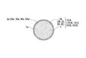
- FIG. 2 is a sectional view taken along line AA in FIG.
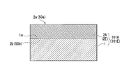
- FIG. 3 is a schematic cross-sectional view of the medical device electrode according to the first embodiment of the present invention.
- the high frequency treatment device 100 of the present embodiment shown in FIG. 1 is an example of the medical device of the present embodiment.
- the high-frequency treatment tool 100 is used for high-frequency treatment of an object to be treated.
- An example of the body to be treated of the high frequency treatment device 100 is a biological tissue.
- Examples of high-frequency treatment performed by the high-frequency treatment device 100 include incision, excision, coagulation (hemostatic), and cauterization of living tissue.
- the high-frequency treatment tool 100 includes a shaft 102 and an electrode portion 101A (medical device electrode).
- the shaft 102 is a support member that supports an electrode unit 101A described later.
- a proximal end of an electrode portion 101A which will be described later, is buried in the distal end (the end portion on the left side in the drawing) of the shaft 102.
- the outer shape of the shaft 102 is a cylinder.
- a conductive portion 104 that is electrically connected to the electrode portion 101A is provided inside the shaft 102.
- the high frequency power source 103 is electrically connected to the conductive portion 104.
- the outer peripheral portion of the shaft 102 is covered with an insulator.
- a hand piece (not shown) is provided at the proximal end (the end portion on the right side in the drawing) of the shaft 102. The handpiece is provided for the purpose of being held by the operator when using the high-frequency treatment instrument 100.
- the electrode portion 101A projects from the distal end of the shaft 102 to the distal side.
- the electrode portion 101A is brought into contact with a living tissue when used.
- the electrode portion 101A is electrically connected to the high frequency power supply 103 by interposing the conductive portion 104.
- the high frequency power source 103 is electrically connected to a counter electrode plate 105 that is attached to the body to be treated.
- the outer shape of the electrode portion 101A is not particularly limited.
- the shape of the protruding portion 101a protruding from the electrode portion 101A in the electrode portion 101A an appropriate shape according to the treatment application of the electrode portion 101A is used.
- the shape of the protruding portion 101a may be a plate shape, a wire shape, a round bar shape, a square bar shape, a disk shape, a hook shape, a radial shape with a plurality of divided tips, or the like.
- the protrusion 101a may extend straight, or may be bent or curved.
- the protrusion 101a may be planar or curved. In the example shown in FIG. 1, the protrusion 101a is formed in the shape of a straight round bar.
- the electrode portion 101A includes an electrode base material 1 (base material) and a film 2A.
- the electrode base material 1 is formed of a metal material.
- the material of the electrode base material 1 is more preferably a metal material having excellent workability. In this case, even if the electrode shape is complicated, it can be easily formed.
- the material of the electrode base material 1 may be different between the central part and the outer peripheral part of the electrode base material 1.
- metal materials suitable for the electrode substrate 1 include stainless steel, aluminum, aluminum alloys, titanium, titanium alloys and the like.
- examples of stainless steel include SUS304 and SUS316.
- the linear expansion coefficient and melting point of SUS304 are 17.3 ⁇ 10 ⁇ 6 K ⁇ 1 and 1400 ° C., respectively.
- linear expansion coefficient and melting point of SUS316 are 16 ⁇ 10 ⁇ 6 K ⁇ 1 and 1371 ° C., respectively. However, each linear expansion coefficient shows a value at 0 to 100 ° C. (the same applies to the following linear expansion coefficients).
- the film 2A is formed on the base material surface 1a (surface of the base material) of the electrode base material 1.
- the film 2A covers at least the entire protrusion 101a.
- the surface 2b of the film 2A is in close contact with the substrate surface 1a.
- the surface 2a opposite to the surface 2b in the thickness direction of the coating film 2A constitutes the outermost surface of the electrode portion 101A in the protruding portion 101a.
- the film 2A contains a first metal and a second metal.
- the first metal includes one or more metals selected from the group consisting of tungsten, tantalum, niobium, and molybdenum.
- the second metal includes at least one metal selected from the group consisting of nickel, titanium, and aluminum.
- the first metal has a high melting point of 2400 ° C. or higher.
- the first metal is contained in the film 2A for the purpose of improving the heat resistance of the film 2A.
- As the first metal a material to which biological tissue is less likely to adhere than the material of the electrode base material 1 is used.
- the melting points of tungsten (W), tantalum (Ta), niobium (Nb), and molybdenum (Mo) are 3400 ° C., 2990 ° C., 2470 ° C., and 2620 ° C., respectively.
- a metal having a high melting point tends to have a coefficient of linear expansion smaller than that of a metal having a low melting point.
- the linear expansion coefficients of tungsten, tantalum, niobium, and molybdenum are 4.5 ⁇ 10 ⁇ 6 K ⁇ 1 , 6.6 ⁇ 10 ⁇ 6 K ⁇ 1 , and 7.1 ⁇ 10 ⁇ 6 K ⁇ 1, respectively. It is 5.1 ⁇ 10 ⁇ 6 K ⁇ 1 .
- gold (melting point: 1064 ° C.), platinum (melting point: 1770 ° C.), silver (melting point: 962 ° C.), palladium (melting point: 1550 ° C.), nickel (melting point: 1450 ° C.), chromium (melting point: melting point: : 1860 ° C.), copper (melting point: 1083 ° C.), and tin (melting point: 232 ° C.) have linear expansion coefficients of 14.2 ⁇ 10 ⁇ 6 K ⁇ 1 and 9.0 ⁇ 10 ⁇ 6 K ⁇ 1 , respectively.
- the second metal is contained in the coating 2A for the purpose of reducing the difference in linear expansion coefficient between the base material and the coating 2A.
- the linear expansion coefficients of nickel, titanium, and aluminum are 8.9 ⁇ 10 ⁇ 6 K ⁇ 1 , 8.5 ⁇ 10 ⁇ 6 K ⁇ 1 , and 23 ⁇ 10 ⁇ 6 K ⁇ 1 , respectively.
- the film 2A contains a second metal having a linear expansion coefficient lower than that of the first metal. As a result, the substantial coefficient of linear expansion of the coating 2A as a whole is reduced.
- the second metal may be contained in the film 2A so that the difference in linear expansion between the electrode substrate 1 and the film 2A on the substrate surface 1a can be reduced.
- the first metal and the second metal are mixed almost uniformly in the coating film 2A.
- the first metal and the second metal are dispersed according to their content rates.
- the coating film 2A in the present embodiment may be a plating film containing a first metal and a second metal.
- the linear expansion coefficient of the film 2A depends on the uniformity of the mixing of the first metal and the second metal, the respective content ratios of the first metal and the second metal, the atomic species of the first metal and the second metal, and the like. Is also different.
- the linear expansion coefficient of the film 2A is larger than the linear expansion coefficient of the first metal and smaller than the linear expansion coefficient of the second metal.
- the melting temperature of the film 2A is considered to be lower than the melting point of the first metal and higher than the melting point of the second metal.
- the material of the second metal it is more preferable to use a material having a linear expansion coefficient close to that of the electrode base material 1.
- the second metal it is more preferable to select a metal having good adhesion to the electrode base material 1.
- the second metal is more preferably a metal contained in the material of the electrode substrate 1 on the substrate surface 1a.
- the main component of the second metal of the film 2A is more preferably nickel.
- the main component of the first metal is more preferably tungsten. In this case, it is more preferable that the second metal and the first metal are made of nickel and tungsten, respectively.
- the electrode substrate 1 is made of titanium or a titanium alloy
- the main component of the second metal of the film 2A is titanium.
- the electrode base material 1 is made of aluminum or an aluminum alloy
- the main component of the second metal of the coating film 2A is more preferably aluminum.
- the content of the first metal in the coating film 2A is not particularly limited as long as the deterioration of the coating film 2A due to sparks and the durability of the coating film 2A against repeated thermal cycles are good.
- the melting temperature of the film 2A approaches the melting point of the first metal.
- the durability of the film 2A against sparks is improved.
- the linear expansion coefficient of the coating 2A approaches the linear expansion coefficient of the first metal, and as a result, the difference in linear expansion between the electrode base material 1 and the coating 2A on the base material surface 1a increases. To do. As a result, the durability of the film 2A against repeated thermal cycles is reduced.
- the content of the first metal is more preferably 10% by mass or more and 50% by mass or less. It is more preferably 20% by mass or more and 50% by mass or less.
- the thickness of the coating film 2A is not particularly limited as long as the deterioration of the coating film 2A due to sparks and the durability of the coating film 2A against repeated thermal cycles are good. If the thickness of the coating film 2A is too thin, the heat capacity of the coating film 2A becomes too small, and as a result, the coating film 2A easily becomes high in temperature. As a result, melting of the film 2A or melting of the electrode base material 1 on the base material surface 1a is likely to occur. Furthermore, if the thickness of the coating 2A is too thin, the coating 2A is likely to be broken by the stress caused by the difference in the linear expansion coefficient with respect to the electrode base material 1. On the other hand, as the thickness of the coating 2A increases, the durability of the coating 2A improves. However, the cost of the electrode portion 101A increases because the manufacturing of the coating 2A takes time and the material cost of the coating 2A increases. For example, the thickness of the film 2A is more preferably 5 ⁇ m or more and 50 ⁇ m or less.
- the electrode base material 1 is manufactured by processing an appropriate metal material.
- the method for manufacturing the electrode base material 1 include press working, cutting work, and molding work.
- the film 2A is formed on the base material surface 1a of the electrode base material 1.
- plating, sputtering, vapor deposition or the like may be used.
- electrolytic plating it is more preferable to use electrolytic plating because it is easy to increase the content rate of the first metal.
- electroless plating may be used.
- the film 2A When the film 2A is formed by plating, a uniform thin film can be easily formed even if the electrode substrate 1 has a complicated shape or has a curved surface with a small curvature.
- the coating film 2A having a required thickness is formed on the base material surface 1a, the electrode portion 101A is obtained.
- the operation of the high-frequency treatment instrument 100 and the electrode portion 101A having such a configuration will be described.
- the operation and usage of the high-frequency treatment instrument 100 and the electrode portion 101A will be described.
- the treatment using the high-frequency treatment device 100 is performed, for example, in a state where the patient (not shown) is attached with the counter electrode plate 105 and the high-frequency power source 3 applies a high-frequency voltage to the electrode portion 101A.
- the operator brings the electrode portion 101A into contact with a body to be treated such as a portion to be treated of a patient while a high frequency voltage is applied to the electrode portion 101A.
- a high frequency voltage is applied between the electrode portion 101A and the counter electrode 105, a high frequency current is generated between the film 2A and the living tissue. Joule heat is generated when a high-frequency current flows through a living tissue. This causes the water in the living tissue to evaporate rapidly. The living tissue is broken by the pressing force from the electrode portion 101A. When the electrode unit 101A is moved with respect to the living tissue, the living tissue can be incised and excised. When a high frequency current is applied while the electrode portion 101A is pressed against the living tissue, the water in the living tissue is rapidly evaporated, and the living tissue is coagulated in the vicinity of the electrode portion 101A. By pressing the electrode portion 101A against the living tissue, hemostasis and cauterization of the living tissue are possible.
- the operator separates the electrode portion 101A from the body to be treated.
- the film 2A is deteriorated, a part of the biological tissue adheres to the film 2A. If the amount of biological tissue attached to the coating film 2A becomes too large, the high-frequency current required for treatment will not flow at the attachment site. As a result, good treatment cannot be performed. Therefore, when the biological tissue excessively adheres to the film 2A, the biological tissue needs to be removed. When the biological tissue is attached in a state where it cannot be sufficiently removed, the electrode unit 101A reaches the end of its life.
- causes of the biological tissue adhering to the surface of the electrode portion 101A include wear and peeling of the film 2A.
- the consumption of the film 2A means that a part where the electrode base material 1 is exposed appears as a result of the film 2A being melted.
- the biological tissue is much more easily attached than at the portion covered with the film 2A.
- the biological tissue is likely to adhere to the exposed portion of the electrode base material 1.
- the entire surface of the electrode does not reach the melting temperature of the electrode material at the same time.
- an insulating layer derived from living tissue is formed on the electrode surface.
- the peeling of the coating film 2A is likely to occur due to repeated stress acting on the coating film 2A and cracking.
- the film 2A falls off from the substrate surface 1a as a fine peeling piece.
- a portion where the electrode base material 1 is exposed is formed.
- the first metal having a high melting point is included.
- the melting temperature of the film 2A is higher than that of the film made of only the second metal having a lower melting point or the electrode substrate 1 itself.
- the linear expansion coefficient of the coating film 2A is larger than that of the first metal alone by including the first metal and the second metal.
- the linear expansion coefficient of the film 2A approaches the linear expansion coefficient of the base material surface 1a of the electrode base material 1. As a result, the stress generated in the heat cycle of heating and cooling that occurs when the electrode unit 101A is repeatedly used is reduced.
- the breakage of the coating film 2A due to the repeated stress and the peeling from the substrate surface 1a are suppressed.
- the wear and peeling of the film 2A can be suppressed, and as a result, the performance of preventing sticking of biological tissue is improved.
- good treatment performance can be maintained for a long period of time.
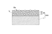
- FIG. 4 is a schematic cross-sectional view of the medical device electrode of the second embodiment of the present invention.
- the electrode portion 101B (medical device electrode) of the present embodiment can be used in place of the electrode portion 101A of the high-frequency treatment device 100 of the first embodiment.
- the electrode portion 101B includes a coating 2B instead of the coating 2A of the electrode portion 101A of the first embodiment.
- the points different from the first embodiment will be mainly described.
- the film 2B of the present embodiment includes a metal film 21 and non-adhesive particles 22.
- the metal film 21 is configured similarly to the film 2A of the first embodiment. However, as for the content rate of the first metal and the content rate of the second metal in the metal film 21, the content rate with respect to the entire coating film 2B is more preferably within the range exemplified in the first embodiment.
- the non-adhesive particles 22 are dispersed in the metal film 21.
- the non-adhesive particles 22 are particles that are excellent in non-adhesiveness to a living tissue.
- the non-adhesive particles 22 may be non-metal inorganic particles or organic particles.
- the non-adhesive particles 22 dispersed in the metal film 21 may be composed of inorganic particles and organic particles.
- the material of the non-adhesive particles 22 dispersed in the metal film 21 may be two or more kinds.
- Examples of the non-adhesive particles 22 include silica particles made of silica chemically modified with a methyl group, PTFE particles made of PTFE (polytetrafluoroethylene), and the like.
- silica particles made of silica chemically modified with a methyl group since the methyl group has a hydrophobic group, it is excellent in non-adhesiveness to a living tissue.
- the non-adhesive particles 22 are used for the purpose of further suppressing attachment of biological tissue on the surface 20a of the electrode portion 101B. Therefore, in the coating film 2B, at least a part of the non-adhesive particles 22 is exposed on the surface 20a.
- the non-adhesive particles 22 may be composed only of particles that are partially embedded in the metal film 21 on the surface 20 a. However, as shown in FIG. 4, it is more preferable that some particles of the non-adhesive particles 22 are distributed inside the metal film 21 without being exposed to the surface 20a.
- the particle size of the non-adhesive particles 22 may be 0.5 ⁇ m or more and 30 ⁇ m or less. If the particle size of the non-adhesive particles 22 is less than 0.5 ⁇ m, the non-adhesive effect may not be sufficiently exhibited due to the small proportion of the non-adhesive particles 22 exposed on the surface. When the particle size of the non-adhesive particles 22 exceeds 30 ⁇ m, the metal film 21 may be broken because peeling easily occurs at the interface between the metal film 21 and the non-adhesive particles 22.
- the particle size of the non-adhesive particles 22 is more preferably 1 ⁇ m or more and 10 ⁇ m or less.
- the non-adhesive particles 22 are likely to appropriately project from the surface of the metal film 21. As a result, a non-adhesive effect due to unevenness can be expected.
- the content of the non-adhesive particles 22 may be 0.5 vol% or more and 20 vol% or less. When the content of the non-adhesive particles 22 is less than 0.5 vol%, the non-adhesive effect may not be sufficiently exhibited due to the small proportion of the non-adhesive particles 22 exposed on the surface of the metal film 21. There is. If the content of the non-adhesive particles 22 exceeds 20 vol%, the practical strength may not be obtained due to the decrease in the film strength of the metal film 21.
- the content of the non-adhesive particles 22 is more preferably 1 vol% or more and 10 vol% or less.
- the electrode part 101B described above can be manufactured in the same manner as in the first embodiment except that the non-adhesive particles 22 are contained in the coating film 2B.
- the film 2B is more preferably formed by electrolytic plating in that the non-adhesive particles 22 are easily dispersed in the film 2B.
- electrolytic plating is performed with the non-adhesive particles 22 dispersed in the plating bath.
- the non-adhesive particles 22 floating in the plating bath move to the surface of the electrode base material 1 together with the metal ions moving in the plating bath.
- the non-adhesive particles 22 are fixed to the deposition surface together with the metal when the metal ions are deposited as the metal.
- the electrode portion 101B By using the electrode portion 101B having such a configuration in place of the electrode portion 101A in the high frequency treatment instrument 100, the same high frequency treatment as that of the electrode portion 101A can be performed.
- the electrode portion 101B includes the metal film 21 similar to the coating film 2A in the first embodiment, and therefore, like the electrode portion 101A, good treatment performance can be maintained for a long period of time. Further, in the electrode portion 101B, the non-adhesive particles 22 that are hard to adhere to the biological tissue are exposed in a dispersed state on the surface 20a of the film 2B. As a result, the coating film 2B further improves the performance of preventing adhesion to the living tissue, as compared with the case where only the metal film 21 contacts the living tissue. In this way, the wear and peeling of the film 2B are suppressed, and as a result, the electrode portion 101B can maintain good treatment performance for a long period of time.
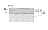
- FIG. 5 is a schematic cross-sectional view of the medical device electrode according to the third embodiment of the present invention.
- the electrode portion 101C (medical device electrode) of the present embodiment can be used in place of the electrode portion 101A of the high-frequency treatment device 100 of the first embodiment.
- the electrode portion 101C includes a coating 2C instead of the coating 2A of the electrode portion 101A of the first embodiment.
- the points different from the first embodiment will be mainly described.
- the film 2C of the present embodiment includes a first metal layer 31 and a second metal layer 32.
- the first metal layer 31 and the second metal layer 32 are laminated in this order from the base material surface 1a. That is, the second metal layer 32 is laminated on the base material surface 1 a of the electrode base material 1.
- the first metal layer 31 is laminated on the surface 30b of the second metal layer 32, which is opposite to the base material surface 1a.
- the surface 30a of the first metal layer 31 opposite to the surface 30b constitutes the outermost surface of the electrode portion 101C.
- the first metal layer 31 is a metal film containing the first metal as a main component metal.
- the first metal layer 31 may include at least one of organic particles and non-metal inorganic particles.
- the first metal layer 31 may include the non-adhesive particles 22 according to the second embodiment. In this case, at least a part of the non-adhesive particles 22 is dispersed in the first metal layer 31 so as to be exposed on the surface 30a.
- the metal component in the first metal layer 31 may be formed of only the first metal.
- the first metal layer 31 may be formed of tungsten only.
- the second metal layer 32 is a metal film containing a second metal as a main component metal.
- the second metal layer 32 may include at least one of organic particles and non-metal inorganic particles.
- the second metal layer 32 is a metal film containing a second metal as a main component metal.
- the metal component in the second metal layer 32 may be formed of only the second metal.
- the second metal layer 32 may be formed of nickel only.
- the thicknesses of the first metal layer 31 and the second metal layer 32 are not particularly limited as long as the durability required for the film 2C is obtained.
- the respective thicknesses of the first metal layer 31 and the second metal layer 32 may be appropriately determined according to the materials and contents of the first metal and the second metal. For example, for simplicity, consider a case where the first metal layer 31 is made of only the first metal and the second metal layer 32 is made of only the second metal. In this case, since the surface 30a is formed of only the first metal, the first metal layer 31 is difficult to melt even if the first metal layer 31 is thin. Further, the second metal layer 32 is made of only the second metal having a larger linear expansion coefficient than the first metal and a smaller linear expansion coefficient than the electrode base material 1. As a result, the thicker the second metal layer 32, the easier the internal strain of the coating film 2C caused by the difference in the linear expansion amount between the electrode base material 1 and the first metal layer 31 becomes.
- the contents of the first metal and the second metal in the film 2C are not particularly limited as long as the durability required for the film 2C is obtained.
- the electrode portion 101C described above is manufactured by stacking the second metal layer 32 and the first metal layer 31 in this order on the base material surface 1a of the electrode base material 1 manufactured in the same manner as in the first embodiment. it can.
- the second metal layer 32 and the first metal layer 31 can be formed by the same forming method as that of the film 2A of the first embodiment.
- the same high frequency treatment as that of the electrode portion 101A can be performed.
- the outermost surface is provided with the first metal layer 31 containing the high melting point first metal as a main component, so that the wear of the film 2C is suppressed.
- the second metal layer 32 having a linear expansion coefficient larger than that of the first metal layer 31 is laminated between the first metal layer 31 and the electrode base material 1, so that the peeling of the coating film 2C occurs. Suppressed. In this way, the consumption and peeling of the film 2C are suppressed, and as a result, the electrode portion 101C can maintain good treatment performance for a long period of time.
- the electrode portion 101D (medical device electrode) of the present embodiment can be used in place of the electrode portion 101A of the high-frequency treatment device 100 of the first embodiment.
- the electrode unit 101D includes a film 2D instead of the film 2A of the electrode unit 101A of the first embodiment.
- the points different from the first embodiment will be mainly described.
- the film 2D of this embodiment includes an outermost layer 41 and an intermediate layer 42.
- the outermost layer 41 and the intermediate layer 42 are laminated in this order from the substrate surface 1a. That is, the intermediate layer 42 is laminated on the base material surface 1 a of the electrode base material 1.
- the outermost layer 41 is laminated on the surface 40b of the intermediate layer 42 opposite to the surface 1a of the base material.
- a surface 40a of the outermost layer 41 opposite to the surface 40b constitutes an outermost surface of the electrode portion 101D.
- the outermost layer 41 is configured similarly to the coating film 2A in the first embodiment.
- the intermediate layer 42 is provided for the purpose of improving the adhesion between the electrode base material 1 and the outermost layer 41.
- a metal material having good adhesion to both the electrode base material 1 and the outermost layer 41 is used.
- nickel or the like can be cited as a material suitable for the intermediate layer 42.
- the linear expansion coefficient of the intermediate layer 42 is preferably smaller than the linear expansion coefficient of the electrode base material 1 in the vicinity of the base material surface 1a and larger than the linear expansion coefficient of the outermost surface layer 41.
- the electrode portion 101D described above can be manufactured by stacking the intermediate layer 42 and the outermost layer 41 in this order on the base material surface 1a of the electrode base material 1 manufactured in the same manner as in the first embodiment.
- the intermediate layer 42 and the outermost layer 41 can be formed by the same forming method as that of the coating film 2A of the first embodiment.
- the same high frequency treatment as that of the electrode portion 101A can be performed. Since the outermost surface layer 41 having the same configuration as that of the first embodiment is provided on the outermost surface of the electrode portion 101D, the wear and peeling of the film 2D are suppressed as in the first embodiment. Furthermore, in the present embodiment, since the intermediate layer 42 is laminated between the outermost layer 41 and the electrode base material 1, peeling of the film 2D is further suppressed. In this way, the wear and peeling of the film 2D are suppressed, and as a result, the electrode portion 101D can maintain good treatment performance for a long period of time.
- the medical device electrode of the fifth embodiment of the present invention will be described.
- the electrode portion 101E (medical device electrode) of the present embodiment can be used in place of the electrode portion 101A of the high-frequency treatment device 100 of the first embodiment.
- the electrode portion 101E includes a coating 2E instead of the coating 2A of the electrode portion 101A of the first embodiment.
- the points different from the first embodiment will be mainly described.
- the coating film 2E of the present embodiment is composed of a single layer as in the first embodiment.
- the surface 50b of the coating 2E is in close contact with the base material surface 1a, like the surface 2a of the coating 2A in the first embodiment.
- the surface 50a opposite to the surface 50b in the thickness direction of the coating film 2E constitutes the outermost surface of the electrode portion 101E in the protruding portion 101a.
- the composition and thickness of the coating 2E are the same as those of the coating 2A in the first embodiment. However, in the coating film 2E, the composition ratio of the first metal and the second metal changes in the thickness direction of the coating film 2E.
- the composition ratio of the second metal is larger than the composition ratio of the first metal on the surface 50b of the film 2E in contact with the substrate surface 1a and its vicinity.
- the composition ratio of the first metal is larger than the composition ratio of the second metal.
- the surface 50b may be formed of only the second metal.
- the surface 50a may be formed of only the first metal. Between the surfaces 50b and 50a, it is more preferable that the composition ratio of the second metal gradually decreases or increases stepwise from the surface 50b to the surface 50a and the composition ratio of the first metal increases gradually or stepwise. preferable.
- the electrode part 101E described above can be manufactured by laminating the coating film 2E in this order on the base material surface 1a of the electrode base material 1 manufactured in the same manner as in the first embodiment.
- the film 2E can be formed by the same forming method as the film 2A of the first embodiment except that the composition ratio of the first metal and the second metal in the thickness direction is changed. From the viewpoint that the composition ratio of the first metal and the second metal can be easily changed, sputtering, vapor deposition, etc. are particularly suitable as the method for forming the coating film 2E.
- the same high frequency treatment as that of the electrode portion 101A can be performed.
- the composition ratio of the high melting point first metal is large on the outermost surface, so that the wear of the film 2E is suppressed.
- the composition ratio of the second metal is large on the surface 50b that is in close contact with the electrode base material 1, so peeling of the coating film 2E is suppressed.
- the linear expansion coefficient changes in the thickness direction as a result of the change in the composition ratio of the first metal and the second metal in the thickness direction.
- the linear expansion coefficient of the surface 50b and its vicinity is larger than the linear expansion coefficient of the surface 50a and its vicinity.
- the linear expansion coefficient of the surface 50b and its vicinity is closer to the linear expansion coefficient of the base material surface 1a of the electrode base material 1 and its vicinity than the linear expansion coefficient of the surface 50a and its vicinity.
- the strain distribution in the thickness direction of the film 2E becomes smoother than that in the case where the film 2C of the third embodiment has a two-layer structure having different composition ratios.
- the coating film 2E further improves the resistance to the repeated stress caused by the thermal cycle due to heating and cooling.
- the electrode portion 101E can maintain good treatment performance for a long period of time.
- the medical device including the medical device electrode used for high-frequency treatment is a high-frequency treatment tool
- the medical device is not limited to the above-described high-frequency treatment tool as long as it includes the electrode for a medical device used for high-frequency treatment.
- Examples of other medical devices in which the electrode for medical devices used for the high-frequency treatment of the present invention can be preferably used include a high-frequency knife, a high-frequency scissors knife, an electric scalpel, and a snare.
- Examples 1_1 to 5, Examples 2_1 to 5, Examples 3_1 to 5, Examples 4_1 to 5, Examples 5_1 to 5, Examples 6_1 to 5, Examples 7_1 to 3, and Examples 8_1 to 3 Will be described together with Comparative Example 1.
- the following [Table 1] shows the configurations of the electrode portions of Examples and Comparative Example 1.
- Examples 1_1 to 5 are examples corresponding to the electrode portion 101A of the above-described first embodiment.
- SUS304 which is stainless steel, was used as the material of the electrode base material 1.
- the outer shape of the protruding portion 101a of the electrode base material 1 was a cylinder having an outer diameter of 0.8 mm.
- the film 2A was formed of only the first metal and the second metal.
- the coating 2A did not contain particles.
- Tungsten (W) was used as the first metal of the film 2A.
- Nickel (Ni) was used as the second metal of the film 2A.
- the W content in the coating 2A was set to 5% by mass or more and less than 10% by mass.
- the numerical value of the content rate is not specified here because the numerical value of the content rate varies among a plurality of test samples due to the manufacturing method and the measurement.
- the thickness of the film 2A (described as “film thickness” in [Table 1]) was set to 1 ⁇ m.
- the coating 2A of Example 1_1 having such a configuration was formed by electrolytic plating. Nickel sulfate and sodium tungstate were added to the plating bath. The ratio of sodium tungstate to nickel sulfate and sodium tungstate was set to 5 mol%. Electrode plating was performed in the above plating bath using the electrode substrate 1 as a cathode.
- Ni—W film was formed on the base material surface 1a of the electrode base material 1 by adjusting the energization time and the amount of current.
- the formed Ni-W film was subjected to EDX analysis (energy dispersive X-ray spectrometry), and the W content in the film 2A was 5% by mass or more and less than 10% by mass. It was.
- the electrode portion 101A of Example 1_2 was formed in the same manner as in Example 1_1 except that the thickness of the coating film 2A was 2 ⁇ m.
- the electrode portion 101A of Example 1_3 was formed in the same manner as in Example 1_1 except that the thickness of the coating film 2A was 5 ⁇ m.
- the electrode portion 101A of Example 1_4 was formed in the same manner as in Example 1_1 except that the thickness of the film 2A was 10 ⁇ m.
- the electrode portion 101A of Example 1_5 was formed in the same manner as in Example 1_1 except that the thickness of the coating film 2A was 15 ⁇ m.
- Examples 2_1 to 6_5 are examples corresponding to the electrode portion 101A of the first embodiment described above.
- the electrode portions 101A of Examples 2_1 to 5 were formed in the same manner as Examples 1_1 to 5 except that the W content in the coating film 2A was 10% by mass or more and less than 20% by mass. Such a W content was obtained by setting the ratio of sodium tungstate in the plating bath to 10 mol%.
- the electrode portions 101A of Examples 3_1 to 5 were formed in the same manner as Examples 1_1 to 5 except that the W content in the film 2A was 20% by mass or more and less than 30% by mass. Such a W content was obtained by setting the proportion of sodium tungstate in the plating bath to 20 mol%.
- the electrode portions 101A of Examples 4_1 to 5 were formed in the same manner as Examples 1_1 to 5 except that the W content in the coating 2A was 40% by mass or more and less than 50% by mass. Such a W content was obtained by setting the ratio of sodium tungstate in the plating bath to 40 mol%.
- the electrode portions 101A of Examples 5_1 to 5 were formed in the same manner as Examples 1_1 to 5 except that the W content in the film 2A was 50% by mass or more and less than 60% by mass. Such a W content was obtained by setting the ratio of sodium tungstate in the plating bath to 50 mol%.
- the electrode portions 101A of Examples 6_1 to 5 were formed in the same manner as Examples 1_1 to 5 except that the W content in the film 2A was 60% by mass or more and less than 70% by mass. Such a W content was obtained by setting the proportion of sodium tungstate in the plating bath to 60 mol%.
- Examples 7_1 to 7-3 are examples corresponding to the electrode portion 101B of the second embodiment described above.
- Example 7_1 was an example corresponding to the electrode portion 101B of the second embodiment described above.
- the electrode base material 1 was formed in the same manner as in Example 1_1.
- the metal film 21 of the film 2B was composed of W and Ni.
- the W content in the coating 2B was set to 40% by mass or more and 50% by mass or less, as in Example 4-3.
- Methyl group-modified silica particles (described as "silica” in [Table 1]) were used as the non-adhesive particles 22 (described as "added particles” in [Table 1]) contained in the coating 2B.
- trimethylsilyl-modified type sicastar (registered trademark) (trade name; manufactured by Micromod) having an average particle diameter of 1 ⁇ m was used.
- the content of the non-adhesive particles 22 in the coating 2B was set to 3 vol%.
- the thickness of the coating 2B was set to 5 ⁇ m as in Example 4_3.
- Such a coating 2B was formed by the same electrolytic plating as in Example 4-3 except that the non-adhesive particles 22 were dispersed in the plating bath.
- the electrode portion 101B of Example 7_2 was formed in the same manner as in Example 7_1 except that the thickness of the coating film 2B was 10 ⁇ m.
- the electrode portion 101B of Example 7_3 was formed in the same manner as in Example 7_1 except that the thickness of the film 2B was 15 ⁇ m.
- Example 8_1 to 3 Similar to Examples 7_1 to 3, Examples 8_1 to 3 were set as Examples corresponding to the electrode portion 101B of the second embodiment described above. In the electrode parts 101B of Examples 8_1 to 3-3, PTFE particles having an average particle size of 1 ⁇ m (described as “PTFE” in [Table 1]) were used as the non-adhesive particles 22. It was formed in the same manner as 3.
- Comparative Example 1 was configured in the same manner as Example 1_3, except that the W ratio in the coating was 100%.
- the thickness of the film of Comparative Example 1 was set to 2 ⁇ m.
- the film of Comparative Example 1 was formed by sputtering.
- Each electrode part of each Example and Comparative Example was attached to the high-frequency treatment instrument 100, and then an evaluation test using the high-frequency treatment instrument 100 was performed.
- an evaluation test a solidification mode test, an incision mode test, and a sticking evaluation test were performed.
- the test was continued until it was necessary to remove the living tissue by sticking the living tissue on the electrode portion.
- the power supply condition of the high-frequency treatment instrument 100 was set to the incision mode.
- the incision treatment of the biological tissue by the electrode portion was performed by energizing for 0.5 seconds in the incision mode. After one energization, the energization was stopped for 0.5 seconds. The operation of repeating such an incision treatment 60 times was defined as one cycle.
- the test was continued until it was necessary to remove the living tissue by sticking the living tissue to the electrode portion.
- the durability of the electrode part was evaluated by the number of continuous cycles. Further, after each test, the tissue adhered to the electrode part was removed, and SEM observation and EDX analysis of the surface of the electrode part were performed.
- evaluation result 1 The evaluation results (evaluation result 1) of the solidification mode test are shown in the following [Table 2].
- the thickness of the film is shown in each row (described as "film thickness” in [Table 2]) and the W content is shown in each column, and the evaluation results of each Example and Comparative Example 1 are shown. .
- “5-10” represents “5% by mass or more and less than 10% by mass”.
- the evaluation result “C” of Example 1_1 is described in the column where the “5-10” column and the “1” row intersect.
- the evaluation result “D” of Comparative Example 1 is described in the column where the “100” column and the “2” row intersect.
- Example 2_1 to Example 5 Example 3_1 to Example 5, and Example 4_1, respectively.
- .About.5 Examples 5_1 to 5 and Examples 6_1 to 4 are described.
- the evaluation is “very good” (very good, “A” in [Table 2]), “good” (good, “B” in [Table 2]), “OK” (fair, “Table 2”). C ”),“ poor ”(no good,“ D ”in [Table 2]).
- the rating was defined as "very good” if the test was continued for more than 2 cycles.
- the evaluation was defined as “good” when the test continued for more than one cycle and the second cycle could not be completed.
- the evaluation was defined as “OK” when the test was completed 30 to 60 times in the first cycle.
- the evaluation was defined as “poor” when the test was completed 29 times or less in the first cycle.
- FIG. 6 is an SEM image of the surface of the electrode for medical device of the example.
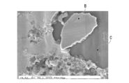
- FIG. 7 is an SEM image of the surface of the medical device electrode of the comparative example.
- the evaluation of Examples 3_3 to 5, Example 4_3 to 5, Example 5_3 to 5, and Example 6_3 to 5 was “very good”.
- the evaluation of Examples 2_3 to 5 was “good”.
- FIG. 6 shows an example of an SEM image of the electrode surface of the example after removing the biological tissue. As can be seen from FIG. 6, the coating on the surface of the electrode of the example was neither cracked nor peeled.
- Example Group X The evaluation of Examples 1_1 to 5, Example 2_1 to 2, Example 3_1 to 2, Example 4_1 to 2 and Examples 5_1 to 2 (hereinafter, abbreviated as Example Group X) was “OK”. It was However, in Example group X, the level was such that it could be reused if the biological tissue was removed. SEM observation of the electrode surface of Example Group X revealed that the coating was thin. There were some areas where the electrode surface was exposed. The evaluation of Examples 6_1 to 5 was “OK” based on the above evaluation criteria. However, when the surface of each electrode of Examples 6_1 to 5 was observed by SEM, peeling of the film was partially observed.
- FIG. 7 shows an SEM image of the electrode surface of Comparative Example 1 after the removal of the biological tissue.
- a peeling piece (denoted by symbol B) in which the film made of W had peeled off was seen, and the substrate surface (denoted by symbol C) was exposed.
- the evaluation result 1 particularly good results were obtained when the W content was 20% by mass or more and less than 60% by mass and the thickness of the film was 5 ⁇ m or more.
- the W content is less than 10% by mass, it is considered that the film was consumed extensively because the area occupied by Ni having a low melting point was too large on the electrode surface.
- Comparative Example 1 was “impossible” as in the solidification mode test. It is considered that, in the electrode portion of Comparative Example 1, even in the incision mode, the adherence of the biological tissue was more likely to occur than in each Example due to the severe wear and peeling of the film.
- [Evaluation result 3] The following [Table 4] shows the evaluation results (evaluation result 3) of Examples 4_3 to 5, Examples 7_1 to 3 and Examples 8_1 to 3 in the sticking evaluation test.
- Example 4 shows the evaluation results of Examples 4_3 to 5.
- Example 7_1 to 3 shows the evaluation results of Examples 7_1 to 3 in the “silica” column.
- PTFE the evaluation results of Examples 8_1 to 3 are shown in the “PTFE” column.
- Each evaluation result in [Table 4] is described by the presence or absence of adhesion of biological tissue. “Present” means that the attachment of the biological tissue was visually observed. “None” means that the attachment of the biological tissue was not visually observed. As shown in [Table 4], in Examples 4_3 to 5 in which the non-adhesive particles 22 were not contained, the biological tissue was attached. However, the adhesion amount was such that there was no hindrance to energization.
- each film in the third to fifth embodiments may include the non-adhesive particles 22 in the second embodiment.
- the second metal layer 32 in the third embodiment may be provided between each film in the first, second, fourth, and fifth embodiments and the electrode base material 1.
- the intermediate layer 42 in the fourth embodiment may be provided between each film in the second, third, and fifth embodiments and the electrode base material.
- an electrode for medical equipment and a medical equipment used for high-frequency treatment that can maintain good treatment performance for a long period of time.
- Electrode base material 1a Surface of base material (surface of base material) 2A, 2B, 2C, 2D, 2E Coating film 21 Metal film 22 Non-adhesive particles 31 First metal layer 32 Second metal layer 41 Outermost layer 42 Intermediate layer 100 High frequency treatment device (medical device) 101a Projection parts 101A, 101B, 101C, 101D, 101B Electrode part (medical device electrode)
Landscapes
- Health & Medical Sciences (AREA)
- Surgery (AREA)
- Engineering & Computer Science (AREA)
- Life Sciences & Earth Sciences (AREA)
- Biomedical Technology (AREA)
- Otolaryngology (AREA)
- Nuclear Medicine, Radiotherapy & Molecular Imaging (AREA)
- Plasma & Fusion (AREA)
- Physics & Mathematics (AREA)
- Heart & Thoracic Surgery (AREA)
- Medical Informatics (AREA)
- Molecular Biology (AREA)
- Animal Behavior & Ethology (AREA)
- General Health & Medical Sciences (AREA)
- Public Health (AREA)
- Veterinary Medicine (AREA)
- Surgical Instruments (AREA)
Abstract
高周波処置に用いられる医療機器用電極は、金属製の基材と、基材の表面に形成された皮膜と、を含む。皮膜は、第1金属と第2金属とを含んでいる。第1金属は、タングステン、タンタル、ニオブ、およびモリブデンからなる群から選ばれた1以上の金属を含む。第2金属は、ニッケル、チタン、およびアルミニウムからなる群から選ばれた1以上の金属を含む。
Description
本発明は、高周波処置に用いられる医療機器用電極および医療機器に関する。
本願は、2018年10月18日に日本に出願された特願2018-197008号に基づき優先権を主張し、その内容をここに援用する。
本願は、2018年10月18日に日本に出願された特願2018-197008号に基づき優先権を主張し、その内容をここに援用する。
高周波処置に使用される医療機器用電極は、生体組織に高周波電流を印加する。高周波電流が印加された生体組織においては、水分が蒸発し、タンパク質が変性する。このような生体組織の一部は、医療機器用電極に付着しやすい。医療機器用電極に付着した生体組織は、医療機器の処置性能を低下させる。
特許文献1には、バイポーラピンセットの先端チップ部へのタンパク質の付着量および固着量を低下させる目的で、先端チップ部に複合メッキ皮膜と積層メッキ皮膜とを積層させる技術が記載されている。複合メッキ皮膜は、貴金属材料と、電気的および熱的な伝導性が低い非伝導性微粒子とからなる。積層メッキ皮膜は、貴金属材料からなる。
特許文献1には、貴金属材料として、金、白金、銀、パラジウム、ニッケル、クロム、銅、およびスズが記載されている。非伝導性微粒子として、ポリテトラフルオロエチレン(PTFE)粒子およびフッ化エチレン重合体粒子が記載されている。
特許文献1には、バイポーラピンセットの先端チップ部へのタンパク質の付着量および固着量を低下させる目的で、先端チップ部に複合メッキ皮膜と積層メッキ皮膜とを積層させる技術が記載されている。複合メッキ皮膜は、貴金属材料と、電気的および熱的な伝導性が低い非伝導性微粒子とからなる。積層メッキ皮膜は、貴金属材料からなる。
特許文献1には、貴金属材料として、金、白金、銀、パラジウム、ニッケル、クロム、銅、およびスズが記載されている。非伝導性微粒子として、ポリテトラフルオロエチレン(PTFE)粒子およびフッ化エチレン重合体粒子が記載されている。
しかしながら、上記のような関連技術には、以下のような問題がある。
高周波処置においては、電極からの強いスパークが発生する。しかし、特許文献1に記載の技術では、スパークによって電極の表面が局所的に溶融しやすい。この理由は、スパークに起因する発熱によって、電極表面の一部の温度がメッキ皮膜中の貴金属材料の融点を超えるからである。メッキ皮膜の一部が溶融すると、メッキ皮膜の厚さが低下する結果、電極基材が露出する。電極基材が露出すると生体組織の付着量が増大する。この結果、電極の寿命が低下する。
電極寿命を延ばす目的で、電極表面に高融点の金属材料の皮膜を形成することも考えられる。例えば、3400℃の融点を有するタングステンの皮膜を形成すると、スパークによる電極の溶融は起こりにくくなる。
しかし、電極は使用時に加熱され使用後に冷却される。この結果、電極は、熱応力による繰り返し負荷を受ける。繰り返し負荷を受ける結果、電極基材と高融点の金属材料との線膨張係数の差によって皮膜のはがれが起こりやすくなる。皮膜がはがれた部位では、生体組織の付着が発生しやすくなる結果、電極の寿命が低下する。
例えば、電極基材に用いられることが多いステンレス鋼の線膨張係数は17.3×10⁻⁶K-1である。これに対して、タングステンの線膨張係数はステンレス鋼の約1/4である。
高周波処置においては、電極からの強いスパークが発生する。しかし、特許文献1に記載の技術では、スパークによって電極の表面が局所的に溶融しやすい。この理由は、スパークに起因する発熱によって、電極表面の一部の温度がメッキ皮膜中の貴金属材料の融点を超えるからである。メッキ皮膜の一部が溶融すると、メッキ皮膜の厚さが低下する結果、電極基材が露出する。電極基材が露出すると生体組織の付着量が増大する。この結果、電極の寿命が低下する。
電極寿命を延ばす目的で、電極表面に高融点の金属材料の皮膜を形成することも考えられる。例えば、3400℃の融点を有するタングステンの皮膜を形成すると、スパークによる電極の溶融は起こりにくくなる。
しかし、電極は使用時に加熱され使用後に冷却される。この結果、電極は、熱応力による繰り返し負荷を受ける。繰り返し負荷を受ける結果、電極基材と高融点の金属材料との線膨張係数の差によって皮膜のはがれが起こりやすくなる。皮膜がはがれた部位では、生体組織の付着が発生しやすくなる結果、電極の寿命が低下する。
例えば、電極基材に用いられることが多いステンレス鋼の線膨張係数は17.3×10⁻⁶K-1である。これに対して、タングステンの線膨張係数はステンレス鋼の約1/4である。
本発明は、上記のような問題に鑑みてなされたものであり、良好な処置性能を長期間維持することができる、高周波処置に用いられる医療機器用電極および医療機器を提供することを目的とする。
上記の課題を解決するために、本発明の第1の態様の高周波処置に用いられる医療機器用電極は、金属製の基材と、前記基材の表面に形成された皮膜と、を備え、前記皮膜は、第1金属と第2金属とを含んでおり、前記第1金属は、タングステン、タンタル、ニオブ、およびモリブデンからなる群から選ばれた1以上の金属を含み、前記第2金属は、ニッケル、チタン、およびアルミニウムからなる群から選ばれた1以上の金属を含む。
本発明の第2の態様の医療機器は、上記医療機器用電極を備える。
本発明の高周波処置に用いられる医療機器用電極および医療機器によれば、良好な処置性能を長期間維持することができる。
以下では、本発明の実施形態について添付図面を参照して説明する。すべての図面において、実施形態が異なる場合であっても、同一または相当する部材には同一の符号を付し、共通する説明は省略する。
[第1の実施形態]
本発明の第1の実施形態の医療機器用電極および医療機器について説明する。
図1は、本発明の第1の実施形態の医療機器の一例を示す模式的な構成図である。図2は、図1におけるA-A断面図である。図3は、本発明の第1の実施形態の医療機器用電極の模式的な断面図である。
本発明の第1の実施形態の医療機器用電極および医療機器について説明する。
図1は、本発明の第1の実施形態の医療機器の一例を示す模式的な構成図である。図2は、図1におけるA-A断面図である。図3は、本発明の第1の実施形態の医療機器用電極の模式的な断面図である。
図1に示す本実施形態の高周波処置具100は、本実施形態の医療機器の一例である。
高周波処置具100は、被処置体に対する高周波処置に用いられる。高周波処置具100の被処置体の例としては、生体組織が挙げられる。高周波処置具100によって行われる高周波処置の例としては、生体組織の切開、切除、凝固(止血)、焼灼などが挙げられる。
高周波処置具100は、シャフト102と、電極部101A(医療機器用電極)と、を備える。
高周波処置具100は、被処置体に対する高周波処置に用いられる。高周波処置具100の被処置体の例としては、生体組織が挙げられる。高周波処置具100によって行われる高周波処置の例としては、生体組織の切開、切除、凝固(止血)、焼灼などが挙げられる。
高周波処置具100は、シャフト102と、電極部101A(医療機器用電極)と、を備える。
シャフト102は、後述する電極部101Aを支持する支持部材である。シャフト102の遠位端(図示左側の端部)には、後述する電極部101Aの近位端が埋没されている。
本実施形態では、シャフト102の外形は円柱である。シャフト102の内部には、電極部101Aに電気的に接続する導電部104が設けられている。導電部104には、高周波電源103が電気的に接続されている。シャフト102の外周部は絶縁体で覆われている。
シャフト102における近位端(図示右側の端部)には、図示略のハンドピースが設けられている。ハンドピースは、高周波処置具100の使用時に術者が手で持つ目的で設けられている。
本実施形態では、シャフト102の外形は円柱である。シャフト102の内部には、電極部101Aに電気的に接続する導電部104が設けられている。導電部104には、高周波電源103が電気的に接続されている。シャフト102の外周部は絶縁体で覆われている。
シャフト102における近位端(図示右側の端部)には、図示略のハンドピースが設けられている。ハンドピースは、高周波処置具100の使用時に術者が手で持つ目的で設けられている。
電極部101Aは、シャフト102の遠位端から遠位側に突出している。電極部101Aは、使用時に生体組織に当接される。電極部101Aは、導電部104が介在することによって高周波電源103に電気的に接続されている。高周波電源103には、被処置体に装着する対極板105が電気的に接続されている。
電極部101Aの外形は特に限定されない。電極部101Aにおいて電極部101Aから突出している突出部101aの形状としては、電極部101Aの処置用途に応じた適宜の形状が用いられる。例えば、突出部101aの形状は、板状、ワイヤー状、丸棒状、角棒状、円板状、鉤状、先端が複数に分かれた放射状などであってもよい。突出部101aの形状が線状の場合、突出部101aは、真直に延びていてもよいし、屈曲または湾曲していてもよい。突出部101aの形状が面状の場合、突出部101aは、平面状であってもよいし、曲面状であってもよい。
図1に示す例では、突出部101aは真直の丸棒状に形成されている。
図1に示す例では、突出部101aは真直の丸棒状に形成されている。
図2に示すように、電極部101Aは、電極基材1(基材)と、皮膜2Aと、を備える。
電極基材1は、金属材料によって形成される。電極基材1の材質は、加工性に優れる金属材料であることがより好ましい。この場合、電極形状が複雑でも、容易に形成できる。
電極基材1の材料は、電極基材1の中心部と外周部とで異なっていてもよい。
電極基材1に好適な金属材料の例としては、ステンレス鋼、アルミニウム、アルミニウム合金、チタン、チタン合金などが挙げられる。
例えば、ステンレス鋼の例としては、SUS304、SUS316などが挙げられる。
SUS304の線膨張係数および融点は、それぞれ、17.3×10⁻⁶K-1、1400℃である。SUS316の線膨張係数および融点は、それぞれ、16×10-6K-1、1371℃である。ただし、各線膨張係数は0-100℃における値を示す(以下の線膨張係数も同様)。
電極基材1は、金属材料によって形成される。電極基材1の材質は、加工性に優れる金属材料であることがより好ましい。この場合、電極形状が複雑でも、容易に形成できる。
電極基材1の材料は、電極基材1の中心部と外周部とで異なっていてもよい。
電極基材1に好適な金属材料の例としては、ステンレス鋼、アルミニウム、アルミニウム合金、チタン、チタン合金などが挙げられる。
例えば、ステンレス鋼の例としては、SUS304、SUS316などが挙げられる。
SUS304の線膨張係数および融点は、それぞれ、17.3×10⁻⁶K-1、1400℃である。SUS316の線膨張係数および融点は、それぞれ、16×10-6K-1、1371℃である。ただし、各線膨張係数は0-100℃における値を示す(以下の線膨張係数も同様)。
皮膜2Aは、電極基材1の基材表面1a(基材の表面)上に形成されている。皮膜2Aは、少なくとも突出部101aの全体を被覆している。図3に示すように、皮膜2Aの表面2bは基材表面1aに密着している。皮膜2Aの厚さ方向において表面2bと反対側の表面2aは、突出部101aにおける電極部101Aの最表面を構成している。
皮膜2Aは、第1金属と第2金属とを含んでいる。第1金属は、タングステン、タンタル、ニオブ、およびモリブデンからなる群から選ばれた1以上の金属を含む。第2金属は、ニッケル、チタン、およびアルミニウムからなる群から選ばれた1以上の金属を含む。
皮膜2Aは、第1金属と第2金属とを含んでいる。第1金属は、タングステン、タンタル、ニオブ、およびモリブデンからなる群から選ばれた1以上の金属を含む。第2金属は、ニッケル、チタン、およびアルミニウムからなる群から選ばれた1以上の金属を含む。
第1金属は、2400℃以上の高融点を有する。第1金属は、皮膜2Aの耐熱性を向上する目的で皮膜2Aに含まれている。第1金属としては、電極基材1の材料に比べて生体組織が付着しにくい材料が用いられる。
タングステン(W)、タンタル(Ta)、ニオブ(Nb)、およびモリブデン(Mo)の融点は、それぞれ、3400℃、2990℃、2470℃、2620℃である。
高融点を有する金属の線膨張係数は、融点が低い金属の線膨張係数よりも小さい傾向がある。
例えば、タングステン、タンタル、ニオブ、およびモリブデンの線膨張係数は、それぞれ、4.5×10⁻⁶K-1、6.6×10⁻⁶K-1、7.1×10⁻⁶K-1、5.1×10⁻⁶K-1である。
これに対して、例えば、金(融点:1064℃)、白金(融点:1770℃)、銀(融点:962℃)、パラジウム(融点:1550℃)、ニッケル(融点:1450℃)、クロム(融点:1860℃)、銅(融点:1083℃)、スズ(融点:232℃)の線膨張係数は、それぞれ、14.2×10⁻⁶K-1、9.0×10⁻⁶K-1、19.3×10⁻⁶K-1、10.6×10⁻⁶K-1、8.9×10⁻⁶K-1、8.4×10⁻⁶K-1、16.7×10⁻⁶K-1、23×10-6K-1である。
タングステン(W)、タンタル(Ta)、ニオブ(Nb)、およびモリブデン(Mo)の融点は、それぞれ、3400℃、2990℃、2470℃、2620℃である。
高融点を有する金属の線膨張係数は、融点が低い金属の線膨張係数よりも小さい傾向がある。
例えば、タングステン、タンタル、ニオブ、およびモリブデンの線膨張係数は、それぞれ、4.5×10⁻⁶K-1、6.6×10⁻⁶K-1、7.1×10⁻⁶K-1、5.1×10⁻⁶K-1である。
これに対して、例えば、金(融点:1064℃)、白金(融点:1770℃)、銀(融点:962℃)、パラジウム(融点:1550℃)、ニッケル(融点:1450℃)、クロム(融点:1860℃)、銅(融点:1083℃)、スズ(融点:232℃)の線膨張係数は、それぞれ、14.2×10⁻⁶K-1、9.0×10⁻⁶K-1、19.3×10⁻⁶K-1、10.6×10⁻⁶K-1、8.9×10⁻⁶K-1、8.4×10⁻⁶K-1、16.7×10⁻⁶K-1、23×10-6K-1である。
第2金属は、基材と皮膜2Aの線膨張係数差を低減する目的で皮膜2Aに含まれている。ニッケル、チタン、およびアルミニウムの線膨張係数は、それぞれ、8.9×10⁻⁶K-1、8.5×10⁻⁶K-1、23×10-6K-1である。
皮膜2Aにおいては、第1金属よりも線膨張係数が低い第2金属が含まれる。この結果、皮膜2A全体としての実質的な線膨張係数が低減される。
第2金属は、基材表面1aにおける電極基材1と皮膜2Aとの線膨張の差が低減される結果が得られるように、皮膜2Aに含まれていればよい。
皮膜2Aにおいては、第1金属よりも線膨張係数が低い第2金属が含まれる。この結果、皮膜2A全体としての実質的な線膨張係数が低減される。
第2金属は、基材表面1aにおける電極基材1と皮膜2Aとの線膨張の差が低減される結果が得られるように、皮膜2Aに含まれていればよい。
例えば、本実施形態では、皮膜2Aにおいて第1金属と第2金属とが略均一に混ざり合っている。皮膜2Aの表面2aには、第1金属および第2金属がそれぞれの含有率に応じて分散している。
例えば、本実施形態における皮膜2Aは、第1金属および第2金属を含むメッキ膜であってもよい。
この場合、皮膜2Aの線膨張係数は、第1金属および第2金属の混ざり方の均一性、第1金属および第2金属の各含有率、第1金属および第2金属の各原子種などによっても異なる。しかし、皮膜2Aの線膨張係数は、第1金属の線膨張係数よりも大きく、第2金属の線膨張係数よりも小さくなると考えられる。
同様に、皮膜2Aの溶融温度は、第1金属の融点よりも低く、第2金属の融点よりも高くなると考えられる。
例えば、本実施形態における皮膜2Aは、第1金属および第2金属を含むメッキ膜であってもよい。
この場合、皮膜2Aの線膨張係数は、第1金属および第2金属の混ざり方の均一性、第1金属および第2金属の各含有率、第1金属および第2金属の各原子種などによっても異なる。しかし、皮膜2Aの線膨張係数は、第1金属の線膨張係数よりも大きく、第2金属の線膨張係数よりも小さくなると考えられる。
同様に、皮膜2Aの溶融温度は、第1金属の融点よりも低く、第2金属の融点よりも高くなると考えられる。
第2金属の材料としては、電極基材1の線膨張係数に近い線膨張係数を有する材料が用いられることがより好ましい。
第2金属は、電極基材1との密着性が良好な金属が選ばれることがより好ましい。例えば、第2金属は、基材表面1aにおける電極基材1の材料に含有される金属であることがより好ましい。
例えば、電極基材1がステンレス鋼からなる場合には、皮膜2Aの第2金属の主成分は、ニッケルであることがより好ましい。電極基材1がステンレス鋼、第2金属の主成分がニッケルである場合、第1金属の主成分としては、タングステンであることがより好ましい。この場合、第2金属、第1金属は、それぞれニッケル、タングステンからなることがさらに好ましい。
例えば、電極基材1がチタンまたはチタン合金からなる場合には、皮膜2Aの第2金属の主成分は、チタンであることがより好ましい。例えば、電極基材1がアルミニウムまたはアルミニウム合金からなる場合には、皮膜2Aの第2金属の主成分は、アルミニウムであることがより好ましい。
第2金属は、電極基材1との密着性が良好な金属が選ばれることがより好ましい。例えば、第2金属は、基材表面1aにおける電極基材1の材料に含有される金属であることがより好ましい。
例えば、電極基材1がステンレス鋼からなる場合には、皮膜2Aの第2金属の主成分は、ニッケルであることがより好ましい。電極基材1がステンレス鋼、第2金属の主成分がニッケルである場合、第1金属の主成分としては、タングステンであることがより好ましい。この場合、第2金属、第1金属は、それぞれニッケル、タングステンからなることがさらに好ましい。
例えば、電極基材1がチタンまたはチタン合金からなる場合には、皮膜2Aの第2金属の主成分は、チタンであることがより好ましい。例えば、電極基材1がアルミニウムまたはアルミニウム合金からなる場合には、皮膜2Aの第2金属の主成分は、アルミニウムであることがより好ましい。
皮膜2Aにおける第1金属の含有率は、スパークによる皮膜2Aの劣化と、繰り返しの熱サイクルに対する皮膜2Aの耐久性と、が良好になれば、特に限定されない。
第1金属の含有率が増加すると、皮膜2Aの溶融温度が第1金属の融点に近づく。この結果、スパークに対する皮膜2Aの耐久性は向上する。
一方、第1金属の含有率が増加すると、皮膜2Aの線膨張係数が第1金属の線膨張係数に近づく結果、基材表面1aにおける電極基材1と皮膜2Aとの線膨張の差が増大する。この結果、繰り返しの熱サイクルに対する皮膜2Aの耐久性は低下する。
スパークに対する皮膜2Aの耐久性と、繰り返しの熱サイクルに対する皮膜2Aの耐久性とのバランスを良好にする目的では、第1金属の含有率は、10質量%以上50質量%以下であることがより好ましく、20質量%以上50質量%以下であることがさらに好ましい。
第1金属の含有率が増加すると、皮膜2Aの溶融温度が第1金属の融点に近づく。この結果、スパークに対する皮膜2Aの耐久性は向上する。
一方、第1金属の含有率が増加すると、皮膜2Aの線膨張係数が第1金属の線膨張係数に近づく結果、基材表面1aにおける電極基材1と皮膜2Aとの線膨張の差が増大する。この結果、繰り返しの熱サイクルに対する皮膜2Aの耐久性は低下する。
スパークに対する皮膜2Aの耐久性と、繰り返しの熱サイクルに対する皮膜2Aの耐久性とのバランスを良好にする目的では、第1金属の含有率は、10質量%以上50質量%以下であることがより好ましく、20質量%以上50質量%以下であることがさらに好ましい。
皮膜2Aの厚さは、スパークによる皮膜2Aの劣化と、繰り返しの熱サイクルに対する皮膜2Aの耐久性と、が良好になれば、特に限定されない。
皮膜2Aの厚さが薄すぎると、皮膜2Aの熱容量が小さくなりすぎる結果、皮膜2Aが高温になりやすくなる。この結果、皮膜2Aの溶融または基材表面1aにおける電極基材1の溶融が起こりやすくなる。
さらに、皮膜2Aの厚さが薄すぎると、電極基材1に対する線膨張係数の差に起因する応力によって皮膜2Aが破断されやすくなる。
一方、皮膜2Aの厚さが増大すると、皮膜2Aの耐久性は向上する。しかし、皮膜2Aの製造に時間がかかる、皮膜2Aの材料費が増大する、といった理由で、電極部101Aのコストが増大してしまう。
例えば、皮膜2Aの厚さは、5μm以上50μm以下であることがより好ましい。
皮膜2Aの厚さが薄すぎると、皮膜2Aの熱容量が小さくなりすぎる結果、皮膜2Aが高温になりやすくなる。この結果、皮膜2Aの溶融または基材表面1aにおける電極基材1の溶融が起こりやすくなる。
さらに、皮膜2Aの厚さが薄すぎると、電極基材1に対する線膨張係数の差に起因する応力によって皮膜2Aが破断されやすくなる。
一方、皮膜2Aの厚さが増大すると、皮膜2Aの耐久性は向上する。しかし、皮膜2Aの製造に時間がかかる、皮膜2Aの材料費が増大する、といった理由で、電極部101Aのコストが増大してしまう。
例えば、皮膜2Aの厚さは、5μm以上50μm以下であることがより好ましい。
以上説明した電極部101Aは、例えば、以下のようにして製造されてもよい。
例えば、適宜の金属材料が加工されて電極基材1が製造される。電極基材1の製造方法としては、例えば、プレス加工、切削加工、成形加工などが挙げられる。
この後、電極基材1の基材表面1aに皮膜2Aが形成される。
皮膜2Aの形成方法としては、例えば、メッキ、スパッタリング、蒸着などが用いられてもよい。
皮膜2Aがメッキによって形成される場合、第1金属の含有率を増やしやすい点で、電解メッキが用いられることがより好ましい。ただし、第1金属の含有率が低くてもよい場合には、無電解メッキが用いられてもよい。
皮膜2Aがメッキによって形成される場合、電極基材1の形状が複雑であったり、曲率の小さな湾曲面を有していたりしても、均一な薄膜が容易に形成される。
基材表面1a上に、必要な厚さの皮膜2Aが形成されると、電極部101Aが得られる。
例えば、適宜の金属材料が加工されて電極基材1が製造される。電極基材1の製造方法としては、例えば、プレス加工、切削加工、成形加工などが挙げられる。
この後、電極基材1の基材表面1aに皮膜2Aが形成される。
皮膜2Aの形成方法としては、例えば、メッキ、スパッタリング、蒸着などが用いられてもよい。
皮膜2Aがメッキによって形成される場合、第1金属の含有率を増やしやすい点で、電解メッキが用いられることがより好ましい。ただし、第1金属の含有率が低くてもよい場合には、無電解メッキが用いられてもよい。
皮膜2Aがメッキによって形成される場合、電極基材1の形状が複雑であったり、曲率の小さな湾曲面を有していたりしても、均一な薄膜が容易に形成される。
基材表面1a上に、必要な厚さの皮膜2Aが形成されると、電極部101Aが得られる。
次に、このような構成の高周波処置具100および電極部101Aの作用について説明する。
まず、高周波処置具100および電極部101Aの動作および使用方法について説明する。
図1に示すように、高周波処置具100を用いた処置は、例えば、患者(図示略)に対極板105を装着し、高周波電源3によって電極部101Aに高周波電圧を印加した状態で行われる。術者は、電極部101Aに高周波電圧を印加した状態で、患者の被処置部などの被処置体に電極部101Aを接触させる。
電極部101Aと対極板105との間に高周波電圧が印加されると、皮膜2Aと生体組織との間に高周波電流が発生する。高周波電流が生体組織に流れるとジュール熱が発生する。これにより生体組織の水分が急速に蒸発する。生体組織は、電極部101Aからの押圧力によって破断される。電極部101Aが生体組織に対して移動されると、生体組織の切開、切除が可能となる。
電極部101Aを生体組織に押し当てた状態で高周波電流が流されると、生体組織の水分が急速に蒸発し、電極部101Aの近傍で生体組織が凝固される。電極部101Aが生体組織に押し当てられることにより、止血や生体組織の焼灼が可能となる。
必要な処置が終了すると、術者は、電極部101Aを被処置体から離間させる。このとき、皮膜2Aが劣化していると、生体組織の一部が皮膜2Aに付着する。皮膜2Aへの生体組織の付着量が多くなりすぎると、付着部位において処置に必要な高周波電流が流れなくなる。この結果、良好な処置が遂行できなくなる。
したがって、皮膜2Aに生体組織が過剰に付着した場合には、生体組織が除去される必要がある。生体組織が充分除去できない状態で付着している場合には、電極部101Aは寿命を迎える。
まず、高周波処置具100および電極部101Aの動作および使用方法について説明する。
図1に示すように、高周波処置具100を用いた処置は、例えば、患者(図示略)に対極板105を装着し、高周波電源3によって電極部101Aに高周波電圧を印加した状態で行われる。術者は、電極部101Aに高周波電圧を印加した状態で、患者の被処置部などの被処置体に電極部101Aを接触させる。
電極部101Aと対極板105との間に高周波電圧が印加されると、皮膜2Aと生体組織との間に高周波電流が発生する。高周波電流が生体組織に流れるとジュール熱が発生する。これにより生体組織の水分が急速に蒸発する。生体組織は、電極部101Aからの押圧力によって破断される。電極部101Aが生体組織に対して移動されると、生体組織の切開、切除が可能となる。
電極部101Aを生体組織に押し当てた状態で高周波電流が流されると、生体組織の水分が急速に蒸発し、電極部101Aの近傍で生体組織が凝固される。電極部101Aが生体組織に押し当てられることにより、止血や生体組織の焼灼が可能となる。
必要な処置が終了すると、術者は、電極部101Aを被処置体から離間させる。このとき、皮膜2Aが劣化していると、生体組織の一部が皮膜2Aに付着する。皮膜2Aへの生体組織の付着量が多くなりすぎると、付着部位において処置に必要な高周波電流が流れなくなる。この結果、良好な処置が遂行できなくなる。
したがって、皮膜2Aに生体組織が過剰に付着した場合には、生体組織が除去される必要がある。生体組織が充分除去できない状態で付着している場合には、電極部101Aは寿命を迎える。
電極部101Aの表面に生体組織が付着する原因としては、皮膜2Aの消耗およびはがれが挙げられる。
ここで、皮膜2Aの消耗とは、皮膜2Aが溶融する結果、電極基材1が露出する部位が現れることを意味する。電極基材1が露出する部位では、皮膜2Aに覆われた部位に比べて、生体組織が格段に付着しやすい。この結果、生体組織が電極基材1の露出する部位に固着しやすい。
高周波処置においては、電極の表面全体が同時に電極材料の溶融温度に達することはない。しかし、生体組織において、ジュール熱による水分の蒸発およびタンパク質の変性が生じると、電極表面に生体組織由来の絶縁層が形成される。この状態でさらに高周波電圧が印加されると、絶縁層を介して電極表面から放電が起こる。大きな高周波電力を要する高周波処置では、このような放電はスパークを引き起こす。スパーク電流は、微小領域に集中するので、電極表面の一部に局所的な高温部が生じる。このような高温部では、電極材料の溶融温度を超えることがあると考えられる。
ここで、皮膜2Aの消耗とは、皮膜2Aが溶融する結果、電極基材1が露出する部位が現れることを意味する。電極基材1が露出する部位では、皮膜2Aに覆われた部位に比べて、生体組織が格段に付着しやすい。この結果、生体組織が電極基材1の露出する部位に固着しやすい。
高周波処置においては、電極の表面全体が同時に電極材料の溶融温度に達することはない。しかし、生体組織において、ジュール熱による水分の蒸発およびタンパク質の変性が生じると、電極表面に生体組織由来の絶縁層が形成される。この状態でさらに高周波電圧が印加されると、絶縁層を介して電極表面から放電が起こる。大きな高周波電力を要する高周波処置では、このような放電はスパークを引き起こす。スパーク電流は、微小領域に集中するので、電極表面の一部に局所的な高温部が生じる。このような高温部では、電極材料の溶融温度を超えることがあると考えられる。
皮膜2Aのはがれは、皮膜2Aに繰り返し応力が作用して亀裂が生じることによって発生しやすくなる。この場合、皮膜2Aは微細な剥離片として基材表面1aから脱落する。
この結果、電極基材1が露出する部位が形成される。
この結果、電極基材1が露出する部位が形成される。
本実施形態の皮膜2Aによれば、高融点を有する第1金属を含んでいる。この結果、より低融点の第2金属のみからなる皮膜あるいは電極基材1自体に比べて、皮膜2Aの溶融温度が高くなっている。この結果、使用時におけるスパークに起因する温度上昇が生じても、皮膜2Aの溶融が起こりにくくなっている。
さらに、皮膜2Aによれば、第1金属および第2金属を含むことによって、第1金属単体よりも、皮膜2Aの線膨張係数が大きくなっている。この結果、皮膜2Aの線膨張係数が電極基材1の基材表面1aにおける線膨張係数に近づいている。これにより、電極部101Aが繰り返し使用される際に発生する加熱および冷却の熱サイクルにおいて発生する応力が低減される。この結果、繰り返し応力に起因する皮膜2Aの破断と、基材表面1aに対する剥離と、が抑制される。
このようにして、電極部101Aでは、皮膜2Aの消耗およびはがれが抑制できる結果、生体組織の固着防止性能が向上する。
この結果、本実施形態の高周波処置具100および電極部101Aによれば、良好な処置性能を長期間維持することができる。
さらに、皮膜2Aによれば、第1金属および第2金属を含むことによって、第1金属単体よりも、皮膜2Aの線膨張係数が大きくなっている。この結果、皮膜2Aの線膨張係数が電極基材1の基材表面1aにおける線膨張係数に近づいている。これにより、電極部101Aが繰り返し使用される際に発生する加熱および冷却の熱サイクルにおいて発生する応力が低減される。この結果、繰り返し応力に起因する皮膜2Aの破断と、基材表面1aに対する剥離と、が抑制される。
このようにして、電極部101Aでは、皮膜2Aの消耗およびはがれが抑制できる結果、生体組織の固着防止性能が向上する。
この結果、本実施形態の高周波処置具100および電極部101Aによれば、良好な処置性能を長期間維持することができる。
[第2の実施形態]
本発明の第2の実施形態の医療機器用電極について説明する。
図4は、本発明の第2の実施形態の医療機器用電極の模式的な断面図である。
本発明の第2の実施形態の医療機器用電極について説明する。
図4は、本発明の第2の実施形態の医療機器用電極の模式的な断面図である。
図1に示すように、本実施形態の電極部101B(医療機器用電極)は、第1の実施形態の高周波処置具100における電極部101Aに代えて用いることができる。
図2、4に示すように、電極部101Bは、第1の実施形態の電極部101Aの皮膜2Aに代えて、皮膜2Bを備える。
以下、第1の実施形態と異なる点を中心に説明する。
図2、4に示すように、電極部101Bは、第1の実施形態の電極部101Aの皮膜2Aに代えて、皮膜2Bを備える。
以下、第1の実施形態と異なる点を中心に説明する。
図4に示すように、本実施形態の皮膜2Bは、金属膜21と、非粘着性粒子22と、を備える。
金属膜21は、第1の実施形態の皮膜2Aと同様に構成される。ただし、金属膜21における第1金属の含有率および第2金属の含有率は、皮膜2B全体に対する含有率が第1の実施形態に例示された範囲であることがより好ましい。
非粘着性粒子22は、金属膜21に分散されている。非粘着性粒子22は、生体組織に対する非粘着性に優れる粒子からなる。例えば、非粘着性粒子22は、非金属の無機粒子であってもよいし、有機粒子であってもよい。金属膜21に分散される非粘着性粒子22は、無機粒子および有機粒子で構成されてもよい。金属膜21に分散される非粘着性粒子22の材質は、2種類以上であってもよい。
非粘着性粒子22の例としては、メチル基で化学修飾されたシリカからなるシリカ粒子、PTFE(ポリテトラフルオロエチレン)からなるPTFE粒子などが挙げられる。例えば、メチル基で化学修飾されたシリカ粒子の場合、メチル基が疎水基を有する結果、生体組織への非粘着性に優れる。例えば、PTFE粒子の場合、フッ素樹脂自体が疎水性を有する結果、生体組織への非粘着性に優れる。
非粘着性粒子22は、電極部101Bの表面20aにおける生体組織の付着をさらに抑制する目的で用いられる。したがって、皮膜2Bにおいて、非粘着性粒子22の少なくとも一部は、表面20aに露出している。
例えば、非粘着性粒子22は、表面20aにおいて、一部が金属膜21に埋没された粒子のみで構成されてもよい。
ただし、図4に示すように、非粘着性粒子22の一部の粒子は、表面20aに露出することなく金属膜21の内部に分布していることがより好ましい。この場合、経時使用によって、金属膜21の厚さが減少しても、内部に分布する非粘着性粒子22が表面に露出する。この結果、金属膜21の厚さが減少しても、非粘着性粒子22による生体組織の付着防止性能が持続される。
金属膜21は、第1の実施形態の皮膜2Aと同様に構成される。ただし、金属膜21における第1金属の含有率および第2金属の含有率は、皮膜2B全体に対する含有率が第1の実施形態に例示された範囲であることがより好ましい。
非粘着性粒子22は、金属膜21に分散されている。非粘着性粒子22は、生体組織に対する非粘着性に優れる粒子からなる。例えば、非粘着性粒子22は、非金属の無機粒子であってもよいし、有機粒子であってもよい。金属膜21に分散される非粘着性粒子22は、無機粒子および有機粒子で構成されてもよい。金属膜21に分散される非粘着性粒子22の材質は、2種類以上であってもよい。
非粘着性粒子22の例としては、メチル基で化学修飾されたシリカからなるシリカ粒子、PTFE(ポリテトラフルオロエチレン)からなるPTFE粒子などが挙げられる。例えば、メチル基で化学修飾されたシリカ粒子の場合、メチル基が疎水基を有する結果、生体組織への非粘着性に優れる。例えば、PTFE粒子の場合、フッ素樹脂自体が疎水性を有する結果、生体組織への非粘着性に優れる。
非粘着性粒子22は、電極部101Bの表面20aにおける生体組織の付着をさらに抑制する目的で用いられる。したがって、皮膜2Bにおいて、非粘着性粒子22の少なくとも一部は、表面20aに露出している。
例えば、非粘着性粒子22は、表面20aにおいて、一部が金属膜21に埋没された粒子のみで構成されてもよい。
ただし、図4に示すように、非粘着性粒子22の一部の粒子は、表面20aに露出することなく金属膜21の内部に分布していることがより好ましい。この場合、経時使用によって、金属膜21の厚さが減少しても、内部に分布する非粘着性粒子22が表面に露出する。この結果、金属膜21の厚さが減少しても、非粘着性粒子22による生体組織の付着防止性能が持続される。
非粘着性粒子22の粒子径は、0.5μm以上30μm以下であってもよい。
非粘着性粒子22の粒子径が、0.5μm未満であると、表面に露出する非粘着性粒子22の割合が少ないことが原因で、非粘着効果が充分に現れないおそれがある。
非粘着性粒子22の粒子径が、30μmを超えると、金属膜21と非粘着性粒子22との界面で剥がれが発生しやすくなることが原因で、金属膜21が破壊されるおそれがある。
非粘着性粒子22の粒子径は、1μm以上10μm以下であることがより好ましい。この場合、特に非粘着性粒子22が適度に金属膜21の表面から突出しやすくなる。この結果、凹凸による非粘着効果も期待できる。
非粘着性粒子22の含有率は、0.5vol%以上20vol%以下であってもよい。
非粘着性粒子22の含有率が、0.5vol%未満であると、非粘着性粒子22が金属膜21の表面に露出する割合が少ないことが原因で、非粘着効果が充分に現れないおそれがある。
非粘着性粒子22の含有率が、20vol%を超えると、金属膜21の膜強度が低下することが原因で、実用強度が得られないおそれがある。
非粘着性粒子22の含有率は、1vol%以上10vol%以下であることがより好ましい。
非粘着性粒子22の粒子径が、0.5μm未満であると、表面に露出する非粘着性粒子22の割合が少ないことが原因で、非粘着効果が充分に現れないおそれがある。
非粘着性粒子22の粒子径が、30μmを超えると、金属膜21と非粘着性粒子22との界面で剥がれが発生しやすくなることが原因で、金属膜21が破壊されるおそれがある。
非粘着性粒子22の粒子径は、1μm以上10μm以下であることがより好ましい。この場合、特に非粘着性粒子22が適度に金属膜21の表面から突出しやすくなる。この結果、凹凸による非粘着効果も期待できる。
非粘着性粒子22の含有率は、0.5vol%以上20vol%以下であってもよい。
非粘着性粒子22の含有率が、0.5vol%未満であると、非粘着性粒子22が金属膜21の表面に露出する割合が少ないことが原因で、非粘着効果が充分に現れないおそれがある。
非粘着性粒子22の含有率が、20vol%を超えると、金属膜21の膜強度が低下することが原因で、実用強度が得られないおそれがある。
非粘着性粒子22の含有率は、1vol%以上10vol%以下であることがより好ましい。
以上説明した電極部101Bは、皮膜2Bに非粘着性粒子22が含有される以外は、第1の実施形態と同様にして製造できる。
特に、皮膜2B内に、非粘着性粒子22を均一に分散させやすいという点では、皮膜2Bは、電解メッキによって形成されることがより好ましい。この場合、メッキ浴中に非粘着性粒子22を分散させた状態で、電解メッキが行われる。メッキが開始されると、メッキ浴中に浮遊する非粘着性粒子22は、メッキ浴中を移動する金属イオンとともに電極基材1の表面に移動する。非粘着性粒子22は、金属イオンが金属として析出する時に、金属とともに析出面に固定される。
特に、皮膜2B内に、非粘着性粒子22を均一に分散させやすいという点では、皮膜2Bは、電解メッキによって形成されることがより好ましい。この場合、メッキ浴中に非粘着性粒子22を分散させた状態で、電解メッキが行われる。メッキが開始されると、メッキ浴中に浮遊する非粘着性粒子22は、メッキ浴中を移動する金属イオンとともに電極基材1の表面に移動する。非粘着性粒子22は、金属イオンが金属として析出する時に、金属とともに析出面に固定される。
このような構成の電極部101Bは、高周波処置具100における電極部101Aに代えて用いられることで、電極部101Aと同様な高周波処置が行える。
電極部101Bは、第1の実施形態における皮膜2Aと同様の金属膜21を備えるため、電極部101Aと同様、良好な処置性能を長期間維持することができる。
さらに、電極部101Bは、皮膜2Bの表面20aに、生体組織と付着しにくい非粘着性粒子22が分散状態で露出している。この結果、皮膜2Bによれば、金属膜21のみが生体組織と接触する場合に比べて、さらに生体組織に対する付着防止性能が向上する。
このようにして皮膜2Bの消耗およびはがれが抑制される結果、電極部101Bは、良好な処置性能を長期間維持することができる。
電極部101Bは、第1の実施形態における皮膜2Aと同様の金属膜21を備えるため、電極部101Aと同様、良好な処置性能を長期間維持することができる。
さらに、電極部101Bは、皮膜2Bの表面20aに、生体組織と付着しにくい非粘着性粒子22が分散状態で露出している。この結果、皮膜2Bによれば、金属膜21のみが生体組織と接触する場合に比べて、さらに生体組織に対する付着防止性能が向上する。
このようにして皮膜2Bの消耗およびはがれが抑制される結果、電極部101Bは、良好な処置性能を長期間維持することができる。
[第3の実施形態]
本発明の第3の実施形態の医療機器用電極について説明する。
図5は、本発明の第3の実施形態の医療機器用電極の模式的な断面図である。
本発明の第3の実施形態の医療機器用電極について説明する。
図5は、本発明の第3の実施形態の医療機器用電極の模式的な断面図である。
図1に示すように、本実施形態の電極部101C(医療機器用電極)は、第1の実施形態の高周波処置具100における電極部101Aに代えて用いることができる。
図2、5に示すように、電極部101Cは、第1の実施形態の電極部101Aの皮膜2Aに代えて、皮膜2Cを備える。
以下、第1の実施形態と異なる点を中心に説明する。
図2、5に示すように、電極部101Cは、第1の実施形態の電極部101Aの皮膜2Aに代えて、皮膜2Cを備える。
以下、第1の実施形態と異なる点を中心に説明する。
図5に示すように、本実施形態の皮膜2Cは、第1金属層31と、第2金属層32と、を備える。第1金属層31および第2金属層32は、基材表面1aからこの順に積層されている。すなわち、第2金属層32は、電極基材1の基材表面1aに積層されている。第1金属層31は、第2金属層32において基材表面1aと反対側の表面30bに積層されている。第1金属層31において表面30bと反対側の表面30aは、電極部101Cの最表面を構成している。
第1金属層31は、第1金属を主成分金属とする金属膜である。ただし、第1金属層31には、有機粒子および非金属の無機粒子の少なくとも一方が含まれてもよい。例えば、第1金属層31には、第2の実施形態における非粘着性粒子22が含まれてもよい。この場合、非粘着性粒子22の少なくとも一部は、表面30aに露出するように第1金属層31に分散される。
第1金属層31における金属成分は、第1金属のみで形成されてもよい。例えば、第1金属層31は、タングステンのみによって形成されてもよい。
第1金属層31における金属成分は、第1金属のみで形成されてもよい。例えば、第1金属層31は、タングステンのみによって形成されてもよい。
第2金属層32は、第2金属を主成分金属とする金属膜である。ただし、第2金属層32には、有機粒子および非金属の無機粒子の少なくとも一方が含まれてもよい。
第2金属層32は、第2金属を主成分金属とする金属膜である。第2金属層32における金属成分は、第2金属のみで形成されてもよい。例えば、第2金属層32は、ニッケルのみによって形成されてもよい。
第2金属層32は、第2金属を主成分金属とする金属膜である。第2金属層32における金属成分は、第2金属のみで形成されてもよい。例えば、第2金属層32は、ニッケルのみによって形成されてもよい。
第1金属層31および第2金属層32の各厚さは、皮膜2Cとして必要な耐久性が得られれば、特に限定されない。第1金属層31および第2金属層32の各厚さは、第1金属、第2金属の材料、含有量に応じて適宜決められればよい。
例えば、簡単のため、第1金属層31が第1金属のみからなり、第2金属層32が第2金属のみからなる場合を考える。この場合、表面30aは第1金属のみで形成されるので、第1金属層31が薄くても第1金属層31は溶融しにくい。さらに、第2金属層32は第1金属よりも線膨張係数が大きく、電極基材1よりも線膨張係数が小さい第2金属のみからなる。この結果、第2金属層32を厚くするほど、電極基材1と第1金属層31との線膨張量の差に起因して発生する皮膜2Cの内部歪みを緩和しやすくなる。
例えば、簡単のため、第1金属層31が第1金属のみからなり、第2金属層32が第2金属のみからなる場合を考える。この場合、表面30aは第1金属のみで形成されるので、第1金属層31が薄くても第1金属層31は溶融しにくい。さらに、第2金属層32は第1金属よりも線膨張係数が大きく、電極基材1よりも線膨張係数が小さい第2金属のみからなる。この結果、第2金属層32を厚くするほど、電極基材1と第1金属層31との線膨張量の差に起因して発生する皮膜2Cの内部歪みを緩和しやすくなる。
皮膜2Cにおける第1金属および第2金属の含有率は、皮膜2Cとして必要な耐久性が得られれば、特に限定されない。
以上説明した電極部101Cは、第1の実施形態と同様にして製造された電極基材1の基材表面1aに、第2金属層32および第1金属層31をこの順に積層させることによって製造できる。
第2金属層32、第1金属層31は、それぞれ、第1の実施形態の皮膜2Aと同様の形成方法によって形成できる。
第2金属層32、第1金属層31は、それぞれ、第1の実施形態の皮膜2Aと同様の形成方法によって形成できる。
このような構成の電極部101Cは、高周波処置具100における電極部101Aに代えて用いられることで、電極部101Aと同様な高周波処置が行える。
電極部101Cにおいては、最表面に高融点の第1金属を主成分とする第1金属層31が設けられているので、皮膜2Cの消耗が抑制される。
電極部101Cにおいては、第1金属層31と電極基材1との間に、第1金属層31よりも線膨張係数が大きい第2金属層32が積層されているので、皮膜2Cのはがれが抑制される。
このようにして皮膜2Cの消耗およびはがれが抑制される結果、電極部101Cは、良好な処置性能を長期間維持することができる。
電極部101Cにおいては、最表面に高融点の第1金属を主成分とする第1金属層31が設けられているので、皮膜2Cの消耗が抑制される。
電極部101Cにおいては、第1金属層31と電極基材1との間に、第1金属層31よりも線膨張係数が大きい第2金属層32が積層されているので、皮膜2Cのはがれが抑制される。
このようにして皮膜2Cの消耗およびはがれが抑制される結果、電極部101Cは、良好な処置性能を長期間維持することができる。
[第4の実施形態]
本発明の第4の実施形態の医療機器用電極について説明する。
図1に示すように、本実施形態の電極部101D(医療機器用電極)は、第1の実施形態の高周波処置具100における電極部101Aに代えて用いることができる。
図2、5に示すように、電極部101Dは、第1の実施形態の電極部101Aの皮膜2Aに代えて、皮膜2Dを備える。
以下、第1の実施形態と異なる点を中心に説明する。
本発明の第4の実施形態の医療機器用電極について説明する。
図1に示すように、本実施形態の電極部101D(医療機器用電極)は、第1の実施形態の高周波処置具100における電極部101Aに代えて用いることができる。
図2、5に示すように、電極部101Dは、第1の実施形態の電極部101Aの皮膜2Aに代えて、皮膜2Dを備える。
以下、第1の実施形態と異なる点を中心に説明する。
図5に示すように、本実施形態の皮膜2Dは、最表層41と、中間層42と、を備える。最表層41および中間層42は、基材表面1aからこの順に積層されている。すなわち中間層42は、電極基材1の基材表面1aに積層されている。最表層41は、中間層42において基材表面1aと反対側の表面40bに積層されている。最表層41において表面40bと反対側の表面40aは、電極部101Dの最表面を構成している。
最表層41は、第1の実施形態における皮膜2Aと同様に構成される。
中間層42は、電極基材1と最表層41との密着性を向上する目的で設けられる。中間層42の材料としては、電極基材1および最表層41のいずれとも密着性の良好な金属材料が用いられる。例えば、中間層42に好適な材料として、ニッケルなどが挙げられる。
中間層42の線膨張係数は、基材表面1aの近傍の電極基材1の線膨張係数よりも小さく、最表層41の線膨張係数より大きいことがより好ましい。
中間層42は、電極基材1と最表層41との密着性を向上する目的で設けられる。中間層42の材料としては、電極基材1および最表層41のいずれとも密着性の良好な金属材料が用いられる。例えば、中間層42に好適な材料として、ニッケルなどが挙げられる。
中間層42の線膨張係数は、基材表面1aの近傍の電極基材1の線膨張係数よりも小さく、最表層41の線膨張係数より大きいことがより好ましい。
以上説明した電極部101Dは、第1の実施形態と同様にして製造された電極基材1の基材表面1aに、中間層42および最表層41をこの順に積層させることによって製造できる。
中間層42、最表層41は、それぞれ、第1の実施形態の皮膜2Aと同様の形成方法によって形成できる。
中間層42、最表層41は、それぞれ、第1の実施形態の皮膜2Aと同様の形成方法によって形成できる。
このような構成の電極部101Dは、高周波処置具100における電極部101Aに代えて用いられることで、電極部101Aと同様な高周波処置が行える。
電極部101Dにおいては、最表面に第1の実施形態と同様の構成を有する最表層41が設けられているので、第1の実施形態と同様、皮膜2Dの消耗およびはがれが抑制される。
さらに、本実施形態では、最表層41と電極基材1との間に、中間層42が積層されているので、皮膜2Dのはがれがさらに抑制される。
このようにして皮膜2Dの消耗およびはがれが抑制される結果、電極部101Dは、良好な処置性能を長期間維持することができる。
電極部101Dにおいては、最表面に第1の実施形態と同様の構成を有する最表層41が設けられているので、第1の実施形態と同様、皮膜2Dの消耗およびはがれが抑制される。
さらに、本実施形態では、最表層41と電極基材1との間に、中間層42が積層されているので、皮膜2Dのはがれがさらに抑制される。
このようにして皮膜2Dの消耗およびはがれが抑制される結果、電極部101Dは、良好な処置性能を長期間維持することができる。
[第5の実施形態]
本発明の第5の実施形態の医療機器用電極について説明する。
図1に示すように、本実施形態の電極部101E(医療機器用電極)は、第1の実施形態の高周波処置具100における電極部101Aに代えて用いることができる。
図2、3に示すように、電極部101Eは、第1の実施形態の電極部101Aの皮膜2Aに代えて、皮膜2Eを備える。
以下、第1の実施形態と異なる点を中心に説明する。
本発明の第5の実施形態の医療機器用電極について説明する。
図1に示すように、本実施形態の電極部101E(医療機器用電極)は、第1の実施形態の高周波処置具100における電極部101Aに代えて用いることができる。
図2、3に示すように、電極部101Eは、第1の実施形態の電極部101Aの皮膜2Aに代えて、皮膜2Eを備える。
以下、第1の実施形態と異なる点を中心に説明する。
図3に示すように、本実施形態の皮膜2Eは、第1の実施形態と同様、単層で構成される。皮膜2Eの表面50bは、第1の実施形態における皮膜2Aの表面2aと同様、基材表面1aに密着している。皮膜2Eの厚さ方向において表面50bと反対側の表面50aは、突出部101aにおける電極部101Eの最表面を構成している。
皮膜2Eの組成および厚さは、第1の実施形態における皮膜2Aと同様である。ただし、皮膜2Eでは、第1金属および第2金属の組成比は皮膜2Eの厚さ方向において変化している。特に、基材表面1aと接する皮膜2Eの表面50bおよびその近傍では、第1金属の組成比よりも第2金属の組成比が大きい。これに対して、表面50aおよびその近傍では、第2金属の組成比よりも第1金属の組成比が大きい。
表面50bは第2金属のみで形成されてもよい。表面50aは第1金属のみで形成されてもよい。
表面50b、50aの間では、表面50bから表面50aに向かって、第2金属の組成比が漸次または段階的に減少し、かつ第1金属の組成比が漸次または段階的に増大することがより好ましい。
皮膜2Eの組成および厚さは、第1の実施形態における皮膜2Aと同様である。ただし、皮膜2Eでは、第1金属および第2金属の組成比は皮膜2Eの厚さ方向において変化している。特に、基材表面1aと接する皮膜2Eの表面50bおよびその近傍では、第1金属の組成比よりも第2金属の組成比が大きい。これに対して、表面50aおよびその近傍では、第2金属の組成比よりも第1金属の組成比が大きい。
表面50bは第2金属のみで形成されてもよい。表面50aは第1金属のみで形成されてもよい。
表面50b、50aの間では、表面50bから表面50aに向かって、第2金属の組成比が漸次または段階的に減少し、かつ第1金属の組成比が漸次または段階的に増大することがより好ましい。
以上説明した電極部101Eは、第1の実施形態と同様にして製造された電極基材1の基材表面1aに、皮膜2Eをこの順に積層させることによって製造できる。
皮膜2Eは、厚さ方向における第1金属および第2金属の組成比を変化させる以外は、第1の実施形態の皮膜2Aと同様の形成方法によって形成できる。第1金属および第2金属の組成比を容易に変化させることができる点では、皮膜2Eの形成方法として、スパッタリング、蒸着などが特に好適である。
皮膜2Eは、厚さ方向における第1金属および第2金属の組成比を変化させる以外は、第1の実施形態の皮膜2Aと同様の形成方法によって形成できる。第1金属および第2金属の組成比を容易に変化させることができる点では、皮膜2Eの形成方法として、スパッタリング、蒸着などが特に好適である。
このような構成の電極部101Eは、高周波処置具100における電極部101Aに代えて用いられることで、電極部101Aと同様な高周波処置が行える。
電極部101Eにおいては、第3の実施形態と同様、最表面において高融点の第1金属の組成比が大きくなっているので、皮膜2Eの消耗が抑制される。
電極部101Eにおいては、第3の実施形態と同様、電極基材1に密着する表面50bでは、第2金属の組成比が大きくなっているので、皮膜2Eのはがれが抑制される。
電極部101Eにおいては、第3の実施形態と同様、最表面において高融点の第1金属の組成比が大きくなっているので、皮膜2Eの消耗が抑制される。
電極部101Eにおいては、第3の実施形態と同様、電極基材1に密着する表面50bでは、第2金属の組成比が大きくなっているので、皮膜2Eのはがれが抑制される。
さらに、電極部101Eにおいては、厚さ方向において、第1金属および第2金属の組成比が変化している結果、線膨張係数が厚さ方向に変化している。具体的には、表面50bおよびその近傍の線膨張係数は、表面50aおよびその近傍の線膨張係数よりも大きい。表面50bおよびその近傍の線膨張係数は、表面50aおよびその近傍の線膨張係数に比べると電極基材1の基材表面1aおよびその近傍の線膨張係数に近い。
この結果、本実施形態では、加熱時に皮膜2Eに発生する歪みが、皮膜2Eにおける第1金属および第2金属の組成比の変化に応じて厚さ方向に分散される。例えば、第3の実施形態の皮膜2Cのような、組成比の異なる2層構造を有する場合と比べると、皮膜2Eの厚さ方向における歪み分布は、より滑らかになる。この結果、皮膜2Eによれば、加熱および冷却による熱サイクルに起因する繰り返し応力に対する耐性がさらに向上する。
この結果、本実施形態では、加熱時に皮膜2Eに発生する歪みが、皮膜2Eにおける第1金属および第2金属の組成比の変化に応じて厚さ方向に分散される。例えば、第3の実施形態の皮膜2Cのような、組成比の異なる2層構造を有する場合と比べると、皮膜2Eの厚さ方向における歪み分布は、より滑らかになる。この結果、皮膜2Eによれば、加熱および冷却による熱サイクルに起因する繰り返し応力に対する耐性がさらに向上する。
このようにして皮膜2Eの消耗およびはがれが抑制される結果、電極部101Eは、良好な処置性能を長期間維持することができる。
なお、上記各実施形態の説明では、高周波処置に用いられる医療機器用電極を備える医療機器が、高周波処置具の場合の例で説明した。しかし、医療機器は、高周波処置に用いられる医療機器用電極を備えていていれば、上述のような高周波処置具には限定されない。本発明の高周波処置に用いられる医療機器用電極を好適に用いることができる他の医療機器の例としては、例えば、高周波ナイフ、高周波ハサミ型ナイフ、電気メス、スネアなどが挙げられる。
次に、実施例1_1~5、実施例2_1~5、実施例3_1~5、実施例4_1~5、実施例5_1~5、実施例6_1~5、実施例7_1~3、実施例8_1~3について、比較例1とともに説明する。下記[表1]に、各実施例および比較例1の電極部の構成が示されている。
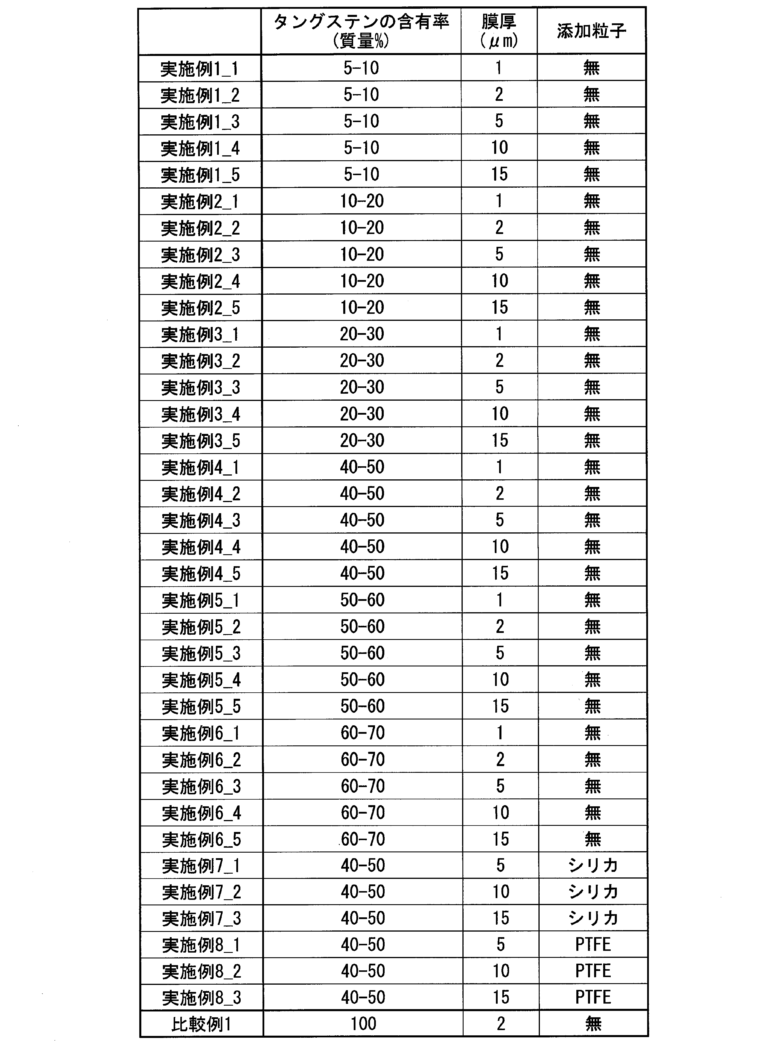
[実施例1_1~5]
実施例1_1~5は、上述の第1の実施形態の電極部101Aに対応する実施例とされた。
実施例1_1では、電極基材1の材質としてはステンレス鋼であるSUS304が用いられた。電極基材1の突出部101aの外形は、外径0.8mmの円柱とされた。
皮膜2Aは、第1金属と第2金属とのみで形成された。皮膜2Aには、粒子は含まれなかった。皮膜2Aの第1金属はタングステン(W)が用いられた。皮膜2Aの第2金属としてはニッケル(Ni)が用いられた。
[表1]に示すように、皮膜2AにおけるWの含有率は、5質量%以上10質量%未満とされた。ここで、含有率の数値を明示していないのは、複数の供試サンプル間で製法上および測定上の理由で含有率の数値がばらついたためである。
皮膜2Aの厚さ([表1]では「膜厚」と記載)は1μmとされた。
このような構成の実施例1_1の皮膜2Aは、電解メッキによって形成された。メッキ浴には、硫酸ニッケルおよびタングステン酸ナトリウムが添加された。硫酸ニッケルおよびタングステン酸ナトリウムに対するタングステン酸ナトリウムの比率は、5mol%とされた。
電極基材1を陰極として、上述のメッキ浴中で電解メッキが行われた。通電時間および電流量を調整することによって、電極基材1の基材表面1a上に1μmのNi-W膜が形成された。
形成されたNi-W膜に対して、EDX分析(エネルギー分散型X線分析、Energy Dispersive X-ray spectrometry)を行ったところ、皮膜2AにおけるWの含有率は、5質量%以上10質量%未満になっていた。
実施例1_1~5は、上述の第1の実施形態の電極部101Aに対応する実施例とされた。
実施例1_1では、電極基材1の材質としてはステンレス鋼であるSUS304が用いられた。電極基材1の突出部101aの外形は、外径0.8mmの円柱とされた。
皮膜2Aは、第1金属と第2金属とのみで形成された。皮膜2Aには、粒子は含まれなかった。皮膜2Aの第1金属はタングステン(W)が用いられた。皮膜2Aの第2金属としてはニッケル(Ni)が用いられた。
[表1]に示すように、皮膜2AにおけるWの含有率は、5質量%以上10質量%未満とされた。ここで、含有率の数値を明示していないのは、複数の供試サンプル間で製法上および測定上の理由で含有率の数値がばらついたためである。
皮膜2Aの厚さ([表1]では「膜厚」と記載)は1μmとされた。
このような構成の実施例1_1の皮膜2Aは、電解メッキによって形成された。メッキ浴には、硫酸ニッケルおよびタングステン酸ナトリウムが添加された。硫酸ニッケルおよびタングステン酸ナトリウムに対するタングステン酸ナトリウムの比率は、5mol%とされた。
電極基材1を陰極として、上述のメッキ浴中で電解メッキが行われた。通電時間および電流量を調整することによって、電極基材1の基材表面1a上に1μmのNi-W膜が形成された。
形成されたNi-W膜に対して、EDX分析(エネルギー分散型X線分析、Energy Dispersive X-ray spectrometry)を行ったところ、皮膜2AにおけるWの含有率は、5質量%以上10質量%未満になっていた。
実施例1_2の電極部101Aは、皮膜2Aの厚さが2μmとされた以外は、実施例1_1と同様に形成された。
実施例1_3の電極部101Aは、皮膜2Aの厚さが5μmとされた以外は、実施例1_1と同様に形成された。
実施例1_4の電極部101Aは、皮膜2Aの厚さが10μmとされた以外は、実施例1_1と同様に形成された。
実施例1_5の電極部101Aは、皮膜2Aの厚さが15μmとされた以外は、実施例1_1と同様に形成された。
実施例1_2~5におけるNi-W膜に対して、EDX分析を行ったところ、各皮膜2AにおけるWの含有率は、膜厚等によるばらつきはあったが、いずれも5質量%以上10質量%未満になっていた。
実施例1_3の電極部101Aは、皮膜2Aの厚さが5μmとされた以外は、実施例1_1と同様に形成された。
実施例1_4の電極部101Aは、皮膜2Aの厚さが10μmとされた以外は、実施例1_1と同様に形成された。
実施例1_5の電極部101Aは、皮膜2Aの厚さが15μmとされた以外は、実施例1_1と同様に形成された。
実施例1_2~5におけるNi-W膜に対して、EDX分析を行ったところ、各皮膜2AにおけるWの含有率は、膜厚等によるばらつきはあったが、いずれも5質量%以上10質量%未満になっていた。
[実施例2_1~実施例6_5]
実施例2_1~実施例6_5は、上述の第1の実施形態の電極部101Aに対応する実施例とされた。
実施例2_1~5の電極部101Aは、皮膜2AにおけるWの含有率が10質量%以20質量%未満になっていた以外は、実施例1_1~5と同様に形成された。このようなWの含有率は、メッキ浴におけるタングステン酸ナトリウムの比率が、10mol%とされることによって得られた。
実施例3_1~5の電極部101Aは、皮膜2AにおけるWの含有率が20質量%以30質量%未満になっていた以外は、実施例1_1~5と同様に形成された。このようなWの含有率は、メッキ浴におけるタングステン酸ナトリウムの比率が、20mol%とされることによって得られた。
実施例4_1~5の電極部101Aは、皮膜2AにおけるWの含有率が40質量%以50質量%未満になっていた以外は、実施例1_1~5と同様に形成された。このようなWの含有率は、メッキ浴におけるタングステン酸ナトリウムの比率が、40mol%とされることによって得られた。
実施例5_1~5の電極部101Aは、皮膜2AにおけるWの含有率が50質量%以60質量%未満になっていた以外は、実施例1_1~5と同様に形成された。このようなWの含有率は、メッキ浴におけるタングステン酸ナトリウムの比率が、50mol%とされることによって得られた。
実施例6_1~5の電極部101Aは、皮膜2AにおけるWの含有率が60質量%以70質量%未満になっていた以外は、実施例1_1~5と同様に形成された。このようなWの含有率は、メッキ浴におけるタングステン酸ナトリウムの比率が、60mol%とされることによって得られた。
実施例2_1~実施例6_5は、上述の第1の実施形態の電極部101Aに対応する実施例とされた。
実施例2_1~5の電極部101Aは、皮膜2AにおけるWの含有率が10質量%以20質量%未満になっていた以外は、実施例1_1~5と同様に形成された。このようなWの含有率は、メッキ浴におけるタングステン酸ナトリウムの比率が、10mol%とされることによって得られた。
実施例3_1~5の電極部101Aは、皮膜2AにおけるWの含有率が20質量%以30質量%未満になっていた以外は、実施例1_1~5と同様に形成された。このようなWの含有率は、メッキ浴におけるタングステン酸ナトリウムの比率が、20mol%とされることによって得られた。
実施例4_1~5の電極部101Aは、皮膜2AにおけるWの含有率が40質量%以50質量%未満になっていた以外は、実施例1_1~5と同様に形成された。このようなWの含有率は、メッキ浴におけるタングステン酸ナトリウムの比率が、40mol%とされることによって得られた。
実施例5_1~5の電極部101Aは、皮膜2AにおけるWの含有率が50質量%以60質量%未満になっていた以外は、実施例1_1~5と同様に形成された。このようなWの含有率は、メッキ浴におけるタングステン酸ナトリウムの比率が、50mol%とされることによって得られた。
実施例6_1~5の電極部101Aは、皮膜2AにおけるWの含有率が60質量%以70質量%未満になっていた以外は、実施例1_1~5と同様に形成された。このようなWの含有率は、メッキ浴におけるタングステン酸ナトリウムの比率が、60mol%とされることによって得られた。
[実施例7_1~3]
実施例7_1~3は、上述の第2の実施形態の電極部101Bに対応する実施例とされた。
実施例7_1は、上述の第2の実施形態の電極部101Bに対応する実施例とされた。
電極基材1は、実施例1_1と同様に形成された。
皮膜2Bの金属膜21は、WとNiとで構成された。皮膜2BにおけるWの含有率は、実施例4-3と同様、40質量%以上50質量%以下とされた。
皮膜2Bに含有された非粘着性粒子22([表1]では「添加粒子」と記載)としては、メチル基修飾シリカ粒子([表1]では「シリカ」と記載)が用いられた。具体的には、平均粒子径1μmのトリメチルシリル修飾タイプのsicastar(登録商標)(商品名;Micromod社製)が用いられた。
皮膜2Bにおける非粘着性粒子22の含有率は、3vol%とされた。
皮膜2Bの厚さは、実施例4_3と同様、5μmとされた。
このような皮膜2Bは、メッキ浴に非粘着性粒子22を分散された以外は、実施例4-3と同様の電解メッキによって形成された。
実施例7_1~3は、上述の第2の実施形態の電極部101Bに対応する実施例とされた。
実施例7_1は、上述の第2の実施形態の電極部101Bに対応する実施例とされた。
電極基材1は、実施例1_1と同様に形成された。
皮膜2Bの金属膜21は、WとNiとで構成された。皮膜2BにおけるWの含有率は、実施例4-3と同様、40質量%以上50質量%以下とされた。
皮膜2Bに含有された非粘着性粒子22([表1]では「添加粒子」と記載)としては、メチル基修飾シリカ粒子([表1]では「シリカ」と記載)が用いられた。具体的には、平均粒子径1μmのトリメチルシリル修飾タイプのsicastar(登録商標)(商品名;Micromod社製)が用いられた。
皮膜2Bにおける非粘着性粒子22の含有率は、3vol%とされた。
皮膜2Bの厚さは、実施例4_3と同様、5μmとされた。
このような皮膜2Bは、メッキ浴に非粘着性粒子22を分散された以外は、実施例4-3と同様の電解メッキによって形成された。
実施例7_2の電極部101Bは、皮膜2Bの厚さが10μmとされた以外は、実施例7_1と同様に形成された。
実施例7_3の電極部101Bは、皮膜2Bの厚さが15μmとされた以外は、実施例7_1と同様に形成された。
実施例7_3の電極部101Bは、皮膜2Bの厚さが15μmとされた以外は、実施例7_1と同様に形成された。
[実施例8_1~3]
実施例8_1~3は、実施例7_1~3と同様、上述の第2の実施形態の電極部101Bに対応する実施例とされた。
実施例8_1~3の電極部101Bは、非粘着性粒子22として、平均粒子径1μmのPTFE粒子([表1]では「PTFE」と記載)が用いられた以外は、それぞれ、実施例7_1~3と同様に形成された。
実施例8_1~3は、実施例7_1~3と同様、上述の第2の実施形態の電極部101Bに対応する実施例とされた。
実施例8_1~3の電極部101Bは、非粘着性粒子22として、平均粒子径1μmのPTFE粒子([表1]では「PTFE」と記載)が用いられた以外は、それぞれ、実施例7_1~3と同様に形成された。
[比較例1]
比較例1は、皮膜におけるWの比率が100%とされた以外は、実施例1_3と同様に構成された。比較例1の皮膜の厚さは2μmとされた。
ただし、比較例1の皮膜は、スパッタリングによって形成された。
比較例1は、皮膜におけるWの比率が100%とされた以外は、実施例1_3と同様に構成された。比較例1の皮膜の厚さは2μmとされた。
ただし、比較例1の皮膜は、スパッタリングによって形成された。
[評価]
各実施例、比較例の各電極部は、高周波処置具100に取り付けられた後、高周波処置具100を用いた評価試験が行われた。評価試験としては、凝固モード試験、切開モード試験、および貼り付き評価試験が行われた。
各実施例、比較例の各電極部は、高周波処置具100に取り付けられた後、高周波処置具100を用いた評価試験が行われた。評価試験としては、凝固モード試験、切開モード試験、および貼り付き評価試験が行われた。
[凝固モード試験および切開モード試験]
凝固モード試験および切開モード試験では、実施例1_1~実施例6_5および比較例1の各電極部によって、豚胃粘膜(生体組織)を被検体として、組織焼灼が行われた。
凝固モード試験では、高周波処置具100の電源条件が凝固モードに設定された。凝固モード試験では、電極部による生体組織の凝固処置が凝固モードによる1秒の通電で行われた。1回の通電の後、通電は0.5秒間、休止された。このような凝固処置を、60回繰り返す動作が1サイクルと定義された。凝固モード試験では、電極部への生体組織の貼り付きによって生体組織の除去が必要となるまで、試験が続行された。
切開モード試験では、高周波処置具100の電源条件が切開モードに設定された。切開モード試験では、電極部による生体組織の切開処置が切開モードによる0.5秒の通電で行われた。1回の通電の後、通電は0.5秒間、休止された。このような切開処置を、60回繰り返す動作が1サイクルと定義された。切開モード試験では、電極部への生体組織の貼り付きによって生体組織の除去が必要となるまで、試験が続行された。
凝固モード試験および切開モード試験では、いずれも続行されたサイクル数によって電極部の耐久性が評価された。
さらに、各試験の後、電極部に付着した組織が除去され、電極部の表面のSEM観察およびEDX分析が行われた。
凝固モード試験および切開モード試験では、実施例1_1~実施例6_5および比較例1の各電極部によって、豚胃粘膜(生体組織)を被検体として、組織焼灼が行われた。
凝固モード試験では、高周波処置具100の電源条件が凝固モードに設定された。凝固モード試験では、電極部による生体組織の凝固処置が凝固モードによる1秒の通電で行われた。1回の通電の後、通電は0.5秒間、休止された。このような凝固処置を、60回繰り返す動作が1サイクルと定義された。凝固モード試験では、電極部への生体組織の貼り付きによって生体組織の除去が必要となるまで、試験が続行された。
切開モード試験では、高周波処置具100の電源条件が切開モードに設定された。切開モード試験では、電極部による生体組織の切開処置が切開モードによる0.5秒の通電で行われた。1回の通電の後、通電は0.5秒間、休止された。このような切開処置を、60回繰り返す動作が1サイクルと定義された。切開モード試験では、電極部への生体組織の貼り付きによって生体組織の除去が必要となるまで、試験が続行された。
凝固モード試験および切開モード試験では、いずれも続行されたサイクル数によって電極部の耐久性が評価された。
さらに、各試験の後、電極部に付着した組織が除去され、電極部の表面のSEM観察およびEDX分析が行われた。
[貼り付き評価試験]
貼り付き評価試験では、実施例4_3~5、実施例7_1~3、実施例8_1~3の各電極部によって、1サイクルの凝固モード試験が行われた。試験後、目視で、各電極表面が観察された。
貼り付き評価試験では、実施例4_3~5、実施例7_1~3、実施例8_1~3の各電極部によって、1サイクルの凝固モード試験が行われた。試験後、目視で、各電極表面が観察された。
[評価結果1]
下記[表2]に凝固モード試験の評価結果(評価結果1)を示した。
下記[表2]に凝固モード試験の評価結果(評価結果1)を示した。
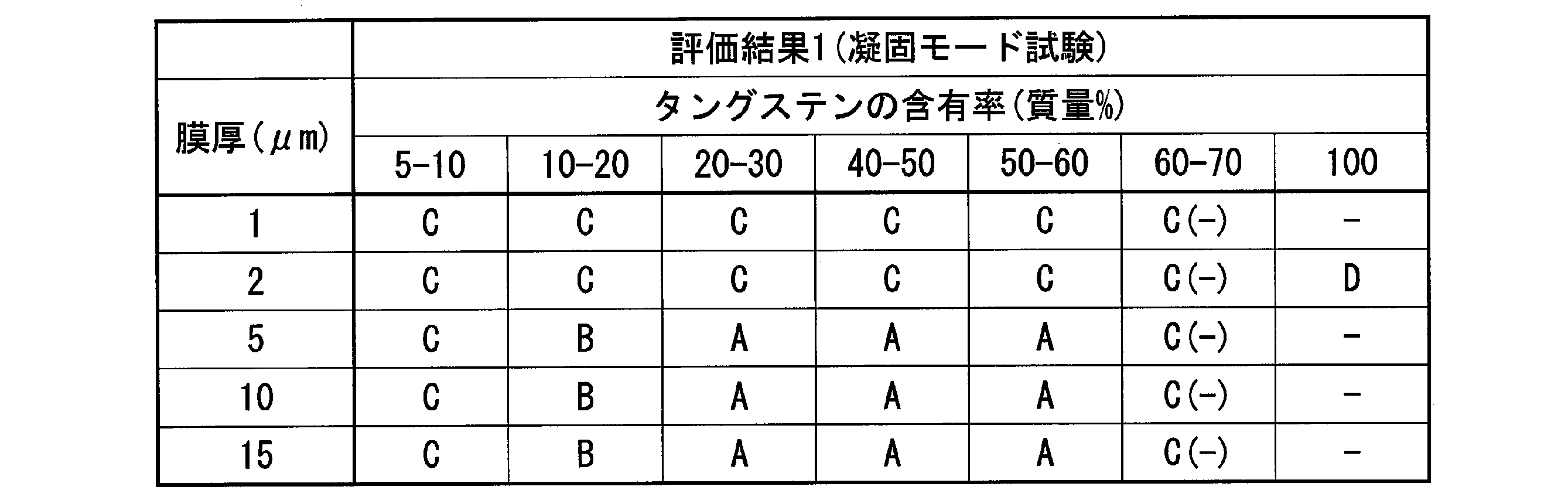
[表2]では、各行に皮膜の厚さ([表2]には「膜厚」と記載)、各列にWの含有率を取り、各実施例および比較例1の評価結果を示した。[表2]における含有率の記載において、例えば、「5-10」は、「5質量%以上10質量%未満」を表す。
例えば、「5-10」列と「1」行とが交差する欄には、実施例1_1の評価結果「C」が記載されている。例えば、「100」列と「2」行とが交差する欄には、比較例1の評価結果「D」が記載されている。
同様に、「10-20」列、「20-30」列、「40-50」列、「60-70」列には、それぞれ、実施例2_1~5、実施例3_1~5、実施例4_1~5、実施例5_1~5、実施例6_1~4の各評価結果が記載されている。
例えば、「5-10」列と「1」行とが交差する欄には、実施例1_1の評価結果「C」が記載されている。例えば、「100」列と「2」行とが交差する欄には、比較例1の評価結果「D」が記載されている。
同様に、「10-20」列、「20-30」列、「40-50」列、「60-70」列には、それぞれ、実施例2_1~5、実施例3_1~5、実施例4_1~5、実施例5_1~5、実施例6_1~4の各評価結果が記載されている。
評価は、「非常に良い」(very good、[表2]では「A」)、「良い」(good、[表2]では「B」)、「可」(fair、[表2]では「C」)、「不良」(no good、[表2]では「D」)の四段階でなされた。
試験が2サイクルを超えて続行された場合の評価は「非常に良い」と定義した。
試験が1サイクルを超えて続行され、2サイクル目を終了できなかった場合の評価は「良い」と定義した。
試験が1サイクル目の30回以上60回以下で終了した場合の評価は「可」と定義した。
試験が1サイクル目の29回以下で終了した場合の評価は「不良」と定義した。
試験が2サイクルを超えて続行された場合の評価は「非常に良い」と定義した。
試験が1サイクルを超えて続行され、2サイクル目を終了できなかった場合の評価は「良い」と定義した。
試験が1サイクル目の30回以上60回以下で終了した場合の評価は「可」と定義した。
試験が1サイクル目の29回以下で終了した場合の評価は「不良」と定義した。
図6は、実施例の医療機器用電極の表面のSEM画像である。図7は、比較例の医療機器用電極の表面のSEM画像である。
[表2]に示すように、凝固モード試験では、実施例3_3~5、実施例4_3~5、実施例5_3~5、実施例6_3~5の評価は「非常に良い」であった。実施例2_3~5の評価は「良い」であった。
図6に示したのは、生体組織除去後の実施例の電極表面のSEM画像の一例である。図6から分かるように、実施例の電極表面における皮膜には、割れ、はがれは生じていなかった。
[表2]に示すように、凝固モード試験では、実施例3_3~5、実施例4_3~5、実施例5_3~5、実施例6_3~5の評価は「非常に良い」であった。実施例2_3~5の評価は「良い」であった。
図6に示したのは、生体組織除去後の実施例の電極表面のSEM画像の一例である。図6から分かるように、実施例の電極表面における皮膜には、割れ、はがれは生じていなかった。
実施例1_1~5、実施例2_1~2、実施例3_1~2、実施例4_1~2、実施例5_1~2(以下、まとめて、実施例群Xと略記)の評価は「可」であった。
ただし、実施例群Xでは、生体組織を除去すれば、再使用が可能なレベルであった。
実施例群Xの電極表面をSEM観察したところ、皮膜が薄くなっていることが分かった。一部には電極表面が露出している箇所も見られた。
実施例6_1~5の評価は上記の評価基準では「可」であった。しかし、実施例6_1~5の各電極表面をSEM観察したところ、一部に皮膜のはがれが観察された。生体組織を除去して再使用しても、早期に生体組織の除去が必要になる点では、「可」であっても、実施例群Xに比べるとやや劣る状態であった。そこで、[表2]には「C(-)」と記載した。
ただし、実施例群Xでは、生体組織を除去すれば、再使用が可能なレベルであった。
実施例群Xの電極表面をSEM観察したところ、皮膜が薄くなっていることが分かった。一部には電極表面が露出している箇所も見られた。
実施例6_1~5の評価は上記の評価基準では「可」であった。しかし、実施例6_1~5の各電極表面をSEM観察したところ、一部に皮膜のはがれが観察された。生体組織を除去して再使用しても、早期に生体組織の除去が必要になる点では、「可」であっても、実施例群Xに比べるとやや劣る状態であった。そこで、[表2]には「C(-)」と記載した。
これに対して、比較例1の評価は「不可」であった。
図7に示したのは、生体組織除去後の比較例1の電極表面のSEM画像である。図7から分かるように、比較例1の電極表面には、Wからなる皮膜が剥離した剥離片(符号Bで示す)が見られ、基材表面(符号Cで示す)が露出していた。
図7に示したのは、生体組織除去後の比較例1の電極表面のSEM画像である。図7から分かるように、比較例1の電極表面には、Wからなる皮膜が剥離した剥離片(符号Bで示す)が見られ、基材表面(符号Cで示す)が露出していた。
評価結果1によれば、Wの含有率が20質量%以上60質量%未満であって、皮膜の厚さが5μm以上の場合に特に良好な結果が得られた。
Wの含有率が10質量%未満では、電極表面において融点の低いNiが占める面積が大きすぎたことが原因で、皮膜の消耗が激しかったと考えられる。
Wの含有率が10質量%未満では、電極表面において融点の低いNiが占める面積が大きすぎたことが原因で、皮膜の消耗が激しかったと考えられる。
[評価結果2]
下記[表3]に切開モード試験の評価結果(評価結果2)を示した。
下記[表3]に切開モード試験の評価結果(評価結果2)を示した。
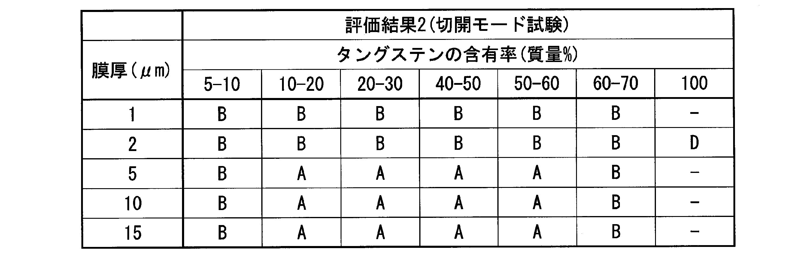
[表3]における行、列と各実施例、比較例1との対応関係および各評価の定義は、[表2]と同様とされた。
[表3]に示したように、切開モード試験では、実施例2_3~5、実施例3_3~5、実施例4_3~5、実施例5_3~5、実施例6_3~5の評価は「非常に良い」であった。その他の実施例の評価は「良い」であった。凝固モード試験で「可」もしくは「良い」と評価された各実施例は、それぞれ「良い」、「非常に良い」という評価が得られた。
切開モードでは電極部が移動する結果、凝固モードに比べると、焼灼が進んだ生体組織が電極表面にとどまる時間が短くなる。この結果、スパークの発生が少なかったと考えられる。
[表3]に示したように、切開モード試験では、実施例2_3~5、実施例3_3~5、実施例4_3~5、実施例5_3~5、実施例6_3~5の評価は「非常に良い」であった。その他の実施例の評価は「良い」であった。凝固モード試験で「可」もしくは「良い」と評価された各実施例は、それぞれ「良い」、「非常に良い」という評価が得られた。
切開モードでは電極部が移動する結果、凝固モードに比べると、焼灼が進んだ生体組織が電極表面にとどまる時間が短くなる。この結果、スパークの発生が少なかったと考えられる。
これに対して、比較例1の評価は、凝固モード試験と同様、「不可」であった。
比較例1の電極部では、切開モードにおいても、皮膜の消耗およびはがれが激しかったことが原因で、各実施例に比べて生体組織の付着が起こりやすかったと考えられる。
比較例1の電極部では、切開モードにおいても、皮膜の消耗およびはがれが激しかったことが原因で、各実施例に比べて生体組織の付着が起こりやすかったと考えられる。
[評価結果3]
下記[表4]に、貼り付き評価試験における実施例4_3~5、実施例7_1~3、実施例8_1~3の評価結果(評価結果3)を示した。
下記[表4]に、貼り付き評価試験における実施例4_3~5、実施例7_1~3、実施例8_1~3の評価結果(評価結果3)を示した。
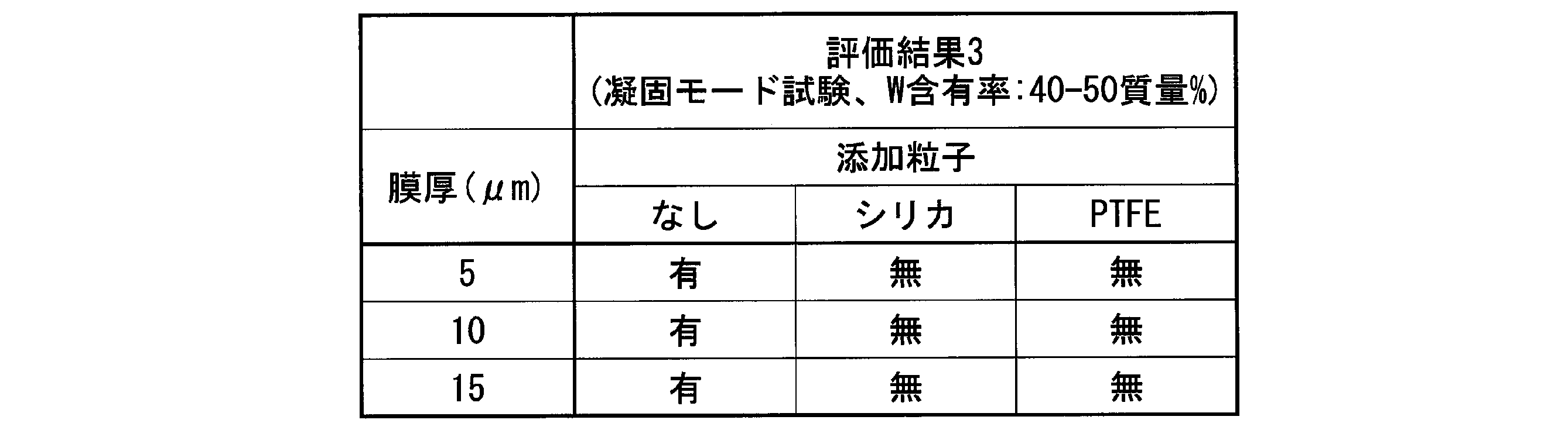
[表4]において「なし」列には、実施例4_3~5の評価結果が示された。「シリカ」列には、実施例7_1~3の評価結果が示された。「PTFE」列には、実施例8_1~3の評価結果が示された。
[表4]における各評価結果は、生体組織の付着の有無で記載された。「有」は、目視によって生体組織の付着が観察されたことを表している。「無」は、目視によって生体組織の付着が観察されなかったことを表している。
[表4]に示したように、非粘着性粒子22が含有されなかった実施例4_3~5では、いずれも生体組織が付着していた。ただし、付着量は、通電には支障がない程度であった。このように付着量が少なかったので、上述の凝固モード試験では、生体組織を除去することなく2サイクル目の試験を続行することができた。
これに対して、実施例7_1~3、実施例8_1~3では、目視では、生体組織の付着が認められなかった。
このように、実施例7_1~3、実施例8_1~3では、電極表面に非粘着性粒子22が露出していた結果、金属膜21の構成が実施例4_3~5の皮膜2Aと同等であっても。生体組織の付着がさらに抑制されていたと考えられる。
[表4]における各評価結果は、生体組織の付着の有無で記載された。「有」は、目視によって生体組織の付着が観察されたことを表している。「無」は、目視によって生体組織の付着が観察されなかったことを表している。
[表4]に示したように、非粘着性粒子22が含有されなかった実施例4_3~5では、いずれも生体組織が付着していた。ただし、付着量は、通電には支障がない程度であった。このように付着量が少なかったので、上述の凝固モード試験では、生体組織を除去することなく2サイクル目の試験を続行することができた。
これに対して、実施例7_1~3、実施例8_1~3では、目視では、生体組織の付着が認められなかった。
このように、実施例7_1~3、実施例8_1~3では、電極表面に非粘着性粒子22が露出していた結果、金属膜21の構成が実施例4_3~5の皮膜2Aと同等であっても。生体組織の付着がさらに抑制されていたと考えられる。
以上、本発明の好ましい各実施形態を各実施例とともに説明したが、本発明はこれらの各実施形態、各実施例に限定されることはない。本発明の趣旨を逸脱しない範囲で、構成の付加、省略、置換、およびその他の変更が可能である。
また、本発明は前述した説明によって限定されることはなく、添付の特許請求の範囲によってのみ限定される。
例えば、第3~第5の実施形態における各皮膜において、第2の実施形態における非粘着性粒子22が含まれてもよい。
例えば、第1、第2、第4、および第5の実施形態における各皮膜と電極基材1との間に、第3の実施形態における第2金属層32が設けられていてもよい。
例えば、第2、第3、および第5の実施形態における各皮膜と電極基材との間に、第4の実施形態における中間層42が設けられてもよい。
また、本発明は前述した説明によって限定されることはなく、添付の特許請求の範囲によってのみ限定される。
例えば、第3~第5の実施形態における各皮膜において、第2の実施形態における非粘着性粒子22が含まれてもよい。
例えば、第1、第2、第4、および第5の実施形態における各皮膜と電極基材1との間に、第3の実施形態における第2金属層32が設けられていてもよい。
例えば、第2、第3、および第5の実施形態における各皮膜と電極基材との間に、第4の実施形態における中間層42が設けられてもよい。
上記実施形態によれば、良好な処置性能を長期間維持することができる高周波処置に用いられる医療機器用電極および医療機器を提供できる。
1 電極基材(基材)
1a 基材表面(基材の表面)
2A、2B、2C、2D、2E 皮膜
21 金属膜
22 非粘着性粒子
31 第1金属層
32 第2金属層
41 最表層
42 中間層
100 高周波処置具(医療機器)
101a 突出部
101A、101B、101C、101D、101B電極部(医療機器用電極)
1a 基材表面(基材の表面)
2A、2B、2C、2D、2E 皮膜
21 金属膜
22 非粘着性粒子
31 第1金属層
32 第2金属層
41 最表層
42 中間層
100 高周波処置具(医療機器)
101a 突出部
101A、101B、101C、101D、101B電極部(医療機器用電極)
Claims (6)
- 金属製の基材と、
前記基材の表面に形成された皮膜と、
を備え、
前記皮膜は、第1金属と第2金属とを含んでおり、
前記第1金属は、タングステン、タンタル、ニオブ、およびモリブデンからなる群から選ばれた1以上の金属を含み、
前記第2金属は、ニッケル、チタン、およびアルミニウムからなる群から選ばれた1以上の金属を含む、
高周波処置に用いられる医療機器用電極。 - 前記皮膜の厚さは、
5μm以上50μm以下である、
請求項1に記載の高周波処置に用いられる医療機器用電極。 - 前記皮膜における前記第1金属の含有率は、
20質量%以上50質量%以下である、
請求項1に記載の高周波処置に用いられる医療機器用電極。 - 前記皮膜の表面には、非粘着性粒子が分散されており、
前記非粘着性粒子は、PTFE粒子およびメチル基で化学修飾されたシリカ粒子の少なくとも一方を含む、
請求項1に記載の高周波処置に用いられる医療機器用電極。 - 前記皮膜は、
前記第1金属および前記第2金属を含むメッキ膜からなる、請求項1に記載の高周波処置に用いられる医療機器用電極。 - 請求項1に記載の高周波処置に用いられる医療機器用電極を備える、医療機器。
Applications Claiming Priority (2)
| Application Number | Priority Date | Filing Date | Title |
|---|---|---|---|
| JP2018-197008 | 2018-10-18 | ||
| JP2018197008A JP7179575B2 (ja) | 2018-10-18 | 2018-10-18 | 高周波処置に用いられる医療機器用電極および医療機器 |
Publications (1)
| Publication Number | Publication Date |
|---|---|
| WO2020079947A1 true WO2020079947A1 (ja) | 2020-04-23 |
Family
ID=70283956
Family Applications (1)
| Application Number | Title | Priority Date | Filing Date |
|---|---|---|---|
| PCT/JP2019/032544 Ceased WO2020079947A1 (ja) | 2018-10-18 | 2019-08-21 | 高周波処置に用いられる医療機器用電極および医療機器 |
Country Status (2)
| Country | Link |
|---|---|
| JP (1) | JP7179575B2 (ja) |
| WO (1) | WO2020079947A1 (ja) |
Families Citing this family (3)
| Publication number | Priority date | Publication date | Assignee | Title |
|---|---|---|---|---|
| KR102642223B1 (ko) * | 2021-05-21 | 2024-02-28 | 최인상 | 전기수술 핸드피이스용 전도성 전극 |
| US20240081889A1 (en) * | 2020-12-31 | 2024-03-14 | In-sang Choi | Conductive electrode for electrosurgical handpiece and manufacturing method therefor |
| DE102023123253A1 (de) * | 2023-08-29 | 2025-03-06 | Olympus Winter & Ibe Gmbh | Elektrode für ein elektrochirurgisches Handinstrument |
Citations (4)
| Publication number | Priority date | Publication date | Assignee | Title |
|---|---|---|---|---|
| JPH10277050A (ja) * | 1997-04-04 | 1998-10-20 | Olympus Optical Co Ltd | 内視鏡用高周波処置具 |
| JP2006288425A (ja) * | 2005-04-05 | 2006-10-26 | Johnson & Johnson Kk | バイポーラピンセット |
| JP2007510519A (ja) * | 2003-11-10 | 2007-04-26 | チーム メディカル エル.エル.シー. | 電気手術器具 |
| JP2011505198A (ja) * | 2007-11-30 | 2011-02-24 | エシコン・エンド−サージェリィ・インコーポレイテッド | 超音波手術刃 |
Family Cites Families (1)
| Publication number | Priority date | Publication date | Assignee | Title |
|---|---|---|---|---|
| JP3891411B2 (ja) * | 2002-04-18 | 2007-03-14 | 日立金属株式会社 | 超硬合金製圧延用複合ロール |
-
2018
- 2018-10-18 JP JP2018197008A patent/JP7179575B2/ja active Active
-
2019
- 2019-08-21 WO PCT/JP2019/032544 patent/WO2020079947A1/ja not_active Ceased
Patent Citations (4)
| Publication number | Priority date | Publication date | Assignee | Title |
|---|---|---|---|---|
| JPH10277050A (ja) * | 1997-04-04 | 1998-10-20 | Olympus Optical Co Ltd | 内視鏡用高周波処置具 |
| JP2007510519A (ja) * | 2003-11-10 | 2007-04-26 | チーム メディカル エル.エル.シー. | 電気手術器具 |
| JP2006288425A (ja) * | 2005-04-05 | 2006-10-26 | Johnson & Johnson Kk | バイポーラピンセット |
| JP2011505198A (ja) * | 2007-11-30 | 2011-02-24 | エシコン・エンド−サージェリィ・インコーポレイテッド | 超音波手術刃 |
Also Published As
| Publication number | Publication date |
|---|---|
| JP7179575B2 (ja) | 2022-11-29 |
| JP2020062297A (ja) | 2020-04-23 |
Similar Documents
| Publication | Publication Date | Title |
|---|---|---|
| JP4391440B2 (ja) | バイポーラピンセット | |
| US6749610B2 (en) | Electro-surgical forceps having fully plated tines and process for manufacturing same | |
| WO2020079947A1 (ja) | 高周波処置に用いられる医療機器用電極および医療機器 | |
| US8656585B2 (en) | Process for manufacturing electrosurgical forceps with composite material tips | |
| JP5667350B2 (ja) | コンタクトプローブピン | |
| JP6804931B2 (ja) | 医療機器用付着防止膜および医療機器 | |
| CN114126523A (zh) | 电极装置 | |
| US20070208341A1 (en) | Electro-surgical forceps having fully copper-plated tines and process for manufacturing same | |
| US20190192212A1 (en) | Conductive adhesion preventing film for medical use and medical device | |
| JP2010284439A (ja) | 医療機器用電極および医療用処置具 | |
| JP6865666B2 (ja) | 高周波医療機器用の電極および高周波医療機器 | |
| CN105164304B (zh) | 用于电外科器械的含ZrO2的涂层体系 | |
| JP2010227462A (ja) | 医療機器用電極および医療用処置具 | |
| JP2019076218A (ja) | 高周波医療機器用の電極および高周波医療機器 | |
| CN110495948B (zh) | 医用双极电凝镊及其制造方法 | |
| JP6856492B2 (ja) | 高周波医療機器用の電極および高周波医療機器 | |
| TW201217792A (en) | Probe pin for semiconductor inspection devices, method for producing same, and semiconductor inspection method | |
| JP2011024871A (ja) | 医療機器用処置部、医療機器および医療機器用処置部の製造方法 | |
| JP2010227365A (ja) | 医療機器用電極および医療用処置具 | |
| JP2017159002A (ja) | 医療用処置具 | |
| JP6027857B2 (ja) | フッ素樹脂製部品の製造方法およびフッ素樹脂製部品 | |
| TW202137943A (zh) | 電外科用電極 | |
| CN117157027A (zh) | 高频医疗设备用电极和医疗设备 | |
| WO2018190000A1 (ja) | 医療機器用高周波電極および医療機器 |
Legal Events
| Date | Code | Title | Description |
|---|---|---|---|
| 121 | Ep: the epo has been informed by wipo that ep was designated in this application |
Ref document number: 19874138 Country of ref document: EP Kind code of ref document: A1 |
|
| NENP | Non-entry into the national phase |
Ref country code: DE |
|
| 122 | Ep: pct application non-entry in european phase |
Ref document number: 19874138 Country of ref document: EP Kind code of ref document: A1 |