WO2020075552A1 - スイッチトキャパシタアンプおよびad変換装置 - Google Patents
スイッチトキャパシタアンプおよびad変換装置 Download PDFInfo
- Publication number
- WO2020075552A1 WO2020075552A1 PCT/JP2019/038501 JP2019038501W WO2020075552A1 WO 2020075552 A1 WO2020075552 A1 WO 2020075552A1 JP 2019038501 W JP2019038501 W JP 2019038501W WO 2020075552 A1 WO2020075552 A1 WO 2020075552A1
- Authority
- WO
- WIPO (PCT)
- Prior art keywords
- feedback
- amplifier
- sampling
- capacitance
- operational amplifier
- Prior art date
- Legal status (The legal status is an assumption and is not a legal conclusion. Google has not performed a legal analysis and makes no representation as to the accuracy of the status listed.)
- Ceased
Links
Images










Classifications
-
- H—ELECTRICITY
- H03—ELECTRONIC CIRCUITRY
- H03F—AMPLIFIERS
- H03F3/00—Amplifiers with only discharge tubes or only semiconductor devices as amplifying elements
- H03F3/34—DC amplifiers in which all stages are DC-coupled
-
- H—ELECTRICITY
- H03—ELECTRONIC CIRCUITRY
- H03F—AMPLIFIERS
- H03F3/00—Amplifiers with only discharge tubes or only semiconductor devices as amplifying elements
- H03F3/70—Charge amplifiers
-
- H—ELECTRICITY
- H03—ELECTRONIC CIRCUITRY
- H03M—CODING; DECODING; CODE CONVERSION IN GENERAL
- H03M1/00—Analogue/digital conversion; Digital/analogue conversion
- H03M1/06—Continuously compensating for, or preventing, undesired influence of physical parameters
- H03M1/08—Continuously compensating for, or preventing, undesired influence of physical parameters of noise
-
- H—ELECTRICITY
- H03—ELECTRONIC CIRCUITRY
- H03M—CODING; DECODING; CODE CONVERSION IN GENERAL
- H03M1/00—Analogue/digital conversion; Digital/analogue conversion
- H03M1/12—Analogue/digital converters
-
- H—ELECTRICITY
- H03—ELECTRONIC CIRCUITRY
- H03M—CODING; DECODING; CODE CONVERSION IN GENERAL
- H03M1/00—Analogue/digital conversion; Digital/analogue conversion
- H03M1/12—Analogue/digital converters
- H03M1/34—Analogue value compared with reference values
- H03M1/38—Analogue value compared with reference values sequentially only, e.g. successive approximation type
Definitions
- the present technology relates to a switched capacitor amplifier and an AD conversion device used for a proximity sensor or a displacement sensor.
- Sensors such as a proximity sensor and a displacement sensor detect an object or obtain a distance to the object by detecting a change in signal amplitude obtained by using magnetic induction or the like.
- a circuit for detecting the signal amplitude from the sensor there is, for example, a signal processing system using CDS (Correlated Double Sampling).
- CDS Correlated Double Sampling
- the CDS is generally used when detecting the difference due to the time change of one signal.
- CDS is a signal processing method adopted in, for example, an analog front end (AFE) for CCD.
- the signal processing method of the CDS has the merit that the difference between the output voltages before and after the sampling becomes the signal component as it is, so that the influence due to the individual variation of the signal source can be reduced and the low frequency noise can be suppressed.
- a general approach is to amplify a signal from a sensor with a preamplifier (PreAmp), perform differential signal processing with a CDS, and digitize it with an AD converter (ADC) (for example, , Patent Document 1).
- PreAmp preamplifier
- ADC AD converter
- the CDS and ADC have a large capacity (electrode area) ratio of the capacitor to the area (surface area) of the entire circuit due to the circuit configuration.
- kT / C noise k is Boltzmann's constant, T is absolute temperature, C is the capacitance of the capacitor
- an object of the present technology is to provide a switched capacitor amplifier and an AD conversion device that can reduce the area and power consumption of the entire circuit.
- a switched capacitor amplifier includes a plurality of sampling capacitors, a feedback capacitor, a switch group, and an operational amplifier.
- the plurality of sampling capacitors sample an analog signal.
- the feedback capacitors are capacitively arrayed.
- the switch group is connected to the feedback capacitor and has at least three connection destinations.
- the operational amplifier is subjected to negative feedback by one connection destination of the feedback capacitor and the switch group, and detects a difference in amplitude of the analog signal.
- the feedback capacitance may include a plurality of capacitive elements weighted by the power of 2 (n is an integer).
- the at least two connection destinations of the switch group may be a first reference potential and a second reference potential lower than the first reference potential, respectively.
- Another other connection destination of the switch group may be an output terminal of the operational amplifier.
- the switched capacitor amplifier may further include a controller.
- the controller is configured to be capable of generating a data signal for precharging the feedback capacitor with a level shift amount of electric charge corresponding to a predetermined amplitude value of the analog signal.
- the operational amplifier may have two states, a period for sampling the analog signal and a period for amplifying the sampled analog signal.
- the plurality of sampling capacitors have a capacitance for holding two analog signals having different time bases, and the operational amplifier has a difference between a holding voltage obtained in the first sampling and a holding voltage obtained in the second sampling. May be amplified at a capacity ratio with the feedback capacity.
- An AD conversion device includes a plurality of sampling capacitors, a feedback capacitor, a switch group, an operational amplifier, and a comparator.
- the plurality of sampling capacitors sample an analog signal.
- the feedback capacitors are capacitively arrayed.
- the operational amplifier is subjected to negative feedback by one connection destination of the feedback capacitor and the switch group, and detects a difference in amplitude of the analog signal.
- the comparator determines the magnitude relation of the difference between the output signals of the operational amplifier.
- the feedback capacitance may include a plurality of capacitive elements weighted by the power of 2 (n is an integer).
- At least two connection destinations of the switch group may be a high potential end and a low potential end of a reference voltage that defines the full scale of AD conversion.
- the other one connection destination of the switch group may be the input terminal of the operational amplifier.
- the AD converter may further include a controller.
- the controller includes a period for sampling the analog signal by the plurality of sampling capacitors, a period for amplifying the analog signal sampled by the ratio of the plurality of sampling capacitors and the feedback capacitor by the operational amplifier, and an amplified analog signal.
- the period for AD conversion is controlled based on the output of the comparator.
- the controller may be configured to control the feedback capacity in a binary search sequence according to the determination result of the comparator.
- the AD conversion device may further include a first switch connected between the input and output ends of the operational amplifier so as to be parallel to the switch group and the feedback capacitance.
- the AD converter may further include an auxiliary switch group.
- the auxiliary switch group is connected to the other end of the feedback capacitor and has two connection destinations, that is, a common potential and an output end of the operational amplifier.
- the controller is configured to set the connection destination of the auxiliary switch group to the common potential during the sampling period of the analog signal.
- the AD conversion device may further include a second switch and a third switch.
- the second switch is configured so that the other end of the feedback capacitor can be connected to the output end of the operational amplifier and a common potential.
- the third switch is configured to be able to connect the switch group to the input terminal of the operational amplifier and a common potential.
- the controller is configured to connect an input / output terminal of the operational amplifier to a common potential via the second switch and the third switch during a sampling period of the analog signal.
- An AD conversion device includes a plurality of sampling capacitors, a feedback capacitor, a comparator, and a switch group.
- the plurality of sampling capacitors sample an analog signal.
- the feedback capacitors are capacitively arrayed.
- the comparator determines the magnitude relationship of analog signals sampled by the sampling capacitor.
- the switch group is connected to the feedback capacitor and has at least three connection destinations, one of which is connectable to the input terminal of the comparator.
- the feedback capacitance may include a plurality of capacitive elements weighted by the power of 2 (n is an integer).
- At least two connection destinations of the switch group may be a high potential end and a low potential end of a reference voltage that defines the full scale of AD conversion.
- the AD converter may further include a controller.
- the controller controls a period during which the analog signal is sampled by the plurality of sampling capacitors and a period during which the sampled analog signal is AD-converted based on the output of the comparator.
- the controller is configured to connect the switch group to an input terminal of the comparator during a period in which the analog signal is sampled.
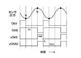
- FIG. 7 is a diagram showing an operation timing of the CDS amplifier of Comparative Example 1 described above.
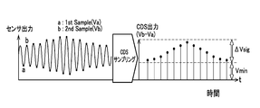
- 6 is a diagram showing an example of a signal amplitude detection image using the CDS amplifier of Comparative Example 1.
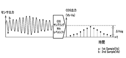
- FIG. It is a figure which shows an example of the signal amplitude detection image using the CDS amplifier which has a level shift function.
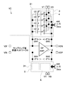
- composition of a CDS amplifier as a switched capacitor amplifier concerning a 1st embodiment of this art.
- FIG. 6 is a diagram showing an operation timing of the switched capacitor amplifier according to the first embodiment.
- FIG. 16 is a system diagram illustrating a method of estimating a level shift amount of a switched capacitor amplifier as a fourth embodiment of the present technology.
- 6 is a configuration example of a CDS amplifier and an ADC described as Comparative example 2 in the embodiment of the present technology.
- 7 is a diagram showing operation timings of a CDS amplifier and an ADC of Comparative Example 2.
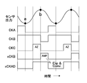
- FIG. It is a figure showing the composition of the AD converter concerning a 5th embodiment of this art. It is a figure which shows the operation timing of the AD converter which concerns on the said 5th Embodiment.
- FIG. 11 is a diagram showing an operation timing of the switched capacitor amplifier of Comparative Example 4 described above. It is a figure which shows the structure of the CDS amplifier and ADC which are demonstrated as the comparative example 5 in embodiment of this technique. FIG. 11 is a diagram showing operation timings of the CDS amplifier and ADC of Comparative Example 5 described above. It is a figure showing the composition of the AD converter concerning an 8th embodiment of this art. It is a figure which shows the operation timing of the AD converter which concerns on the said 8th Embodiment.
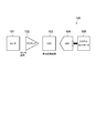
- FIG. 1 is a block diagram showing a configuration example of a sensor system applied in the present embodiment.
- the sensor system 100 includes a sensor 101, a preamplifier 102, a correlated double sampling circuit (hereinafter also referred to as CDS) 103, an AD converter (hereinafter also referred to as ADC) 104, a system controller 105, and the like.
- CDS correlated double sampling circuit
- ADC AD converter
- the preamplifier 102, the CDS 103, the ADC 104, and the system controller 105 constitute a signal processing device that processes the signal of the sensor 101.
- the preamplifier 102 may be omitted if necessary, or a circuit block other than the above may be added.
- the CDS 103 and the ADC 104 are collectively referred to as an AD conversion device.
- the sensor 101 includes various sensors that output an analog signal as a detection signal.
- a proximity sensor or a displacement sensor that outputs an AC electrical signal by utilizing magnetic induction will be described as an example.
- the preamplifier 102 amplifies the detection signal of the sensor 101, and the CDS 103 detects the difference due to the time change of the amplitude of the detection signal.
- the ADC 104 converts the signal amplitude difference detected by the CDS 103 into a digital signal and outputs the digital signal to the system controller 105.
- the system controller 105 controls the operation of the CDS 103 or the ADC 104, and is configured to recognize an object or obtain the distance to the object based on the time change of the signal amplitude obtained from the sensor 101.
- CDS is used to detect the difference of one signal due to time change.
- AFE analog front end
- CCD Charge Coupled Device
- the difference component becomes the signal component as it is, so that it is possible to reduce the influence due to individual variations of the signal source and There is an advantage that frequency noise can be suppressed.
- the CDS amplifier 1 ′ shown in FIG. 2A includes an operational amplifier (OPAMP) 2, sampling capacitors Csa and Csb, a feedback capacitor CF, and analog switches CKA, CKB, and xCKB.
- the switches CKA, CKB, xCKB are controlled at the operation timing shown in FIG.
- the sampling capacitors Csa and Csb and the switches CKA and CKB form the input stage 20 of the operational amplifier 2, and the feedback capacitor CF forms the feedback (negative feedback) circuit of the operational amplifier 2.
- the CDS amplifier 1 ′ includes a first input terminal VIP, a second input terminal VIN, a first output terminal VON connected to a negative phase output terminal of the operational amplifier 2, and a positive phase output terminal of the operational amplifier 2. And a second output terminal VOP connected to.
- VIP and VIN represent not only the notation of each input terminal described above, but also the voltage of a signal input to these input terminals.
- VON and VOP represent not only the notation of the output terminals, but also the voltages of signals output from these output terminals.
- the sensor output (voltage) is supplied to the first input terminal VIP and the second input terminal VIN.
- the switch CKA and the switch xCKB are connected in parallel to both terminals of the sampling capacitor Csa.
- the switch CKB and the switch xCKB are connected in parallel to both terminals of the sampling capacitor Csb.
- the switch CKB When the switch CKB is at the H level (ON), the input / output of the operational amplifier 2 is short-circuited (short-circuited), and the Auto-Zero mode (AZ mode, the sampling period of the CDS amplifier 1 ′, see FIG. 2B) is set and the operation is performed.
- the amplifier 2 is biased to the common potential (Vcmn). At this time, the charges accumulated in the feedback capacitance CF in the previous sequence are released.
- the voltage (Va) at the point a at that time is sampled in the sampling capacitor Csa (see FIG. 2B).
- the voltage (Vb) at the point b at that time is sampled in the sampling capacitor Csb (see FIG. 2B).
- the operational amplifier 2 At the rising edge of the switch xCKB (when the switch xCKB is at H level and ON), the operational amplifier 2 is in the amplifier mode (AMP mode, amplification period, see FIG. 2B), and the connection relationship between the sampling capacitance Csa and the sampling capacitance Csb. Is changed, the function as a CDS amplifier is established.
- Vb-Va having an amplification factor of 1
- FIG. 3 shows an example of a signal amplitude detection image using this CDS amplifier 1 '.
- the CDS amplifier 1' outputs the difference voltage between the samples, so that the change in the amplitude of the sensor output is processed by the CDS amplifier 1'as shown on the right side of FIG.
- the amount of change in amplitude ( ⁇ Vsig) This change includes the presence or absence of the target object or the distance information to the target object.
- FIG. 4 assumes signal processing that has Vmin as known information and that shifts the level by Vmin at the same time as the CDS processing. In this case, it suffices to dispose an ADC having only the resolution necessary for ⁇ Vsig, and it can be understood that the effect of reducing the resolution is extremely large as compared with the case of FIG.
- an ADC having an offset error compensation function is known for the problem in the full-scale range (see Patent Document 1 above).
- a capacitance for offset compensation is additionally provided as an additional capacitance in addition to the sampling capacitance, and offset adjustment (level shift adjustment) is performed so that the analog input amplitude falls within the ADC full scale.
- Patent Document 1 needs additional additional capacitance, which is one of the factors that increase the area. Further, the capacitance related to analog signal sampling requires a relatively large capacitance value in order to avoid an increase in thermal noise defined by kt / c. Therefore, although the approach of Patent Document 1 using this additional capacitance is suitable for solving the problem in the full-scale range, it can be said to be fatal from the viewpoint of the area of the entire circuit.
- the present embodiment is configured as follows for the purpose of providing a CDS amplifier capable of reducing the area of the entire circuit.
- FIGS. 5A and 5B are diagrams showing the configuration and the operation timing of the CDS amplifier 1A as the switched capacitor amplifier according to the first embodiment of the present technology.
- This CDS amplifier 1A is the same as the CDS amplifier 1 '(FIG. 2 (a)) of Comparative Example 1 except for the feedback circuit 3 of the operational amplifier 2.
- the CDS amplifier 1A has a feedback circuit 3 having the same configuration on the first output terminal VON side and the second output terminal VOP side.
- the CDS amplifier 1A of the present embodiment shown in FIG. 5A has a plurality of sampling capacitors Csa and Csb for sampling an analog signal (sensor signal), an operational amplifier 2, and a feedback circuit 3.
- the feedback circuit 3 has a capacitance array 31 and a switch group 4.
- the capacitance array 31 has capacitance elements (feedback capacitances CF / 2, CF / 4, ..., CF / 2 n , CF / 2 n ) weighted by 2 n (n is an integer).
- Each capacitance element is connected in parallel between the input side and the output side of the operational amplifier 2.
- One end of each capacitive element is connected to the input side of the operational amplifier 2, and the other end is individually connected to a plurality of switches that form the switch group 4.
- the combined capacitance of the capacitance array 31 is the same as the feedback capacitance CF of the CDS amplifier 1 ′ according to the comparative example 1 shown in FIG.
- the capacitance array 31 is configured to be able to charge a level shift amount of electric charges corresponding to the minimum voltage amplitude Vmin (see FIG. 3) of the detection signal of the sensor 101.
- the level shift amount is digital data (L / S Data, known information) having a resolution of n bits. A specific method for estimating the level shift amount will be described later in the fourth embodiment according to the present technology.
- the switch group 4 is composed of analog switches serially connected to the other end of each capacitive element that constitutes the capacitive array 31.
- the plurality of switches forming the switch group 4 have three connection destinations.
- the three connection destinations are the first reference potential VT, the second reference potential VB lower than the first reference potential VT, and the output terminal of the operational amplifier 2.
- the operational amplifier 2 is subjected to negative feedback by the feedback capacitor (capacitance array 31) and one connection destination of the switch group 4 (the output end of the operational amplifier 2) to detect the difference in amplitude of the sensor signal (analog signal). Is composed of.
- the operational amplifier 2 has two states, a period for sampling an analog signal (AZ mode) and a period for amplifying a sampled analog signal (AMP mode).
- the sampling capacitors Csa and Csb each hold two analog signals having different time axes.
- the operational amplifier 2 calculates the difference between the holding voltage obtained by the first sampling (one sampling capacitance Csa) and the holding voltage obtained by the second sampling (the other sampling capacitance Csb) as the feedback capacitance (capacity array 31). Amplify with the capacity ratio of.
- connection destinations of the plurality of switches are individually controlled by a controller (not shown) (corresponding to the system controller 105 shown in FIG. 1).
- the controller uses a data signal (L) for precharging the feedback capacitor (capacitance array 31) with a level shift amount of charge corresponding to a predetermined amplitude value (minimum voltage amplitude Vmin in this example) of the sensor signal (analog signal). / S Data) is configured to be able to be generated.
- the first reference potential VT is the maximum voltage (high potential end) for defining the level shift amount (range)
- the second reference potential VB is the minimum voltage for defining the level shift amount. (Low potential end).
- the number of connection destinations of each switch is not limited to three, and may be four or more, as long as the potential of each connection destination is different.
- the operation timing of the CDS amplifier 1A is controlled by the operation timing shown in FIG. 5B, similarly to the operation sequence of the CDS amplifier 1 ′ according to the comparative example 1 described above.
- the switch CKB when the switch CKB is at the H level, the input and output of the operational amplifier 2 are short-circuited, and the Auto-Zero mode (AZ mode) is set, and the operational amplifier 2 is biased to the common potential (Vcmn).
- the other end of the switches forming the switch group 4 is connected to the first reference potential VT or the second reference potential VB according to L / S Data, and the level is added to the capacitance array 31 weighted by 2 n.
- the shift amount is precharged as an electric charge.
- the level shift amount is matched with the capacitance array 4 by the switch.
- the charge is accumulated. Since the level shift amount is digital data having a resolution of n bits, desired charges can be accumulated by the capacitive element weighted by 2 n .
- the voltage (Va) at the point a is sampled in the sampling capacitor Csa at the falling edge of the switch CKA.
- the voltage (Vb) at the point b is sampled in the sampling capacitor Csb at the falling edge of the switch CKB.
- V LS is a level shift voltage determined by n-bit L / S Data (D n-1 , D n-2 , ..., D 0 ) (see the following equation).
- the level shift amount is subtracted when the sampled signal is transferred. This eliminates the need to assume a full scale that covers the entire CDS output including the level shift amount corresponding to the minimum voltage amplitude Vmin (see FIG. 3) output from the sensor 101. It is possible to reduce power consumption by eliminating the need for an ADC having
- the feedback capacitance in realizing the level shift function described above, and the feedback capacitance is arrayed (divided) to precharge the level shift amount as digital data. That is, the level shift function can be realized without requiring the additional capacitance described in Patent Document 1.
- the capacitance array 31 serves as the feedback capacitance of the operational amplifier 2, it is structurally equivalent to the conventional CDS amplifier, and the capacitance value as CF does not change.
- both the CDS function and the level shift function can be realized without any additional capacity. This makes it possible to detect only the signal amplitude change ( ⁇ Vsig) from the sensor 101. Further, since the full scale of the ADC arranged in the subsequent stage can be tuned only for the amplitude change, the specifications required for the ADC can be significantly relaxed. These measures will greatly contribute to the reduction of power consumption and the reduction in area of the entire circuit as an amplitude detection system.
- FIG. 6 is a diagram showing a configuration of a switched capacitor amplifier 1B having a level shift function, which is a second embodiment according to the present technology.
- This switched capacitor amplifier 1B is the same as the CDS amplifier 1A according to the first embodiment, except for the peripheral configuration (sampling unit capacitance network 5) of the sampling capacitance Cs as the input stage of the operational amplifier 2.
- the sampling unit capacitance network 5 is provided with one sampling capacitance Cs for each of the first and second input terminals VIP, VIN, one end of the sampling capacitance Cs being connected in parallel to the two analog switches CKA, xCKB, and the other. The end is connected to the input side of the operational amplifier 2.
- One of the two analog switches (CKA) is connected to VIN, and the other one (xCKB) is connected to the common potential.
- the switched capacitor amplifier 1B composed of the sampling capacitor Cs and the feedback circuit 3 shifts the voltage sampled by the sampling capacitor Cs to an arbitrary level, similarly to the operation of the CDS amplifier 1A of the first embodiment. Is possible. Obviously, the configurations of the sampling capacitor Cs and the two switches CKA and xCKB in the sampling unit network 5 are not limited to this.
- FIG. 7 is a diagram showing a configuration of a CDS amplifier 1C having a level shift function as a switched capacitor amplifier according to the third embodiment.
- the CDS amplifier 1C is the same as the switched capacitor amplifier 1B of the second embodiment except the connection destination of the input / output of the operational amplifier 2.
- the operational amplifier 2 is short-circuited at the timing of the AZ mode, but the CDS amplifier 1C according to the present embodiment has the operational amplifier 2 at the timing of the AZ mode.
- the input and output sides of are connected to the common potential via switches SW1 and SW2, respectively.
- the operational amplifier 2 is not necessary (not connected to other circuits) at the timing of the AZ mode, so that it is not necessary to consider the stability of the negative feedback loop of the circuit, and the degree of difficulty in circuit design is eased. .
- FIG. 8 shows an exemplary level shift amount estimation system 6 for effectively incorporating the level shift function of the CDS amplifier 1A described in the first embodiment. Since the system 6 has the same configuration and operation on the CDSOUTN side and the CDSOUTP side, which are the output terminals of the CDS amplifier 1A, the description will be simplified and only one of the CDSOUTN side will be described.
- the system 6 includes an n-bit ADC 7 that digitizes the output voltage of the CDS amplifier 1A, a reference voltage (VREF_LS) generation source 61 that generates a level shift range, a reference voltage (VREF_ADC) generation 62 that generates a full scale of the ADC 7, And a system sequence controller 8.
- the system sequence controller 8 is typically composed of a computer having a CPU, a memory, and the like.
- the system sequence controller 8 may have a configuration corresponding to the system controller 105 shown in FIG.
- the system 6 has two operation states, that is, an operation for estimating a shift amount (1st Sequence) and an amplitude detection normal operation (2nd Sequence), and is managed by the system sequence control unit 8 to set a full scale of a reference voltage. Set it appropriately.
- the control flow will be described in detail below.
- Step S1 “1st Sequence” (estimation of shift amount)
- Step S2 The sensor output is set under the condition that the sensor signals input to the input terminals CDSIP and CDSIN have the minimum voltage amplitude.
- Step S2 VREF_LS is set.
- Step S3 The data setting for n-bit L / S is set to code-free (any code may be used, for example, all zeros).
- Step S4 VREF_ADC (VT_AD, VB_AD) is set.
- the maximum amplitude of the CDS amplifier 1D assumed in the system is set.
- Step S5 The amplitude detection operation is started. At this time, the converted data of the ADC 7 is left in the internal register or the like as Dmin.
- Step S6 The sensor output is set under the condition that the sensor signal has the maximum voltage amplitude.
- Step S7 The amplitude detection operation is started. At this time, the converted data of the ADC 7 is left in the internal register or the like as Dmax.
- the steps S2 and S3 may be set as the following steps S2 ′ and S3 ′. That is, in the combination of the setting of VREF_LS and the n-bit L / S data, the shift amount of zero may be satisfied as a condition.
- Step S2 ′ VREF_LS is set.
- Step S3 ' n-bit L / S data is set.
- a code corresponding to 2 n / 2 (for example, code 128 in the case of 8 bits) is set.
- the AD conversion operation in steps S5 and S7 is performed a plurality of times, and the data processing method is made one such as making the data of the several times the true value or making the average value of several data the true value. Not limited.
- Approximate level shift amount is estimated (calibrated) in this 1st Sequence, and the original operation of amplitude detection is executed using that information.
- Step S11 “2nd Sequence” (actual operation of amplitude detection)
- Step S12 VREF_ADC used in the 1st Sequence is set.
- Step S12 VREF_ADC is set to a value obtained by the Dmax-Dmin calculation + a margin amount ( ⁇ ) ( ⁇ Vsig + ⁇ ).
- Step S13 The shift amount is set to Dmin + ⁇ .
- Step S14 The amplitude detection operation is started.
- the resolution of the ADC 7 may be the resolution of the accuracy required by the 2nd Sequence, and it is not necessary to have an accuracy higher than the resolution required by the 2nd Sequence in the 1st Sequence.
- both the CDS function and the level shift function can be realized without any additional capacity. This makes it possible to detect only the signal amplitude change from the sensor. Further, since the full scale of the ADC 7 arranged in the subsequent stage can be detected only for the amplitude change, the performance required for the ADC 7 is significantly eased. As a result, compared with Comparative Example 1, for example, the amplitude detection system greatly contributes to lower power consumption and smaller area.
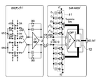
- Comparative example 2 shows configuration examples of the CDS amplifier 1'and the ADC 9'as Comparative Example 2 and their operation timings.
- the configuration and operation of the CDS amplifier 1' is the same as that of Comparative Example 1 (FIGS. 2A and 2B), and thus the description thereof is omitted.
- the ADC 9' has several options as a conversion method, but here, the AD converter (SAR-ADC) of the successive approximation method (SAR) having the binary weight capacitance array type DA converter (C-DAC) is taken as an example. To do.
- the conversion method of Comparative Example 2 and the sequence of the sequential operation thereof are not limited to this.
- the SAR-ADC 9' is an n-bit binary weight capacitance DA converter C-DAC10 (2 n-1 Cu, 2 n-2 Cu, ..., 2Cu, based on a unit capacitance Cu which also has a sampling function).
- Cu, Cu a comparator (CMP) 11 that determines the magnitude relationship of difference signals
- CMP comparator
- CTRL controller
- the C-DAC 10 is connected to the first and second output terminals VON and VOP of the CDS amplifier 1 ′ via a switch xCKAD, and based on a control signal (Successive Data) from the controller 12, each capacitance has two reference values.
- the switch group 41 includes a plurality of switches that can be selectively switched to the potential (VT, VB).
- the switch xCKAD is at the H level, and all the capacitors configuring the C-DAC 10 are connected to the reference potential VT, whereby the initial state is set.
- the controller 12 samples the output voltage (VOP, VON) of the CDS amplifier 1 ′ with respect to the reference voltage VT, and starts the binary search sequence.
- the MSB is determined by directly determining the magnitude relationship of the voltage after sampling without any involvement of the C-DAC 10 in the first comparison determination for determining the MSB (most significant bit).
- the connection destination of 2 n-1 Cu connected to the higher potential terminal of the two input terminals of the comparator 11 is switched from the reference potential VT to the reference potential VB.
- the capacitors connected to the terminals with lower potentials at the two input terminals of the comparator 11 retain the state of being connected to the reference potential VT.
- This switch action causes charge sharing and subtracts the voltage corresponding to the most significant bit of C-DAC 10 from the first sampled voltage.
- the VOP side and the VON side are not complementary sequences, and only the capacitance on one side of the input end of the comparator 11 is switched from the reference potential VT to the reference potential VB.
- the comparator 11 determines the magnitude relationship of the voltage after the subtraction, and the next bit (2nd-MSB) (one bit lower than the most significant bit) is determined.
- the connection destination of 2 n ⁇ 2 Cu connected to the terminals of the two input terminals of the comparator 11 with the higher potential is switched from the reference potential VT to the reference potential VB, and the lower potential
- the capacitance connected to the terminal is maintained in the state of being connected to the reference potential VT.
- charge redistribution is performed, and the voltage corresponding to 2nd-MSB of the C-DAC 10 is further subtracted from the previously subtracted voltage.
- connection destination of the binary weight capacitor is held (stay) at the reference potential VT, switching from the reference potential VT to the reference potential VB, and the C-DAC 10 according to the comparison determination result of the comparator 11.
- the digital data is determined (ADC_OUT) by repeating the subtraction by the charge sharing action of (2) (binary search).
- the SAR-ADC 9 ′ it has a large demerit and it is necessary to perform resampling in the SAR-ADC 9 ′, so that the arrangement of the feedback capacitance CF and the binary weight capacitance of the C-DAC 10 becomes redundant. Since these capacitances are related to kT / C noise, there is no choice but to choose a relatively large capacitance value, and in order to prevent signal quality deterioration due to resampling, the total capacitance value of C-DAC 10 should be a value below CF. Cannot be done (CF ⁇ 2 n Cu). As a result, the area of the entire circuit is increased, which is not desirable.
- the present embodiment is configured as follows for the purpose of providing an AD converter capable of reducing the area of the entire circuit.
- FIGS. 10A and 10B are diagrams showing the configuration and the operation timing of the AD conversion device 14A according to the fifth embodiment of the present technology.
- the AD conversion apparatus of this embodiment corresponds to the CDS 103 and the ADC 104 in the sensor system 100 shown in FIG.
- a configuration example in which a CDS amplifier having a flip (Flip) capacitance and a successive approximation type ADC (SAR-ADC) are integrated will be described.
- the AD converter 14A of this embodiment includes a plurality of sampling capacitors Csa and Csb for sampling an analog signal (sensor signal), an operational amplifier 2, a feedback circuit 3F, a comparator 11, and a controller 12.
- the feedback circuit 3F has a capacitance array 31 and a switch group 4.
- the input stage 20 of the CDS amplifier has the same configuration as that of Comparative Example 2.
- the AD converter 14A has a feedback circuit 3F having the same configuration on the first output terminal VON side and the second output terminal VOP side of the operational amplifier 2, respectively.
- the feedback circuit 3F has a capacitance array 31 and a switch group 4. Since the AD converter 14A has the same configuration and operation on the VON side and the VOP side, the description will be simplified and only the different configuration on the VON side will be described.
- the capacitance array 31 has the same configuration as that of the first embodiment and has a plurality of 2 n weighted capacitance elements (feedback capacitance CF or Flip capacitance, CF / 2, CF / 4, ..., CF / 2). n , CF / 2 n ).
- Each capacitance element is connected in parallel between the input side and the output side of the operational amplifier 2.
- One end of each capacitive element is connected to the output side of the operational amplifier 2, and the other end is individually connected to a plurality of switches that form the switch group 4.
- the switch group 4 is composed of a plurality of analog switches serially connected to the other end of each capacitive element that constitutes the capacitive array 31.
- the plurality of switches forming the switch group 4 have three connection destinations as in the first embodiment.
- the three connection destinations are the first reference potential VT, the second reference potential VB, and the input terminal of the operational amplifier 2.
- the first reference potential VT and the second reference potential VB are the high potential end and the low potential end of the reference voltage that defines the full scale of AD conversion, respectively.
- Connection destinations of the plurality of switches are individually controlled by the controller 12.
- the operational amplifier 2 is subjected to negative feedback by the feedback capacitor (capacitance array 31) and one connection destination of the switch group 4 (the output end of the operational amplifier 2) to detect the difference in amplitude of the sensor signal (analog signal). Is composed of. As will be described later, the comparator 11 is configured to determine the magnitude relationship of the difference between the output signals of the operational amplifier 2.
- the controller 12 samples the analog signal by the plurality of sampling capacitors Cs, the period in which the sampled analog signal is amplified by the operational amplifier 2 according to the ratio of the plurality of sampling capacitors Cs and the feedback capacitor CF, and the amplified analog signal.
- the period for AD conversion is controlled based on the output of the comparator 11.
- the operational amplifier 2 amplifies the difference between the holding voltage obtained in the first sampling and the holding voltage obtained in the second sampling by the capacitance ratio with the feedback capacitance CF.
- the controller 12 controls the feedback capacity in a binary search sequence according to the determination result of the comparator 11.
- the switch CKC (first switch) is connected between the input and output ends of the operational amplifier 2 so as to be in parallel with the feedback circuit 3F.
- a switch xCKAD is arranged between the output terminal of the operational amplifier 2 and the comparator 11.
- the AD conversion apparatus 14A of the present embodiment has a function equivalent to the SAR-ADC 9'of Comparative Example 2 re-sampling the operation information of the CDS amplifier (Flip operation).
- the feedback capacitance CF into a capacitance array as the resolution required for the SAR-ADC, no inconvenience occurs in the binary search sequence of the SAR-ADC. Further, only the analog switch is used as the additional part, and the total capacitance value as the feedback capacitance CF does not change and is simply arrayed. Therefore, an unnecessary overhead (cost) is not required, and the area reduction effect by sharing the feedback capacitance CF and the C-DAC is extremely large.
- the voltage (Va) at the point a is sampled at Csa at the falling edge of the switch CKA, and the voltage (Vb) at the point b is sampled at Csb at the falling edge of the switch CKB.
- the switch xCKAD is at the H level
- the feedback capacitance CF is connected to the input / output terminal of the operational amplifier 2 and the feedback control of the operational amplifier 2 is effective.
- the switch CKC is at the H level
- the input / output terminal of the operational amplifier 2 is short-circuited and the Auto-Zero mode (AZ mode) is set, and the operational amplifier 2 is biased to the common potential (Vcmn, common potential).
- the charges accumulated in the feedback capacitance CF in the sequence are released.
- the operational amplifier 2 enters the AMP mode at the rising edge of the switch xCKB, and the sampling capacitor Csa and the sampling capacitor Csb are connected to the input terminals of the operational amplifier 2, respectively, so that the arithmetic processing is performed by the charge transfer to the feedback capacitor CF.
- a voltage of Vb-Va is obtained at the differential output (VOP-VON) of the CDS amplifier.
- the conversion mode flip & Conv., AD conversion period, see FIG. 10B
- the binary search is performed.
- the switches CKC and xCKB connected to the input / output terminals of the operational amplifier 2 are turned off, and the feedback control by the operational amplifier 2 is in the invalid period. From this timing, the capacitance array 31 functioning as the feedback capacitance CF of the CDS amplifier becomes a weighted capacitance array having the calculation information of the CDS amplifier, and is directly controlled by the controller 12 according to the determination result of the comparator 11.
- the reference voltage terminal of the capacitor CF / 2 of the MSB is connected to the reference potential VT, and the reference voltage terminals of the other capacitors CF are connected to the reference potential VB.
- Charge distribution is performed by this switch action, and a voltage corresponding to the MSB of the C-DAC, that is, 1/2 full scale is subtracted from the operation information voltage of the CDS amplifier.
- the comparator 11 determines the magnitude relationship of the voltage after the subtraction, and the MSB is determined.
- the reference potential of the MSB capacitor CF / 2 is directly connected to the stay or VB according to the determination result of the MSB, and the reference potential of the 2nd-MSB capacitor CF / 4 is connected to VT. Charge distribution is performed by this switch action, and a voltage corresponding to 2nd-MSB of the C-DAC, that is, 1/4 full scale is subtracted.
- the comparator 11 determines the magnitude relationship of the voltages after the subtraction, and 2nd-MSB is determined. The same sequence is performed thereafter, and the reference potential of the feedback capacitance CF is stayed at VT or switched to VB according to the comparison determination result of the comparator 11, and the input terminal difference of the comparator 11 by the charge distribution action of the C-DAC is performed. Digital data is determined by repeating the voltage subtraction operation.
- the binary search sequence is not limited to the one described above, and any mechanism that directly controls the feedback capacitance CF of the CDS amplifier as a capacitance array may be used.
- the switching of xCKAD is a completely exclusive operation. That is, the operational amplifier 2 and the comparator 11 only need to be in the active state for a necessary period, and during the operation period of the CDS amplifier, the bias current of the comparator 11 is cut off to put the comparator 11 in the standby state.
- the bias current of the operational amplifier 2 is cut off, and the operational amplifier 2 is put in the standby state.
- both the operational amplifier 2 and the comparator 11 may be replaced by a single circuit, and in this case, it is also effective from the viewpoint of reducing the circuit scale. Target.
- C-DAC capacitance array
- FIG. 11 is a diagram showing a configuration of a CDS amplifier having a flip capacitor and an SAR-ADC integrated AD conversion device 14B according to a sixth embodiment of the present technology.
- configurations different from those of the fifth embodiment will be mainly described, and configurations similar to those of the fifth embodiment will be denoted by the same reference numerals and description thereof will be omitted or simplified.
- the switched capacitor amplifier (SCA) using the operational amplifier 2 often has a problem that the offset voltage (Vos) of the operational amplifier narrows the output dynamic range. In this case, the offset voltage automatic compensation technique is relatively frequently used. Also in the present technology, it is possible to provide this function without changing the operation timing. Therefore, in the AD converter 14B of the present embodiment, one end of the two selectable auxiliary (analog) switch group 42 is connected to the output end side of the operational amplifier 2 of the feedback capacitance CF.
- the auxiliary switch group 42 is arranged between the capacitance array 31 and the output terminal of the operational amplifier 2.
- the auxiliary switch group 42 is composed of a plurality of switches that are respectively connected to the plurality of capacitive elements that form the capacitive array 31. These plural switches have two connection destinations, one (CKC) is connected to the common potential Vcmn, and the other (xCKB) is connected to the output terminal of the operational amplifier 2.
- the auxiliary switch group 42 is connected to the common potential by the controller 12 during the analog signal sampling period (AZ mode).
- the feedback capacitor CF is precharged with a voltage of “Vcmn ⁇ Vos”.
- the connection processing of the auxiliary switch group 42 is switched to the output terminal of the operational amplifier 2 to perform the arithmetic processing as the above-mentioned CDS amplifier.
- the offset voltage (Vos) does not change in the AZ mode period and the AMP period, the voltage precharged in the feedback capacitor CF during charge transfer in the AMP period is subtracted, and the output dynamic range of the operational amplifier 2 is reduced. Does not need to be narrow.
- the automatic compensation function of the offset voltage of the operational amplifier 2 can be added while the circuit scale is reduced similarly to the fifth embodiment. it can.
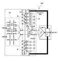
- FIG. 12 is a diagram showing a configuration of an integrated AD conversion device 14C of a CDS amplifier having a flip capacitor and a SAR-ADC, which is a seventh embodiment according to the present technology.
- configurations different from those of the fifth embodiment will be mainly described, and configurations similar to those of the fifth embodiment will be denoted by the same reference numerals and description thereof will be omitted or simplified.
- one end (output side) of the feedback capacitance CF (capacitance array 31) weighted by 2 n is output via the output end of the operational amplifier 2 and the switch CKC (second switch). It is connected to the common potential (Vcmn).
- One of the other ends (input side) of the switch group 4 having three connection destinations is connected to the common potential (Vcmn) via the input end of the operational amplifier 2 and the switch CKB (third switch).
- the second switch and the third switch are controlled by the controller 12.
- the input / output terminal of the operational amplifier 2 is short-circuited at the timing of the AZ mode, but as shown in FIG. 12, the input / output terminal of the operational amplifier 2 at the timing of the AZ mode. However, they may be connected to the common potential (Vcmn) via the switches CKB and CKC.
- the operational amplifier 2 is not necessary at the timing of the AZ mode, so that it is not necessary to consider the stability of the negative feedback loop, and the degree of design difficulty is eased. Furthermore, since the operational amplification function itself can be stopped even in the AZ mode period, it is possible to develop a switched operational amplifier configuration in which the bias current is cut off on the time axis, which is effective for low power applications.
- AD conversion device 14C of the present embodiment configured as described above, it is possible to reduce the degree of design difficulty and reduce power consumption while reducing the circuit scale as in the fifth embodiment.
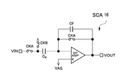
- FIG. 13A shows a configuration of a switched capacitor amplifier (SCA) 16 as a comparative example 3
- FIG. 13B shows a configuration of a comparator-based switched capacitor amplifier (CB-SCA) 17 as a comparative example 4.
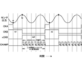
- FIG. 13C shows their operation timing.
- the CDS is often based on a switched capacitor amplifier including an operational amplifier (OPAMP) 2, a feedback capacitance CF, a sampling capacitance Cs, and switches (CKA, CKB).
- OPAMP operational amplifier
- CF feedback capacitance
- Cs sampling capacitance
- CKA sampling capacitance
- the switch CKA When the switch CKA is at the H level, the input / output terminal of the operational amplifier 2 is short-circuited, and the Auto-Zero mode (AZ) is set, and the sampling capacitor Cs is charged with VIN-VAG at the falling edge of the switch CKA.
- the amplifier mode (AMP) When the switch CKB is at the H level, the amplifier mode (AMP) is set, and the voltage defined by the following equation is output by the charge transfer action.
- the CB-SCA 17 shown in FIG. 13 (b) aims at the non-OPAMP conversion and solves the problems (1) and (2) of the operational amplifier described above. It can be combined with a ladder type DA converter (DAC) 15.
- DAC ladder type DA converter
- the comparator (CMP) 11 determines the magnitude relationship of two inputs and outputs an H or L logic level. Therefore, it is not necessary to secure the output linear range unlike the operational amplifier. Further, since the comparator 11 is close to the logic operation, it is very convenient because it can benefit from the Technology Node such as lower power supply voltage. Furthermore, the difficulty of designing parameters such as high gain, wide band, and loop stability is reduced.
- FIG. 13B shows the method, and the CB-SCA 17 includes a sampling capacitor Cs, a feedback capacitor CF, clocks CKA and CKB, a comparator (CMP) 11, and a controller (CTRL) 12 that controls a binary search sequence. , And a DA converter 15, and is basically controlled by switches CKA and CKB as in the SCA 16 described above.
- the switch CKA is at the H level and the feedback capacitance CF is short-circuited
- the summing node end (SN) is connected to VAG to enter the AZ mode, and the charge of the feedback capacitance CF in the previous sequence is released.
- the sampling capacitor Cs is charged with the voltage “VIN ⁇ VAG” at the falling edge of the switch CKA.
- the connection of the feedback capacitor CF is switched to the DA converter 15, and the binary search sequence by the comparator 11 and the DA converter 15 is started.
- the following voltage is applied to the end of the summing node via Cs, and the comparator 11 compares and determines the magnitude relationship using VAG as a reference voltage, and outputs data sequentially from the MSB of DAC resolution.
- Vsum is the voltage at the end of the summing node.
- the subtraction operation is repeated for n bits until Vsum becomes zero according to the determination result of the comparator 11.
- the DAC output is given by the following equation, and the same result as the equation (3) can be obtained.
- the CB-SCA 17 performs time-divisional charge transfer according to the determination result of the comparator 11, unlike charge transfer by a continuous feedback action of the operational amplifier.
- the control system is complicated as described above, the CB-SCA signal processing can obtain the same result as the OPAMP-based SCA.
- the non-OPAMP configuration is used, the breakthrough effect on the above-described operational amplifier problem is great.
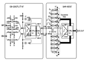
- FIGS. 14A and 14B show configurations of CB-CDS amplifier 19 'and SAR-ADC 9'using CB-SCA and their operation timings as Comparative Example 5.
- the CB-CDS amplifier 19 includes a sampling capacitor (Csa, Csb), a feedback capacitor CF, a comparator (CMP) 11, a controller (CTRL) 12 for controlling a binary search sequence, an analog switch (CKA, CKB), and a DA converter. (DAC) 15 is provided.
- the CB-CDS amplifier 19 ' is basically controlled by the switches CKA and CKB, like the CB-SCA 17 described above.
- the switch CKB is at the H level, the feedback capacitance CF is short-circuited, and the summing node end is connected to the common potential (Vcmn) to enter the AZ mode (see FIG. 14B), and is accumulated in the feedback capacitance CF in the previous sequence. The charge is released.
- the voltage (Va) at the point a is sampled in the sampling capacitor Csa at the falling edge of the switch CKA, and the voltage (Vb) at the point b is sampled in the sampling capacitor Csb at the falling edge of the switch CKB.
- the switch xCKB is at the H level in the AMP period, the connection of the feedback capacitance CF is switched to the DA converter 15, and the binary search sequence by the comparator 11 and the DA converter 15 controlled by CKAMP is started.
- the voltage of Expression 6 below is transmitted to the summing node end via the sampling capacitors Csa and Csb, and the comparator 11 compares and determines the magnitude relationship of the voltage difference (Vsumd) generated at the summing node, and the MSB of the DAC resolution.
- the data is output in order from.
- CKAMP is a signal clock that controls the comparator for the binary search sequence, and corresponds to the binary search control signal in FIG. CKAMP controls the comparator 11 during the AMP period of the CDS amplifier, and sequentially determines the magnitude relationship between the summing nodes (see FIG. 14B).
- the differential output (VOP-VON) of the DA converter 15 is given by the following equation.
- the voltage Vb-Va is obtained at VOP-VON. In this way, the function as the CDS is realized with the non-OPAMP configuration.
- the SAR-ADC 9 ′ on the right side of FIG. 14 (a) has the same configuration and AD conversion method as in Comparative Example 2, and a description thereof will be omitted.
- the comparator 11 in the SAR-ADC 9' is controlled by CKSAR.
- CKSAR is a signal clock that controls the comparator for the binary search sequence, controls the comparator 11 during the AD conversion period, and sequentially determines the magnitude relationship of the input terminals of the comparator 11 (FIG. 14B). reference).
- both the CB-CDS amplifier 19 ′ and the SAR-ADC 9 ′ have a redundant configuration having the function of the binary search sequence based on the comparator and the DA converter 15.
- the feedback capacitance CF that holds the analog voltage, and the capacitance array of the C-DAC 10 of the SAR-ADC 9' are associated with kT / C noise, so there is no choice but to choose a relatively large capacitance value.
- This large capacitance value undesirably increases the area of the entire circuit as in Comparative Example 2, as a result.
- the present embodiment is configured as follows for the purpose of providing an AD converter capable of reducing the area of the entire circuit.
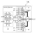
- FIG. 15A and 15B are diagrams showing the configuration and the operation timing of the AD conversion device 18 according to the eighth embodiment of the present technology.
- the AD converter 18 of the present embodiment corresponds to the CDS 103 and the ADC 104 in the sensor system 100 shown in FIG.
- a configuration example in which the CB-CDS amplifier and the SAR-ADC are integrated will be described.
- the AD converter 18 of this embodiment includes an input stage 20 including a plurality of sampling capacitors Csa and Csb for sampling an analog signal (sensor signal), a feedback circuit 3F, a comparator (CMP) 21, and a controller (CTRL). 22 and.
- the feedback circuit 3F has a capacitance array 31 and a switch group 4.
- Capacitor array 31 has the same configuration as the first embodiment, capacitive elements that are weighted by 2 n (feedback capacitance CF, CF / 2, CF / 4, ⁇ , CF / 2 n, CF / 2 n ). Each capacitance element is connected in parallel to the input side of the comparator 21. One end of each capacitive element is connected to the input side of the comparator 21, and the other end is individually connected to a plurality of switches that form the switch group 4.
- the switch group 4 is composed of a plurality of analog switches serially connected to the other end of each capacitive element that constitutes the capacitive array 31.
- the plurality of switches forming the switch group 4 have three connection destinations as in the first embodiment.
- the three connection destinations are the first reference potential VT, the second reference potential VB, and the input terminal of the comparator 22.
- the first reference potential VT and the second reference potential VB are the high potential end and the low potential end of the reference voltage that defines the full scale of AD conversion, respectively.
- the connection destinations of the plurality of switches are individually controlled by the controller 22.
- the comparator 21 is configured to determine the magnitude relationship between the analog signals sampled by the sampling capacitors Csa and Csb, as described later.
- the controller 22 controls a period for sampling an analog signal by the sampling capacitors Csa and Csb and a period for AD-converting the sampled analog signal based on the output of the comparator 21.
- the controller 22 is configured to connect the switch group 4 to the input terminal of the comparator 21 during the sampling of the analog signal.
- the AD conversion device 18 is a circuit in which the CB-CDS amplifier and the SAR-ADC are shared. There are two parts of interest for commonization, and one is a comparator 21 and a controller 22 for performing a binary search process. The other one is a C-DAC shared by re-sampling the DAC and the feedback capacitance CF that generate the operation voltage of the CDS amplifier.
- the feedback capacitance CF is composed of the capacitance array 31 divided into capacitances weighted by 2 n and the switch group 4 including a plurality of switches having three connection destinations.
- One end (input side) of the weighted capacitance CF is connected to the input end of the comparator 21, and the other end (output side) is connected to one end of the switch group 4 having three connection destinations.
- One of the other ends of the switch group 4 having three connection destinations is connected to the input end of the comparator 21 in order to release the charge in the AZ mode.
- the other two are connected to the maximum reference potential (VT) or the minimum reference potential (VB) that defines the DAC full scale (FS) according to the determination result of the binary search.
- the comparator 21 is connected to the common potential Vcmn not only on the input terminals VIP and VIN sides but also via the switch CKB.
- the switch CKB is at the H level
- the input terminal of the comparator 21 is connected to the common potential Vcmn via the switch CKB
- the AZ mode is set.
- the switch group 4 having three connection destinations, only the switch connected to the input terminal of the comparator 21 is turned on, and the charge accumulated in the previous sequence is released.
- the voltage (Va) at the point a is sampled in the sampling capacitor Csa at the falling edge of the switch CKA, and the voltage (Vb) at the point b is sampled in the sampling capacitor Csb at the falling edge of the switch CKB.
- the AD conversion device 18 enters the AMP mode, the connection relationship between the sampling capacitors Csa and Csb changes, and the difference in the sampled voltage is transmitted to the input terminal of the comparator 21 controlled by CKAMP (Vsumd).
- the connection destination of the switch group 4 having three connection destinations is changed, and the binary search sequence is started. Since the control of the capacitance array 31 has a complementary relationship between the positive phase side and the negative phase side, the sequence will be described below only for the positive phase side.
- the feedback capacitance (CF / 2) corresponding to MSB is connected to the first reference potential VT, and the other feedback capacitances are connected to the second reference potential VB.
- Charge distribution is performed by this switch action, and the voltage corresponding to MSB, that is, 1/2 full scale, is subtracted from Vsumd by the capacitance ratio via the feedback capacitance CF as described above.
- the comparator 21 determines the magnitude relationship of the voltage after the subtraction, and the MSB is determined.
- the reference voltage of the feedback capacitor corresponding to the MSB is directly connected to the stay or the second reference potential VB according to the determination result of the MSB, and the reference voltage of the feedback capacitor corresponding to 2nd-MSB is set. It is connected to the first reference potential VT. Charge distribution is performed by this switch action, and a voltage corresponding to 2nd-MSB, that is, 1/4 full scale is subtracted by the capacitance ratio via CF.
- the comparator 21 determines the magnitude relationship of the voltages after the subtraction, and 2nd-MSB is determined. The same sequence is performed thereafter, and the reference voltages of the plurality of feedback capacitors are stayed at VT or switched to VB according to the comparison determination result of the comparator 21, and the CMP input terminal difference voltage is subtracted by the charge distribution action of the capacitor array. Digital data is determined by repeating the operation.
- the binary search sequence is not limited to the one described above, and may be any mechanism that directly controls the feedback capacitance CF as a capacitance array.
- the present technology enables the circuit to have both the CDS operation function and the AD conversion function even though the circuit is one SCA. Further, by forming the feedback capacitance CF into a capacitance array as a resolution required for SAR, no inconvenience occurs in the binary search sequence of SAR.
- the CDS calculation process of two sample voltages Vb-Va has been described, but the CDS calculation function is not limited to this.
- the addition / subtraction process may be performed by using N (N is an integer of 2 or more) sample capacitors and switches, and using the sampled voltages.
- the AD conversion device 18 of the present embodiment it is possible to achieve both the CDS calculation function and the AD conversion function, even with one SCA. At that time, by forming the feedback capacitance CF into a capacitance array as a resolution required for SAR, no inconvenience occurs in the binary search sequence of SAR.
- the only additional parts are analog switches, and the total capacitance value as the feedback capacitance CF is simply arrayed. Therefore, the effect of reducing the power and area by sharing the capacitor is large, such as unnecessary extra overhead.
- the present technology may have the following configurations.
- a plurality of sampling capacitors for sampling an analog signal A feedback capacitance that is a capacitance array, A switch group connected to the feedback capacitor and having at least three connection destinations;
- a switched capacitor amplifier comprising: an operational amplifier that performs negative feedback by one connection destination of the feedback capacitor and the switch group and detects a difference in amplitude of the analog signal.
- the switched capacitor amplifier according to (1) above The feedback capacitor is a switched capacitor amplifier having a plurality of capacitive elements weighted to a power of 2 (n is an integer).
- the switched capacitor amplifier according to (3) above The other connected destination of the switch group is a switched capacitor amplifier which is an output terminal of the operational amplifier.
- the switched capacitor amplifier according to (5) above, The operational amplifier is a switched capacitor amplifier having two states, a period for sampling the analog signal and a period for amplifying the sampled analog signal.
- Each of the plurality of sampling capacitors has a capacity for holding two analog signals having different time axes
- the operational amplifier is a switched capacitor amplifier that amplifies a difference between a holding voltage obtained in the first sampling and a holding voltage obtained in the second sampling by a capacitance ratio with the feedback capacitance.
- a plurality of sampling capacitors for sampling an analog signal A feedback capacitance that is a capacitance array, A switch group connected to one end of the feedback capacitor and having at least three connection destinations; An operational amplifier which performs negative feedback by one connection destination of the feedback capacitor and the switch group and detects a difference in amplitude of the analog signal; An A / D converter including a comparator for determining a magnitude relation of a difference between output signals of the operational amplifier.
- the feedback capacitor includes a plurality of capacitive elements weighted to the n-th power of 2 (n is an integer).
- the AD converter according to (12) above An AD converter in which the controller controls the feedback capacitance in a binary search sequence according to a determination result of the comparator.
- the AD converter according to any one of (12) to (14) above, A second switch capable of connecting the other end of the feedback capacitor to the output end of the operational amplifier and a common potential; And a third switch capable of connecting the switch group to an input terminal of the operational amplifier and a common potential, The controller is configured to connect an input / output terminal of the operational amplifier to a common potential via the second switch and the third switch during a sampling period of the analog signal.
- a plurality of sampling capacitors for sampling an analog signal A feedback capacitance that is a capacitance array, A comparator for determining the magnitude relationship of analog signals sampled by the sampling capacitor, A switch group connected to the feedback capacitor, having at least three connection destinations, one of which is configured to be connectable to the input terminal of the comparator.
Landscapes
- Engineering & Computer Science (AREA)
- Theoretical Computer Science (AREA)
- Power Engineering (AREA)
- Analogue/Digital Conversion (AREA)
- Amplifiers (AREA)
Abstract
本技術の一形態に係るスイッチトキャパシタアンプは、複数のサンプリング容量と、フィードバック容量と、スイッチ群と、演算増幅器とを具備する。前記複数のサンプリング容量は、アナログ信号をサンプリングする。前記フィードバック容量は、容量アレイ化される。前記スイッチ群は、前記フィードバック容量に接続され、少なくとも3つの接続先を有する。前記演算増幅器は、前記フィードバック容量および前記スイッチ群の1つの接続先によって負帰還が施され、前記アナログ信号の振幅の差分を検出する。
Description
本技術は、近接センサや変位センサなどに用いられるスイッチトキャパシタアンプおよびAD変換装置に関する。
近接センサや変位センサなどのセンサ類は、磁気誘導等を利用して得られた信号振幅の変化分を検出することにより、対象物認識または対象物までの距離を求めている。
センサからの信号振幅を検出する回路としては、例えばCDS(Correlated Double Sampling)を用いた信号処理方式がある。CDSは、1つの信号の時間変化による差分を検出する場合に、一般的に用いられる。
センサからの信号振幅を検出する回路としては、例えばCDS(Correlated Double Sampling)を用いた信号処理方式がある。CDSは、1つの信号の時間変化による差分を検出する場合に、一般的に用いられる。
CDSは、例えばCCD用のアナログフロントエンド(AFE)で採用されている信号処理方式である。CDSの信号処理方式は、サンプリング前後の出力電圧の差がそのまま信号成分となることから、信号源の固体バラツキによる影響が低減できると共に、低周波雑音が抑制出来る等のメリットがある。
信号処理の全体構成例としては、センサからの信号をプリアンプ(PreAmp)で増幅した後、CDSにおいて差分信号処理をし、そしてAD変換器(ADC)でデジタル化するアプローチが一般的である(例えば、特許文献1参照)。
信号処理の全体構成例としては、センサからの信号をプリアンプ(PreAmp)で増幅した後、CDSにおいて差分信号処理をし、そしてAD変換器(ADC)でデジタル化するアプローチが一般的である(例えば、特許文献1参照)。
ここで後に詳述するが、CDSおよびADCは回路構成上、回路全体の面積(表面積)に占めるコンデンサの容量(電極面積)比率が大きい。kT/Cノイズ(kはボルツマン定数、Tは絶対温度、Cはコンデンサの容量)との関連もあり、コンデンサの容量を単に小さくすることができない。そのため必要なスペックから容量値が決定され、結果的に回路全体の面積および消費電力の増大を招いている。
以上のような事情に鑑み、本技術の目的は、回路全体の面積および消費電力を低減させることができるスイッチトキャパシタアンプおよびAD変換装置を提供することにある。
本技術の一形態に係るスイッチトキャパシタアンプは、複数のサンプリング容量と、フィードバック容量と、スイッチ群と、演算増幅器とを具備する。
前記複数のサンプリング容量は、アナログ信号をサンプリングする。
前記フィードバック容量は、容量アレイ化される。
前記スイッチ群は、前記フィードバック容量に接続され、少なくとも3つの接続先を有する。
前記演算増幅器は、前記フィードバック容量および前記スイッチ群の1つの接続先によって負帰還が施され、前記アナログ信号の振幅の差分を検出する。
前記複数のサンプリング容量は、アナログ信号をサンプリングする。
前記フィードバック容量は、容量アレイ化される。
前記スイッチ群は、前記フィードバック容量に接続され、少なくとも3つの接続先を有する。
前記演算増幅器は、前記フィードバック容量および前記スイッチ群の1つの接続先によって負帰還が施され、前記アナログ信号の振幅の差分を検出する。
前記フィードバック容量は、2のn乗(nは整数)の重み付けがなされた複数の容量素子を有してもよい。
前記スイッチ群の少なくとも2つの接続先はそれぞれ、第1の基準電位および前記第1の基準電位よりも低い第2の基準電位であってもよい。
前記スイッチ群の他の1つの接続先は、前記演算増幅器の出力端であってもよい。
前記スイッチトキャパシタアンプは、コントローラをさらに具備してもよい。
前記コントローラは、前記アナログ信号の所定の振幅値に相当するレベルシフト量の電荷を前記フィードバック容量にプリチャージするためのデータ信号を生成することが可能に構成される。
前記コントローラは、前記アナログ信号の所定の振幅値に相当するレベルシフト量の電荷を前記フィードバック容量にプリチャージするためのデータ信号を生成することが可能に構成される。
前記演算増幅器は、前記アナログ信号をサンプリングする期間とサンプルしたアナログ信号を増幅する期間の2つの状態を有してもよい。
前記複数のサンプリング容量は、時間軸の異なる2つのアナログ信号を保持する容量を有し、前記演算増幅器は、第1のサンプリングで取得した保持電圧と第2のサンプリングで取得した保持電圧との差分を前記フィードバック容量との容量比で増幅してもよい。
本技術の一形態に係るAD変換装置は、複数のサンプリング容量と、フィードバック容量と、スイッチ群と、演算増幅器と、比較器とを具備する。
前記複数のサンプリング容量は、アナログ信号をサンプリングする。
前記フィードバック容量は、容量アレイ化される。
前記演算増幅器は、前記フィードバック容量および前記スイッチ群の1つの接続先によって負帰還が施され、前記アナログ信号の振幅の差分を検出する。
前記比較器は、前記演算増幅器の出力信号の差分の大小関係を判定する。
前記複数のサンプリング容量は、アナログ信号をサンプリングする。
前記フィードバック容量は、容量アレイ化される。
前記演算増幅器は、前記フィードバック容量および前記スイッチ群の1つの接続先によって負帰還が施され、前記アナログ信号の振幅の差分を検出する。
前記比較器は、前記演算増幅器の出力信号の差分の大小関係を判定する。
前記フィードバック容量は、2のn乗(nは整数)の重み付けがなされた複数の容量素子を有してもよい。
前記スイッチ群の少なくとも2つの接続先はそれぞれ、AD変換のフルスケールを定義する基準電圧の高電位端と低電位端であってもよい。
前記スイッチ群の他の1つの接続先は、前記演算増幅器の入力端であってもよい。
前記AD変換装置は、コントローラをさらに具備してもよい。
前記コントローラは、前記複数のサンプリング容量によってアナログ信号をサンプルする期間と、前記複数のサンプリング容量と前記フィードバック容量との比によってサンプルしたアナログ信号を前記演算増幅器で増幅する期間と、増幅したアナログ信号を前記比較器の出力に基づいてAD変換する期間とを制御する。
前記コントローラは、前記複数のサンプリング容量によってアナログ信号をサンプルする期間と、前記複数のサンプリング容量と前記フィードバック容量との比によってサンプルしたアナログ信号を前記演算増幅器で増幅する期間と、増幅したアナログ信号を前記比較器の出力に基づいてAD変換する期間とを制御する。
前記コントローラは、前記比較器の判定結果に応じた二分探索シーケンスで前記フィードバック容量を制御するように構成されてもよい。
前記AD変換装置は、前記スイッチ群および前記フィードバック容量に対して並列になるように、前記演算増幅器の入出力端の間に接続された第1のスイッチをさらに具備してもよい。
前記AD変換装置は、補助スイッチ群をさらに具備してもよい。
前記補助スイッチ群は、前記フィードバック容量の他端に接続され、コモン電位および前記演算増幅器の出力端の2つの接続先を有する。
前記コントローラは、前記アナログ信号のサンプル期間において前記補助スイッチ群の接続先をコモン電位にするように構成される。
前記補助スイッチ群は、前記フィードバック容量の他端に接続され、コモン電位および前記演算増幅器の出力端の2つの接続先を有する。
前記コントローラは、前記アナログ信号のサンプル期間において前記補助スイッチ群の接続先をコモン電位にするように構成される。
前記AD変換装置は、第2のスイッチと、第3のスイッチとをさらに具備してもよい。
前記第2のスイッチは、前記フィードバック容量の他端を前記演算増幅器の出力端およびコモン電位に接続することが可能に構成される。
前記第3のスイッチは、前記スイッチ群を前記演算増幅器の入力端およびコモン電位に接続することが可能に構成される。
前記コントローラは、前記アナログ信号のサンプル期間において、前記演算増幅器の入出力端を、前記第2のスイッチおよび前記第3のスイッチを介してコモン電位に接続するように構成される。
前記第2のスイッチは、前記フィードバック容量の他端を前記演算増幅器の出力端およびコモン電位に接続することが可能に構成される。
前記第3のスイッチは、前記スイッチ群を前記演算増幅器の入力端およびコモン電位に接続することが可能に構成される。
前記コントローラは、前記アナログ信号のサンプル期間において、前記演算増幅器の入出力端を、前記第2のスイッチおよび前記第3のスイッチを介してコモン電位に接続するように構成される。
本技術の他の形態に係るAD変換装置は、複数のサンプリング容量と、フィードバック容量と、比較器と、スイッチ群とを具備する。
前記複数のサンプリング容量は、アナログ信号をサンプリングする。
前記フィードバック容量は、容量アレイ化される。
前記比較器は、前記サンプリング容量でサンプリングされたアナログ信号の大小関係を判定する。
前記スイッチ群は、前記フィードバック容量に接続され、少なくとも3つの接続先を有し、そのうち1つが前記比較器の入力端に接続可能に構成される。
前記複数のサンプリング容量は、アナログ信号をサンプリングする。
前記フィードバック容量は、容量アレイ化される。
前記比較器は、前記サンプリング容量でサンプリングされたアナログ信号の大小関係を判定する。
前記スイッチ群は、前記フィードバック容量に接続され、少なくとも3つの接続先を有し、そのうち1つが前記比較器の入力端に接続可能に構成される。
前記フィードバック容量は、2のn乗(nは整数)の重み付けがなされた複数の容量素子を有してもよい。
前記スイッチ群の少なくとも2つの接続先はそれぞれ、AD変換のフルスケールを定義する基準電圧の高電位端と低電位端であってもよい。
前記AD変換装置は、コントローラをさらに具備してもよい。
前記コントローラは、前記複数のサンプリング容量によってアナログ信号をサンプルする期間と、サンプリングしたアナログ信号を前記比較器の出力に基づいてAD変換する期間とを制御する。
前記コントローラは、前記アナログ信号をサンプルする期間において前記スイッチ群を前記比較器の入力端に接続するように構成される。
前記コントローラは、前記複数のサンプリング容量によってアナログ信号をサンプルする期間と、サンプリングしたアナログ信号を前記比較器の出力に基づいてAD変換する期間とを制御する。
前記コントローラは、前記アナログ信号をサンプルする期間において前記スイッチ群を前記比較器の入力端に接続するように構成される。
以下、本技術に係る各実施形態を、図面を参照しながら説明する。なお、説明は以下の順序で行う。
1.第1~第4の実施の形態(CDS機能およびレベルシフト機能を両立させるスイッチトキャパシタアンプ)
2.第5~第7の実施の形態(CDS機能およびADC機能を両立させるAD変換器)
3.第8の実施の形態(CB-CDS機能およびADC機能を両立させるAD変換器)
1.第1~第4の実施の形態(CDS機能およびレベルシフト機能を両立させるスイッチトキャパシタアンプ)
2.第5~第7の実施の形態(CDS機能およびADC機能を両立させるAD変換器)
3.第8の実施の形態(CB-CDS機能およびADC機能を両立させるAD変換器)
<第1の実施形態>
(システムの基本構成)
図1は、本実施形態において適用されるセンサシステムの一構成例を示すブロック図である。センサシステム100は、センサ101、プリアンプ102、相関二重サンプリング回路(以下、CDSともいう)103、AD変換器(以下、ADCともいう)104、システムコントローラ105などを備える。
(システムの基本構成)
図1は、本実施形態において適用されるセンサシステムの一構成例を示すブロック図である。センサシステム100は、センサ101、プリアンプ102、相関二重サンプリング回路(以下、CDSともいう)103、AD変換器(以下、ADCともいう)104、システムコントローラ105などを備える。
ここで、プリアンプ102、CDS103、ADC104およびシステムコントローラ105は、センサ101の信号を処理する信号処理装置を構成する。プリアンプ102は、必要に応じて省略されてもよいし、上記以外の回路ブロックが付加されてもよい。
また、以下の説明(第5~第8の実施形態)では、CDS103およびADC104を一括してAD変換装置ともいう。
また、以下の説明(第5~第8の実施形態)では、CDS103およびADC104を一括してAD変換装置ともいう。
センサ101には、アナログ信号を検出信号として出力する各種センサが含まれる。ここでは、センサ101として、磁気誘導などを利用して交流の電気信号を出力する近接センサや変位センサを例に挙げて説明する。
プリアンプ102は、センサ101の検出信号を増幅し、CDS103は、検出信号の振幅の時間変化による差分を検出する。ADC104は、CDS103において検出された信号振幅の差分をデジタル信号に変換し、システムコントローラ105へ出力する。システムコントローラ105は、CDS103あるいはADC104の動作を制御するとともに、センサ101から得られた信号振幅の時間変化に基づいて対象物を認識し、または対象物までの距離を求めるように構成される。
一般に、一つの信号の時間変化による差分を検出する場合には、CDSが用いられる。例えば、CCD(Charge Coupled Device)用のアナログフロントエンド(AFE)等で採用されている信号処理で、差成分がそのまま信号成分となることから、信号源の個体バラツキによる影響が低減できると共に、低周波雑音が抑制できる等のメリットがある。
以下、本実施形態における比較例1として、CDSの典型的な回路例について説明する。
(比較例1)
図2(a)に示すCDSアンプ1'は、演算増幅器(OPAMP)2、サンプリング容量Csa,Csb、フィードバック容量CFおよびアナログスイッチCKA、CKB、xCKBを含む。スイッチCKA、CKB、xCKBは、図2(b)に示す動作タイミングで制御される。サンプリング容量Csa,CsbおよびスイッチCKA、CKBは、演算増幅器2の入力段20を構成し、フィードバック容量CFは、演算増幅器2のフィードバック(負帰還)回路を構成する。
図2(a)に示すCDSアンプ1'は、演算増幅器(OPAMP)2、サンプリング容量Csa,Csb、フィードバック容量CFおよびアナログスイッチCKA、CKB、xCKBを含む。スイッチCKA、CKB、xCKBは、図2(b)に示す動作タイミングで制御される。サンプリング容量Csa,CsbおよびスイッチCKA、CKBは、演算増幅器2の入力段20を構成し、フィードバック容量CFは、演算増幅器2のフィードバック(負帰還)回路を構成する。
CDSアンプ1'は、第1の入力端子VIPと、第2の入力端子VINと、演算増幅器2の逆相出力端子に接続された第1の出力端子VONと、演算増幅器2の正相出力端子に接続された第2の出力端子VOPとを有する。
なお、本明細書において、VIPおよびVINは、上記各入力端子の表記だけでなく、これら入力端子へ入力される信号の電圧をも表すものとする。同様に、VONおよびVOPは、上記各出力端子の表記だけでなく、これら出力端子から出力される信号の電圧をも表すものとする。
第1の入力端子VIPおよび第2の入力端子VINには、センサ出力(電圧)が供給される。
図2(a)に示すように、入力段20において、第1の入力端子VIP側および第2の入力端子VIN側のそれぞれには、サンプリング容量Csaの両端子にスイッチCKAおよびスイッチxCKBが並列に接続され、サンプリング容量Csbの両端子にスイッチCKBおよびスイッチxCKBが並列に接続される。これら4つのサンプリング容量は、2つのサンプリング時のセンサ出力電圧を±側双方で保持し、2サンプル間の差分を生成するように、たすき掛け状に配線されている。
図2(a)に示すように、入力段20において、第1の入力端子VIP側および第2の入力端子VIN側のそれぞれには、サンプリング容量Csaの両端子にスイッチCKAおよびスイッチxCKBが並列に接続され、サンプリング容量Csbの両端子にスイッチCKBおよびスイッチxCKBが並列に接続される。これら4つのサンプリング容量は、2つのサンプリング時のセンサ出力電圧を±側双方で保持し、2サンプル間の差分を生成するように、たすき掛け状に配線されている。
スイッチCKBがHレベル(ON)の場合、演算増幅器2の入出力がショート(短絡)され、Auto-Zeroモード(AZモード、CDSアンプ1'のサンプル期間、図2(b)参照)となり、演算増幅器2は、コモン電位(Vcmn)にバイアスされる。この時、前シーケンスにおいてフィードバック容量CFに蓄積されていた電荷は、リリースされる。
スイッチCKAの立下りエッジにおいて(スイッチCKAがLレベル、OFFになると)、サンプリング容量Csaに、そのときのポイントaの電圧(Va)がサンプルされる(図2(b)参照)。
同様に、スイッチCKBの立下りエッジにおいて、サンプリング容量Csbに、そのときのポイントbの電圧(Vb)がサンプルされる(図2(b)参照)。
同様に、スイッチCKBの立下りエッジにおいて、サンプリング容量Csbに、そのときのポイントbの電圧(Vb)がサンプルされる(図2(b)参照)。
スイッチxCKBの立上りエッジにおいて(スイッチxCKBがHレベル、ONになると)、演算増幅器2はアンプモード(AMPモード、増幅期間、図2(b)参照)となり、サンプリング容量Csaおよびサンプリング容量Csbの接続関係が変わることで、CDSアンプとしての機能が成立する。ここで、Csa=Csb=CFとすると、CDSアンプ1'の差出力(VOP-VON)には、(増幅率1倍の)Vb-Vaの電圧が得られる。
図3に、このCDSアンプ1'を用いた信号振幅検出イメージの一例を示す。
前述したように、CDSアンプ1'は、サンプル間の差電圧を出力するので、センサ出力の振幅変化分は、図3の右側のようにCDSアンプ1'によって処理される。
この右側からも自明のように、センサからの情報で重要なのは振幅の変化分(ΔVsig)である。この変化分に、対象物の有無、あるいは対象物までの距離情報が含まれる。
前述したように、CDSアンプ1'は、サンプル間の差電圧を出力するので、センサ出力の振幅変化分は、図3の右側のようにCDSアンプ1'によって処理される。
この右側からも自明のように、センサからの情報で重要なのは振幅の変化分(ΔVsig)である。この変化分に、対象物の有無、あるいは対象物までの距離情報が含まれる。
ここでCDSサンプリング後のΔVsigとADC(AD変換器)のフルスケールとの整合性を考える。
前述のように、センサ信号情報として高精度に必要なのはΔVsigであるので、この図3の右側の(標本化された)ΔVsigのうちの最大値に見合うフルスケールのADCを配置すれば良い。
前述のように、センサ信号情報として高精度に必要なのはΔVsigであるので、この図3の右側の(標本化された)ΔVsigのうちの最大値に見合うフルスケールのADCを配置すれば良い。
しかしながら、このマッチングはセンサの個体差もあり、都合よくADCのフルスケールを一致させることが難しい。このため、ある程度のマージンを含んだ大きなレンジ幅を想定する必要があり、図3の右側に示したようにセンサからの最小電圧振幅(Vmin)を含み、かつ、CDSの出力全体をカバーするフルスケール(ΔVsigの最大値+Vmin)を想定する必要がある。
このためΔVsigに必要な分解能以上のスペックを有するADCが必要となり、設計難易度も含め回路規模的にも電力的にもオーバースペックとなるのは明らかである。
このためΔVsigに必要な分解能以上のスペックを有するADCが必要となり、設計難易度も含め回路規模的にも電力的にもオーバースペックとなるのは明らかである。
図3に対し、図4に示す信号処理イメージを考える。図4は、Vminを既知情報として有し、CDS処理と同時にVmin分だけレベルシフトする信号処理を想定したものである。この場合、ΔVsigに必要な分解能のみを有するADCを配置すれば良いことになり、図3の場合と比較すると、その分解能の削減効果は極めて大きいことがわかる。
一方、フルスケールレンジにおける課題に対し、オフセットエラー補償機能を有するADCが知られている(上記特許文献1参照)。このADCにおいては、サンプリング容量とは別にアディショナル容量としてオフセット補償用の容量が別途設けられており、アナログ入力振幅がADCフルスケール内になるようにオフセット調整(レベルシフト調整)する。
しかしながら上記特許文献1に記載のADCは、新たにアディショナル容量が必要になり、これが面積増加の一要因となる。さらにアナログ信号サンプリングに関わる容量は、kt/cで定義される熱雑音増を避けるために比較的大きな容量値が必要となる。
したがってこのアディショナル容量を用いる特許文献1のアプローチは、フルスケールレンジにおける課題解決には見合うものの、回路全体の面積の観点で致命的といえる。
したがってこのアディショナル容量を用いる特許文献1のアプローチは、フルスケールレンジにおける課題解決には見合うものの、回路全体の面積の観点で致命的といえる。
そこで本実施形態では、回路全体の面積を低減させることができるCDSアンプを提供することを目的として、以下のように構成される。
(第1の実施形態)
以下、本実施形態に係るスイッチトキャパシタアンプについて、CDSアンプ(図1に示すCDS103に相当)への適用例を説明する。
以下、本実施形態に係るスイッチトキャパシタアンプについて、CDSアンプ(図1に示すCDS103に相当)への適用例を説明する。
図5(a),(b)は、本技術の第1の実施の形態に係るスイッチトキャパシタアンプとしてのCDSアンプ1Aの構成およびその動作タイミングを示す図である。
このCDSアンプ1Aは、演算増幅器2のフィードバック回路3以外は、比較例1のCDSアンプ1'(図2(a))と同様である。CDSアンプ1Aは、第1の出力端子VON側および第2の出力端子VOP側においてそれぞれ同一の構成のフィードバック回路3を有する。
図5(a)に示す本実施形態のCDSアンプ1Aは、アナログ信号(センサ信号)をサンプリングする複数のサンプリング容量Csa,Csbと、演算増幅器2と、フィードバック回路3とを有する。フィードバック回路3は、容量アレイ31と、スイッチ群4とを有する。
容量アレイ31は、2nで重み付けされた(nは整数)容量素子(フィードバック容量、CF/2、CF/4、・・、CF/2n、CF/2n)を有する。各容量素子は、演算増幅器2の入力側と出力側との間に並列的に接続される。各容量素子の一端は、演算増幅器2の入力側に接続され、他端はスイッチ群4を構成する複数のスイッチに個々に接続される。容量アレイ31の合成容量は、図2(a)に示した比較例1に係るCDSアンプ1'のフィードバック容量CFと同一である。
容量アレイ31は、センサ101の検出信号の最小電圧振幅Vmin(図3参照)に相当するレベルシフト量の電荷を充電することが可能に構成される。レベルシフト量は、nビットの分解能を有するデジタルデータ(L/S Data、既知情報)である。このレベルシフト量の具体的な見積もり方法は、本技術に係る第4の実施の形態において後述する。
スイッチ群4は、容量アレイ31を構成する各容量素子の他端に直列的に接続されたアナログスイッチで構成される。スイッチ群4を構成する複数のスイッチは、3つの接続先を有する。本実施形態においてその3つの接続先は、第1の基準電位VT、第1の基準電位VTよりも低い第2の基準電位VB、および演算増幅器2の出力端である。
演算増幅器2は、フィードバック容量(容量アレイ31)およびスイッチ群4の1つの接続先(演算増幅器2の出力端)によって負帰還が施され、センサ信号(アナログ信号)の振幅の差分を検出するように構成される。
演算増幅器2は、アナログ信号をサンプリングする期間(AZモード)とサンプルしたアナログ信号を増幅する期間(AMPモード)の2つの状態を有する。サンプリング容量Csa,Csbはそれぞれ時間軸の異なる2つのアナログ信号を保持する。演算増幅器2は、第1のサンプリング(一方のサンプリング容量Csa)で取得した保持電圧と第2のサンプリング(他方ののサンプリング容量Csb)で取得した保持電圧との差分をフィードバック容量(容量アレイ31)との容量比で増幅する。
複数のスイッチの接続先は、図示しないコントローラ(図1に示すシステムコントローラ105に相当)によって個別に制御される。当該コントローラは、センサ信号(アナログ信号)の所定の振幅値(本例では最小電圧振幅Vmin)に相当するレベルシフト量の電荷をフィードバック容量(容量アレイ31)にプリチャージするためのデータ信号(L/S Data)を生成することが可能に構成される。
ここで、第1の基準電位VTは、レベルシフト量(範囲)を定義するための最大電圧(高電位端)であり、第2の基準電位VBは、レベルシフト量を定義するための最小電圧(低電位端)である。なお、各スイッチの接続先は3つに限定されず、4つ以上であってもよく、各接続先の電位が異なっていればよい。
CDSアンプ1Aの動作タイミングは、前述の比較例1に係るCDSアンプ1'の動作シーケンスと同様に、図5(b)に示す動作タイミングで制御される。
図5(b)を参照して、スイッチCKBがHレベルで演算増幅器2の入出力がショートされ、Auto-Zeroモード(AZモード)となり、演算増幅器2はコモン電位(Vcmn)にバイアスされる。この時、スイッチ群4を構成するスイッチの他端がL/S Dataに応じて、第1の基準電位VTまたは第2の基準電位VBに接続され、2nで重み付けされた容量アレイ31にレベルシフト量が電荷としてプリチャージされる。
図5(b)を参照して、スイッチCKBがHレベルで演算増幅器2の入出力がショートされ、Auto-Zeroモード(AZモード)となり、演算増幅器2はコモン電位(Vcmn)にバイアスされる。この時、スイッチ群4を構成するスイッチの他端がL/S Dataに応じて、第1の基準電位VTまたは第2の基準電位VBに接続され、2nで重み付けされた容量アレイ31にレベルシフト量が電荷としてプリチャージされる。
より具体的に、L/S Dataに応じて、第1の基準電位VTに接続されるスイッチと第2の基準電位VBに接続されるスイッチとに振り分けられ、容量アレイ4にレベルシフト量に見合う電荷が蓄積される。レベルシフト量は、nビットの分解能を有するデジタルデータであるため、2nで重み付けされた容量素子によって所望とする電荷を蓄積することができる。
スイッチCKAの立下りエッジでサンプリング容量Csaにポイントaの電圧(Va)がサンプルされる。スイッチCKBの立下りエッジでサンプリング容量Csbにポイントbの電圧(Vb)がサンプルされる。スイッチxCKBの立上りエッジで演算増幅器2がアンプモード(AMP)となり、サンプリング容量Csaおよびサンプリング容量Csbの接続関係が変わると共に、スイッチ群4を構成するすべてのスイッチが、演算増幅器2の出力端に接続される。
これにより、CDSアンプとしての機能が成立し、Csa=Csb=CFとすると次式の電圧が出力される。
これにより、CDSアンプとしての機能が成立し、Csa=Csb=CFとすると次式の電圧が出力される。


AZモード時にレベルシフト量に相当する電荷を容量アレイ31にプリチャージしておくことで、サンプリングした信号の電荷転送時にレベルシフト量が差し引かれる。これにより、センサ101から出力される最小電圧振幅Vmin(図3参照)に相当するレベルシフト量を含むCDS出力全体をカバーするフルスケールを想定する必要がなくなるため、ΔVsigに必要な分解能以上のスペックを有するADCが不要となり、消費電力の低減を図ることができる
本実施形態では、上述したレベルシフト機能を実現する上でフィードバック容量に着目し、このフィードバック容量をアレイ化(分割)することで、デジタルデータとしてレベルシフト量をプリチャージするようにしている。つまり、特許文献1に記載されたようなアディショナル容量を必要とすることなく、レベルシフト機能を実現することができる。
その一方でAMP時は、容量アレイ31は全て演算増幅器2のフィードバック容量となることから、従来のCDSアンプと構成的には等価であり、CFとしての容量値に変化はない。
その一方でAMP時は、容量アレイ31は全て演算増幅器2のフィードバック容量となることから、従来のCDSアンプと構成的には等価であり、CFとしての容量値に変化はない。
以上のように本実施形態によれば、CDS機能とレベルシフト機能との両立がアディショナル容量なしで実現することができる。これにより、センサ101からの信号振幅変化分(ΔVsig)のみを検出することが可能となる。また、後段に配置されるADCのフルスケールを振幅変化分のみのチューンすることができることから、ADCに求められるスペックが大幅に緩和される。これらの施策により振幅検出システムとして低電力化および回路全体の小面積化に大きく寄与する。
<第2の実施形態>
前述の第1の実施の形態では、CDSアンプおよびレベルシフト機能を両立するものとして説明したが、本技術はCDSアンプ機能を限定するものではない。以下、本技術に係る第2の実施の形態を説明する。
前述の第1の実施の形態では、CDSアンプおよびレベルシフト機能を両立するものとして説明したが、本技術はCDSアンプ機能を限定するものではない。以下、本技術に係る第2の実施の形態を説明する。
図6は、本技術に係る第2の実施の形態である、レベルシフト機能を有するスイッチトキャパシタアンプ1Bの構成を示す図である。
このスイッチトキャパシタアンプ1Bは、演算増幅器2の入力段としてのサンプリング容量Csの周辺構成(サンプリング部容量ネットワーク5)以外は、第1の実施の形態に係るCDSアンプ1Aと同様である。
このスイッチトキャパシタアンプ1Bは、演算増幅器2の入力段としてのサンプリング容量Csの周辺構成(サンプリング部容量ネットワーク5)以外は、第1の実施の形態に係るCDSアンプ1Aと同様である。
サンプリング部容量ネットワーク5には、第1および第2の入力端子VIP,VINにつき1つのサンプリング容量Csが備えられ、そのサンプリング容量Csの一端は、2つのアナログスイッチCKA,xCKBに並列接続され、他端は、演算増幅器2の入力側に接続されている。この2つのアナログスイッチのうちの1つ(CKA)は、VINに接続され、他の1つ(xCKB)は、コモン電位に接続されている。
サンプリング容量Csおよびフィードバック回路3で構成されるスイッチトキャパシタアンプ1Bは、第1の実施の形態のCDSアンプ1Aの動作と同様に、サンプリング容量Csにてサンプルした電圧を、任意のレベルにシフトすることが可能である。
なお、サンプリング部ネットワーク5における、サンプリング容量Csおよび2つのスイッチCKA,xCKBの構成が、これに限定されるものではないことは明らかである。
なお、サンプリング部ネットワーク5における、サンプリング容量Csおよび2つのスイッチCKA,xCKBの構成が、これに限定されるものではないことは明らかである。
<第3の実施形態>
次に、本技術に係る第3の実施の形態を説明する。
図7は、第3の実施の形態に係るスイッチトキャパシタアンプとして、レベルシフト機能を有するCDSアンプ1Cの構成を示す図である。
このCDSアンプ1Cは、演算増幅器2の入出力の接続先以外は、第2の実施の形態のスイッチトキャパシタアンプ1Bと同様である。
次に、本技術に係る第3の実施の形態を説明する。
図7は、第3の実施の形態に係るスイッチトキャパシタアンプとして、レベルシフト機能を有するCDSアンプ1Cの構成を示す図である。
このCDSアンプ1Cは、演算増幅器2の入出力の接続先以外は、第2の実施の形態のスイッチトキャパシタアンプ1Bと同様である。
上述の第1の実施形態に係るCDSアンプ1Aの構成では、AZモードのタイミングにおいて演算増幅器2をショートしていたが、本実施形態に係るCDSアンプ1Cにおいては、AZモードのタイミングにおいて演算増幅器2の入出力側がそれぞれスイッチSW1,SW2を介してコモン電位に接続される。
これにより、AZモードのタイミングにおいて演算増幅器2は必要なくなる(他の回路と接続されなくなる)ことから、回路の負帰還ループの安定性を考慮する必要がなく、回路設計の難易度が緩和される。
これにより、AZモードのタイミングにおいて演算増幅器2は必要なくなる(他の回路と接続されなくなる)ことから、回路の負帰還ループの安定性を考慮する必要がなく、回路設計の難易度が緩和される。
さらに、演算増幅器2のオペアンプ機能そのものを停止することもできるので、時間的にバイアス電流をカットオフするスイッチトオペアンプの構成への展開も可能になる。これにより回路全体の消費電力をさらに低減させることができる。
<第4の実施形態>
本技術において、レベルシフト量を既知情報として有する必要があるのは前述の通りである。以下、容量アレイ31にプリチャージされるレベルシフト量を見積もるための構成について説明する。
本技術において、レベルシフト量を既知情報として有する必要があるのは前述の通りである。以下、容量アレイ31にプリチャージされるレベルシフト量を見積もるための構成について説明する。
図8は、第1の実施形態で説明したCDSアンプ1Aのレベルシフト機能を効果的に組み込むための例示的なレベルシフト量見積もりシステム6を示す。
このシステム6は、CDSアンプ1Aの出力端子であるCDSOUTN側およびCDSOUTP側で同様の構成および動作となるので、説明を簡略化し、そのうち一方のCDSOUTN側のみ説明する。
このシステム6は、CDSアンプ1Aの出力端子であるCDSOUTN側およびCDSOUTP側で同様の構成および動作となるので、説明を簡略化し、そのうち一方のCDSOUTN側のみ説明する。
システム6は、CDSアンプ1Aの出力電圧をデジタル化するnビットのADC7、レベルシフト範囲を生成する基準電圧(VREF_LS)発生源61、ADC7のフルスケールを生成する基準電圧(VREF_ADC)発生源62、およびシステム・シーケンス制御部8をさらに有する。
システム・シーケンス制御部8は、典型的には、CPU、メモリ等を有するコンピュータで構成される。システム・シーケンス制御部8は、図1に示すシステムコントローラ105に対応する構成であってもよい。
このシステム6は、シフト量見積もりのための動作(1st Sequence)および振幅検出通常動作(2nd Sequence)の2つの動作状態を有し、システム・シーケンス制御部8によって管理され、基準電圧のフルスケールを適切に設定する。
以下に、その制御フローを詳細に説明する。
以下に、その制御フローを詳細に説明する。
「1st Sequence」(シフト量の見積もり)
(ステップS1);入力端子CDSIP,CDSINに入力されるセンサ信号が最小電圧振幅となる条件にセンサ出力をセッティングする。
(ステップS2);VREF_LSを設定する。ここでは、VT_SH=VB_SH=Vcmn (差電圧ゼロ、すなわちシフト量ゼロ)に設定する。
(ステップS3);nビットL/S用データセッティングを、コードフリー(任意のコードでよい、例えばすべてゼロ)に設定する。
(ステップS1);入力端子CDSIP,CDSINに入力されるセンサ信号が最小電圧振幅となる条件にセンサ出力をセッティングする。
(ステップS2);VREF_LSを設定する。ここでは、VT_SH=VB_SH=Vcmn (差電圧ゼロ、すなわちシフト量ゼロ)に設定する。
(ステップS3);nビットL/S用データセッティングを、コードフリー(任意のコードでよい、例えばすべてゼロ)に設定する。
(ステップS4);VREF_ADC(VT_AD、VB_AD)を設定する。ここでは、システム上想定されるCDSアンプ1Dの最大振幅となるように設定する。
(ステップS5);振幅検出動作を開始する。この際、ADC7の変換データをDminとして内部レジスタ等に残す。
(ステップS5);振幅検出動作を開始する。この際、ADC7の変換データをDminとして内部レジスタ等に残す。
(ステップS6);センサ信号が最大電圧振幅となる条件にセンサ出力をセットする。
(ステップS7);振幅検出動作を開始する。この際、ADC7の変換データをDmaxとして内部レジスタ等に残す。
(ステップS7);振幅検出動作を開始する。この際、ADC7の変換データをDmaxとして内部レジスタ等に残す。
なお、ステップS2およびS3は、以下のステップS2'およびS3'のように設定してもよい。つまり、VREF_LSのセッティングとnビットL/S用データとの組み合わせにおいて、シフト量ゼロが条件として満たされていればよい。
(ステップS2');VREF_LSを設定する。ここでは、システム上想定されるCDSアンプ1Aの最大振幅になるように設定する。
(ステップS3');nビットL/S用データをセットする。ここでは、2n/2に相当するコード(例えば8ビットの場合、コード128)を設定する。
(ステップS2');VREF_LSを設定する。ここでは、システム上想定されるCDSアンプ1Aの最大振幅になるように設定する。
(ステップS3');nビットL/S用データをセットする。ここでは、2n/2に相当するコード(例えば8ビットの場合、コード128)を設定する。
ここで、ステップS5およびS7のAD変換動作は複数回行われ、数回目のデータを真値とする、あるいは、数個のデータ平均値を真値とするなど、データ加工の方法は1つに限定されない。
この1st Sequenceにおいておおよそのレベルシフト量を見積もり(キャリブレーション)した後、その情報を用いて振幅検出本来の動作を実行する。
「2nd Sequence」(振幅検出の実動作)
(ステップS11);VREF_LSをセットする。ここでは、1st Sequenceで利用したVREF_ADCを設定する。
(ステップS12);VREF_ADCを、Dmax-Dmin演算より得られる値+マージン分(α)(ΔVsig+α)にセットする。
(ステップS11);VREF_LSをセットする。ここでは、1st Sequenceで利用したVREF_ADCを設定する。
(ステップS12);VREF_ADCを、Dmax-Dmin演算より得られる値+マージン分(α)(ΔVsig+α)にセットする。
(ステップS13);シフト量をDmin+αにセットする。
(ステップS14);振幅検出動作を開始する。
(ステップS14);振幅検出動作を開始する。
この2nd Sequenceではシフト量が先に求められているため、ΔVsigに対して適切なADC7のフルスケールとなる。
なお、このシーケンスではVREF_LS、およびVREF_ADCのフルスケールについて、1st Sequenceと2nd Sequenceとで適切な値にセッティングすることに着目した。しかしここで、1st SequenceにおいてADC7の精度は、比較的低い精度で問題なく、おおよそのレベルシフト量が見積もられればよい。
なお、このシーケンスではVREF_LS、およびVREF_ADCのフルスケールについて、1st Sequenceと2nd Sequenceとで適切な値にセッティングすることに着目した。しかしここで、1st SequenceにおいてADC7の精度は、比較的低い精度で問題なく、おおよそのレベルシフト量が見積もられればよい。
このためADC7の分解能は、2nd Sequenceで求められる精度の分解能とすればよく、1st Sequenceにおいて2nd Sequenceで求められる分解能以上の精度は必要ない。
本実施形態においても上述したように、CDS機能とレベルシフト機能との両立が、アディショナル容量なしで実現できる。これにより、センサからの信号振幅変化分のみを検出することが可能となる。
また、後段に配置されるADC7のフルスケールを振幅変化分のみ検出することができるので、ADC7に求められる性能が大幅に緩和される。これにより、比較例1に比べて、例えば振幅検出システムとして、低電力化および小面積化に大きく寄与する。
また、後段に配置されるADC7のフルスケールを振幅変化分のみ検出することができるので、ADC7に求められる性能が大幅に緩和される。これにより、比較例1に比べて、例えば振幅検出システムとして、低電力化および小面積化に大きく寄与する。
<第5の実施形態>
続いて、本技術の第5の実施形態について説明する。ここではまず、本実施形態の背景技術となる比較例(比較例2)について説明する。
続いて、本技術の第5の実施形態について説明する。ここではまず、本実施形態の背景技術となる比較例(比較例2)について説明する。
(比較例2)
図9(a),(b)に比較例2としての、CDSアンプ1'およびADC9'の構成例ならびにその動作タイミングを示す。
CDSアンプ1'の構成および動作は、比較例1(図2(a),(b))と同様であるため、説明を省略する。
図9(a),(b)に比較例2としての、CDSアンプ1'およびADC9'の構成例ならびにその動作タイミングを示す。
CDSアンプ1'の構成および動作は、比較例1(図2(a),(b))と同様であるため、説明を省略する。
ADC9'は変換方式としていくつかの選択肢があるが、ここではバイナリウエイト容量アレイ型DA変換器(C-DAC)を有する逐次比較方式(SAR)のAD変換器(SAR-ADC)を一例に説明する。なお、比較例2の変換方式およびその逐次動作のシーケンスは、これに限定されない。
SAR‐ADC9'は、サンプリング機能を兼ねた単位容量Cuを基本とするnビットのバイナリウエイト容量型DA変換器C-DAC10(2n-1Cu、2n-2Cu、・・・、2Cu、Cu、Cu)、差信号の大小関係を判定する比較器(CMP)11、ならびに、二分探索シーケンスを制御するコントローラ(CTRL)12を備える。C-DAC10は、CDSアンプ1'の第1および第2の出力端子VON、VOPにスイッチxCKADを介して接続され、コントローラ12からの制御信号(Successive Data)に基づいて、各容量を2つの基準電位(VT,VB)へ選択的に切り替え可能な複数のスイッチを有するスイッチ群41を有する。
上記構成のSAR-ADC9'においては、スイッチxCKADがHレベルでC-DAC10を構成する全ての容量が基準電位VTへ接続されることで、イニシャル状態が設定される。
コントローラ12は、スイッチxCKADの立下りエッジにおいて、CDSアンプ1'の出力電圧(VOP、VON)を基準電圧VTに対してサンプリングし、二分探索シーケンスを開始する。
コントローラ12は、スイッチxCKADの立下りエッジにおいて、CDSアンプ1'の出力電圧(VOP、VON)を基準電圧VTに対してサンプリングし、二分探索シーケンスを開始する。
イニシャル状態の設定完了後、MSB(最上位ビット)を決定する1回目の比較判定にはC-DAC10は一切絡むことなく、サンプリング後の電圧の大小関係を直接判定することにより、MSBが決定される。
MSBの判定結果により、比較器11の2つの入力端の電位の高い方の端子に接続されている2n-1Cuの接続先が、基準電位VTから基準電位VBにスイッチングされる。
一方、比較器11の2つの入力端の電位の低い方の端子に接続されている容量は、基準電位VTに接続されたままの状態が保持される。
このスイッチアクションにより、電荷分配が成され、最初にサンプリングされた電圧からC-DAC10の最上位ビットに相当する電圧が減算される。このシーケンスでは、VOP側とVON側とで相補的なシーケンスにはなっておらず、比較器11の入力端の片側の容量のみが基準電位VTから基準電位VBにスイッチングされる。
一方、比較器11の2つの入力端の電位の低い方の端子に接続されている容量は、基準電位VTに接続されたままの状態が保持される。
このスイッチアクションにより、電荷分配が成され、最初にサンプリングされた電圧からC-DAC10の最上位ビットに相当する電圧が減算される。このシーケンスでは、VOP側とVON側とで相補的なシーケンスにはなっておらず、比較器11の入力端の片側の容量のみが基準電位VTから基準電位VBにスイッチングされる。
そして、この減算後の電圧の大小関係を比較器11が判定し、次のビット(2nd-MSB)(最上位ビットの1ビット下位)が決定される。この判定結果により、比較器11の2つの入力端の電位の高い方の端子に接続されている2n-2Cuの接続先が基準電位VTから基準電位VBにスイッチングされ、電位の低い方の端子に接続されている容量は、基準電位VTに接続されたままの状態が保持される。
このスイッチアクションにより、電荷再分配が成され、先の減算後電圧からC-DAC10の2nd-MSBに相当する電圧が更に減算される。
このスイッチアクションにより、電荷再分配が成され、先の減算後電圧からC-DAC10の2nd-MSBに相当する電圧が更に減算される。
以下同様のシーケンスを行い、比較器11の比較判定結果に応じてバイナリウエイト容量の接続先を基準電位VTへの保持(ステイ)、基準電位VTから基準電位VBへのスイッチング、および、C-DAC10の電荷分配アクションによる減算を繰り返すこと(二分探索)でデジタルデータが決定される(ADC_OUT)。
このようなCDSアンプ1'およびSAR-ADC9'において、CDSアンプ1'のフィードバック容量CF、および、SAR-ADC9'のC-DAC10の情報量に着目する。
両者は、スイッチxCKADのオンオフによってCDSアンプ1'の演算情報(Va、Vb)を共有している。この演算情報をパイプライン処理するメリットは、前置回路(CDSアンプ1')および後置回路(SAR-ADC9')の動作を切り離すことができることである。
両者は、スイッチxCKADのオンオフによってCDSアンプ1'の演算情報(Va、Vb)を共有している。この演算情報をパイプライン処理するメリットは、前置回路(CDSアンプ1')および後置回路(SAR-ADC9')の動作を切り離すことができることである。
CDSアンプ1'がAZモードとなり、演算結果をリセットしてもその情報はSAR-ADC9'のC-DAC10に残っているので、AZモード期間全てにおいてAD変換期間が割り当てられる(図9(b)参照)。
このようなパイプライン処理は、前置回路および後置回路の各々の処理時間の効率化につながり、結果として回路全体の低電力化に寄与する。
このようなパイプライン処理は、前置回路および後置回路の各々の処理時間の効率化につながり、結果として回路全体の低電力化に寄与する。
その一方で大きなデメリットを有し、SAR-ADC9'においてリサンプリングする必要があることから、フィードバック容量CFおよびC-DAC10のバイナリウエイト容量の配置が冗長になる。
これらの容量はkT/Cノイズと関連することから、比較的大きな容量値を選ぶ以外に選択肢がなく、更にリサンプリングによる信号品質劣化を防ぐためにC-DAC10のトータル容量値はCF以下の値にすることができない(CF≦2nCu)。結果として回路全体の面積を増大させてしまい、望ましくない。
これらの容量はkT/Cノイズと関連することから、比較的大きな容量値を選ぶ以外に選択肢がなく、更にリサンプリングによる信号品質劣化を防ぐためにC-DAC10のトータル容量値はCF以下の値にすることができない(CF≦2nCu)。結果として回路全体の面積を増大させてしまい、望ましくない。
そこで本実施形態では、回路全体の面積を低減させることができるAD変換装置を提供することを目的として、以下のように構成される。
(第5の実施形態)
図10(a),(b)は、本技術の第5の実施形態に係るAD変換装置14Aの構成およびその動作タイミングを示す図である。本実施形態のAD変換装置は、図1に示したセンサシステム100におけるCDS103およびADC104に相当する。
ここでは、フリップ(Flip)容量を有するCDSアンプおよび逐次比較方式のADC(SAR‐ADC)を一体化させた構成例について説明する。
図10(a),(b)は、本技術の第5の実施形態に係るAD変換装置14Aの構成およびその動作タイミングを示す図である。本実施形態のAD変換装置は、図1に示したセンサシステム100におけるCDS103およびADC104に相当する。
ここでは、フリップ(Flip)容量を有するCDSアンプおよび逐次比較方式のADC(SAR‐ADC)を一体化させた構成例について説明する。
本実施形態のAD変換装置14Aは、アナログ信号(センサ信号)をサンプリングする複数のサンプリング容量Csa,Csbと、演算増幅器2と、フィードバック回路3Fと、比較器11と、コントローラ12とを有する。フィードバック回路3Fは、容量アレイ31と、スイッチ群4とを有する。
本実施形態のAD変換装置14Aにおいて、CDSアンプの入力段20は、比較例2と同様に構成される。AD変換装置14Aは、演算増幅器2における第1の出力端子VON側および第2の出力端子VOP側においてそれぞれ同一の構成のフィードバック回路3Fを有する。フィードバック回路3Fは、容量アレイ31と、スイッチ群4とを有する。AD変換装置14Aは、VON側およびVOP側で同様の構成および動作となるので、説明を簡略化し、VON側の異なる構成のみ説明する。
容量アレイ31は、第1の実施形態と同様の構成を有し、2nで重み付けされた複数の容量素子(フィードバック容量CFあるいはFlip容量、CF/2、CF/4、・・、CF/2n、CF/2n)を有する。各容量素子は、演算増幅器2の入力側と出力側との間に並列的に接続される。各容量素子の一端は、演算増幅器2の出力側に接続され、他端はスイッチ群4を構成する複数のスイッチに個々に接続される。
スイッチ群4は、容量アレイ31を構成する各容量素子の他端に直列的に接続された複数のアナログスイッチで構成される。スイッチ群4を構成する複数のスイッチは、第1の実施形態と同様に、3つの接続先を有する。本実施形態においてその3つの接続先は、第1の基準電位VT、第2の基準電位VBおよび演算増幅器2の入力端である。第1の基準電位VTおよび第2の基準電位VBはそれぞれ、AD変換のフルスケールを定義する基準電圧の高電位端および低電位端である。複数のスイッチの接続先は、コントローラ12によって個別に制御される。
演算増幅器2は、フィードバック容量(容量アレイ31)およびスイッチ群4の1つの接続先(演算増幅器2の出力端)によって負帰還が施され、センサ信号(アナログ信号)の振幅の差分を検出するように構成される。比較器11は、後述するように、演算増幅器2の出力信号の差分の大小関係を判定するように構成される。
コントローラ12は、複数のサンプリング容量Csによってアナログ信号をサンプルする期間と、複数のサンプリング容量Csとフィードバック容量CFとの比によってサンプルしたアナログ信号を演算増幅器2で増幅する期間と、増幅したアナログ信号を比較器11の出力に基づいてAD変換する期間とを制御する。
演算増幅器2は、第1のサンプリングで取得した保持電圧と第2のサンプリングで取得した保持電圧との差分をフィードバック容量CFとの容量比で増幅する。
コントローラ12は、比較器11の判定結果に応じた二分探索シーケンスでフィードバック容量を制御する。
演算増幅器2は、第1のサンプリングで取得した保持電圧と第2のサンプリングで取得した保持電圧との差分をフィードバック容量CFとの容量比で増幅する。
コントローラ12は、比較器11の判定結果に応じた二分探索シーケンスでフィードバック容量を制御する。
また、スイッチCKC(第1のスイッチ)が、フィードバック回路3Fと並列になるように、演算増幅器2の入出力端の間に接続されている。演算増幅器2の出力端と比較器11との間には、スイッチxCKADが配置されている。
上述したように、CDSアンプによる演算情報は、AMP期間中ならばフィードバック容量CFに保持されている。したがって、容量アレイ31に3つの接続先が異なるスイッチを接続し、サミングノード端と切り離し、コントローラ12から直接制御が出来るように接続を切り替える。
これにより、本実施形態のAD変換装置14Aは、比較例2のSAR-ADC9'がCDSアンプの演算情報をリサンプルすることと等価な機能を有することになる(Flip動作)。
これにより、本実施形態のAD変換装置14Aは、比較例2のSAR-ADC9'がCDSアンプの演算情報をリサンプルすることと等価な機能を有することになる(Flip動作)。
さらに、フィードバック容量CFをSAR-ADCに必要な分解能として容量アレイ化しておくことで、SAR-ADCの二分探索シーケンスにも不都合を生じることはない。
またアディショナルパーツとしてはアナログスイッチのみとなること、フィードバック容量CFとしてのトータル容量値は変わらずアレイ化されるだけである。したがって、余計なオーバーヘッド(コスト)を必要とせず、フィードバック容量CFとC-DACとを共用化することによる面積削減効果は極めて大きい。
またアディショナルパーツとしてはアナログスイッチのみとなること、フィードバック容量CFとしてのトータル容量値は変わらずアレイ化されるだけである。したがって、余計なオーバーヘッド(コスト)を必要とせず、フィードバック容量CFとC-DACとを共用化することによる面積削減効果は極めて大きい。
続いて、本実施形態のAD変換装置14Aの動作について説明する。
図10(b)に示すように、スイッチCKAの立下りエッジでCsaにポイントaの電圧(Va)がサンプルされ、スイッチCKBの立下りエッジでCsbにポイントbの電圧(Vb)がサンプルされる。
一方、スイッチxCKADがHレベルで、フィードバック容量CFは、演算増幅器2の入出力端へ接続され、演算増幅器2の帰還制御が有効な期間となる。
この期間において、スイッチCKCがHレベルの時に演算増幅器2の入出力端がショートされ、Auto-Zeroモード(AZモード)となり、演算増幅器2はコモン電位(Vcmn、共通の電位)にバイアスされ、前シーケンスにてフィードバック容量CFに蓄積されていた電荷がリリースされる。
一方、スイッチxCKADがHレベルで、フィードバック容量CFは、演算増幅器2の入出力端へ接続され、演算増幅器2の帰還制御が有効な期間となる。
この期間において、スイッチCKCがHレベルの時に演算増幅器2の入出力端がショートされ、Auto-Zeroモード(AZモード)となり、演算増幅器2はコモン電位(Vcmn、共通の電位)にバイアスされ、前シーケンスにてフィードバック容量CFに蓄積されていた電荷がリリースされる。
スイッチxCKBの立上りエッジで演算増幅器2はAMPモードとなり、サンプリング容量Csaおよびサンプリング容量Csbは、演算増幅器2の入力端にそれぞれ接続されることで、フィードバック容量CFへの電荷転送により演算処理が行われる。
ここで、Csa=Csb=CFとするとCDSアンプの差出力(VOP-VON)にはVb-Vaの電圧が得られる。
ここで、Csa=Csb=CFとするとCDSアンプの差出力(VOP-VON)にはVb-Vaの電圧が得られる。
スイッチxCKADがLレベルで変換モード(Flip&Conv.、AD変換期間、図10(b)参照)となり、二分探索が行われる。変換モードでは、演算増幅器2の入出力端に接続されているスイッチCKC、xCKBはオフとなり、演算増幅器2による帰還制御は、無効期間となる。
CDSアンプのフィードバック容量CFとして機能していた容量アレイ31は、このタイミングからCDSアンプの演算情報を有する重み付けされた容量アレイとなり、比較器11の判定結果に応じてコントローラ12から直接制御される。
CDSアンプのフィードバック容量CFとして機能していた容量アレイ31は、このタイミングからCDSアンプの演算情報を有する重み付けされた容量アレイとなり、比較器11の判定結果に応じてコントローラ12から直接制御される。
容量アレイ31の制御は、正相側と逆相側とで相補的な関係であることから正相側についてそのシーケンスを以下に説明する。
変換モードにおいて、最初にMSBの容量CF/2の基準電圧端は基準電位VTへ接続され、その他の容量CFの基準電圧端は基準電位VBへ接続される。
このスイッチアクションにより電荷分配が成され、CDSアンプの演算情報電圧からC-DACのMSBに相当する電圧すなわち1/2フルスケールが減算される。
このスイッチアクションにより電荷分配が成され、CDSアンプの演算情報電圧からC-DACのMSBに相当する電圧すなわち1/2フルスケールが減算される。
この減算後の電圧の大小関係を比較器11が判定し、MSBが決定される。
次のシーケンスでは、MSBの判定結果に応じてMSB容量CF/2の基準電位がそのままステイあるいはVBへの接続がなされ、2nd-MSB容量CF/4の基準電位がVTへ接続される。このスイッチアクションにより電荷分配が成され、更にC-DACの2nd-MSBに相当する電圧すなわち1/4フルスケールが減算される。
次のシーケンスでは、MSBの判定結果に応じてMSB容量CF/2の基準電位がそのままステイあるいはVBへの接続がなされ、2nd-MSB容量CF/4の基準電位がVTへ接続される。このスイッチアクションにより電荷分配が成され、更にC-DACの2nd-MSBに相当する電圧すなわち1/4フルスケールが減算される。
この減算後の電圧の大小関係を比較器11が判定し、2nd-MSBが決定される。
以下同様のシーケンスが行われ、比較器11の比較判定結果に応じてフィードバック容量CFの基準電位をVTへステイ、あるいはVB側へ切り替え、C-DACの電荷分配アクションによる比較器11の入力端差電圧の減算動作を繰り返すことで、デジタルデータが決定される。
以下同様のシーケンスが行われ、比較器11の比較判定結果に応じてフィードバック容量CFの基準電位をVTへステイ、あるいはVB側へ切り替え、C-DACの電荷分配アクションによる比較器11の入力端差電圧の減算動作を繰り返すことで、デジタルデータが決定される。
なお、二分探索シーケンスは前述に限定するものではなく、CDSアンプのフィードバック容量CFを容量アレイとして直接制御する機構であればよい。
ここで、演算増幅器2および比較器11の動作期間に着目する。xCKADのスイッチングにより、完全に排他的動作になっていることが分かる。
すなわち、演算増幅器2および比較器11は必要な期間のみにアクティブな状態になっていればよく、CDSアンプの動作期間では、比較器11のバイアス電流をカットオフして、比較器11をスタンバイ状態にする。
一方、AD変換装置14Aの変換期間では、演算増幅器2のバイアス電流をカットオフして、演算増幅器2をスタンバイ状態にする。
すなわち、演算増幅器2および比較器11は必要な期間のみにアクティブな状態になっていればよく、CDSアンプの動作期間では、比較器11のバイアス電流をカットオフして、比較器11をスタンバイ状態にする。
一方、AD変換装置14Aの変換期間では、演算増幅器2のバイアス電流をカットオフして、演算増幅器2をスタンバイ状態にする。
このように排他的動作を利用したさらなる電力低減制御も可能になる。さらに比較器は、演算増幅器の応用の一つであることから、演算増幅器2および比較器11の両方は、単一の回路で代用しても良く、この場合、回路規模低減の観点からも効果的である。
以上のように本実施形態によれば、AD変換器用の容量アレイ(C-DAC)を設ける必要がなくなることから、回路規模の小面積化に寄与することができる。また、演算増幅器2と比較器11が排他的動作となることから、離散的なパワーオン制御と回路の共通化が可能になり、回路規模の更なる低減、そして電力低減に寄与することができる。
<第6の実施形態>
続いて、本技術に係る第6の実施の形態を説明する。
続いて、本技術に係る第6の実施の形態を説明する。
図11は、本技術に係る第6の実施の形態である、Flip容量を有するCDSアンプおよびSAR-ADC一体型のAD変換装置14Bの構成を示す図である。以下、第5の実施の形態と異なる構成について主に説明し、第5の実施形態と同様の構成については同様の符号を付しその説明を省略または簡略化する。
演算増幅器2を利用したスイッチトキャパシタアンプ(SCA)は、しばしば演算増幅器のオフセット電圧(Vos)が出力ダイナミックレンジを狭めてしまうなど問題になるケースがある。この場合、オフセット電圧の自動補償技術が比較的多用される。本技術においても動作タイミングを変更することなくこの機能を設けることは可能である。
そこで、本実施形態のAD変換装置14Bにおいては、フィードバック容量CFの演算増幅器2の出力端側に2選択可能な補助(アナログ)スイッチ群42の一端が接続される。
そこで、本実施形態のAD変換装置14Bにおいては、フィードバック容量CFの演算増幅器2の出力端側に2選択可能な補助(アナログ)スイッチ群42の一端が接続される。
補助スイッチ群42は、容量アレイ31と演算増幅器2の出力端との間に配列される。補助スイッチ群42は、容量アレイ31を構成する複数の容量素子にそれぞれ接続される複数のスイッチで構成される。これら複数のスイッチは2つの接続先を有し、一方(CKC)はコモン電位Vcmnに、他方(xCKB)は演算増幅器2の出力端にそれぞれ接続されている。補助スイッチ群42は、アナログ信号のサンプル期間(AZモード)においてコントローラ12によりコモン電位に接続される。
AZモードの期間に補助スイッチ群42の接続先をVcmnとすることで、フィードバック容量CFに「Vcmn-Vos」の電圧がプリチャージされる。
AMP期間においては、補助スイッチ群42の接続先を演算増幅器2の出力端に切り替えることで、前述のCDSアンプとして演算処理が行われる。
この時、AZモード期間およびAMP期間にてオフセット電圧(Vos)に変化がなければ、AMP期間の電荷転送の際にフィードバック容量CFにプリチャージされた電圧が差し引かれ、演算増幅器2の出力ダイナミックレンジが狭くならないですむ。
AMP期間においては、補助スイッチ群42の接続先を演算増幅器2の出力端に切り替えることで、前述のCDSアンプとして演算処理が行われる。
この時、AZモード期間およびAMP期間にてオフセット電圧(Vos)に変化がなければ、AMP期間の電荷転送の際にフィードバック容量CFにプリチャージされた電圧が差し引かれ、演算増幅器2の出力ダイナミックレンジが狭くならないですむ。
以上のように構成される本実施形態のAD変換装置14Bによれば、第5の実施形態と同様に回路規模の低減を図りながら、演算増幅器2のオフセット電圧の自動補償機能を付加することができる。
<第7の実施形態>
続いて、本技術に係る第7の実施の形態を説明する。
続いて、本技術に係る第7の実施の形態を説明する。
図12は、本技術に係る第7の実施の形態である、Flip容量を有するCDSアンプおよびSAR-ADCの一体型のAD変換装置14Cの構成を示す図である。以下、第5の実施の形態と異なる構成について主に説明し、第5の実施形態と同様の構成については同様の符号を付しその説明を省略または簡略化する。
本実施形態のAD変換装置14Cにおいて、2nで重み付けされたフィードバック容量CF(容量アレイ31)の一端(出力側)は、演算増幅器2の出力端およびスイッチCKC(第2のスイッチ)を介してコモン電位(Vcmn)に接続されている。
3つの接続先を有するスイッチ群4の他端(入力側)の1つは、演算増幅器2の入力端およびスイッチCKB(第3のスイッチ)を介してコモン電位(Vcmn)に接続されている。
上記第2のスイッチおよび第3のスイッチは、コントローラ12によって制御される。
3つの接続先を有するスイッチ群4の他端(入力側)の1つは、演算増幅器2の入力端およびスイッチCKB(第3のスイッチ)を介してコモン電位(Vcmn)に接続されている。
上記第2のスイッチおよび第3のスイッチは、コントローラ12によって制御される。
前述の第5および第6の実施の形態では、AZモードのタイミングにおいて演算増幅器2の入出力端をショートしていたが、図12に示すようにAZモードのタイミングにおいて演算増幅器2の入出力端が、スイッチCKB、CKCを介してコモン電位(Vcmn)に接続されてもよい。
これにより、AZモードのタイミングにおいて演算増幅器2が必要なくなるので、負帰還ループの安定性を考慮する必要がなく、設計難易度が緩和される。
更にAZモード期間においても演算増幅機能そのものを停止することができることから時間軸的にバイアス電流をカットオフするスイッチトオペアンプ構成への展開も可能になり、低電力アプリケーションにとって効果的である。
更にAZモード期間においても演算増幅機能そのものを停止することができることから時間軸的にバイアス電流をカットオフするスイッチトオペアンプ構成への展開も可能になり、低電力アプリケーションにとって効果的である。
以上のように構成される本実施形態のAD変換装置14Cによれば、第5の実施形態と同様に回路規模を低減しながら、設計難易度の緩和および低消費電力化を図ることができる。
<第8の実施形態>
続いて、本技術の第8の実施形態について説明する。ここではまず、本実施形態の背景技術となる比較例(比較例3~5)について説明する。
続いて、本技術の第8の実施形態について説明する。ここではまず、本実施形態の背景技術となる比較例(比較例3~5)について説明する。
(比較例3)
図13(a)は比較例3としてのスイッチトキャパシタアンプ(SCA)16の構成を示し、図13(b)は比較例4としての比較器ベースのスイッチトキャパシタアンプ(CB-SCA)17の構成を示し、そして図13(c)は、それらの動作タイミングを示している。
図13(a)は比較例3としてのスイッチトキャパシタアンプ(SCA)16の構成を示し、図13(b)は比較例4としての比較器ベースのスイッチトキャパシタアンプ(CB-SCA)17の構成を示し、そして図13(c)は、それらの動作タイミングを示している。
CDSは、前述したように、演算増幅器(OPAMP)2、フィードバック容量CF、サンプリング容量Cs、およびスイッチ(CKA、CKB)を含むスイッチトキャパシタアンプをベースに構成されるケースが多い。
スイッチCKAがHレベルで演算増幅器2の入出力端がショートされ、Auto-Zeroモード(AZ)となり、スイッチCKAの立下りエッジでサンプリング容量CsにVIN-VAGがチャージされる。
スイッチCKBがHレベルでアンプモード(AMP)となり、電荷転送アクションにより次式で定義される電圧が出力される。

スイッチCKBがHレベルでアンプモード(AMP)となり、電荷転送アクションにより次式で定義される電圧が出力される。
演算増幅器を用いたアナログ演算処理は、高性能な信号処理ができる一方で、設計難易度の全てが演算増幅器に集約されることになり、次のような課題を有している。
(1)出力線形範囲確保のため低電源電圧化に向かない。このため、Technology Nodeの恩恵を受けにくい。
(2)処理精度および高速応答性の確保のため高利得で広帯域という相反するパラメータを調整する必要があり、結果として電力増大を招く要因の1つになる。また、素子特性に依存した回路となるケースが多く、Porting設計(異なるTechnology Nodeでの再設計)の際は、回路トポロジーからの見直しが必要になる場合が多い。
SCAはコンバーター分野で多用されており、特にパイプライン方式では要の要素回路である。
(1)出力線形範囲確保のため低電源電圧化に向かない。このため、Technology Nodeの恩恵を受けにくい。
(2)処理精度および高速応答性の確保のため高利得で広帯域という相反するパラメータを調整する必要があり、結果として電力増大を招く要因の1つになる。また、素子特性に依存した回路となるケースが多く、Porting設計(異なるTechnology Nodeでの再設計)の際は、回路トポロジーからの見直しが必要になる場合が多い。
SCAはコンバーター分野で多用されており、特にパイプライン方式では要の要素回路である。
一方、図13(b)に示されているCB-SCA17は、non-OPAMP化をターゲットとすると共に、前述の演算増幅器の課題(1)および(2)を解決するものであり、R-2Rラダー方式のDA変換器(DAC)15と組み合わせることができる。
比較器(CMP)11は、2入力の大小関係を判定し、HあるいはLのロジックレベルを出力する。したがって、演算増幅器のように出力線形範囲を確保する必要がない。
また比較器11は、ロジック動作に近いので、低電源電圧化といったTechnology Nodeの恩恵を受けることができるようになり大変都合が良い。更に高利得、広帯域、ループの安定性といったパラメータの設計難易度が軽減される。
また比較器11は、ロジック動作に近いので、低電源電圧化といったTechnology Nodeの恩恵を受けることができるようになり大変都合が良い。更に高利得、広帯域、ループの安定性といったパラメータの設計難易度が軽減される。
図13(b)はその方式を示したもので、CB-SCA17は、サンプリング容量Cs、フィードバック容量CF、クロックCKAおよびCKB、比較器(CMP)11、二分探索シーケンスをコントロールするコントローラ(CTRL)12、そしてDA変換器15から成り、基本的には先のSCA16と同様にスイッチCKA、CKBにより制御される。
スイッチCKAがHレベルでフィードバック容量CFがショートされ、サミングノード端(SN)をVAGに接続することでAZモードとなり、前シーケンスにおけるフィードバック容量CFの電荷をリリースする。そして、スイッチCKAの立下りエッジでサンプリング容量Csに「VIN-VAG」の電圧がチャージされる。
スイッチCKAがHレベルでフィードバック容量CFがショートされ、サミングノード端(SN)をVAGに接続することでAZモードとなり、前シーケンスにおけるフィードバック容量CFの電荷をリリースする。そして、スイッチCKAの立下りエッジでサンプリング容量Csに「VIN-VAG」の電圧がチャージされる。
スイッチCKBがHレベルでAMP期間となり、フィードバック容量CFはDA変換器15へ接続が切り替わると共に比較器11およびDA変換器15による二分探索シーケンスが開始される。
サミングノード端へは以下の電圧がCsを介して加えられており、比較器11は、VAGを基準電圧として大小関係を比較判定し、DAC分解能のMSBから順にデータを出力する。

サミングノード端へは以下の電圧がCsを介して加えられており、比較器11は、VAGを基準電圧として大小関係を比較判定し、DAC分解能のMSBから順にデータを出力する。
ここで、Vsumは、サミングノード端の電圧である。DAC出力からサミングノード端へフィードバック容量CFを介して電圧変化分が伝達され、その寄与は、容量比(=CF/(Cs+CF))によって決まる。
そして比較器11の判定結果に応じてVsumがゼロになるまで減算動作をnビット分繰り返す。このシーケンスによってDAC出力は、次式のようになり、前述の式(3)と同じ結果が得られる。

そして比較器11の判定結果に応じてVsumがゼロになるまで減算動作をnビット分繰り返す。このシーケンスによってDAC出力は、次式のようになり、前述の式(3)と同じ結果が得られる。
CB-SCA17は、演算増幅器の連続的な帰還アクションによる電荷転送とは異なり、比較器11の判定結果に応じた時分割的な電荷転送となる。
このように制御系で複雑さは伴うものの、CB-SCA信号処理は、OPAMPベースSCAと同様の結果を得ることができる。またnon-OPAMPの構成となることから前述の演算増幅器の課題に対するブレークスルーの効果は大きい。
このように制御系で複雑さは伴うものの、CB-SCA信号処理は、OPAMPベースSCAと同様の結果を得ることができる。またnon-OPAMPの構成となることから前述の演算増幅器の課題に対するブレークスルーの効果は大きい。
ここで図14(a),(b)に比較例5として、CB-SCAを用いたCB-CDSアンプ19'およびSAR-ADC9'の構成ならびにその動作タイミングを示す。
CB-CDSアンプ19'は、サンプリング容量(Csa,Csb)、フィードバック容量CF、比較器(CMP)11、二分探索シーケンスをコントロールするコントローラ(CTRL)12、アナログスイッチ(CKA、CKB)およびDA変換器(DAC)15を備える。
CB-CDSアンプ19'は、前述したCB-SCA17と同様に、スイッチCKA、CKBによって基本的に制御される。
スイッチCKBがHレベルでフィードバック容量CFがショートされ、サミングノード端はコモン電位(Vcmn)に接続することでAZモードとなり(図14(b)参照)、前シーケンスにてフィードバック容量CFに蓄積されていた電荷は、リリースされる。
スイッチCKBがHレベルでフィードバック容量CFがショートされ、サミングノード端はコモン電位(Vcmn)に接続することでAZモードとなり(図14(b)参照)、前シーケンスにてフィードバック容量CFに蓄積されていた電荷は、リリースされる。
スイッチCKAの立下りエッジでサンプリング容量Csaにポイントaの電圧(Va)がサンプルされ、スイッチCKBの立下りエッジでサンプリング容量Csbにポイントbの電圧(Vb)がサンプルされる。
スイッチxCKBがHレベルでAMP期間となり、フィードバック容量CFはDA変換器15へ接続が切り替わると共に、CKAMPによって制御される比較器11およびDA変換器15による二分探索シーケンスが開始される。
スイッチxCKBがHレベルでAMP期間となり、フィードバック容量CFはDA変換器15へ接続が切り替わると共に、CKAMPによって制御される比較器11およびDA変換器15による二分探索シーケンスが開始される。
以下の式6の電圧がサンプリング容量CsaおよびCsbを介してサミングノード端へ伝えられており、比較器11は、サミングノードに生じる電圧差(Vsumd)の大小関係を比較判定し、DAC分解能のMSBから順にデータを出力する。

ここで、比較器11は、CKAMPにより制御される。
CKAMPは、二分探索シーケンスのために比較器を制御する信号クロックであり、図13(b)の二分探索制御信号に相当する。CKAMPは、CDSアンプのAMP期間において比較器11の制御を行い、サミングノード間の大小関係を順次判定する(図14(b)参照)。
CKAMPは、二分探索シーケンスのために比較器を制御する信号クロックであり、図13(b)の二分探索制御信号に相当する。CKAMPは、CDSアンプのAMP期間において比較器11の制御を行い、サミングノード間の大小関係を順次判定する(図14(b)参照)。
DAC出力からサミングノード端へはフィードバック容量CFを介して変化分が伝わり、前述のようにその寄与は、容量比(=CF/(Csa+Csb+CF))によって決定される。
そして、比較器11の比較判定結果に応じてVsumdがゼロになるまで、減算動作がnビット分繰り返される。このシーケンスによってDA変換器15の差出力(VOP-VON)は次式のようになり、Csa=Csb=CFとするとVOP-VONにはVb-Vaの電圧が得られる。このようにnon-OPAMP構成ながらCDSとしての機能が実現される。

そして、比較器11の比較判定結果に応じてVsumdがゼロになるまで、減算動作がnビット分繰り返される。このシーケンスによってDA変換器15の差出力(VOP-VON)は次式のようになり、Csa=Csb=CFとするとVOP-VONにはVb-Vaの電圧が得られる。このようにnon-OPAMP構成ながらCDSとしての機能が実現される。
図14(a)の右側のSAR-ADC9'は、比較例2と同様の構成およびAD変換方式であるので、説明を省略する。この構成において、SAR-ADC9'における比較器11はCKSARにより制御される。
CKSARは、二分探索シーケンスのために比較器を制御する信号クロックであり、AD変換期間において比較器11の制御を行い、比較器11の入力端の大小関係を順次判定する(図14(b)参照)。
CKSARは、二分探索シーケンスのために比較器を制御する信号クロックであり、AD変換期間において比較器11の制御を行い、比較器11の入力端の大小関係を順次判定する(図14(b)参照)。
図14(a)の構成において、CB-CDSアンプ19'およびSAR-ADC9'の双方は、比較器をベースにした二分探索シーケンス、そしてDA変換器15の機能を有した冗長な構成となっている。
特にアナログ電圧を保持するフィードバック容量CF、および、SAR-ADC9'のC-DAC10の容量アレイは、kT/Cノイズと関連するので、比較的大きな容量値を選ぶこと以外の選択肢がない。
この大きな容量値は比較例2と同様に、結果として回路全体の面積を増大させてしまい、望ましくない。
特にアナログ電圧を保持するフィードバック容量CF、および、SAR-ADC9'のC-DAC10の容量アレイは、kT/Cノイズと関連するので、比較的大きな容量値を選ぶこと以外の選択肢がない。
この大きな容量値は比較例2と同様に、結果として回路全体の面積を増大させてしまい、望ましくない。
そこで本実施形態では、回路全体の面積を低減させることができるAD変換装置を提供することを目的として、以下のように構成される。
(第8の実施形態)
図15(a),(b)は、本技術に係る第8の実施の形態に係るAD変換装置18の構成およびその動作タイミングを示す図である。本実施形態のAD変換装置18は、図1に示したセンサシステム100におけるCDS103およびADC104に相当する。
ここでは、CB-CDSアンプおよびSAR‐ADCを一体化させた構成例について説明する。
図15(a),(b)は、本技術に係る第8の実施の形態に係るAD変換装置18の構成およびその動作タイミングを示す図である。本実施形態のAD変換装置18は、図1に示したセンサシステム100におけるCDS103およびADC104に相当する。
ここでは、CB-CDSアンプおよびSAR‐ADCを一体化させた構成例について説明する。
本実施形態のAD変換装置18は、アナログ信号(センサ信号)をサンプリングする複数のサンプリング容量Csa,Csbを含む入力段20と、フィードバック回路3Fと、比較器(CMP)21と、コントローラ(CTRL)22とを有する。フィードバック回路3Fは、容量アレイ31と、スイッチ群4とを有する。
容量アレイ31は、第1の実施形態と同様の構成を有し、2nで重み付けされた容量素子(フィードバック容量CF、CF/2、CF/4、・・、CF/2n、CF/2n)を有する。各容量素子は、比較器21の入力側に並列的に接続される。各容量素子の一端は、比較器21の入力側に接続され、他端はスイッチ群4を構成する複数のスイッチに個々に接続される。
スイッチ群4は、容量アレイ31を構成する各容量素子の他端に直列的に接続された複数のアナログスイッチで構成される。スイッチ群4を構成する複数のスイッチは、第1の実施形態と同様に、3つの接続先を有する。本実施形態においてその3つの接続先は、第1の基準電位VT、第2の基準電位VBおよび比較器22の入力端である。第1の基準電位VTおよび第2の基準電位VBはそれぞれ、AD変換のフルスケールを定義する基準電圧の高電位端および低電位端である。複数のスイッチの接続先は、コントローラ22によって個別に制御される。
比較器21は、後述するように、サンプリング容量Csa,Csbでサンプリングされたアナログ信号の大小関係を判定するように構成される。
コントローラ22は、後述するように、サンプリング容量Csa,Csbによってアナログ信号をサンプルする期間と、サンプリングしたアナログ信号を比較器21の出力に基づいてAD変換する期間とを制御する。コントローラ22は、アナログ信号をサンプルする期間においてスイッチ群4を比較器21の入力端に接続するように構成される。
上述のようにAD変換装置18は、CB-CDSアンプとSAR-ADCとを共通化した回路である。共通化として着目する部位は2つあり、1つは二分探索処理を行うための比較器21およびコントローラ22である。そして他の1つは、CDSアンプの演算電圧を生成するDACおよびフィードバック容量CF、そしてその情報をリサンプルすることで共有しているC-DACである。
上述したように、フィードバック容量CFは、2nで重み付けされた容量に分割した容量アレイ31と3つの接続先を有する複数のスイッチからなるスイッチ群4とで構成する。重み付けされた容量CFの一端(入力側)は、比較器21の入力端に、他端(出力側)は3つの接続先を有するスイッチ群4の一端にそれぞれ接続されている。
3つの接続先を有するスイッチ群4の他端の1つは、AZモードにおいて電荷をリリースするために比較器21の入力端へ接続されている。残りの2つは、二分探索の判定結果に応じてDACフルスケール(FS)を定義する最大基準電位(VT)あるいは最低基準電位(VB)へ接続されている。また、比較器21は、入力端子VIPおよびVIN側だけでなく、スイッチCKBを介してコモン電位Vcmnへ接続されている。
続いて、本実施形態のAD変換装置18の動作について説明する。
図15(b)に示すように、スイッチCKBがHレベルで、比較器21の入力端がスイッチCKBを介してコモン電位Vcmnへ接続され、AZモードとなる。この時3つの接続先を有するスイッチ群4のうち、比較器21の入力端へ接続されるスイッチのみがオン状態となり、前シーケンスにて蓄積された電荷がリリースされる。
スイッチCKAの立下りエッジでサンプリング容量Csaにポイントaの電圧(Va)がサンプルされ、スイッチCKBの立下りエッジでサンプリング容量Csbにポイントbの電圧(Vb)がサンプルされる。
スイッチCKAの立下りエッジでサンプリング容量Csaにポイントaの電圧(Va)がサンプルされ、スイッチCKBの立下りエッジでサンプリング容量Csbにポイントbの電圧(Vb)がサンプルされる。
スイッチxCKBの立上りでAD変換装置18はAMPモードとなり、サンプリング容量CsaおよびCsbの接続関係が変わり、サンプルした電圧の差分がCKAMPに制御される比較器21の入力端へ伝達される(Vsumd)。
この時、3つの接続先を有するスイッチ群4の接続先が変わり、二分探索シーケンスが開始される。容量アレイ31への制御は、正相側と逆相側とで相補的な関係であることから正相側のみについてそのシーケンスを以下に説明する。
この時、3つの接続先を有するスイッチ群4の接続先が変わり、二分探索シーケンスが開始される。容量アレイ31への制御は、正相側と逆相側とで相補的な関係であることから正相側のみについてそのシーケンスを以下に説明する。
最初に、MSBに相当するフィードバック容量(CF/2)が第1の基準電位VTへ接続され、その他のフィードバック容量は、第2の基準電位VBへ接続される。
このスイッチアクションにより電荷分配が成され、VsumdからMSBに相当する電圧すなわち1/2フルスケールが、前述の通り、フィードバック容量CFを介した容量比によって減算される。
このスイッチアクションにより電荷分配が成され、VsumdからMSBに相当する電圧すなわち1/2フルスケールが、前述の通り、フィードバック容量CFを介した容量比によって減算される。
この減算後の電圧の大小関係を比較器21が判定し、MSBが決定される。次のシーケンスでは、MSBの判定結果に応じて、MSBに相当するフィードバック容量の基準電圧がそのままステイあるいは第2の基準電位VBへの接続がなされ、2nd-MSBに相当するフィードバック容量の基準電圧を第1の基準電位VTへ接続する。
このスイッチアクションにより電荷分配が成され、2nd-MSBに相当する電圧すなわち1/4フルスケールがCFを介した容量比によって減算される。
このスイッチアクションにより電荷分配が成され、2nd-MSBに相当する電圧すなわち1/4フルスケールがCFを介した容量比によって減算される。
この減算後の電圧の大小関係を比較器21が判定し、2nd-MSBが決定される。以下同様のシーケンスが行われ、比較器21の比較判定結果に応じて複数のフィードバック容量の基準電圧をVTへステイ、あるいはVB側へ切り替え、容量アレイの電荷分配アクションによるCMP入力端差電圧の減算動作を繰り返すことで、デジタルデータが決定される。
なお、二分探索シーケンスは前述に限定されるものではなく、フィードバック容量CFを容量アレイとして直接制御する機構であればよい。
なお、二分探索シーケンスは前述に限定されるものではなく、フィードバック容量CFを容量アレイとして直接制御する機構であればよい。
上述したようにAMP期間中の二分探索シーケンスにCDS演算機能およびADC機能の両方を集約することで、本技術により回路は一つのSCAでありながらCDS演算機能およびAD変換機能の両立が可能になる。
さらにフィードバック容量CFを、SARに必要な分解能として容量アレイ化しておくことで、SARの二分探索シーケンスにも不都合を生じることはない。
さらにフィードバック容量CFを、SARに必要な分解能として容量アレイ化しておくことで、SARの二分探索シーケンスにも不都合を生じることはない。
またアディショナルパーツとしてはアナログスイッチのみとなること、フィードバック容量CFとしてのトータル容量値は変わらずアレイ化されるだけである。
したがって、余計なオーバーヘッドを必要としないなど、キャパシタを共用化することによる電力削減および回路全体の面積削減の効果は極めて大きい。
したがって、余計なオーバーヘッドを必要としないなど、キャパシタを共用化することによる電力削減および回路全体の面積削減の効果は極めて大きい。
なお、本実施形態ではVb-Vaという2つのサンプル電圧のCDS演算処理で説明したが、CDS演算機能はこれに限定されない。
例えば図示しないが、N個(Nは2以上の整数)のサンプル容量とスイッチとで構成し、それらのサンプルした電圧を用いた加減算処理でもよい。
例えば図示しないが、N個(Nは2以上の整数)のサンプル容量とスイッチとで構成し、それらのサンプルした電圧を用いた加減算処理でもよい。
以上のように本実施形態のAD変換装置18によれば、1つのSCAでありながらCDS演算機能およびAD変換機能の両立が可能になる。
その際、フィードバック容量CFをSARに必要な分解能として容量アレイ化しておくことで、SARの二分探索シーケンスにも不都合は生じない。
その際、フィードバック容量CFをSARに必要な分解能として容量アレイ化しておくことで、SARの二分探索シーケンスにも不都合は生じない。
またアディショナルパーツとしてはアナログスイッチのみとなること、フィードバック容量CFとしてのトータル容量値は、変わらずアレイ化されるだけである。したがって、余計なオーバーヘッドを必要としないなど、キャパシタの共用化による電力削減および面積削減効果は大きい。
なお、本技術は以下のような構成もとることができる。
(1) アナログ信号をサンプリングする複数のサンプリング容量と、
容量アレイ化されたフィードバック容量と、
前記フィードバック容量に接続され、少なくとも3つの接続先を有するスイッチ群と、
前記フィードバック容量および前記スイッチ群の1つの接続先によって負帰還が施され、前記アナログ信号の振幅の差分を検出する演算増幅器と
を具備する
スイッチトキャパシタアンプ。
(2)上記(1)に記載のスイッチトキャパシタアンプであって、
前記フィードバック容量は、2のn乗(nは整数)の重み付けがなされた複数の容量素子を有する
スイッチトキャパシタアンプ。
(3)上記(1)または(2)に記載のスイッチトキャパシタアンプであって、
前記スイッチ群の少なくとも2つの接続先はそれぞれ、第1の基準電位および前記第1の基準電位よりも低い第2の基準電位である
スイッチトキャパシタアンプ。
(4)上記(3)に記載のスイッチトキャパシタアンプであって、
前記スイッチ群の他の1つの接続先は、前記演算増幅器の出力端である
スイッチトキャパシタアンプ。
(5)上記(1)~(4)のいずれか1つに記載のスイッチトキャパシタアンプであって、
前記アナログ信号の所定の振幅値に相当するレベルシフト量の電荷を前記フィードバック容量にプリチャージするためのデータ信号を生成することが可能なコントローラをさらに具備する
スイッチトキャパシタアンプ。
(6)上記(5)に記載のスイッチトキャパシタアンプであって、
前記演算増幅器は、前記アナログ信号をサンプリングする期間とサンプルしたアナログ信号を増幅する期間の2つの状態を有する
スイッチトキャパシタアンプ。
(7)上記(6)に記載のスイッチトキャパシタアンプであって、
前記複数のサンプリング容量は、時間軸の異なる2つのアナログ信号を保持する容量を有し、
前記演算増幅器は、第1のサンプリングで取得した保持電圧と第2のサンプリングで取得した保持電圧との差分を前記フィードバック容量との容量比で増幅する
スイッチトキャパシタアンプ。
(8) アナログ信号をサンプリングする複数のサンプリング容量と、
容量アレイ化されたフィードバック容量と、
前記フィードバック容量の一端に接続され、少なくとも3つの接続先を有するスイッチ群と、
前記フィードバック容量および前記スイッチ群の1つの接続先によって負帰還が施され、前記アナログ信号の振幅の差分を検出する演算増幅器と、
前記演算増幅器の出力信号の差分の大小関係を判定する比較器と
を具備するAD変換器。
(9)上記(8)に記載のAD変換器であって、
前記フィードバック容量は、2のn乗(nは整数)の重み付けがなされた複数の容量素子を有する
AD変換器。
(10)上記(8)または(9)に記載のAD変換器であって、
前記スイッチ群の少なくとも2つの接続先はそれぞれ、AD変換のフルスケールを定義する基準電圧の高電位端と低電位端である
AD変換器。
(11)上記(10)に記載のAD変換器であって、
前記スイッチ群の他の1つの接続先は、前記演算増幅器の入力端である
AD変換器。
(12)上記(8)~(11)のいずれか1つに記載のAD変換器であって、
前記複数のサンプリング容量によってアナログ信号をサンプルする期間と、前記複数のサンプリング容量と前記フィードバック容量との比によってサンプルしたアナログ信号を前記演算増幅器で増幅する期間と、増幅したアナログ信号を前記比較器の出力に基づいてAD変換する期間とを制御するコントローラをさらに具備する
AD変換器。
(13)上記(12)に記載のAD変換器であって、
前記コントローラは、前記比較器の判定結果に応じた二分探索シーケンスで前記フィードバック容量を制御する
AD変換器。
(14)上記(12)または(13)に記載のAD変換器であって、
前記スイッチ群および前記フィードバック容量に対して並列になるように、前記演算増幅器の入出力端の間に接続された第1のスイッチをさらに具備する
AD変換器。
(15)上記(12)~(14)のいずれか1つに記載のAD変換器であって、
前記フィードバック容量の他端に接続され、コモン電位および前記演算増幅器の出力端の2つの接続先を有する補助スイッチ群をさらに具備し、
前記コントローラは、前記アナログ信号のサンプル期間において前記補助スイッチ群の接続先をコモン電位にするように構成される
AD変換器。
(16)上記(12)~(14)のいずれか1つに記載のAD変換器であって、
前記フィードバック容量の他端を前記演算増幅器の出力端およびコモン電位に接続することが可能な第2のスイッチと、
前記スイッチ群を前記演算増幅器の入力端およびコモン電位に接続することが可能な第3のスイッチと、をさらに具備し、
前記コントローラは、前記アナログ信号のサンプル期間において、前記演算増幅器の入出力端を、前記第2のスイッチおよび前記第3のスイッチを介してコモン電位に接続するように構成される
AD変換器。
(17) アナログ信号をサンプリングする複数のサンプリング容量と、
容量アレイ化されたフィードバック容量と、
前記サンプリング容量でサンプリングされたアナログ信号の大小関係を判定する比較器と、
前記フィードバック容量に接続され、少なくとも3つの接続先を有し、そのうち1つが前記比較器の入力端に接続可能に構成されたスイッチ群と
を具備するAD変換器。
(18)上記(17)に記載のAD変換器であって、
前記フィードバック容量は、2のn乗(nは整数)の重み付けがなされた複数の容量素子を有する
AD変換器。
(19)上記(17)または(18)に記載のAD変換器であって、
前記スイッチ群の少なくとも2つの接続先はそれぞれ、AD変換のフルスケールを定義する基準電圧の高電位端と低電位端である
AD変換器。
(20)上記(17)~(19)のいずれか1つに記載のAD変換器であって、
前記複数のサンプリング容量によってアナログ信号をサンプルする期間と、サンプリングしたアナログ信号を前記比較器の出力に基づいてAD変換する期間とを制御するコントローラをさらに具備し、
前記コントローラは、前記アナログ信号をサンプルする期間において前記スイッチ群を前記比較器の入力端に接続するように構成される
AD変換器。
(1) アナログ信号をサンプリングする複数のサンプリング容量と、
容量アレイ化されたフィードバック容量と、
前記フィードバック容量に接続され、少なくとも3つの接続先を有するスイッチ群と、
前記フィードバック容量および前記スイッチ群の1つの接続先によって負帰還が施され、前記アナログ信号の振幅の差分を検出する演算増幅器と
を具備する
スイッチトキャパシタアンプ。
(2)上記(1)に記載のスイッチトキャパシタアンプであって、
前記フィードバック容量は、2のn乗(nは整数)の重み付けがなされた複数の容量素子を有する
スイッチトキャパシタアンプ。
(3)上記(1)または(2)に記載のスイッチトキャパシタアンプであって、
前記スイッチ群の少なくとも2つの接続先はそれぞれ、第1の基準電位および前記第1の基準電位よりも低い第2の基準電位である
スイッチトキャパシタアンプ。
(4)上記(3)に記載のスイッチトキャパシタアンプであって、
前記スイッチ群の他の1つの接続先は、前記演算増幅器の出力端である
スイッチトキャパシタアンプ。
(5)上記(1)~(4)のいずれか1つに記載のスイッチトキャパシタアンプであって、
前記アナログ信号の所定の振幅値に相当するレベルシフト量の電荷を前記フィードバック容量にプリチャージするためのデータ信号を生成することが可能なコントローラをさらに具備する
スイッチトキャパシタアンプ。
(6)上記(5)に記載のスイッチトキャパシタアンプであって、
前記演算増幅器は、前記アナログ信号をサンプリングする期間とサンプルしたアナログ信号を増幅する期間の2つの状態を有する
スイッチトキャパシタアンプ。
(7)上記(6)に記載のスイッチトキャパシタアンプであって、
前記複数のサンプリング容量は、時間軸の異なる2つのアナログ信号を保持する容量を有し、
前記演算増幅器は、第1のサンプリングで取得した保持電圧と第2のサンプリングで取得した保持電圧との差分を前記フィードバック容量との容量比で増幅する
スイッチトキャパシタアンプ。
(8) アナログ信号をサンプリングする複数のサンプリング容量と、
容量アレイ化されたフィードバック容量と、
前記フィードバック容量の一端に接続され、少なくとも3つの接続先を有するスイッチ群と、
前記フィードバック容量および前記スイッチ群の1つの接続先によって負帰還が施され、前記アナログ信号の振幅の差分を検出する演算増幅器と、
前記演算増幅器の出力信号の差分の大小関係を判定する比較器と
を具備するAD変換器。
(9)上記(8)に記載のAD変換器であって、
前記フィードバック容量は、2のn乗(nは整数)の重み付けがなされた複数の容量素子を有する
AD変換器。
(10)上記(8)または(9)に記載のAD変換器であって、
前記スイッチ群の少なくとも2つの接続先はそれぞれ、AD変換のフルスケールを定義する基準電圧の高電位端と低電位端である
AD変換器。
(11)上記(10)に記載のAD変換器であって、
前記スイッチ群の他の1つの接続先は、前記演算増幅器の入力端である
AD変換器。
(12)上記(8)~(11)のいずれか1つに記載のAD変換器であって、
前記複数のサンプリング容量によってアナログ信号をサンプルする期間と、前記複数のサンプリング容量と前記フィードバック容量との比によってサンプルしたアナログ信号を前記演算増幅器で増幅する期間と、増幅したアナログ信号を前記比較器の出力に基づいてAD変換する期間とを制御するコントローラをさらに具備する
AD変換器。
(13)上記(12)に記載のAD変換器であって、
前記コントローラは、前記比較器の判定結果に応じた二分探索シーケンスで前記フィードバック容量を制御する
AD変換器。
(14)上記(12)または(13)に記載のAD変換器であって、
前記スイッチ群および前記フィードバック容量に対して並列になるように、前記演算増幅器の入出力端の間に接続された第1のスイッチをさらに具備する
AD変換器。
(15)上記(12)~(14)のいずれか1つに記載のAD変換器であって、
前記フィードバック容量の他端に接続され、コモン電位および前記演算増幅器の出力端の2つの接続先を有する補助スイッチ群をさらに具備し、
前記コントローラは、前記アナログ信号のサンプル期間において前記補助スイッチ群の接続先をコモン電位にするように構成される
AD変換器。
(16)上記(12)~(14)のいずれか1つに記載のAD変換器であって、
前記フィードバック容量の他端を前記演算増幅器の出力端およびコモン電位に接続することが可能な第2のスイッチと、
前記スイッチ群を前記演算増幅器の入力端およびコモン電位に接続することが可能な第3のスイッチと、をさらに具備し、
前記コントローラは、前記アナログ信号のサンプル期間において、前記演算増幅器の入出力端を、前記第2のスイッチおよび前記第3のスイッチを介してコモン電位に接続するように構成される
AD変換器。
(17) アナログ信号をサンプリングする複数のサンプリング容量と、
容量アレイ化されたフィードバック容量と、
前記サンプリング容量でサンプリングされたアナログ信号の大小関係を判定する比較器と、
前記フィードバック容量に接続され、少なくとも3つの接続先を有し、そのうち1つが前記比較器の入力端に接続可能に構成されたスイッチ群と
を具備するAD変換器。
(18)上記(17)に記載のAD変換器であって、
前記フィードバック容量は、2のn乗(nは整数)の重み付けがなされた複数の容量素子を有する
AD変換器。
(19)上記(17)または(18)に記載のAD変換器であって、
前記スイッチ群の少なくとも2つの接続先はそれぞれ、AD変換のフルスケールを定義する基準電圧の高電位端と低電位端である
AD変換器。
(20)上記(17)~(19)のいずれか1つに記載のAD変換器であって、
前記複数のサンプリング容量によってアナログ信号をサンプルする期間と、サンプリングしたアナログ信号を前記比較器の出力に基づいてAD変換する期間とを制御するコントローラをさらに具備し、
前記コントローラは、前記アナログ信号をサンプルする期間において前記スイッチ群を前記比較器の入力端に接続するように構成される
AD変換器。
1A,1C,1D…CDSアンプ(スイッチトキャパシタアンプ)
1B…スイッチトキャパシタアンプ
2…演算増幅器
3,3F…フィードバック回路
4…スイッチ群
8…システム・シーケンス制御部
11,21…比較器
12…コントローラ
14A,14B,14C,18…AD変換装置
15…DA変換器
21…比較器
22…コントローラ
31…容量アレイ
42…補助スイッチ群
100…センサシステム
101…センサ
102…プリアンプ
103…相関二重サンプリング回路(CDS)
104…AD変換器(ADC)
105…システムコントローラ
1B…スイッチトキャパシタアンプ
2…演算増幅器
3,3F…フィードバック回路
4…スイッチ群
8…システム・シーケンス制御部
11,21…比較器
12…コントローラ
14A,14B,14C,18…AD変換装置
15…DA変換器
21…比較器
22…コントローラ
31…容量アレイ
42…補助スイッチ群
100…センサシステム
101…センサ
102…プリアンプ
103…相関二重サンプリング回路(CDS)
104…AD変換器(ADC)
105…システムコントローラ
Claims (20)
- アナログ信号をサンプリングする複数のサンプリング容量と、
容量アレイ化されたフィードバック容量と、
前記フィードバック容量に接続され、少なくとも3つの接続先を有するスイッチ群と、
前記フィードバック容量および前記スイッチ群の1つの接続先によって負帰還が施され、前記アナログ信号の振幅の差分を検出する演算増幅器と
を具備する
スイッチトキャパシタアンプ。 - 請求項1に記載のスイッチトキャパシタアンプであって、
前記フィードバック容量は、2のn乗(nは整数)の重み付けがなされた複数の容量素子を有する
スイッチトキャパシタアンプ。 - 請求項1に記載のスイッチトキャパシタアンプであって、
前記スイッチ群の少なくとも2つの接続先はそれぞれ、第1の基準電位および前記第1の基準電位よりも低い第2の基準電位である
スイッチトキャパシタアンプ。 - 請求項3に記載のスイッチトキャパシタアンプであって、
前記スイッチ群の他の1つの接続先は、前記演算増幅器の出力端である
スイッチトキャパシタアンプ。 - 請求項1に記載のスイッチトキャパシタアンプであって、
前記アナログ信号の所定の振幅値に相当するレベルシフト量の電荷を前記フィードバック容量にプリチャージするためのデータ信号を生成することが可能なコントローラをさらに具備する
スイッチトキャパシタアンプ。 - 請求項5に記載のスイッチトキャパシタアンプであって、
前記演算増幅器は、前記アナログ信号をサンプリングする期間とサンプルしたアナログ信号を増幅する期間の2つの状態を有する
スイッチトキャパシタアンプ。 - 請求項6に記載のスイッチトキャパシタアンプであって、
前記複数のサンプリング容量は、時間軸の異なる2つのアナログ信号を保持する容量を有し、
前記演算増幅器は、第1のサンプリングで取得した保持電圧と第2のサンプリングで取得した保持電圧との差分を前記フィードバック容量との容量比で増幅する
スイッチトキャパシタアンプ。 - アナログ信号をサンプリングする複数のサンプリング容量と、
容量アレイ化されたフィードバック容量と、
前記フィードバック容量の一端に接続され、少なくとも3つの接続先を有するスイッチ群と、
前記フィードバック容量および前記スイッチ群の1つの接続先によって負帰還が施され、前記アナログ信号の振幅の差分を検出する演算増幅器と、
前記演算増幅器の出力信号の差分の大小関係を判定する比較器と
を具備するAD変換装置。 - 請求項8に記載のAD変換装置であって、
前記フィードバック容量は、2のn乗(nは整数)の重み付けがなされた複数の容量素子を有する
AD変換装置。 - 請求項8に記載のAD変換装置であって、
前記スイッチ群の少なくとも2つの接続先はそれぞれ、AD変換のフルスケールを定義する基準電圧の高電位端と低電位端である
AD変換装置。 - 請求項10に記載のAD変換装置であって、
前記スイッチ群の他の1つの接続先は、前記演算増幅器の入力端である
AD変換装置。 - 請求項8に記載のAD変換装置であって、
前記複数のサンプリング容量によってアナログ信号をサンプルする期間と、前記複数のサンプリング容量と前記フィードバック容量との比によってサンプルしたアナログ信号を前記演算増幅器で増幅する期間と、増幅したアナログ信号を前記比較器の出力に基づいてAD変換する期間とを制御するコントローラをさらに具備する
AD変換装置。 - 請求項12に記載のAD変換装置であって、
前記コントローラは、前記比較器の判定結果に応じた二分探索シーケンスで前記フィードバック容量を制御する
AD変換装置。 - 請求項12に記載のAD変換装置であって、
前記スイッチ群および前記フィードバック容量に対して並列になるように、前記演算増幅器の入出力端の間に接続された第1のスイッチをさらに具備する
AD変換装置。 - 請求項12に記載のAD変換装置であって、
前記フィードバック容量の他端に接続され、コモン電位および前記演算増幅器の出力端の2つの接続先を有する補助スイッチ群をさらに具備し、
前記コントローラは、前記アナログ信号のサンプル期間において前記補助スイッチ群の接続先をコモン電位にするように構成される
AD変換装置。 - 請求項12に記載のAD変換装置であって、
前記フィードバック容量の他端を前記演算増幅器の出力端およびコモン電位に接続することが可能な第2のスイッチと、
前記スイッチ群を前記演算増幅器の入力端およびコモン電位に接続することが可能な第3のスイッチと、をさらに具備し、
前記コントローラは、前記アナログ信号のサンプル期間において、前記演算増幅器の入出力端を、前記第2のスイッチおよび前記第3のスイッチを介してコモン電位に接続するように構成される
AD変換装置。 - アナログ信号をサンプリングする複数のサンプリング容量と、
容量アレイ化されたフィードバック容量と、
前記サンプリング容量でサンプリングされたアナログ信号の大小関係を判定する比較器と、
前記フィードバック容量に接続され、少なくとも3つの接続先を有し、そのうち1つが前記比較器の入力端に接続可能に構成されたスイッチ群と
を具備するAD変換装置。 - 請求項17に記載のAD変換器であって、
前記フィードバック容量は、2のn乗(nは整数)の重み付けがなされた複数の容量素子を有する
AD変換装置。 - 請求項17に記載のAD変換装置であって、
前記スイッチ群の少なくとも2つの接続先はそれぞれ、AD変換のフルスケールを定義する基準電圧の高電位端と低電位端である
AD変換装置。 - 請求項17に記載のAD変換装置であって、
前記複数のサンプリング容量によってアナログ信号をサンプルする期間と、サンプリングしたアナログ信号を前記比較器の出力に基づいてAD変換する期間とを制御するコントローラをさらに具備し、
前記コントローラは、前記アナログ信号をサンプルする期間において前記スイッチ群を前記比較器の入力端に接続するように構成される
AD変換装置。
Priority Applications (1)
| Application Number | Priority Date | Filing Date | Title |
|---|---|---|---|
| JP2020550417A JP7560358B2 (ja) | 2018-10-10 | 2019-09-30 | スイッチトキャパシタアンプおよびad変換装置 |
Applications Claiming Priority (2)
| Application Number | Priority Date | Filing Date | Title |
|---|---|---|---|
| JP2018192098 | 2018-10-10 | ||
| JP2018-192098 | 2018-10-10 |
Publications (1)
| Publication Number | Publication Date |
|---|---|
| WO2020075552A1 true WO2020075552A1 (ja) | 2020-04-16 |
Family
ID=70164549
Family Applications (1)
| Application Number | Title | Priority Date | Filing Date |
|---|---|---|---|
| PCT/JP2019/038501 Ceased WO2020075552A1 (ja) | 2018-10-10 | 2019-09-30 | スイッチトキャパシタアンプおよびad変換装置 |
Country Status (2)
| Country | Link |
|---|---|
| JP (1) | JP7560358B2 (ja) |
| WO (1) | WO2020075552A1 (ja) |
Cited By (4)
| Publication number | Priority date | Publication date | Assignee | Title |
|---|---|---|---|---|
| CN113625034A (zh) * | 2021-07-19 | 2021-11-09 | 北京知存科技有限公司 | 采样电路、采样阵列、存算一体芯片以及电子设备 |
| JPWO2021261375A1 (ja) * | 2020-06-25 | 2021-12-30 | ||
| CN114900184A (zh) * | 2022-04-18 | 2022-08-12 | 北京航天发射技术研究所 | 一种基于国产ad转换芯片实现高精度ad采集的方法 |
| WO2024209855A1 (ja) * | 2023-04-03 | 2024-10-10 | 株式会社デンソー | スイッチトキャパシタアンプ |
Citations (2)
| Publication number | Priority date | Publication date | Assignee | Title |
|---|---|---|---|---|
| US7830159B1 (en) * | 2008-10-10 | 2010-11-09 | National Semiconductor Corporation | Capacitor mismatch measurement method for switched capacitor circuits |
| JP2013541272A (ja) * | 2010-09-14 | 2013-11-07 | アドヴァンスト・シリコン・ソシエテ・アノニム | 静電容量式タッチアプリケーション用の回路 |
Family Cites Families (2)
| Publication number | Priority date | Publication date | Assignee | Title |
|---|---|---|---|---|
| US6069505A (en) | 1997-03-20 | 2000-05-30 | Plato Labs, Inc. | Digitally controlled tuner circuit |
| US6433712B1 (en) * | 2001-07-25 | 2002-08-13 | Texas Instruments Incorporated | Offset error compensation of input signals in analog-to-digital converter |
-
2019
- 2019-09-30 JP JP2020550417A patent/JP7560358B2/ja active Active
- 2019-09-30 WO PCT/JP2019/038501 patent/WO2020075552A1/ja not_active Ceased
Patent Citations (2)
| Publication number | Priority date | Publication date | Assignee | Title |
|---|---|---|---|---|
| US7830159B1 (en) * | 2008-10-10 | 2010-11-09 | National Semiconductor Corporation | Capacitor mismatch measurement method for switched capacitor circuits |
| JP2013541272A (ja) * | 2010-09-14 | 2013-11-07 | アドヴァンスト・シリコン・ソシエテ・アノニム | 静電容量式タッチアプリケーション用の回路 |
Cited By (7)
| Publication number | Priority date | Publication date | Assignee | Title |
|---|---|---|---|---|
| JPWO2021261375A1 (ja) * | 2020-06-25 | 2021-12-30 | ||
| JP7671288B2 (ja) | 2020-06-25 | 2025-05-01 | ソニーセミコンダクタソリューションズ株式会社 | 撮像装置及び電子機器 |
| CN113625034A (zh) * | 2021-07-19 | 2021-11-09 | 北京知存科技有限公司 | 采样电路、采样阵列、存算一体芯片以及电子设备 |
| CN113625034B (zh) * | 2021-07-19 | 2024-05-24 | 杭州知存算力科技有限公司 | 采样电路、采样阵列、存算一体芯片以及电子设备 |
| CN114900184A (zh) * | 2022-04-18 | 2022-08-12 | 北京航天发射技术研究所 | 一种基于国产ad转换芯片实现高精度ad采集的方法 |
| WO2024209855A1 (ja) * | 2023-04-03 | 2024-10-10 | 株式会社デンソー | スイッチトキャパシタアンプ |
| JP2024147264A (ja) * | 2023-04-03 | 2024-10-16 | 株式会社デンソー | スイッチトキャパシタアンプ |
Also Published As
| Publication number | Publication date |
|---|---|
| JP7560358B2 (ja) | 2024-10-02 |
| JPWO2020075552A1 (ja) | 2021-09-02 |
Similar Documents
| Publication | Publication Date | Title |
|---|---|---|
| JP4862943B2 (ja) | A−d変換装置およびその方法 | |
| CN108574487B (zh) | 逐次逼近寄存器模数转换器 | |
| US6967611B2 (en) | Optimized reference voltage generation using switched capacitor scaling for data converters | |
| US6683554B2 (en) | Analog-to-digital conversion circuit having increased conversion speed and high conversion accuracy | |
| WO2020075552A1 (ja) | スイッチトキャパシタアンプおよびad変換装置 | |
| JP4897047B2 (ja) | 非同期電流モード循環比較を使用するアナログ/ディジタル変換 | |
| CN114285414B (zh) | 缩放式增量型模数转换方法及转换器 | |
| JPH0514199A (ja) | Ad変換器 | |
| US10326464B2 (en) | Self-oscillating multi-ramp converter and method for converting a capacitance into a digital signal | |
| TWI778155B (zh) | 用於在sar adc中實現寬輸入共模範圍而無額外的主動電路系統之方法及設備 | |
| CN104426549B (zh) | 具有子adc校准的多步式adc | |
| DE69928057D1 (de) | Komparator and DA-Umsetzer mit geschalteten Kapazitäten | |
| US11159174B2 (en) | Multiplying digital-to-analog converter with pre-sampling and associated pipelined analog-to-digital converter | |
| US6229472B1 (en) | A/D converter | |
| US10348319B1 (en) | Reservoir capacitor based analog-to-digital converter | |
| JP2023502420A (ja) | スイッチトキャパシタ増幅器、及びそれを含むパイプライン型アナログ-デジタル変換器 | |
| US7830159B1 (en) | Capacitor mismatch measurement method for switched capacitor circuits | |
| CN106997247A (zh) | 管线式模拟数字转换器与使用其的模拟前端读取电路 | |
| WO2011104761A1 (ja) | パイプライン型a/dコンバータおよびa/d変換方法 | |
| US6859158B2 (en) | Analog-digital conversion circuit | |
| US6606049B1 (en) | Analog to digital converters based on transconveyance amplifiers | |
| JP5234756B2 (ja) | パイプライン型a/dコンバータ | |
| KR20130054588A (ko) | 샘플링 정확도를 증가시키기 위한 아날로그 리셋 회로를 적용시킨 시그마-델타 아날로그-디지털 컨버터 | |
| JP2011229128A (ja) | パイプライン型a/dコンバータ | |
| JP2010135905A (ja) | パイプライン型a/dコンバータ、ホールド回路 |
Legal Events
| Date | Code | Title | Description |
|---|---|---|---|
| 121 | Ep: the epo has been informed by wipo that ep was designated in this application |
Ref document number: 19870893 Country of ref document: EP Kind code of ref document: A1 |
|
| ENP | Entry into the national phase |
Ref document number: 2020550417 Country of ref document: JP Kind code of ref document: A |
|
| NENP | Non-entry into the national phase |
Ref country code: DE |
|
| 122 | Ep: pct application non-entry in european phase |
Ref document number: 19870893 Country of ref document: EP Kind code of ref document: A1 |