WO2020071316A1 - 平面アンテナ及び窓ガラス - Google Patents
平面アンテナ及び窓ガラスInfo
- Publication number
- WO2020071316A1 WO2020071316A1 PCT/JP2019/038526 JP2019038526W WO2020071316A1 WO 2020071316 A1 WO2020071316 A1 WO 2020071316A1 JP 2019038526 W JP2019038526 W JP 2019038526W WO 2020071316 A1 WO2020071316 A1 WO 2020071316A1
- Authority
- WO
- WIPO (PCT)
- Prior art keywords
- conductor
- antenna
- linear
- planar
- ground conductor
- Prior art date
Links
Images


Classifications
-
- H—ELECTRICITY
- H01—ELECTRIC ELEMENTS
- H01Q—ANTENNAS, i.e. RADIO AERIALS
- H01Q1/00—Details of, or arrangements associated with, antennas
- H01Q1/12—Supports; Mounting means
- H01Q1/22—Supports; Mounting means by structural association with other equipment or articles
-
- H—ELECTRICITY
- H01—ELECTRIC ELEMENTS
- H01Q—ANTENNAS, i.e. RADIO AERIALS
- H01Q1/00—Details of, or arrangements associated with, antennas
- H01Q1/48—Earthing means; Earth screens; Counterpoises
-
- H—ELECTRICITY
- H01—ELECTRIC ELEMENTS
- H01Q—ANTENNAS, i.e. RADIO AERIALS
- H01Q13/00—Waveguide horns or mouths; Slot antennas; Leaky-waveguide antennas; Equivalent structures causing radiation along the transmission path of a guided wave
- H01Q13/08—Radiating ends of two-conductor microwave transmission lines, e.g. of coaxial lines, of microstrip lines
-
- H—ELECTRICITY
- H01—ELECTRIC ELEMENTS
- H01Q—ANTENNAS, i.e. RADIO AERIALS
- H01Q21/00—Antenna arrays or systems
- H01Q21/06—Arrays of individually energised antenna units similarly polarised and spaced apart
-
- H—ELECTRICITY
- H01—ELECTRIC ELEMENTS
- H01Q—ANTENNAS, i.e. RADIO AERIALS
- H01Q9/00—Electrically-short antennas having dimensions not more than twice the operating wavelength and consisting of conductive active radiating elements
- H01Q9/04—Resonant antennas
Definitions
- the present invention relates to a flat antenna and a window glass.
- a conventional patch antenna has a patch antenna portion having a predetermined shape and a ground conductor formed of a metal foil facing the patch antenna portion via a dielectric substrate, so that transmission of visible light is prevented by the ground. Blocked by conductor. Therefore, in the related art, when the patch antenna is attached to a visible light transmitting member such as a window glass, for example, there is a problem that the patch antenna (particularly, a ground conductor) blocks a field of view through the window glass.
- the present disclosure provides a planar antenna that suppresses obstruction of the visual field, has excellent directivity, and has desired transmission / reception sensitivity, and also provides a windowpane including at least one planar antenna.
- a dielectric layer having a first surface and a second surface opposite to the first surface and transmitting visible light; An antenna conductor provided on the first surface; A ground conductor provided on the second surface, The ground conductor is disposed in a first region overlapping with the antenna conductor and a second region not overlapping with the antenna conductor in plan view, In the second region, the ratio of the area occupied by the ground conductor per ⁇ / 4 ⁇ ⁇ / 4 area is 50% or less, where ⁇ is the effective wavelength of the radio wave transmitted and received by the planar antenna in the dielectric layer.
- a planar antenna having a region of
- the present disclosure also provides a window glass including at least one such planar antenna.
- planar antenna that suppresses obstruction of the visual field, has excellent directivity, and has desired transmission / reception sensitivity, and a window glass including at least one planar antenna.
- FIG. 2 is a plan view of the planar antenna according to the first embodiment.
- FIG. 3 is a plan view of an antenna conductor and a ground conductor of the planar antenna according to the first embodiment. It is a top view of the planar antenna of a 2nd embodiment. It is a top view of the antenna conductor and ground conductor of the planar antenna of a 2nd embodiment. It is a top view of the feed line of the planar antenna of a 2nd embodiment. It is a top view of the feed line of the planar antenna of a 2nd embodiment. It is a top view of the feed line of the planar antenna of a 2nd embodiment. It is a top view of the feed line of the planar antenna of a 2nd embodiment. It is a top view of the feed line of the planar antenna of a 2nd embodiment. It is a top view of the feed line of the planar antenna of a 2nd embodiment.
- FIG. 3 is a plan view of a plurality of linear conductors crossing each other. It is a top view of the planar antenna of a comparison form.
- FIG. 9 is a diagram illustrating an example of a return loss characteristic of a planar antenna according to a comparative example.
- FIG. 3 is a diagram illustrating an example of a return loss characteristic of the planar antenna according to the first embodiment. It is a figure showing an example of the return loss characteristic of the flat antenna of a 3rd embodiment. It is a figure showing an example of directivity in the E side of a plane antenna of one comparative form.
- FIG. 9 is a diagram illustrating an example of a return loss characteristic of a planar antenna according to a comparative example.
- FIG. 3 is a diagram illustrating an example of a return loss characteristic of the planar antenna according to the first embodiment. It is a figure showing an example of the return loss characteristic of the flat antenna of a 3rd embodiment. It is a figure showing an example of directivity in the
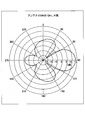
- FIG. 3 is a diagram illustrating an example of directivity on an E-plane of the planar antenna according to the first embodiment. It is a figure showing an example of directivity in the E side of a flat antenna of a 3rd embodiment. It is a figure showing an example of directivity in the H plane of a flat antenna of one comparative form.
- FIG. 3 is a diagram illustrating an example of directivity on an H plane of the planar antenna according to the first embodiment. It is a figure showing an example of directivity in the H plane of the flat antenna of a 3rd embodiment. It is the elements on larger scale in planar view of a planar antenna.
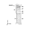
- FIG. 9 shows a perspective view of a planar antenna according to a fourth embodiment.
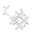
- FIG. 13 shows a perspective view of a planar antenna according to a fifth embodiment.
- a deviation that does not impair the effects of the present invention is allowed in directions such as parallel, right angle, orthogonal, horizontal, vertical, up, down, left, and right.
- the X-axis direction, the Y-axis direction, and the Z-axis direction represent a direction parallel to the X-axis, a direction parallel to the Y-axis, and a direction parallel to the Z-axis, respectively.
- the X-axis direction, the Y-axis direction, and the Z-axis direction are orthogonal to each other.
- the XY plane, the YZ plane, and the ZX plane are a virtual plane parallel to the X-axis direction and the Y-axis direction, a virtual plane parallel to the Y-axis direction and the Z-axis direction, and a virtual plane parallel to the Z-axis direction and the X-axis direction, respectively.
- the planar antenna according to the embodiment of the present disclosure is suitable for transmitting and receiving radio waves in a high frequency band (for example, 0.3 GHz to 300 GHz) such as microwaves and millimeter waves.
- the planar antenna according to the embodiment of the present disclosure is applicable to, for example, a V2X communication system, a fifth-generation mobile communication system (so-called 5G), an in-vehicle radar system, and the like, but applicable systems are not limited to these.
- a V2X communication system is an ETC (Electronic Toll Collection) system.
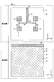
- FIG. 1 is a plan view of the planar antenna according to the first embodiment.
- a planar antenna 101 shown in FIG. 1 includes a dielectric layer 40 through which visible light passes, an antenna conductor 10 provided on one surface of the dielectric layer 40, and a ground conductor 20 opposed to the antenna conductor 10 via the dielectric layer 40. And a power supply line 30 for supplying power to the antenna conductor 10.
- the planar antenna 101 is called a patch antenna or a microstrip antenna.
- FIG. 2 is a plan view of the antenna conductor and the ground conductor of the planar antenna according to the first embodiment.
- the dielectric layer 40 has a first main surface 41 and a second main surface 42 opposite to the first main surface 41. 2 shows the antenna conductor 10 and the feed line 30 provided on the first main surface 41 of the dielectric layer 40. 2 shows the ground conductor 20 provided on the second main surface 42 of the dielectric layer 40.
- the first main surface 41 is an example of a first surface of the dielectric layer.
- the second main surface 42 is an example of a second surface of the dielectric layer opposite to the first surface.
- the dielectric layer 40 is a plate-like or sheet-like base material containing a dielectric as a main component. Both the first main surface 41 and the second main surface 42 are parallel to the XY plane.
- the dielectric layer 40 may be, for example, a dielectric substrate or a dielectric sheet. Examples of the material of the dielectric layer 40 include glass such as quartz glass, ceramics, fluorine-based resin such as polytetrafluoroethylene, liquid crystal polymer, and cycloolefin polymer, but the material is not limited thereto.
- the material of the dielectric layer 40 may be a transparent dielectric member that transmits visible light, and the transparent includes translucent.
- the visible light transmittance of the dielectric layer 40 is preferably, for example, 90% or more from the viewpoint of suppressing the blocking of the visual field.
- the antenna conductor 10 is a planar conductor pattern whose surface is parallel to the XY plane.
- the antenna conductor 10 is a conductor pattern formed on the first main surface 41, and may be formed by a conductor sheet or a conductor substrate disposed on the first main surface 41. Examples of the material of the conductor used for the antenna conductor 10 include, but are not limited to, silver and copper.
- the antenna conductor 10 has, for example, at least one patch conductor.
- the antenna conductor 10 forms an array antenna having four patch conductors 11, 12, 13, and 14.
- the antenna conductor 10 is a solid pattern including a region where the degree of transmission of visible light is lower than that of the dielectric layer 40.
- the entire antenna conductor 10 is formed of an opaque planar conductor including a plurality of patch conductors 11 to 14.
- the power supply line 30 is a planar conductor pattern whose surface is parallel to the XY plane.
- the power supply line 30 is a conductor pattern formed on the first main surface 41, and may be formed by a conductor sheet or a conductor substrate disposed on the first main surface 41. Examples of the material of the conductor used for the power supply line 30 include, but are not limited to, silver and copper.
- the feed line 30 is formed integrally with the antenna conductor 10.
- the power supply line 30 has one end 32 connected to a branch point 36 where a branch path to the patch conductors 11 and 12 and a branch path to the patch conductors 13 and 14 are connected, and an unillustrated external part such as an amplifier. And the other end 33 which is a power supply end connected to the device.
- the feed line 30 is a strip conductor extending in the Y-axis direction, and the end 32 is connected to the antenna conductor 10.
- the power supply line 30 is a solid pattern including a region where the degree of transmission of visible light is lower than that of the dielectric layer 40.
- the entire power supply line 30 is formed of an opaque planar conductor.
- the ground conductor 20 is a conductor pattern whose surface is parallel to the XY plane.
- the ground conductor 20 is a conductor pattern formed on the second main surface 42, and may be formed by a conductor sheet or a conductor substrate disposed on the second main surface 42. Examples of the material of the conductor used for the ground conductor 20 include silver and copper, but are not limited thereto.
- the ground conductor 20 has a linear ground conductor 27 formed so as to have a gap, and a planar ground conductor 26 connected to the linear ground conductor 27.
- the planar ground conductor 26 is a ground portion provided in a band shape on one end side of the second main surface 42.
- the planar ground conductor 26 is a ground electrode corresponding to the end 33 which is a power supply end.
- the linear grounding conductor 27 is formed in a mesh shape so as to form a gap, and the visual field (transparency) can be secured by the gap.
- a lattice-shaped gap is formed.
- the ground conductor 20 includes an outer edge linear conductor 28 that is in contact with the linear ground conductor 27 and forms an outer edge of the ground conductor 20.
- the outer edge linear conductor 28 surrounds the linear ground conductor 27.
- the outer edge linear conductor 28 may be arranged so as to surround a part of the linear ground conductor 27, but the outer edge linear conductor 28 itself need not be arranged. Regarding the presence or absence of the outer edge linear conductor 28, the same applies to the following embodiments.
- the ground conductor 20 is provided in the first region 21 overlapping the antenna conductor 10 and the second region 22 not overlapping the antenna conductor 10 in plan view. More specifically, in the first embodiment, the linear ground conductor 27 is formed in both the first region 21 and the second region 22.
- the second region 22 has a ratio of an area occupied by the ground conductor 20 to an area of ⁇ / 4 ⁇ ⁇ / 4, where ⁇ is an effective wavelength of a radio wave transmitted / received by the planar antenna 101 in the dielectric layer 40 (hereinafter, referred to as ⁇ / 4 ⁇ ⁇ / 4). (Also referred to as a ratio R) of 50% or less.
- ⁇ is an effective wavelength of a radio wave transmitted / received by the planar antenna 101 in the dielectric layer 40
- ⁇ / 4 ⁇ ⁇ / 4 an effective wavelength of a radio wave transmitted / received by the planar antenna 101 in the dielectric layer 40
- the plane antenna 101 when the planar antenna 101 is installed on the surface or inside of the window glass 200, the plane antenna 101 (in particular, the ground conductor 20) has a field of view through the window glass 200 by having the region 23 with the ratio R of 50% or less. Blocking can be suppressed.
- the ratio R is preferably 40% or less, and more preferably 30% or less.
- the lower limit of the ratio R is not particularly limited as long as it is more than 0%, but for ensuring a stable antenna gain, for example, the ratio R may be 2% or more, and is preferably 5% or more.
- the ratio R includes the region 23 of 50% or less and the ratio of the area occupied by the ground conductor 20 to the entire area of the second region 22 (hereinafter, also referred to as ratio R ′) is 50% or less, preferable.
- the ratio R ′ is preferably 40% or less, more preferably 30% or less.
- the lower limit of the ratio R ' is not particularly limited as long as it exceeds 0%.
- the ratio R' may be 2% or more, and is preferably 5% or more.
- the ratio R exceeds 50%, it is difficult to secure a visual field.
- the ratio R is less than 2%, for example, it is easy to secure the visual field, but it is difficult to secure the antenna gain.
- the ratio R ′ exceeds 50%, it is difficult to secure the visual field.
- the ratio R ′ is less than 2%, for example, it is easy to secure the visual field, but it may be difficult to secure the antenna gain.
- FIG. 3 is a plan view of the planar antenna according to the second embodiment.
- the planar antenna 102 shown in FIG. 3 includes a dielectric layer 40 through which visible light passes, an antenna conductor 10 provided on one side of the dielectric layer 40, and a ground conductor 20 facing the antenna conductor 10 via the dielectric layer 40. And a power supply line 30 for supplying power to the antenna conductor 10.
- FIG. 4 is a plan view of the antenna conductor and the ground conductor of the planar antenna according to the second embodiment.
- each of the antenna conductor 10 and the feed line 30 includes a pattern having a region where the degree of transmission of visible light is lower than that of the dielectric layer 40.
- the antenna conductor 10 includes an internal linear conductor 17 formed such that a gap is formed inside the antenna conductor 10.
- the internal linear conductors 17 are formed in a mesh shape so as to form a lattice-shaped gap. At least a portion of the internal linear conductor 17 overlaps with the linear ground conductor 27 of the ground conductor 20 in a plan view, but all of the internal linear conductors 17 overlap with the linear ground conductor 27. More preferred. As described above, since both the antenna conductor 10 and the ground conductor 20 are formed by the linear conductors so as to form a gap, the visual field can be more easily secured.
- the antenna conductor 10 includes the outer linear conductor 18 that is in contact with the inner linear conductor 17 and forms the outer edge of the antenna conductor 10.
- the outer linear conductor 18 is in a closed state surrounding the inner linear conductor 17.
- the outer conductor 18 surrounds the inner conductor 17 in the antenna conductor 10, so that the difference from the current distribution in the case of the planar conductor as in the first embodiment can be suppressed. And good antenna characteristics.
- the power supply line 30 includes an internal linear conductor 37 formed so that a gap is formed inside the power supply line 30.
- the internal linear conductor 37 is formed in a mesh shape so as to form a lattice-shaped gap. At least a portion of the internal linear conductor 37 overlaps with the linear ground conductor 27 of the ground conductor 20 in a plan view, but all of the internal linear conductors 37 overlap with the linear ground conductor 27. More preferred. As described above, since both the power supply line 30 and the ground conductor 20 are formed by the linear conductors so as to form a gap, the visual field can be more easily secured.
- the power supply line 30 includes an outer edge linear conductor 38 that is in contact with the inner linear conductor 37 and forms an outer edge of the power supply line 30.
- the outer linear conductor 38 is in a closed state surrounding the inner linear conductor 37.
- the ground conductor 20 is provided in the first area 21 overlapping the antenna conductor 10 and the second area 22 not overlapping the antenna conductor 10 in plan view.
- the linear ground conductor 27 is formed in both the first region 21 and the second region 22.
- the ratio R of the area occupied by the ground conductor 20 per ⁇ / 4 ⁇ ⁇ / 4 area is 50, where ⁇ is the effective wavelength of the radio wave transmitted and received by the planar antenna 102 in the dielectric layer 40. % Region 23 or less. Therefore, when the second region 22 has such a region 23, the obstruction of the visual field is suppressed, and the planar antenna 102 having excellent directivity and desired transmission / reception sensitivity can be provided.
- the ratio R and the ratio R ' may be values within a preferable range similar to that of the first embodiment. Furthermore, in the case of the second embodiment, it is more preferable that the ratio of the area occupied by the antenna conductor 10 to the entire area of the first region 21 (hereinafter, also referred to as a ratio R ") is 50% or less. Also, like the ratio R, it is preferably 40% or less, and more preferably 30% or less. The lower limit of the ratio R "is not particularly limited as long as it exceeds 0%. However, in order to secure a stable antenna gain, for example, the ratio R" may be 2% or more, and is preferably 5% or more.
- FIG. 5A to 5D are plan views showing other forms of the power supply line 30 in the second embodiment.
- FIG. 5A is a plan view of the power supply line 60a.
- the power supply line 60a has a first power supply line 61 and a second power supply line 62.
- the second power supply line 62 is located between the antenna conductor 10 and the first power supply line 61, and one end is connected to the antenna conductor 10 and the other end is connected to the first power supply line 61.
- the first power supply line 61 has a higher density of conductors per unit area (for example, 1 mm 2 ) than the second power supply line 62 and includes, for example, a part of a solid region having a transmittance of 0% with respect to visible light.
- a configuration may be used, or a configuration in which all of the regions are solid.
- the second power supply line 62 has higher transparency than the first power supply line 61.
- the conductor density of a portion that does not require transparency may be increased to increase the transmission efficiency.
- a conductor density of the portion is higher than other portions.
- the power supply line 60a illustrated in FIG. 5A has a first power supply line 61 and a second power supply line 62 that are adjacent to each other, and includes a boundary line 63 that is a boundary therebetween.
- the first power supply line 61 is a combination in which the entire area is formed of a conductor and the second power supply line 62 has a mesh shape as described above
- the second power supply line 62 has Impedance mismatch occurs and transmission loss easily occurs.
- FIGS. 5A to 5D are plan views showing the feed lines 60a to 60d showing various forms in which impedance mismatch due to the boundary line 63 is suppressed and impedance matching is possible.
- the power supply line 60a shown in FIG. 5A has a configuration in which the width of the first power supply line 61 is constant and the width is smaller than the width of the second power supply line 62.
- the first power supply line 61 has two or more portions having different widths.
- the power supply line 60 b has a first portion 64 including the boundary line 63 and a second portion 65 (not including the boundary line 63), and the width of the first portion 64 is equal to the width of the second power supply line 62. It is smaller than the width and the width of the second portion 65.
- the first portion 64 may be provided so as to function as a transformer whose length in the Y-axis direction is 1 / of the wavelength.
- the design of the impedance transformer becomes easy.
- ⁇ of the wavelength may be, for example, 1 / times the effective wavelength ⁇ when the power supply line 30 is formed on the dielectric layer.
- the width and length (in the Y-axis direction) of the first portion 64 and the width of the second portion 65 can be set to be adjusted to a predetermined impedance.
- the power supply line 60d shown in FIG. 5D has a form in which the width of the first power supply line 61 and the width of the second power supply line 62 are the same, and has two or more portions where the conductor density of the first power supply line 61 is different. is there.
- a first portion 66, a second portion 67, and a third portion 68 are arranged in this order, and the first portion 66 is in contact with the boundary 63.
- the conductor density of the first portion 66 is the lowest, and the conductor density of the second portion 67 and the third portion 68 is lower. Higher configuration.
- the power supply line 30 in the second embodiment is not limited to the power supply lines 60a to 60d shown in FIGS. 5A to 5D, and can be appropriately adjusted to a conductor density so as to enable impedance matching.
- the shape can be appropriately adjusted to a combination of the forms.
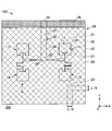
- FIG. 6 is a plan view of the antenna conductor and the ground conductor of the planar antenna according to the third embodiment. 6 includes a dielectric layer 40 through which visible light passes, an antenna conductor 10 provided on one surface of the dielectric layer 40, and a ground conductor 20 facing the antenna conductor 10 via the dielectric layer 40. And a power supply line 30 for supplying power to the antenna conductor 10.
- planar antenna 103 of the third embodiment shown in FIG. 6 looks like the same shape shown in FIG. 1 in plan view.
- the form of the ground conductor 20 is different from that of the first embodiment shown in FIG.
- the ground conductor 20 includes a planar ground conductor 25 entirely overlapping the antenna conductor 10 in plan view. Since the planar antenna conductor 10 and the planar ground conductor 25 face each other, the level of the ground portion as the planar ground conductor 25 is stabilized. Furthermore, since the planar antenna conductor 10 and the planar ground conductor 25 are opposed to each other, the planar ground conductor 25 is located on the back side of the patch serving as a main radiation source (the planar antenna conductor 10). Therefore, since the planar ground conductor 25 functions as a reflector, the directivity and antenna gain on the front side (+ Z side) of the patch can be improved. In the third embodiment, the planar ground conductor 25 has the same shape as the antenna conductor 10 in plan view.
- the planar ground conductor 25 may partially overlap the antenna conductor 10 so that a part of the planar ground conductor 25 protrudes from the antenna conductor 10 in a plan view, The part may overlap the antenna conductor 10 so that the part is inside the outer edge of the antenna conductor 10.
- the grounding conductor 20 includes a planar grounding conductor 29 that entirely overlaps the power supply line 30 in plan view. Since the planar power supply line 30 and the planar ground conductor 29 face each other, the operation as the power supply line is stabilized. In the third embodiment, the planar ground conductor 29 has the same shape as the power supply line 30 in plan view. Thereby, it is easy to secure the visual field.
- the planar ground conductor 29 may overlap with the power supply line 30 so that a part of the planar ground conductor 29 protrudes from the power supply line 30 in a plan view.
- the power supply line 30 may partially overlap the power supply line 30 so that the power supply line 30 is partially inside the outer edge of the power supply line 30.
- FIG. 7 is a plan view of a plurality of linear conductors crossing each other.
- the line width W of the linear ground conductor 27 is preferably from 1 to 500 ⁇ m from the viewpoint of securing a visual field. If the line width W is less than 1 ⁇ m, the antenna gain may not be stable because the ground (earth) is not stabilized. If the line width W exceeds 500 ⁇ m, it is difficult to secure a visual field. Therefore, when the line width W is 1 to 500 ⁇ m, both stable antenna gain and a sufficient field of view can be ensured. Further, the line width W is preferably from 3 to 200 ⁇ m, more preferably from 5 to 50 ⁇ m.
- the linear ground conductor 27 includes a first linear ground conductor extending in the first linear direction 51 and a second linear ground conductor extending in a second linear direction 52 orthogonal to the first linear direction 51. .
- the ground is stabilized, and variations in antenna characteristics can be suppressed.
- FIG. 7 shows a state in which two first linear ground conductors and two second linear ground conductors intersect.
- the line width W of the linear ground conductor 27 is preferably 0.5 to 30% with respect to the pitch P1 (or the pitch P2) from the viewpoint of securing a visual field. If the line width W is less than 0.5% with respect to the pitch P1 or the pitch P2, the antenna gain may not be stable because the ground (earth) is not stabilized. If the line width W is more than 30% of the pitch P1 or the pitch P2, it is difficult to secure a visual field.
- the line width W is 0.5 to 30% with respect to the pitch P1 (or the pitch P2), it is possible to achieve both a stable antenna gain and a secure view. Further, the line width W is preferably 0.7% to 23% with respect to the pitch P1 (or the pitch P2), and more preferably 1% to 15%.
- the length L of the outer edge of the region 53 surrounded by the linear ground conductor 27 is preferably 1 ⁇ or less with respect to the effective wavelength ⁇ of the dielectric layer 40, from the viewpoint of improving the antenna gain. If the length L exceeds 1 ⁇ , unnecessary resonance occurs in the linear ground conductor, and it becomes difficult to secure antenna performance.
- FIG. 8 is a plan view of a planar antenna according to a comparative example. 8 includes a dielectric layer 40 through which visible light is transmitted, an antenna conductor 110 provided on one surface of the dielectric layer 40, and a ground conductor 120 facing the antenna conductor 110 via the dielectric layer 40. And a power supply line 130 for supplying power to the antenna conductor 110. 8, the form of the ground conductor is different from that of the first embodiment shown in FIGS.
- the ground conductor 120 shown in FIG. 8 is a solid pattern composed of a region where the degree of transmission of visible light is lower than that of the dielectric layer 40.
- the whole ground conductor 120 is formed of an opaque planar conductor.
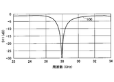
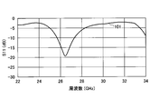
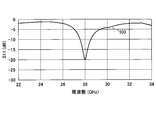
- FIG. 9 is a diagram illustrating an example of the return loss characteristic of the planar antenna 100 according to the comparative example.
- FIG. 10 is a diagram illustrating an example of the return loss characteristics of the planar antenna 101 according to the first embodiment.
- FIG. 11 is a diagram illustrating an example of a return loss characteristic of the planar antenna 103 according to the third embodiment. 9 to 11, S11 on the vertical axis indicates a return loss characteristic.
- the planar antennas 101 and 103 of this embodiment have sufficient return loss characteristics.
- the field of view is blocked because the ground conductor 120 is a planar conductor. Therefore, the planar antennas 101 and 103 of the present embodiment can obtain a sufficient return loss characteristic while suppressing the obstruction of the field of view.
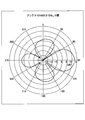
- FIGS. 12 to 14 are diagrams showing examples of directivity on the E plane of the planar antennas 100, 101, and 103, respectively.
- 15 to 17 are diagrams illustrating examples of directivity on the H plane of the planar antennas 100, 101, and 103, respectively.
- the E plane represents a YZ plane passing through the branch point 36
- the H plane represents a ZX plane passing through the branch point 36.
- the planar antennas 101 and 103 of the present embodiment can obtain the same antenna gain and the same directivity as the planar antenna 100. Therefore, the planar antennas 101 and 103 of the present embodiment have excellent directivity and have desired transmission / reception sensitivity while suppressing obstruction of the field of view.
- the planar antenna 101 of the first embodiment has high transmission / reception sensitivity to radio waves of 26.5 GHz.
- the ratio (R) of the area occupied by the ground conductor 20 per area of ⁇ ⁇ / 4 was set to 20%.
- the pitch P2 between the adjacent first linear ground conductors and the pitch P1 between the adjacent second linear ground conductors are equal to each other, that is, 847 ⁇ m.
- the line width W was 100 ⁇ m, and the ratio of the line width W to the pitches P1 and P2 was 12%.
- the planar antenna 103 according to the third embodiment has high transmission / reception sensitivity to radio waves of 28 GHz, and the second main surface 42 has ⁇ / 4 ⁇ ⁇
- the ratio (R) of the area occupied by the ground conductor 20 per ⁇ area was set to 20%.
- the pitch P2 between the adjacent first linear ground conductors and the pitch P1 between the adjacent second linear ground conductors are equal to each other, that is, 847 ⁇ m.
- the line width W was 100 ⁇ m, and the ratio of the line width W to the pitches P1 and P2 was 12%.
- the planar antenna 100 of the comparative example has high transmission / reception sensitivity to radio waves of 28 GHz in the examples shown in FIGS. 9, 12 and 15, and the second main surface 42 has ⁇ / 4 ⁇ ⁇ / 4.
- the ratio (R) of the area occupied by the ground conductor 20 per area is 100%.
- planar antennas 100, 101, and 103 of the examples shown in FIGS. 9 to 17 the common dimensions of the respective parts are as shown in FIG.
- planar antenna and the window glass have been described above with reference to the embodiments, the present invention is not limited to the above embodiments. Various modifications and improvements, such as combinations and substitutions with some or all of the other embodiments, are possible within the scope of the present invention.
- the antenna conductor may have a lower or higher visible light transmission degree than the dielectric layer, or may have the same transmittance as the dielectric layer. Further, the linear conductor may be formed in a mesh shape so as to form a gap, or may be formed in a stripe shape so as to form a gap.
- the outer shape of the antenna conductor may be another shape such as a circle. Further, the antenna conductor may be fed by another feeding line such as a feeding pin or a through hole.
- FIG. 19 is a perspective view of the planar antenna according to the fourth embodiment in which the feed line 30 is configured by a coplanar line.
- the planar antenna 104 includes a dielectric layer 40 through which visible light passes, an antenna conductor 10 provided on one surface of the dielectric layer 40, a ground conductor 20 opposed to the antenna conductor 10 via the dielectric layer 40, 10 is provided with a power supply line 30 for supplying power via a slot 31.
- the feed line 30 and the ground conductor 20 are formed on the second main surface of the dielectric layer 40 (the surface opposite to the first main surface 41 on which the antenna conductor 10 is formed).
- the power supply line 30 has a pair of gaps running in parallel and a center conductor sandwiched between the pair of gaps.
- the slot 31 formed at one end of the feed line 30 and the antenna conductor 10 formed on the first main surface 41 are coupled at a high frequency.
- the ground conductor 20 has a linear ground conductor 27 formed so as to form a gap, and the linear ground conductor 27 is formed in a mesh shape so as to form a gap.
- the view (transparency) can be secured.
- at least one of the center conductor of the power supply line 30 and the antenna conductor 10 may have a linear conductor formed so as to form a gap. Thereby, further transparency can be secured.
- FIG. 20 is a perspective view of the planar antenna according to the fifth embodiment. Description of the same configuration and effect as the fifth embodiment will be omitted by using the description of the above embodiment.
- the planar antenna 105 includes dielectric layers 40A and 40B through which visible light passes, an antenna conductor 10 provided on one surface of the dielectric layer 40A, and a ground conductor 20 facing the antenna conductor 10 via the dielectric layer 40A. A feed line 30 for feeding power to the antenna conductor 10 via the slot 31;
- the ground conductor 20 is sandwiched between a pair of dielectric layers 40A and 40B.
- the antenna conductor 10 is a patch conductor formed on the surface of the first dielectric layer 40A.
- the power supply line 30 is a microstrip line formed on the surface of the second dielectric layer 40B.
- the antenna conductor 10 is fed and excited by electromagnetic coupling between the antenna conductor 10 and the feed line 30 via the slot 31 provided in the ground conductor 20.
- the ground conductor 20 shown in FIG. 20 has a linear ground conductor formed so as to form a gap.
- a visual field (transparency) can be secured by the gap.
- at least one of the power supply line 30 and the antenna conductor 10 may have a linear conductor formed so as to form a gap. Thereby, further transparency can be secured.
Abstract
第1面と、前記第1面とは反対側の第2面とを有し、可視光が透過する誘電体層と、前記第1面に設けられるアンテナ導体と、前記第2面に設けられる接地導体とを備え、前記接地導体は、平面視において、前記アンテナ導体と重複する第1領域と、前記アンテナ導体と重複しない第2領域に配置され、前記第2領域は、平面アンテナによって送受される電波の、前記誘電体層における実効波長をλとすると、λ/4×λ/4の面積あたりに前記接地導体が占める面積の割合が50%以下の領域を有する、平面アンテナ。
Description
本発明は、平面アンテナ及び窓ガラスに関する。
近年、4G LTEから5G(sub6)への移行など、マイクロ波やミリ波の周波数帯を使用する高速・大容量の無線通信システムを利用するサービスが拡がる動きがある。具体的には、3GHz帯域から5~6GHz帯域まで、そのようなサービスの使用帯域が広がる傾向にある。更に高周波の28GHz帯なども有望な帯域と期待されている。このような周波数帯に対応可能であって、指向性及び受信感度の良好なアンテナとして、パッチアンテナに代表される平面アンテナが知られており、様々な平面形状を有する平面アンテナが開示されている(例えば、特許文献1,2参照)。
ところが、従来のパッチアンテナは、所定の形状を有するパッチアンテナ部分と、パッチアンテナ部分に誘電体基板を介して対向する金属箔から形成される接地導体とを有するため、可視光の透過がその接地導体によって遮られる。したがって、従来の技術では、パッチアンテナを例えば窓ガラスなどの可視光透過部材に取り付けた場合、パッチアンテナ(特に、接地導体)が窓ガラス越しの視野を遮ってしまう問題があった。
そこで、本開示は、視野の遮りを抑え、指向性に優れ、所望の送受感度を有する平面アンテナを提供するとともに、少なくとも一つの当該平面アンテナを備える窓ガラスを提供する。
本開示は、
第1面と、前記第1面とは反対側の第2面とを有し、可視光が透過する誘電体層と、
前記第1面に設けられるアンテナ導体と、
前記第2面に設けられる接地導体とを備え、
前記接地導体は、平面視において、前記アンテナ導体と重複する第1領域と、前記アンテナ導体と重複しない第2領域に配置され、
前記第2領域は、平面アンテナによって送受される電波の、前記誘電体層における実効波長をλとすると、λ/4×λ/4の面積あたりに前記接地導体が占める面積の割合が50%以下の領域を有する、平面アンテナを提供する。
第1面と、前記第1面とは反対側の第2面とを有し、可視光が透過する誘電体層と、
前記第1面に設けられるアンテナ導体と、
前記第2面に設けられる接地導体とを備え、
前記接地導体は、平面視において、前記アンテナ導体と重複する第1領域と、前記アンテナ導体と重複しない第2領域に配置され、
前記第2領域は、平面アンテナによって送受される電波の、前記誘電体層における実効波長をλとすると、λ/4×λ/4の面積あたりに前記接地導体が占める面積の割合が50%以下の領域を有する、平面アンテナを提供する。
また、本開示は、少なくとも一つの当該平面アンテナを備える窓ガラスを提供する。
本開示の技術によれば、視野の遮りを抑え、指向性に優れ、所望の送受感度を有する平面アンテナ、及び、少なくとも一つの当該平面アンテナを備える窓ガラスを提供できる。
以下、図面を参照して、本開示に係る実施形態の説明を行う。なお、各形態において、平行、直角、直交、水平、垂直、上下、左右などの方向には、本発明の効果を損なわない程度のずれが許容される。また、X軸方向、Y軸方向、Z軸方向は、それぞれ、X軸に平行な方向、Y軸に平行な方向、Z軸に平行な方向を表す。X軸方向とY軸方向とZ軸方向は、互いに直交する。XY平面、YZ平面、ZX平面は、それぞれ、X軸方向及びY軸方向に平行な仮想平面、Y軸方向及びZ軸方向に平行な仮想平面、Z軸方向及びX軸方向に平行な仮想平面を表す。
本開示に係る実施形態の平面アンテナは、マイクロ波やミリ波等の高周波帯(例えば、0.3GHz~300GHz)の電波の送受に好適である。本開示に係る実施形態の平面アンテナは、例えば、V2X通信システム、第5世代移動通信システム(いわゆる、5G)、車載レーダーシステムなどに適用可能であるが、適用可能なシステムはこれらに限られない。V2X通信システムの一例として、ETC(Electronic Toll Collection)システムがある。
図1は、第1の実施形態の平面アンテナの平面図である。図1に示す平面アンテナ101は、可視光が透過する誘電体層40と、誘電体層40の片面に設けられるアンテナ導体10と、誘電体層40を介してアンテナ導体10と対向する接地導体20と、アンテナ導体10に給電する給電ライン30とを備える。平面アンテナ101は、パッチアンテナ又はマイクロストリップアンテナと称される。
図2は、第1の実施形態の平面アンテナのアンテナ導体及び接地導体の平面図である。誘電体層40は、第1主面41と、第1主面41とは反対側の第2主面42とを有する。図2の上段は、誘電体層40の第1主面41に設けられるアンテナ導体10及び給電ライン30を示す。図2の下段は、誘電体層40の第2主面42に設けられる接地導体20を示す。第1主面41は、誘電体層の第1面の一例である。第2主面42は、誘電体層の第1面とは反対側の第2面の一例である。
誘電体層40は、誘電体を主成分とする板状又はシート状の基材である。第1主面41及び第2主面42は、いずれも、XY平面に平行である。誘電体層40は、例えば、誘電体基板でもよいし、誘電体シートでもよい。誘電体層40の材料は、例えば、石英ガラス等のガラス、セラミックス、ポリテトラフルオロエチレン等のフッ素系樹脂、液晶ポリマー、シクロオレフィンポリマーなどが挙げられるが、その材料は、これらに限られない。
また、誘電体層40の材料は、可視光が透過する透明な誘電体部材であればよく、透明には、半透明が含まれる。誘電体層40の可視光線透過率は、視野の遮りを抑える点で、例えば90%以上が好ましい。
アンテナ導体10は、その表面がXY平面に平行な平面状の導体パターンである。アンテナ導体10は、第1主面41に形成される導体パターンであり、第1主面41に配置される導体シート又は導体基板により形成されてもよい。アンテナ導体10に使用される導体の材料として、例えば、銀、銅などが挙げられるが、これらに限られない。
アンテナ導体10は、例えば、少なくとも一つのパッチ導体を有する。第1の実施形態では、アンテナ導体10は、4つのパッチ導体11,12,13,14を有するアレイアンテナを構成する例を示す。
第1の実施形態では、アンテナ導体10は、可視光の透過度合いが誘電体層40よりも低い領域から構成されたソリッドなパターンである。例えば、アンテナ導体10の全体は、複数のパッチ導体11~14を含め、不透明な面状導体から構成されている。
給電ライン30は、その表面がXY平面に平行な平面状の導体パターンである。給電ライン30は、第1主面41に形成される導体パターンであり、第1主面41に配置される導体シート又は導体基板により形成されてもよい。給電ライン30に使用される導体の材料として、例えば、銀、銅などが挙げられるが、これらに限られない。第1の実施形態では、給電ライン30は、アンテナ導体10と一体的に形成されている。
給電ライン30は、パッチ導体11,12への分岐路とパッチ導体13,14への分岐路とが接続される分岐箇所36に接続される一方の端部32と、アンプ等の不図示の外部装置に接続される給電端である他方の端部33とを有する。第1の実施形態では、給電ライン30は、Y軸方向に延伸するストリップ導体であり、端部32がアンテナ導体10に接続されている。
第1の実施形態では、給電ライン30は、可視光の透過度合いが誘電体層40よりも低い領域から構成されたソリッドなパターンである。例えば、給電ライン30の全体は、不透明な面状導体から構成されている。
接地導体20は、その表面がXY平面に平行な導体パターンである。接地導体20は、第2主面42に形成される導体パターンであり、第2主面42に配置される導体シート又は導体基板により形成されてもよい。接地導体20に使用される導体の材料として、例えば、銀、銅などが挙げられるが、これらに限られない。
接地導体20は、隙間が生じるように形成される線状接地導体27と、線状接地導体27に接続される面状接地導体26とを有する。面状接地導体26は、第2主面42の一端辺に帯状に設けられたグランド部である。面状接地導体26は、給電端である端部33に対応するグランド電極である。
第1の実施形態では、線状接地導体27は、隙間が生じるように網目状に形成され、当該隙間によって視野(透明性)を確保できる。第1の実施形態では、格子状の隙間が形成されている。
第1の実施形態では、接地導体20は、線状接地導体27と接し、接地導体20の外縁を形成する外縁線状導体28を含む。外縁線状導体28は、線状接地導体27を囲んでいる。なお、外縁線状導体28は、線状接地導体27の一部を囲むように配置されてもよいが、外縁線状導体28自体を配置しなくてもよい。外縁線状導体28配置の有無については、以下の実施形態も同様である。
第1の実施形態では、図1に示されるように、平面視において、アンテナ導体10と重複する第1領域21と、アンテナ導体10と重複しない第2領域22に接地導体20を有する。より具体的に、第1の実施形態では、線状接地導体27が第1領域21と第2領域22の両方に形成されている。
第2領域22は、平面アンテナ101によって送受される電波の、誘電体層40における実効波長をλとすると、λ/4×λ/4の面積あたりに接地導体20が占める面積の割合(以下、割合Rとも称する)が50%以下の領域23を有する。第1の実施形態では、領域23は、可視光の透過を遮る線状接地導体27の割合Rが50%以下である。第2領域22がこのような領域23を有することにより、視野の遮りを抑え、指向性に優れ、所望の送受感度を有する平面アンテナ101を提供できる。例えば、平面アンテナ101を窓ガラス200の表面又は内部に設置した場合、割合Rが50%以下の領域23を有することにより、平面アンテナ101(特に、接地導体20)が窓ガラス200越しの視野を遮ることを抑制できる。割合Rは、40%以下が好ましく、30%以下がより好ましい。割合Rの下限は、0%超であればとくに制限されないが、安定したアンテナ利得を確保するために例えば、割合Rは、2%以上であればよく、5%以上であれば好ましい。また、割合Rが50%以下の領域23を有するとともに、第2領域22全ての面積あたりに接地導体20が占める面積の割合(以下、割合R'とも称する)が50%以下であると、より好ましい。割合R'も、割合Rと同様に、40%以下が好ましく、30%以下がより好ましい。割合R'の下限は、0%超であればとくに制限されないが、安定したアンテナ利得を確保するために例えば、割合R'は、2%以上であればよく、5%以上であれば好ましい。
割合Rが50%を超えると、視野の確保が難しくなる。割合Rが例えば2%未満になると、視野の確保が容易になるが、アンテナ利得の確保が難しくなる。また、割合R'が50%を超えると、視野の確保が難しくなり、割合R'が例えば2%未満になると、視野の確保が容易になるが、アンテナ利得の確保が難しくなる場合がある。
図3は、第2の実施形態の平面アンテナの平面図である。図3に示す平面アンテナ102は、可視光が透過する誘電体層40と、誘電体層40の片面に設けられるアンテナ導体10と、誘電体層40を介してアンテナ導体10と対向する接地導体20と、アンテナ導体10に給電する給電ライン30とを備える。
第1の実施形態と同様の構成及び効果についての説明は、上述の実施形態の説明を援用することで省略する。図3に示す第2の実施形態では、アンテナ導体10及び給電ライン30の形態が、図1に示す第1の実施形態と異なる。
図4は、第2の実施形態の平面アンテナのアンテナ導体及び接地導体の平面図である。第2の実施形態では、アンテナ導体10及び給電ライン30は、いずれも、可視光の透過度合いが誘電体層40よりも低い領域を有するパターンを含む。
アンテナ導体10は、隙間がアンテナ導体10の内部に生じるように形成される内部線状導体17を含む。第2の実施形態では、内部線状導体17は、格子状の隙間が生じるように網目状に形成されている。内部線状導体17の少なくとも一部は、平面視において、接地導体20の線状接地導体27と重複しているが、内部線状導体17の全てが線状接地導体27と重複しているとより好ましい。このように、アンテナ導体10と接地導体20の両方が、隙間が生じるように線状導体によって形成されているので、視野の確保が更に容易になる。
第2の実施形態では、アンテナ導体10は、内部線状導体17と接し、アンテナ導体10の外縁を形成する外縁線状導体18を含む。外縁線状導体18は、内部線状導体17を囲んで閉じた状態になっている。このように、アンテナ導体10について、外縁線状導体18が内部線状導体17を囲む構成とすることで、第1の実施形態のような面状導体の場合の電流分布との相違を抑制でき、良好なアンテナ特性を確保できる。
給電ライン30は、隙間が給電ライン30の内部に生じるように形成される内部線状導体37を含む。第2の実施形態では、内部線状導体37は、格子状の隙間が生じるように網目状に形成されている。内部線状導体37の少なくとも一部は、平面視において、接地導体20の線状接地導体27と重複しているが、内部線状導体37の全てが線状接地導体27と重複しているとより好ましい。このように、給電ライン30と接地導体20の両方が、隙間が生じるように線状導体によって形成されているので、視野の確保が更に容易になる。
第2の実施形態では、給電ライン30は、内部線状導体37と接し、給電ライン30の外縁を形成する外縁線状導体38を含む。外縁線状導体38は、内部線状導体37を囲んで閉じた状態になっている。このように、給電ライン30について、外縁線状導体38が内部線状導体37を囲む構成とすることで、第1の実施形態のような面状導体の場合の電流分布との相違を抑制でき、良好なアンテナ特性を確保できる。
第2の実施形態でも、図3に示されるように、平面視において、アンテナ導体10と重複する第1領域21と、アンテナ導体10と重複しない第2領域22に接地導体20を有する。第2の実施形態では、線状接地導体27が第1領域21と第2領域22の両方に形成されている。第2領域22は、平面アンテナ102によって送受される電波の、誘電体層40における実効波長をλとすると、λ/4×λ/4の面積あたりに接地導体20が占める面積の割合Rが50%以下の領域23を有する。したがって、第2領域22がこのような領域23を有することにより、視野の遮りを抑え、指向性に優れ、所望の送受感度を有する平面アンテナ102を提供できる。なお、割合R、割合R'は、第1の実施形態と同じような好ましい範囲の値であればよい。さらに、第2の実施形態の場合、第1領域21全ての面積あたりにアンテナ導体10が占める面積の割合(以下、割合R"とも称する)が50%以下であると、より好ましい。割合R"も、割合Rと同様に、40%以下が好ましく、30%以下がより好ましい。割合R"の下限は、0%超であればとくに制限されないが、安定したアンテナ利得を確保するために例えば、割合R"は、2%以上であればよく、5%以上であれば好ましい。
図5A~図5Dは、第2の実施形態における給電ライン30の他の形態を示す平面図である。図5Aは、給電ライン60aの平面図であり、給電ライン60aは、第1の給電ライン61と第2の給電ライン62を有する。第2の給電ライン62は、アンテナ導体10と第1の給電ライン61との間に位置し、一端はアンテナ導体10に接続され、他端は第1の給電ライン61に接続される。第1の給電ライン61は、単位面積(例えば1mm2)あたりの導体の密度が、第2の給電ライン62よりも高く、例えば可視光に対する透過率が0%であるソリッドな領域を一部含む構成でもよく、全てがソリッドな領域からなる構成でもよい。言い換えると、第2の給電ライン62は、第1の給電ライン61よりも高い透明性を有する。とくに、給電ライン60a(30)は、伝送線路が長くなるほど伝送損失が大きくなるため、例えば、透明性を必要としない部分の導体密度を高くして伝送効率を高めてもよい。例えば、第1領域21に至るまでの給電ラインのうち、第1領域21から離れる部分ほど、透明性を必要としない場合があり、該部分の導体密度を他の部分よりも高くする構成が挙げられる。
図5Aに示す給電ライン60aは、互いに隣り合う第1の給電ライン61と第2の給電ライン62とを有し、これらの境界となる境界線63を含む。例えば、第1の給電ライン61はその領域が全て導体によって形成され、第2の給電ライン62はその領域が上述のような網目状となっている組み合わせの場合、境界線63で給電ライン60aのインピーダンス不整合が発生して伝送損失が生じやすくなる。図5A~図5Dは、境界線63によるインピーダンス不整合を抑制し、インピーダンス整合が可能となるような種々の形態を示した、給電ライン60a~給電ライン60dを示した平面図である。
図5Aに示す給電ライン60aは、第1の給電ライン61の幅が一定で、その幅が第2の給電ライン62の幅よりも狭い形態である。図5Bに示す給電ライン60bは、第1の給電ラインの61が、異なる幅を有する2つ以上の部分を有する。例えば、給電ライン60bは、境界線63を含む第1の部分64と(境界線63を含まない)第2の部分65を有し、第1の部分64の幅は第2の給電ライン62の幅および第2の部分65の幅よりも狭い。第1の部分64は、そのY軸方向の長さが、波長の1/4となる変成器として機能するように設けてよい。インピーダンス変成器の長さを波長の1/4とすることで、インピーダンス変成器の設計が容易になる。なお、「波長の1/4」とは、例えば給電ライン30が誘電体層上に形成されている場合、実効波長λの1/4倍とするとよい。このようにして、第1の部分64の幅および(Y軸方向の)長さ、ならびに第2の部分65の幅は、所定のインピーダンスに調整するよう設定できる。
図5Cに示す給電ライン60cは、第1の給電ライン61の幅が境界線63に近くなるにつれて狭くなる形態である。第1の給電ライン61は、その長手方向に沿った外縁が直線に限らず曲線を含む形状でもよい。図5Dに示す給電ライン60dは、第1の給電ライン61の幅と第2の給電ライン62の幅が同一で、第1の給電ライン61の導体密度が異なる2つ以上の部分を有する形態である。例えば、給電ライン60dは、第1の部分66、第2の部分67、第3の部分68がこの順に並んで配置され、第1の部分66は、境界線63と接する。例えば、第1の部分66、第2の部分67および第3の部分68のうち、第1の部分66の導体密度が最も低く、第2の部分67、第3の部分68の順に導体密度が高くなる構成が挙げられる。
なお、第2の実施形態における給電ライン30は、図5A~図5Dに示した給電ライン60a~給電ライン60dに限らず、インピーダンス整合が可能となるように、導体密度に適宜調整でき、これらの形態を組み合わせた形状に適宜調整できる。
図6は、第3の実施形態の平面アンテナのアンテナ導体及び接地導体の平面図である。図6に示す平面アンテナ103は、可視光が透過する誘電体層40と、誘電体層40の片面に設けられるアンテナ導体10と、誘電体層40を介してアンテナ導体10と対向する接地導体20と、アンテナ導体10に給電する給電ライン30とを備える。
第3の実施形態と同様の構成及び効果についての説明は、上述の実施形態の説明を援用することで省略する。図6に示す第3の実施形態の平面アンテナ103は、平面視で、図1に示す同じ形状に見える。第3の実施形態では、接地導体20の形態が、図1に示す第1の実施形態と異なる。
接地導体20は、平面視において、全体がアンテナ導体10と重複する面状接地導体25を含む。面状のアンテナ導体10と面状接地導体25とが対向しているので、面状接地導体25としてのグランド部のレベルが安定する。さらに、面状のアンテナ導体10と面状接地導体25とが対向していることで、面状接地導体25が主な放射源(面状のアンテナ導体10)となるパッチの裏側に位置する。そのため、面状接地導体25が反射板として機能するため、パッチの表側(+Z側)の指向性やアンテナ利得の向上が可能となる。第3の実施形態では、面状接地導体25は、平面視において、アンテナ導体10と同形状である。これにより、視野の確保が容易になる。なお、面状接地導体25は、平面視において、面状接地導体25の一部がアンテナ導体10からはみ出るように、当該一部がアンテナ導体10と重複してもよく、面状接地導体25の一部がアンテナ導体10の外縁よりも内側となるように、当該一部がアンテナ導体10と重複してもよい。
接地導体20は、平面視において、全体が給電ライン30と重複する面状接地導体29を含む。面状の給電ライン30と面状接地導体29とが対向しているので、給電ラインとしての動作が安定する。第3の実施形態では、面状接地導体29は、平面視において、給電ライン30と同形状である。これにより、視野の確保が容易になる。なお、面状接地導体29は、平面視において、面状接地導体29の一部が給電ライン30からはみ出るように、当該一部が給電ライン30と重複してもよく、面状接地導体29の一部が給電ラインの30の外縁よりも内側になるように、当該一部が給電ライン30と重複してもよい。
図7は、相互に交差する複数の線状導体の平面図である。線状接地導体27の線幅Wは、1~500μmであることが、視野の確保の点で好ましい。線幅Wが1μm未満であると、接地(アース)が安定せずにアンテナ利得が安定しなくなるおそれがある。また、線幅Wが500μm超であると、視野の確保が難しくなる。したがって、線幅Wが1~500μmであると、安定したアンテナ利得と視野の確保が両立できる。また、線幅Wは、3~200μmが好ましく、5~50μmがより好ましい。
また、線状接地導体27は、第1直線方向51に延伸する第1線状接地導体と、第1直線方向51と直交する第2直線方向52に延伸する第2線状接地導体とを含む。これにより、接地(アース)が安定しアンテナ特性のばらつきを抑制できる。図7は、2本の第1線状接地導体と2本の第2線状接地導体とが交差している状態を示している。
隣り合う第1線状接地導体の間のピッチP2と、隣り合う第2線状接地導体の間のピッチP1と、が等しいと、アンテナの指向性のばらつきを抑制できる。線状接地導体27の線幅Wは、ピッチP1(又は、ピッチP2)に対して0.5~30%であることが、視野の確保の点で好ましい。線幅WがピッチP1又はピッチP2に対して0.5%未満であると、接地(アース)が安定せずにアンテナ利得が安定しなくなるおそれがある。また、線幅WがピッチP1又はピッチP2に対して30%超であると、視野の確保が難しくなる。したがって、線幅Wは、ピッチP1(又は、ピッチP2)に対して0.5~30%であると、安定したアンテナ利得と視野の確保が両立できる。また、線幅Wは、ピッチP1(又は、ピッチP2)に対して0.7~23%が好ましく、1~15%がより好ましい。
また、線状接地導体27に囲まれる領域53の外縁の長さLは、誘電体層40における実効波長λに対して、1λ以下であることが、アンテナ利得を向上させる点で好ましい。長さLが1λを超えると、線状接地導体で不要な共振が発生しアンテナ性能の確保が難しくなる。
次に、本実施形態の平面アンテナのリターンロスと指向性を、一比較形態の平面アンテナと比較した結果について説明する。
図8は、一比較形態の平面アンテナの平面図である。図8に示す平面アンテナ100は、可視光が透過する誘電体層40と、誘電体層40の片面に設けられるアンテナ導体110と、誘電体層40を介してアンテナ導体110と対向する接地導体120と、アンテナ導体110に給電する給電ライン130とを備える。図8に示す形態では、接地導体の形態が、図1,2に示す第1の実施形態と異なる。
図8に示す接地導体120は、可視光の透過度合いが誘電体層40よりも低い領域から構成されたソリッドなパターンである。接地導体120の全体は、不透明な面状導体から構成されている。
図9は、一比較形態の平面アンテナ100のリターンロス特性の一例を示す図である。図10は、第1の実施形態の平面アンテナ101のリターンロス特性の一例を示す図である。図11は、第3の実施形態の平面アンテナ103のリターンロス特性の一例を示す図である。図9~11において、縦軸のS11は、リターンロス特性を示す。
図10,11に示されるように、本実施形態の平面アンテナ101,103は十分なリターンロス特性が得られる。一方、平面アンテナ100は、接地導体120が面状導体であるため、視界が遮られる。したがって、本実施形態の平面アンテナ101,103は、視界の遮りを抑制しつつ、十分なリターンロス特性が得られる。
図12~14は、それぞれ、平面アンテナ100,101,103のE面での指向性の一例を示す図である。図15~17は、それぞれ、平面アンテナ100,101,103のH面での指向性の一例を示す図である。E面は、分岐箇所36を通るYZ平面を表し、H面は、分岐箇所36を通るZX平面を表す。図12~17に示されるように、本実施形態の平面アンテナ101,103は、平面アンテナ100と同等のアンテナ利得と同等の指向性が得られる。したがって、本実施形態の平面アンテナ101,103は、視界の遮りを抑制しつつ、指向性に優れ、所望の送受感度を有する。
なお、第1の実施形態の平面アンテナ101は、図10,13,16に示す例では、26.5GHzの電波に対して高い送受感度を示すものあり、第2主面42において、λ/4×λ/4の面積あたりに接地導体20が占める面積の割合(R)は、20%とした。また、隣り合う第1線状接地導体の間のピッチP2と、隣り合う第2線状接地導体の間のピッチP1と、が等しく、847μmとした。また、線幅Wは100μmであり、ピッチP1,P2に対する線幅Wの割合は12%であった。
また、第3の実施形態の平面アンテナ103は、図11,14,17に示す例では、28GHzの電波に対して高い送受感度を示すものあり、第2主面42において、λ/4×λ/4の面積あたりに接地導体20が占める面積の割合(R)は、20%とした。また、隣り合う第1線状接地導体の間のピッチP2と、隣り合う第2線状接地導体の間のピッチP1と、が等しく、847μmとした。また、線幅Wは100μmであり、ピッチP1,P2に対する線幅Wの割合は12%であった。
また、一比較形態の平面アンテナ100は、図9,12,15に示す例では、28GHzの電波に対して高い送受感度を示すものあり、第2主面42において、λ/4×λ/4の面積あたりに接地導体20が占める面積の割合(R)は、100%である。
また、図9~17に示す例の平面アンテナ100,101,103において、図1に示す共通寸法L11,L12,L13は、単位をmmとすると、
L11:18
L12:18
L13:1.1
である。
L11:18
L12:18
L13:1.1
である。
また、図9~17に示す例の平面アンテナ100,101,103において、各部の共通寸法は、図18に示す通りである。
以上、平面アンテナ及び窓ガラスを実施形態により説明したが、本発明は上記の実施形態に限定されるものではない。他の実施形態の一部又は全部との組み合わせや置換などの種々の変形及び改良が、本発明の範囲内で可能である。
アンテナ導体は、可視光の透過度合いが、誘電体層に比べて低く又は高くてもよく、誘電体層と同じでもよい。また、線状導体は、隙間が生じるように網目状に形成されてもよいし、隙間が生じるようにストライプ状に形成されてもよい。
アンテナ導体の外形は、円形等の他の外形でもよい。また、アンテナ導体は、給電ピンやスルーホール等の他の給電ラインによって給電されてもよい。
例えば、図19は、給電ライン30がコプレーナ線路によって構成された第4の実施形態の平面アンテナの斜視図である。第4の実施形態と同様の構成及び効果についての説明は、上述の実施形態の説明を援用することで省略する。平面アンテナ104は、可視光が透過する誘電体層40と、誘電体層40の片面に設けられるアンテナ導体10と、誘電体層40を介してアンテナ導体10と対向する接地導体20と、アンテナ導体10にスロット31を介して給電する給電ライン30とを備える。
図19において、給電ライン30及び接地導体20は、誘電体層40の第2主面(アンテナ導体10が形成される第1主面41の反対側の面)に形成されている。給電ライン30は、並走する一対のギャップと、それらの一対のギャップに挟まれた中心導体とを有する。給電ライン30の一方の端部に形成されるスロット31と、第1主面41に形成されるアンテナ導体10とが高周波的に結合する。
図19に示す形態では、接地導体20は、隙間が生じるように形成される線状接地導体27を有し、線状接地導体27は、隙間が生じるように網目状に形成され、当該隙間によって視野(透明性)を確保できる。なお、給電ライン30の中心導体とアンテナ導体10との少なくとも一方が、隙間が生じるように形成される線状導体を有してもよい。これにより、更なる透明性を確保できる。
図20は、第5の実施形態の平面アンテナの斜視図である。第5の実施形態と同様の構成及び効果についての説明は、上述の実施形態の説明を援用することで省略する。平面アンテナ105は、可視光が透過する誘電体層40A,40Bと、誘電体層40Aの片面に設けられるアンテナ導体10と、誘電体層40Aを介してアンテナ導体10と対向する接地導体20と、アンテナ導体10にスロット31を介して給電する給電ライン30とを備える。
図20において、接地導体20は、一対の誘電体層40A,40Bの間に挟まれている。アンテナ導体10は、第1誘電体層40Aの表面に形成されたパッチ導体である。給電ライン30は、第2誘電体層40Bの表面に形成されたマイクロストリップ線路である。接地導体20に空けられたスロット31を介して、アンテナ導体10と給電ライン30とが電磁結合することによって、アンテナ導体10が給電されて励振する。
図20に示す接地導体20が、隙間が生じるように形成される線状接地導体を有することが好ましい。当該隙間によって視野(透明性)を確保できる。なお、給電ライン30とアンテナ導体10との少なくとも一方が、隙間が生じるように形成される線状導体を有してもよい。これにより、更なる透明性を確保できる。
本国際出願は、2018年10月3日に出願した日本国特許出願第2018-188584号に基づく優先権を主張するものであり、日本国特許出願第2018-188584号の全内容を本国際出願に援用する。
10 アンテナ導体
11~14 パッチ導体
17 内部線状導体
18 外縁線状導体
20 接地導体
21 第1領域
22 第2領域
23 領域
27 線状接地導体
28 外縁線状導体
30,60a,60b,60c,60d 給電ライン
31 スロット
32,33 端部
36 分岐箇所
37 内部線状導体
38 外縁線状導体
40 誘電体層
41 第1主面
42 第2主面
51 第1直線方向
52 第2直線方向
53 領域
61 第1の給電ライン
62 第2の給電ライン
63 境界線
100,101,102,103,104,105 平面アンテナ
200 窓ガラス
11~14 パッチ導体
17 内部線状導体
18 外縁線状導体
20 接地導体
21 第1領域
22 第2領域
23 領域
27 線状接地導体
28 外縁線状導体
30,60a,60b,60c,60d 給電ライン
31 スロット
32,33 端部
36 分岐箇所
37 内部線状導体
38 外縁線状導体
40 誘電体層
41 第1主面
42 第2主面
51 第1直線方向
52 第2直線方向
53 領域
61 第1の給電ライン
62 第2の給電ライン
63 境界線
100,101,102,103,104,105 平面アンテナ
200 窓ガラス
Claims (18)
- 第1面と、前記第1面とは反対側の第2面とを有し、可視光が透過する誘電体層と、
前記第1面に設けられるアンテナ導体と、
前記第2面に設けられる接地導体とを備え、
前記接地導体は、平面視において、前記アンテナ導体と重複する第1領域と、前記アンテナ導体と重複しない第2領域に配置され、
前記第2領域は、平面アンテナによって送受される電波の、前記誘電体層における実効波長をλとすると、λ/4×λ/4の面積あたりに前記接地導体が占める面積の割合が50%以下の領域を有する、平面アンテナ。 - 前記アンテナ導体は、可視光の透過度合いが前記誘電体層よりも低い領域を有し、又は、可視光の透過度合いが前記誘電体層よりも低い領域から構成される、請求項1に記載の平面アンテナ。
- 前記接地導体は、隙間が生じるように形成される線状接地導体を含む、請求項1又は2に記載の平面アンテナ。
- 前記アンテナ導体は、隙間が前記アンテナ導体の内部に生じるように形成される内部線状導体を含み、
前記内部線状導体の少なくとも一部は、平面視において、前記線状接地導体と重複する、請求項3に記載の平面アンテナ。 - 前記アンテナ導体は、前記内部線状導体と接し、前記アンテナ導体の外縁を形成する外縁線状導体を含む、請求項4に記載の平面アンテナ。
- 前記線状接地導体の線幅は、1~500μmである、請求項3から5のいずれか一項に記載の平面アンテナ。
- 前記線状接地導体は、第1直線方向に延伸する第1線状接地導体と、前記第1直線方向と直交する第2直線方向に延伸する第2線状接地導体とを含む、請求項3から6のいずれか一項に記載の平面アンテナ。
- 隣り合う前記第1線状接地導体の間のピッチと、隣り合う前記第2線状接地導体の間のピッチと、が等しい、請求項7に記載の平面アンテナ。
- 前記線状接地導体の線幅は、前記ピッチに対して0.5~30%である、請求項8に記載の平面アンテナ。
- 前記線状接地導体に囲まれる領域の外縁の長さは、1λ以下である、請求項3から9のいずれか一項に記載の平面アンテナ。
- 前記線状接地導体は、前記第1領域と前記第2領域の両方に形成されている、請求項3から10のいずれか一項に記載の平面アンテナ。
- 前記接地導体は、平面視において、一部が前記アンテナ導体と重複する面状接地導体を含む、請求項1から11のいずれか一項に記載の平面アンテナ。
- 前記接地導体は、平面視において、全体が前記アンテナ導体と重複する面状接地導体を含む、請求項1から11のいずれか一項に記載の平面アンテナ。
- 前記接地導体は、平面視において、前記アンテナ導体と同形状の面状接地導体を含む、請求項1から11のいずれか一項に記載の平面アンテナ。
- 前記アンテナ導体は、少なくとも一つのパッチ導体を有する、請求項1から14のいずれか一項に記載の平面アンテナ。
- 前記第1面に前記アンテナ導体と接続する給電ラインを有し、
前記給電ラインは、第1の給電ラインと第2の給電ラインとを有し、
前記第2の給電ラインは、前記アンテナ導体と前記第1の給電ラインとの間に位置し、
前記第1の給電ラインは、前記第2の給電ラインよりも導体密度が高い、請求項1から15のいずれか一項に記載の平面アンテナ。 - 前記アンテナ導体は、アレイアンテナを構成する、請求項1から16のいずれか一項に記載の平面アンテナ。
- 請求項1から17のいずれか一項に記載の少なくとも一つの平面アンテナを備える窓ガラス。
Priority Applications (1)
| Application Number | Priority Date | Filing Date | Title |
|---|---|---|---|
| JP2020550421A JP7355026B2 (ja) | 2018-10-03 | 2019-09-30 | 平面アンテナ及び窓ガラス |
Applications Claiming Priority (2)
| Application Number | Priority Date | Filing Date | Title |
|---|---|---|---|
| JP2018-188584 | 2018-10-03 | ||
| JP2018188584 | 2018-10-03 |
Publications (1)
| Publication Number | Publication Date |
|---|---|
| WO2020071316A1 true WO2020071316A1 (ja) | 2020-04-09 |
Family
ID=70054654
Family Applications (1)
| Application Number | Title | Priority Date | Filing Date |
|---|---|---|---|
| PCT/JP2019/038526 WO2020071316A1 (ja) | 2018-10-03 | 2019-09-30 | 平面アンテナ及び窓ガラス |
Country Status (2)
| Country | Link |
|---|---|
| JP (1) | JP7355026B2 (ja) |
| WO (1) | WO2020071316A1 (ja) |
Cited By (3)
| Publication number | Priority date | Publication date | Assignee | Title |
|---|---|---|---|---|
| CN111509372A (zh) * | 2020-05-09 | 2020-08-07 | 成都理工大学 | 一种汽车防撞雷达阵列天线 |
| WO2023171727A1 (ja) * | 2022-03-10 | 2023-09-14 | Tdk株式会社 | 伝送路、アンテナ、及び表示装置 |
| WO2023171545A1 (ja) * | 2022-03-08 | 2023-09-14 | Agc株式会社 | アンテナユニット及び窓ガラス |
Citations (4)
| Publication number | Priority date | Publication date | Assignee | Title |
|---|---|---|---|---|
| JPH024306U (ja) * | 1988-06-22 | 1990-01-11 | ||
| JPH11177336A (ja) * | 1997-10-17 | 1999-07-02 | Sharp Corp | 透明アンテナ及び無線通信装置 |
| JP2006303846A (ja) * | 2005-04-20 | 2006-11-02 | Japan Radio Co Ltd | グリッドパッチアンテナ |
| US20120287018A1 (en) * | 2011-05-11 | 2012-11-15 | Harris Corporation, Corporation Of The State Of Delaware | Electronic device including a patch antenna and photovoltaic layer and related methods |
Family Cites Families (2)
| Publication number | Priority date | Publication date | Assignee | Title |
|---|---|---|---|---|
| GB9808042D0 (en) * | 1998-04-15 | 1998-06-17 | Harada Ind Europ Limited | Patch antenna |
| WO2006106982A1 (ja) * | 2005-04-01 | 2006-10-12 | Nissha Printing Co., Ltd. | ディスプレイ用透明アンテナ及びアンテナ付きディスプレイ用透光性部材並びにアンテナ付き筺体用部品 |
-
2019
- 2019-09-30 WO PCT/JP2019/038526 patent/WO2020071316A1/ja active Application Filing
- 2019-09-30 JP JP2020550421A patent/JP7355026B2/ja active Active
Patent Citations (4)
| Publication number | Priority date | Publication date | Assignee | Title |
|---|---|---|---|---|
| JPH024306U (ja) * | 1988-06-22 | 1990-01-11 | ||
| JPH11177336A (ja) * | 1997-10-17 | 1999-07-02 | Sharp Corp | 透明アンテナ及び無線通信装置 |
| JP2006303846A (ja) * | 2005-04-20 | 2006-11-02 | Japan Radio Co Ltd | グリッドパッチアンテナ |
| US20120287018A1 (en) * | 2011-05-11 | 2012-11-15 | Harris Corporation, Corporation Of The State Of Delaware | Electronic device including a patch antenna and photovoltaic layer and related methods |
Cited By (3)
| Publication number | Priority date | Publication date | Assignee | Title |
|---|---|---|---|---|
| CN111509372A (zh) * | 2020-05-09 | 2020-08-07 | 成都理工大学 | 一种汽车防撞雷达阵列天线 |
| WO2023171545A1 (ja) * | 2022-03-08 | 2023-09-14 | Agc株式会社 | アンテナユニット及び窓ガラス |
| WO2023171727A1 (ja) * | 2022-03-10 | 2023-09-14 | Tdk株式会社 | 伝送路、アンテナ、及び表示装置 |
Also Published As
| Publication number | Publication date |
|---|---|
| JPWO2020071316A1 (ja) | 2021-09-02 |
| JP7355026B2 (ja) | 2023-10-03 |
Similar Documents
| Publication | Publication Date | Title |
|---|---|---|
| CN112771719B (zh) | 天线系统 | |
| WO2020071316A1 (ja) | 平面アンテナ及び窓ガラス | |
| US8378894B2 (en) | Antenna device | |
| KR20050046630A (ko) | 안테나 장치 | |
| US11276940B2 (en) | Waveguide slot array antenna | |
| US10840592B2 (en) | Electronic device and antenna assembly thereof | |
| US8736514B2 (en) | Antenna | |
| US20210143535A1 (en) | Array antenna apparatus and communication device | |
| WO2015025566A1 (ja) | アンテナ | |
| US11967768B2 (en) | Slot array antenna | |
| US20230318192A1 (en) | Antenna | |
| KR20110110703A (ko) | 전자기파 필터 장치 | |
| CN110247174A (zh) | 宽带非对称缝隙天线 | |
| KR102319004B1 (ko) | 차량용 광대역 평면 역원추 안테나 | |
| US20230094901A1 (en) | Planar antenna and high-frequency module including same | |
| EP3972050A1 (en) | Antenna assembly and electronic device | |
| KR20210087933A (ko) | 동축 커넥터 및 동축 커넥터를 갖는 기판 | |
| WO2023223893A1 (ja) | アンテナ装置 | |
| KR20080006415A (ko) | 광자밴드갭 구조의 안테나 | |
| JP7211416B2 (ja) | スロットアレイアンテナ | |
| TWI752780B (zh) | 寬波束之天線結構 | |
| WO2022202623A1 (ja) | アンテナ装置、通信装置 | |
| CN114976606B (zh) | 天线和通信装置 | |
| CN114784511A (zh) | 一种天线装置及终端设备 | |
| CN117766984A (zh) | 天线组件及电子设备 |
Legal Events
| Date | Code | Title | Description |
|---|---|---|---|
| 121 | Ep: the epo has been informed by wipo that ep was designated in this application |
Ref document number: 19868324 Country of ref document: EP Kind code of ref document: A1 |
|
| ENP | Entry into the national phase |
Ref document number: 2020550421 Country of ref document: JP Kind code of ref document: A |
|
| NENP | Non-entry into the national phase |
Ref country code: DE |
|
| 122 | Ep: pct application non-entry in european phase |
Ref document number: 19868324 Country of ref document: EP Kind code of ref document: A1 |