WO2020071316A1 - Antenne planaire et vitre de fenêtre - Google Patents
Antenne planaire et vitre de fenêtreInfo
- Publication number
- WO2020071316A1 WO2020071316A1 PCT/JP2019/038526 JP2019038526W WO2020071316A1 WO 2020071316 A1 WO2020071316 A1 WO 2020071316A1 JP 2019038526 W JP2019038526 W JP 2019038526W WO 2020071316 A1 WO2020071316 A1 WO 2020071316A1
- Authority
- WO
- WIPO (PCT)
- Prior art keywords
- conductor
- antenna
- linear
- planar
- ground conductor
- Prior art date
Links
Images


Classifications
-
- H—ELECTRICITY
- H01—ELECTRIC ELEMENTS
- H01Q—ANTENNAS, i.e. RADIO AERIALS
- H01Q1/00—Details of, or arrangements associated with, antennas
- H01Q1/12—Supports; Mounting means
- H01Q1/22—Supports; Mounting means by structural association with other equipment or articles
-
- H—ELECTRICITY
- H01—ELECTRIC ELEMENTS
- H01Q—ANTENNAS, i.e. RADIO AERIALS
- H01Q1/00—Details of, or arrangements associated with, antennas
- H01Q1/48—Earthing means; Earth screens; Counterpoises
-
- H—ELECTRICITY
- H01—ELECTRIC ELEMENTS
- H01Q—ANTENNAS, i.e. RADIO AERIALS
- H01Q13/00—Waveguide horns or mouths; Slot antennas; Leaky-waveguide antennas; Equivalent structures causing radiation along the transmission path of a guided wave
- H01Q13/08—Radiating ends of two-conductor microwave transmission lines, e.g. of coaxial lines, of microstrip lines
-
- H—ELECTRICITY
- H01—ELECTRIC ELEMENTS
- H01Q—ANTENNAS, i.e. RADIO AERIALS
- H01Q21/00—Antenna arrays or systems
- H01Q21/06—Arrays of individually energised antenna units similarly polarised and spaced apart
-
- H—ELECTRICITY
- H01—ELECTRIC ELEMENTS
- H01Q—ANTENNAS, i.e. RADIO AERIALS
- H01Q9/00—Electrically-short antennas having dimensions not more than twice the operating wavelength and consisting of conductive active radiating elements
- H01Q9/04—Resonant antennas
Definitions
- the present invention relates to a flat antenna and a window glass.
- a conventional patch antenna has a patch antenna portion having a predetermined shape and a ground conductor formed of a metal foil facing the patch antenna portion via a dielectric substrate, so that transmission of visible light is prevented by the ground. Blocked by conductor. Therefore, in the related art, when the patch antenna is attached to a visible light transmitting member such as a window glass, for example, there is a problem that the patch antenna (particularly, a ground conductor) blocks a field of view through the window glass.
- the present disclosure provides a planar antenna that suppresses obstruction of the visual field, has excellent directivity, and has desired transmission / reception sensitivity, and also provides a windowpane including at least one planar antenna.
- a dielectric layer having a first surface and a second surface opposite to the first surface and transmitting visible light; An antenna conductor provided on the first surface; A ground conductor provided on the second surface, The ground conductor is disposed in a first region overlapping with the antenna conductor and a second region not overlapping with the antenna conductor in plan view, In the second region, the ratio of the area occupied by the ground conductor per ⁇ / 4 ⁇ ⁇ / 4 area is 50% or less, where ⁇ is the effective wavelength of the radio wave transmitted and received by the planar antenna in the dielectric layer.
- a planar antenna having a region of
- the present disclosure also provides a window glass including at least one such planar antenna.
- planar antenna that suppresses obstruction of the visual field, has excellent directivity, and has desired transmission / reception sensitivity, and a window glass including at least one planar antenna.
- FIG. 2 is a plan view of the planar antenna according to the first embodiment.
- FIG. 3 is a plan view of an antenna conductor and a ground conductor of the planar antenna according to the first embodiment. It is a top view of the planar antenna of a 2nd embodiment. It is a top view of the antenna conductor and ground conductor of the planar antenna of a 2nd embodiment. It is a top view of the feed line of the planar antenna of a 2nd embodiment. It is a top view of the feed line of the planar antenna of a 2nd embodiment. It is a top view of the feed line of the planar antenna of a 2nd embodiment. It is a top view of the feed line of the planar antenna of a 2nd embodiment. It is a top view of the feed line of the planar antenna of a 2nd embodiment. It is a top view of the feed line of the planar antenna of a 2nd embodiment.
- FIG. 3 is a plan view of a plurality of linear conductors crossing each other. It is a top view of the planar antenna of a comparison form.
- FIG. 9 is a diagram illustrating an example of a return loss characteristic of a planar antenna according to a comparative example.
- FIG. 3 is a diagram illustrating an example of a return loss characteristic of the planar antenna according to the first embodiment. It is a figure showing an example of the return loss characteristic of the flat antenna of a 3rd embodiment. It is a figure showing an example of directivity in the E side of a plane antenna of one comparative form.
- FIG. 9 is a diagram illustrating an example of a return loss characteristic of a planar antenna according to a comparative example.
- FIG. 3 is a diagram illustrating an example of a return loss characteristic of the planar antenna according to the first embodiment. It is a figure showing an example of the return loss characteristic of the flat antenna of a 3rd embodiment. It is a figure showing an example of directivity in the
- FIG. 3 is a diagram illustrating an example of directivity on an E-plane of the planar antenna according to the first embodiment. It is a figure showing an example of directivity in the E side of a flat antenna of a 3rd embodiment. It is a figure showing an example of directivity in the H plane of a flat antenna of one comparative form.
- FIG. 3 is a diagram illustrating an example of directivity on an H plane of the planar antenna according to the first embodiment. It is a figure showing an example of directivity in the H plane of the flat antenna of a 3rd embodiment. It is the elements on larger scale in planar view of a planar antenna.
- FIG. 9 shows a perspective view of a planar antenna according to a fourth embodiment.
- FIG. 13 shows a perspective view of a planar antenna according to a fifth embodiment.
- a deviation that does not impair the effects of the present invention is allowed in directions such as parallel, right angle, orthogonal, horizontal, vertical, up, down, left, and right.
- the X-axis direction, the Y-axis direction, and the Z-axis direction represent a direction parallel to the X-axis, a direction parallel to the Y-axis, and a direction parallel to the Z-axis, respectively.
- the X-axis direction, the Y-axis direction, and the Z-axis direction are orthogonal to each other.
- the XY plane, the YZ plane, and the ZX plane are a virtual plane parallel to the X-axis direction and the Y-axis direction, a virtual plane parallel to the Y-axis direction and the Z-axis direction, and a virtual plane parallel to the Z-axis direction and the X-axis direction, respectively.
- the planar antenna according to the embodiment of the present disclosure is suitable for transmitting and receiving radio waves in a high frequency band (for example, 0.3 GHz to 300 GHz) such as microwaves and millimeter waves.
- the planar antenna according to the embodiment of the present disclosure is applicable to, for example, a V2X communication system, a fifth-generation mobile communication system (so-called 5G), an in-vehicle radar system, and the like, but applicable systems are not limited to these.
- a V2X communication system is an ETC (Electronic Toll Collection) system.
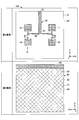
- FIG. 1 is a plan view of the planar antenna according to the first embodiment.
- a planar antenna 101 shown in FIG. 1 includes a dielectric layer 40 through which visible light passes, an antenna conductor 10 provided on one surface of the dielectric layer 40, and a ground conductor 20 opposed to the antenna conductor 10 via the dielectric layer 40. And a power supply line 30 for supplying power to the antenna conductor 10.
- the planar antenna 101 is called a patch antenna or a microstrip antenna.
- FIG. 2 is a plan view of the antenna conductor and the ground conductor of the planar antenna according to the first embodiment.
- the dielectric layer 40 has a first main surface 41 and a second main surface 42 opposite to the first main surface 41. 2 shows the antenna conductor 10 and the feed line 30 provided on the first main surface 41 of the dielectric layer 40. 2 shows the ground conductor 20 provided on the second main surface 42 of the dielectric layer 40.
- the first main surface 41 is an example of a first surface of the dielectric layer.
- the second main surface 42 is an example of a second surface of the dielectric layer opposite to the first surface.
- the dielectric layer 40 is a plate-like or sheet-like base material containing a dielectric as a main component. Both the first main surface 41 and the second main surface 42 are parallel to the XY plane.
- the dielectric layer 40 may be, for example, a dielectric substrate or a dielectric sheet. Examples of the material of the dielectric layer 40 include glass such as quartz glass, ceramics, fluorine-based resin such as polytetrafluoroethylene, liquid crystal polymer, and cycloolefin polymer, but the material is not limited thereto.
- the material of the dielectric layer 40 may be a transparent dielectric member that transmits visible light, and the transparent includes translucent.
- the visible light transmittance of the dielectric layer 40 is preferably, for example, 90% or more from the viewpoint of suppressing the blocking of the visual field.
- the antenna conductor 10 is a planar conductor pattern whose surface is parallel to the XY plane.
- the antenna conductor 10 is a conductor pattern formed on the first main surface 41, and may be formed by a conductor sheet or a conductor substrate disposed on the first main surface 41. Examples of the material of the conductor used for the antenna conductor 10 include, but are not limited to, silver and copper.
- the antenna conductor 10 has, for example, at least one patch conductor.
- the antenna conductor 10 forms an array antenna having four patch conductors 11, 12, 13, and 14.
- the antenna conductor 10 is a solid pattern including a region where the degree of transmission of visible light is lower than that of the dielectric layer 40.
- the entire antenna conductor 10 is formed of an opaque planar conductor including a plurality of patch conductors 11 to 14.
- the power supply line 30 is a planar conductor pattern whose surface is parallel to the XY plane.
- the power supply line 30 is a conductor pattern formed on the first main surface 41, and may be formed by a conductor sheet or a conductor substrate disposed on the first main surface 41. Examples of the material of the conductor used for the power supply line 30 include, but are not limited to, silver and copper.
- the feed line 30 is formed integrally with the antenna conductor 10.
- the power supply line 30 has one end 32 connected to a branch point 36 where a branch path to the patch conductors 11 and 12 and a branch path to the patch conductors 13 and 14 are connected, and an unillustrated external part such as an amplifier. And the other end 33 which is a power supply end connected to the device.
- the feed line 30 is a strip conductor extending in the Y-axis direction, and the end 32 is connected to the antenna conductor 10.
- the power supply line 30 is a solid pattern including a region where the degree of transmission of visible light is lower than that of the dielectric layer 40.
- the entire power supply line 30 is formed of an opaque planar conductor.
- the ground conductor 20 is a conductor pattern whose surface is parallel to the XY plane.
- the ground conductor 20 is a conductor pattern formed on the second main surface 42, and may be formed by a conductor sheet or a conductor substrate disposed on the second main surface 42. Examples of the material of the conductor used for the ground conductor 20 include silver and copper, but are not limited thereto.
- the ground conductor 20 has a linear ground conductor 27 formed so as to have a gap, and a planar ground conductor 26 connected to the linear ground conductor 27.
- the planar ground conductor 26 is a ground portion provided in a band shape on one end side of the second main surface 42.
- the planar ground conductor 26 is a ground electrode corresponding to the end 33 which is a power supply end.
- the linear grounding conductor 27 is formed in a mesh shape so as to form a gap, and the visual field (transparency) can be secured by the gap.
- a lattice-shaped gap is formed.
- the ground conductor 20 includes an outer edge linear conductor 28 that is in contact with the linear ground conductor 27 and forms an outer edge of the ground conductor 20.
- the outer edge linear conductor 28 surrounds the linear ground conductor 27.
- the outer edge linear conductor 28 may be arranged so as to surround a part of the linear ground conductor 27, but the outer edge linear conductor 28 itself need not be arranged. Regarding the presence or absence of the outer edge linear conductor 28, the same applies to the following embodiments.
- the ground conductor 20 is provided in the first region 21 overlapping the antenna conductor 10 and the second region 22 not overlapping the antenna conductor 10 in plan view. More specifically, in the first embodiment, the linear ground conductor 27 is formed in both the first region 21 and the second region 22.
- the second region 22 has a ratio of an area occupied by the ground conductor 20 to an area of ⁇ / 4 ⁇ ⁇ / 4, where ⁇ is an effective wavelength of a radio wave transmitted / received by the planar antenna 101 in the dielectric layer 40 (hereinafter, referred to as ⁇ / 4 ⁇ ⁇ / 4). (Also referred to as a ratio R) of 50% or less.
- ⁇ is an effective wavelength of a radio wave transmitted / received by the planar antenna 101 in the dielectric layer 40
- ⁇ / 4 ⁇ ⁇ / 4 an effective wavelength of a radio wave transmitted / received by the planar antenna 101 in the dielectric layer 40
- the plane antenna 101 when the planar antenna 101 is installed on the surface or inside of the window glass 200, the plane antenna 101 (in particular, the ground conductor 20) has a field of view through the window glass 200 by having the region 23 with the ratio R of 50% or less. Blocking can be suppressed.
- the ratio R is preferably 40% or less, and more preferably 30% or less.
- the lower limit of the ratio R is not particularly limited as long as it is more than 0%, but for ensuring a stable antenna gain, for example, the ratio R may be 2% or more, and is preferably 5% or more.
- the ratio R includes the region 23 of 50% or less and the ratio of the area occupied by the ground conductor 20 to the entire area of the second region 22 (hereinafter, also referred to as ratio R ′) is 50% or less, preferable.
- the ratio R ′ is preferably 40% or less, more preferably 30% or less.
- the lower limit of the ratio R ' is not particularly limited as long as it exceeds 0%.
- the ratio R' may be 2% or more, and is preferably 5% or more.
- the ratio R exceeds 50%, it is difficult to secure a visual field.
- the ratio R is less than 2%, for example, it is easy to secure the visual field, but it is difficult to secure the antenna gain.
- the ratio R ′ exceeds 50%, it is difficult to secure the visual field.
- the ratio R ′ is less than 2%, for example, it is easy to secure the visual field, but it may be difficult to secure the antenna gain.
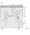
- FIG. 3 is a plan view of the planar antenna according to the second embodiment.
- the planar antenna 102 shown in FIG. 3 includes a dielectric layer 40 through which visible light passes, an antenna conductor 10 provided on one side of the dielectric layer 40, and a ground conductor 20 facing the antenna conductor 10 via the dielectric layer 40. And a power supply line 30 for supplying power to the antenna conductor 10.
- FIG. 4 is a plan view of the antenna conductor and the ground conductor of the planar antenna according to the second embodiment.
- each of the antenna conductor 10 and the feed line 30 includes a pattern having a region where the degree of transmission of visible light is lower than that of the dielectric layer 40.
- the antenna conductor 10 includes an internal linear conductor 17 formed such that a gap is formed inside the antenna conductor 10.
- the internal linear conductors 17 are formed in a mesh shape so as to form a lattice-shaped gap. At least a portion of the internal linear conductor 17 overlaps with the linear ground conductor 27 of the ground conductor 20 in a plan view, but all of the internal linear conductors 17 overlap with the linear ground conductor 27. More preferred. As described above, since both the antenna conductor 10 and the ground conductor 20 are formed by the linear conductors so as to form a gap, the visual field can be more easily secured.
- the antenna conductor 10 includes the outer linear conductor 18 that is in contact with the inner linear conductor 17 and forms the outer edge of the antenna conductor 10.
- the outer linear conductor 18 is in a closed state surrounding the inner linear conductor 17.
- the outer conductor 18 surrounds the inner conductor 17 in the antenna conductor 10, so that the difference from the current distribution in the case of the planar conductor as in the first embodiment can be suppressed. And good antenna characteristics.
- the power supply line 30 includes an internal linear conductor 37 formed so that a gap is formed inside the power supply line 30.
- the internal linear conductor 37 is formed in a mesh shape so as to form a lattice-shaped gap. At least a portion of the internal linear conductor 37 overlaps with the linear ground conductor 27 of the ground conductor 20 in a plan view, but all of the internal linear conductors 37 overlap with the linear ground conductor 27. More preferred. As described above, since both the power supply line 30 and the ground conductor 20 are formed by the linear conductors so as to form a gap, the visual field can be more easily secured.
- the power supply line 30 includes an outer edge linear conductor 38 that is in contact with the inner linear conductor 37 and forms an outer edge of the power supply line 30.
- the outer linear conductor 38 is in a closed state surrounding the inner linear conductor 37.
- the ground conductor 20 is provided in the first area 21 overlapping the antenna conductor 10 and the second area 22 not overlapping the antenna conductor 10 in plan view.
- the linear ground conductor 27 is formed in both the first region 21 and the second region 22.
- the ratio R of the area occupied by the ground conductor 20 per ⁇ / 4 ⁇ ⁇ / 4 area is 50, where ⁇ is the effective wavelength of the radio wave transmitted and received by the planar antenna 102 in the dielectric layer 40. % Region 23 or less. Therefore, when the second region 22 has such a region 23, the obstruction of the visual field is suppressed, and the planar antenna 102 having excellent directivity and desired transmission / reception sensitivity can be provided.
- the ratio R and the ratio R ' may be values within a preferable range similar to that of the first embodiment. Furthermore, in the case of the second embodiment, it is more preferable that the ratio of the area occupied by the antenna conductor 10 to the entire area of the first region 21 (hereinafter, also referred to as a ratio R ") is 50% or less. Also, like the ratio R, it is preferably 40% or less, and more preferably 30% or less. The lower limit of the ratio R "is not particularly limited as long as it exceeds 0%. However, in order to secure a stable antenna gain, for example, the ratio R" may be 2% or more, and is preferably 5% or more.
- FIG. 5A to 5D are plan views showing other forms of the power supply line 30 in the second embodiment.
- FIG. 5A is a plan view of the power supply line 60a.
- the power supply line 60a has a first power supply line 61 and a second power supply line 62.
- the second power supply line 62 is located between the antenna conductor 10 and the first power supply line 61, and one end is connected to the antenna conductor 10 and the other end is connected to the first power supply line 61.
- the first power supply line 61 has a higher density of conductors per unit area (for example, 1 mm 2 ) than the second power supply line 62 and includes, for example, a part of a solid region having a transmittance of 0% with respect to visible light.
- a configuration may be used, or a configuration in which all of the regions are solid.
- the second power supply line 62 has higher transparency than the first power supply line 61.
- the conductor density of a portion that does not require transparency may be increased to increase the transmission efficiency.
- a conductor density of the portion is higher than other portions.
- the power supply line 60a illustrated in FIG. 5A has a first power supply line 61 and a second power supply line 62 that are adjacent to each other, and includes a boundary line 63 that is a boundary therebetween.
- the first power supply line 61 is a combination in which the entire area is formed of a conductor and the second power supply line 62 has a mesh shape as described above
- the second power supply line 62 has Impedance mismatch occurs and transmission loss easily occurs.
- FIGS. 5A to 5D are plan views showing the feed lines 60a to 60d showing various forms in which impedance mismatch due to the boundary line 63 is suppressed and impedance matching is possible.
- the power supply line 60a shown in FIG. 5A has a configuration in which the width of the first power supply line 61 is constant and the width is smaller than the width of the second power supply line 62.
- the first power supply line 61 has two or more portions having different widths.
- the power supply line 60 b has a first portion 64 including the boundary line 63 and a second portion 65 (not including the boundary line 63), and the width of the first portion 64 is equal to the width of the second power supply line 62. It is smaller than the width and the width of the second portion 65.
- the first portion 64 may be provided so as to function as a transformer whose length in the Y-axis direction is 1 / of the wavelength.
- the design of the impedance transformer becomes easy.
- ⁇ of the wavelength may be, for example, 1 / times the effective wavelength ⁇ when the power supply line 30 is formed on the dielectric layer.
- the width and length (in the Y-axis direction) of the first portion 64 and the width of the second portion 65 can be set to be adjusted to a predetermined impedance.
- the power supply line 60d shown in FIG. 5D has a form in which the width of the first power supply line 61 and the width of the second power supply line 62 are the same, and has two or more portions where the conductor density of the first power supply line 61 is different. is there.
- a first portion 66, a second portion 67, and a third portion 68 are arranged in this order, and the first portion 66 is in contact with the boundary 63.
- the conductor density of the first portion 66 is the lowest, and the conductor density of the second portion 67 and the third portion 68 is lower. Higher configuration.
- the power supply line 30 in the second embodiment is not limited to the power supply lines 60a to 60d shown in FIGS. 5A to 5D, and can be appropriately adjusted to a conductor density so as to enable impedance matching.
- the shape can be appropriately adjusted to a combination of the forms.
- FIG. 6 is a plan view of the antenna conductor and the ground conductor of the planar antenna according to the third embodiment. 6 includes a dielectric layer 40 through which visible light passes, an antenna conductor 10 provided on one surface of the dielectric layer 40, and a ground conductor 20 facing the antenna conductor 10 via the dielectric layer 40. And a power supply line 30 for supplying power to the antenna conductor 10.
- planar antenna 103 of the third embodiment shown in FIG. 6 looks like the same shape shown in FIG. 1 in plan view.
- the form of the ground conductor 20 is different from that of the first embodiment shown in FIG.
- the ground conductor 20 includes a planar ground conductor 25 entirely overlapping the antenna conductor 10 in plan view. Since the planar antenna conductor 10 and the planar ground conductor 25 face each other, the level of the ground portion as the planar ground conductor 25 is stabilized. Furthermore, since the planar antenna conductor 10 and the planar ground conductor 25 are opposed to each other, the planar ground conductor 25 is located on the back side of the patch serving as a main radiation source (the planar antenna conductor 10). Therefore, since the planar ground conductor 25 functions as a reflector, the directivity and antenna gain on the front side (+ Z side) of the patch can be improved. In the third embodiment, the planar ground conductor 25 has the same shape as the antenna conductor 10 in plan view.
- the planar ground conductor 25 may partially overlap the antenna conductor 10 so that a part of the planar ground conductor 25 protrudes from the antenna conductor 10 in a plan view, The part may overlap the antenna conductor 10 so that the part is inside the outer edge of the antenna conductor 10.
- the grounding conductor 20 includes a planar grounding conductor 29 that entirely overlaps the power supply line 30 in plan view. Since the planar power supply line 30 and the planar ground conductor 29 face each other, the operation as the power supply line is stabilized. In the third embodiment, the planar ground conductor 29 has the same shape as the power supply line 30 in plan view. Thereby, it is easy to secure the visual field.
- the planar ground conductor 29 may overlap with the power supply line 30 so that a part of the planar ground conductor 29 protrudes from the power supply line 30 in a plan view.
- the power supply line 30 may partially overlap the power supply line 30 so that the power supply line 30 is partially inside the outer edge of the power supply line 30.
- FIG. 7 is a plan view of a plurality of linear conductors crossing each other.
- the line width W of the linear ground conductor 27 is preferably from 1 to 500 ⁇ m from the viewpoint of securing a visual field. If the line width W is less than 1 ⁇ m, the antenna gain may not be stable because the ground (earth) is not stabilized. If the line width W exceeds 500 ⁇ m, it is difficult to secure a visual field. Therefore, when the line width W is 1 to 500 ⁇ m, both stable antenna gain and a sufficient field of view can be ensured. Further, the line width W is preferably from 3 to 200 ⁇ m, more preferably from 5 to 50 ⁇ m.
- the linear ground conductor 27 includes a first linear ground conductor extending in the first linear direction 51 and a second linear ground conductor extending in a second linear direction 52 orthogonal to the first linear direction 51. .
- the ground is stabilized, and variations in antenna characteristics can be suppressed.
- FIG. 7 shows a state in which two first linear ground conductors and two second linear ground conductors intersect.
- the line width W of the linear ground conductor 27 is preferably 0.5 to 30% with respect to the pitch P1 (or the pitch P2) from the viewpoint of securing a visual field. If the line width W is less than 0.5% with respect to the pitch P1 or the pitch P2, the antenna gain may not be stable because the ground (earth) is not stabilized. If the line width W is more than 30% of the pitch P1 or the pitch P2, it is difficult to secure a visual field.
- the line width W is 0.5 to 30% with respect to the pitch P1 (or the pitch P2), it is possible to achieve both a stable antenna gain and a secure view. Further, the line width W is preferably 0.7% to 23% with respect to the pitch P1 (or the pitch P2), and more preferably 1% to 15%.
- the length L of the outer edge of the region 53 surrounded by the linear ground conductor 27 is preferably 1 ⁇ or less with respect to the effective wavelength ⁇ of the dielectric layer 40, from the viewpoint of improving the antenna gain. If the length L exceeds 1 ⁇ , unnecessary resonance occurs in the linear ground conductor, and it becomes difficult to secure antenna performance.
- FIG. 8 is a plan view of a planar antenna according to a comparative example. 8 includes a dielectric layer 40 through which visible light is transmitted, an antenna conductor 110 provided on one surface of the dielectric layer 40, and a ground conductor 120 facing the antenna conductor 110 via the dielectric layer 40. And a power supply line 130 for supplying power to the antenna conductor 110. 8, the form of the ground conductor is different from that of the first embodiment shown in FIGS.
- the ground conductor 120 shown in FIG. 8 is a solid pattern composed of a region where the degree of transmission of visible light is lower than that of the dielectric layer 40.
- the whole ground conductor 120 is formed of an opaque planar conductor.
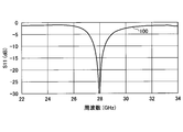
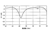
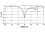
- FIG. 9 is a diagram illustrating an example of the return loss characteristic of the planar antenna 100 according to the comparative example.
- FIG. 10 is a diagram illustrating an example of the return loss characteristics of the planar antenna 101 according to the first embodiment.
- FIG. 11 is a diagram illustrating an example of a return loss characteristic of the planar antenna 103 according to the third embodiment. 9 to 11, S11 on the vertical axis indicates a return loss characteristic.
- the planar antennas 101 and 103 of this embodiment have sufficient return loss characteristics.
- the field of view is blocked because the ground conductor 120 is a planar conductor. Therefore, the planar antennas 101 and 103 of the present embodiment can obtain a sufficient return loss characteristic while suppressing the obstruction of the field of view.
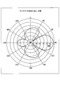
- FIGS. 12 to 14 are diagrams showing examples of directivity on the E plane of the planar antennas 100, 101, and 103, respectively.
- 15 to 17 are diagrams illustrating examples of directivity on the H plane of the planar antennas 100, 101, and 103, respectively.
- the E plane represents a YZ plane passing through the branch point 36
- the H plane represents a ZX plane passing through the branch point 36.
- the planar antennas 101 and 103 of the present embodiment can obtain the same antenna gain and the same directivity as the planar antenna 100. Therefore, the planar antennas 101 and 103 of the present embodiment have excellent directivity and have desired transmission / reception sensitivity while suppressing obstruction of the field of view.
- the planar antenna 101 of the first embodiment has high transmission / reception sensitivity to radio waves of 26.5 GHz.
- the ratio (R) of the area occupied by the ground conductor 20 per area of ⁇ ⁇ / 4 was set to 20%.
- the pitch P2 between the adjacent first linear ground conductors and the pitch P1 between the adjacent second linear ground conductors are equal to each other, that is, 847 ⁇ m.
- the line width W was 100 ⁇ m, and the ratio of the line width W to the pitches P1 and P2 was 12%.
- the planar antenna 103 according to the third embodiment has high transmission / reception sensitivity to radio waves of 28 GHz, and the second main surface 42 has ⁇ / 4 ⁇ ⁇
- the ratio (R) of the area occupied by the ground conductor 20 per ⁇ area was set to 20%.
- the pitch P2 between the adjacent first linear ground conductors and the pitch P1 between the adjacent second linear ground conductors are equal to each other, that is, 847 ⁇ m.
- the line width W was 100 ⁇ m, and the ratio of the line width W to the pitches P1 and P2 was 12%.
- the planar antenna 100 of the comparative example has high transmission / reception sensitivity to radio waves of 28 GHz in the examples shown in FIGS. 9, 12 and 15, and the second main surface 42 has ⁇ / 4 ⁇ ⁇ / 4.
- the ratio (R) of the area occupied by the ground conductor 20 per area is 100%.
- planar antennas 100, 101, and 103 of the examples shown in FIGS. 9 to 17 the common dimensions of the respective parts are as shown in FIG.
- planar antenna and the window glass have been described above with reference to the embodiments, the present invention is not limited to the above embodiments. Various modifications and improvements, such as combinations and substitutions with some or all of the other embodiments, are possible within the scope of the present invention.
- the antenna conductor may have a lower or higher visible light transmission degree than the dielectric layer, or may have the same transmittance as the dielectric layer. Further, the linear conductor may be formed in a mesh shape so as to form a gap, or may be formed in a stripe shape so as to form a gap.
- the outer shape of the antenna conductor may be another shape such as a circle. Further, the antenna conductor may be fed by another feeding line such as a feeding pin or a through hole.
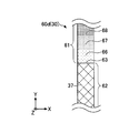
- FIG. 19 is a perspective view of the planar antenna according to the fourth embodiment in which the feed line 30 is configured by a coplanar line.
- the planar antenna 104 includes a dielectric layer 40 through which visible light passes, an antenna conductor 10 provided on one surface of the dielectric layer 40, a ground conductor 20 opposed to the antenna conductor 10 via the dielectric layer 40, 10 is provided with a power supply line 30 for supplying power via a slot 31.
- the feed line 30 and the ground conductor 20 are formed on the second main surface of the dielectric layer 40 (the surface opposite to the first main surface 41 on which the antenna conductor 10 is formed).
- the power supply line 30 has a pair of gaps running in parallel and a center conductor sandwiched between the pair of gaps.
- the slot 31 formed at one end of the feed line 30 and the antenna conductor 10 formed on the first main surface 41 are coupled at a high frequency.
- the ground conductor 20 has a linear ground conductor 27 formed so as to form a gap, and the linear ground conductor 27 is formed in a mesh shape so as to form a gap.
- the view (transparency) can be secured.
- at least one of the center conductor of the power supply line 30 and the antenna conductor 10 may have a linear conductor formed so as to form a gap. Thereby, further transparency can be secured.
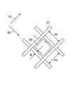
- FIG. 20 is a perspective view of the planar antenna according to the fifth embodiment. Description of the same configuration and effect as the fifth embodiment will be omitted by using the description of the above embodiment.
- the planar antenna 105 includes dielectric layers 40A and 40B through which visible light passes, an antenna conductor 10 provided on one surface of the dielectric layer 40A, and a ground conductor 20 facing the antenna conductor 10 via the dielectric layer 40A. A feed line 30 for feeding power to the antenna conductor 10 via the slot 31;
- the ground conductor 20 is sandwiched between a pair of dielectric layers 40A and 40B.
- the antenna conductor 10 is a patch conductor formed on the surface of the first dielectric layer 40A.
- the power supply line 30 is a microstrip line formed on the surface of the second dielectric layer 40B.
- the antenna conductor 10 is fed and excited by electromagnetic coupling between the antenna conductor 10 and the feed line 30 via the slot 31 provided in the ground conductor 20.
- the ground conductor 20 shown in FIG. 20 has a linear ground conductor formed so as to form a gap.
- a visual field (transparency) can be secured by the gap.
- at least one of the power supply line 30 and the antenna conductor 10 may have a linear conductor formed so as to form a gap. Thereby, further transparency can be secured.
Abstract
L'invention concerne une antenne planaire comprenant une couche diélectrique qui transmet la lumière visible et qui a une première surface et une seconde surface opposée à la première surface, un conducteur d'antenne qui est disposé sur la première surface, et un conducteur de masse qui est disposé sur la seconde surface. Dans une vue en plan, le conducteur de masse est agencé dans une première région qui chevauche le conducteur d'antenne et une seconde région qui ne chevauche pas le conducteur d'antenne. Définissant λ comme longueur d'onde effective dans la couche diélectrique des ondes radio émises et reçues par l'antenne planaire, la seconde région a une région dans laquelle le rapport de la surface occupée par le conducteur de masse par λ /4 × λ /4 est inférieur ou égal à 50 %.
Priority Applications (1)
| Application Number | Priority Date | Filing Date | Title |
|---|---|---|---|
| JP2020550421A JP7355026B2 (ja) | 2018-10-03 | 2019-09-30 | 平面アンテナ及び窓ガラス |
Applications Claiming Priority (2)
| Application Number | Priority Date | Filing Date | Title |
|---|---|---|---|
| JP2018-188584 | 2018-10-03 | ||
| JP2018188584 | 2018-10-03 |
Publications (1)
| Publication Number | Publication Date |
|---|---|
| WO2020071316A1 true WO2020071316A1 (fr) | 2020-04-09 |
Family
ID=70054654
Family Applications (1)
| Application Number | Title | Priority Date | Filing Date |
|---|---|---|---|
| PCT/JP2019/038526 WO2020071316A1 (fr) | 2018-10-03 | 2019-09-30 | Antenne planaire et vitre de fenêtre |
Country Status (2)
| Country | Link |
|---|---|
| JP (1) | JP7355026B2 (fr) |
| WO (1) | WO2020071316A1 (fr) |
Cited By (3)
| Publication number | Priority date | Publication date | Assignee | Title |
|---|---|---|---|---|
| CN111509372A (zh) * | 2020-05-09 | 2020-08-07 | 成都理工大学 | 一种汽车防撞雷达阵列天线 |
| WO2023171727A1 (fr) * | 2022-03-10 | 2023-09-14 | Tdk株式会社 | Trajet de transmission, antenne et dispositif d'affichage |
| WO2023171545A1 (fr) * | 2022-03-08 | 2023-09-14 | Agc株式会社 | Unité d'antenne et vitre |
Citations (4)
| Publication number | Priority date | Publication date | Assignee | Title |
|---|---|---|---|---|
| JPH024306U (fr) * | 1988-06-22 | 1990-01-11 | ||
| JPH11177336A (ja) * | 1997-10-17 | 1999-07-02 | Sharp Corp | 透明アンテナ及び無線通信装置 |
| JP2006303846A (ja) * | 2005-04-20 | 2006-11-02 | Japan Radio Co Ltd | グリッドパッチアンテナ |
| US20120287018A1 (en) * | 2011-05-11 | 2012-11-15 | Harris Corporation, Corporation Of The State Of Delaware | Electronic device including a patch antenna and photovoltaic layer and related methods |
Family Cites Families (2)
| Publication number | Priority date | Publication date | Assignee | Title |
|---|---|---|---|---|
| GB9808042D0 (en) * | 1998-04-15 | 1998-06-17 | Harada Ind Europ Limited | Patch antenna |
| CN101180765B (zh) * | 2005-04-01 | 2013-06-05 | 日本写真印刷株式会社 | 显示器用透明天线和带天线的显示器用透光性构件以及带天线的壳体用构件 |
-
2019
- 2019-09-30 WO PCT/JP2019/038526 patent/WO2020071316A1/fr active Application Filing
- 2019-09-30 JP JP2020550421A patent/JP7355026B2/ja active Active
Patent Citations (4)
| Publication number | Priority date | Publication date | Assignee | Title |
|---|---|---|---|---|
| JPH024306U (fr) * | 1988-06-22 | 1990-01-11 | ||
| JPH11177336A (ja) * | 1997-10-17 | 1999-07-02 | Sharp Corp | 透明アンテナ及び無線通信装置 |
| JP2006303846A (ja) * | 2005-04-20 | 2006-11-02 | Japan Radio Co Ltd | グリッドパッチアンテナ |
| US20120287018A1 (en) * | 2011-05-11 | 2012-11-15 | Harris Corporation, Corporation Of The State Of Delaware | Electronic device including a patch antenna and photovoltaic layer and related methods |
Cited By (3)
| Publication number | Priority date | Publication date | Assignee | Title |
|---|---|---|---|---|
| CN111509372A (zh) * | 2020-05-09 | 2020-08-07 | 成都理工大学 | 一种汽车防撞雷达阵列天线 |
| WO2023171545A1 (fr) * | 2022-03-08 | 2023-09-14 | Agc株式会社 | Unité d'antenne et vitre |
| WO2023171727A1 (fr) * | 2022-03-10 | 2023-09-14 | Tdk株式会社 | Trajet de transmission, antenne et dispositif d'affichage |
Also Published As
| Publication number | Publication date |
|---|---|
| JPWO2020071316A1 (ja) | 2021-09-02 |
| JP7355026B2 (ja) | 2023-10-03 |
Similar Documents
| Publication | Publication Date | Title |
|---|---|---|
| CN112771719B (zh) | 天线系统 | |
| WO2020071316A1 (fr) | Antenne planaire et vitre de fenêtre | |
| US9472855B2 (en) | Antenna device | |
| US8378894B2 (en) | Antenna device | |
| KR20050046630A (ko) | 안테나 장치 | |
| US11276940B2 (en) | Waveguide slot array antenna | |
| US10840592B2 (en) | Electronic device and antenna assembly thereof | |
| US8736514B2 (en) | Antenna | |
| US20210143535A1 (en) | Array antenna apparatus and communication device | |
| WO2015025566A1 (fr) | Antenne | |
| US11967768B2 (en) | Slot array antenna | |
| US20230318192A1 (en) | Antenna | |
| KR20110110703A (ko) | 전자기파 필터 장치 | |
| CN110247174A (zh) | 宽带非对称缝隙天线 | |
| US20230094901A1 (en) | Planar antenna and high-frequency module including same | |
| EP3972050A1 (fr) | Ensemble antenne et dispositif électronique | |
| KR20210087933A (ko) | 동축 커넥터 및 동축 커넥터를 갖는 기판 | |
| WO2023223893A1 (fr) | Dispositif d'antenne | |
| KR20080006415A (ko) | 광자밴드갭 구조의 안테나 | |
| JP7211416B2 (ja) | スロットアレイアンテナ | |
| TWI752780B (zh) | 寬波束之天線結構 | |
| KR102319004B1 (ko) | 차량용 광대역 평면 역원추 안테나 | |
| WO2022202623A1 (fr) | Dispositif d'antenne et dispositif de communication | |
| WO2023032046A1 (fr) | Antenne dipôle et antenne réseau | |
| CN114784511A (zh) | 一种天线装置及终端设备 |
Legal Events
| Date | Code | Title | Description |
|---|---|---|---|
| 121 | Ep: the epo has been informed by wipo that ep was designated in this application |
Ref document number: 19868324 Country of ref document: EP Kind code of ref document: A1 |
|
| ENP | Entry into the national phase |
Ref document number: 2020550421 Country of ref document: JP Kind code of ref document: A |
|
| NENP | Non-entry into the national phase |
Ref country code: DE |
|
| 122 | Ep: pct application non-entry in european phase |
Ref document number: 19868324 Country of ref document: EP Kind code of ref document: A1 |