WO2020071110A1 - 調光素子の製造方法 - Google Patents
調光素子の製造方法Info
- Publication number
- WO2020071110A1 WO2020071110A1 PCT/JP2019/036446 JP2019036446W WO2020071110A1 WO 2020071110 A1 WO2020071110 A1 WO 2020071110A1 JP 2019036446 W JP2019036446 W JP 2019036446W WO 2020071110 A1 WO2020071110 A1 WO 2020071110A1
- Authority
- WO
- WIPO (PCT)
- Prior art keywords
- transparent electrode
- light control
- liquid crystal
- layer
- electrode layer
- Prior art date
- Legal status (The legal status is an assumption and is not a legal conclusion. Google has not performed a legal analysis and makes no representation as to the accuracy of the status listed.)
- Ceased
Links
Images
Classifications
-
- B—PERFORMING OPERATIONS; TRANSPORTING
- B32—LAYERED PRODUCTS
- B32B—LAYERED PRODUCTS, i.e. PRODUCTS BUILT-UP OF STRATA OF FLAT OR NON-FLAT, e.g. CELLULAR OR HONEYCOMB, FORM
- B32B43/00—Operations specially adapted for layered products and not otherwise provided for, e.g. repairing; Apparatus therefor
- B32B43/006—Delaminating
-
- G—PHYSICS
- G02—OPTICS
- G02F—OPTICAL DEVICES OR ARRANGEMENTS FOR THE CONTROL OF LIGHT BY MODIFICATION OF THE OPTICAL PROPERTIES OF THE MEDIA OF THE ELEMENTS INVOLVED THEREIN; NON-LINEAR OPTICS; FREQUENCY-CHANGING OF LIGHT; OPTICAL LOGIC ELEMENTS; OPTICAL ANALOGUE/DIGITAL CONVERTERS
- G02F1/00—Devices or arrangements for the control of the intensity, colour, phase, polarisation or direction of light arriving from an independent light source, e.g. switching, gating or modulating; Non-linear optics
- G02F1/01—Devices or arrangements for the control of the intensity, colour, phase, polarisation or direction of light arriving from an independent light source, e.g. switching, gating or modulating; Non-linear optics for the control of the intensity, phase, polarisation or colour
- G02F1/13—Devices or arrangements for the control of the intensity, colour, phase, polarisation or direction of light arriving from an independent light source, e.g. switching, gating or modulating; Non-linear optics for the control of the intensity, phase, polarisation or colour based on liquid crystals, e.g. single liquid crystal display cells
- G02F1/133—Constructional arrangements; Operation of liquid crystal cells; Circuit arrangements
- G02F1/1333—Constructional arrangements; Manufacturing methods
- G02F1/1334—Constructional arrangements; Manufacturing methods based on polymer dispersed liquid crystals, e.g. microencapsulated liquid crystals
-
- G—PHYSICS
- G02—OPTICS
- G02F—OPTICAL DEVICES OR ARRANGEMENTS FOR THE CONTROL OF LIGHT BY MODIFICATION OF THE OPTICAL PROPERTIES OF THE MEDIA OF THE ELEMENTS INVOLVED THEREIN; NON-LINEAR OPTICS; FREQUENCY-CHANGING OF LIGHT; OPTICAL LOGIC ELEMENTS; OPTICAL ANALOGUE/DIGITAL CONVERTERS
- G02F1/00—Devices or arrangements for the control of the intensity, colour, phase, polarisation or direction of light arriving from an independent light source, e.g. switching, gating or modulating; Non-linear optics
- G02F1/01—Devices or arrangements for the control of the intensity, colour, phase, polarisation or direction of light arriving from an independent light source, e.g. switching, gating or modulating; Non-linear optics for the control of the intensity, phase, polarisation or colour
- G02F1/13—Devices or arrangements for the control of the intensity, colour, phase, polarisation or direction of light arriving from an independent light source, e.g. switching, gating or modulating; Non-linear optics for the control of the intensity, phase, polarisation or colour based on liquid crystals, e.g. single liquid crystal display cells
- G02F1/1316—Methods for cleaning the liquid crystal cells, or components thereof, during manufacture: Materials therefor
-
- G—PHYSICS
- G02—OPTICS
- G02F—OPTICAL DEVICES OR ARRANGEMENTS FOR THE CONTROL OF LIGHT BY MODIFICATION OF THE OPTICAL PROPERTIES OF THE MEDIA OF THE ELEMENTS INVOLVED THEREIN; NON-LINEAR OPTICS; FREQUENCY-CHANGING OF LIGHT; OPTICAL LOGIC ELEMENTS; OPTICAL ANALOGUE/DIGITAL CONVERTERS
- G02F1/00—Devices or arrangements for the control of the intensity, colour, phase, polarisation or direction of light arriving from an independent light source, e.g. switching, gating or modulating; Non-linear optics
- G02F1/01—Devices or arrangements for the control of the intensity, colour, phase, polarisation or direction of light arriving from an independent light source, e.g. switching, gating or modulating; Non-linear optics for the control of the intensity, phase, polarisation or colour
- G02F1/13—Devices or arrangements for the control of the intensity, colour, phase, polarisation or direction of light arriving from an independent light source, e.g. switching, gating or modulating; Non-linear optics for the control of the intensity, phase, polarisation or colour based on liquid crystals, e.g. single liquid crystal display cells
- G02F1/133—Constructional arrangements; Operation of liquid crystal cells; Circuit arrangements
- G02F1/1333—Constructional arrangements; Manufacturing methods
- G02F1/1343—Electrodes
-
- G—PHYSICS
- G02—OPTICS
- G02F—OPTICAL DEVICES OR ARRANGEMENTS FOR THE CONTROL OF LIGHT BY MODIFICATION OF THE OPTICAL PROPERTIES OF THE MEDIA OF THE ELEMENTS INVOLVED THEREIN; NON-LINEAR OPTICS; FREQUENCY-CHANGING OF LIGHT; OPTICAL LOGIC ELEMENTS; OPTICAL ANALOGUE/DIGITAL CONVERTERS
- G02F1/00—Devices or arrangements for the control of the intensity, colour, phase, polarisation or direction of light arriving from an independent light source, e.g. switching, gating or modulating; Non-linear optics
- G02F1/01—Devices or arrangements for the control of the intensity, colour, phase, polarisation or direction of light arriving from an independent light source, e.g. switching, gating or modulating; Non-linear optics for the control of the intensity, phase, polarisation or colour
- G02F1/13—Devices or arrangements for the control of the intensity, colour, phase, polarisation or direction of light arriving from an independent light source, e.g. switching, gating or modulating; Non-linear optics for the control of the intensity, phase, polarisation or colour based on liquid crystals, e.g. single liquid crystal display cells
- G02F1/133—Constructional arrangements; Operation of liquid crystal cells; Circuit arrangements
- G02F1/1333—Constructional arrangements; Manufacturing methods
- G02F1/1343—Electrodes
- G02F1/13439—Electrodes characterised by their electrical, optical, physical properties; materials therefor; method of making
-
- G—PHYSICS
- G02—OPTICS
- G02F—OPTICAL DEVICES OR ARRANGEMENTS FOR THE CONTROL OF LIGHT BY MODIFICATION OF THE OPTICAL PROPERTIES OF THE MEDIA OF THE ELEMENTS INVOLVED THEREIN; NON-LINEAR OPTICS; FREQUENCY-CHANGING OF LIGHT; OPTICAL LOGIC ELEMENTS; OPTICAL ANALOGUE/DIGITAL CONVERTERS
- G02F1/00—Devices or arrangements for the control of the intensity, colour, phase, polarisation or direction of light arriving from an independent light source, e.g. switching, gating or modulating; Non-linear optics
- G02F1/01—Devices or arrangements for the control of the intensity, colour, phase, polarisation or direction of light arriving from an independent light source, e.g. switching, gating or modulating; Non-linear optics for the control of the intensity, phase, polarisation or colour
- G02F1/13—Devices or arrangements for the control of the intensity, colour, phase, polarisation or direction of light arriving from an independent light source, e.g. switching, gating or modulating; Non-linear optics for the control of the intensity, phase, polarisation or colour based on liquid crystals, e.g. single liquid crystal display cells
- G02F1/133—Constructional arrangements; Operation of liquid crystal cells; Circuit arrangements
- G02F1/1333—Constructional arrangements; Manufacturing methods
- G02F1/1345—Conductors connecting electrodes to cell terminals
-
- G—PHYSICS
- G02—OPTICS
- G02F—OPTICAL DEVICES OR ARRANGEMENTS FOR THE CONTROL OF LIGHT BY MODIFICATION OF THE OPTICAL PROPERTIES OF THE MEDIA OF THE ELEMENTS INVOLVED THEREIN; NON-LINEAR OPTICS; FREQUENCY-CHANGING OF LIGHT; OPTICAL LOGIC ELEMENTS; OPTICAL ANALOGUE/DIGITAL CONVERTERS
- G02F1/00—Devices or arrangements for the control of the intensity, colour, phase, polarisation or direction of light arriving from an independent light source, e.g. switching, gating or modulating; Non-linear optics
- G02F1/01—Devices or arrangements for the control of the intensity, colour, phase, polarisation or direction of light arriving from an independent light source, e.g. switching, gating or modulating; Non-linear optics for the control of the intensity, phase, polarisation or colour
- G02F1/13—Devices or arrangements for the control of the intensity, colour, phase, polarisation or direction of light arriving from an independent light source, e.g. switching, gating or modulating; Non-linear optics for the control of the intensity, phase, polarisation or colour based on liquid crystals, e.g. single liquid crystal display cells
- G02F1/133—Constructional arrangements; Operation of liquid crystal cells; Circuit arrangements
- G02F1/1333—Constructional arrangements; Manufacturing methods
- G02F1/1345—Conductors connecting electrodes to cell terminals
- G02F1/13458—Terminal pads
-
- B—PERFORMING OPERATIONS; TRANSPORTING
- B32—LAYERED PRODUCTS
- B32B—LAYERED PRODUCTS, i.e. PRODUCTS BUILT-UP OF STRATA OF FLAT OR NON-FLAT, e.g. CELLULAR OR HONEYCOMB, FORM
- B32B38/00—Ancillary operations in connection with laminating processes
- B32B38/10—Removing layers, or parts of layers, mechanically or chemically
-
- Y—GENERAL TAGGING OF NEW TECHNOLOGICAL DEVELOPMENTS; GENERAL TAGGING OF CROSS-SECTIONAL TECHNOLOGIES SPANNING OVER SEVERAL SECTIONS OF THE IPC; TECHNICAL SUBJECTS COVERED BY FORMER USPC CROSS-REFERENCE ART COLLECTIONS [XRACs] AND DIGESTS
- Y10—TECHNICAL SUBJECTS COVERED BY FORMER USPC
- Y10S—TECHNICAL SUBJECTS COVERED BY FORMER USPC CROSS-REFERENCE ART COLLECTIONS [XRACs] AND DIGESTS
- Y10S156/00—Adhesive bonding and miscellaneous chemical manufacture
- Y10S156/918—Delaminating processes adapted for specified product, e.g. delaminating medical specimen slide
- Y10S156/919—Delaminating in preparation for post processing recycling step
- Y10S156/922—Specified electronic component delaminating in preparation for recycling
- Y10S156/924—Delaminating display screen, e.g. cathode-ray, LCD screen
-
- Y—GENERAL TAGGING OF NEW TECHNOLOGICAL DEVELOPMENTS; GENERAL TAGGING OF CROSS-SECTIONAL TECHNOLOGIES SPANNING OVER SEVERAL SECTIONS OF THE IPC; TECHNICAL SUBJECTS COVERED BY FORMER USPC CROSS-REFERENCE ART COLLECTIONS [XRACs] AND DIGESTS
- Y10—TECHNICAL SUBJECTS COVERED BY FORMER USPC
- Y10S—TECHNICAL SUBJECTS COVERED BY FORMER USPC CROSS-REFERENCE ART COLLECTIONS [XRACs] AND DIGESTS
- Y10S156/00—Adhesive bonding and miscellaneous chemical manufacture
- Y10S156/934—Apparatus having delaminating means adapted for delaminating a specified article
- Y10S156/935—Delaminating means in preparation for post consumer recycling
- Y10S156/937—Means for delaminating specified electronic component in preparation for recycling
-
- Y—GENERAL TAGGING OF NEW TECHNOLOGICAL DEVELOPMENTS; GENERAL TAGGING OF CROSS-SECTIONAL TECHNOLOGIES SPANNING OVER SEVERAL SECTIONS OF THE IPC; TECHNICAL SUBJECTS COVERED BY FORMER USPC CROSS-REFERENCE ART COLLECTIONS [XRACs] AND DIGESTS
- Y10—TECHNICAL SUBJECTS COVERED BY FORMER USPC
- Y10T—TECHNICAL SUBJECTS COVERED BY FORMER US CLASSIFICATION
- Y10T156/00—Adhesive bonding and miscellaneous chemical manufacture
- Y10T156/11—Methods of delaminating, per se; i.e., separating at bonding face
- Y10T156/1111—Using solvent during delaminating [e.g., water dissolving adhesive at bonding face during delamination, etc.]
-
- Y—GENERAL TAGGING OF NEW TECHNOLOGICAL DEVELOPMENTS; GENERAL TAGGING OF CROSS-SECTIONAL TECHNOLOGIES SPANNING OVER SEVERAL SECTIONS OF THE IPC; TECHNICAL SUBJECTS COVERED BY FORMER USPC CROSS-REFERENCE ART COLLECTIONS [XRACs] AND DIGESTS
- Y10—TECHNICAL SUBJECTS COVERED BY FORMER USPC
- Y10T—TECHNICAL SUBJECTS COVERED BY FORMER US CLASSIFICATION
- Y10T156/00—Adhesive bonding and miscellaneous chemical manufacture
- Y10T156/11—Methods of delaminating, per se; i.e., separating at bonding face
- Y10T156/1111—Using solvent during delaminating [e.g., water dissolving adhesive at bonding face during delamination, etc.]
- Y10T156/1116—Using specified organic delamination solvent
-
- Y—GENERAL TAGGING OF NEW TECHNOLOGICAL DEVELOPMENTS; GENERAL TAGGING OF CROSS-SECTIONAL TECHNOLOGIES SPANNING OVER SEVERAL SECTIONS OF THE IPC; TECHNICAL SUBJECTS COVERED BY FORMER USPC CROSS-REFERENCE ART COLLECTIONS [XRACs] AND DIGESTS
- Y10—TECHNICAL SUBJECTS COVERED BY FORMER USPC
- Y10T—TECHNICAL SUBJECTS COVERED BY FORMER US CLASSIFICATION
- Y10T156/00—Adhesive bonding and miscellaneous chemical manufacture
- Y10T156/11—Methods of delaminating, per se; i.e., separating at bonding face
- Y10T156/1142—Changing dimension during delaminating [e.g., crushing, expanding, warping, etc.]
- Y10T156/1147—Using shrinking or swelling agent during delaminating
-
- Y—GENERAL TAGGING OF NEW TECHNOLOGICAL DEVELOPMENTS; GENERAL TAGGING OF CROSS-SECTIONAL TECHNOLOGIES SPANNING OVER SEVERAL SECTIONS OF THE IPC; TECHNICAL SUBJECTS COVERED BY FORMER USPC CROSS-REFERENCE ART COLLECTIONS [XRACs] AND DIGESTS
- Y10—TECHNICAL SUBJECTS COVERED BY FORMER USPC
- Y10T—TECHNICAL SUBJECTS COVERED BY FORMER US CLASSIFICATION
- Y10T156/00—Adhesive bonding and miscellaneous chemical manufacture
- Y10T156/11—Methods of delaminating, per se; i.e., separating at bonding face
- Y10T156/1168—Gripping and pulling work apart during delaminating
-
- Y—GENERAL TAGGING OF NEW TECHNOLOGICAL DEVELOPMENTS; GENERAL TAGGING OF CROSS-SECTIONAL TECHNOLOGIES SPANNING OVER SEVERAL SECTIONS OF THE IPC; TECHNICAL SUBJECTS COVERED BY FORMER USPC CROSS-REFERENCE ART COLLECTIONS [XRACs] AND DIGESTS
- Y10—TECHNICAL SUBJECTS COVERED BY FORMER USPC
- Y10T—TECHNICAL SUBJECTS COVERED BY FORMER US CLASSIFICATION
- Y10T156/00—Adhesive bonding and miscellaneous chemical manufacture
- Y10T156/19—Delaminating means
- Y10T156/1906—Delaminating means responsive to feed or shape at delamination
-
- Y—GENERAL TAGGING OF NEW TECHNOLOGICAL DEVELOPMENTS; GENERAL TAGGING OF CROSS-SECTIONAL TECHNOLOGIES SPANNING OVER SEVERAL SECTIONS OF THE IPC; TECHNICAL SUBJECTS COVERED BY FORMER USPC CROSS-REFERENCE ART COLLECTIONS [XRACs] AND DIGESTS
- Y10—TECHNICAL SUBJECTS COVERED BY FORMER USPC
- Y10T—TECHNICAL SUBJECTS COVERED BY FORMER US CLASSIFICATION
- Y10T156/00—Adhesive bonding and miscellaneous chemical manufacture
- Y10T156/19—Delaminating means
- Y10T156/1978—Delaminating bending means
Definitions
- the present invention relates to a method for manufacturing a light control element.
- Patent Document 1 a dimming device utilizing the light scattering effect of a composite of a polymer and a liquid crystal material has been developed (Patent Document 1, etc.).
- the liquid crystal material has a structure in which the liquid crystal material is phase-separated or dispersed in the polymer matrix, the refractive index of the polymer and the liquid crystal material are matched, and a voltage is applied to the composite.
- a transmission mode for transmitting light and a scattering mode for scattering light can be controlled.
- the dimming device In order to realize such a drive, the dimming device generally has a configuration in which a dimming layer including the composite is sandwiched by a base material having a transparent electrode layer, and supplies a driving signal from an external circuit. Then, a part of the transparent electrode layer is exposed to function as an extraction electrode portion.
- the extraction electrode portion is formed, for example, by removing one of the base materials with a transparent electrode layer by half cutting or the like and exposing the transparent electrode layer of the other base material with a transparent electrode layer. At this time, the light control layer remaining on the transparent electrode layer is removed by wiping using a waste cloth.
- the transparent electrode layer may be damaged due to rubbing or the like, and the conductivity may be reduced. Further, the strips of the removed light control layer may be scattered, and the working environment may be deteriorated.
- the present invention has been made to solve the above-described problems, and a main object of the present invention is to provide a control electrode capable of forming an extraction electrode portion without damaging a transparent electrode layer and causing a problem in a work environment.
- An object of the present invention is to provide a method for manufacturing an optical element.
- a method of manufacturing a light control device having an extraction electrode portion includes the steps of: providing a first transparent electrode layer-attached substrate and a second transparent electrode layer-attached substrate disposed so that the transparent electrode layers face each other; In a predetermined portion of the light control film having the sandwiched liquid crystal light control layer, removing one of the base materials with a transparent electrode layer, the predetermined portion after removing the one base material with a transparent electrode layer Swelling the liquid crystal light control layer remaining on the surface of the swollen liquid crystal light control layer with an organic solvent, and applying the adhesive tape together with the swollen liquid crystal light control layer to the light control. Peeling from the film.
- the pressure-sensitive adhesive tape has a pressure-sensitive adhesive layer that does not substantially swell or dissolve in the organic solvent. In one embodiment, the pressure-sensitive adhesive layer has a gel fraction of 30% to 100%. In one embodiment, the transparent electrode layer contains a crystallized metal oxide. In one embodiment, the thickness of the liquid crystal light control layer is 2 ⁇ m to 30 ⁇ m. In one embodiment, the predetermined portion is an extension extending from the main body of the light control film in a direction orthogonal to the thickness direction, and the peeling direction of the adhesive tape is the extension of the extension. The direction is substantially opposite to the extending direction.
- a dimming element capable of forming an extraction electrode portion without damaging a transparent electrode layer and causing a problem in a working environment.
- FIG. 1 is a schematic top view of a light control film applied in an example and a comparative example.
- A) is an SEM photograph of the extraction electrode portion formed in Example 1
- (b) is an SEM photograph of the extraction electrode portion formed in Comparative Example 1.
- a method of manufacturing a liquid crystal element having an extraction electrode portion wherein the base material with the first transparent electrode layer and the base material with the second transparent electrode layer are arranged such that the transparent electrode layers face each other. Removing one of the base materials with a transparent electrode layer in a predetermined portion of the light control film having a material and a liquid crystal light control layer sandwiched between the base materials with a transparent electrode layer.
- a liquid crystal light control layer swelling step swelling the liquid crystal light control layer remaining in the predetermined portion after removing the one transparent electrode layer-attached base material with an organic solvent
- a liquid crystal light control layer swelling step Affixing an adhesive tape to the surface of the liquid crystal light control layer (adhesive tape attaching step)
- peeling the adhesive tape together with the swollen liquid crystal light control layer from the light control film peeling off the adhesive tape
- the liquid crystal light control layer remaining after removing one of the base materials with the transparent electrode layer is removed together with the adhesive tape. This allows the transparent electrode layer of the other substrate with a transparent electrode layer to be exposed and used as an extraction electrode portion without wiping with a waste.
- the extraction electrode portion is usually provided for each transparent electrode layer. Therefore, the formation of the extraction electrode layer can be performed on each of the transparent electrode layers of the first and second substrates with a transparent electrode layer.
- a device having an extraction electrode portion and capable of being connected to an external circuit is referred to as a dimming element, and a device having no extraction electrode portion is referred to as a dimming film. is there.
- a dimming element a device having an extraction electrode portion and capable of being connected to an external circuit
- a dimming film referred to as a dimming film.
- the first transparent electrode layer is disposed so that the transparent electrode layers face each other.
- One of the substrates with a transparent electrode layer is removed.
- FIGS. 2A and 2B are schematic top views each showing an example of the light control film applicable to this step.
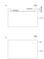
- the light control film 100a shown in FIG. 2A has a substantially rectangular main body 110a exhibiting a light control function and a substantially rectangular shape extending from one side thereof in one direction orthogonal to the thickness direction when viewed from above. It has a first extension 120a and a second extension 120b.
- the first and second extending portions 120a and 120b correspond to the predetermined portion 50, and the first and second extending portions respectively include the first and second transparent electrode layer-attached bases.
- the extraction electrode portion may be formed by removing the material and the liquid crystal light control layer.
- the light control film 100b shown in FIG. 2 (b) has a substantially rectangular shape in a top view, one corner portion being a predetermined portion 50, and the remaining portion being a main body portion 110b. Although not shown, another corner portion that does not overlap with a predetermined portion on the upper surface side in plan view is also a predetermined portion on the lower surface side of the light control film 100b.
- the first base material 10 with a transparent electrode layer includes a first transparent base material 12 and a first transparent base material 12 provided on one side thereof. And a transparent electrode layer 14.
- the first transparent electrode layer-attached substrate 10 is provided on the opposite side of the first transparent substrate 12 on which the first transparent electrode layer 14 is provided and / or on the first transparent substrate 12.
- a first transparent electrode layer 14 may be provided with a hard coat layer.
- an alignment film may be provided on the surface of the transparent electrode layer according to the driving mode.
- the surface resistance of the substrate with the first transparent electrode layer is preferably from 0.1 ⁇ / ⁇ to 1000 ⁇ / ⁇ , more preferably from 0.5 ⁇ / ⁇ to 300 ⁇ / ⁇ , and still more preferably 1 ⁇ / ⁇ . ⁇ 200 ⁇ / ⁇ .
- the haze value of the substrate with the first transparent electrode layer is preferably 20% or less, more preferably 10% or less, and further preferably 0.1% to 10%.
- the total light transmittance of the substrate with the first transparent electrode layer is preferably 30% or more, more preferably 60% or more, and further preferably 80% or more.
- the first transparent electrode layer can be formed using, for example, a metal oxide such as indium tin oxide (ITO), zinc oxide (ZnO), and tin oxide (SnO 2 ).
- the metal oxide may be an amorphous metal oxide or a crystallized metal oxide.
- the crystallized metal oxide has excellent transmittance and electrical conductivity as compared with the amorphous oxide, but is liable to be cracked, and thus is easily cracked or peeled when rubbed with a waste cloth. Therefore, when a transparent electrode layer containing a crystallized metal oxide is used, the effects of the present invention can be more suitably obtained.
- the first transparent electrode layer can also be formed by a metal nanowire such as a silver nanowire (AgNW), a carbon nanotube (CNT), an organic conductive film, a metal layer, or a laminate thereof.
- a metal nanowire such as a silver nanowire (AgNW), a carbon nanotube (CNT), an organic conductive film, a metal layer, or a laminate thereof.
- the first transparent electrode layer may be patterned into a desired shape according to the purpose.
- the thickness of the first transparent electrode layer is preferably 0.01 ⁇ m to 0.10 ⁇ m, and more preferably 0.01 ⁇ m to 0.045 ⁇ m.
- the first transparent electrode layer is provided on one surface of the first transparent base material by, for example, sputtering. After forming a metal oxide layer by sputtering, it can be crystallized by annealing. Annealing is performed, for example, by heat treatment at 120 ° C. to 300 ° C. for 10 minutes to 120 minutes.
- the first transparent substrate can be formed using any appropriate material.
- a forming material a polymer substrate such as a film or a plastics substrate is preferably used.
- the above-mentioned polymer substrate is typically a polymer film mainly containing a thermoplastic resin.
- the thermoplastic resin include a cycloolefin resin such as polynorbornene; an acrylic resin; a polyester resin such as polyethylene terephthalate; a polycarbonate resin; Among them, polynorbornene resin, polyethylene terephthalate resin or polycarbonate resin can be preferably used.
- the above thermoplastic resins may be used alone or in combination of two or more.
- the thickness of the first transparent substrate is preferably 20 ⁇ m to 200 ⁇ m, more preferably 30 ⁇ m to 100 ⁇ m.
- the second substrate with a transparent electrode layer 20 includes a second transparent substrate 22 and a second transparent substrate 22 provided on one side thereof. And a transparent electrode layer 24.
- the second transparent electrode layer-attached substrate 20 is formed on the second transparent substrate 22 on the side opposite to the side on which the second transparent electrode layer 24 is provided and / or on the second transparent substrate 22.
- a second transparent electrode layer 24 may be provided with a hard coat layer.
- an alignment film may be provided on the surface of the transparent electrode layer according to the driving mode.
- the surface resistance of the second substrate with a transparent electrode layer is preferably from 0.1 ⁇ / ⁇ to 1000 ⁇ / ⁇ , more preferably from 0.5 ⁇ / ⁇ to 300 ⁇ / ⁇ , and still more preferably 1 ⁇ / ⁇ . ⁇ 200 ⁇ / ⁇ .
- the haze value of the substrate with the second transparent electrode layer is preferably 20% or less, more preferably 10% or less, and further preferably 0.1% to 10%.
- the total light transmittance of the substrate with the second transparent electrode layer is preferably 30% or more, more preferably 60% or more, and further preferably 80% or more.
- the second transparent electrode layer and the second transparent substrate the same description as the above-mentioned first transparent electrode layer and the first transparent substrate can be applied.
- the second substrate with a transparent electrode layer may have the same configuration as the first substrate with a transparent electrode layer, or may have a different configuration.
- the liquid crystal light control layer 30 typically has a structure in which a liquid crystal compound is dispersed in a resin matrix. Specific examples include a light control layer including a polymer dispersed liquid crystal, a light control layer including a polymer network liquid crystal, and the like.
- the polymer-dispersed liquid crystal has a structure in which liquid crystals are phase-separated in a polymer.
- the polymer network type liquid crystal has a structure in which a liquid crystal is dispersed in a polymer network, and the liquid crystal in the polymer network has a continuous phase.
- any suitable non-polymerized liquid crystal compound is used.
- nematic, smectic, and cholesteric liquid crystal compounds can be used. From the viewpoint of realizing excellent transparency in the transmission mode, it is preferable to use a nematic liquid crystal compound.
- the nematic liquid crystal compound include biphenyl compounds, phenylbenzoate compounds, cyclohexylbenzene compounds, azoxybenzene compounds, azobenzene compounds, azomethine compounds, terphenyl compounds, biphenylbenzoate compounds, and cyclohexylbiphenyl compounds.
- the content ratio of the liquid crystal compound in the liquid crystal light control layer is, for example, 10% by weight or more, preferably 30% by weight or more, more preferably 35% by weight or more, and further preferably 40% by weight or more.
- the content ratio is, for example, 90% by weight or less, preferably 70% by weight or less.
- the resin forming the resin matrix can be appropriately selected according to the light transmittance, the refractive index of the liquid crystal compound, and the like.
- water-soluble resins or water-dispersible resins such as urethane resins, polyvinyl alcohol resins, polyethylene resins, polypropylene resins, and acrylic resins, and liquid crystal polymers, (meth) acrylic resins, silicone resins, and epoxy resins
- radiation-curable resins such as fluorine-based resins, polyester-based resins, and polyimide resins.
- the content ratio of the matrix resin in the liquid crystal light control layer is, for example, 90% by weight or less, preferably 70% by weight or less, more preferably 65% by weight or less, and further preferably 60% by weight or less.
- the content is, for example, 10% by weight or more, preferably 30% by weight or more.
- the matrix resin is crosslinked.
- the crosslinking method is not particularly limited, and examples thereof include a method of adding a crosslinking agent to the matrix resin or a method of polymerizing a crosslinkable matrix resin precursor.
- the crosslinking agent to be added to the matrix resin is not particularly limited, and a thermal crosslinking agent, an ultraviolet crosslinking agent, or the like is selected.
- the amount of the crosslinking agent added to the matrix resin is desirably 0.1 to 10 parts by weight based on 100 parts by weight of the matrix resin.
- the thickness of the liquid crystal light control layer is preferably 2 ⁇ m to 30 ⁇ m, more preferably 3 ⁇ m to 20 ⁇ m, and still more preferably 5 ⁇ m to 15 ⁇ m.
- the liquid crystal light control layer can be manufactured by any appropriate method. As a specific example, an emulsion method and a phase separation method can be given.
- the method for producing the liquid crystal light modulating layer of the emulsion method is, for example, by applying an emulsion coating liquid containing a matrix-forming resin and a liquid crystal compound to the transparent electrode layer surface of the first substrate with a transparent electrode layer. Forming a layer, and drying the coating layer to form a resin matrix on the matrix forming resin.
- the emulsion coating liquid is preferably an emulsion containing a liquid mixture of a matrix forming resin and a coating solvent in a continuous phase and a liquid crystal compound in a dispersed phase.
- a liquid crystal light modulating layer having a configuration in which a liquid crystal compound is dispersed in a resin matrix can be formed.
- a light control film is obtained by laminating a resin substrate with a second transparent electrode layer on the liquid crystal light control layer.
- a method of manufacturing a liquid crystal light control layer of a phase separation method is to apply a coating liquid containing a radiation-curable matrix-forming resin and a liquid crystal compound to a transparent electrode layer surface of a first substrate with a transparent electrode layer.
- Forming a coating layer by laminating a resin substrate with a second transparent electrode layer on the coating layer to form a laminate, and irradiating the laminate with radiation to form a matrix.
- Phase separation of the resin matrix and the liquid crystal compound by polymerizing the resin.
- the coating liquid is preferably in a homogeneous phase.
- a coating liquid is filled between the first transparent electrode layer-attached base material and the second transparent electrode layer-attached substrate stacked via a spacer, and then the phase separation by irradiation is performed. Can be done.
- A-4. Method of Removing Substrate with Transparent Electrode Layer To remove the substrate with a transparent electrode layer, for example, a predetermined portion of the target substrate with a transparent electrode layer is cut with a cutter blade or laser irradiation (so-called, In FIG. 1B, a predetermined portion of the second transparent electrode layer-attached base material is removed by half cutting using a cutter blade.
- a predetermined portion of the substrate with a transparent electrode layer can be removed by peeling off the light control film and breaking it. Typically, all or part of the liquid crystal light control layer remains in a predetermined portion after the base material is removed.
- any appropriate organic solvent capable of swelling the liquid crystal light control layer can be used.
- the organic solvent may dissolve a part of the liquid crystal light control layer when it swells as long as the effects of the present invention can be obtained. It is desirable that the organic solvent does not swell or dissolve the first transparent electrode layer-attached substrate and the second transparent electrode layer-attached substrate.
- Such an organic solvent can be appropriately selected depending on the type and the degree of crosslinking of the matrix forming resin, the material for forming the substrate with a transparent electrode layer, and the like.
- an organic solvent capable of increasing the thickness of the liquid crystal light control layer at the dropped portion is used.
- preferred organic solvents include alcohols (eg, alcohols having 1 to 6 carbon atoms) such as ethanol, isopropyl alcohol, and methanol; ketones such as methyl ethyl ketone, cyclohexanone, and diacetone alcohol; and liquid hydrocarbons such as cyclohexane. And the like.
- alcohols eg, alcohols having 1 to 6 carbon atoms
- ketones such as methyl ethyl ketone, cyclohexanone, and diacetone alcohol
- liquid hydrocarbons such as cyclohexane. And the like.
- the swelling of the liquid crystal light control layer is performed by bringing the organic solvent into contact with the liquid crystal light control layer remaining in the above-mentioned predetermined portion.
- the liquid crystal light control layer can be swollen by dropping or applying an organic solvent to the liquid crystal light control layer, or immersing the light control film in the organic solvent.
- the contact time between the organic solvent and the liquid crystal light control layer can be, for example, 1 second to 60 seconds, preferably 5 seconds to 30 seconds.
- the adhesive tape 300 is attached to the surface of the swollen liquid crystal light control layer 30.
- an adhesive tape is attached so as to cover the entire predetermined portion from which one of the substrates with a transparent electrode layer has been removed.
- the pressure-sensitive adhesive tape 300 typically has a base material 310 and a pressure-sensitive adhesive layer 320 provided on one side thereof.
- the base material examples include polyester (polyethylene terephthalate (PET), polyethylene naphthalate, polybutylene terephthalate, polybutylene naphthalate, etc.), polyolefin (polyethylene, polypropylene (PP), ethylene-propylene copolymer, etc.), polyvinyl Alcohol, polyvinylidene chloride, polyvinyl chloride, vinyl chloride-vinyl acetate copolymer, polyvinyl acetate, polyamide, polyimide, celluloses, fluorine resin, polyether, polyetheramide, polyphenylene sulfide, polystyrene resin (polystyrene etc. ), Plastic base materials such as polycarbonate and polyethersulfone.
- PET polyethylene terephthalate
- PP polypropylene
- PP ethylene-propylene copolymer
- polyvinyl Alcohol polyvinylidene chloride
- polyvinyl chloride vinyl chloride-vin
- the thickness of the substrate is, for example, about 10 ⁇ m to 100 ⁇ m, preferably about 10 ⁇ m to 50 ⁇ m, and more preferably about 10 ⁇ m to 30 ⁇ m.
- the pressure-sensitive adhesive layer preferably does not substantially swell or dissolve in the organic solvent.
- the swollen liquid crystal light control layer and the pressure-sensitive adhesive sheet can be suitably separated from the light control film as a unit.
- the thickness does not substantially change before and after the organic solvent (20 ° C.) is dropped on the surface and left for 30 seconds (for example, the change in the thickness with respect to the thickness before dropping is less than ⁇ 10%) (Preferably within 5%))
- the pressure-sensitive adhesive layer can be preferably used as a pressure-sensitive adhesive layer that does not substantially swell or dissolve in an organic solvent.
- the pressure-sensitive adhesive layer preferably has a gel fraction of 30% to 100%, more preferably a gel fraction of 50% to 90%.
- the gel fraction can be controlled within a desired range by adjusting the degree of crosslinking of the pressure-sensitive adhesive (base polymer) constituting the pressure-sensitive adhesive layer.
- the pressure-sensitive adhesive layer is preferably formed from a pressure-sensitive adhesive composition containing a base polymer and a crosslinking agent.
- a pressure-sensitive adhesive layer having a high gel fraction and not swelling or dissolving in an organic solvent can be suitably obtained.
- the pressure-sensitive adhesive composition may further include any appropriate additive such as a tackifier, a plasticizer, a filler, and an antioxidant.
- the pressure-sensitive adhesive composition can be, for example, an acrylic pressure-sensitive adhesive composition or a rubber-based pressure-sensitive adhesive composition.
- the (meth) acrylic polymer serving as the base polymer of the acrylic pressure-sensitive adhesive is preferably obtained by polymerizing a monomer component containing a (meth) acrylic acid ester having an alkyl group having 2 to 14 carbon atoms. More preferably, it is obtained by polymerizing a monomer component containing a (meth) acrylate having an alkyl group of 2 to 14 as a main monomer.
- the main monomer is preferably 60% by weight or more, and more preferably 70% by weight or more, based on all monomer components constituting the (meth) acrylic polymer.
- (meth) acrylic ester refers to acrylic ester and / or methacrylic ester, and has the same meaning as (meth) in the present invention.
- Examples of the (meth) acrylate having an alkyl group having 2 to 14 carbon atoms include ethyl (meth) acrylate, n-butyl (meth) acrylate, t-butyl (meth) acrylate, and isobutyl (meth) acrylate , Hexyl (meth) acrylate, 2-ethylhexyl (meth) acrylate, n-octyl (meth) acrylate, isooctyl (meth) acrylate, n-nonyl (meth) acrylate, isononyl (meth) acrylate, n-decyl (meth) Acrylate, isodecyl (meth) acrylate, n-dodecyl (meth) acrylate, n-tridecyl (meth) acrylate, n-tetradecyl (meth) acrylate, etc., and these can
- the monomer component may contain other polymerizable monomers other than the (meth) acrylic acid ester having an alkyl group having 2 to 14 carbon atoms.
- the other polymerizable monomer is not particularly limited as long as it has a polymerizable functional group related to an unsaturated double bond such as a (meth) acryloyl group or a vinyl group. Examples include a group-containing monomer.
- hydroxyl group-containing monomer a monomer having a polymerizable functional group having an unsaturated double bond such as a (meth) acryloyl group or a vinyl group and having a hydroxyl group can be used without any particular limitation.
- hydroxyl group-containing monomer examples include 2-hydroxyethyl (meth) acrylate, 3-hydroxypropyl (meth) acrylate, 4-hydroxybutyl (meth) acrylate, 6-hydroxyhexyl (meth) acrylate, and 8-hydroxyoctyl ( (Meth) acrylate, 10-hydroxydecyl (meth) acrylate, 12-hydroxylauryl (meth) acrylate, (4-hydroxymethylcyclohexyl) methyl (meth) acrylate, and the like. Two or more kinds can be used as a mixture.
- the content of the hydroxyl group-containing monomer is preferably 10% by weight or less, more preferably 0 to 5% by weight in the monomer component.
- carboxyl group-containing monomer those having a polymerizable functional group having an unsaturated double bond such as a (meth) acryloyl group or a vinyl group and having a carboxyl group can be used without particular limitation.
- the carboxyl group-containing monomer include acrylic acid, methacrylic acid, carboxyethyl (meth) acrylate, carboxypentyl (meth) acrylate, itaconic acid, maleic acid, fumaric acid, crotonic acid, and the like. These may be used alone or in combination. Can be used.
- the content of the carboxyl group-containing monomer is preferably 10% by weight or less, more preferably 0 to 5% by weight in the monomer component.
- the other copolymerizable monomer is not particularly limited as long as it has a polymerizable functional group related to an unsaturated double bond such as a (meth) acryloyl group or a vinyl group.
- a polymerizable functional group related to an unsaturated double bond such as a (meth) acryloyl group or a vinyl group.
- examples thereof include cyclohexyl (meth) acrylate, (Meth) acrylic alicyclic hydrocarbon esters such as (meth) bornyl acrylate and isobornyl (meth) acrylate; for example, aryl (meth) acrylates such as phenyl (meth) acrylate; for example, vinyl acetate; Vinyl esters such as vinyl propionate; styrene monomers such as styrene; epoxy group-containing monomers such as glycidyl (meth) acrylate and methyl glycidyl (meth) acrylate; acryl
- a cyano group-containing monomer for example, a functional monomer such as 2-methacryloyloxyethyl isocyanate; an olefin-based monomer such as ethylene, propylene, isoprene, butadiene, and isobutylene; a vinyl ether-based monomer such as vinyl ether -;
- a functional monomer such as 2-methacryloyloxyethyl isocyanate
- an olefin-based monomer such as ethylene, propylene, isoprene, butadiene, and isobutylene
- a vinyl ether-based monomer such as vinyl ether -
- monomers containing a halogen atom such as vinyl chloride
- N-vinylcarboxylic acid amides for example, a halogen atom such as vinyl chloride; N-vinylcarboxylic acid amides;
- copolymerizable monomer examples include maleimide monomers such as N-cyclohexylmaleimide, N-isopropylmaleimide, N-laurylmaleimide, and N-phenylmaleimide; for example, N-methylitaconimide, N-ethylitaconimide, -Itaconimide monomers such as -butyl itaconimide, N-octyl itaconimide, N-2-ethylhexyl itaconimide, N-cyclohexyl itaconimide, N-lauryl itaconimide; and N- (meth) acryloyloxymethylene succinimide, N- Succinimide-based monomers such as (meth) acryloyl-6-oxyhexamethylene succinimide and N- (meth) acryloyl-8-oxyoctamethylene succinimide; Sulfonic acid group-containing monomers such as sulf
- Examples of the copolymerizable monomer include glycol-based acrylic ester monomers such as polyethylene glycol (meth) acrylate, polypropylene glycol (meth) acrylate, methoxyethylene glycol (meth) acrylate, and methoxypolypropylene glycol (meth) acrylate. And other examples include heterocyclic rings such as tetrahydrofurfuryl (meth) acrylate and fluorine (meth) acrylate, and acrylate monomers containing a halogen atom.
- glycol-based acrylic ester monomers such as polyethylene glycol (meth) acrylate, polypropylene glycol (meth) acrylate, methoxyethylene glycol (meth) acrylate, and methoxypolypropylene glycol (meth) acrylate.
- heterocyclic rings such as tetrahydrofurfuryl (meth) acrylate and fluorine (meth) acrylate, and acrylate monomers containing
- a polyfunctional monomer can be used as the copolymerizable monomer.
- the polyfunctional monomer include compounds having two or more unsaturated double bonds such as a (meth) acryloyl group and a vinyl group.
- (mono or poly) such as ethylene glycol di (meth) acrylate, diethylene glycol di (meth) acrylate, triethylene glycol di (meth) acrylate, trimethylolpropane tri (meth) acrylate, and tetraethylene glycol di (meth) acrylate
- (Mono or poly) alkylene glycol di (meth) acrylates such as (mono or poly) propylene glycol di (meth) acrylates such as ethylene glycol di (meth) acrylate and propylene glycol di (meth) acrylate, and neopentyl glycol Di (meth) acrylate, 1,6-hexanediol di (meth) acrylate, pentaeryth
- A) acrylate, epoxy (meth) acrylate, urethane (meth) acrylate and the like can also be used.
- the ratio of the copolymerized monomer other than the hydroxyl group-containing monomer and the carboxyl group-containing monomer is preferably 40% by weight or less, more preferably 0 to 30% by weight, and even more preferably 0 to 10% by weight in the monomer component.
- the weight average molecular weight of the (meth) acrylic polymer is preferably 50,000 or more, more preferably 100,000 to 3,000,000, further preferably 500,000 to 2.5 million, and more preferably 1,000,000 to 2,000,000. Is even more preferred.
- the weight average molecular weight refers to a value measured by GPC (gel permeation chromatography) and calculated in terms of polystyrene.
- a polymerization initiator, a chain transfer agent, an emulsifier, and the like used for radical polymerization are not particularly limited, and can be appropriately selected and used.
- the weight average molecular weight of the (meth) acrylic polymer can be controlled by the amount of the polymerization initiator and the amount of the chain transfer agent and the reaction conditions, and the amount is appropriately adjusted according to the type.
- silane coupling agents can be added to the pressure-sensitive adhesive composition to improve adhesion.
- silane coupling agent those having any appropriate functional group can be used.
- the functional group include a vinyl group, an epoxy group, an amino group, a mercapto group, a (meth) acryloxy group, an acetoacetyl group, an isocyanate group, a styryl group, and a polysulfide group.
- vinyl group-containing silane coupling agents such as vinyltriethoxysilane, vinyltripropoxysilane, vinyltriisopropoxysilane, and vinyltributoxysilane; ⁇ -glycidoxypropyltrimethoxysilane, ⁇ -glycol Epoxy group-containing silane coupling agents such as sidoxypropyltriethoxysilane, 3-glycidoxypropylmethyldiethoxysilane, and 2- (3,4-epoxycyclohexyl) ethyltrimethoxysilane; ⁇ -aminopropyltrimethoxysilane; N- ⁇ - (aminoethyl) - ⁇ -aminopropylmethyldimethoxysilane, N- (2-aminoethyl) 3-aminopropylmethyldimethoxysilane, ⁇ -triethoxysilyl-N- (1,3-dimethylbutylidene) Propylamine
- the silane coupling agent may be used alone, or two or more kinds may be used as a mixture.
- the total content is 100 parts by weight of the base polymer (solid content). It is preferably at most 1 part by weight, more preferably from 0.01 to 1 part by weight, even more preferably from 0.02 to 0.8 part by weight.
- the silane coupling agent can be copolymerized with the monomer component by radical polymerization
- the silane coupling agent can be used as the monomer component.
- the ratio is preferably 0.005 to 0.7 parts by weight based on 100 parts by weight of the base polymer (solid content).
- a polyfunctional compound is used, and examples thereof include an organic crosslinking agent and a polyfunctional metal chelate.
- the organic crosslinking agent include an epoxy-based crosslinking agent, an isocyanate-based crosslinking agent, a carbodiimide-based crosslinking agent, an imine-based crosslinking agent, an oxazoline-based crosslinking agent, an aziridine-based crosslinking agent, and a peroxide-based crosslinking agent.
- a polyfunctional metal chelate is one in which a polyvalent metal atom is covalently or coordinated with an organic compound.
- Examples of the polyvalent metal atom include Al, Cr, Zr, Co, Cu, Fe, Ni, V, Zn, In, Ca, Mg, Mn, Y, Ce, Sr, Ba, Mo, La, Sn, and Ti.
- the atom in the organic compound which forms a covalent bond or a coordinate bond includes an oxygen atom and the like, and the organic compound includes an alkyl ester, an alcohol compound, a carboxylic acid compound, an ether compound, a ketone compound and the like.
- These crosslinking agents can be used alone or in combination of two or more. Among these, a peroxide-based crosslinking agent and an isocyanate-based crosslinking agent are preferred, and it is more preferred to use them in combination.
- the isocyanate-based crosslinking agent refers to a compound having two or more isocyanate groups (including an isocyanate regenerating functional group in which isocyanate groups are temporarily protected by a blocking agent or quantification) in one molecule.
- isocyanate-based crosslinking agent examples include aromatic isocyanates such as tolylene diisocyanate and xylene diisocyanate; alicyclic isocyanates such as isophorone diisocyanate; and aliphatic isocyanates such as hexamethylene diisocyanate.
- butylene diisocyanate lower aliphatic polyisocyanates such as hexamethylene diisocyanate, cyclopentylene diisocyanate, cyclohexylene diisocyanate, alicyclic isocyanates such as isophorone diisocyanate, 2,4-tolylene diisocyanate, Aromatic diisocyanates such as 4,4′-diphenylmethane diisocyanate, xylylene diisocyanate, polymethylene polyphenyl isocyanate, and trimethylolpropane / tolylene diisocyanate trimer adduct (trade name: Coronate L, manufactured by Nippon Polyurethane Industry Co., Ltd.) ), Trimethylolpropane / hexamethylene diisocyanate trimer adduct (trade name: Coronate HL, manufactured by Nippon Polyurethane Industry Co., Ltd.), hexamethylene Isocyan
- peroxide-based crosslinking agent di (2-ethylhexyl) peroxy dicarbonate, di (4-t-butylcyclohexyl) peroxy dicarbonate, di-sec-butyl peroxy dicarbonate, t-butyl peroxy neodecanoate , T-hexylperoxypivalate, t-butylperoxypivalate, dilauroyl peroxide, di-n-octanoyl peroxide, 1,1,3,3-tetramethylbutylperoxyisobutyrate, 1 , 1,3,3-tetramethylbutylperoxy 2-ethylhexanoate, di (4-methylbenzoyl) peroxide, dibenzoyl peroxide, t-butylperoxyisobutyrate, and the like. Among them, di (4-t-butylcyclohexyl) peroxy
- the mixing ratio of the crosslinking agent in the pressure-sensitive adhesive composition is not particularly limited, but is generally not more than about 10 parts by weight of the crosslinking agent (solid content) with respect to 100 parts by weight of the base polymer (solid content).
- the mixing ratio of the crosslinking agent is preferably 0.1 to 10 parts by weight, more preferably about 0.5 to 5 parts by weight.
- the base polymer of the rubber-based pressure-sensitive adhesive composition examples include natural rubber and various synthetic rubbers.
- the synthetic rubber examples include polyisoprene rubber, styrene-butadiene (SB) rubber, styrene-isoprene (SI) rubber, styrene-isoprene-styrene block copolymer (SIS) rubber, and styrene-butadiene-styrene block copolymer.
- SBS Combined (SBS) rubber, styrene / ethylene / butylene / styrene block copolymer (SEBS) rubber, styrene / ethylene / propylene / styrene block copolymer (SEPS) rubber, styrene / ethylene / propylene block copolymer (SEP) Examples include rubber, recycled rubber, butyl rubber, polyisobutylene, and modified products thereof.
- SEBS styrene / ethylene / butylene / styrene block copolymer
- SEPS styrene / ethylene / propylene block copolymer
- SEP styrene / ethylene / propylene block copolymer
- the thickness of the pressure-sensitive adhesive layer is, for example, 10 ⁇ m to 50 ⁇ m, preferably 10 ⁇ m to 35 ⁇ m, and more preferably 15 ⁇ m to 30 ⁇ m.
- the 180 ° peeling adhesive strength (relative to polyethylene terephthalate film, peeling temperature: 25 ° C., peeling speed: 300 mm / min) of the adhesive tape is, for example, 1.5 N / 10 mm or more, preferably 2.0 N / 10 mm to 15.0 N /. It is 10 mm, more preferably 3.0 N / 10 mm to 10.0 N / 10 mm.
- the adhesive tape 300 is peeled off from the light control film 100 together with the swollen liquid crystal light control layer 30. Specifically, the liquid crystal light control layer 30 and the adhesive tape 300 whose adhesion to the first transparent electrode layer-attached base material 10 has been reduced due to swelling are collectively peeled off from the light control film 100.
- the peeling method is not particularly limited.
- the peeling speed can be, for example, 0.1 mm / sec to 100 mm / sec, preferably 1 mm / sec to 50 mm / sec.
- the peeling may be performed in a state where the light control film is fixed by a suction table, a suction table, or the like.
- the peeling direction of the adhesive tape is preferably substantially opposite to the extension direction of the extension portion ( 180 ° ⁇ 20 °, preferably 180 ° ⁇ 10 °). By peeling in this direction, the liquid crystal light control layer can be easily peeled and removed while suppressing the load on the substrate with a transparent electrode layer.
- an extraction electrode portion is usually formed for each transparent electrode layer. Therefore, in a predetermined portion on one surface side of the light control film, the above-described steps are performed to remove one of the base material with a transparent electrode layer and the liquid crystal light control layer, and then a predetermined portion on the other surface side.
- the manufacturing method of the present invention may further include, if necessary, after performing a batch removal of the liquid crystal light control layer using an adhesive tape, performing a finish wiping using a rag on the exposed transparent electrode layer. .
- ⁇ Gel fraction> About 0.2 g of the pressure-sensitive adhesive layer was collected from the pressure-sensitive adhesive tape, wrapped in a porous tetrafluoroethylene sheet having an average pore diameter of 0.2 ⁇ m (trade name “NTF1122”, manufactured by Nitto Denko Corporation), and tied with a kite string. was measured (Zg), and the weight was defined as the weight before immersion. The weight before immersion is the total weight of the pressure-sensitive adhesive layer (the pressure-sensitive adhesive layer collected above), the tetrafluoroethylene sheet, and the kite string. The total weight of the tetrafluoroethylene sheet and the kite string was also measured (Yg).
- the adhesive layer was wrapped with a tetrafluoroethylene sheet and tied with a kite string (referred to as “sample”), placed in a 50 mL container filled with ethyl acetate, and allowed to stand at 23 ° C. for 7 days. Thereafter, the sample (after the treatment with ethyl acetate) was taken out of the container, transferred to an aluminum cup, dried in a dryer at 130 ° C. for 2 hours to remove ethyl acetate, and weighed (Xg). The weight was taken as the weight after immersion.
- Example 1 Step of removing substrate with transparent electrode layer (production of first and second substrates with transparent electrode layer) A transparent electrode layer (ITO) was formed on one surface of a cycloolefin-based transparent substrate (a norbornene-based resin film (manufactured by Zeon Corporation, product name “ZF-16”, thickness: 40 ⁇ m, Re [590]: 5 nm)) by sputtering. Layer was formed and annealed at 140 ° C. for 1 hour to form an ITO crystal film (transparent electrode layer) of 100 ⁇ / ⁇ , thus constituting the [cycloolefin-based transparent substrate / transparent electrode layer]. The first and second substrates with a transparent electrode layer having the following were obtained.
- the second substrate with a transparent electrode layer was laminated on the liquid crystal light control layer such that the transparent electrode layer faced the liquid crystal light control layer to obtain a light control film.
- the obtained light control film was punched out with a Thomson blade to obtain a light control film having two extended portions (40 mm ⁇ 20 mm) as shown in FIG.
- Adhesive Tape Adhering Step An adhesive tape of 50 mm ⁇ 30 mm size (thickness of the adhesive layer: 23 ⁇ m, gel fraction of the adhesive layer: 80%) produced by the following method was attached to the swollen liquid crystal light control layer. . At this time, the adhesive tape is adhered so that one long side of the adhesive tape is along the base of the extension (broken line 1) and the other three sides protrude outside the extension. It was made to cover the whole. In addition, this pressure-sensitive adhesive layer did not show swellability and solubility in anhydrous ethanol. The 180 ° peeling adhesive strength of this adhesive tape (based on polyethylene terephthalate film, peeling temperature: 25 ° C, peeling speed: 300 mm / min) was 6 N / 10 mm.
- ⁇ Preparation of adhesive layer> The above pressure-sensitive adhesive composition was applied on a PET film (manufactured by Toyobo Cosmoshine Co., Ltd., product name “A4300”, thickness: 38 ⁇ m), and dried at 140 ° C. for 2 minutes to form a film with a pressure-sensitive adhesive layer having a thickness of 23 ⁇ m. Obtained. Further, the film with the pressure-sensitive adhesive layer was cut into a size of 50 mm ⁇ 30 mm to prepare a pressure-sensitive adhesive tape.
- FIG. 4A shows a scanning electron microscope (SEM) observation image of the formed extraction electrode portion.
- Example 1 In the same manner as in Example 1, a light control film having two extending portions as shown in FIG. 3 was obtained. Only the base material with the transparent electrode layer (base material with the second transparent electrode layer) on the upper surface is cut by a half cutter along the base (broken line 1) of one extension portion, and then the cut second transparent material The substrate with an electrode layer was peeled off. The liquid crystal light control layer remained on the outermost surface of the extension after peeling. A cloth impregnated with anhydrous ethanol was applied to the surface of the liquid crystal light control layer, and the liquid crystal light control layer was reciprocated left and right until the transparent electrode layer of the first substrate with a transparent electrode layer was exposed. As a result, an extraction electrode portion was formed.
- FIG. 4B shows a scanning electron microscope (SEM) observation image of the formed extraction electrode portion.
- the manufacturing method of the present invention is suitable for manufacturing a light control device having a liquid crystal light control layer.
Landscapes
- Physics & Mathematics (AREA)
- Nonlinear Science (AREA)
- Chemical & Material Sciences (AREA)
- Crystallography & Structural Chemistry (AREA)
- General Physics & Mathematics (AREA)
- Optics & Photonics (AREA)
- Mathematical Physics (AREA)
- Dispersion Chemistry (AREA)
- Liquid Crystal (AREA)
- Electroluminescent Light Sources (AREA)
Abstract
Description
1つの実施形態において、上記粘着テープが、上記有機溶媒によって実質的に膨潤または溶解しない粘着剤層を有する。
1つの実施形態において、上記粘着剤層のゲル分率が、30%~100%である。
1つの実施形態において、上記透明電極層が、結晶化金属酸化物を含む。
1つの実施形態において、上記液晶調光層の厚みが、2μm~30μmである。
1つの実施形態において、上記所定の部分が、上記調光フィルムの本体部から厚み方向と直交する方向に延出した延出部であって、上記粘着テープの剥離方向が、該延出部の延出方向と略反対方向である。
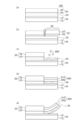
図1(a)~(b)に示すように、透明電極層付基材の除去工程では、透明電極層同士が対向するように配置された第1の透明電極層付基材10および第2の透明電極層付基材20と該透明電極層付基材10、20間に挟持された液晶調光層30とを有する調光フィルム100の所定の部分50において、一方の透明電極層付基材(図示例では、第2の透明電極層付基材20)を除去する。
図1(a)に示されるとおり、第1の透明電極層付基材10は、第1の透明基材12とその一方の側に設けられた第1の透明電極層14とを有する。図示しないが、第1の透明電極層付基材10は、第1の透明基材12の第1の透明電極層14が設けられている側と反対側および/または第1の透明基材12と第1の透明電極層14との間にハードコート層を有していてもよい。また、駆動モードに応じて、透明電極層表面に配向膜が設けられてもよい。
図1(a)に示されるとおり、第2の透明電極層付基材20は、第2の透明基材22とその一方の側に設けられた第2の透明電極層24とを有する。図示しないが、第2の透明電極層付基材20は、第2の透明基材22の第2の透明電極層24が設けられている側と反対側および/または第2の透明基材22と第2の透明電極層24との間にハードコート層を有していてもよい。また、駆動モードに応じて、透明電極層表面に配向膜が設けられてもよい。
液晶調光層30は、代表的には、樹脂マトリクス中に液晶化合物が分散した構造を有する。具体例としては、高分子分散型液晶を含む調光層、高分子ネットワーク型液晶を含む調光層等が挙げられる。高分子分散型液晶は、高分子内において液晶が相分離した構造を有している。高分子ネットワーク型液晶は、高分子ネットワーク中に液晶が分散された構造を有しており、高分子ネットワーク中の液晶は、連続相を有している。
透明電極層付基材の除去は、例えば、カッター刃やレーザー照射によって対象の透明電極層付基材の所定の部分を切断すること(いわゆる、ハーフカット)によって行われる(図1(b)では、カッター刃を用いたハーフカットによって第2の透明電極層付基材の所定の部分の除去が行われている)。また例えば、透明電極層付基材の所定の部分を調光フィルムから剥離し、折り割ることによって除去することができる。代表的には、基材が除去された後の所定の部分には、液晶調光層の全部または一部が残存している。
図1(c)に示すように、液晶調光層の膨潤工程では、上記第2の透明電極層付基材20を除去した後の所定の部分に残存する液晶調光層30を有機溶媒200で膨潤させる。有機溶媒200を用いて液晶調光層30を膨潤させることによって、第1の透明電極層付基材10に対する液晶調光層30の密着強度を低減することができるので、後述の粘着テープの剥離工程において、液晶調光層30を粘着テープと一括して、調光フィルム100から剥離することができる。
図1(d)に示すように、粘着テープの貼付工程においては、膨潤した液晶調光層30の表面に粘着テープ300を貼付する。好ましくは、一方の透明電極層付基材が除去された所定の部分全体を覆うように粘着テープを貼付する。
図1(e)に示すように、粘着テープの剥離工程では、上記粘着テープ300を膨潤した液晶調光層30とともに調光フィルム100から剥離する。具体的には、膨潤により第1の透明電極層付基材10との密着性が低下した液晶調光層30と粘着テープ300とを一括して、調光フィルム100から剥離する。
粘着テープから粘着剤層を約0.2g採取し、平均孔径0.2μmの多孔質テトラフルオロエチレンシート(日東電工社製、商品名「NTF1122」)に包んだ後、凧糸で縛り、その際の重量を測定し(Zg)、該重量を浸漬前重量とした。なお、該浸漬前重量は、粘着剤層(上記で採取した粘着剤層)と、テトラフルオロエチレンシートと、凧糸との総重量である。また、テトラフルオロエチレンシートと凧糸との合計重量も測定した(Yg)。次に、粘着剤層をテトラフルオロエチレンシートで包み、凧糸で縛ったもの(「サンプル」と称する)を、酢酸エチルで満たした50mL容器に入れ、23℃にて7日間静置した。その後、容器からサンプル(酢酸エチル処理後)を取り出して、アルミニウム製カップに移し、130℃で2時間、乾燥機中で乾燥して酢酸エチルを除去した後、重量を測定し(Xg)、該重量を浸漬後重量とした。下記の式からゲル分率を算出した。
ゲル分率(重量%)=(X-Y)/(Z-Y)×100
1.透明電極層付基材の除去工程
(第1および第2の透明電極層付基材の作製)
シクロオレフィン系透明基材(ノルボルネン系樹脂フィルム(日本ゼオン社製、製品名「ZF-16」、厚み:40μm、Re[590]:5nm)の一方の面に、スパッタ法により透明電極層(ITO層)を形成し、140℃で1hrアニールすることによって、100Ω/□のITO結晶膜(透明電極層)を形成した。このようにして、[シクロオレフィン系透明基材/透明電極層]の構成を有する第1および第2の透明電極層付基材を得た。
下記の組成の化合物を150℃で20分混合し、その後室温に徐冷するにより、Δn=0.12、粘度=21cP、Δε=10.1、液晶温度=3~52℃の液晶化合物(1)を得た。

ウレタンエマルション溶液(楠本化成社製、製品名「NeoRez R967」)50部(固形分)に、上記液晶化合物(1)50部を添加し、ホモジナイザーで攪拌することにより、液晶化合物の液滴(平均粒径:5μm)を含むエマルション塗工液を得た。エマルション塗工液を第1の透明電極層付基材の透明電極層側表面に塗布および乾燥させ、これにより、10μm厚の液晶調光層を形成した。
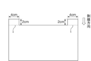
液晶調光層上に、透明電極層が液晶調光層に対向するように第2の透明電極層付基材を積層して、調光フィルムを得た。次いで、得られた調光フィルムをトムソン刃で打ち抜くことにより、図3に示すような2つの延出部(40mm×20mm)を有する調光フィルムを得た。
一方の延出部の付け根(破線1)に沿って上面の透明電極層付基材(第2の透明電極層付基材)のみをハーフカッターにてカットし、その後、カットした第2の透明電極層付基材を剥離除去した。剥離後の延出部の最表面には液晶調光層が残存していた。
上記延出部に残存する液晶調光層の表面に、無水エタノールを含浸させた綿棒をあて、液晶調光層の表面に十分な無水エタノールを付着させた。無水エタノール付着後10秒で、液晶調光層が無水エタノールを吸収し膨潤した。
膨潤した液晶調光層に、下記の方法で作製した50mm×30mmサイズの粘着テープ(粘着剤層の厚み:23μm、粘着剤層のゲル分率:80%)を貼り合わせた。このとき、粘着テープの一方の長辺を延出部の付け根(破線1)に沿わせるとともに、他の三辺が延出部の外方にはみ出るように貼り合わせて、粘着テープが延出部全体を覆うようにした。なお、この粘着剤層は無水エタノールに対して膨潤性および溶解性を示さなかった。また、この粘着テープの180°引き剥がし粘着力(対ポリエチレンテレフタレートフィルム、剥離温度:25℃、剥離速度:300mm/分)は、6N/10mmであった。
<(メタ)アクリル系ポリマーの調製>
冷却管、窒素導入管、温度計および撹拌装置を備えた反応容器にアクリル酸ブチル94部、アクリル酸2-ヒドロキシエチル1部、およびアクリル酸5部を含有するモノマー混合物を仕込んだ。さらに、該モノマー混合物100部に対して、重合開始剤として2,2’-アゾビスイソブチロニトリル0.1部を酢酸エチル100部と共に仕込み、緩やかに攪拌しながら窒素ガスを導入して窒素置換した後、フラスコ内の液温を55℃付近に保って8時間重合反応を行って、重量平均分子量(Mw)180万、Mw/Mn=4.1のアクリル系ポリマーの溶液(固形分濃度30重量%)を調製した。
<粘着剤組成物の調製>
上記で製造したアクリル系ポリマー溶液の固形分100部に対して、ベンゾイルパーオキサイド(日本油脂社製、商品名「ナイパーBMT」)を0.3部、イソシアネート系架橋剤(東ソー社製、商品名「コロネートL」)を1部配合して粘着剤組成物を得た。
<粘着剤層の調製>
上記粘着剤組成物をPETフィルム(東洋紡製コスモシャイン社製、製品名「A4300」、厚み:38μm)上に塗布し、140℃で2分乾燥することにより、厚み23μmの粘着剤層付フィルムを得た。さらに当該粘着剤層付フィルムを50mm×30mmのサイズに裁断して粘着テープを作製した。
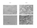
上記貼り合わせの10秒後に、粘着テープを10mm/秒の速さで延出部の延出方向と反対方向に剥離角度180°で剥離したところ、テープ側に膨潤した液晶調光層がすべて転移し、第1の透明電極層付基材の透明電極層が露出した。これにより、取出し電極部が形成された。形成された取出し電極部の走査電子顕微鏡(SEM)観察画像を図4(a)に示す。
実施例1と同様にして、図3に示すような2つの延出部を有する調光フィルムを得た。一方の延出部の付け根(破線1)に沿って上面の透明電極層付基材(第2の透明電極層付基材)のみをハーフカッターにてカットし、その後、カットした第2の透明電極層付基材を剥離除去した。剥離後の延出部の最表面には液晶調光層が残存していた。当該液晶調光層の表面に、無水エタノールを含浸させたウエスをあて、第1の透明電極層付基材の透明電極層が露出するまで、左右に往復して液晶調光層をこすった。これにより、取出し電極部が形成された。形成された取出し電極部の走査電子顕微鏡(SEM)観察画像を図4(b)に示す。
12 第1の透明基材
14 第1の透明電極層
20 第2の透明電極層付基材
22 第2の透明基材
24 第2の透明電極層
30 液晶調光層
100 調光フィルム
300 粘着テープ
Claims (6)
- 透明電極層同士が対向するように配置された第1の透明電極層付基材および第2の透明電極層付基材と該透明電極層付基材間に挟持された液晶調光層とを有する調光フィルムの所定の部分において、一方の透明電極層付基材を除去すること、
該一方の透明電極層付基材を除去した後の該所定の部分に残存する該液晶調光層を有機溶媒で膨潤させること、
該膨潤した液晶調光層の表面に粘着テープを貼付すること、および
該粘着テープを該膨潤した液晶調光層とともに該調光フィルムから剥離すること、を含む、取出し電極部を有する調光素子の製造方法。 - 前記粘着テープが、前記有機溶媒によって実質的に膨潤または溶解しない粘着剤層を有する、請求項1に記載の製造方法。
- 前記粘着剤層のゲル分率が、30%~100%である、請求項2に記載の製造方法。
- 前記透明電極層が、結晶化金属酸化物を含む、請求項1から3のいずれかに記載の製造方法。
- 前記液晶調光層の厚みが、2μm~30μmである、請求項1から4のいずれかに記載の製造方法。
- 前記所定の部分が、前記調光フィルムの本体部から厚み方向と直交する方向に延出した延出部であって、
前記粘着テープの剥離方向が、該延出部の延出方向と略反対方向である、請求項1から5のいずれかに記載の製造方法。
Priority Applications (4)
| Application Number | Priority Date | Filing Date | Title |
|---|---|---|---|
| US17/281,703 US11298930B2 (en) | 2018-10-04 | 2019-09-18 | Method of manufacturing dimming element |
| JP2020550264A JP7332616B2 (ja) | 2018-10-04 | 2019-09-18 | 調光素子の製造方法 |
| CN201980065490.4A CN112789550B (zh) | 2018-10-04 | 2019-09-18 | 调光元件的制造方法 |
| KR1020217009454A KR102785433B1 (ko) | 2018-10-04 | 2019-09-18 | 조광 소자의 제조 방법 |
Applications Claiming Priority (2)
| Application Number | Priority Date | Filing Date | Title |
|---|---|---|---|
| JP2018188917 | 2018-10-04 | ||
| JP2018-188917 | 2018-10-04 |
Publications (1)
| Publication Number | Publication Date |
|---|---|
| WO2020071110A1 true WO2020071110A1 (ja) | 2020-04-09 |
Family
ID=70055902
Family Applications (1)
| Application Number | Title | Priority Date | Filing Date |
|---|---|---|---|
| PCT/JP2019/036446 Ceased WO2020071110A1 (ja) | 2018-10-04 | 2019-09-18 | 調光素子の製造方法 |
Country Status (6)
| Country | Link |
|---|---|
| US (1) | US11298930B2 (ja) |
| JP (1) | JP7332616B2 (ja) |
| KR (1) | KR102785433B1 (ja) |
| CN (1) | CN112789550B (ja) |
| TW (1) | TWI835873B (ja) |
| WO (1) | WO2020071110A1 (ja) |
Cited By (3)
| Publication number | Priority date | Publication date | Assignee | Title |
|---|---|---|---|---|
| EP4036640A4 (en) * | 2020-12-14 | 2022-12-07 | Shanghai Longsheng Photoelectric New Material Co., Ltd. | METHOD OF MANUFACTURING A PDLC MEMBRANE ELECTRODE, A VACUUM PLATFORM AND A PDLC MEMBRANE |
| JP2023135820A (ja) * | 2022-03-16 | 2023-09-29 | 三菱ケミカル株式会社 | 調光シート及び調光シートの製造方法 |
| WO2024048650A1 (ja) * | 2022-09-01 | 2024-03-07 | Toppanホールディングス株式会社 | 調光シート |
Families Citing this family (4)
| Publication number | Priority date | Publication date | Assignee | Title |
|---|---|---|---|---|
| CN113711118B (zh) * | 2019-05-23 | 2024-04-16 | 凸版印刷株式会社 | 调光片以及调光装置 |
| WO2023192117A1 (en) | 2022-03-29 | 2023-10-05 | Nitto Denko Corporation | Polymer matrix with mesogenic ligand and light shutter including the same |
| CN115291444B (zh) * | 2022-09-02 | 2024-03-15 | 上海隆昇光电新材料有限公司 | 分区调光膜、电极制作方法及激光切割装置 |
| KR102829628B1 (ko) * | 2023-08-10 | 2025-07-04 | 주식회사 리비콘 | 고분자 분산 액정 디스플레이의 전극 단자부의 제조방법 |
Citations (2)
| Publication number | Priority date | Publication date | Assignee | Title |
|---|---|---|---|---|
| JP2004069978A (ja) * | 2002-08-06 | 2004-03-04 | Nippon Sheet Glass Co Ltd | 調光体及び合わせガラス |
| JP2009116190A (ja) * | 2007-11-08 | 2009-05-28 | Sharp Corp | 表示パネルの製造方法 |
Family Cites Families (6)
| Publication number | Priority date | Publication date | Assignee | Title |
|---|---|---|---|---|
| JP2003086369A (ja) * | 2001-09-10 | 2003-03-20 | Victor Co Of Japan Ltd | 有機エレクトロルミネセンス素子の製造方法 |
| KR101033797B1 (ko) * | 2003-01-15 | 2011-05-13 | 가부시키가이샤 한도오따이 에네루기 켄큐쇼 | 박리 방법 및 그 박리 방법을 사용한 표시 장치의 제작 방법 |
| JP2012193317A (ja) * | 2011-03-17 | 2012-10-11 | Nitto Denko Corp | 電子部品仮固定用粘着テープ |
| JP2013148687A (ja) | 2012-01-19 | 2013-08-01 | Konica Minolta Inc | 調光フィルム、及び調光フィルムの製造方法 |
| JP2013222846A (ja) * | 2012-04-17 | 2013-10-28 | Nitto Denko Corp | 基板のダイシング方法 |
| US12050385B2 (en) * | 2018-09-10 | 2024-07-30 | Nitto Denko Corporation | Method for manufacturing dimming element |
-
2019
- 2019-09-18 US US17/281,703 patent/US11298930B2/en active Active
- 2019-09-18 WO PCT/JP2019/036446 patent/WO2020071110A1/ja not_active Ceased
- 2019-09-18 CN CN201980065490.4A patent/CN112789550B/zh active Active
- 2019-09-18 KR KR1020217009454A patent/KR102785433B1/ko active Active
- 2019-09-18 JP JP2020550264A patent/JP7332616B2/ja active Active
- 2019-10-01 TW TW108135540A patent/TWI835873B/zh active
Patent Citations (2)
| Publication number | Priority date | Publication date | Assignee | Title |
|---|---|---|---|---|
| JP2004069978A (ja) * | 2002-08-06 | 2004-03-04 | Nippon Sheet Glass Co Ltd | 調光体及び合わせガラス |
| JP2009116190A (ja) * | 2007-11-08 | 2009-05-28 | Sharp Corp | 表示パネルの製造方法 |
Cited By (4)
| Publication number | Priority date | Publication date | Assignee | Title |
|---|---|---|---|---|
| EP4036640A4 (en) * | 2020-12-14 | 2022-12-07 | Shanghai Longsheng Photoelectric New Material Co., Ltd. | METHOD OF MANUFACTURING A PDLC MEMBRANE ELECTRODE, A VACUUM PLATFORM AND A PDLC MEMBRANE |
| US12253767B2 (en) | 2020-12-14 | 2025-03-18 | Shanghai Longsheng Photoelectric New Material Co., Ltd. | Method for manufacturing PDLC membrane electrode, negative pressure platform and PDLC membrane |
| JP2023135820A (ja) * | 2022-03-16 | 2023-09-29 | 三菱ケミカル株式会社 | 調光シート及び調光シートの製造方法 |
| WO2024048650A1 (ja) * | 2022-09-01 | 2024-03-07 | Toppanホールディングス株式会社 | 調光シート |
Also Published As
| Publication number | Publication date |
|---|---|
| JPWO2020071110A1 (ja) | 2021-09-02 |
| CN112789550A (zh) | 2021-05-11 |
| KR102785433B1 (ko) | 2025-03-21 |
| KR20210065954A (ko) | 2021-06-04 |
| JP7332616B2 (ja) | 2023-08-23 |
| US20210394504A1 (en) | 2021-12-23 |
| US11298930B2 (en) | 2022-04-12 |
| TWI835873B (zh) | 2024-03-21 |
| TW202018381A (zh) | 2020-05-16 |
| CN112789550B (zh) | 2024-06-25 |
Similar Documents
| Publication | Publication Date | Title |
|---|---|---|
| JP7332616B2 (ja) | 調光素子の製造方法 | |
| JP6741718B2 (ja) | 粘着剤層、光学フィルムおよび画像表示装置 | |
| JP6378559B2 (ja) | アンカー層形成用組成物、アンカー層、粘着剤層付光学フィルム、及び、画像表示装置 | |
| US9676970B2 (en) | Adhesive agent composition, adhesive agent layer, polarizing plate provided with adhesive agent layer, and image formation device | |
| JP6071224B2 (ja) | 粘着シート | |
| CN113196365B (zh) | 带边框的图像显示面板、以及图像显示装置 | |
| JP6178229B2 (ja) | 液晶パネル、及び画像表示装置 | |
| CN102757752A (zh) | 压敏胶粘剂组合物和压敏胶粘片 | |
| JP6049906B2 (ja) | 粘着剤組成物 | |
| WO2015102086A1 (ja) | アクリル系粘着剤組成物、アクリル系粘着剤層、粘着剤層付き基材フィルム、積層体、及び画像表示装置 | |
| JP2026050373A (ja) | 粘着剤層付偏光フィルム、画像表示パネル及び画像表示装置 | |
| JP2025133763A (ja) | 粘着剤層付光学フィルムおよび該粘着剤層付光学フィルムを含む画像表示装置 | |
| JP6068543B2 (ja) | 液晶パネル及び画像表示装置 | |
| KR102615472B1 (ko) | 점착 필름, 이를 포함하는 광학 부재 및 이를 포함하는 광학표시장치 | |
| JP7515446B2 (ja) | 光学機能層付偏光フィルムおよび液晶表示装置 | |
| CN113168044B (zh) | 图像显示面板、以及图像显示装置 | |
| JP7540874B2 (ja) | 粘着剤層付き偏光フィルム及び画像表示装置 | |
| CN115368853A (zh) | 光学用粘合片 | |
| KR102533838B1 (ko) | 액정 패널 및 액정 표시 장치 | |
| JP2022085457A (ja) | フレキシブルディスプレイ用粘着組成物および粘着シート | |
| KR102621277B1 (ko) | 액정 표시 장치 |
Legal Events
| Date | Code | Title | Description |
|---|---|---|---|
| 121 | Ep: the epo has been informed by wipo that ep was designated in this application |
Ref document number: 19868774 Country of ref document: EP Kind code of ref document: A1 |
|
| ENP | Entry into the national phase |
Ref document number: 2020550264 Country of ref document: JP Kind code of ref document: A |
|
| ENP | Entry into the national phase |
Ref document number: 20217009454 Country of ref document: KR Kind code of ref document: A |
|
| NENP | Non-entry into the national phase |
Ref country code: DE |
|
| 122 | Ep: pct application non-entry in european phase |
Ref document number: 19868774 Country of ref document: EP Kind code of ref document: A1 |