WO2020059010A1 - 制御装置および制御装置の保守方法 - Google Patents
制御装置および制御装置の保守方法 Download PDFInfo
- Publication number
- WO2020059010A1 WO2020059010A1 PCT/JP2018/034415 JP2018034415W WO2020059010A1 WO 2020059010 A1 WO2020059010 A1 WO 2020059010A1 JP 2018034415 W JP2018034415 W JP 2018034415W WO 2020059010 A1 WO2020059010 A1 WO 2020059010A1
- Authority
- WO
- WIPO (PCT)
- Prior art keywords
- semiconductor element
- fixing member
- control device
- heat sink
- screw
- Prior art date
- Legal status (The legal status is an assumption and is not a legal conclusion. Google has not performed a legal analysis and makes no representation as to the accuracy of the status listed.)
- Ceased
Links
Images




Classifications
-
- H—ELECTRICITY
- H05—ELECTRIC TECHNIQUES NOT OTHERWISE PROVIDED FOR
- H05K—PRINTED CIRCUITS; CASINGS OR CONSTRUCTIONAL DETAILS OF ELECTRIC APPARATUS; MANUFACTURE OF ASSEMBLAGES OF ELECTRICAL COMPONENTS
- H05K7/00—Constructional details common to different types of electric apparatus
- H05K7/20—Modifications to facilitate cooling, ventilating, or heating
-
- H—ELECTRICITY
- H10—SEMICONDUCTOR DEVICES; ELECTRIC SOLID-STATE DEVICES NOT OTHERWISE PROVIDED FOR
- H10W—GENERIC PACKAGES, INTERCONNECTIONS, CONNECTORS OR OTHER CONSTRUCTIONAL DETAILS OF DEVICES COVERED BY CLASS H10
- H10W40/00—Arrangements for thermal protection or thermal control
- H10W40/60—Securing means for detachable heating or cooling arrangements, e.g. clamps
-
- H—ELECTRICITY
- H10—SEMICONDUCTOR DEVICES; ELECTRIC SOLID-STATE DEVICES NOT OTHERWISE PROVIDED FOR
- H10W—GENERIC PACKAGES, INTERCONNECTIONS, CONNECTORS OR OTHER CONSTRUCTIONAL DETAILS OF DEVICES COVERED BY CLASS H10
- H10W90/00—Package configurations
Definitions
- the embodiments of the present invention relate to a control device and a maintenance method for the control device.
- heat generated from a semiconductor element mounted on a substrate is radiated by a heat sink formed of an aluminum plate or the like.
- the heat sink fixing screw passed through the screw hole of the substrate is screwed into the mounting hole of the heat sink through a notch or a screw hole provided between both ends of the semiconductor element.
- the distance between the mounting holes of the heat sink corresponds to the distance between the cutouts or the screw holes of the semiconductor element.
- the semiconductor element is fixed to the heat sink by a heat sink fixing screw, and good heat transfer is performed between the two.
- the board may be replaced due to a failure or other factors.
- Semiconductor devices tend to be miniaturized over the years, and newer semiconductor devices have smaller notches or screw holes. Therefore, when the semiconductor element is renewed, it is necessary to change to a heat sink having a dimension between the corresponding mounting holes.
- the heat sink is generally a member fixed to a structural member such as an electrical box, it takes time to remove the heat sink.
- a heat sink must be newly manufactured, which increases costs. Therefore, there is a demand that the board can be replaced without replacing the heat sink. Further, if semiconductor elements having different dimensions can be attached to the same heat sink, the types of heat sinks can be reduced.
- An embodiment of the present invention has been made in view of such circumstances, and provides a control device and a control device maintenance method capable of mounting a substrate on which a different semiconductor element is mounted without replacing a heat sink. With the goal.
- the control device includes a semiconductor element, a substrate on which the semiconductor element is mounted, a heat sink that is in contact with an upper surface of the semiconductor element, a female screw portion formed on the heat sink, A fixing member provided between the lower surface of the element and the substrate; a screw insertion hole formed at a position corresponding to the female screw portion of the fixing member; An engagement portion engaged with the engagement portion; and a screw inserted into the screw insertion hole and screwed into the female screw portion.
- At least two female screw portions are provided on the heat sink at a specific distance, and at least two screw insertion holes are provided on the fixing member at the specific distance.
- the engaged portion is a cutout or a hole for screwing formed in the semiconductor element, and the engaging portion is projected upward from an upper surface of the fixing member. It is a top projection.
- the engaged portion is a side surface of the semiconductor element, and the engaging portion is a peripheral wall protruding upward from a peripheral edge of the fixing member.
- a dimension from an upper surface of the fixing member to an upper end of the peripheral wall portion is smaller than a thickness dimension of the semiconductor element.
- the fixing member is formed of a material having flexibility
- the screw is screwed into the female screw portion
- an upper end of the peripheral wall portion is the upper end of the heat sink. The lower surface is touched.
- the control device includes a lower surface projection projecting downward from a lower surface of the fixing member.
- the control device protrudes upward from a peripheral edge of the fixing member, and protrudes downward from a lower surface of the fixing member, and a peripheral wall portion engaged with the engaged portion of the semiconductor element. And when at least two of the fixing members are stacked, the lower surface projection contacts the inner surface side of the peripheral wall portion.
- the control device includes a connector to which a wiring for leading an alternating current converted by the semiconductor element as an inverter for converting a direct current to an alternating current to the outside of the substrate is connected, and the connector of the fixing member. And an opening that is opened at a position corresponding to.
- the control device includes: an electrical box for housing the board; and a mounting portion formed on the electrical box and to which the heat sink is mounted.
- a maintenance method for a control device includes a step of providing a fixing member between a lower surface of a semiconductor element and a substrate, and a step of forming an engaging portion formed on the fixing member with an engaged portion of the semiconductor element. And mounting the semiconductor element on the substrate; contacting an upper surface of the semiconductor element with a heat sink having a female screw portion; and corresponding to the female screw portion of the fixing member. Inserting a screw into a screw insertion hole formed at a position, and screwing the screw into the female screw portion.
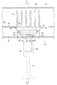
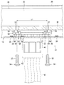
- FIG. 2 is a block diagram illustrating a control device using a semiconductor element. Sectional drawing which shows a heat sink, a fixing member, and a board
- FIG. 3 is an enlarged cross-sectional view showing a semiconductor element and a fixing member before screwing.
- FIG. 5 is an enlarged cross-sectional view showing the semiconductor element and the fixing member after screwing. Sectional drawing which shows the state which laminated
- stacked the fixing member. 9 is a flowchart illustrating a maintenance method of the control device.
- FIG. 4 Note that the upper side of FIG. 4, FIG. 5, FIG. 10, and FIG. 11 will be described as the upper side of the control device.
- an outdoor controller including an inverter device for driving a compressor of an air conditioner will be described as an example.
- 1 is an outdoor unit of an air conditioner.
- the air conditioner includes an outdoor unit 1 installed outdoors and an indoor unit (not shown) installed indoors.
- the outdoor unit 1 and the indoor unit are connected via a refrigerant pipe for circulating a refrigerant.
- a refrigeration cycle is configured by circulating the refrigerant between the outdoor unit 1 and the indoor unit.
- the outdoor unit 1 includes a vertically long box-shaped housing 2.
- the housing 2 has an opening 3 formed in a part of a side surface and a back surface. Further, two upper and lower outlets 4 are opened on the front side of the housing 2, and a mesh-shaped fan guard 5 is provided in these outlets 4.
- the inside of the housing 2 is divided into a heat exchange chamber 7 and a machine room 8 by a partition plate 6.
- the heat exchanger 9 is provided with a heat exchanger 9, and two upper and lower blowers 10 are provided in front of the heat exchanger 9.
- Each of the blowers 10 is provided at a position corresponding to the two fan guards 5 on the front side of the housing 2.
- the blower 10 includes a fan motor 11 and a propeller-type fan 12 attached to a rotation shaft of the fan motor 11. By driving the fan motor 11, the fan 12 is rotated. Then, air flows in from the opening 3 of the housing 2, heat exchange is performed between the air and the refrigerant flowing inside the heat exchanger 9, and the air after the heat exchange is blown with the fan guard 5 attached. It is blown out from the outlet 4.
- the machine room 8 is provided with a compressor 13 for compressing gaseous refrigerant, an accumulator 14 for storing liquid refrigerant, and a four-way valve 15 for switching the flow of the refrigerant in the refrigerant pipe.
- an electrical box 16 is provided in the machine room 8.
- the electrical equipment box 16 houses a control device 17 which is an outdoor controller including an inverter device for supplying power to various devices such as the fan motor 11 and the compressor 13 and performing control.
- the inverter device is a device that converts DC into AC.
- a printed circuit board 18 (hereinafter, referred to as a board 18) constituting the control device 17 is accommodated in the housing 26 of the electrical component box 16.
- a semiconductor element 21 as an electronic component is mounted on the substrate 18.
- the substrate 18 has a plurality of semiconductor elements 21 and various electric and electronic components mounted thereon.
- a control circuit for controlling the fan motor 11 and the compressor 13 is configured by these components.
- the circuit of the control device 17 includes, as heating elements, a first semiconductor element 21A which is a switching element IGBT constituting a power factor correction circuit and a second semiconductor element which is a three-phase inverter (IPM) connected to the compressor 13. 21B, a third semiconductor element 21C that is a three-phase inverter (IPM) connected to one fan motor 11, and a fourth semiconductor element 21D that is a three-phase inverter (IPM) connected to the other fan motor 11.
- a first semiconductor element 21A which is a switching element IGBT constituting a power factor correction circuit
- IPM three-phase inverter
- a fifth semiconductor element 21E which is a full-wave rectifier circuit connected to the AC power supply 22, and a sixth semiconductor element 21F, which is also a full-wave rectifier circuit connected to the AC power supply 22, are provided.
- the first to sixth semiconductor elements 21A to 21F may be collectively referred to as a semiconductor element 21.
- IGBT In the first semiconductor element 21A, only a single IGBT element is housed in the package.
- IPM In the second to fourth semiconductor elements 21B to 21D (IPM), six switching elements such as IGBTs forming an inverter and a circuit for driving the switching elements are housed in one package.
- the element that generates the largest amount of heat is the second semiconductor element 21B that switches a large current for driving the compressor 13 by PWM (Pulse Width Modulation).
- the control unit 23 is connected to each of the first semiconductor element 21A, the second semiconductor element 21B, the third semiconductor element 21C, and the fourth semiconductor element 21D, and controls the operation of each element.
- the switching of each element is controlled by the control unit 23, and the compressor 13 and the two fan motors 11 are driven at a variable speed.
- the control unit 23 includes a microcomputer and its peripheral circuits, and these circuits and elements are also mounted on the board 18.
- the fifth semiconductor element 21E and the sixth semiconductor element 21F are connected to the AC power supply 22 via the inductor 20. Further, the DC rectified by the sixth semiconductor element 21F is supplied to the second semiconductor element 21B, the third semiconductor element 21C, and the fourth semiconductor element 21D via the capacitor 19.
- the first semiconductor element 21A is turned on / off once or a plurality of times at a specific timing of the half-wave of the sine wave of the AC power supply 22, thereby bringing the current from the AC power supply 22 closer to the sine wave and improving the power factor.
- a power factor improving circuit (high power factor circuit) is configured. Since the first semiconductor element 21A needs to be turned ON / OFF at both the positive half-wave and the negative half-wave, the AC power supply 22 is provided by the full-wave rectifier circuit of the fifth semiconductor element 21E provided on the input side. The input from is rectified.
- the housing 26 of the electrical component box 16 is formed using sheet metal.
- the electrical component box 16 is provided with a heat sink 24 for cooling the semiconductor element 21 to be mounted.
- the heat sink 24 is mounted on a mounting portion 27 formed on a housing 26 of the electrical component box 16 formed of a member such as a sheet metal.
- the mounting portion 27 is an opening that allows the heat sink 24 to protrude from the inside of the housing 26 to the outside.
- a holding piece 28 for holding the heat sink 24 to the housing 26 is provided at an edge of the mounting portion 27.
- the length and width of the mounting portion 27 are formed so as to match the length and width of the heat sink 24. That is, the heat sink 24 and the holding piece 28 are watertightly fixed by a fastening member such as a screw (not shown) so that there is no gap between the heatsink 24 and the holding piece 28, so that water droplets from the outside do not enter the inside of the housing 26.
- the board 18 to which various electric and electronic components are soldered is fixed to a predetermined portion of the housing 26.
- the semiconductor element 21 mounted on the substrate 18 includes a package 29 for housing a semiconductor chip.
- a plurality of terminals 30 protruding from the side surface of the package 29 are soldered to the substrate 18.
- the shape of the package 29 is a rectangular flat plate in plan view (see FIG. 6). Terminals 30 are provided on two side surfaces in the longitudinal direction among the four side surfaces of the package 29, and cutout portions 32 for fixing the semiconductor element 21 to the heat sink 24 by screws are formed on the two side surfaces 31 in the short direction. Have been.
- the fixing member 50 is provided between the lower surface of the semiconductor element 21 and the upper surface of the substrate 18.
- the semiconductor element 21 is attached to the heat sink 24 with two screws 33 via the fixing member 50.
- the notch 32 for screwing provided in the semiconductor element 21 described above is not used for screwing.
- Each screw 33 is provided with a washer 34 for locking the screw head to the lower surface of the fixing member 50.
- the fixing member 50 is a member formed of a flexible material such as a synthetic resin. By doing so, the productivity of the fixing member 50 can be improved.
- the lower surface of the base 35 of the heat sink 24 comes into close contact with the upper surface of the semiconductor element 21 fixed by the screw 33.
- the heat sink 24 is provided with a plurality of fins 25 protruding to the outside of the housing 26.
- the heat sink 24 is a member formed of a metal having a high heat transfer coefficient, such as aluminum. Heat generated from the semiconductor element 21 is released to the outside by the heat sink 24 to prevent the temperature of the semiconductor element 21 from rising.
- the shape and dimensions of the fins 25 are such that they do not interfere with other constituent members 36 constituting the outdoor unit 1, for example, the housing 2 on the rear side of the outdoor unit 1. That is, the shape and the projection size of the fin 25 are set according to the configuration of the outdoor unit 1.
- the heat sink 24 is formed with two female screw portions 37 provided at a specific distance L1.
- the above-mentioned screw 33 is screwed into these female screw portions 37.
- the female screw portion 37 vertically passes through the base 35 of the heat sink 24. Since the female screw portion 37 of the heat sink 24 penetrates to the outside, it is necessary to securely close it with the screw 33 in order to prevent rainwater from entering the housing 26.
- Two female screw portions 37 are provided for each semiconductor element 21. That is, when a plurality of semiconductor elements 21 are provided, twice as many female screw portions 37 as the number of semiconductor elements 21 are formed on the heat sink 24.
- the substrate 18 has two large holes 38 having openings larger than the screw head of the screw 33 and the washer 34. These large holes 38 are provided at positions corresponding to the respective female screw portions 37 of the heat sink 24.
- a minute electronic component 39 such as a resistor is provided on the upper surface of the substrate 18. Further, on the lower surface of the board 18, a connector 40 for outputting the alternating current converted by the semiconductor element 21 as an inverter device is provided on the lower surface of the board 18.
- the connector 40 is provided corresponding to a mounting position of the semiconductor element 21.
- a terminal 42 of a wiring 41 for leading the alternating current converted by the semiconductor element 21 to the outside of the substrate 18 is connected.
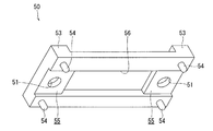
- the fixing member 50 has a rectangular (rectangular) flat plate shape in plan view.
- the fixing member 50 has at least two screw insertion holes 51 provided at a specific distance L2.
- the specific distance L2 between the two screw insertion holes 51 of the fixing member 50 is the same as the specific distance L1 between the two female screw portions 37 of the heat sink 24 (see FIG. 5). That is, the screw insertion hole 51 is provided at a position corresponding to the female screw portion 37.
- the screw 33 is inserted into the screw insertion hole 51 from the lower surface side of the fixing member 50 and screwed into the female screw portion 37 of the heat sink 24.
- the notch 32 of the semiconductor element 21 has a shape obtained by cutting out the lateral side 31 of the semiconductor element 21 in a semicircular shape.
- the separation distance L3 between the two notches 32 is shorter than the specific distances L1 and L2.
- the intended use of the notch 32 is to fix the semiconductor element 21 to the heat sink 24 by inserting a screw 33 into the notch 32.
- the specific distance L1 between the female screw portions 37 of the heat sink 24 matches the separation distance L3 between the cutout portions 32.
- the distance L3 between the notches 32 of the new type semiconductor element 21 is smaller than the distance L3 between the notches 32 of the old type semiconductor element 21. That is, the separation distance L3 between the notches 32 of the new type semiconductor element 21 does not match the specific distance L1 between the female threads 37 of the heat sink 24.
- the substrate 18 or the old-type semiconductor element 21 breaks down due to long-term use and the outdoor unit 1 needs to be repaired, it may be difficult to obtain the old-type semiconductor element 21 already. In this case, the substrate 18 is newly manufactured using the new semiconductor element 21.
- the female screw 37 does not fit in the notch 32 of the new semiconductor element 21 and cannot be attached to the heat sink 24 that fits the old semiconductor element 21.
- the heat sink 24 is fixed to the casing 26 of the electrical box 16, and the casing 26 is fixed to the casing 2 of the outdoor unit 1.
- the original heat sink 24 is removed and a new heat sink 24 is attached.
- the fixing member 50 by using the fixing member 50, the small-sized new semiconductor element 21 is attached to the heat sink 24 manufactured according to the old semiconductor element 21. In this way, it is possible to replace the heat sink 24 with the substrate 18 on which the new semiconductor element 21 is mounted without replacing the heat sink 24. Since the fixing member 50 is formed of a synthetic resin, the fixing member 50 can be easily newly formed in accordance with the size of the new semiconductor element 21.
- the fixing member 50 has a frame shape as a whole and includes two upper surface protrusions 52 protruding upward from the upper surface thereof. These upper surface protruding portions 52 have a columnar shape having a notch in a part in plan view. Each upper surface projection 52 is engaged with the cutout 32 of the package 29 of the semiconductor element 21. That is, the notch 32 is an engaged portion with which the upper surface projection 52 as the engaging portion is engaged.
- the upper surface projection 52 of the fixing member 50 is engaged with the notch 32 of the semiconductor element 21, so that the semiconductor element 21 can be positioned.
- the semiconductor element 21 is prevented from wobbling in the horizontal direction (horizontal direction in FIG. 6) and the vertical direction (vertical direction in FIG. 6).
- the cylindrical shape of the upper surface protruding portion 52 may have a shape narrowing upward. In this way, when the semiconductor element 21 is placed on the fixing member 50 from above, the upper projection 52 can be easily engaged with the notch 32.
- the fixing member 50 includes two peripheral wall portions 53 protruding upward from the peripheral edge. These peripheral wall portions 53 are provided corresponding to the two side surfaces 31 of the semiconductor element 21 where the terminals 30 are not provided. Each peripheral wall 53 has a U-shape in plan view, and its end is engaged with the side surface 31 of the package 29 of the semiconductor element 21. That is, the side surface 31 of the semiconductor element 21 of the present embodiment is an engaged portion with which the peripheral wall portion 53 as the engaging portion is engaged.
- the semiconductor element 21 can be positioned.
- the semiconductor element 21 does not wobble in the horizontal direction (the left-right direction in FIG. 6).
- the semiconductor element 21 can be fixed by the peripheral wall portion 53 so as not to shake. Note that the protrusion dimension of the peripheral wall 53 is larger than the protrusion dimension of the upper surface protrusion 52.
- the fixing member 50 includes four lower surface protrusions 54 protruding downward from the lower surface thereof.
- the respective lower surface projections 54 are provided at four corners of the lower surface of the fixing member 50. These lower surface projections 54 come into contact with the upper surface of the substrate 18. By doing so, a space is provided between the lower surface of the fixing member 50 and the upper surface of the substrate 18, so that the fixing member 50 does not interfere with the minute electronic components 39 provided on the substrate 18 (FIG. 5). reference).
- a lower surface of the fixing member 50 is provided with two washer surfaces 55 on which the screw head of the screw 33 and the washer 34 are hooked. These washer surfaces 55 are provided at positions higher than other portions of the lower surface of the fixing member 50. This prevents the screw head of the screw 33 from interfering with the minute electronic component 39 provided on the substrate 18.
- an opening 56 having a quadrangular (rectangular) shape in plan view is opened in the center of the fixing member 50.
- the opening 56 is provided at a position corresponding to the connector 40.
- the fixing member 50 can be prevented from interfering with the connector 40 to which a high voltage is applied.
- the fixing member 50 can be formed using a general-purpose resin material. That is, since it is possible to speak the distance with the high voltage portion, it is not necessary to use a high tracking resistance material, and the fixing member 50 can be manufactured at low cost.
- the fixing member 50 is formed by providing a difference D (minus error) between the protrusion dimension T1 of the peripheral wall portion 53 and the thickness dimension T2 of the semiconductor element 21. This allows the upper surface of the semiconductor element 21 to be in close contact with the lower surface of the heat sink 24.
- the upper end of the peripheral wall portion 53 contacts the lower surface of the heat sink 24. That is, when the screw 33 is screwed into the female screw portion 37 of the heat sink 24, the fixing member 50 is warped by the tightening force, and the upper end of the peripheral wall portion 53 contacts the lower surface of the heat sink 24. Even if the screw 33 is tightened, the upper end of the peripheral wall 53 is in contact with the lower surface of the heat sink 24, so that the load applied to the fixing member 50 can be suppressed.
- the fixing member 50 when the fixing member 50 is transported as a component, the plurality of fixing members 50 are packed in a stacked state.
- the fixing member 50 is provided at a position where the lower surface projection 54 abuts on the inner surface side of the lower peripheral wall portion 53 when a plurality of fixing members 50 are stacked vertically. This prevents the fixing members 50 from wobbling in the horizontal direction (the horizontal direction in FIG. 12) during the conveyance.
- the screw insertion hole 51 of the fixing member 50 corresponds to the female screw portion 37 of the heat sink 24. 24.
- the female screw portions 37 formed at a plurality of positions of the heat sink 24 are closed by screwing the screws 33. Therefore, water droplets are prevented from entering the inside of the housing 26 from these female screw portions 37. Further, only the number of female screw portions 37 corresponding to the semiconductor element 21 to be attached is formed on the heat sink 24. Therefore, all the female screw portions 37 are closed by the screws 33.
- the board 18 can be replaced while the heat sink 24 is mounted on the mounting portion 27 of the electrical component box 16, so that the heat sink 24 does not need to be newly manufactured. That is, the old heat sink 24 can be used.
- the fixing member 50 is not fixed to the substrate 18, it is not necessary to strictly control the dimensions of the fixing member 50. Therefore, the manufacturability of the fixing member 50 can be improved.
- Steps S11 to S13 in FIG. 13 correspond to a method of manufacturing the substrate 18, and steps S14 to S13 correspond to a method of replacing the control device 17, which will be described together as a maintenance method of the control device 17.
- step S11 when manufacturing a new board 18 for maintenance, the manufacturer attaches the fixing member 50 to the new board 18 as a temporary fix. For example, a pin of a predetermined jig is inserted into the large hole 38 from below the new substrate 18, and the pin of this jig is inserted into the screw insertion hole 51 of the fixing member 50. By doing so, the fixing member 50 is positioned by the pins of the jig.
- the manufacturer places the new semiconductor element 21 on the upper surface of the fixing member 50.
- the upper surface protruding portion 52 as the engaging portion of the fixing member 50 is engaged with the notch 32 as the engaged portion of the semiconductor element 21.
- the peripheral wall portion 53 as the engaging portion of the fixing member 50 is engaged with the side surface 31 as the engaged portion of the semiconductor element 21.
- the manufacturer mounts the semiconductor element 21 on a new substrate 18. That is, the terminals 30 of the semiconductor element 21 are soldered to the substrate 18. After this soldering, the predetermined jig is removed from the new substrate 18.
- the worker starts maintenance work of the outdoor unit 1.
- the operator removes the old board 18 from the electrical box 16.
- the fixing member 50 is not provided on the old substrate 18, and the semiconductor element 21 is directly screwed to the heat sink 24 via the notch 32. Therefore, first, the screw 33 fixing the semiconductor element 21 is removed. Thereafter, the old substrate 18 is removed.
- the heat sink 24 is maintained in a state of being attached to the electrical box 16.
- step S15 the operator accommodates a new board 18 for maintenance in the electrical box 16. That is, a new board 18 is attached to the electrical box 16.
- the worker attaches the new board 18 to the electrical component box 16 so that the upper face of the semiconductor element 21 contacts the lower face of the heat sink 24.
- step S17 the operator inserts the screw 33 from below the new substrate 18 through the large hole 38. Then, the screw 33 is inserted into the screw insertion hole 51 of the fixing member 50.
- step S18 the operator screws the screw 33 inserted into the screw insertion hole 51 into the female screw portion 37 of the heat sink 24. Then, the maintenance work of the outdoor unit 1 ends.
- two female screw portions 37 are formed in the heat sink 24 and two screw insertion holes 51 are formed in the fixing member 50.
- the number of screw insertion holes 51 formed in the fixing member 50 may be one. Then, one end of the semiconductor element 21 is fixed by inserting the screw 33 into one screw insertion hole 51 of the fixing member 50, and the other end is fixed by inserting the screw 33 into the notch 32 at the other end of the semiconductor element 21. You may. That is, the fixing member 50 only needs to be provided with at least one screw insertion hole 51 apart from the notch 32 of the semiconductor element 21.
- holes for screwing may be provided at both ends in the longitudinal direction instead of the cutouts 32 on the side surfaces 31.
- a screw hole may be used as the engaged portion.
- a substrate on which a different semiconductor element is mounted can be attached without replacing a heat sink. Furthermore, according to the present embodiment, not only the repair parts but also a board in which semiconductor elements of different dimensions are mounted on the same heat sink at the manufacturing stage can be used together.
Landscapes
- Physics & Mathematics (AREA)
- Thermal Sciences (AREA)
- Engineering & Computer Science (AREA)
- Microelectronics & Electronic Packaging (AREA)
- Cooling Or The Like Of Electrical Apparatus (AREA)
- Cooling Or The Like Of Semiconductors Or Solid State Devices (AREA)
Abstract
制御装置(17)は、半導体素子(21)と、半導体素子(21)が搭載される基板(18)と、半導体素子(21)の上面に接触されるヒートシンク(24)と、ヒートシンク(24)に形成された雌ネジ部(37)と、半導体素子(21)の下面と基板(18)との間に設けられる固定部材(50)と、固定部材(50)の雌ネジ部(37)に対応する位置に形成されたネジ挿通孔(51)と、固定部材(50)に形成され、半導体素子(21)の被係合部(32)に係合される係合部(52)と、ネジ挿通孔(51)に挿通され、雌ネジ部(37)に螺合されるネジ(33)を備える。
Description
本発明の実施形態は、制御装置および制御装置の保守方法に関する。
従来、電源回路またはインバータ装置などの制御装置では、基板に搭載される半導体素子から発生する熱をアルミ板等で成形されたヒートシンクにより放熱させている。このような制御装置では、基板のネジ用穴に通されたヒートシンク固定用ネジを、半導体素子の両端間に設けられた切り欠きまたはネジ穴を介してヒートシンクの取り付け穴に螺合させている。このヒートシンクの取り付け穴同士の離間寸法は、半導体素子の切り欠きまたはネジ穴同士の離間寸法に対応している。そして、半導体素子がヒートシンク固定用ネジによりヒートシンクに固定され、両者間で良好な熱伝達が行われるようになっている。
故障などの要因により基板を交換することがある。半導体素子は年を追って小型化される傾向があり、新型の半導体素子は切り欠きまたはネジ穴同士の離間寸法が小さくなる。そのため、半導体素子が更新される場合には、これに対応した取り付け穴間の寸法を持つヒートシンクに変更しなければならない。ところが、ヒートシンクは一般に電装箱などの構造部材に固定される部材であるため、その取外作業に手間がかかる。また、ヒートシンクを新造しなければならずコストが嵩む。そこで、ヒートシンクを交換せずに基板の交換が行えるようにしたいという要望がある。また、同じヒートシンクに異なる寸法の半導体素子を取り付けることができればヒートシンクの種類を削減することもできる。
本発明の実施形態は、このような事情を考慮してなされたもので、ヒートシンクを交換することなく異なる半導体素子を搭載した基板を取り付けることができる制御装置および制御装置の保守方法を提供することを目的とする。
本発明の実施形態に係る制御装置は、半導体素子と、前記半導体素子が搭載される基板と、前記半導体素子の上面に接触されるヒートシンクと、前記ヒートシンクに形成された雌ネジ部と、前記半導体素子の下面と前記基板との間に設けられる固定部材と、前記固定部材の前記雌ネジ部に対応する位置に形成されたネジ挿通孔と、前記固定部材に形成され、前記半導体素子の被係合部に係合される係合部と、前記ネジ挿通孔に挿通され、前記雌ネジ部に螺合されるネジと、を備える。
本発明の実施形態に係る制御装置において、少なくとも2つの前記雌ネジ部が特定距離を空けて前記ヒートシンクに設けられ、かつ少なくとも2つの前記ネジ挿通孔が前記特定距離を空けて前記固定部材に設けられる。
本発明の実施形態に係る制御装置において、前記被係合部が前記半導体素子に形成されたネジ止め用の切欠部または穴であり、前記係合部が前記固定部材の上面から上方に突出される上面突起部である。
本発明の実施形態に係る制御装置において、前記被係合部が前記半導体素子の側面であり、前記係合部が前記固定部材の周縁から上方に突出される周縁壁部である。
本発明の実施形態に係る制御装置において、前記固定部材の上面から前記周縁壁部の上端までの寸法が、前記半導体素子の厚み寸法よりも小さい。
本発明の実施形態に係る制御装置において、前記固定部材が可撓性を有する材質で形成され、前記ネジが前記雌ネジ部に螺合されたときに、前記周縁壁部の上端が前記ヒートシンクの下面に接触される。
本発明の実施形態に係る制御装置は、前記固定部材の下面から下方に突出される下面突起部を備える。
本発明の実施形態に係る制御装置は、前記固定部材の周縁から上方に突出され、前記半導体素子の被係合部に係合される周縁壁部と、前記固定部材の下面から下方に突出される下面突起部と、を備え、少なくとも2つの前記固定部材が積み重ねられたときに、前記下面突起部が前記周縁壁部の内面側に接触される。
本発明の実施形態に係る制御装置は、直流を交流に変換するインバータとしての前記半導体素子で変換された交流を前記基板の外部に導出する配線が接続されるコネクタと、前記固定部材の前記コネクタに対応する位置に開口された開口部と、を備える。
本発明の実施形態に係る制御装置は、前記基板を収容する電装箱と、前記電装箱に形成され、前記ヒートシンクが取り付けられる取付部と、を備える。
本発明の実施形態に係る制御装置の保守方法は、半導体素子の下面と基板との間に固定部材を設けるステップと、前記固定部材に形成された係合部を前記半導体素子の被係合部に係合するステップと、前記半導体素子を前記基板に搭載するステップと、雌ネジ部が形成されたヒートシンクに前記半導体素子の上面を接触させるステップと、前記固定部材の前記雌ネジ部に対応する位置に形成されたネジ挿通孔にネジを挿通するステップと、前記ネジを前記雌ネジ部に螺合するステップと、を含む。
以下、図面を参照しながら、制御装置および制御装置の保守方法の実施形態について詳細に説明する。なお、図4、図5、図10および図11の紙面上側を制御装置の上側として説明する。
本実施形態の制御装置として、空気調和機の圧縮機を駆動するインバータ装置を含む室外制御器を例にとって説明する。図1の符号1は、空気調和機の室外機である。空気調和機は、室外に設置される室外機1と室内に設置される室内機(図示略)とで構成される。室外機1と室内機とは、冷媒を循環させる冷媒配管を介して接続されている。そして、室外機1と室内機との間で冷媒を循環させることで冷凍サイクルが構成される。
図1に示すように、室外機1は、縦長の箱状を成す筐体2を備える。この筐体2には、側面と背面の一部に開口部3が形成されている。また、筐体2の正面側には、上下2つの吹出口4が開口され、これらの吹出口4に網目状のファンガード5が設けられている。
図2に示すように、筐体2の内部は、仕切板6により熱交換室7と機械室8とに分けられている。熱交換室7には、熱交換器9が設けられるとともに、この熱交換器9の前方に上下2つの送風機10が設けられている。この送風機10は、それぞれが、筐体2の正面側の2つのファンガード5に対応する位置に設けられている。
送風機10は、ファンモータ11と、このファンモータ11の回転軸に取り付けられたプロペラ型のファン12から成る。ファンモータ11を駆動させることで、ファン12が回転される。そして、筐体2の開口部3から空気が流れ込み、この空気と熱交換器9の内部を流れる冷媒との間で熱交換が行われ、熱交換後の空気がファンガード5の取り付けられた吹出口4から吹き出されるようになっている。
機械室8には、ガス状の冷媒を圧縮する圧縮機13と、液冷媒を貯めるアキュムレータ14と、冷媒配管の冷媒の流れを切り換える四方弁15とが設けられている。さらに、機械室8には、電装箱16が設けられている。この電装箱16には、ファンモータ11および圧縮機13などの各種機器に電力を供給するとともに制御を行うためのインバータ装置を含む室外制御器である制御装置17が収容されている。なお、インバータ装置は、直流を交流に変換する装置である。
図4および図5に示すように、電装箱16の筐体26の内部には、制御装置17を構成するプリント回路基板18(以下、基板18という。)が収容されている。この基板18には、電子部品である半導体素子21が搭載されている。なお、基板18には、複数の半導体素子21、さらには様々な電気・電子部品が搭載されている。これらの部品によりファンモータ11および圧縮機13を制御する制御回路が構成されている。
次に、制御装置17の回路構成を図3に示すブロック図を参照して説明する。制御装置17の回路には、発熱素子として、力率改善回路を構成するスイッチング素子IGBTである第1半導体素子21Aと、圧縮機13に接続される三相インバータ(IPM)である第2半導体素子21Bと、一方のファンモータ11に接続される三相インバータ(IPM)である第3半導体素子21Cと、他方のファンモータ11に接続される三相インバータ(IPM)である第4半導体素子21Dと、交流電源22に接続される全波整流回路である第5半導体素子21Eと、同じく交流電源22に接続される全波整流回路である第6半導体素子21Fが設けられる。以下、第1半導体素子21Aないし第6半導体素子21Fを総称して半導体素子21と呼ぶ場合がある。
第1半導体素子21Aは、IGBTの単一素子のみがパッケージに収納される。第2半導体素子21Bないし第4半導体素子21D(IPM)は、インバータを構成する6つのIGBTなどのスイッチング素子と、これを駆動する回路が1つのパッケージに収納される。
なお、これらの半導体素子21の中で、最も発熱量の大きい素子は、圧縮機13を駆動するための大電流をPWM(Pulse Width Modulation)でスイッチングする第2半導体素子21Bである。
また、第1半導体素子21Aと第2半導体素子21Bと第3半導体素子21Cと第4半導体素子21Dとのそれぞれに接続され、各素子の動作を制御する制御部23が設けられている。この制御部23により各素子のスイッチングが制御されて、圧縮機13および2つのファンモータ11が可変速駆動される。なお、制御部23は、マイクロコンピュータおよびその周辺回路からなり、これらの回路および素子も基板18に搭載されている。
第5半導体素子21Eおよび第6半導体素子21Fは、インダクタ20を介して交流電源22に接続される。さらに、第6半導体素子21Fで整流された直流がコンデンサ19を介して、第2半導体素子21Bと第3半導体素子21Cと第4半導体素子21Dに供給される。
また、第1半導体素子21Aは、交流電源22の正弦波の半波の特定タイミングで1回若しくは複数回ON/OFFすることで、交流電源22からの電流を正弦波に近づけて力率を向上させる力率改善回路(高力率回路)を構成する。この第1半導体素子21Aは、正の半波と負の半波の両方でON/OFFする必要があるため、その入力側に設けられた第5半導体素子21Eの全波整流回路によって交流電源22からの入力を整流している。
図4および図5に示すように、電装箱16の筐体26は、板金を用いて形成されている。この電装箱16には、実装される半導体素子21を冷却するためのヒートシンク24が設けられる。ヒートシンク24は、板金などの部材で形成される電装箱16の筐体26に形成された取付部27に取り付けられている。
取付部27は、ヒートシンク24を筐体26の内部から外部へ突出させる開口部となっている。この取付部27の縁部には、ヒートシンク24を筐体26に保持させるための保持片28が設けられる。なお、取付部27の長さおよび幅寸法は、ヒートシンク24の長さおよび幅寸法と一致するように形成される。つまり、ヒートシンク24と保持片28との間には隙間が無ないように図示しないネジなどの締結部材で水密に固定され、外部から水滴が筐体26の内部に浸入しないようになっている。
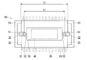
各種電気、電子部品が半田付けされている基板18は、筐体26の所定の部分に固定されている。基板18に搭載される半導体素子21は、半導体チップを収容するパッケージ29を備える。このパッケージ29の側面から突出される複数の端子30が基板18に半田付けされる。なお、パッケージ29の形状は、平面視で長方形の平板状を成す(図6参照)。パッケージ29の4つの側面のうち長手方向の2つの側面に端子30が設けられ、短手方向の2つの側面31には、半導体素子21をネジによってヒートシンク24に固定するための切欠部32が形成されている。
本実施形態では、半導体素子21の下面と基板18の上面との間に固定部材50が設けられる。半導体素子21は、固定部材50を介して、2本のネジ33によりヒートシンク24に取り付けられる。このため、前述の半導体素子21に設けられたネジ止め用の切欠部32は、ネジ止めには使用されない。それぞれのネジ33には、ネジ頭を固定部材50の下面に掛止させるためのワッシャ34が設けられている。なお、固定部材50は、合成樹脂などの可撓性を有する材質で形成された部材である。このようにすれば、固定部材50の製造性を向上させることができる。
ヒートシンク24の基部35の下面は、ネジ33によって固定された半導体素子21の上面に密接に接触する。ヒートシンク24には、筐体26の外部側に突出した複数枚のフィン25が設けられる。このヒートシンク24は、熱伝達率の高いアルミニウムなどの金属で形成された部材である。半導体素子21から発生する熱は、ヒートシンク24により外部に放出され、半導体素子21の温度上昇を防止する。なお、フィン25の形状および寸法は、室外機1を構成する他の構成部材36、例えば室外機1の背面側の筐体2に干渉しない突出寸法になっている。つまり、室外機1の構成に応じてフィン25の形状および突出寸法が設定される。
図5に示すようにヒートシンク24には、特定距離L1を空けて設けられた2つの雌ネジ部37が形成される。これらの雌ネジ部37に前述のネジ33が螺合される。また、雌ネジ部37は、ヒートシンク24の基部35を上下方向に貫通している。なお、ヒートシンク24の雌ネジ部37が外部に貫通していることから、筐体26内に雨水を入り込まないようにするためにネジ33によって確実に封鎖しておく必要がある。
2つの雌ネジ部37は、1つの半導体素子21ごと設けられる。つまり、複数の半導体素子21が設けられる場合には、半導体素子21の数の2倍の雌ネジ部37がヒートシンク24に形成される。
基板18には、ネジ33のネジ頭およびワッシャ34よりも大きい開口寸法を有する2つの大口孔38が貫通されている。これらの大口孔38は、ヒートシンク24の雌ネジ部37のそれぞれに対応する位置に設けられる。
基板18の上面には、半導体素子21の他に、抵抗器などの微小な電子部品39が設けられる。また、基板18の下面には、インバータ装置としての半導体素子21で変換された交流を出力するためのコネクタ40が設けられる。このコネクタ40は、半導体素子21の取付位置に対応して設けられる。コネクタ40には、半導体素子21で変換された交流を基板18の外部に導出するための配線41の端子42が接続される。なお、複数の半導体素子21を基板18上に搭載している場合、そのすべての半導体素子21の位置にコネクタ40が設けられる訳ではなく、コネクタ40が設けられない半導体素子21もある。
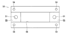
図6から図9に示すように、固定部材50は、平面視で四角形(長方形)の平板状を成す。固定部材50には、特定距離L2を空けて設けられた少なくとも2つのネジ挿通孔51が形成されている。なお、固定部材50の2つのネジ挿通孔51同士の間の特定距離L2は、ヒートシンク24の2つの雌ネジ部37同士の間の特定距離L1と同一距離となっている(図5参照)。つまり、ネジ挿通孔51は、雌ネジ部37に対応する位置に設けられる。ネジ33は、固定部材50の下面側からネジ挿通孔51に挿通され、ヒートシンク24の雌ネジ部37に螺合される。
半導体素子21の切欠部32は、半導体素子21の短手方向の側面31を半円形状に切り欠いた形状をしている。2つの切欠部32同士の離間距離L3は、特定距離L1,L2よりも短い。切欠部32の本来の用途は、切欠部32にネジ33を挿通してヒートシンク24に半導体素子21を固定することである。本来、ヒートシンク24の雌ネジ部37同士の特定距離L1は、切欠部32同士の離間距離L3と一致している。
しかしながら、半導体素子21は年々小型化されるので、新型の半導体素子21の切欠部32同士の離間距離L3は、旧型の半導体素子21の切欠部32同士の離間距離L3よりも小さくなる。つまり、新型の半導体素子21の切欠部32同士の離間距離L3が、ヒートシンク24の雌ネジ部37同士の特定距離L1と一致しなくなる。そして、長年の使用により基板18または旧型の半導体素子21が故障し、室外機1の修理が必要となったときには、既に旧型の半導体素子21の入手が困難になっている場合がある。その場合には、新型の半導体素子21を用いて基板18を新造することになる。
ここで、旧型の半導体素子21に合うヒートシンク24には、新型の半導体素子21の切欠部32に雌ネジ部37の位置が合わず、取り付けできないという問題が生じる。なお、新型の半導体素子21に合わせて基板18を新造することは容易であるが、ヒートシンク24の新造には手間がかかる。特に、ヒートシンク24は、電装箱16の筐体26に固定され、この筐体26は、室外機1の筐体2に固定されており、元のヒートシンク24を取り外して、新たなヒートシンク24を取り付ける場合には、室外機1の数多くの部品を分解、組み立てが必要で手間と時間のかかる作業となる。さらにヒートシンク24と電装箱16の筐体26との間は水密にする必要があり、両者の接合面にコーキング等を施す場合には非常に面倒な作業が発生する。
そこで、本実施形態では、固定部材50を用いることで、旧型の半導体素子21に合わせて製造されたヒートシンク24に、小型の新型の半導体素子21を取り付けるようにしている。このようにすれば、ヒートシンク24を交換せずに新型の半導体素子21が搭載された基板18と交換することができる。なお、固定部材50は、合成樹脂で形成されるので、新型の半導体素子21のサイズの形状に合わせて容易に新造することができる。
図6および図9に示すように、固定部材50は、全体として枠形状で、その上面から上方に突出される2つの上面突起部52を備える。これらの上面突起部52は、平面視で一部に切り欠きを有する円柱形状を成す。それぞれの上面突起部52は、半導体素子21のパッケージ29の切欠部32に係合される。つまり、切欠部32は、係合部としての上面突起部52が係合される被係合部となっている。
このようにすれば、固定部材50の上面突起部52が半導体素子21の切欠部32に係合されるので、半導体素子21の位置決めをすることができる。半導体素子21が横方向(図6の紙面左右方向)および縦方向(図6の紙面上下方向)にぐらつかないようになる。
なお、上面突起部52の円柱形状は、上方に行くに従って窄まる形状を成しても良い。このようにすれば、半導体素子21を上方から固定部材50に載置するときに、切欠部32に上面突起部52を係合させ易くなる。
ネジ挿通孔51にネジ33が挿通されたときに、ネジ33と半導体素子21の切欠部32との間に隙間が設けられる。つまり、ネジ33と半導体素子21の切欠部32とが係合されないようになる。このようにすれば、ネジ33(雌ネジ部37)の位置に影響を受けずに、半導体素子21の位置決めを行うことができる。
固定部材50は、周縁から上方に突出される2つの周縁壁部53を備える。これらの周縁壁部53は、半導体素子21の端子30が設けられていない2つの側面31に対応して設けられる。それぞれの周縁壁部53は、平面視でU字形状を成し、その端部が半導体素子21のパッケージ29の側面31に係合される。つまり、本実施形態の半導体素子21の側面31は、係合部としての周縁壁部53が係合される被係合部となっている。
このようにすれば、固定部材50の周縁壁部53が半導体素子21の側面31に係合されるので、半導体素子21の位置決めをすることができる。半導体素子21が横方向(図6の紙面左右方向)にぐらつかないようになる。周縁壁部53により半導体素子21がぐらつかないように固定することができる。なお、周縁壁部53の突出寸法は、上面突起部52の突出寸法よりも大きくなっている。
図7および図8に示すように、固定部材50は、その下面から下方に突出される4つの下面突起部54を備える。それぞれの下面突起部54は、固定部材50の下面の四隅に設けられる。これらの下面突起部54は、基板18の上面に接触する。このようにすれば、固定部材50の下面と基板18の上面との間に空間が設けられるので、基板18に設けられた微小な電子部品39に固定部材50が干渉しないようになる(図5参照)。
固定部材50の下面には、ネジ33のネジ頭およびワッシャ34が掛止される2つの座金用面55が設けられる。これらの座金用面55は、固定部材50の下面の他の部分よりも高い位置に設けられる。このようにすれば、ネジ33のネジ頭が基板18に設けられた微小な電子部品39に干渉しないようになる。
図6に示すように、固定部材50の中央部には、平面視で四角形(長方形)を成す開口部56が開口されている。この開口部56は、コネクタ40に対応する位置に設けられる。このようにすれば、高電圧が加わるコネクタ40に固定部材50が干渉しないようにできる。また、一般汎用樹脂材を用いて固定部材50を形成できる。すなわち、高電圧部分と距離を話すことができるので、高耐トラッキング材を使用しないで済み、固定部材50を低コストで製造することができる。
図10に示すように、固定部材50をネジ33でヒートシンク24に止める前において、固定部材50の上面から周縁壁部53の上端までの突出寸法T1が、半導体素子21の厚み寸法T2よりも小さくなっている。つまり、周縁壁部53の突出寸法T1と半導体素子21の厚み寸法T2との間に差分D(マイナス誤差)を設けて固定部材50が形成される。このようにすれば、半導体素子21の上面をヒートシンク24の下面に密着させることができる。
図11に示すように、固定部材50をネジ33でヒートシンク24に止めた後において、周縁壁部53の上端がヒートシンク24の下面に接触する。つまり、ネジ33がヒートシンク24の雌ネジ部37に螺合されたときに、その締め付け力により、固定部材50に反りが発生し、周縁壁部53の上端がヒートシンク24の下面に接触する。なお、ネジ33が締め付けられても、周縁壁部53の上端がヒートシンク24の下面に接触されるので、固定部材50に加わる負荷を抑えることができる。
図12に示すように、固定部材50が部品として搬送される場合には、複数個の固定部材50が積み重ねられた状態で梱包される。ここで、固定部材50は、上下に複数の固定部材50が積み重ねられたときに、その下面突起部54が、下段の周縁壁部53の内面側に当接する位置に設けられている。このようにすれば、搬送中に、固定部材50同士が横方向(図12の紙面左右方向)に互いにぐらつかないようになる。
図5に示すように、本実施形態では、固定部材50のネジ挿通孔51がヒートシンク24の雌ネジ部37に対応するので、新型の半導体素子21の形状に関わらず、この半導体素子21をヒートシンク24に固定させることができる。
また、ヒートシンク24の複数箇所に形成された雌ネジ部37は、ネジ33が螺着されることで閉塞される。そのため、これらの雌ネジ部37から水滴が筐体26の内部に浸入しないようになっている。さらに、取り付けられる半導体素子21に応じた数のみの雌ネジ部37がヒートシンク24に形成される。そのため、全ての雌ネジ部37がネジ33により閉塞されるようになる。
また、ヒートシンク24を新造する場合には、フィン25の形状および寸法を他の構成部材36に干渉しないようにしなければならず、その製作に手間がかかる。本実施形態では、ヒートシンク24を電装箱16の取付部27に取り付けたままの状態で、基板18の交換を行うことができるので、ヒートシンク24を新造しなくても済む。つまり、古いヒートシンク24を流用することができる。
また、固定部材50は、基板18に固定されないので、固定部材50の寸法管理を厳密に行う必要がない。そのため、固定部材50の製造性を向上させることができる。
次に、制御装置17の保守方法について図13のフローチャート(手順図)を用いて説明する。なお、図4から11を適宜参照する。なお、図13中のステップS11~S13が基板18の製造方法で、S14以降が制御装置17の交換方法となっており、これらを合わせて制御装置17の保守方法として説明する。
まず、ステップS11において、製造者は、保守用の新しい基板18を製造するときに、固定部材50を新しい基板18に仮固定として取り付ける。例えば、新しい基板18の下方側から所定の治具のピンを大口孔38に挿入し、この治具のピンを固定部材50のネジ挿通孔51に挿通させる。このようにすれば、治具のピンにより固定部材50が位置決めされる。
次のステップS12において、製造者は、固定部材50の上面に新型の半導体素子21を載置する。ここで、固定部材50の係合部としての上面突起部52を半導体素子21の被係合部としての切欠部32に係合する。さらに、固定部材50の係合部としての周縁壁部53を半導体素子21の被係合部としての側面31に係合する。
次のステップS13において、製造者は、半導体素子21を新しい基板18に搭載する。つまり、半導体素子21の端子30を基板18に半田付けする。この半田付けの後に、所定の治具を新しい基板18から取り外す。
次のステップS14において、作業者は、室外機1のメンテナンス作業を開始する。ここで、作業者は、電装箱16から古い基板18を取り外す。古い基板18には、固定部材50が設けられておらず、半導体素子21は、切欠部32を介してヒートシンク24に直接ネジ止めされている。そこで、まず、半導体素子21を固定しているネジ33を取り外す。その後、古い基板18を取り外す。なお、ヒートシンク24は電装箱16に取り付けられた状態のまま維持される。
次のステップS15において、作業者は、保守用の新しい基板18を電装箱16の内部に収容する。つまり、新しい基板18を電装箱16に取り付ける。
次のステップS16において、作業者は、新しい基板18を電装箱16に取り付けることで、ヒートシンク24の下面に半導体素子21の上面を接触させる。
次のステップS17において、作業者は、新しい基板18の下方側から大口孔38を介してネジ33を挿入する。そして、ネジ33を固定部材50のネジ挿通孔51に挿通する。
次のステップS18において、作業者は、ネジ挿通孔51に挿通されたネジ33をヒートシンク24の雌ネジ部37に螺合する。そして、室外機1のメンテナンス作業を終了する。
なお、本実施形態のフローチャートにおいて、各ステップが直列に実行される形態を例示しているが、必ずしも各ステップの前後関係が固定されるものでなく、一部のステップの前後関係が入れ替わっても良い。また、一部のステップが他のステップと並列に実行されても良い。
なお、本実施形態では、ヒートシンク24に2つの雌ネジ部37が形成され、固定部材50に2つのネジ挿通孔51が形成されているが、その他の態様であっても良い。例えば、ヒートシンク24に2つの雌ネジ部37がある場合に、固定部材50に形成されるネジ挿通孔51が1つであっても良い。そして、固定部材50の1つのネジ挿通孔51にネジ33を挿通して半導体素子21の一端を固定し、半導体素子21の他端の切欠部32にネジ33を挿通してこの他端を固定しても良い。つまり、固定部材50には、少なくとも1つのネジ挿通孔51が半導体素子21の切欠部32から離れて設けられていれば良い。
また、半導体素子21によっては、側面31の切欠部32の代わりに長手方向の両端部にネジ止め用の穴を設けている場合もある。この場合は、ネジ止め用の穴を被係合部として用いればよい。なお、半導体素子21の両端部のネジ止め用の穴を被係合部として用いる場合は、これらの穴はネジ止めに使用されない。
以上説明した実施形態によれば、半導体素子の下面と基板との間に設けられる固定部材を備えることにより、ヒートシンクを交換することなく異なる半導体素子を搭載した基板を取り付けることができる。さらに、本実施形態によれば、補修部品に限らず、製造段階において、同じヒートシンクに異なる寸法の半導体素子を搭載した基板を併用することも可能となる。
本発明のいくつかの実施形態を説明したが、これらの実施形態は、例として提示したものであり、発明の範囲を限定することは意図していない。これら実施形態は、その他の様々な形態で実施されることが可能であり、発明の要旨を逸脱しない範囲で、種々の省略、置き換え、変更、組み合わせを行うことができる。これら実施形態やその変形は、発明の範囲や要旨に含まれると同様に、特許請求の範囲に記載された発明とその均等の範囲に含まれるものである。
1…室外機、2…筐体、3…開口部、16…電装箱、17…制御装置、18…基板(プリント回路基板)、21(21A~21F)…半導体素子、23…制御部、24…ヒートシンク、25…フィン、26…電装箱の筐体、27…取付部、28…保持片、29…パッケージ、30…端子、31…側面(被係合部)、32…切欠部(被係合部)、33…ネジ、37…雌ネジ部、40…コネクタ、50…固定部材、51…ネジ挿通孔、52…上面突起部、53…周縁壁部、54…下面突起部、55…座金用面、56…開口部、D…差分、L1,L2…特定距離、L3…離間距離、T1…突出寸法、T2…厚み寸法。
Claims (11)
- 半導体素子と、
前記半導体素子が搭載される基板と、
前記半導体素子の上面に接触されるヒートシンクと、
前記ヒートシンクに形成された雌ネジ部と、
前記半導体素子の下面と前記基板との間に設けられる固定部材と、
前記固定部材の前記雌ネジ部に対応する位置に形成されたネジ挿通孔と、
前記固定部材に形成され、前記半導体素子の被係合部に係合される係合部と、
前記ネジ挿通孔に挿通され、前記雌ネジ部に螺合されるネジと、
を備える制御装置。 - 少なくとも2つの前記雌ネジ部が特定距離を空けて前記ヒートシンクに設けられ、かつ少なくとも2つの前記ネジ挿通孔が前記特定距離を空けて前記固定部材に設けられる請求項1に記載の制御装置。
- 前記被係合部が前記半導体素子に形成されたネジ止め用の切欠部または穴であり、前記係合部が前記固定部材の上面から上方に突出される上面突起部である請求項1に記載の制御装置。
- 前記被係合部が前記半導体素子の側面であり、前記係合部が前記固定部材の周縁から上方に突出される周縁壁部である請求項1に記載の制御装置。
- 前記固定部材の上面から前記周縁壁部の上端までの寸法が、前記半導体素子の厚み寸法よりも小さい請求項4に記載の制御装置。
- 前記固定部材が可撓性を有する材質で形成され、前記ネジが前記雌ネジ部に螺合されたときに、前記周縁壁部の上端が前記ヒートシンクの下面に接触される請求項4に記載の制御装置。
- 前記固定部材の下面から下方に突出される下面突起部を備える請求項1に記載の制御装置。
- 前記固定部材の周縁から上方に突出され、前記半導体素子の被係合部に係合される周縁壁部と、
前記固定部材の下面から下方に突出される下面突起部と、
を備え、
少なくとも2つの前記固定部材が積み重ねられたときに、前記下面突起部が前記周縁壁部の内面側に接触される請求項1に記載の制御装置。 - 直流を交流に変換するインバータとしての前記半導体素子で変換された交流を前記基板の外部に導出する配線が接続されるコネクタと、
前記固定部材の前記コネクタに対応する位置に開口された開口部と、
を備える請求項1に記載の制御装置。 - 前記基板を収容する電装箱と、
前記電装箱に形成され、前記ヒートシンクが取り付けられる取付部と、
を備える請求項1に記載の制御装置。 - 半導体素子の下面と基板との間に固定部材を設けるステップと、
前記固定部材に形成された係合部を前記半導体素子の被係合部に係合するステップと、
前記半導体素子を前記基板に搭載するステップと、
雌ネジ部が形成されたヒートシンクに前記半導体素子の上面を接触させるステップと、
前記固定部材の前記雌ネジ部に対応する位置に形成されたネジ挿通孔にネジを挿通するステップと、
前記ネジを前記雌ネジ部に螺合するステップと、
を含む制御装置の保守方法。
Priority Applications (3)
| Application Number | Priority Date | Filing Date | Title |
|---|---|---|---|
| JP2020547491A JP7072076B2 (ja) | 2018-09-18 | 2018-09-18 | 制御装置および制御装置の保守方法 |
| PCT/JP2018/034415 WO2020059010A1 (ja) | 2018-09-18 | 2018-09-18 | 制御装置および制御装置の保守方法 |
| CN201880097239.1A CN112655086B (zh) | 2018-09-18 | 2018-09-18 | 控制装置以及控制装置的保养方法 |
Applications Claiming Priority (1)
| Application Number | Priority Date | Filing Date | Title |
|---|---|---|---|
| PCT/JP2018/034415 WO2020059010A1 (ja) | 2018-09-18 | 2018-09-18 | 制御装置および制御装置の保守方法 |
Publications (1)
| Publication Number | Publication Date |
|---|---|
| WO2020059010A1 true WO2020059010A1 (ja) | 2020-03-26 |
Family
ID=69886934
Family Applications (1)
| Application Number | Title | Priority Date | Filing Date |
|---|---|---|---|
| PCT/JP2018/034415 Ceased WO2020059010A1 (ja) | 2018-09-18 | 2018-09-18 | 制御装置および制御装置の保守方法 |
Country Status (3)
| Country | Link |
|---|---|
| JP (1) | JP7072076B2 (ja) |
| CN (1) | CN112655086B (ja) |
| WO (1) | WO2020059010A1 (ja) |
Cited By (1)
| Publication number | Priority date | Publication date | Assignee | Title |
|---|---|---|---|---|
| JP7438434B1 (ja) | 2023-06-27 | 2024-02-26 | 日立ジョンソンコントロールズ空調株式会社 | 空気調和機用回路構造体及び空気調和機 |
Citations (7)
| Publication number | Priority date | Publication date | Assignee | Title |
|---|---|---|---|---|
| JPH0479440U (ja) * | 1990-11-22 | 1992-07-10 | ||
| JP2002076221A (ja) * | 2000-08-29 | 2002-03-15 | Kenwood Corp | 電子部品と放熱器との組付け構造 |
| JP2008004869A (ja) * | 2006-06-26 | 2008-01-10 | Daikin Ind Ltd | 電気部品 |
| JP2009026871A (ja) * | 2007-07-18 | 2009-02-05 | Denso Corp | 電子装置の製造方法 |
| JP2013089784A (ja) * | 2011-10-19 | 2013-05-13 | Hitachi Ltd | 半導体装置 |
| WO2016162991A1 (ja) * | 2015-04-08 | 2016-10-13 | 三菱電機株式会社 | 半導体装置および半導体装置の製造方法 |
| WO2017138341A1 (ja) * | 2016-02-12 | 2017-08-17 | 東芝キヤリア株式会社 | 放熱装置および放熱装置の組み立て方法 |
Family Cites Families (2)
| Publication number | Priority date | Publication date | Assignee | Title |
|---|---|---|---|---|
| ITPD20020048A1 (it) * | 2002-02-26 | 2003-08-26 | Fischer Italia Srl Unipersonal | Dispositivo di fissaggio a scomparsa per oggettistica di tipo sospeso. |
| WO2006001163A1 (ja) * | 2004-06-24 | 2006-01-05 | Kabushiki Kaisha Yaskawa Denki | モータ制御装置 |
-
2018
- 2018-09-18 CN CN201880097239.1A patent/CN112655086B/zh active Active
- 2018-09-18 JP JP2020547491A patent/JP7072076B2/ja active Active
- 2018-09-18 WO PCT/JP2018/034415 patent/WO2020059010A1/ja not_active Ceased
Patent Citations (7)
| Publication number | Priority date | Publication date | Assignee | Title |
|---|---|---|---|---|
| JPH0479440U (ja) * | 1990-11-22 | 1992-07-10 | ||
| JP2002076221A (ja) * | 2000-08-29 | 2002-03-15 | Kenwood Corp | 電子部品と放熱器との組付け構造 |
| JP2008004869A (ja) * | 2006-06-26 | 2008-01-10 | Daikin Ind Ltd | 電気部品 |
| JP2009026871A (ja) * | 2007-07-18 | 2009-02-05 | Denso Corp | 電子装置の製造方法 |
| JP2013089784A (ja) * | 2011-10-19 | 2013-05-13 | Hitachi Ltd | 半導体装置 |
| WO2016162991A1 (ja) * | 2015-04-08 | 2016-10-13 | 三菱電機株式会社 | 半導体装置および半導体装置の製造方法 |
| WO2017138341A1 (ja) * | 2016-02-12 | 2017-08-17 | 東芝キヤリア株式会社 | 放熱装置および放熱装置の組み立て方法 |
Cited By (2)
| Publication number | Priority date | Publication date | Assignee | Title |
|---|---|---|---|---|
| JP7438434B1 (ja) | 2023-06-27 | 2024-02-26 | 日立ジョンソンコントロールズ空調株式会社 | 空気調和機用回路構造体及び空気調和機 |
| JP2025004788A (ja) * | 2023-06-27 | 2025-01-16 | 日立ジョンソンコントロールズ空調株式会社 | 空気調和機用回路構造体及び空気調和機 |
Also Published As
| Publication number | Publication date |
|---|---|
| CN112655086A (zh) | 2021-04-13 |
| CN112655086B (zh) | 2023-12-26 |
| JPWO2020059010A1 (ja) | 2021-08-30 |
| JP7072076B2 (ja) | 2022-05-19 |
Similar Documents
| Publication | Publication Date | Title |
|---|---|---|
| US20160223183A1 (en) | Led lamp | |
| TW200843620A (en) | Motor control device | |
| US20180010836A1 (en) | Heat transfer unit | |
| JP4093479B2 (ja) | 電源装置 | |
| WO2017115431A1 (ja) | 回路基板、アクティブフィルタ装置、及び空気調和機 | |
| JP7028959B2 (ja) | 制御装置の製造方法および制御装置 | |
| JP7072076B2 (ja) | 制御装置および制御装置の保守方法 | |
| US9351420B2 (en) | Systems and methods for manufacturing industrial automation drives | |
| JP6435717B2 (ja) | 冷凍装置 | |
| JP2012200071A (ja) | モータ制御装置 | |
| US12218612B2 (en) | Inverter unit | |
| CN111670325B (zh) | 电气装置模块 | |
| US12261546B2 (en) | Inverter unit | |
| CN106937492A (zh) | 电器盒及具有其的空调器 | |
| JP7081336B2 (ja) | 電装品モジュール | |
| US12213290B2 (en) | Electrical device and method for producing a first and second electrical device from a kit | |
| JP2013252006A (ja) | モータ駆動装置及びそれを備えた空気調和機 | |
| JP6121290B2 (ja) | 冷凍装置 | |
| JP2007250700A (ja) | 半導体装置 | |
| JP2005114339A (ja) | 空気調和機の室外機 | |
| JP2016050725A (ja) | 冷凍装置 | |
| CN111656099B (zh) | 电气装置模块 | |
| KR20090007285U (ko) | 공기조화기의 실외기 | |
| JP2023041377A (ja) | パワー基板およびそれを用いた空気調和機の室外機 | |
| KR100557766B1 (ko) | 공기조화기 |
Legal Events
| Date | Code | Title | Description |
|---|---|---|---|
| 121 | Ep: the epo has been informed by wipo that ep was designated in this application |
Ref document number: 18934040 Country of ref document: EP Kind code of ref document: A1 |
|
| ENP | Entry into the national phase |
Ref document number: 2020547491 Country of ref document: JP Kind code of ref document: A |
|
| NENP | Non-entry into the national phase |
Ref country code: DE |
|
| 122 | Ep: pct application non-entry in european phase |
Ref document number: 18934040 Country of ref document: EP Kind code of ref document: A1 |