WO2020049953A1 - 撮像素子および撮像素子の製造方法 - Google Patents
撮像素子および撮像素子の製造方法 Download PDFInfo
- Publication number
- WO2020049953A1 WO2020049953A1 PCT/JP2019/031553 JP2019031553W WO2020049953A1 WO 2020049953 A1 WO2020049953 A1 WO 2020049953A1 JP 2019031553 W JP2019031553 W JP 2019031553W WO 2020049953 A1 WO2020049953 A1 WO 2020049953A1
- Authority
- WO
- WIPO (PCT)
- Prior art keywords
- curved
- holding
- bending
- imaging device
- image sensor
- Prior art date
- Legal status (The legal status is an assumption and is not a legal conclusion. Google has not performed a legal analysis and makes no representation as to the accuracy of the status listed.)
- Ceased
Links
Images






Classifications
-
- H—ELECTRICITY
- H10—SEMICONDUCTOR DEVICES; ELECTRIC SOLID-STATE DEVICES NOT OTHERWISE PROVIDED FOR
- H10F—INORGANIC SEMICONDUCTOR DEVICES SENSITIVE TO INFRARED RADIATION, LIGHT, ELECTROMAGNETIC RADIATION OF SHORTER WAVELENGTH OR CORPUSCULAR RADIATION
- H10F39/00—Integrated devices, or assemblies of multiple devices, comprising at least one element covered by group H10F30/00, e.g. radiation detectors comprising photodiode arrays
- H10F39/80—Constructional details of image sensors
-
- H—ELECTRICITY
- H04—ELECTRIC COMMUNICATION TECHNIQUE
- H04N—PICTORIAL COMMUNICATION, e.g. TELEVISION
- H04N25/00—Circuitry of solid-state image sensors [SSIS]; Control thereof
- H04N25/70—SSIS architectures; Circuits associated therewith
-
- H—ELECTRICITY
- H10—SEMICONDUCTOR DEVICES; ELECTRIC SOLID-STATE DEVICES NOT OTHERWISE PROVIDED FOR
- H10F—INORGANIC SEMICONDUCTOR DEVICES SENSITIVE TO INFRARED RADIATION, LIGHT, ELECTROMAGNETIC RADIATION OF SHORTER WAVELENGTH OR CORPUSCULAR RADIATION
- H10F39/00—Integrated devices, or assemblies of multiple devices, comprising at least one element covered by group H10F30/00, e.g. radiation detectors comprising photodiode arrays
- H10F39/011—Manufacture or treatment of image sensors covered by group H10F39/12
- H10F39/024—Manufacture or treatment of image sensors covered by group H10F39/12 of coatings or optical elements
-
- H—ELECTRICITY
- H10—SEMICONDUCTOR DEVICES; ELECTRIC SOLID-STATE DEVICES NOT OTHERWISE PROVIDED FOR
- H10F—INORGANIC SEMICONDUCTOR DEVICES SENSITIVE TO INFRARED RADIATION, LIGHT, ELECTROMAGNETIC RADIATION OF SHORTER WAVELENGTH OR CORPUSCULAR RADIATION
- H10F39/00—Integrated devices, or assemblies of multiple devices, comprising at least one element covered by group H10F30/00, e.g. radiation detectors comprising photodiode arrays
- H10F39/011—Manufacture or treatment of image sensors covered by group H10F39/12
- H10F39/026—Wafer-level processing
-
- H—ELECTRICITY
- H10—SEMICONDUCTOR DEVICES; ELECTRIC SOLID-STATE DEVICES NOT OTHERWISE PROVIDED FOR
- H10F—INORGANIC SEMICONDUCTOR DEVICES SENSITIVE TO INFRARED RADIATION, LIGHT, ELECTROMAGNETIC RADIATION OF SHORTER WAVELENGTH OR CORPUSCULAR RADIATION
- H10F39/00—Integrated devices, or assemblies of multiple devices, comprising at least one element covered by group H10F30/00, e.g. radiation detectors comprising photodiode arrays
- H10F39/80—Constructional details of image sensors
- H10F39/804—Containers or encapsulations
-
- H—ELECTRICITY
- H10—SEMICONDUCTOR DEVICES; ELECTRIC SOLID-STATE DEVICES NOT OTHERWISE PROVIDED FOR
- H10F—INORGANIC SEMICONDUCTOR DEVICES SENSITIVE TO INFRARED RADIATION, LIGHT, ELECTROMAGNETIC RADIATION OF SHORTER WAVELENGTH OR CORPUSCULAR RADIATION
- H10F39/00—Integrated devices, or assemblies of multiple devices, comprising at least one element covered by group H10F30/00, e.g. radiation detectors comprising photodiode arrays
- H10F39/80—Constructional details of image sensors
- H10F39/806—Optical elements or arrangements associated with the image sensors
- H10F39/8063—Microlenses
Definitions
- the present disclosure relates to an imaging device and a method for manufacturing the imaging device. More specifically, the present invention relates to an imaging device having a curved light receiving surface and a method for manufacturing the imaging device.
- a solid-state imaging device containing a solid-state imaging device that captures an image of a subject formed by a photographing lens has been used.
- There is an aberration in a taking lens and there is a problem in that, when an image of a subject is formed on a solid-state imaging device having a planar shape, blurring occurs at a center portion or an end of the solid-state imaging device. Therefore, an imaging apparatus has been proposed in which the solid-state imaging device is curved in accordance with the aberration of the photographing lens, thereby preventing the occurrence of blur at the center and at the end.
- a flat semiconductor substrate having a first surface on which a solid-state imaging device is formed and a second surface which is a back surface of the first surface, and a planar third surface and a back surface of the third surface
- a solid-state imaging device including a resin layer having a fourth surface on which a curved concave portion is formed.
- the fourth surface of the resin layer is bonded to the package after the second surface of the semiconductor substrate and the third surface of the resin layer are bonded.
- the resin layer is deformed according to the shape of the concave portion on the fourth surface by being closely attached to the package and adhered to the first surface and the second surface of the solid-state imaging device.
- a concave portion can be formed (for example, see Patent Document 1).
- the present disclosure has been made in view of the above-described problems, and has as its object to simplify a method of manufacturing an imaging device having a light receiving surface that is curved in accordance with the aberration of an imaging lens.
- a first aspect of the present disclosure is a semiconductor chip having a concave portion formed on a back surface that is different from a light receiving surface that receives light from a subject.
- An imaging chip configured by: a bending forming unit that is disposed in the concave portion and forms the bending portion by bending the imaging chip at the bottom of the concave portion; and a bending holding unit that holds the formed bending portion. It is an imaging device provided.
- the bending portion may be configured to have a higher linear expansion coefficient than the imaging chip and be heated to form the bending portion.
- the curved portion may be made of metal.
- the curved holding section may be made of a thermosetting resin.
- the bending portion may form the bending portion when the bending holding portion hardens.
- the curved holding portion may be made of a thermosetting resin that contracts during curing.
- a lid may be further provided, which is disposed adjacent to the bending holding portion and limits shrinkage of the bending holding portion near the opening of the concave portion.
- the curved holding portion may be configured by a holding base in which a second concave portion that fits into the bent portion is arranged, and an adhesive portion that is arranged between the holding base and the curved forming portion.
- the semiconductor chip may further include an etching prevention layer disposed at the bottom of the concave portion of the semiconductor chip to prevent etching of the semiconductor chip.
- a second aspect of the present disclosure includes a concave portion forming step of forming a concave portion on a back surface that is different from a light receiving surface for receiving light from a subject in an imaging chip formed on a semiconductor chip, and a bottom portion of the concave portion.
- a holding step is
- the curved forming portion and the curved holding portion are arranged near the bottom of the concave portion formed on the back surface of the imaging chip, and have an effect of holding the imaging chip in a state curved in the back surface direction. It is assumed that the formation of the curved portion on the light receiving surface of the imaging chip is simplified.
- an excellent effect of simplifying a method of manufacturing an imaging device having a light receiving surface curved according to the aberration of a photographic lens is achieved.
- FIG. 1 is a block diagram illustrating a configuration example of an imaging device according to an embodiment of the present disclosure.
- 1 is a diagram illustrating a configuration example of an imaging element according to an embodiment of the present disclosure.
- FIG. 1 is a cross-sectional view illustrating a configuration example of an imaging device according to a first embodiment of the present disclosure.
- FIG. 4 is a cross-sectional view illustrating another configuration example of the imaging element according to the first embodiment of the present disclosure.
- FIG. 1 is a cross-sectional view illustrating a configuration example of an imaging device according to a first embodiment of the present disclosure.
- FIG. 2 is a diagram illustrating an example of a curve according to the first embodiment of the present disclosure.
- FIG. 2 is a diagram illustrating an example of a method for manufacturing an imaging device according to the first embodiment of the present disclosure.
- FIG. 2 is a diagram illustrating an example of a method for manufacturing an imaging device according to the first embodiment of the present disclosure.
- FIG. 10 is a cross-sectional view illustrating a configuration example of an imaging device according to a second embodiment of the present disclosure.
- FIG. 13 is a cross-sectional view illustrating a configuration example of an imaging element according to a third embodiment of the present disclosure.
- FIG. 14 is a cross-sectional view illustrating a configuration example of an imaging device according to a fourth embodiment of the present disclosure.
- FIG. 14 is a cross-sectional view illustrating another configuration example of the imaging element according to the fourth embodiment of the present disclosure.
- FIG. 10 is a cross-sectional view illustrating a configuration example of an imaging device according to a second embodiment of the present disclosure.
- FIG. 13 is a cross-sectional view illustrating a configuration example of an imaging element according
- FIG. 15 is a cross-sectional view illustrating a configuration example of an imaging device according to a fifth embodiment of the present disclosure.
- FIG. 16 is a cross-sectional view illustrating a configuration example of an imaging device according to a sixth embodiment of the present disclosure.
- FIG. 16 is a cross-sectional view illustrating a configuration example of an imaging device according to a seventh embodiment of the present disclosure.
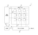
- FIG. 1 is a block diagram illustrating a configuration example of an imaging device according to an embodiment of the present disclosure. 1 includes a pixel array unit 10, a vertical drive unit 20, a column signal processing unit 30, and a control unit 40.
- the pixel array section 10 is configured by arranging the pixels 100 in a two-dimensional lattice.
- the pixel 100 generates an image signal corresponding to the emitted light.
- the pixel 100 has a photoelectric conversion unit that generates a charge according to the irradiated light.
- the pixel 100 further includes a pixel circuit. This pixel circuit generates an image signal based on the electric charge generated by the photoelectric conversion unit. The generation of the image signal is controlled by a control signal generated by a vertical drive unit 20 described later.
- signal lines 11 and 12 are arranged in an XY matrix.
- the signal line 11 is a signal line for transmitting a control signal of a pixel circuit in the pixel 100, is arranged for each row of the pixel array section 10, and is commonly wired to the pixels 100 arranged in each row.
- the signal line 12 is a signal line that transmits an image signal generated by the pixel circuit of the pixel 100, is arranged for each column of the pixel array unit 10, and is wired in common to the pixels 100 arranged in each column. You. These photoelectric conversion units and pixel circuits are formed in a semiconductor substrate 111 and a wiring region 121 described later.
- the vertical drive unit 20 generates a control signal for the pixel circuit of the pixel 100.
- the vertical drive unit 20 transmits the generated control signal to the pixel 100 via the signal line 11 in FIG.
- the column signal processing unit 30 processes an image signal generated by the pixel 100.
- the column signal processing unit 30 processes an image signal transmitted from the pixel 100 via the signal line 12 in FIG.
- the processing in the column signal processing unit 30 corresponds to, for example, analog-to-digital conversion for converting an analog image signal generated in the pixel 100 into a digital image signal.
- the image signal processed by the column signal processing unit 30 is output as an image signal of the image sensor 1.
- the control unit 40 controls the entire image sensor 1.
- the control unit 40 controls the image sensor 1 by generating and outputting a control signal for controlling the vertical drive unit 20 and the column signal processing unit 30.
- the control signal generated by the control unit 40 is transmitted to the vertical drive unit 20 and the column signal processing unit 30 via signal lines 41 and 42, respectively.
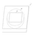
- FIG. 2 is a diagram illustrating a configuration example of the imaging element according to the embodiment of the present disclosure.
- FIG. 1 is an external view illustrating a configuration example of the image sensor 1.
- the pixel array unit 10 described in FIG. 1 is formed on a light receiving surface that receives light from a subject.
- a cylindrical concave portion 149 is formed on the back surface different from the light receiving surface.
- the bottom surface of the concave portion 149 is curved in the direction of the back surface in the same figure, and the pixel array section 10 is also configured to be curved in accordance with this curvature. As a result, it is possible to prevent a decrease in image quality due to aberration of the photographing lens.
- the shape of the recess 149 is not limited to this example.
- the shape may be a square pillar or an octagonal pillar.
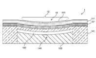
- FIG. 3 is a cross-sectional view illustrating a configuration example of the imaging element according to the first embodiment of the present disclosure.
- the image sensor 1 shown in the figure includes a semiconductor substrate 111, a wiring region 121, a bending forming section 160, and a bending holding section 150.
- the semiconductor substrate 111 is a semiconductor substrate on which the semiconductor element portion of the pixel array section 10 is formed.
- the semiconductor substrate 111 can be made of, for example, silicon.
- the photoelectric conversion unit, the pixel circuit, the vertical drive unit 20, and the like described in FIG. 1 are formed on the semiconductor substrate 111.
- a wiring region 121 is formed on the surface of the semiconductor substrate 111, and a color filter and an on-chip lens (not shown) are arranged on the surface of the wiring region 121.
- the color filter is an optical filter that transmits light of a predetermined wavelength of the incident light
- the on-chip lens is a lens that is disposed for each pixel 100 and collects the incident light.
- the image sensor 1 in FIG. 1 corresponds to a surface-illuminated image sensor in which incident light is applied to the pixels 100 from the front side of the semiconductor substrate 111.
- the recess 149 can be formed, for example, by etching the semiconductor substrate 111.
- the wiring region 121 is a region where a wiring for transmitting a signal is formed.
- This wiring region is composed of a wiring layer on which wiring is formed and an insulating layer for insulating the wiring.
- the signal lines 11, 12, 41 and 42 described in FIG. 1 are arranged in the wiring area 121.
- the wiring layer can be made of, for example, a metal such as copper (Cu) or aluminum (Al).
- the insulating layer can be made of, for example, silicon oxide (SiO 2 ).
- the semiconductor substrate 111 and the wiring region 121 are provided with a curved portion 19 that is curved in the back surface direction. Note that the semiconductor substrate 111 and the wiring region 121 constitute an imaging chip.
- the curving portion 160 is disposed in the concave portion 149, and forms the curving portion 19 by curving the semiconductor substrate 111 and the wiring region 121.
- the curved portion 160 can be made of a material having a higher coefficient of linear expansion than the semiconductor substrate 111 and the wiring region 121.
- a metal may be used for the curved portion 160. It can.
- Cu, Al, gold (Au), platinum (Pt), titanium (Ti), nickel (Ni), and tantalum (Ta) can be used as the curved portion 160.
- the semiconductor substrate 111, the wiring region 121, and the curved portion 160 are heated to expand.
- the coefficient of linear expansion of the curve forming portion 160 is higher than that of the semiconductor substrate 111 and the wiring region 121, the semiconductor substrate 111 and the wiring region 121 can be curved in the back direction as shown in FIG. Further, by arranging the curved forming portion 160, the strength of the imaging chip in which the concave portion 149 is formed can be improved.
- the bending holding section 150 holds the bending section 19.
- the curved holding section 150 is arranged in the concave portion 149 in which the curved section 19 is formed, and can be made of, for example, a resin. By bonding the bending holding section 150 to the semiconductor substrate 111 and the wiring region 121, the bending section 19 can be held while maintaining the bending state.
- a light-curing resin or a thermosetting resin can be used for the curved holding section 150.
- the curved holding section 150 be made of a thermosetting resin. This is because the bending portion 19 can be formed by the bending portion 160 by heating when the bending holding portion 150 is cured.
- the liquid-state curved holding unit 150 is disposed in the concave portion 149, and the imaging chip, the curved forming unit 160, and the curved holding unit 150 are heated to the curing temperature of the curved holding unit 150. Due to this heating, the curved portion 160 expands to form the curved portion 19. After that, the curved holding section 150 is cured. Since the bending holding section 150 is hardened, the bending section 19 can be held even when the temperature of the imaging chip is returned to room temperature. In addition, the above-mentioned bending part 160 can form the bending part 19 when at least a part of the bending holding part 150 is cured.
- a resin that shrinks during curing can be used as the curved holding section 150.
- the bending portion 19 can be formed by contraction of the bending holding portion 150 in addition to the bending forming portion 160.
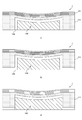
- FIG. 4 is a cross-sectional view illustrating another configuration example of the imaging element according to the first embodiment of the present disclosure.
- “A” in the same figure represents an example in which the curved forming portion 160 is arranged on the bottom surface and the side surface of the concave portion 149.
- “B” in the same figure represents an example in which the curved portion 160 is arranged on the bottom and side surfaces of the concave portion 149 and on the back surface of the semiconductor substrate 111.
- c represents an example in which the curved forming portion 160 is arranged on the bottom surface of the concave portion 149 and the back surface of the semiconductor substrate 111.
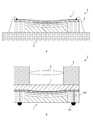
- FIG. 5 is a cross-sectional view illustrating a configuration example of the imaging device according to the first embodiment of the present disclosure.
- “A” in FIG. 2 shows an example in which the image sensor 1 is mounted on the circuit board 4.
- the image sensor 1 is die-bonded to a circuit board 4, and the image sensor 1 and the circuit board 4 are electrically connected by bonding wires 3.
- Pads (not shown) to which the bonding wires 3 are connected are arranged on the image sensor 1.
- This pad is arranged on the periphery of the image sensor 1. Since this area is an area outside the curved portion 19, it is an area parallel to the mounting surface of the circuit board 4. Therefore, wire bonding can be performed without being affected by the curved portion 19.
- ⁇ Circle over (b) ⁇ in the figure represents an example of an imaging module in which the photographing lens 6 and the actuator 5 are arranged and configured in a CSP (Chip Size Package).
- the actuator 5 drives the photographing lens 6.
- This actuator 5 is arranged on the image sensor 1 via the protective glass 7. Since the curved portion 19 is arranged on the light receiving surface of the image sensor 1, the spacer can be omitted, and the protective glass 7 and the image sensor 1 can be directly bonded with an adhesive or the like. Note that a spacer can be disposed between the protective glass 7 and the image sensor 1.
- a solder bump 129 is arranged on the back surface of the image sensor 1. The wiring region 121 and the solder bump 129 are connected by a via 128.
- FIG. 6 is a diagram illustrating an example of a curve according to the first embodiment of the present disclosure.
- FIG. 7 is a diagram illustrating the relationship between the thickness of the bending section 160 and the amount of bending.
- the amount of bending indicates the maximum value of the amount of warpage of the bending portion 19 with respect to the surface of the imaging device 1 on the light receiving surface.
- a solid line graph 301 and a dotted line graph 302 in the same drawing are graphs showing the relationship between the thickness of the bending portion 160 and the amount of bending at heating temperatures of 160 ° C. and 200 ° C., respectively.
- the amount of bending can be changed by changing the thickness of the bending portion.
- the amount of bending has a maximum value. Therefore, the curing temperature and the like can be adjusted so that the desired amount of curvature is close to the local maximum value in the graph, and the configuration can be made less susceptible to errors in the thickness of the curve forming section 160.
- FIG. 7 and 8 are diagrams illustrating an example of a method for manufacturing the imaging device according to the first embodiment of the present disclosure. 7 and 8 are views illustrating an example of a manufacturing process of the imaging device 1. FIG.
- a semiconductor element such as a photoelectric conversion unit or a pixel circuit is formed on the semiconductor substrate 111, and a wiring region 121 is formed (a in FIG. 7).
- a color filter (not shown) and the on-chip lens 101 are arranged on the surface of the wiring area 121 (b in FIG. 7).
- a concave portion 149 is formed on the back surface of the semiconductor substrate 111 (c in FIG. 7).
- This can be done by etching.
- the etching can be performed by forming a mask of a resist or the like having an opening at a position where the concave portion 149 is to be formed on the back surface of the semiconductor substrate 111 and spraying an aqueous solution of potassium hydroxide or the like for etching.
- the etching of the semiconductor substrate 111 can be performed by dry etching. This step is an example of the recess forming step described in the claims.
- the curved portion 160 is arranged in the concave portion 149 (d in FIG. 8). This can be done, for example, by sputtering or plating.
- the curved holding unit 150 is arranged in the concave portion 149 (e in FIG. 8). This can be performed, for example, by applying a liquid resin as a material of the curved holding section 150 to the concave portion 149 by a dispenser or the like. It should be noted that the liquid resin is applied by inverting the top and bottom of the image sensor 1 in FIG. 8 to hold the applied liquid resin.
- the image sensor chip is heated. Thereby, the curved portion 19 is formed by the curved portion 160.
- This step is an example of the curved part forming step described in the claims.
- the curved holding section 150 is cured, and the formed curved section 19 is held (f in FIG. 8).
- This step is an example of the bending portion holding step described in the claims.
- the bending portion 160 having a higher linear expansion coefficient than the imaging device chip is arranged in the concave portion 149 of the semiconductor chip, and the bending portion 160 is heated. 19 is formed. After that, the bending section 19 formed by the bending holding section 150 is held. Thereby, the manufacturing process of the imaging element 1 having the curved portion 19 can be simplified.
- the image sensor 1 according to the first embodiment described above is configured by a surface-illuminated image sensor.
- the image sensor 1 according to the second embodiment of the present disclosure is different from the above-described first embodiment in that the image sensor 1 is configured by a back-illuminated image sensor.
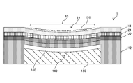
- FIG. 9 is a cross-sectional view illustrating a configuration example of an imaging element according to the second embodiment of the present disclosure.
- the imaging device 1 of FIG. 3 differs from the imaging device 1 described in FIG. 3 in that the imaging device 1 having a configuration in which the semiconductor substrate 111 and the wiring region 121 are interchanged is used. That is, in the imaging device 1 shown in FIG. 1, the wiring region 121 is arranged on the front surface (the lower surface in the figure) of the semiconductor substrate 111, and the color filter and the on-chip lens 101 are arranged on the back surface different from this surface. The incident light is applied.
- the image sensor 1 having such a configuration is referred to as a back-illuminated image sensor.
- 3 is different from the image sensor 1 described with reference to FIG. 3 in that a support substrate 141 is arranged adjacent to the wiring region 121 and a concave portion 149 is formed in the support substrate 141.
- the support substrate 141 is a substrate that supports the semiconductor substrate 111 and the wiring region 121.
- the support substrate 141 improves the strength of the semiconductor substrate 111 and the like in the manufacturing process of the imaging device 1.
- the support substrate 141 can be composed of, for example, a semiconductor or glass substrate. Note that a concave portion 149 is disposed on the support substrate 141 in FIG.
- the recess 149 can be formed by etching the support substrate 141.
- a semiconductor element such as a photoelectric conversion unit or a pixel circuit is formed on the semiconductor substrate 111, and a wiring region 121 is formed on the surface of the semiconductor substrate 111.
- a support substrate 141 is attached adjacent to the wiring region 121.
- the semiconductor substrate 111 is turned upside down, and the semiconductor substrate 111 is ground and thinned.
- the thinning can be performed by, for example, chemical mechanical polishing (CMP).
- CMP chemical mechanical polishing
- the color filter and the on-chip lens 101 are arranged on the surface of the semiconductor substrate 111.
- a concave portion 149 is formed in the support substrate 141, and the curve forming section 160 and the curve holding section 150 are sequentially arranged.
- a buried layer for facilitating separation can be formed on the semiconductor substrate 111 before the wiring region 121 is arranged.
- the back surface of the semiconductor substrate 111 is peeled off at the buried layer. Thereafter, by grinding the peeled surface to reduce the thickness, the grinding of the semiconductor substrate 111 can be simplified.
- the configuration of the image sensor 1 other than the above is the same as the configuration of the image sensor 1 described in the first embodiment of the present disclosure, and a description thereof will not be repeated.
- the imaging device 1 is configured as a back-illuminated imaging device, in which the concave portion 149 is formed in the support substrate 141 and the curved forming portion 160 and the curved holding portion 150 are formed. Is arranged. Thereby, the manufacturing process of the imaging device 1 employing the back-illuminated imaging device can be simplified.
- the imaging device 1 according to the above-described second embodiment is configured by a single semiconductor substrate 111.
- the imaging device 1 according to the third embodiment of the present disclosure differs from the above-described second embodiment in that a plurality of semiconductor substrates are bonded to each other.
- FIG. 10 is a cross-sectional view illustrating a configuration example of an imaging element according to the third embodiment of the present disclosure. 9 differs from the image sensor 1 described with reference to FIG. 9 in that a semiconductor substrate 112 and a wiring region 122 are arranged instead of the support substrate 141 and a concave portion 149 is formed in the semiconductor substrate 112.
- the image sensor 1 shown in FIG. 1 is configured by bonding a semiconductor substrate 111 and a semiconductor substrate 112 on which the pixel array section 10 is to be formed via a wiring region 121 and a wiring region 122.
- the column signal processing unit 30 described in FIG. 1 can be arranged on the semiconductor substrate 112, for example.
- the pixel circuit arranged on the semiconductor substrate 111 handles an analog image signal and operates at a relatively low speed.
- the column signal processing unit 30 includes an analog-to-digital conversion unit that converts an analog image signal into a digital image signal, and operates at a relatively high speed. Therefore, an optimal process can be selected by forming these circuits on different substrates.
- the bonding is performed between the wiring region 121 of the semiconductor substrate 111 and the wiring region 122 of the semiconductor substrate 112.
- ⁇ ⁇ A known technique can be applied to this bonding. Specifically, a metal contact portion made of Cu or the like is formed on the bonding surface of the wiring region 121 and the wiring region 122, and the metal contact portions are joined to each other during bonding. Thus, the wiring regions of the semiconductor substrate 111 and the semiconductor substrate 112 can be mechanically and electrically connected to each other.
- the recess 149 is arranged on the back surface of the semiconductor chip.
- a concave portion 149 is formed in the semiconductor substrate 112.
- the curved portion 160 and the curved holding portion 150 are further arranged in the concave portion 149, and the curved portion 19 is formed and held.
- the configuration of the imaging element 1 is not limited to this example.
- a configuration in which three or more semiconductor substrates are bonded to each other may be employed.
- the configuration of the image sensor 1 other than the above is the same as the configuration of the image sensor 1 described in the first embodiment of the present disclosure, and a description thereof will not be repeated.
- the imaging device 1 is configured by bonding a plurality of semiconductor substrates, and the recess 149 is formed in the semiconductor substrate disposed on the end surface on the back surface side.
- the curved portion 19 can be formed in the imaging device 1 configured by bonding a plurality of semiconductor substrates.
- the recess 149 is formed by etching the semiconductor substrate 112.
- the imaging device 1 according to the fourth embodiment of the present disclosure differs from the above-described third embodiment in that an etching prevention layer for preventing etching is provided.
- FIG. 11 is a cross-sectional view illustrating a configuration example of an imaging device according to the fourth embodiment of the present disclosure. 10 differs from the image sensor 1 described with reference to FIG. 10 in that the concave portion 149 is arranged adjacent to the wiring region 122. That is, in the imaging device 1 of FIG. 2, the wiring region 122 is used as an etching prevention layer of the semiconductor substrate 112, and the semiconductor substrate 112 is etched to the interface with the wiring region 122.
- the wiring region 122 in the figure stops the etching when forming the concave portion 149. Since the etching of the semiconductor substrate 112 is stopped by the wiring region 122, the management of the etching amount can be omitted, and the manufacturing process of the imaging device 1 can be simplified. After that, the curved portion 160 is formed adjacent to the wiring region 122.
- FIG. 12 is a cross-sectional view illustrating another configuration example of the imaging element according to the fourth embodiment of the present disclosure.
- FIG. 3 shows an example in which a support substrate 141 is arranged instead of the semiconductor substrate 112 and the wiring region 122.
- the wiring region 121 can be used as an etching prevention layer.
- the wiring region 122 in FIG. 11 and the wiring region 121 in FIG. 12 are examples of the etching prevention layer described in the claims.
- the configuration of the image sensor 1 other than the above is the same as the configuration of the image sensor 1 described in the first embodiment of the present disclosure, and a description thereof will not be repeated.
- the imaging device 1 uses the wiring regions 122 and 121 as an etching prevention layer to reduce the amount of etching in the etching of the semiconductor substrate 112 and the support substrate 141. Can be controlled. Thereby, the manufacturing process of the imaging device 1 can be simplified.
- the back side of the curved holding unit 150 is open.
- the imaging device 1 according to the fifth embodiment of the present disclosure differs from the above-described first embodiment in that a lid is disposed on the back surface side of the curved holding unit 150.
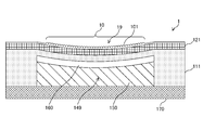
- FIG. 13 is a cross-sectional view illustrating a configuration example of an imaging element according to the fifth embodiment of the present disclosure.
- the imaging device 1 in FIG. 4 differs from the imaging device 1 described in FIG. 3 in that a cover 170 is disposed.
- the lid 170 in the figure limits the contraction of the curved holding section 150. Specifically, shrinkage on the back surface of the curved holding portion 150 is limited by disposing the lid portion 170. For this reason, the amount of shrinkage in the vicinity of the curved portion 160 can be improved. Thereby, formation of the curved portion 19 can be facilitated.
- As the lid 170 an inorganic substrate made of metal, Si, SiO 2 or the like, or an organic substrate made of resin or the like can be used.
- the lid 170 may be arranged, for example, by placing the liquid curved holding unit 150 in the concave portion 149 while adjusting the amount of application, and then placing the lid 170 on the back surface of the semiconductor substrate 111 and the curved holding unit 150. It can be carried out.
- the lid 170 may be adhered to the semiconductor substrate 111 before the application of the curved holding unit 150, and the liquid curved holding unit 150 may be applied through an opening formed in the lid 170.
- the adhesive for example, an ultraviolet-curable adhesive can be used.
- vacuum defoaming of the liquid curved holding unit 150 can be performed through the opening.
- the configuration of the image sensor 1 other than the above is the same as the configuration of the image sensor 1 described in the first embodiment of the present disclosure, and a description thereof will not be repeated.
- the shrinkage on the back surface of the bending holding unit 150 is limited, and the shrinkage amount near the bending forming unit 160 is reduced. Improve. Thus, the formation of the curved portion 19 can be easily performed.
- the curved portion 19 is formed by the curved portion 160.
- the imaging device 1 according to the sixth embodiment of the present disclosure differs from the above-described first embodiment in that the curvature forming section 160 is omitted.
- FIG. 14 is a cross-sectional view illustrating a configuration example of an imaging element according to the sixth embodiment of the present disclosure.
- the imaging device 1 in FIG. 3 differs from the imaging device 1 described in FIG. 3 in that the curvature forming section 160 is omitted.
- the curved holding section 150 is arranged in the concave portion 149 of the semiconductor substrate 111.
- the curved forming section 160 can be omitted.
- the lid 170 by further arranging the lid 170, the amount of contraction of the curved holding portion 150 in the vicinity of the wiring region 121 can be improved.
- the configuration of the image sensor 1 other than the above is the same as the configuration of the image sensor 1 described in the first embodiment of the present disclosure, and a description thereof will not be repeated.
- the bending portion 19 is formed on the imaging chip by the bending holding unit 150. Accordingly, the curved forming section 160 can be omitted, and the manufacturing process of the imaging device 1 can be further simplified.
- the image sensor 1 according to the first embodiment described above uses the curved holding section 150 made of resin.
- the imaging device 1 according to the seventh embodiment of the present disclosure is different from the first embodiment in that the holding base made of metal or the like is bonded to the semiconductor substrate 111 on which the curved portion 19 is formed. And form.
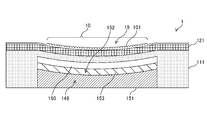
- FIG. 15 is a cross-sectional view illustrating a configuration example of an imaging element according to the seventh embodiment of the present disclosure.
- the imaging device 1 in FIG. 3 differs from the imaging device 1 described in FIG. 3 in that a holding base 151 and an adhesive portion 153 are arranged instead of the curved holding portion 150.
- the holding base 151 is disposed in the recess 149 and holds the curved portion 19 of the semiconductor substrate 111.
- the holding base 151 has a second concave portion 152 that fits into the curved portion 19, and is bonded to the curved forming portion 160 by the bonding portion 153.
- the holding base 151 can be made of, for example, metal, semiconductor, glass, and resin.
- the bonding portion 153 is for bonding the curved forming portion 160 and the holding base 151.
- An adhesive made of a thermosetting resin, a thermoplastic resin, or the like can be used for the bonding portion 153.
- the holding base 151 can be adhered to the curved portion 160 as follows. First, the second concave portion 152 that fits the assumed shape of the curved portion 19 is formed in the holding base 151. Next, the adhesive portion 153 is applied to the second concave portion 152 and fitted into the concave portion 149, so that the adhesive portion 153 applied to the holding base 151 is arranged adjacent to the curved forming portion 160. After that, by heating the image sensor 1, the curved portion 19 is formed on the semiconductor substrate 111 by the curved forming portion 160, and the bonding portion 153 is cured. Thereby, the semiconductor substrate 111 on which the curved portion 19 is formed and the holding base 151 can be bonded. After applying the bonding portion 153 on the side of the curve forming portion 160, the holding base 151 may be disposed in the concave portion 149 and heated.
- the holding substrate 151 on which the bonding portion 153 is applied is disposed in the concave portion 149 of the semiconductor substrate 111 on which the curved portion 19 is formed by heating the imaging element 1, and the holding substrate 151 is bonded to the curved forming portion 160.
- the configuration of the image sensor 1 other than the above is the same as the configuration of the image sensor 1 described in the first embodiment of the present disclosure, and a description thereof will not be repeated.
- the rigidity of the imaging device 1 can be improved by using the holding base 151 and the bonding portion 153 as the curved holding portion 150. .
- an imaging chip including a semiconductor chip having a concave portion formed on a back surface different from a light receiving surface for receiving light from a subject; A curved forming portion that is arranged in the concave portion and forms the curved portion by curving the imaging chip at the bottom of the concave portion; An image pickup device comprising: a curved holding section that holds the formed curved section.
- the curved holding unit is made of a thermosetting resin.
- the curved holding unit is formed of a thermosetting resin that contracts upon curing.
- the bending holding section includes a holding base in which a second concave portion that fits into the bending section is arranged, and an adhesive section that is arranged between the holding base and the bending forming section.
- the imaging device according to any one of (1) to (8), further including an etching prevention layer disposed at a bottom of the concave portion of the semiconductor chip to prevent etching of the semiconductor chip.
Landscapes
- Engineering & Computer Science (AREA)
- Multimedia (AREA)
- Signal Processing (AREA)
- Transforming Light Signals Into Electric Signals (AREA)
- Solid State Image Pick-Up Elements (AREA)
Abstract
撮影レンズの収差に応じて湾曲した受光面を有する撮像素子の製造方法を簡略化する。 撮像素子は、撮像チップと湾曲形成部と湾曲保持部とを具備する。撮像チップは、被写体からの光を受光する受光面とは異なる面である裏面に凹部が形成された半導体チップにより構成される。湾曲形成部は、その凹部に配置されてその凹部の底部におけるその撮像チップを湾曲させて湾曲部を形成する。湾曲保持部は、形成された湾曲部を保持する。
Description
本開示は、撮像素子および撮像素子の製造方法に関する。詳しくは、受光面を湾曲させた撮像素子および当該撮像素子の製造方法に関する。
従来、撮影レンズにより結像された被写体を撮像する固体撮像素子が収容された固体撮像装置が使用されている。撮影レンズには収差があり、平面形状の固体撮像素子に被写体を結像する際、固体撮像素子の中央部や端部にぼけを生じる問題がある。そこで、撮影レンズの収差に合わせて固体撮像素子を湾曲させることにより、中央部や端部におけるぼけの発生を防止する撮像装置が提案されている。例えば、固体撮像素子が形成される面である第1面および第1面の裏面である第2面を有する平板状の半導体基板と、平面形状の第3面および第3面の裏面であるとともに曲面形状の凹部が形成される第4面を有する樹脂層とを備える固体撮像装置が提案されている。この固体撮像装置においては、半導体基板の第2面および樹脂層の第3面が接着された後に樹脂層の第4面がパッケージに接着される。この際、樹脂層の第4面の凹部においてもパッケージに密着して接着することにより第4面の凹部の形状に合わせて樹脂層が変形し、固体撮像装置の第1面および第2面に凹部を形成することができる(例えば、特許文献1参照。)。
上述の従来技術は、樹脂層の凹部が形成された第4面をパッケージに密着させる際、第4面の凹部とパッケージとに囲まれた領域の空気をパッケージに形成された貫通孔を介して排気する。この工程により半導体基板に大気圧が加わり、曲面形状の凹部が形成される。このように、上述の従来技術では、パッケージ内の空気を排気する工程が必要となり、撮像装置の製造工程が複雑になるという問題がある。
本開示は、上述した問題点に鑑みてなされたものであり、撮影レンズの収差に応じて湾曲した受光面を有する撮像素子の製造方法を簡略化することを目的としている。
本開示は、上述の問題点を解消するためになされたものであり、その第1の態様は、被写体からの光を受光する受光面とは異なる面である裏面に凹部が形成された半導体チップにより構成される撮像チップと、上記凹部に配置されて上記凹部の底部における上記撮像チップを湾曲させて湾曲部を形成する湾曲形成部と、上記形成された湾曲部を保持する湾曲保持部とを具備する撮像素子である。
また、この第1の態様において、上記湾曲形成部は、上記撮像チップより高い線膨張率に構成されて加熱されることにより上記湾曲部を形成してもよい。
また、この第1の態様において、上記湾曲形成部は、金属により構成されてもよい。
また、この第1の態様において、上記湾曲保持部は、熱硬化性樹脂により構成されてもよい。
また、この第1の態様において、上記湾曲形成部は、上記湾曲保持部が硬化する際に上記湾曲部を形成してもよい。
また、この第1の態様において、上記湾曲保持部は硬化の際に収縮する熱硬化性樹脂により構成されてもよい。
また、この第1の態様において、上記湾曲保持部に隣接して配置されて上記凹部の開口部近傍における上記湾曲保持部の収縮を制限する蓋部を更に具備してもよい。
上記湾曲保持部は、上記湾曲部に嵌合する第2の凹部が配置される保持基体と当該保持基体および上記湾曲形成部の間に配置される接着部とにより構成されてもよい。
また、この第1の態様において、上記半導体チップにおける凹部の底部に配置されて上記半導体チップのエッチングを防止するエッチング防止層をさらに具備してもよい。
また、本開示の第2の態様は、半導体チップに構成される撮像チップにおける被写体からの光を受光する受光面とは異なる面である裏面に凹部を形成する凹部形成工程と、上記凹部の底部における上記撮像チップを湾曲させて湾曲部を形成する湾曲形成部により上記湾曲部を形成させる湾曲部形成工程と、上記形成された湾曲部を保持する湾曲保持部により上記湾曲部を保持させる湾曲部保持工程とを具備する撮像素子の製造方法である。
上述の態様を採ることにより、撮像チップの裏面に形成された凹部の底部近傍に湾曲形成部および湾曲保持部が配置され、撮像チップを裏面方向に湾曲させた状態に保持するという作用をもたらす。撮像チップ受光面における湾曲部の形成の簡略化が想定される。
本開示によれば、撮影レンズの収差に応じて湾曲した受光面を有する撮像素子の製造方法を簡略化するという優れた効果を奏する。
次に、図面を参照して、本開示を実施するための形態(以下、実施の形態と称する)を説明する。以下の図面において、同一または類似の部分には同一または類似の符号を付している。ただし、図面は、模式的なものであり、各部の寸法の比率等は現実のものとは必ずしも一致しない。また、図面相互間においても互いの寸法の関係や比率が異なる部分が含まれることは勿論である。また、以下の順序で実施の形態の説明を行う。
1.第1の実施の形態
2.第2の実施の形態
3.第3の実施の形態
4.第4の実施の形態
5.第5の実施の形態
6.第6の実施の形態
7.第7の実施の形態
1.第1の実施の形態
2.第2の実施の形態
3.第3の実施の形態
4.第4の実施の形態
5.第5の実施の形態
6.第6の実施の形態
7.第7の実施の形態
<1.第1の実施の形態>
[撮像素子の構成]
図1は、本開示の実施の形態に係る撮像素子の構成例を示すブロック図である。同図の撮像素子1は、画素アレイ部10と、垂直駆動部20と、カラム信号処理部30と、制御部40とを備える。
[撮像素子の構成]
図1は、本開示の実施の形態に係る撮像素子の構成例を示すブロック図である。同図の撮像素子1は、画素アレイ部10と、垂直駆動部20と、カラム信号処理部30と、制御部40とを備える。
画素アレイ部10は、画素100が2次元格子状に配置されて構成されたものである。ここで、画素100は、照射された光に応じた画像信号を生成するものである。この画素100は、照射された光に応じた電荷を生成する光電変換部を有する。また画素100は、画素回路をさらに有する。この画素回路は、光電変換部により生成された電荷に基づく画像信号を生成する。画像信号の生成は、後述する垂直駆動部20により生成された制御信号により制御される。画素アレイ部10には、信号線11および12がXYマトリクス状に配置される。信号線11は、画素100における画素回路の制御信号を伝達する信号線であり、画素アレイ部10の行毎に配置され、各行に配置される画素100に対して共通に配線される。信号線12は、画素100の画素回路により生成された画像信号を伝達する信号線であり、画素アレイ部10の列毎に配置され、各列に配置される画素100に対して共通に配線される。これら光電変換部および画素回路は、後述する半導体基板111および配線領域121に形成される。
垂直駆動部20は、画素100の画素回路の制御信号を生成するものである。この垂直駆動部20は、生成した制御信号を同図の信号線11を介して画素100に伝達する。カラム信号処理部30は、画素100により生成された画像信号を処理するものである。このカラム信号処理部30は、同図の信号線12を介して画素100から伝達された画像信号の処理を行う。カラム信号処理部30における処理には、例えば、画素100において生成されたアナログの画像信号をデジタルの画像信号に変換するアナログデジタル変換が該当する。カラム信号処理部30により処理された画像信号は、撮像素子1の画像信号として出力される。制御部40は、撮像素子1の全体を制御するものである。この制御部40は、垂直駆動部20およびカラム信号処理部30を制御する制御信号を生成して出力することにより、撮像素子1の制御を行う。制御部40により生成された制御信号は、信号線41および42により垂直駆動部20およびカラム信号処理部30に対してそれぞれ伝達される。
[撮像素子の外観]
図2は、本開示の実施の形態に係る撮像素子の構成例を示す図である。同図は、撮像素子1の構成例を表す外観図である。同図の撮像素子1は、被写体からの光を受光する面である受光面に図1において説明した画素アレイ部10が形成される。また、受光面とは異なる面である裏面に円柱形状の凹部149が形成される。後述するように、凹部149の底面は、同図の裏面方向に湾曲しており、この湾曲に合わせて画素アレイ部10も湾曲して構成される。これにより、撮影レンズの収差に基づく画質の低下を防止することができる。
図2は、本開示の実施の形態に係る撮像素子の構成例を示す図である。同図は、撮像素子1の構成例を表す外観図である。同図の撮像素子1は、被写体からの光を受光する面である受光面に図1において説明した画素アレイ部10が形成される。また、受光面とは異なる面である裏面に円柱形状の凹部149が形成される。後述するように、凹部149の底面は、同図の裏面方向に湾曲しており、この湾曲に合わせて画素アレイ部10も湾曲して構成される。これにより、撮影レンズの収差に基づく画質の低下を防止することができる。
なお、凹部149の形状はこの例に限定されない。例えば四角柱や八角柱の形状にすることもできる。
[撮像素子の断面の構成]
図3は、本開示の第1の実施の形態に係る撮像素子の構成例を示す断面図である。同図の撮像素子1は、半導体基板111と、配線領域121と、湾曲形成部160と、湾曲保持部150とを備える。
図3は、本開示の第1の実施の形態に係る撮像素子の構成例を示す断面図である。同図の撮像素子1は、半導体基板111と、配線領域121と、湾曲形成部160と、湾曲保持部150とを備える。
半導体基板111は、画素アレイ部10の半導体素子部分が形成される半導体の基板である。この半導体基板111は、例えば、シリコンにより構成することができる。図1において説明した光電変換部や画素回路および垂直駆動部20等が半導体基板111に形成される。この半導体基板111の表面に配線領域121が形成され、配線領域121の表面に不図示のカラーフィルタやオンチップレンズが配置される。カラーフィルタは、入射光のうちの所定の波長の光を透過させる光学的なフィルタであり、オンチップレンズは、画素100毎に配置されて入射光を集光するレンズである。同図の撮像素子1は、半導体基板111の表面側から画素100に入射光が照射される表面照射型の撮像素子に該当する。
また、半導体基板111の裏面には、図2において説明した凹部149が配置される。この凹部149は、例えば、半導体基板111をエッチングすることにより形成することができる。
配線領域121は、信号を伝達する配線が形成される領域である。この配線領域は、配線が形成される配線層と配線を絶縁する絶縁層とにより構成される。図1において説明した信号線11、12、41および42は、配線領域121に配置される。配線層は、例えば、銅(Cu)やアルミニウム(Al)等の金属により構成することができる。また、絶縁層は、例えば、酸化シリコン(SiO2)により構成することができる。
同図に表したように、半導体基板111および配線領域121には、裏面方向に湾曲した湾曲部19が配置される。なお、半導体基板111および配線領域121は、撮像チップを構成する。
湾曲形成部160は、凹部149に配置されて、半導体基板111および配線領域121を湾曲させて湾曲部19を形成するものである。この湾曲形成部160は半導体基板111や配線領域121よりも高い線膨張率の材料により構成することができる。上述のように半導体基板111をシリコン(Si)により構成し、配線領域121をSiO2による絶縁層およびCuやAlによる配線層により構成した場合には、湾曲形成部160として金属を使用することができる。例えば、Cu、Al、金(Au)、白金(Pt)、チタン(Ti)、ニッケル(Ni)およびタンタル(Ta)を湾曲形成部160として使用することができる。
湾曲形成部160を配置した後に半導体基板111、配線領域121および湾曲形成部160を加熱して膨張させる。この際、半導体基板111および配線領域121より湾曲形成部160の線膨張率が高いため、同図に表したように、裏面方向に半導体基板111および配線領域121を湾曲させることができる。また、湾曲形成部160を配置することにより、凹部149が形成された撮像チップの強度を向上させることができる。
湾曲保持部150は、湾曲部19を保持するものである。この湾曲保持部150は、湾曲部19が形成された凹部149に配置され、例えば、樹脂により構成することができる。湾曲保持部150を半導体基板111および配線領域121に接着することにより、湾曲状態を保ったまま湾曲部19を保持することができる。この湾曲保持部150には、光硬化性樹脂や熱硬化性樹脂を使用することができる。なお、湾曲保持部150を熱硬化性樹脂により構成すると好適である。湾曲保持部150を硬化させる際の加熱により、湾曲形成部160による湾曲部19の形成を行うことができるためである。具体的には、液状の湾曲保持部150を凹部149に配置し、撮像チップおよび湾曲形成部160および湾曲保持部150を湾曲保持部150の硬化温度まで加熱する。この加熱により、湾曲形成部160が膨張して湾曲部19が形成される。その後、湾曲保持部150が硬化する。湾曲保持部150が硬化するため、撮像チップの温度を室温に戻しても湾曲部19を保持することができる。なお、上述の湾曲形成部160は、湾曲保持部150の少なくとも一部が硬化する際に湾曲部19を形成することができる。
また、湾曲保持部150として、硬化の際に収縮する樹脂を使用することもできる。この場合には、湾曲形成部160に加えて湾曲保持部150の収縮により湾曲部19を形成することができる。
[撮像素子の断面の他の構成]
図4は、本開示の第1の実施の形態に係る撮像素子の他の構成例を示す断面図である。同図におけるaは、凹部149の底面および側面に湾曲形成部160が配置される例を表したものである。同図におけるbは、凹部149の底面および側面ならびに半導体基板111の裏面に湾曲形成部160が配置される例を表したものである。同図におけるcは、凹部149の底面および半導体基板111の裏面に湾曲形成部160が配置される例を表したものである。
図4は、本開示の第1の実施の形態に係る撮像素子の他の構成例を示す断面図である。同図におけるaは、凹部149の底面および側面に湾曲形成部160が配置される例を表したものである。同図におけるbは、凹部149の底面および側面ならびに半導体基板111の裏面に湾曲形成部160が配置される例を表したものである。同図におけるcは、凹部149の底面および半導体基板111の裏面に湾曲形成部160が配置される例を表したものである。
[撮像装置の構成]
図5は、本開示の第1の実施の形態に係る撮像装置の構成例を示す断面図である。同図におけるaは、撮像素子1が回路基板4に実装される例を表したものである。撮像素子1は、回路基板4にダイボンディングされ、ボンディングワイヤ3により撮像素子1および回路基板4が電気的に接続される。撮像素子1にはボンディングワイヤ3が接続されるパッド(不図示)が配置される。このパッドは、撮像素子1の周縁部に配置される。当該領域は湾曲部19の外側の領域であるため、回路基板4の実装面に平行な領域となる。このため、湾曲部19の影響を受けることなくワイヤボンディングを行うことができる。
図5は、本開示の第1の実施の形態に係る撮像装置の構成例を示す断面図である。同図におけるaは、撮像素子1が回路基板4に実装される例を表したものである。撮像素子1は、回路基板4にダイボンディングされ、ボンディングワイヤ3により撮像素子1および回路基板4が電気的に接続される。撮像素子1にはボンディングワイヤ3が接続されるパッド(不図示)が配置される。このパッドは、撮像素子1の周縁部に配置される。当該領域は湾曲部19の外側の領域であるため、回路基板4の実装面に平行な領域となる。このため、湾曲部19の影響を受けることなくワイヤボンディングを行うことができる。
同図におけるbは、撮影レンズ6およびアクチュエータ5が配置されるとともにCSP(Chip Size Package)に構成された撮像モジュールの例を表したものである。アクチュエータ5は、撮影レンズ6を駆動するものである。このアクチュエータ5は、保護ガラス7を介して撮像素子1に配置される。撮像素子1には受光面に湾曲部19が配置されるため、スペーサを省略することができ、接着剤等により保護ガラス7および撮像素子1を直接接着することができる。なお、保護ガラス7および撮像素子1の間にスペーサを配置することもできる。撮像素子1の裏面には半田バンプ129が配置される。配線領域121および半田バンプ129はビア128により接続される。
[湾曲量]
図6は、本開示の第1の実施の形態に係る湾曲の一例を示す図である。同図は、湾曲形成部160の厚さと湾曲量との関係を表す図である。ここで湾曲量とは、受光面における撮像素子1の表面を基準とした湾曲部19の反り量の最大値を表す。同図の実線のグラフ301および点線のグラフ302は、それぞれ加熱温度160℃および200℃の場合の湾曲形成部160の厚さと湾曲量との関係を表すグラフである。同図に表したように、湾曲形成部の厚みを変化させることにより、湾曲量を変化させることができる。また、同図に表したように湾曲量には極大値が存在する。そこで、所望の湾曲量がグラフの極大値近傍になるように硬化温度等を調整することができ、湾曲形成部160の厚みの誤差の影響を受けにくい構成にすることができる。
図6は、本開示の第1の実施の形態に係る湾曲の一例を示す図である。同図は、湾曲形成部160の厚さと湾曲量との関係を表す図である。ここで湾曲量とは、受光面における撮像素子1の表面を基準とした湾曲部19の反り量の最大値を表す。同図の実線のグラフ301および点線のグラフ302は、それぞれ加熱温度160℃および200℃の場合の湾曲形成部160の厚さと湾曲量との関係を表すグラフである。同図に表したように、湾曲形成部の厚みを変化させることにより、湾曲量を変化させることができる。また、同図に表したように湾曲量には極大値が存在する。そこで、所望の湾曲量がグラフの極大値近傍になるように硬化温度等を調整することができ、湾曲形成部160の厚みの誤差の影響を受けにくい構成にすることができる。
[撮像素子の製造方法]
図7および8は、本開示の第1の実施の形態に係る撮像素子の製造方法の一例を示す図である。図7および8は、撮像素子1の製造工程の一例を表す図である。
図7および8は、本開示の第1の実施の形態に係る撮像素子の製造方法の一例を示す図である。図7および8は、撮像素子1の製造工程の一例を表す図である。
まず、半導体基板111に光電変換部や画素回路等の半導体素子を形成し、配線領域121を形成する(図7におけるa)。次に、配線領域121の表面にカラーフィルタ(不図示)およびオンチップレンズ101を配置する(図7におけるb)。
次に、半導体基板111の裏面に凹部149を形成する(図7におけるc)。これは、エッチングにより行うことができる。具体的には、凹部149を配置する位置に開口部を有するレジスト等によるマスクを半導体基板111の裏面に形成し、水酸化カリウム等の水溶液を噴霧してエッチングすることにより行うことができる。また、半導体基板111のエッチングは、ドライエッチングにより行うこともできる。当該工程は、請求の範囲に記載の凹部形成工程の一例である。
次に、凹部149に湾曲形成部160を配置する(図8におけるd)。これは、例えば、スパッタリングやめっきにより行うことができる。次に、凹部149に湾曲保持部150を配置する(図8におけるe)。これは、例えば、湾曲保持部150の材料となる液状の樹脂をディスペンサ等により凹部149に塗布することにより行うことができる。なお、図8におけるeの撮像素子1の天地を反転させて液状の樹脂を塗布することにより、塗布した液状の樹脂の保持が可能になる。
次に、撮像素子チップを加熱する。これにより、湾曲形成部160により湾曲部19が形成される。当該工程は、請求の範囲に記載の湾曲部形成工程の一例である。その後、湾曲保持部150が硬化し、形成された湾曲部19が保持される(図8におけるf)。当該工程は、請求の範囲に記載の湾曲部保持工程の一例である。以上説明した工程により、撮像素子1を製造することができる。
以上説明したように、本開示の第1の実施の形態の撮像素子1は、撮像素子チップより線膨張率が高い湾曲形成部160を半導体チップの凹部149に配置し、加熱することにより湾曲部19を形成する。その後、湾曲保持部150により形成された湾曲部19を保持させる。これにより、湾曲部19を有する撮像素子1の製造工程を簡略化することができる。
<2.第2の実施の形態>
上述の第1の実施の形態の撮像素子1は、表面照射型の撮像素子により構成されていた。これに対し、本開示の第2の実施の形態の撮像素子1は、裏面照射型の撮像素子により構成される点で、上述の第1の実施の形態と異なる。
上述の第1の実施の形態の撮像素子1は、表面照射型の撮像素子により構成されていた。これに対し、本開示の第2の実施の形態の撮像素子1は、裏面照射型の撮像素子により構成される点で、上述の第1の実施の形態と異なる。
[撮像素子の断面の構成]
図9は、本開示の第2の実施の形態に係る撮像素子の構成例を示す断面図である。同図の撮像素子1は、半導体基板111および配線領域121が入れ替わった構成の撮像素子1を使用する点で、図3において説明した撮像素子1と異なる。すなわち、同図の撮像素子1は、半導体基板111の表面(同図における下面)に配線領域121が配置され、この面とは異なる面である裏面にカラーフィルタやオンチップレンズ101が配置されて入射光が照射される。このような構成の撮像素子1は、裏面照射型の撮像素子と称される。また、同図の撮像素子1は、配線領域121に隣接して支持基板141が配置され、支持基板141に凹部149が形成される点で、図3において説明した撮像素子1と異なる。
図9は、本開示の第2の実施の形態に係る撮像素子の構成例を示す断面図である。同図の撮像素子1は、半導体基板111および配線領域121が入れ替わった構成の撮像素子1を使用する点で、図3において説明した撮像素子1と異なる。すなわち、同図の撮像素子1は、半導体基板111の表面(同図における下面)に配線領域121が配置され、この面とは異なる面である裏面にカラーフィルタやオンチップレンズ101が配置されて入射光が照射される。このような構成の撮像素子1は、裏面照射型の撮像素子と称される。また、同図の撮像素子1は、配線領域121に隣接して支持基板141が配置され、支持基板141に凹部149が形成される点で、図3において説明した撮像素子1と異なる。
支持基板141は、半導体基板111および配線領域121を支持する基板である。この支持基板141は、撮像素子1の製造工程において、半導体基板111等の強度を向上させるものである。支持基板141は、例えば、半導体やガラスの基板により構成することができる。なお、同図の支持基板141には、凹部149が配置される。この凹部149は、支持基板141をエッチングすることにより形成することができる。
同図の撮像素子1の製造方法について説明する。まず、半導体基板111に光電変換部や画素回路等の半導体素子を形成し、半導体基板111の表面に配線領域121を形成する。次に、配線領域121に隣接して支持基板141を貼り合わせる。次に、半導体基板111の天地を反転させて半導体基板111を研削し、薄肉化する。薄肉化は、例えば、化学的機械的研磨(CMP:Chemical Mechanical Polishing)により行うことができる。次に、半導体基板111の表面にカラーフィルタおよびオンチップレンズ101を配置する。次に、支持基板141に凹部149を形成し、湾曲形成部160および湾曲保持部150を順に配置する。
なお、半導体基板111には、配線領域121を配置する前に、剥離を容易化する埋め込み層を形成することもできる。半導体基板111の薄肉化の際、埋め込み層の部分において半導体基板111の裏面側の引き剥がしを行う。その後、引き剥がし面を研削して薄肉化することにより、半導体基板111の研削を簡略化することができる。
これ以外の撮像素子1の構成は本開示の第1の実施の形態において説明した撮像素子1の構成と同様であるため、説明を省略する。
以上説明したように、本開示の第2の実施の形態の撮像素子1は、裏面照射型の撮像素子に構成され、支持基板141に凹部149が形成されて湾曲形成部160および湾曲保持部150が配置される。これにより、裏面照射型の撮像素子を採用する撮像素子1の製造工程を簡略化することができる。
<3.第3の実施の形態>
上述の第2の実施の形態の撮像素子1は、単一の半導体基板111により構成されていた。これに対し、本開示の第3の実施の形態の撮像素子1は、複数の半導体基板が貼り合わされて構成される点で、上述の第2の実施の形態と異なる。
上述の第2の実施の形態の撮像素子1は、単一の半導体基板111により構成されていた。これに対し、本開示の第3の実施の形態の撮像素子1は、複数の半導体基板が貼り合わされて構成される点で、上述の第2の実施の形態と異なる。
[撮像素子の断面の構成]
図10は、本開示の第3の実施の形態に係る撮像素子の構成例を示す断面図である。同図の撮像素子1は、支持基板141の代わりに半導体基板112および配線領域122が配置され、半導体基板112に凹部149が形成される点で、図9において説明した撮像素子1と異なる。
図10は、本開示の第3の実施の形態に係る撮像素子の構成例を示す断面図である。同図の撮像素子1は、支持基板141の代わりに半導体基板112および配線領域122が配置され、半導体基板112に凹部149が形成される点で、図9において説明した撮像素子1と異なる。
同図の撮像素子1は、画素アレイ部10が形成される半導体基板111と半導体基板112とが配線領域121と配線領域122を介して貼り合わされて構成される。半導体基板112には、例えば、図1において説明したカラム信号処理部30を配置することができる。半導体基板111に配置される画素回路は、アナログの画像信号を取り扱うとともに比較的低速に動作する。一方、カラム信号処理部30は、アナログの画像信号をデジタルの画像信号に変換するアナログデジタル変換部が配置され、比較的高速に動作する。そこで、これらの回路を異なる基板に形成することにより、最適なプロセスを選択することができる。半導体基板111の配線領域121と半導体基板112の配線領域122との間において貼り合わせが行われる。
この貼り合わせには、公知の技術を適用することができる。具体的には、配線領域121および配線領域122の貼合せ面にCu等による金属コンタクト部を形成し、貼り合せの際にこの金属コンタクト部同士を接合させる。これにより、機械的および電気的に半導体基板111および半導体基板112の配線領域同士を接続することができる。
前述のように、凹部149は、半導体チップの裏面に配置される。同図の撮像素子1においては、半導体基板112に凹部149が形成される。この凹部149に湾曲形成部160および湾曲保持部150が更に配置され、湾曲部19が形成されて保持される。
なお、撮像素子1の構成は、この例に限定されない。例えば、3つ以上の半導体基板が貼り合わされた構成にすることもできる。
これ以外の撮像素子1の構成は本開示の第1の実施の形態において説明した撮像素子1の構成と同様であるため、説明を省略する。
以上説明したように、本開示の第3の実施の形態の撮像素子1は、複数の半導体基板が貼り合わされて構成され、裏面側の端面に配置される半導体基板に凹部149が形成される。これにより、複数の半導体基板が貼り合わされて構成された撮像素子1において湾曲部19を形成することができる。
<4.第4の実施の形態>
上述の第3の実施の形態の撮像素子1は、半導体基板112をエッチングすることにより凹部149を形成していた。これに対し、本開示の第4の実施の形態の撮像素子1は、エッチングを防止するエッチング防止層が配置される点で、上述の第3の実施の形態と異なる。
上述の第3の実施の形態の撮像素子1は、半導体基板112をエッチングすることにより凹部149を形成していた。これに対し、本開示の第4の実施の形態の撮像素子1は、エッチングを防止するエッチング防止層が配置される点で、上述の第3の実施の形態と異なる。
[撮像素子の断面の構成]
図11は、本開示の第4の実施の形態に係る撮像素子の構成例を示す断面図である。同図の撮像素子1は、凹部149が配線領域122に隣接して配置される点で、図10において説明した撮像素子1と異なる。すなわち、同図の撮像素子1は、配線領域122を半導体基板112のエッチング防止層として使用し、配線領域122との界面まで半導体基板112のエッチングを行う。
図11は、本開示の第4の実施の形態に係る撮像素子の構成例を示す断面図である。同図の撮像素子1は、凹部149が配線領域122に隣接して配置される点で、図10において説明した撮像素子1と異なる。すなわち、同図の撮像素子1は、配線領域122を半導体基板112のエッチング防止層として使用し、配線領域122との界面まで半導体基板112のエッチングを行う。
同図の配線領域122は、凹部149を形成する際のエッチングを止めるものである。配線領域122により半導体基板112のエッチングが停止されるため、エッチング量の管理を省略することができ、撮像素子1の製造工程を簡略化することができる。その後、配線領域122に隣接して湾曲形成部160が形成される。
[撮像素子の断面の他の構成]
図12は、本開示の第4の実施の形態に係る撮像素子の他の構成例を示す断面図である。同図は、半導体基板112および配線領域122の代わりに支持基板141を配置する場合の例を表したものである。同図の撮像素子1においては、配線領域121をエッチング防止層として使用することができる。
図12は、本開示の第4の実施の形態に係る撮像素子の他の構成例を示す断面図である。同図は、半導体基板112および配線領域122の代わりに支持基板141を配置する場合の例を表したものである。同図の撮像素子1においては、配線領域121をエッチング防止層として使用することができる。
なお、図11における配線領域122および図12における配線領域121は、請求の範囲に記載のエッチング防止層の一例である。
これ以外の撮像素子1の構成は本開示の第1の実施の形態において説明した撮像素子1の構成と同様であるため、説明を省略する。
以上説明したように、本開示の第4の実施の形態の撮像素子1は、配線領域122および121をエッチング防止層として使用することにより、半導体基板112および支持基板141のエッチングにおいて、エッチング量を制御することができる。これにより、撮像素子1の製造工程を簡略化することができる。
<5.第5の実施の形態>
上述の第1の実施の形態の撮像素子1は、湾曲保持部150の裏面側が解放されていた。これに対し、本開示の第5の実施の形態の撮像素子1は、湾曲保持部150の裏面側に蓋部が配置される点で、上述の第1の実施の形態と異なる。
上述の第1の実施の形態の撮像素子1は、湾曲保持部150の裏面側が解放されていた。これに対し、本開示の第5の実施の形態の撮像素子1は、湾曲保持部150の裏面側に蓋部が配置される点で、上述の第1の実施の形態と異なる。
[撮像素子の断面の構成]
図13は、本開示の第5の実施の形態に係る撮像素子の構成例を示す断面図である。同図の撮像素子1は、蓋部170が配置される点で、図3において説明した撮像素子1と異なる。
図13は、本開示の第5の実施の形態に係る撮像素子の構成例を示す断面図である。同図の撮像素子1は、蓋部170が配置される点で、図3において説明した撮像素子1と異なる。
同図の蓋部170は、湾曲保持部150の収縮を制限するものである。具体的には、蓋部170を配置することにより、湾曲保持部150の裏面における収縮を制限する。このため、湾曲形成部160近傍において収縮量を向上させることができる。これにより、湾曲部19の形成を容易なものにすることができる。この蓋部170には、金属、SiおよびSiO2等により構成された無機基板や樹脂等により構成された有機基板を使用することができる。なお、蓋部170の配置は、例えば、塗布量を調整しながら液状の湾曲保持部150を凹部149に配置した後に蓋部170を半導体基板111および湾曲保持部150の裏面に載置することにより行うことができる。また、例えば、湾曲保持部150の塗布前に蓋部170を半導体基板111に接着し、蓋部170に形成された開口部を介して液状の湾曲保持部150を塗布することもできる。この接着剤には、例えば、紫外光硬化型の接着剤を使用することができる。また、開口部を介して液状の湾曲保持部150の真空脱泡を行うこともできる。
これ以外の撮像素子1の構成は本開示の第1の実施の形態において説明した撮像素子1の構成と同様であるため、説明を省略する。
以上説明したように、本開示の第5の実施の形態の撮像素子1は、蓋部170を配置することにより、湾曲保持部150の裏面における収縮を制限して湾曲形成部160近傍において収縮量を向上させる。これにより、湾曲部19の形成を容易に行うことができる。
<6.第6の実施の形態>
上述の第1の実施の形態の撮像素子1は、湾曲形成部160により湾曲部19を形成していた。これに対し、本開示の第6の実施の形態の撮像素子1は、湾曲形成部160を省略する点で、上述の第1の実施の形態と異なる。
上述の第1の実施の形態の撮像素子1は、湾曲形成部160により湾曲部19を形成していた。これに対し、本開示の第6の実施の形態の撮像素子1は、湾曲形成部160を省略する点で、上述の第1の実施の形態と異なる。
[撮像素子の断面の構成]
図14は、本開示の第6の実施の形態に係る撮像素子の構成例を示す断面図である。同図の撮像素子1は、湾曲形成部160を省略する点で、図3において説明した撮像素子1と異なる。
図14は、本開示の第6の実施の形態に係る撮像素子の構成例を示す断面図である。同図の撮像素子1は、湾曲形成部160を省略する点で、図3において説明した撮像素子1と異なる。
同図の撮像素子1においては、半導体基板111の凹部149には、湾曲保持部150のみが配置される。この湾曲保持部150として硬化収縮性を有する樹脂を使用することにより、湾曲形成部160を省略することができる。また、蓋部170をさらに配置することにより、配線領域121近傍における湾曲保持部150の収縮量を向上させることができる。
これ以外の撮像素子1の構成は本開示の第1の実施の形態において説明した撮像素子1の構成と同様であるため、説明を省略する。
以上説明したように、本開示の第6の実施の形態の撮像素子1は、湾曲保持部150により撮像チップに湾曲部19を形成する。これにより、湾曲形成部160を省略することができ、撮像素子1の製造工程をさらに簡略化することができる。
<7.第7の実施の形態>
上述の第1の実施の形態の撮像素子1は、樹脂により構成された湾曲保持部150を使用していた。これに対し、本開示の第7の実施の形態の撮像素子1は、金属等により構成された保持基体を湾曲部19が形成された半導体基板111に接着する点で、上述の第1の実施の形態と異なる。
上述の第1の実施の形態の撮像素子1は、樹脂により構成された湾曲保持部150を使用していた。これに対し、本開示の第7の実施の形態の撮像素子1は、金属等により構成された保持基体を湾曲部19が形成された半導体基板111に接着する点で、上述の第1の実施の形態と異なる。
[撮像素子の断面の構成]
図15は、本開示の第7の実施の形態に係る撮像素子の構成例を示す断面図である。同図の撮像素子1は、湾曲保持部150の代わりに保持基体151および接着部153を配置する点で、図3において説明した撮像素子1と異なる。
図15は、本開示の第7の実施の形態に係る撮像素子の構成例を示す断面図である。同図の撮像素子1は、湾曲保持部150の代わりに保持基体151および接着部153を配置する点で、図3において説明した撮像素子1と異なる。
保持基体151は、凹部149に配置されて半導体基板111の湾曲部19を保持するものである。この保持基体151は、湾曲部19に嵌合する第2の凹部152が形成され、接着部153により湾曲形成部160に接着される。保持基体151は、例えば、金属、半導体、ガラスおよび樹脂により構成することができる。保持基体151を凹部149に配置することにより、撮像素子1の剛性を向上させることができる。
接着部153は、湾曲形成部160および保持基体151を接着するものである。この接着部153には、熱硬化性樹脂や熱可塑性樹脂等により構成される接着剤を使用することができる。
保持基体151の湾曲形成部160への接着は、次のように行うことができる。まず、想定される湾曲部19の形状に嵌合する第2の凹部152を保持基体151に形成する。次に、接着部153を第2の凹部152に塗布して凹部149にはめ込むことにより、保持基体151に塗布された接着部153を湾曲形成部160に隣接して配置する。その後、撮像素子1を加熱することにより、湾曲形成部160により半導体基板111に湾曲部19が形成されるとともに接着部153を硬化させる。これにより、湾曲部19が形成された半導体基板111と保持基体151とを接着することができる。なお、接着部153を湾曲形成部160の側に塗布した後、保持基体151を凹部149に配置して加熱することもできる。
また、撮像素子1を加熱することにより湾曲部19が形成された半導体基板111の凹部149に接着部153が塗布された保持基体151を配置し、湾曲形成部160に保持基体151を接着させることもできる。
これ以外の撮像素子1の構成は本開示の第1の実施の形態において説明した撮像素子1の構成と同様であるため、説明を省略する。
以上説明したように、本開示の第7の実施の形態の撮像素子1は、保持基体151および接着部153を湾曲保持部150として使用することにより、撮像素子1の剛性を向上させることができる。
最後に、上述した各実施の形態の説明は本開示の一例であり、本開示は上述の実施の形態に限定されることはない。このため、上述した各実施の形態以外であっても、本開示に係る技術的思想を逸脱しない範囲であれば、設計等に応じて種々の変更が可能であることは勿論である。
なお、本技術は以下のような構成もとることができる。
(1)被写体からの光を受光する受光面とは異なる面である裏面に凹部が形成された半導体チップにより構成される撮像チップと、
前記凹部に配置されて前記凹部の底部における前記撮像チップを湾曲させて湾曲部を形成する湾曲形成部と、
前記形成された湾曲部を保持する湾曲保持部と
を具備する撮像素子。
(2)前記湾曲形成部は、前記撮像チップより高い線膨張率に構成されて加熱されることにより前記湾曲部を形成する前記(1)に記載の撮像素子。
(3)前記湾曲形成部は、金属により構成される前記(2)に記載の撮像素子。
(4)前記湾曲保持部は、熱硬化性樹脂により構成される前記(2)に記載の撮像素子。
(5)前記湾曲形成部は、前記湾曲保持部が硬化する際に前記湾曲部を形成する前記(4)に記載の撮像素子。
(6)前記湾曲保持部は、硬化の際に収縮する熱硬化性樹脂により構成される前記(4)に記載の撮像素子。
(7)前記湾曲保持部に隣接して配置されて前記凹部の開口部近傍における前記湾曲保持部の収縮を制限する蓋部を更に具備する前記(6)に記載の撮像素子。
(8)前記湾曲保持部は、前記湾曲部に嵌合する第2の凹部が配置される保持基体と当該保持基体および前記湾曲形成部の間に配置される接着部とにより構成される前記(1)から(7)の何れかに記載の撮像素子。
(9)前記半導体チップにおける凹部の底部に配置されて前記半導体チップのエッチングを防止するエッチング防止層をさらに具備する前記(1)から(8)の何れかに記載の撮像素子。
(10)半導体チップに構成される撮像チップにおける被写体からの光を受光する受光面とは異なる面である裏面に凹部を形成する凹部形成工程と、
前記凹部の底部における前記撮像チップを湾曲させて湾曲部を形成する湾曲形成部により前記湾曲部を形成させる湾曲部形成工程と、
前記形成された湾曲部を保持する湾曲保持部により前記湾曲部を保持させる湾曲部保持工程と
を具備する撮像素子の製造方法。
(1)被写体からの光を受光する受光面とは異なる面である裏面に凹部が形成された半導体チップにより構成される撮像チップと、
前記凹部に配置されて前記凹部の底部における前記撮像チップを湾曲させて湾曲部を形成する湾曲形成部と、
前記形成された湾曲部を保持する湾曲保持部と
を具備する撮像素子。
(2)前記湾曲形成部は、前記撮像チップより高い線膨張率に構成されて加熱されることにより前記湾曲部を形成する前記(1)に記載の撮像素子。
(3)前記湾曲形成部は、金属により構成される前記(2)に記載の撮像素子。
(4)前記湾曲保持部は、熱硬化性樹脂により構成される前記(2)に記載の撮像素子。
(5)前記湾曲形成部は、前記湾曲保持部が硬化する際に前記湾曲部を形成する前記(4)に記載の撮像素子。
(6)前記湾曲保持部は、硬化の際に収縮する熱硬化性樹脂により構成される前記(4)に記載の撮像素子。
(7)前記湾曲保持部に隣接して配置されて前記凹部の開口部近傍における前記湾曲保持部の収縮を制限する蓋部を更に具備する前記(6)に記載の撮像素子。
(8)前記湾曲保持部は、前記湾曲部に嵌合する第2の凹部が配置される保持基体と当該保持基体および前記湾曲形成部の間に配置される接着部とにより構成される前記(1)から(7)の何れかに記載の撮像素子。
(9)前記半導体チップにおける凹部の底部に配置されて前記半導体チップのエッチングを防止するエッチング防止層をさらに具備する前記(1)から(8)の何れかに記載の撮像素子。
(10)半導体チップに構成される撮像チップにおける被写体からの光を受光する受光面とは異なる面である裏面に凹部を形成する凹部形成工程と、
前記凹部の底部における前記撮像チップを湾曲させて湾曲部を形成する湾曲形成部により前記湾曲部を形成させる湾曲部形成工程と、
前記形成された湾曲部を保持する湾曲保持部により前記湾曲部を保持させる湾曲部保持工程と
を具備する撮像素子の製造方法。
1 撮像素子
4 回路基板
5 アクチュエータ
6 撮影レンズ
7 保護ガラス
10 画素アレイ部
19 湾曲部
11、12、41、42 信号線
20 垂直駆動部
30 カラム信号処理部
40 制御部
100 画素
101 オンチップレンズ
111、112 半導体基板
121、122 配線領域
141 支持基板
149 凹部
151 保持基体
152 第2の凹部
153 接着部
150 湾曲保持部
160 湾曲形成部
170 蓋部
4 回路基板
5 アクチュエータ
6 撮影レンズ
7 保護ガラス
10 画素アレイ部
19 湾曲部
11、12、41、42 信号線
20 垂直駆動部
30 カラム信号処理部
40 制御部
100 画素
101 オンチップレンズ
111、112 半導体基板
121、122 配線領域
141 支持基板
149 凹部
151 保持基体
152 第2の凹部
153 接着部
150 湾曲保持部
160 湾曲形成部
170 蓋部
Claims (10)
- 被写体からの光を受光する受光面とは異なる面である裏面に凹部が形成された半導体チップにより構成される撮像チップと、
前記凹部に配置されて前記凹部の底部における前記撮像チップを湾曲させて湾曲部を形成する湾曲形成部と、
前記形成された湾曲部を保持する湾曲保持部と
を具備する撮像素子。 - 前記湾曲形成部は、前記撮像チップより高い線膨張率に構成されて加熱されることにより前記湾曲部を形成する請求項1記載の撮像素子。
- 前記湾曲形成部は、金属により構成される請求項2記載の撮像素子。
- 前記湾曲保持部は、熱硬化性樹脂により構成される請求項2記載の撮像素子。
- 前記湾曲形成部は、前記湾曲保持部が硬化する際に前記湾曲部を形成する請求項4記載の撮像素子。
- 前記湾曲保持部は、硬化の際に収縮する熱硬化性樹脂により構成される請求項4記載の撮像素子。
- 前記湾曲保持部に隣接して配置されて前記凹部の開口部近傍における前記湾曲保持部の収縮を制限する蓋部を更に具備する請求項6記載の撮像素子。
- 前記湾曲保持部は、前記湾曲部に嵌合する第2の凹部が配置される保持基体と当該保持基体および前記湾曲形成部の間に配置される接着部とにより構成される請求項1記載の撮像素子。
- 前記半導体チップにおける凹部の底部に配置されて前記半導体チップのエッチングを防止するエッチング防止層をさらに具備する請求項1記載の撮像素子。
- 半導体チップに構成される撮像チップにおける被写体からの光を受光する受光面とは異なる面である裏面に凹部を形成する凹部形成工程と、
前記凹部の底部における前記撮像チップを湾曲させて湾曲部を形成する湾曲形成部により前記湾曲部を形成させる湾曲部形成工程と、
前記形成された湾曲部を保持する湾曲保持部により前記湾曲部を保持させる湾曲部保持工程と
を具備する撮像素子の製造方法。
Priority Applications (2)
| Application Number | Priority Date | Filing Date | Title |
|---|---|---|---|
| US17/250,730 US20210210540A1 (en) | 2018-09-07 | 2019-08-09 | Imaging element and method of manufacturing imaging element |
| JP2020541088A JP7401441B2 (ja) | 2018-09-07 | 2019-08-09 | 撮像素子および撮像素子の製造方法 |
Applications Claiming Priority (2)
| Application Number | Priority Date | Filing Date | Title |
|---|---|---|---|
| JP2018-167600 | 2018-09-07 | ||
| JP2018167600 | 2018-09-07 |
Publications (1)
| Publication Number | Publication Date |
|---|---|
| WO2020049953A1 true WO2020049953A1 (ja) | 2020-03-12 |
Family
ID=69722486
Family Applications (1)
| Application Number | Title | Priority Date | Filing Date |
|---|---|---|---|
| PCT/JP2019/031553 Ceased WO2020049953A1 (ja) | 2018-09-07 | 2019-08-09 | 撮像素子および撮像素子の製造方法 |
Country Status (3)
| Country | Link |
|---|---|
| US (1) | US20210210540A1 (ja) |
| JP (1) | JP7401441B2 (ja) |
| WO (1) | WO2020049953A1 (ja) |
Citations (3)
| Publication number | Priority date | Publication date | Assignee | Title |
|---|---|---|---|---|
| JP2012114189A (ja) * | 2010-11-24 | 2012-06-14 | Sony Corp | 固体撮像装置とその製造方法、並びに電子機器 |
| JP2012182243A (ja) * | 2011-02-28 | 2012-09-20 | Sony Corp | 固体撮像素子の製造方法、固体撮像素子、および電子機器 |
| JP2015192074A (ja) * | 2014-03-28 | 2015-11-02 | ソニー株式会社 | 固体撮像装置、電子機器、および固体撮像装置の製造方法 |
Family Cites Families (5)
| Publication number | Priority date | Publication date | Assignee | Title |
|---|---|---|---|---|
| JP2007266380A (ja) * | 2006-03-29 | 2007-10-11 | Matsushita Electric Ind Co Ltd | 半導体撮像装置およびその製造方法 |
| KR101378418B1 (ko) * | 2007-11-01 | 2014-03-27 | 삼성전자주식회사 | 이미지센서 모듈 및 그 제조방법 |
| JP5720304B2 (ja) | 2011-02-28 | 2015-05-20 | ソニー株式会社 | 固体撮像装置及び電子機器 |
| US8878116B2 (en) * | 2011-02-28 | 2014-11-04 | Sony Corporation | Method of manufacturing solid-state imaging element, solid-state imaging element and electronic apparatus |
| KR102468262B1 (ko) * | 2017-06-30 | 2022-11-18 | 에스케이하이닉스 주식회사 | 커브드 이미지 센서 |
-
2019
- 2019-08-09 WO PCT/JP2019/031553 patent/WO2020049953A1/ja not_active Ceased
- 2019-08-09 US US17/250,730 patent/US20210210540A1/en not_active Abandoned
- 2019-08-09 JP JP2020541088A patent/JP7401441B2/ja active Active
Patent Citations (3)
| Publication number | Priority date | Publication date | Assignee | Title |
|---|---|---|---|---|
| JP2012114189A (ja) * | 2010-11-24 | 2012-06-14 | Sony Corp | 固体撮像装置とその製造方法、並びに電子機器 |
| JP2012182243A (ja) * | 2011-02-28 | 2012-09-20 | Sony Corp | 固体撮像素子の製造方法、固体撮像素子、および電子機器 |
| JP2015192074A (ja) * | 2014-03-28 | 2015-11-02 | ソニー株式会社 | 固体撮像装置、電子機器、および固体撮像装置の製造方法 |
Also Published As
| Publication number | Publication date |
|---|---|
| JP7401441B2 (ja) | 2023-12-19 |
| US20210210540A1 (en) | 2021-07-08 |
| JPWO2020049953A1 (ja) | 2021-08-12 |
Similar Documents
| Publication | Publication Date | Title |
|---|---|---|
| JP4160083B2 (ja) | 光学装置用モジュール及び光学装置用モジュールの製造方法 | |
| JP5724322B2 (ja) | 固体撮像装置の製造方法 | |
| JP5709435B2 (ja) | 撮像モジュール及びカメラ | |
| US8790950B2 (en) | Method of manufacturing optical sensor, optical sensor, and camera including optical sensor | |
| US20050099532A1 (en) | Image pickup device and a manufacturing method thereof | |
| US10446598B2 (en) | Semiconductor device, manufacturing method, and electronic apparatus | |
| CN109979891B (zh) | 晶片级芯片尺寸封装结构 | |
| JP6067262B2 (ja) | 半導体装置およびその製造方法、ならびにカメラ | |
| JP2007266380A (ja) | 半導体撮像装置およびその製造方法 | |
| JP2011018747A (ja) | 撮像ユニット | |
| WO2015146332A1 (ja) | 固体撮像装置、電子機器、および固体撮像装置の製造方法 | |
| JP5720305B2 (ja) | 固体撮像素子の製造方法、固体撮像素子、および電子機器 | |
| CN113132585B (zh) | 感光芯片组件、移动终端、摄像模组及其制备方法 | |
| JP5720306B2 (ja) | 固体撮像素子の製造方法 | |
| US10916578B2 (en) | Semiconductor apparatus and camera | |
| JP4486005B2 (ja) | 半導体撮像装置およびその製造方法 | |
| JP2005064060A (ja) | 固体撮像素子、固体撮像素子の製造方法及び固体撮像装置 | |
| JP4466552B2 (ja) | 固体撮像装置の製造方法 | |
| JP7401441B2 (ja) | 撮像素子および撮像素子の製造方法 | |
| JP2002222935A (ja) | 固体撮像装置およびその製造方法、固体撮像システム | |
| US20090315130A1 (en) | Solid-state imaging apparatus and method for manufacturing the same | |
| JP2011066093A (ja) | 撮像ユニット | |
| WO2022085326A1 (ja) | 撮像装置、電子機器および撮像装置の製造方法 | |
| WO2015122299A1 (ja) | 固体撮像装置、電子機器、および固体撮像装置の製造方法 | |
| JP2002100751A (ja) | 固体撮像装置 |
Legal Events
| Date | Code | Title | Description |
|---|---|---|---|
| 121 | Ep: the epo has been informed by wipo that ep was designated in this application |
Ref document number: 19857937 Country of ref document: EP Kind code of ref document: A1 |
|
| ENP | Entry into the national phase |
Ref document number: 2020541088 Country of ref document: JP Kind code of ref document: A |
|
| NENP | Non-entry into the national phase |
Ref country code: DE |
|
| 122 | Ep: pct application non-entry in european phase |
Ref document number: 19857937 Country of ref document: EP Kind code of ref document: A1 |