WO2020031560A1 - 撮像装置及び制御方法 - Google Patents
撮像装置及び制御方法 Download PDFInfo
- Publication number
- WO2020031560A1 WO2020031560A1 PCT/JP2019/026363 JP2019026363W WO2020031560A1 WO 2020031560 A1 WO2020031560 A1 WO 2020031560A1 JP 2019026363 W JP2019026363 W JP 2019026363W WO 2020031560 A1 WO2020031560 A1 WO 2020031560A1
- Authority
- WO
- WIPO (PCT)
- Prior art keywords
- signal
- data transmission
- section
- transmission mode
- switching
- Prior art date
- Legal status (The legal status is an assumption and is not a legal conclusion. Google has not performed a legal analysis and makes no representation as to the accuracy of the status listed.)
- Ceased
Links
Images





Classifications
-
- H—ELECTRICITY
- H04—ELECTRIC COMMUNICATION TECHNIQUE
- H04N—PICTORIAL COMMUNICATION, e.g. TELEVISION
- H04N25/00—Circuitry of solid-state image sensors [SSIS]; Control thereof
- H04N25/60—Noise processing, e.g. detecting, correcting, reducing or removing noise
-
- H—ELECTRICITY
- H04—ELECTRIC COMMUNICATION TECHNIQUE
- H04N—PICTORIAL COMMUNICATION, e.g. TELEVISION
- H04N23/00—Cameras or camera modules comprising electronic image sensors; Control thereof
- H04N23/60—Control of cameras or camera modules
-
- H—ELECTRICITY
- H04—ELECTRIC COMMUNICATION TECHNIQUE
- H04N—PICTORIAL COMMUNICATION, e.g. TELEVISION
- H04N25/00—Circuitry of solid-state image sensors [SSIS]; Control thereof
- H04N25/70—SSIS architectures; Circuits associated therewith
- H04N25/76—Addressed sensors, e.g. MOS or CMOS sensors
- H04N25/78—Readout circuits for addressed sensors, e.g. output amplifiers or A/D converters
Definitions
- the present disclosure relates to an imaging device and a control method.
- the MIPI (Mobile Industry Processor Interface) standard is often used as an output IF of an imaging device.
- the MIPI signal used in the MIPI standard has a high-speed data transfer operation (HS) section and a low power consumption operation (LP) section.
- HS high-speed data transfer operation
- LP low power consumption operation
- HS high-speed data transfer operation
- LP low power consumption operation
- HS high-speed data transfer operation
- LP low power consumption operation
- Patent Literature 1 for example, is disclosed as a technique related to the MIPI standard.
- a new and improved imaging apparatus and control method capable of suppressing the occurrence of image noise due to the data transmission mode switching timing by controlling the data transmission mode switching timing Suggest.
- a conversion unit that converts an analog signal into a digital signal
- a signal processing unit that performs signal processing on the digital signal
- a first signal used for conversion in the conversion unit and a signal processing unit
- a control unit that controls the timing of switching to the above based on a predetermined rule.
- converting an analog signal to a digital signal performing signal processing on the digital signal, a first signal used for the conversion, and a second signal processed in the signal processing
- the timing at which the communication mode of the data signal to be output is switched between the first data transmission mode and the second data transmission mode having a lower transmission speed than the first data transmission mode is determined by using at least a predetermined rule. And a control method based on the control method.
- FIG. 4 is an explanatory diagram illustrating an example of a signal in an HS section and a signal in an LP section.
- FIG. 5 is an explanatory diagram showing timings that are susceptible to noise when digitizing a signal from a pixel.
- FIG. 4 is an explanatory diagram illustrating a mechanism of generation of noise caused by switching between an HS section and an LP section of MIPI.
- FIG. 9 is an explanatory diagram showing an example of an image on which noise caused by switching between the HS section and the LP section of MIPI is superimposed.
- FIG. 1 is an explanatory diagram illustrating a functional configuration example of an imaging device 100 according to an embodiment of the present disclosure.
- FIG. 1 is an explanatory diagram illustrating a functional configuration example of an imaging device 100 according to an embodiment of the present disclosure.
- FIG. 8 is an explanatory diagram illustrating a control example of switching timing between an HS section and an LP section.
- FIG. 3 is an explanatory diagram illustrating a first configuration example of a control unit.
- FIG. 9 is an explanatory diagram showing a state in which the switching timing of the HS section and the LP section is shifted to a timing less affected by noise.
- FIG. 9 is an explanatory diagram illustrating a second configuration example of the control unit.
- FIG. 9 is an explanatory diagram illustrating an example of a relationship between a ramp signal, switching timing of an HS section and an LP section, and a noise amount.
- FIG. 13 is an explanatory diagram illustrating a third configuration example of the control unit.
- FIG. 4 is an explanatory diagram for describing effects of the embodiment of the present disclosure.
- the MIPI standard is often used as an output IF of an imaging device.
- the MIPI signal used in the MIPI standard has a high-speed data transfer operation (HS) section and a low power consumption operation (LP) section.
- HS high-speed data transfer operation
- LP low power consumption operation
- FIG. 1 is an explanatory diagram illustrating an example of a signal in an HS section and a signal in an LP section.
- FIG. 1 shows an activation signal having an amplitude of 250 mV in the HS section, and a single-ended signal that changes between GND and a voltage of 1.2 V in the LP section.
- the GND of the apparatus is designed so that interference between the analog processing unit and the digital processing unit is reduced.
- this interference cannot be completely eliminated because the respective GNDs are coupled via the substrate of the image sensor. For this reason, noise is generated in an image due to a change in GND generated when the MIPI signal is switched.
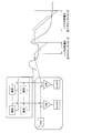
- FIG. 2 is an explanatory diagram showing timings that are susceptible to noise when digitizing a signal from a pixel.
- the signal from the pixel is digitized by controlling the counter at the timing at which the signal from the pixel and the slope of the output of the DAC (Digital Analog Converter) cross. At this time, the slope portion of the output of the DAC is a timing that is easily affected by noise.
- DAC Digital Analog Converter
- Evaluation of image noise is performed in a state where light with the most noticeable noise is blocked (light-shielded state). In the light-shielded state, the result is the same when reading the reference level and when reading the pixel level. If the switching between the HS section and the LP section of the MIPI occurs at the time of reading the reference level or the pixel level, the reading results do not become the same, and noise (a phenomenon that only a part of the image becomes bright or dark) occurs.
- This process is performed simultaneously for the pixel arrays on the same line, but the operation clock frequencies of the analog processing unit and the digital processing unit are the same, and switching between the HS section and the LP section of the MIPI is performed every several lines. In the case of occurrence of noise, generation of noise can be avoided by steadily delaying the output timing of the switching timing between the HS section and the LP section of the MIPI.
- the switching timing of the HS section and the LP section of MIPI shifts every moment.
- the respective operation clocks are asynchronous, and there are a plurality of types of phase relationships between the output signal of the DAC and the switching between the HS section and the LP section of the MIPI, and they change periodically. Therefore, it is not possible to suppress the generation of noise only by giving a steady delay to the switching timing between the HS section and the LP section, and the noise becomes periodically dark and light in the vertical direction.
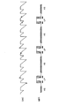
- FIG. 3A is an explanatory diagram showing a mechanism of noise generation due to switching between the HS section and the LP section of MIPI.
- FIG. 3B is an explanatory diagram showing an example of an image on which noise caused by switching between the HS section and the LP section of MIPI is superimposed. As shown in FIG. 3B, due to the switching between the HS section and the LP section of the MIPI, the noise appears as a periodic dark and light noise in the vertical direction.
- the present discloser has conducted intensive studies on a technique capable of suppressing the occurrence of image noise caused by switching between the HS section and the LP section in the MIPI standard.
- the present Disclosure has devised a technique capable of suppressing generation of image noise by controlling switching between the HS section and the LP section in the MIPI standard.
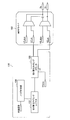
- FIG. 4 is an explanatory diagram illustrating a functional configuration example of the imaging device 100 according to the embodiment of the present disclosure.
- FIG. 4 is an explanatory diagram illustrating a functional configuration example of the imaging device 100 according to the embodiment of the present disclosure.
- an example of a functional configuration of the imaging device 100 according to the embodiment of the present disclosure will be described with reference to FIG.
- the imaging device 100 includes a pixel array 110, an analog processing unit 120, a storage unit 130, a signal processing unit 140, a control unit 150, an output process And a unit 160.
- the pixel array 110 is provided with pixels for photoelectrically converting incident light in an array, and outputs a pixel signal obtained by photoelectric conversion of incident light.
- the pixel signal from the pixel array 110 is sent to the analog processing unit 120.
- the analog processing unit 120 performs digitization processing on the pixel signal from the pixel array 110, which is an analog signal, and performs image processing on the digitized signal.
- the signal after performing the digitization and the image processing is sent to the storage unit 130.
- An output signal (for example, a horizontal synchronization signal) of a DAC used for digitization in the analog processing unit 120 is sent to the control unit 150.
- the storage unit 130 temporarily stores the signal output from the analog processing unit 120.
- the signal processing unit 140 reads out the signal stored in the storage unit 130 and performs a predetermined signal processing.
- the control unit 150 controls the switching timing of the HS section and the LP section of the output signal from the output processing unit 160 based on the DAC output signal from the analog processing unit 120 and the clock signal used in the signal processing unit 140. I do.
- the output processing unit 160 outputs a signal output from the signal processing unit 140 based on the control of the control unit 150.
- the control unit 150 controls the switching timing of the HS section and the LP section of the MIPI, so that the shading that has been generated periodically in the vertical direction becomes non-periodic in the entire screen. The noise changes to light and shade, making it difficult to see.
- FIG. 5 is an explanatory diagram showing an example of control of the switching timing of the HS section and the LP section of the MIPI by the control unit 150.
- the end of the HS section and the start time of the LP section, and the start time of the LP section and the start time of the HS section are changed for each frame and each horizontal cycle.
- the imaging apparatus 100 according to the embodiment of the present disclosure can operate in the vertical direction. By changing the shading that has occurred periodically to a non-periodic shading of the entire screen, it is possible to make the noise hard to be visually recognized.
- FIG. 6 is an explanatory diagram illustrating a first configuration example of the control unit 150 included in the imaging device 100 according to the embodiment of the present disclosure. Hereinafter, a configuration example of the control unit 150 will be described.
- the control unit 150 includes an M-sequence signal generation unit 151, a switching timing register 152, a timing generation unit 153, an addition unit 154, and a switching timing counter 155.
- FIG. 6 shows an example of the output processing unit 160 as a MIPI driver.
- the M-sequence signal generator 151 generates an M-sequence signal having a predetermined number of bits as a pseudo-random number. For example, when the M-sequence signal generation unit 151 generates a 7-bit M-sequence signal, 127 pieces of non-ordered data excluding zero are repeatedly generated. If the number of repetitions is small, periodic noise that does not have a sine wave shape is obtained. Therefore, it is desirable to have a certain word length.
- the output value cannot be directly used as the amplitude because there is a limit in the amplitude and fineness of the timing.
- the word length is long, only the necessary number of bits from the lower bits of the signal generated by M-sequence signal generation section 151 may be used. By using only the necessary number of bits from the lower bits of the signal, it is possible to select the number of bits required for the signal while securing the length of the repetition period to some extent.
- the switching timing register 152 stores a load value used for controlling switching timing between the HS section and the LP section. The load value stored in the switching timing register 152 is not changed.
- the timing generator 153 outputs a load (LD) signal to be supplied to the switching timing counter 155.
- LD load
- the addition unit 154 adds the signal generated by the M-sequence signal generation unit 151 and the load value held by the switching timing register 152, and outputs the result to the switching timing counter 155.
- the switching timing counter 155 controls switching timing between the HS section and the LP section in the output processing unit 160 based on the load (LD) signal.
- the load signal is also synchronized with the data in the HS section at a predetermined cycle. That is, the signal generated by the timing generation unit 153 and the horizontal synchronization signal HSync generated by the analog processing unit 120 are input to the switching timing counter 155.
- the switching timing counter 155 inputs a signal obtained by adding a signal generated by the M-sequence signal generation unit 151 that randomly changes to the load value held by the switching timing register 152, and switches between the HS section and the LP section. Control the timing. That is, in the first configuration example, the control unit 150 randomly changes the switching timing between the HS section and the LP section.
- control unit 150 By randomly changing the switching timing between the HS section and the LP section, the control unit 150 changes the shading that has occurred periodically in the vertical direction to the non-periodic shading of the entire screen, and the noise that is hardly visually recognized. It can be.
- the control unit 150 in the first configuration example can randomly change the switching timing between the HS section and the LP section, but the MIPI standard defines the minimum value of the switching time between the HS section and the LP section. . Therefore, the control unit 150 in the first configuration example randomly changes the switching timing between the HS section and the LP section so as not to fall below the minimum value of the switching time between the HS section and the LP section specified by the MIPI standard. Let it.
- control unit 150 controls to always shift the switching timing between the HS section and the LP section to a timing less affected by noise based on the horizontal synchronization signal generated by the analog processing unit 120. .
- FIG. 7 is an explanatory diagram showing how the switching timing between the HS section and the LP section is shifted to a timing less affected by noise.
- the switching timing between the HS section and the LP section is shifted not to the ramp portion of the output of the DAC but to a horizontal portion.
- FIG. 8 is an explanatory diagram illustrating a second configuration example of the control unit 150 included in the imaging device 100 according to the embodiment of the present disclosure. Hereinafter, a configuration example of the control unit 150 will be described.
- control unit 150 is configured to include the switching timing register 152 and the switching timing counter 155.
- FIG. 8 illustrates an example of the output processing unit 160 as an MIPI driver.
- the switching timing register 152 stores a load value used for controlling switching timing between the HS section and the LP section.
- the value stored in the switching timing register 152 can be changed according to the amount of noise.
- the amount of noise may be obtained by, for example, taking an average value of pixels for each line and obtaining variance.
- the variance differs greatly between periodic noise and noise that occurs randomly.
- a value that reduces the amount of noise is defined as a specified value. This allows the control unit 150 to shift the switching timing between the HS section and the LP section to a timing less affected by noise.
- the transfer rate in the HS section is a speed at which data in the HS section can be completely output before switching to the LP section.
- the control unit 150 sets the switching timing between the HS section and the LP section while referring to the ramp signal generated by the analog processing unit 120 so that the timing is less affected by noise.
- FIG. 9 is an explanatory diagram showing an example of the relationship between the ramp signal generated by the analog processing unit 120, the switching timing between the HS section and the LP section, and the noise amount.
- the switching timing between the HS section and the LP section is set to five as shown in FIG. 9, the pattern 3 has the largest noise amount and the pattern 1 has the smallest noise amount. Therefore, the control unit 150 according to the third configuration example sets the switching timing so that the HS section and the LP section are switched in pattern 1.
- FIG. 10 is an explanatory diagram illustrating a third configuration example of the control unit 150 included in the imaging device 100 according to the embodiment of the present disclosure. Hereinafter, a configuration example of the control unit 150 will be described.
- control unit 150 is configured to include the switching timing register 152, the switching timing counter 155, and the noise determination unit 156.
- FIG. 10 shows an example of the output processing unit 160 as a MIPI driver.
- the switching timing register 152 stores a load value used for controlling switching timing between the HS section and the LP section.
- the value stored in the switching timing register 152 can be changed according to the amount of noise.
- the noise amount may be obtained by, for example, taking an average value of pixels for each line and calculating variance.
- the variance differs greatly between periodic noise and noise that occurs randomly.
- a value that reduces the amount of noise is defined as a specified value. This allows the control unit 150 to shift the switching timing between the HS section and the LP section to a timing less affected by noise.
- the noise determination unit 156 determines the amount of noise in the image signal.
- the amount of noise has a correlation with the switching timing between the HS section and the LP section and the phase of the slope of the ramp signal. That is, when the value of the switching timing register 152 is sequentially increased or decreased, the noise amount increases or decreases according to the increase or decrease.
- the noise determination unit 156 can determine the setting that minimizes the noise by measuring the noise amount of the image signal for each setting of the switching timing register 152.
- the switching timing between the HS section and the LP section is restricted in the MIPI standard.
- the MIPI standard there is no definition of a maximum value for the switching time (THS-TRAIL) from the end of the HS section to the driving circuit for the LP and the time of the LP section. Therefore, when controlling the switching timing between the HS section and the LP section, the control unit 150 extends the switching time from the end of the HS section to the drive circuit for the LP and the time of the LP section while complying with the MIPI standard. . Thereby, the control unit 150 can change the switching timing between the HS section and the LP section without changing the transfer frequency.
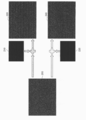
- FIG. 11 is an explanatory diagram for describing effects of the embodiment of the present disclosure.
- FIG. 11 shows a case where an image 210 having a noise of 64 ⁇ 3 (LSBrms) and a horizontal line of a sine wave having an amplitude of ⁇ 0.3 (LSB) are superimposed on an image 200, and an HS section according to the present embodiment.
- a case where the image 230 in which the switching timing of the LP section is changed is superimposed is shown.
- a sine wave horizontal streak having an amplitude of ⁇ 0.3 (LSB) is superimposed, horizontal stripe-like noise is conspicuous as in the image 220.
- the switching timing between the HS section and the LP section is changed. Then, the noise is less noticeable as in the image 240. That is, according to the present embodiment, it is possible to suppress the generation of image noise by controlling the switching between the HS section and the LP section in the MIPI standard.
- the imaging apparatus 100 that controls the end of the HS section and the start time of the LP section, and the start time of the LP section and the start time of the HS section. Can be done.
- the imaging apparatus 100 controls the end of the HS section and the start time of the LP section, and the start time of the LP section and the start time of the HS section, so that the By changing the generated shading to a non-periodic shading of the entire screen, it is possible to make the noise hard to be visually recognized.
- a computer program for causing hardware such as a CPU, ROM, and RAM incorporated in each device to exhibit the same function as the configuration of each device described above can also be created. Also, a storage medium storing the computer program can be provided. Further, by configuring each functional block shown in the functional block diagram by hardware, a series of processing can be realized by hardware.
- a conversion unit that converts an analog signal into a digital signal
- a signal processing unit that performs signal processing on the digital signal, A first data transmission mode of a communication mode of a data signal to be output, using at least a first signal used for conversion in the conversion unit and a second signal processed in the signal processing unit;
- a control unit that controls a timing of switching to a second data transmission mode having a lower transmission speed than the first data transmission mode based on a predetermined rule;
- An imaging device comprising: (2) The imaging device according to (1), wherein the control unit randomly changes a timing of switching between the first data transmission mode and the second data transmission mode as the predetermined rule.
- the imaging device according to (2) wherein the control unit randomly changes a timing of switching between the first data transmission mode and the second data transmission mode based on a pseudo-random number.
- the control unit changes timing of switching between the first data transmission mode and the second data transmission mode so as to avoid a predetermined period with reference to the first signal.
- the control unit measures a noise amount of the second signal, and changes a timing of switching between the first data transmission mode and the second data transmission mode at a timing when the noise amount is minimized.
- the imaging device according to (1) wherein the control unit randomly changes a timing of switching between the first data transmission mode and the second data transmission mode based on a pseudo-random number.
- the control unit changes timing of switching between the first data transmission mode and the second data transmission mode so as to avoid a predetermined period with reference to the first signal.
- the control unit may control the first data transmission in a range where a minimum value of a switching time between the first data transmission mode and the second data transmission mode does not fall below a minimum value defined in a rule of the communication mode.
- the communication mode is a mode conforming to a Mobile Industry Processor Interface (MIPI) standard.
- MIPI Mobile Industry Processor Interface
- (10) Converting an analog signal to a digital signal; performing signal processing on the digital signal; A first data transmission mode of a communication mode of a data signal to be output, using at least a first signal used for the conversion and a second signal processed in the signal processing; Controlling the timing of switching to the second data transmission mode having a lower transmission speed than the mode based on a predetermined rule;
- a control method comprising:
- imaging device 200 image 210 image 220 image 230 image 240 image
Landscapes
- Engineering & Computer Science (AREA)
- Multimedia (AREA)
- Signal Processing (AREA)
- Transforming Light Signals Into Electric Signals (AREA)
- Studio Devices (AREA)
Abstract
データ伝送モードの切り替わりのタイミングに起因する画像のノイズの発生を抑えることが可能な、撮像装置を提供する。アナログ信号をデジタル信号に変換する変換部(120)と、前記デジタル信号に対する信号処理を行う信号処理部(140)と、前記変換部での変換に用いる第1の信号と、前記信号処理部で処理される第2の信号とを少なくとも用いて、出力するデータ信号の通信モードの、第1のデータ伝送モードと、前記第1のデータ伝送モードよりも伝送速度が低速な第2のデータ伝送モードとに切り替わるタイミングを所定のルールに基づき制御する制御部(150)と、を備える、撮像装置(100)が提供される。
Description
本開示は、撮像装置及び制御方法に関する。
撮像装置の出力IFとしてMIPI(Mobile Industry Processor Interface)規格が多く使われている。MIPI規格で用いられるMIPI信号には、高速データ転送動作(HS)区間と、低消費電力動作(LP)区間が存在する。HS区間では小振幅差動信号で動作し、LP区間では電源からGNDまでの振幅を持つシングルエンド信号で動作する。MIPI規格に関する技術として例えば特許文献1などが開示されている。
HS区間とLP区間との切り替え時には、伝送路のレベル変動が発生し、変動に伴って伝送路を駆動する装置の電源やGNDの電流、電圧が変動する。このHS区間とLP区間との切り替えに伴い発生するGNDの変動が原因となり、撮像装置が生成する画像にノイズが発生する。
そこで、本開示では、データ伝送モードの切り替わりのタイミングを制御することでデータ伝送モードの切り替わりのタイミングに起因する画像のノイズの発生を抑えることが可能な、新規かつ改良された撮像装置及び制御方法を提案する。
本開示によれば、アナログ信号をデジタル信号に変換する変換部と、前記デジタル信号に対する信号処理を行う信号処理部と、前記変換部での変換に用いる第1の信号と、前記信号処理部で処理される第2の信号とを少なくとも用いて、出力するデータ信号の通信モードの、第1のデータ伝送モードと、前記第1のデータ伝送モードよりも伝送速度が低速な第2のデータ伝送モードとに切り替わるタイミングを所定のルールに基づき制御する制御部と、を備える、撮像装置が提供される。
本開示によれば、アナログ信号をデジタル信号に変換することと、前記デジタル信号に対する信号処理を行うことと、前記変換に用いる第1の信号と、前記信号処理で処理される第2の信号とを少なくとも用いて、出力するデータ信号の通信モードの、第1のデータ伝送モードと、前記第1のデータ伝送モードよりも伝送速度が低速な第2のデータ伝送モードとに切り替わるタイミングを所定のルールに基づき制御することと、を備える、制御方法が提供される。
以上説明したように本開示によれば、データ伝送モードの切り替わりのタイミングを制御することでデータ伝送モードの切り替わりのタイミングに起因する画像のノイズの発生を抑えることが可能な、新規かつ改良された撮像装置及び制御方法を提供することが出来る。
なお、上記の効果は必ずしも限定的なものではなく、上記の効果とともに、または上記の効果に代えて、本明細書に示されたいずれかの効果、または本明細書から把握され得る他の効果が奏されてもよい。
以下に添付図面を参照しながら、本開示の好適な実施の形態について詳細に説明する。なお、本明細書及び図面において、実質的に同一の機能構成を有する構成要素については、同一の符号を付することにより重複説明を省略する。
なお、説明は以下の順序で行うものとする。
1.本開示の実施の形態
1.1.経緯
1.2.構成例および動作例
2.まとめ
1.本開示の実施の形態
1.1.経緯
1.2.構成例および動作例
2.まとめ
<1.本開示の実施の形態>
[1.1.経緯]
本開示の実施の形態について詳細に説明する前に、本開示の実施の形態に至った経緯について説明する。
[1.1.経緯]
本開示の実施の形態について詳細に説明する前に、本開示の実施の形態に至った経緯について説明する。
撮像装置の出力IFとしてMIPI規格が多く使われている。MIPI規格で用いられるMIPI信号には、高速データ転送動作(HS)区間と、低消費電力動作(LP)区間が存在する。HS区間では小振幅差動信号で動作し、LP区間では電源からGNDまでの振幅を持つシングルエンド信号で動作する。図1は、HS区間の信号とLP区間の信号の例を示す説明図である。図1には、HS区間での250mVの振幅を有する作動信号と、LP区間でのGNDと1.2Vの電圧とで推移するシングルエンド信号とが示されている。
HS区間とLP区間との切り替え時には、伝送路のレベル変動が発生し、変動に伴って伝送路を駆動する装置の電源やGNDの電流、電圧が変動する。装置のGNDについては、アナログ処理部とデジタル処理部との間での干渉が少なくなるように工夫されるのが一般的ではある。しかし、撮像素子の基板を介してそれぞれのGNDが結合する等により、この干渉を完全に除くことはできない。このためMIPI信号の切り替え時に発生するGNDの変動が原因となり画像にノイズが発生する。
画素アレイの複数の画素のそれぞれから、入射光を光電変換して得られるアナログ画素信号とデジタル化の基準となる信号がアナログ処理部で比較され、その結果が一致するまでの時間をカウントしこれをデジタルの出力データとしている。この処理をしているタイミングが最もノイズの影響を受けやすい。図2は、画素からの信号をデジタル化する際の、ノイズの影響を受けやすいタイミングを示す説明図である。画素からの信号と、DAC(Digital Analog Convertor)の出力のスロープとがクロスするタイミングでカウンタを制御することで、画素からの信号がデジタル化される。この際、DACの出力のスロープ部分がノイズの影響を受けやすいタイミングである。
画像ノイズの評価は、ノイズが最も目立つ光を遮断した状態(遮光状態)で行われる。遮光状態の場合、基準レベルの読み込み時と画素レベルの読み取り時で結果が同じになる。この基準レベルまたは画素レベルの読み取り時にMIPIのHS区間とLP区間の切り替えが発生すると、それぞれの読み取り結果が同じにならず、ノイズ(画像の一部だけが明るくもしくは暗くなる現象)が発生する。
この処理は、同じライン上にある画素アレイについて同時に行われるが、アナログ処理部とデジタル処理部との動作クロックの周波数が同一で、かつMIPIのHS区間とLP区間の切り替えが数ライン毎に周期的に発生する場合は、MIPIのHS区間とLP区間の切り替えタイミングの出力されるタイミングを定常的に遅らせることによりノイズの発生を回避することができる。
しかし、アナログ処理部とデジタル処理部とで動作クロックの周波数が異なる場合、MIPIのHS区間とLP区間の切り替えタイミングが時々刻々とずれていく。それぞれの動作クロックは非同期であり、DACの出力信号と、MIPIのHS区間とLP区間の切り替えとの位相関係が複数通り存在し、かつ周期的に変化する。そのため、HS区間とLP区間の切り替えタイミングに定常的な遅延を与えるのみではノイズの発生を抑制することはできず、垂直方向に周期的な濃淡のノイズとなる。
図3Aは、MIPIのHS区間とLP区間の切り替えに起因するノイズの発生のメカニズムを示す説明図である。DACからの出力信号と、MIPIのHS区間とLP区間の切り替えタイミングの位相関係は複数通りあり、位相関係が周期的に変化する。従って、MIPIのHS区間とLP区間の切り替えタイミングが時々刻々とずれていく。
図3Bは、MIPIのHS区間とLP区間の切り替えに起因するノイズが乗った画像の例を示す説明図である。図3Bに示したように、MIPIのHS区間とLP区間の切り替えに起因して、垂直方向に周期的な濃淡のノイズとなって現れる。
そこで本件開示者は上述した点に鑑み、MIPI規格におけるHS区間とLP区間との切り替えに起因する画像のノイズの発生を抑えることが可能な技術について鋭意検討を行った。その結果、本件開示者は、以下で説明するように、MIPI規格におけるHS区間とLP区間との切り替えを制御することで画像のノイズの発生を抑えることが可能な技術を考案するに至った。
以上、本開示の実施の形態に至った経緯について説明した。
[1.2.構成例および動作例]
続いて、本開示の実施の形態に係る撮像装置の機能構成例を説明する。図4は、本開示の実施の形態に係る撮像装置100の機能構成例を示す説明図である。以下、図4を用いて本開示の実施の形態に係る撮像装置100の機能構成例について説明する。
続いて、本開示の実施の形態に係る撮像装置の機能構成例を説明する。図4は、本開示の実施の形態に係る撮像装置100の機能構成例を示す説明図である。以下、図4を用いて本開示の実施の形態に係る撮像装置100の機能構成例について説明する。
図4に示したように、本開示の実施の形態に係る撮像装置100は、画素アレイ110と、アナログ処理部120と、記憶部130と、信号処理部140と、制御部150と、出力処理部160と、を含んで構成される。
画素アレイ110は、入射光を光電変換する画素がアレイ状に設けられており、入射光の光電変換で得られる画素信号を出力する。画素アレイ110からの画素信号はアナログ処理部120に送られる。
アナログ処理部120は、アナログ信号である、画素アレイ110からの画素信号に対するデジタル化処理およびデジタル化後の信号に対する画像処理を実行する。デジタル化および画像処理を実行した後の信号は記憶部130送られる。また、アナログ処理部120でのデジタル化に用いられるDACの出力信号(例えば、水平同期信号)は制御部150に送られる。
記憶部130は、アナログ処理部120から出力される信号を一時的に記憶する。信号処理部140は、記憶部130に記憶された信号を読み出して所定の信号処理を実行する。
制御部150は、アナログ処理部120からのDACの出力信号と、信号処理部140で用いられるクロック信号とに基づき、出力処理部160からの出力信号の、HS区間とLP区間の切り替えタイミングを制御する。
出力処理部160は、信号処理部140から出力される信号を、制御部150の制御に基づいて出力する。出力処理部160からの出力信号について、制御部150がMIPIのHS区間とLP区間の切り替えタイミングを制御することで、縦方向に周期的に発生していた濃淡は、画面全体の非周期的な濃淡に変化し、視認されにくいノイズとなる。
図5は、制御部150によるMIPIのHS区間とLP区間の切り替えタイミングの制御例を示す説明図である。図5に示したように、HS区間の終了とLP区間の開始時間、および、LP区間の開始時間とHS区間の開始時間とを、フレーム毎および水平周期毎に変更する。このようにHS区間の終了とLP区間の開始時間、および、LP区間の開始時間とHS区間の開始時間とを制御することで、本開示の実施の形態に係る撮像装置100は、縦方向に周期的に発生していた濃淡を画面全体の非周期的な濃淡に変化させて、視認されにくいノイズとすることができる。
以上、図4を用いて本開示の実施の形態に係る撮像装置100の機能構成例について説明した。続いて、本開示の実施の形態に係る撮像装置100に含まれる制御部150の構成例について説明する。
(第1の構成例)
まず、制御部150の第1の構成例について説明する。図6は、本開示の実施の形態に係る撮像装置100に含まれる制御部150の第1の構成例を示す説明図である。以下、制御部150の構成例について説明する。
まず、制御部150の第1の構成例について説明する。図6は、本開示の実施の形態に係る撮像装置100に含まれる制御部150の第1の構成例を示す説明図である。以下、制御部150の構成例について説明する。
図6に示したように、制御部150は、M系列信号生成部151、切り替えタイミングレジスタ152、タイミング生成部153、加算部154、および切り替えタイミングカウンタ155を含んで構成される。また図6には出力処理部160の一例がMIPIドライバとして示されている。
M系列信号生成部151は、擬似ランダム数として、所定のビット数のM系列信号を生成する。例えばM系列信号生成部151が7ビットのM系列信号を生成する場合、ゼロを除く127個の順不同のデータを繰り返し生成する。繰返し回数が少ないと正弦波状ではない周期ノイズとなるため、ある程度の語長を有することが望ましい。
一方、語長が長すぎても、タイミングの振り幅と細かさに限度があるため、出力値をそのまま振り幅にすることはできない。語長が長い場合は、M系列信号生成部151が生成する信号の下位ビットから必要なビット数だけを利用しても良い。信号の下位ビットから必要なビット数だけを利用することで、繰り返し周期の長さをある程度確保しつつ、信号に必要なビット数の選択が可能となる。
切り替えタイミングレジスタ152は、HS区間とLP区間の切り替えタイミングの制御に用いるロード値を格納する。切り替えタイミングレジスタ152に格納されるロード値は変更されるものではない。
タイミング生成部153は、切り替えタイミングカウンタ155に供給するロード(LD)信号を出力する。
加算部154は、M系列信号生成部151が生成した信号と、切り替えタイミングレジスタ152が保持しているロード値とを加算し、切り替えタイミングカウンタ155に出力する。
切り替えタイミングカウンタ155は、ロード(LD)信号に基づいて、出力処理部160におけるHS区間とLP区間の切り替えタイミングを制御する。ロード信号は、所定の周期でHS区間のデータとも同期している。すなわち、切り替えタイミングカウンタ155には、タイミング生成部153が生成する信号と、アナログ処理部120で生成される水平同期信号HSyncと、が入力される。
そして切り替えタイミングカウンタ155は、切り替えタイミングレジスタ152が保持しているロード値に、ランダムに変化するM系列信号生成部151が生成した信号が加算された信号を入力し、HS区間とLP区間の切り替えタイミングを制御する。すなわち、第1の構成例では、制御部150は、HS区間とLP区間の切り替えタイミングをランダムに変化させる。
HS区間とLP区間の切り替えタイミングをランダムに変化させることで、制御部150は、縦方向に周期的に発生していた濃淡を画面全体の非周期的な濃淡に変化させて、視認されにくいノイズとすることができる。
第1の構成例における制御部150は、HS区間とLP区間の切り替えタイミングをランダムに変化させることができるが、MIPI規格においては、HS区間とLP区間の切り替え時間の最小値が定められている。従って、第1の構成例における制御部150は、MIPI規格で定められている、HS区間とLP区間の切り替え時間の最小値を下回らないように、HS区間とLP区間の切り替えタイミングをランダムに変化させる。
(第2の構成例)
続いて制御部150の第2の構成例について説明する。第2の構成例に係る制御部150は、HS区間とLP区間の切り替えタイミングを、アナログ処理部120で生成される水平同期信号に基づいて、ノイズの影響が少ないタイミングに常にシフトさせるよう制御する。
続いて制御部150の第2の構成例について説明する。第2の構成例に係る制御部150は、HS区間とLP区間の切り替えタイミングを、アナログ処理部120で生成される水平同期信号に基づいて、ノイズの影響が少ないタイミングに常にシフトさせるよう制御する。
図7は、HS区間とLP区間の切り替えタイミングを、ノイズの影響が少ないタイミングにシフトする様子を示す説明図である。図7には、HS区間とLP区間の切り替えタイミングを、DACの出力のランプ部分では無く、水平になっている部分にシフトさせている。このようにHS区間とLP区間の切り替えタイミングを制御することで、制御部150は、ノイズそのものを抑圧することができる。
図8は、本開示の実施の形態に係る撮像装置100に含まれる制御部150の第2の構成例を示す説明図である。以下、制御部150の構成例について説明する。
図8に示したように、制御部150は、切り替えタイミングレジスタ152および切り替えタイミングカウンタ155を含んで構成される。また図8には出力処理部160の一例がMIPIドライバとして示されている。
切り替えタイミングレジスタ152は、HS区間とLP区間の切り替えタイミングの制御に用いるロード値を格納する。この第2の構成例では、切り替えタイミングレジスタ152に格納される値は、ノイズ量に応じて変更されうる。ノイズ量は、例えば画素の1ライン毎の平均値をとり、分散を求めることで求められても良い。周期的なノイズと、ランダム的に発生するノイズでは、分散が大きく異なる。切り替えタイミングレジスタ152に格納される値は、ノイズ量が少なくなる値を規定値とする。これにより、制御部150は、HS区間とLP区間の切り替えタイミングを、ノイズの影響が少ないタイミングにシフトさせることができる。
この第2の構成例では、HS区間のデータとは無関係にLP区間への切り替えを行う。従って、HS区間の転送レートは、LP区間に切り替わる前に、HS区間のデータを出しきることが出来る程度の速度である。
(第3の構成例)
続いて制御部150の第3の構成例について説明する。第3の構成例に係る制御部150は、アナログ処理部120で生成されるランプ信号を参照しながら、ノイズの影響が少ないタイミングとなるように、HS区間とLP区間の切り替えタイミングを設定する。
続いて制御部150の第3の構成例について説明する。第3の構成例に係る制御部150は、アナログ処理部120で生成されるランプ信号を参照しながら、ノイズの影響が少ないタイミングとなるように、HS区間とLP区間の切り替えタイミングを設定する。
図9は、アナログ処理部120で生成されるランプ信号とHS区間とLP区間の切り替えタイミングとノイズ量の関係例を示す説明図である。HS区間とLP区間の切り替えタイミングを、図9のように5通りに設定した場合、最もノイズ量が大きいのはパターン3であり、最もノイズ量が少ないのはパターン1である。従って第3の構成例に係る制御部150は、パターン1でHS区間とLP区間とが切り替わるように切り替えタイミングを設定する。
図10は、本開示の実施の形態に係る撮像装置100に含まれる制御部150の第3の構成例を示す説明図である。以下、制御部150の構成例について説明する。
図10に示したように、制御部150は、切り替えタイミングレジスタ152、切り替えタイミングカウンタ155およびノイズ判定部156を含んで構成される。また図10には出力処理部160の一例がMIPIドライバとして示されている。
切り替えタイミングレジスタ152は、HS区間とLP区間の切り替えタイミングの制御に用いるロード値を格納する。この第3の構成例では、切り替えタイミングレジスタ152に格納される値は、ノイズ量に応じて変更されうる。ノイズ量は、例えば画素の1ライン毎の平均値をとり、分散を求めることで求められても良い。周期的なノイズと、ランダム的に発生するノイズでは、分散が大きく異なる。切り替えタイミングレジスタ152に格納される値は、ノイズ量が少なくなる値を規定値とする。これにより、制御部150は、HS区間とLP区間の切り替えタイミングを、ノイズの影響が少ないタイミングにシフトさせることができる。
ノイズ判定部156は、画像信号におけるノイズ量の判定を行う。ノイズ量は、HS区間とLP区間の切り替えタイミングと、ランプ信号の傾きとの位相に相関がある。すなわち、切り替えタイミングレジスタ152の値を順次増加、または減少させると、増加または減少に応じてノイズ量も増減する。ノイズ判定部156は、切り替えタイミングレジスタ152の設定毎の、画像信号のノイズ量を測定することで、ノイズが最小となる設定を判定することが出来る。
上述したように、MIPI規格においては、HS区間とLP区間の切り替えタイミングに制約がある。一方、MIPI規格においては、HS区間の終了からLP用の駆動回路への切り替え時間(THS-TRAIL)、および、LP区間の時間については最大値の規定は存在しない。従って、制御部150は、HS区間とLP区間の切り替えタイミングの制御に際し、MIPI規格を準拠しつつ、HS区間の終了からLP用の駆動回路への切り替え時間、および、LP区間の時間を伸長させる。これにより、制御部150は、転送周波数を変えること無く、HS区間とLP区間の切り替えタイミングを変化させることができる。
最後に、本開示の実施の形態による効果について説明する。図11は、本開示の実施の形態の効果を説明するための説明図である。
図11には、ノイズが64±3(LSBrms)の画像200に、振幅が±0.3(LSB)の正弦波の横筋が乗った画像210を重畳した場合と、本実施形態によりHS区間とLP区間の切り替えタイミングを変化させた画像230を重畳した場合とが示されている。振幅が±0.3(LSB)の正弦波の横筋を重畳すると、画像220のように横縞状のノイズが目立ってしまうのに対し、本実施形態によりHS区間とLP区間の切り替えタイミングを変化させると、画像240のようにノイズが目立たなくなっている。すなわち、本実施形態により、MIPI規格におけるHS区間とLP区間との切り替えを制御することで画像のノイズの発生を抑えることが可能となっている。
<2.まとめ>
以上説明したように本開示の実施の形態によれば、HS区間の終了とLP区間の開始時間、および、LP区間の開始時間とHS区間の開始時間とを制御する撮像装置100を提供することが出来る。本開示の実施の形態に係る撮像装置100は、HS区間の終了とLP区間の開始時間、および、LP区間の開始時間とHS区間の開始時間とを制御することで、縦方向に周期的に発生していた濃淡を画面全体の非周期的な濃淡に変化させて、視認されにくいノイズとすることができる。
以上説明したように本開示の実施の形態によれば、HS区間の終了とLP区間の開始時間、および、LP区間の開始時間とHS区間の開始時間とを制御する撮像装置100を提供することが出来る。本開示の実施の形態に係る撮像装置100は、HS区間の終了とLP区間の開始時間、および、LP区間の開始時間とHS区間の開始時間とを制御することで、縦方向に周期的に発生していた濃淡を画面全体の非周期的な濃淡に変化させて、視認されにくいノイズとすることができる。
各装置に内蔵されるCPU、ROMおよびRAMなどのハードウェアを、上述した各装置の構成と同等の機能を発揮させるためのコンピュータプログラムも作成可能である。また、該コンピュータプログラムを記憶させた記憶媒体も提供されることが可能である。また、機能ブロック図で示したそれぞれの機能ブロックをハードウェアで構成することで、一連の処理をハードウェアで実現することもできる。
以上、添付図面を参照しながら本開示の好適な実施形態について詳細に説明したが、本開示の技術的範囲はかかる例に限定されない。本開示の技術分野における通常の知識を有する者であれば、請求の範囲に記載された技術的思想の範疇内において、各種の変更例または修正例に想到し得ることは明らかであり、これらについても、当然に本開示の技術的範囲に属するものと了解される。
また、本明細書に記載された効果は、あくまで説明的または例示的なものであって限定的ではない。つまり、本開示に係る技術は、上記の効果とともに、または上記の効果に代えて、本明細書の記載から当業者には明らかな他の効果を奏しうる。
なお、以下のような構成も本開示の技術的範囲に属する。
(1)
アナログ信号をデジタル信号に変換する変換部と、
前記デジタル信号に対する信号処理を行う信号処理部と、
前記変換部での変換に用いる第1の信号と、前記信号処理部で処理される第2の信号とを少なくとも用いて、出力するデータ信号の通信モードの、第1のデータ伝送モードと、前記第1のデータ伝送モードよりも伝送速度が低速な第2のデータ伝送モードとに切り替わるタイミングを所定のルールに基づき制御する制御部と、
を備える、撮像装置。
(2)
前記制御部は、前記所定のルールとして前記第1のデータ伝送モードと前記第2のデータ伝送モードとの切り替わりのタイミングをランダムに変化させる、前記(1)に記載の撮像装置。
(3)
前記制御部は、擬似ランダム数に基づいて前記第1のデータ伝送モードと前記第2のデータ伝送モードとの切り替わりのタイミングをランダムに変化させる、前記(2)に記載の撮像装置。
(4)
前記制御部は、前記第1の信号を参照して所定の期間を避けるように、前記第1のデータ伝送モードと前記第2のデータ伝送モードとの切り替わりのタイミングを変化させる、前記(1)に記載の撮像装置。
(5)
前記第1の信号は、ランプ信号である、前記(4)に記載の撮像装置。
(6)
前記制御部は、前記第2の信号のノイズ量を測定し、該ノイズ量が最小となるタイミングで前記第1のデータ伝送モードと前記第2のデータ伝送モードとの切り替わりのタイミングを変化させる、前記(1)に記載の撮像装置。
(7)
前記制御部は、前記第1のデータ伝送モードと前記第2のデータ伝送モードとの切り替え時間の最小値が前記通信モードの規則に定められた最小値を下回らない範囲で前記第1のデータ伝送モードと前記第2のデータ伝送モードとの切り替わりのタイミングを制御する、前記(1)~(6)のいずれかに記載の撮像装置。
(8)
前記アナログ信号を生成する画素がアレイ状に配列された画素アレイをさらに備える、前記(1)~(7)のいずれかに記載の撮像装置。
(9)
前記通信モードは、MIPI(Mobile Industry Processor Interface)規格に準拠するモードである、前記(1)~(8)のいずれかに記載の撮像装置。
(10)
アナログ信号をデジタル信号に変換することと、 前記デジタル信号に対する信号処理を行うことと、
前記変換に用いる第1の信号と、前記信号処理で処理される第2の信号とを少なくとも用いて、出力するデータ信号の通信モードの、第1のデータ伝送モードと、前記第1のデータ伝送モードよりも伝送速度が低速な第2のデータ伝送モードとに切り替わるタイミングを所定のルールに基づき制御することと、
を備える、制御方法。
(1)
アナログ信号をデジタル信号に変換する変換部と、
前記デジタル信号に対する信号処理を行う信号処理部と、
前記変換部での変換に用いる第1の信号と、前記信号処理部で処理される第2の信号とを少なくとも用いて、出力するデータ信号の通信モードの、第1のデータ伝送モードと、前記第1のデータ伝送モードよりも伝送速度が低速な第2のデータ伝送モードとに切り替わるタイミングを所定のルールに基づき制御する制御部と、
を備える、撮像装置。
(2)
前記制御部は、前記所定のルールとして前記第1のデータ伝送モードと前記第2のデータ伝送モードとの切り替わりのタイミングをランダムに変化させる、前記(1)に記載の撮像装置。
(3)
前記制御部は、擬似ランダム数に基づいて前記第1のデータ伝送モードと前記第2のデータ伝送モードとの切り替わりのタイミングをランダムに変化させる、前記(2)に記載の撮像装置。
(4)
前記制御部は、前記第1の信号を参照して所定の期間を避けるように、前記第1のデータ伝送モードと前記第2のデータ伝送モードとの切り替わりのタイミングを変化させる、前記(1)に記載の撮像装置。
(5)
前記第1の信号は、ランプ信号である、前記(4)に記載の撮像装置。
(6)
前記制御部は、前記第2の信号のノイズ量を測定し、該ノイズ量が最小となるタイミングで前記第1のデータ伝送モードと前記第2のデータ伝送モードとの切り替わりのタイミングを変化させる、前記(1)に記載の撮像装置。
(7)
前記制御部は、前記第1のデータ伝送モードと前記第2のデータ伝送モードとの切り替え時間の最小値が前記通信モードの規則に定められた最小値を下回らない範囲で前記第1のデータ伝送モードと前記第2のデータ伝送モードとの切り替わりのタイミングを制御する、前記(1)~(6)のいずれかに記載の撮像装置。
(8)
前記アナログ信号を生成する画素がアレイ状に配列された画素アレイをさらに備える、前記(1)~(7)のいずれかに記載の撮像装置。
(9)
前記通信モードは、MIPI(Mobile Industry Processor Interface)規格に準拠するモードである、前記(1)~(8)のいずれかに記載の撮像装置。
(10)
アナログ信号をデジタル信号に変換することと、 前記デジタル信号に対する信号処理を行うことと、
前記変換に用いる第1の信号と、前記信号処理で処理される第2の信号とを少なくとも用いて、出力するデータ信号の通信モードの、第1のデータ伝送モードと、前記第1のデータ伝送モードよりも伝送速度が低速な第2のデータ伝送モードとに切り替わるタイミングを所定のルールに基づき制御することと、
を備える、制御方法。
100 撮像装置
200 画像
210 画像
220 画像
230 画像
240 画像
200 画像
210 画像
220 画像
230 画像
240 画像
Claims (10)
- アナログ信号をデジタル信号に変換する変換部と、
前記デジタル信号に対する信号処理を行う信号処理部と、
前記変換部での変換に用いる第1の信号と、前記信号処理部で処理される第2の信号とを少なくとも用いて、出力するデータ信号の通信モードの、第1のデータ伝送モードと、前記第1のデータ伝送モードよりも伝送速度が低速な第2のデータ伝送モードとに切り替わるタイミングを所定のルールに基づき制御する制御部と、
を備える、撮像装置。 - 前記制御部は、前記所定のルールとして前記第1のデータ伝送モードと前記第2のデータ伝送モードとの切り替わりのタイミングをランダムに変化させる、請求項1に記載の撮像装置。
- 前記制御部は、擬似ランダム数に基づいて前記第1のデータ伝送モードと前記第2のデータ伝送モードとの切り替わりのタイミングをランダムに変化させる、請求項2に記載の撮像装置。
- 前記制御部は、前記第1の信号を参照して所定の期間を避けるように、前記第1のデータ伝送モードと前記第2のデータ伝送モードとの切り替わりのタイミングを変化させる、請求項1に記載の撮像装置。
- 前記第1の信号は、ランプ信号である、請求項4に記載の撮像装置。
- 前記制御部は、前記第2の信号のノイズ量を測定し、該ノイズ量が最小となるタイミングで前記第1のデータ伝送モードと前記第2のデータ伝送モードとの切り替わりのタイミングを変化させる、請求項1に記載の撮像装置。
- 前記制御部は、前記第1のデータ伝送モードと前記第2のデータ伝送モードとの切り替え時間の最小値が前記通信モードの規則に定められた最小値を下回らない範囲で前記第1のデータ伝送モードと前記第2のデータ伝送モードとの切り替わりのタイミングを制御する、請求項1に記載の撮像装置。
- 前記アナログ信号を生成する画素がアレイ状に配列された画素アレイをさらに備える、請求項1に記載の撮像装置。
- 前記通信モードは、MIPI(Mobile Industry Processor Interface)規格に準拠するモードである、請求項1に記載の撮像装置。
- アナログ信号をデジタル信号に変換することと、
前記デジタル信号に対する信号処理を行うことと、
前記変換に用いる第1の信号と、前記信号処理で処理される第2の信号とを少なくとも用いて、出力するデータ信号の通信モードの、第1のデータ伝送モードと、前記第1のデータ伝送モードよりも伝送速度が低速な第2のデータ伝送モードとに切り替わるタイミングを所定のルールに基づき制御することと、
を備える、制御方法。
Applications Claiming Priority (2)
| Application Number | Priority Date | Filing Date | Title |
|---|---|---|---|
| JP2018-150673 | 2018-08-09 | ||
| JP2018150673A JP2020027978A (ja) | 2018-08-09 | 2018-08-09 | 撮像装置及び制御方法 |
Publications (1)
| Publication Number | Publication Date |
|---|---|
| WO2020031560A1 true WO2020031560A1 (ja) | 2020-02-13 |
Family
ID=69414730
Family Applications (1)
| Application Number | Title | Priority Date | Filing Date |
|---|---|---|---|
| PCT/JP2019/026363 Ceased WO2020031560A1 (ja) | 2018-08-09 | 2019-07-02 | 撮像装置及び制御方法 |
Country Status (2)
| Country | Link |
|---|---|
| JP (1) | JP2020027978A (ja) |
| WO (1) | WO2020031560A1 (ja) |
Citations (3)
| Publication number | Priority date | Publication date | Assignee | Title |
|---|---|---|---|---|
| JP2015177364A (ja) * | 2014-03-14 | 2015-10-05 | シナプティクス・ディスプレイ・デバイス合同会社 | レシーバ回路、表示パネルドライバ、表示装置及びレシーバ回路の動作方法 |
| JP2017112427A (ja) * | 2015-12-14 | 2017-06-22 | シナプティクス・ジャパン合同会社 | 受信回路、表示ドライバ及び表示装置 |
| JP2017195500A (ja) * | 2016-04-20 | 2017-10-26 | ソニー株式会社 | 受信装置、送信装置、および通信システム、ならびに、信号受信方法、信号送信方法、および通信方法 |
-
2018
- 2018-08-09 JP JP2018150673A patent/JP2020027978A/ja active Pending
-
2019
- 2019-07-02 WO PCT/JP2019/026363 patent/WO2020031560A1/ja not_active Ceased
Patent Citations (3)
| Publication number | Priority date | Publication date | Assignee | Title |
|---|---|---|---|---|
| JP2015177364A (ja) * | 2014-03-14 | 2015-10-05 | シナプティクス・ディスプレイ・デバイス合同会社 | レシーバ回路、表示パネルドライバ、表示装置及びレシーバ回路の動作方法 |
| JP2017112427A (ja) * | 2015-12-14 | 2017-06-22 | シナプティクス・ジャパン合同会社 | 受信回路、表示ドライバ及び表示装置 |
| JP2017195500A (ja) * | 2016-04-20 | 2017-10-26 | ソニー株式会社 | 受信装置、送信装置、および通信システム、ならびに、信号受信方法、信号送信方法、および通信方法 |
Also Published As
| Publication number | Publication date |
|---|---|
| JP2020027978A (ja) | 2020-02-20 |
Similar Documents
| Publication | Publication Date | Title |
|---|---|---|
| US7292170B2 (en) | System and method for improved time-interleaved analog-to-digital converter arrays | |
| JP4455513B2 (ja) | 画像処理方法、画像処理装置、及び画像表示装置 | |
| CN101674432A (zh) | 多信道采样系统及方法 | |
| WO1999055078A1 (en) | False contour correcting apparatus and method | |
| KR20190044261A (ko) | 저잡음 싱글-슬롭 비교 장치 및 그에 따른 아날로그-디지털 변환 장치와 씨모스 이미지 센서 | |
| US20140055583A1 (en) | Endoscope system | |
| US7049994B2 (en) | Semiconductor integrated circuit | |
| WO2020031560A1 (ja) | 撮像装置及び制御方法 | |
| JPH08228280A (ja) | イメージセンサの画像信号処理装置 | |
| JP5677919B2 (ja) | ランプ波生成回路および固体撮像装置 | |
| US10263631B2 (en) | Analog digital converter | |
| JP2010220148A (ja) | コード生成回路およびイメージセンサ | |
| JP5410454B2 (ja) | パルスパターン発生装置及び該装置を用いた誤り率測定システム並びにパルスパターン発生方法 | |
| JP2008232857A (ja) | 波形発生器および試験装置 | |
| JP2004128637A (ja) | D/aコンバータ | |
| JP5245665B2 (ja) | データ受信回路 | |
| JP7668773B2 (ja) | 信号発生装置及びそれを用いたエンファシス切り替え方法 | |
| KR20070024208A (ko) | 비디오 신호 처리 장치 및 방법 | |
| JP2015133631A (ja) | アナログデジタル変換装置 | |
| JP5617449B2 (ja) | 画像読取装置 | |
| US20240395222A1 (en) | Data communication system, and display device | |
| JP2009164726A (ja) | 駆動信号生成装置及び画像読取装置 | |
| WO2023157487A1 (ja) | クロック制御回路、および撮像素子 | |
| JP2974318B2 (ja) | 画像処理装置 | |
| JP2005252703A (ja) | アナログ/ディジタル変換回路及びそれを内蔵した半導体集積回路 |
Legal Events
| Date | Code | Title | Description |
|---|---|---|---|
| 121 | Ep: the epo has been informed by wipo that ep was designated in this application |
Ref document number: 19846144 Country of ref document: EP Kind code of ref document: A1 |
|
| NENP | Non-entry into the national phase |
Ref country code: DE |
|
| 122 | Ep: pct application non-entry in european phase |
Ref document number: 19846144 Country of ref document: EP Kind code of ref document: A1 |