WO2020026851A1 - Élément d'imagerie et dispositif d'imagerie - Google Patents
Élément d'imagerie et dispositif d'imagerie Download PDFInfo
- Publication number
- WO2020026851A1 WO2020026851A1 PCT/JP2019/028474 JP2019028474W WO2020026851A1 WO 2020026851 A1 WO2020026851 A1 WO 2020026851A1 JP 2019028474 W JP2019028474 W JP 2019028474W WO 2020026851 A1 WO2020026851 A1 WO 2020026851A1
- Authority
- WO
- WIPO (PCT)
- Prior art keywords
- layer
- electrode
- photoelectric conversion
- unit
- hydrogen
- Prior art date
Links
- 238000003384 imaging method Methods 0.000 title claims abstract description 202
- 238000006243 chemical reaction Methods 0.000 claims abstract description 215
- 239000001257 hydrogen Substances 0.000 claims abstract description 114
- 229910052739 hydrogen Inorganic materials 0.000 claims abstract description 114
- 239000004065 semiconductor Substances 0.000 claims abstract description 112
- UFHFLCQGNIYNRP-UHFFFAOYSA-N Hydrogen Chemical compound [H][H] UFHFLCQGNIYNRP-UHFFFAOYSA-N 0.000 claims abstract description 103
- 239000000758 substrate Substances 0.000 claims abstract description 74
- 230000000903 blocking effect Effects 0.000 claims abstract description 40
- 239000010410 layer Substances 0.000 claims description 406
- 238000003860 storage Methods 0.000 claims description 123
- 239000011241 protective layer Substances 0.000 claims description 59
- 230000002093 peripheral effect Effects 0.000 claims description 31
- LIVNPJMFVYWSIS-UHFFFAOYSA-N silicon monoxide Chemical compound [Si-]#[O+] LIVNPJMFVYWSIS-UHFFFAOYSA-N 0.000 claims description 18
- VYPSYNLAJGMNEJ-UHFFFAOYSA-N Silicium dioxide Chemical compound O=[Si]=O VYPSYNLAJGMNEJ-UHFFFAOYSA-N 0.000 claims description 17
- 229910052814 silicon oxide Inorganic materials 0.000 claims description 17
- TWNQGVIAIRXVLR-UHFFFAOYSA-N oxo(oxoalumanyloxy)alumane Chemical compound O=[Al]O[Al]=O TWNQGVIAIRXVLR-UHFFFAOYSA-N 0.000 claims description 16
- 229910052581 Si3N4 Inorganic materials 0.000 claims description 14
- HQVNEWCFYHHQES-UHFFFAOYSA-N silicon nitride Chemical compound N12[Si]34N5[Si]62N3[Si]51N64 HQVNEWCFYHHQES-UHFFFAOYSA-N 0.000 claims description 14
- 239000002356 single layer Substances 0.000 claims description 13
- XUIMIQQOPSSXEZ-UHFFFAOYSA-N Silicon Chemical compound [Si] XUIMIQQOPSSXEZ-UHFFFAOYSA-N 0.000 claims description 12
- 229910052710 silicon Inorganic materials 0.000 claims description 12
- 239000010703 silicon Substances 0.000 claims description 12
- OKTJSMMVPCPJKN-UHFFFAOYSA-N Carbon Chemical compound [C] OKTJSMMVPCPJKN-UHFFFAOYSA-N 0.000 claims description 11
- 229910052799 carbon Inorganic materials 0.000 claims description 9
- 239000011810 insulating material Substances 0.000 claims description 7
- 229910044991 metal oxide Inorganic materials 0.000 claims description 7
- 150000004706 metal oxides Chemical class 0.000 claims description 7
- 239000000463 material Substances 0.000 description 59
- 238000000034 method Methods 0.000 description 47
- 238000009792 diffusion process Methods 0.000 description 41
- 238000007667 floating Methods 0.000 description 41
- 238000012545 processing Methods 0.000 description 40
- 238000004891 communication Methods 0.000 description 27
- 238000001514 detection method Methods 0.000 description 24
- 230000006870 function Effects 0.000 description 21
- 238000005516 engineering process Methods 0.000 description 20
- 239000011229 interlayer Substances 0.000 description 20
- 238000010586 diagram Methods 0.000 description 18
- 238000012546 transfer Methods 0.000 description 18
- 230000003287 optical effect Effects 0.000 description 16
- 230000008569 process Effects 0.000 description 16
- 239000002775 capsule Substances 0.000 description 15
- 238000001727 in vivo Methods 0.000 description 15
- 230000004048 modification Effects 0.000 description 13
- 238000012986 modification Methods 0.000 description 13
- 239000000975 dye Substances 0.000 description 12
- 150000002431 hydrogen Chemical class 0.000 description 11
- 238000002674 endoscopic surgery Methods 0.000 description 10
- 238000000231 atomic layer deposition Methods 0.000 description 9
- 230000005540 biological transmission Effects 0.000 description 9
- 239000011368 organic material Substances 0.000 description 9
- 238000005240 physical vapour deposition Methods 0.000 description 9
- 238000005229 chemical vapour deposition Methods 0.000 description 8
- 230000000149 penetrating effect Effects 0.000 description 8
- 210000001519 tissue Anatomy 0.000 description 8
- XLOMVQKBTHCTTD-UHFFFAOYSA-N Zinc monoxide Chemical compound [Zn]=O XLOMVQKBTHCTTD-UHFFFAOYSA-N 0.000 description 7
- 238000009825 accumulation Methods 0.000 description 7
- 229920002120 photoresistant polymer Polymers 0.000 description 6
- BBEAQIROQSPTKN-UHFFFAOYSA-N pyrene Chemical compound C1=CC=C2C=CC3=CC=CC4=CC=C1C2=C43 BBEAQIROQSPTKN-UHFFFAOYSA-N 0.000 description 6
- GVEPBJHOBDJJJI-UHFFFAOYSA-N fluoranthrene Natural products C1=CC(C2=CC=CC=C22)=C3C2=CC=CC3=C1 GVEPBJHOBDJJJI-UHFFFAOYSA-N 0.000 description 5
- 230000007246 mechanism Effects 0.000 description 5
- 238000007789 sealing Methods 0.000 description 5
- 238000004544 sputter deposition Methods 0.000 description 5
- XLYOFNOQVPJJNP-UHFFFAOYSA-N water Substances O XLYOFNOQVPJJNP-UHFFFAOYSA-N 0.000 description 5
- MWPLVEDNUUSJAV-UHFFFAOYSA-N anthracene Chemical compound C1=CC=CC2=CC3=CC=CC=C3C=C21 MWPLVEDNUUSJAV-UHFFFAOYSA-N 0.000 description 4
- QVGXLLKOCUKJST-UHFFFAOYSA-N atomic oxygen Chemical compound [O] QVGXLLKOCUKJST-UHFFFAOYSA-N 0.000 description 4
- 230000008859 change Effects 0.000 description 4
- 230000005284 excitation Effects 0.000 description 4
- 239000001301 oxygen Substances 0.000 description 4
- 229910052760 oxygen Inorganic materials 0.000 description 4
- 238000001356 surgical procedure Methods 0.000 description 4
- 229910052782 aluminium Inorganic materials 0.000 description 3
- XAGFODPZIPBFFR-UHFFFAOYSA-N aluminium Chemical compound [Al] XAGFODPZIPBFFR-UHFFFAOYSA-N 0.000 description 3
- 230000006866 deterioration Effects 0.000 description 3
- 239000002019 doping agent Substances 0.000 description 3
- 230000000694 effects Effects 0.000 description 3
- 238000010336 energy treatment Methods 0.000 description 3
- 238000004519 manufacturing process Methods 0.000 description 3
- 239000000434 metal complex dye Substances 0.000 description 3
- 238000002156 mixing Methods 0.000 description 3
- -1 polycyclic hydrocarbon compound Chemical class 0.000 description 3
- 238000007639 printing Methods 0.000 description 3
- 230000006798 recombination Effects 0.000 description 3
- 238000005215 recombination Methods 0.000 description 3
- 239000010936 titanium Substances 0.000 description 3
- 239000011787 zinc oxide Substances 0.000 description 3
- UJOBWOGCFQCDNV-UHFFFAOYSA-N 9H-carbazole Chemical compound C1=CC=C2C3=CC=CC=C3NC2=C1 UJOBWOGCFQCDNV-UHFFFAOYSA-N 0.000 description 2
- GYHNNYVSQQEPJS-UHFFFAOYSA-N Gallium Chemical compound [Ga] GYHNNYVSQQEPJS-UHFFFAOYSA-N 0.000 description 2
- SIKJAQJRHWYJAI-UHFFFAOYSA-N Indole Chemical compound C1=CC=C2NC=CC2=C1 SIKJAQJRHWYJAI-UHFFFAOYSA-N 0.000 description 2
- UFWIBTONFRDIAS-UHFFFAOYSA-N Naphthalene Chemical compound C1=CC=CC2=CC=CC=C21 UFWIBTONFRDIAS-UHFFFAOYSA-N 0.000 description 2
- KAESVJOAVNADME-UHFFFAOYSA-N Pyrrole Chemical compound C=1C=CNC=1 KAESVJOAVNADME-UHFFFAOYSA-N 0.000 description 2
- SMWDFEZZVXVKRB-UHFFFAOYSA-N Quinoline Chemical compound N1=CC=CC2=CC=CC=C21 SMWDFEZZVXVKRB-UHFFFAOYSA-N 0.000 description 2
- BOTDANWDWHJENH-UHFFFAOYSA-N Tetraethyl orthosilicate Chemical compound CCO[Si](OCC)(OCC)OCC BOTDANWDWHJENH-UHFFFAOYSA-N 0.000 description 2
- YTPLMLYBLZKORZ-UHFFFAOYSA-N Thiophene Chemical compound C=1C=CSC=1 YTPLMLYBLZKORZ-UHFFFAOYSA-N 0.000 description 2
- NRTOMJZYCJJWKI-UHFFFAOYSA-N Titanium nitride Chemical compound [Ti]#N NRTOMJZYCJJWKI-UHFFFAOYSA-N 0.000 description 2
- 230000009471 action Effects 0.000 description 2
- CUFNKYGDVFVPHO-UHFFFAOYSA-N azulene Chemical compound C1=CC=CC2=CC=CC2=C1 CUFNKYGDVFVPHO-UHFFFAOYSA-N 0.000 description 2
- IOJUPLGTWVMSFF-UHFFFAOYSA-N benzothiazole Chemical compound C1=CC=C2SC=NC2=C1 IOJUPLGTWVMSFF-UHFFFAOYSA-N 0.000 description 2
- 230000015572 biosynthetic process Effects 0.000 description 2
- 210000004204 blood vessel Anatomy 0.000 description 2
- 239000003153 chemical reaction reagent Substances 0.000 description 2
- 230000000295 complement effect Effects 0.000 description 2
- 239000000470 constituent Substances 0.000 description 2
- 230000007547 defect Effects 0.000 description 2
- 238000011161 development Methods 0.000 description 2
- 230000018109 developmental process Effects 0.000 description 2
- JAONJTDQXUSBGG-UHFFFAOYSA-N dialuminum;dizinc;oxygen(2-) Chemical compound [O-2].[O-2].[O-2].[O-2].[O-2].[Al+3].[Al+3].[Zn+2].[Zn+2] JAONJTDQXUSBGG-UHFFFAOYSA-N 0.000 description 2
- 238000001312 dry etching Methods 0.000 description 2
- 238000010894 electron beam technology Methods 0.000 description 2
- 238000005530 etching Methods 0.000 description 2
- 229910001938 gadolinium oxide Inorganic materials 0.000 description 2
- 229940075613 gadolinium oxide Drugs 0.000 description 2
- CMIHHWBVHJVIGI-UHFFFAOYSA-N gadolinium(iii) oxide Chemical compound [O-2].[O-2].[O-2].[Gd+3].[Gd+3] CMIHHWBVHJVIGI-UHFFFAOYSA-N 0.000 description 2
- 229910052733 gallium Inorganic materials 0.000 description 2
- 150000002391 heterocyclic compounds Chemical class 0.000 description 2
- AMGQUBHHOARCQH-UHFFFAOYSA-N indium;oxotin Chemical compound [In].[Sn]=O AMGQUBHHOARCQH-UHFFFAOYSA-N 0.000 description 2
- MOFVSTNWEDAEEK-UHFFFAOYSA-M indocyanine green Chemical compound [Na+].[O-]S(=O)(=O)CCCCN1C2=CC=C3C=CC=CC3=C2C(C)(C)C1=CC=CC=CC=CC1=[N+](CCCCS([O-])(=O)=O)C2=CC=C(C=CC=C3)C3=C2C1(C)C MOFVSTNWEDAEEK-UHFFFAOYSA-M 0.000 description 2
- 229960004657 indocyanine green Drugs 0.000 description 2
- 238000009434 installation Methods 0.000 description 2
- 238000005468 ion implantation Methods 0.000 description 2
- 230000001678 irradiating effect Effects 0.000 description 2
- MRELNEQAGSRDBK-UHFFFAOYSA-N lanthanum(3+);oxygen(2-) Chemical compound [O-2].[O-2].[O-2].[La+3].[La+3] MRELNEQAGSRDBK-UHFFFAOYSA-N 0.000 description 2
- 229910052751 metal Inorganic materials 0.000 description 2
- 239000002184 metal Substances 0.000 description 2
- PLDDOISOJJCEMH-UHFFFAOYSA-N neodymium(3+);oxygen(2-) Chemical compound [O-2].[O-2].[O-2].[Nd+3].[Nd+3] PLDDOISOJJCEMH-UHFFFAOYSA-N 0.000 description 2
- 210000000056 organ Anatomy 0.000 description 2
- 239000012044 organic layer Substances 0.000 description 2
- YNPNZTXNASCQKK-UHFFFAOYSA-N phenanthrene Chemical compound C1=CC=C2C3=CC=CC=C3C=CC2=C1 YNPNZTXNASCQKK-UHFFFAOYSA-N 0.000 description 2
- ZIKATJAYWZUJPY-UHFFFAOYSA-N thulium(iii) oxide Chemical compound [O-2].[O-2].[O-2].[Tm+3].[Tm+3] ZIKATJAYWZUJPY-UHFFFAOYSA-N 0.000 description 2
- 229910052719 titanium Inorganic materials 0.000 description 2
- OGIDPMRJRNCKJF-UHFFFAOYSA-N titanium oxide Inorganic materials [Ti]=O OGIDPMRJRNCKJF-UHFFFAOYSA-N 0.000 description 2
- 238000002834 transmittance Methods 0.000 description 2
- 229910052721 tungsten Inorganic materials 0.000 description 2
- QGKMIGUHVLGJBR-UHFFFAOYSA-M (4z)-1-(3-methylbutyl)-4-[[1-(3-methylbutyl)quinolin-1-ium-4-yl]methylidene]quinoline;iodide Chemical compound [I-].C12=CC=CC=C2N(CCC(C)C)C=CC1=CC1=CC=[N+](CCC(C)C)C2=CC=CC=C12 QGKMIGUHVLGJBR-UHFFFAOYSA-M 0.000 description 1
- BCMCBBGGLRIHSE-UHFFFAOYSA-N 1,3-benzoxazole Chemical compound C1=CC=C2OC=NC2=C1 BCMCBBGGLRIHSE-UHFFFAOYSA-N 0.000 description 1
- AIQCTYVNRWYDIF-UHFFFAOYSA-N 1-phenyl-9h-xanthene Chemical compound C=12CC3=CC=CC=C3OC2=CC=CC=1C1=CC=CC=C1 AIQCTYVNRWYDIF-UHFFFAOYSA-N 0.000 description 1
- BSKHPKMHTQYZBB-UHFFFAOYSA-N 2-methylpyridine Chemical compound CC1=CC=CC=N1 BSKHPKMHTQYZBB-UHFFFAOYSA-N 0.000 description 1
- XMWRBQBLMFGWIX-UHFFFAOYSA-N C60 fullerene Chemical compound C12=C3C(C4=C56)=C7C8=C5C5=C9C%10=C6C6=C4C1=C1C4=C6C6=C%10C%10=C9C9=C%11C5=C8C5=C8C7=C3C3=C7C2=C1C1=C2C4=C6C4=C%10C6=C9C9=C%11C5=C5C8=C3C3=C7C1=C1C2=C4C6=C2C9=C5C3=C12 XMWRBQBLMFGWIX-UHFFFAOYSA-N 0.000 description 1
- 229930192627 Naphthoquinone Natural products 0.000 description 1
- NRCMAYZCPIVABH-UHFFFAOYSA-N Quinacridone Chemical compound N1C2=CC=CC=C2C(=O)C2=C1C=C1C(=O)C3=CC=CC=C3NC1=C2 NRCMAYZCPIVABH-UHFFFAOYSA-N 0.000 description 1
- 239000012327 Ruthenium complex Substances 0.000 description 1
- 229910006404 SnO 2 Inorganic materials 0.000 description 1
- XBDYBAVJXHJMNQ-UHFFFAOYSA-N Tetrahydroanthracene Natural products C1=CC=C2C=C(CCCC3)C3=CC2=C1 XBDYBAVJXHJMNQ-UHFFFAOYSA-N 0.000 description 1
- GWEVSGVZZGPLCZ-UHFFFAOYSA-N Titan oxide Chemical compound O=[Ti]=O GWEVSGVZZGPLCZ-UHFFFAOYSA-N 0.000 description 1
- RTAQQCXQSZGOHL-UHFFFAOYSA-N Titanium Chemical compound [Ti] RTAQQCXQSZGOHL-UHFFFAOYSA-N 0.000 description 1
- 229910003363 ZnMgO Inorganic materials 0.000 description 1
- 229910007717 ZnSnO Inorganic materials 0.000 description 1
- RWBMMASKJODNSV-UHFFFAOYSA-N [1]benzothiolo[2,3-g][1]benzothiole Chemical compound C1=CC=C2C3=C(SC=C4)C4=CC=C3SC2=C1 RWBMMASKJODNSV-UHFFFAOYSA-N 0.000 description 1
- UPEMFLOMQVFMCZ-UHFFFAOYSA-N [O--].[O--].[O--].[Pm+3].[Pm+3] Chemical compound [O--].[O--].[O--].[Pm+3].[Pm+3] UPEMFLOMQVFMCZ-UHFFFAOYSA-N 0.000 description 1
- 238000010521 absorption reaction Methods 0.000 description 1
- 230000001133 acceleration Effects 0.000 description 1
- HSFWRNGVRCDJHI-UHFFFAOYSA-N alpha-acetylene Natural products C#C HSFWRNGVRCDJHI-UHFFFAOYSA-N 0.000 description 1
- 238000000137 annealing Methods 0.000 description 1
- 239000001000 anthraquinone dye Substances 0.000 description 1
- 150000001491 aromatic compounds Chemical class 0.000 description 1
- 230000008901 benefit Effects 0.000 description 1
- 230000000740 bleeding effect Effects 0.000 description 1
- 150000001638 boron Chemical class 0.000 description 1
- LLCSWKVOHICRDD-UHFFFAOYSA-N buta-1,3-diyne Chemical group C#CC#C LLCSWKVOHICRDD-UHFFFAOYSA-N 0.000 description 1
- 238000004364 calculation method Methods 0.000 description 1
- 239000002041 carbon nanotube Substances 0.000 description 1
- 229910021393 carbon nanotube Inorganic materials 0.000 description 1
- 229910000420 cerium oxide Inorganic materials 0.000 description 1
- 238000000701 chemical imaging Methods 0.000 description 1
- 239000011248 coating agent Substances 0.000 description 1
- 238000000576 coating method Methods 0.000 description 1
- 239000003086 colorant Substances 0.000 description 1
- 238000002485 combustion reaction Methods 0.000 description 1
- 239000002131 composite material Substances 0.000 description 1
- 150000001875 compounds Chemical class 0.000 description 1
- 238000010276 construction Methods 0.000 description 1
- PMHQVHHXPFUNSP-UHFFFAOYSA-M copper(1+);methylsulfanylmethane;bromide Chemical compound Br[Cu].CSC PMHQVHHXPFUNSP-UHFFFAOYSA-M 0.000 description 1
- 238000012937 correction Methods 0.000 description 1
- 230000000779 depleting effect Effects 0.000 description 1
- 238000000151 deposition Methods 0.000 description 1
- 230000008021 deposition Effects 0.000 description 1
- 238000013461 design Methods 0.000 description 1
- 229910003460 diamond Inorganic materials 0.000 description 1
- 239000010432 diamond Substances 0.000 description 1
- 238000010494 dissociation reaction Methods 0.000 description 1
- 230000005593 dissociations Effects 0.000 description 1
- 238000009826 distribution Methods 0.000 description 1
- 150000004662 dithiols Chemical class 0.000 description 1
- 229910003440 dysprosium oxide Inorganic materials 0.000 description 1
- NLQFUUYNQFMIJW-UHFFFAOYSA-N dysprosium(iii) oxide Chemical compound O=[Dy]O[Dy]=O NLQFUUYNQFMIJW-UHFFFAOYSA-N 0.000 description 1
- 230000005684 electric field Effects 0.000 description 1
- 125000002534 ethynyl group Chemical group [H]C#C* 0.000 description 1
- 229910001940 europium oxide Inorganic materials 0.000 description 1
- AEBZCFFCDTZXHP-UHFFFAOYSA-N europium(3+);oxygen(2-) Chemical compound [O-2].[O-2].[O-2].[Eu+3].[Eu+3] AEBZCFFCDTZXHP-UHFFFAOYSA-N 0.000 description 1
- 238000001704 evaporation Methods 0.000 description 1
- 230000029142 excretion Effects 0.000 description 1
- 238000002073 fluorescence micrograph Methods 0.000 description 1
- 229910003472 fullerene Inorganic materials 0.000 description 1
- 230000004313 glare Effects 0.000 description 1
- 229910021389 graphene Inorganic materials 0.000 description 1
- 229910052735 hafnium Inorganic materials 0.000 description 1
- 229910000449 hafnium oxide Inorganic materials 0.000 description 1
- WIHZLLGSGQNAGK-UHFFFAOYSA-N hafnium(4+);oxygen(2-) Chemical compound [O-2].[O-2].[Hf+4] WIHZLLGSGQNAGK-UHFFFAOYSA-N 0.000 description 1
- 230000005525 hole transport Effects 0.000 description 1
- JYTUFVYWTIKZGR-UHFFFAOYSA-N holmium oxide Inorganic materials [O][Ho]O[Ho][O] JYTUFVYWTIKZGR-UHFFFAOYSA-N 0.000 description 1
- OWCYYNSBGXMRQN-UHFFFAOYSA-N holmium(3+);oxygen(2-) Chemical compound [O-2].[O-2].[O-2].[Ho+3].[Ho+3] OWCYYNSBGXMRQN-UHFFFAOYSA-N 0.000 description 1
- 230000006872 improvement Effects 0.000 description 1
- 239000012535 impurity Substances 0.000 description 1
- 229910052738 indium Inorganic materials 0.000 description 1
- APFVFJFRJDLVQX-UHFFFAOYSA-N indium atom Chemical compound [In] APFVFJFRJDLVQX-UHFFFAOYSA-N 0.000 description 1
- PZOUSPYUWWUPPK-UHFFFAOYSA-N indole Natural products CC1=CC=CC2=C1C=CN2 PZOUSPYUWWUPPK-UHFFFAOYSA-N 0.000 description 1
- RKJUIXBNRJVNHR-UHFFFAOYSA-N indolenine Natural products C1=CC=C2CC=NC2=C1 RKJUIXBNRJVNHR-UHFFFAOYSA-N 0.000 description 1
- 239000012212 insulator Substances 0.000 description 1
- 230000010354 integration Effects 0.000 description 1
- 210000000936 intestine Anatomy 0.000 description 1
- 230000031700 light absorption Effects 0.000 description 1
- 238000001459 lithography Methods 0.000 description 1
- 229910003443 lutetium oxide Inorganic materials 0.000 description 1
- 238000001755 magnetron sputter deposition Methods 0.000 description 1
- 239000011159 matrix material Substances 0.000 description 1
- 238000005259 measurement Methods 0.000 description 1
- DZVCFNFOPIZQKX-LTHRDKTGSA-M merocyanine Chemical compound [Na+].O=C1N(CCCC)C(=O)N(CCCC)C(=O)C1=C\C=C\C=C/1N(CCCS([O-])(=O)=O)C2=CC=CC=C2O\1 DZVCFNFOPIZQKX-LTHRDKTGSA-M 0.000 description 1
- 125000001434 methanylylidene group Chemical group [H]C#[*] 0.000 description 1
- 239000003595 mist Substances 0.000 description 1
- 230000000116 mitigating effect Effects 0.000 description 1
- 210000004400 mucous membrane Anatomy 0.000 description 1
- 150000002791 naphthoquinones Chemical class 0.000 description 1
- IJGRMHOSHXDMSA-UHFFFAOYSA-N nitrogen Substances N#N IJGRMHOSHXDMSA-UHFFFAOYSA-N 0.000 description 1
- 229910052757 nitrogen Inorganic materials 0.000 description 1
- 239000013307 optical fiber Substances 0.000 description 1
- 230000001151 other effect Effects 0.000 description 1
- BMMGVYCKOGBVEV-UHFFFAOYSA-N oxo(oxoceriooxy)cerium Chemical compound [Ce]=O.O=[Ce]=O BMMGVYCKOGBVEV-UHFFFAOYSA-N 0.000 description 1
- MPARYNQUYZOBJM-UHFFFAOYSA-N oxo(oxolutetiooxy)lutetium Chemical compound O=[Lu]O[Lu]=O MPARYNQUYZOBJM-UHFFFAOYSA-N 0.000 description 1
- SIWVEOZUMHYXCS-UHFFFAOYSA-N oxo(oxoyttriooxy)yttrium Chemical compound O=[Y]O[Y]=O SIWVEOZUMHYXCS-UHFFFAOYSA-N 0.000 description 1
- MMKQUGHLEMYQSG-UHFFFAOYSA-N oxygen(2-);praseodymium(3+) Chemical compound [O-2].[O-2].[O-2].[Pr+3].[Pr+3] MMKQUGHLEMYQSG-UHFFFAOYSA-N 0.000 description 1
- BPUBBGLMJRNUCC-UHFFFAOYSA-N oxygen(2-);tantalum(5+) Chemical compound [O-2].[O-2].[O-2].[O-2].[O-2].[Ta+5].[Ta+5] BPUBBGLMJRNUCC-UHFFFAOYSA-N 0.000 description 1
- UZLYXNNZYFBAQO-UHFFFAOYSA-N oxygen(2-);ytterbium(3+) Chemical compound [O-2].[O-2].[O-2].[Yb+3].[Yb+3] UZLYXNNZYFBAQO-UHFFFAOYSA-N 0.000 description 1
- RVTZCBVAJQQJTK-UHFFFAOYSA-N oxygen(2-);zirconium(4+) Chemical compound [O-2].[O-2].[Zr+4] RVTZCBVAJQQJTK-UHFFFAOYSA-N 0.000 description 1
- 238000000059 patterning Methods 0.000 description 1
- 230000035515 penetration Effects 0.000 description 1
- SLIUAWYAILUBJU-UHFFFAOYSA-N pentacene Chemical compound C1=CC=CC2=CC3=CC4=CC5=CC=CC=C5C=C4C=C3C=C21 SLIUAWYAILUBJU-UHFFFAOYSA-N 0.000 description 1
- 230000008855 peristalsis Effects 0.000 description 1
- 125000002080 perylenyl group Chemical group C1(=CC=C2C=CC=C3C4=CC=CC5=CC=CC(C1=C23)=C45)* 0.000 description 1
- CSHWQDPOILHKBI-UHFFFAOYSA-N peryrene Natural products C1=CC(C2=CC=CC=3C2=C2C=CC=3)=C3C2=CC=CC3=C1 CSHWQDPOILHKBI-UHFFFAOYSA-N 0.000 description 1
- 239000001007 phthalocyanine dye Substances 0.000 description 1
- 238000005498 polishing Methods 0.000 description 1
- 229920000642 polymer Polymers 0.000 description 1
- 150000004032 porphyrins Chemical class 0.000 description 1
- 229910003447 praseodymium oxide Inorganic materials 0.000 description 1
- 230000009467 reduction Effects 0.000 description 1
- 230000008929 regeneration Effects 0.000 description 1
- 238000011069 regeneration method Methods 0.000 description 1
- 229910001954 samarium oxide Inorganic materials 0.000 description 1
- 229940075630 samarium oxide Drugs 0.000 description 1
- FKTOIHSPIPYAPE-UHFFFAOYSA-N samarium(iii) oxide Chemical compound [O-2].[O-2].[O-2].[Sm+3].[Sm+3] FKTOIHSPIPYAPE-UHFFFAOYSA-N 0.000 description 1
- 238000000926 separation method Methods 0.000 description 1
- HBMJWWWQQXIZIP-UHFFFAOYSA-N silicon carbide Chemical compound [Si+]#[C-] HBMJWWWQQXIZIP-UHFFFAOYSA-N 0.000 description 1
- 229910010271 silicon carbide Inorganic materials 0.000 description 1
- 230000005236 sound signal Effects 0.000 description 1
- 230000003595 spectral effect Effects 0.000 description 1
- 238000004528 spin coating Methods 0.000 description 1
- 230000002269 spontaneous effect Effects 0.000 description 1
- 210000002784 stomach Anatomy 0.000 description 1
- PMJMHCXAGMRGBZ-UHFFFAOYSA-N subphthalocyanine Chemical compound N1C(N=C2C3=CC=CC=C3C(=N3)N2)=C(C=CC=C2)C2=C1N=C1C2=CC=CC=C2C3=N1 PMJMHCXAGMRGBZ-UHFFFAOYSA-N 0.000 description 1
- 230000003746 surface roughness Effects 0.000 description 1
- 229910001936 tantalum oxide Inorganic materials 0.000 description 1
- 230000002123 temporal effect Effects 0.000 description 1
- 229910003451 terbium oxide Inorganic materials 0.000 description 1
- SCRZPWWVSXWCMC-UHFFFAOYSA-N terbium(iii) oxide Chemical compound [O-2].[O-2].[O-2].[Tb+3].[Tb+3] SCRZPWWVSXWCMC-UHFFFAOYSA-N 0.000 description 1
- IFLREYGFSNHWGE-UHFFFAOYSA-N tetracene Chemical compound C1=CC=CC2=CC3=CC4=CC=CC=C4C=C3C=C21 IFLREYGFSNHWGE-UHFFFAOYSA-N 0.000 description 1
- 229930192474 thiophene Natural products 0.000 description 1
- XOLBLPGZBRYERU-UHFFFAOYSA-N tin dioxide Chemical compound O=[Sn]=O XOLBLPGZBRYERU-UHFFFAOYSA-N 0.000 description 1
- 229910001887 tin oxide Inorganic materials 0.000 description 1
- 229910052723 transition metal Inorganic materials 0.000 description 1
- 150000003624 transition metals Chemical class 0.000 description 1
- AAAQKTZKLRYKHR-UHFFFAOYSA-N triphenylmethane Chemical compound C1=CC=CC=C1C(C=1C=CC=CC=1)C1=CC=CC=C1 AAAQKTZKLRYKHR-UHFFFAOYSA-N 0.000 description 1
- WFKWXMTUELFFGS-UHFFFAOYSA-N tungsten Chemical compound [W] WFKWXMTUELFFGS-UHFFFAOYSA-N 0.000 description 1
- 239000010937 tungsten Substances 0.000 description 1
- 238000001771 vacuum deposition Methods 0.000 description 1
- 230000000007 visual effect Effects 0.000 description 1
- 239000001018 xanthene dye Substances 0.000 description 1
- 229910003454 ytterbium oxide Inorganic materials 0.000 description 1
- 229940075624 ytterbium oxide Drugs 0.000 description 1
- YVTHLONGBIQYBO-UHFFFAOYSA-N zinc indium(3+) oxygen(2-) Chemical compound [O--].[Zn++].[In+3] YVTHLONGBIQYBO-UHFFFAOYSA-N 0.000 description 1
- 229910001928 zirconium oxide Inorganic materials 0.000 description 1
Images


Classifications
-
- H—ELECTRICITY
- H01—ELECTRIC ELEMENTS
- H01L—SEMICONDUCTOR DEVICES NOT COVERED BY CLASS H10
- H01L27/00—Devices consisting of a plurality of semiconductor or other solid-state components formed in or on a common substrate
- H01L27/14—Devices consisting of a plurality of semiconductor or other solid-state components formed in or on a common substrate including semiconductor components sensitive to infrared radiation, light, electromagnetic radiation of shorter wavelength or corpuscular radiation and specially adapted either for the conversion of the energy of such radiation into electrical energy or for the control of electrical energy by such radiation
- H01L27/144—Devices controlled by radiation
- H01L27/146—Imager structures
- H01L27/14665—Imagers using a photoconductor layer
-
- H—ELECTRICITY
- H01—ELECTRIC ELEMENTS
- H01L—SEMICONDUCTOR DEVICES NOT COVERED BY CLASS H10
- H01L27/00—Devices consisting of a plurality of semiconductor or other solid-state components formed in or on a common substrate
- H01L27/14—Devices consisting of a plurality of semiconductor or other solid-state components formed in or on a common substrate including semiconductor components sensitive to infrared radiation, light, electromagnetic radiation of shorter wavelength or corpuscular radiation and specially adapted either for the conversion of the energy of such radiation into electrical energy or for the control of electrical energy by such radiation
- H01L27/144—Devices controlled by radiation
- H01L27/146—Imager structures
- H01L27/14601—Structural or functional details thereof
- H01L27/14609—Pixel-elements with integrated switching, control, storage or amplification elements
- H01L27/1461—Pixel-elements with integrated switching, control, storage or amplification elements characterised by the photosensitive area
-
- H—ELECTRICITY
- H01—ELECTRIC ELEMENTS
- H01L—SEMICONDUCTOR DEVICES NOT COVERED BY CLASS H10
- H01L27/00—Devices consisting of a plurality of semiconductor or other solid-state components formed in or on a common substrate
- H01L27/14—Devices consisting of a plurality of semiconductor or other solid-state components formed in or on a common substrate including semiconductor components sensitive to infrared radiation, light, electromagnetic radiation of shorter wavelength or corpuscular radiation and specially adapted either for the conversion of the energy of such radiation into electrical energy or for the control of electrical energy by such radiation
- H01L27/144—Devices controlled by radiation
- H01L27/146—Imager structures
- H01L27/14601—Structural or functional details thereof
- H01L27/1462—Coatings
- H01L27/14621—Colour filter arrangements
-
- H—ELECTRICITY
- H01—ELECTRIC ELEMENTS
- H01L—SEMICONDUCTOR DEVICES NOT COVERED BY CLASS H10
- H01L27/00—Devices consisting of a plurality of semiconductor or other solid-state components formed in or on a common substrate
- H01L27/14—Devices consisting of a plurality of semiconductor or other solid-state components formed in or on a common substrate including semiconductor components sensitive to infrared radiation, light, electromagnetic radiation of shorter wavelength or corpuscular radiation and specially adapted either for the conversion of the energy of such radiation into electrical energy or for the control of electrical energy by such radiation
- H01L27/144—Devices controlled by radiation
- H01L27/146—Imager structures
- H01L27/14601—Structural or functional details thereof
- H01L27/14638—Structures specially adapted for transferring the charges across the imager perpendicular to the imaging plane
-
- H—ELECTRICITY
- H01—ELECTRIC ELEMENTS
- H01L—SEMICONDUCTOR DEVICES NOT COVERED BY CLASS H10
- H01L27/00—Devices consisting of a plurality of semiconductor or other solid-state components formed in or on a common substrate
- H01L27/14—Devices consisting of a plurality of semiconductor or other solid-state components formed in or on a common substrate including semiconductor components sensitive to infrared radiation, light, electromagnetic radiation of shorter wavelength or corpuscular radiation and specially adapted either for the conversion of the energy of such radiation into electrical energy or for the control of electrical energy by such radiation
- H01L27/144—Devices controlled by radiation
- H01L27/146—Imager structures
- H01L27/14643—Photodiode arrays; MOS imagers
- H01L27/14645—Colour imagers
- H01L27/14647—Multicolour imagers having a stacked pixel-element structure, e.g. npn, npnpn or MQW elements
-
- H—ELECTRICITY
- H04—ELECTRIC COMMUNICATION TECHNIQUE
- H04N—PICTORIAL COMMUNICATION, e.g. TELEVISION
- H04N25/00—Circuitry of solid-state image sensors [SSIS]; Control thereof
- H04N25/70—SSIS architectures; Circuits associated therewith
- H04N25/76—Addressed sensors, e.g. MOS or CMOS sensors
-
- H—ELECTRICITY
- H10—SEMICONDUCTOR DEVICES; ELECTRIC SOLID-STATE DEVICES NOT OTHERWISE PROVIDED FOR
- H10K—ORGANIC ELECTRIC SOLID-STATE DEVICES
- H10K30/00—Organic devices sensitive to infrared radiation, light, electromagnetic radiation of shorter wavelength or corpuscular radiation
- H10K30/80—Constructional details
- H10K30/81—Electrodes
- H10K30/82—Transparent electrodes, e.g. indium tin oxide [ITO] electrodes
-
- H—ELECTRICITY
- H10—SEMICONDUCTOR DEVICES; ELECTRIC SOLID-STATE DEVICES NOT OTHERWISE PROVIDED FOR
- H10K—ORGANIC ELECTRIC SOLID-STATE DEVICES
- H10K39/00—Integrated devices, or assemblies of multiple devices, comprising at least one organic radiation-sensitive element covered by group H10K30/00
- H10K39/30—Devices controlled by radiation
- H10K39/32—Organic image sensors
-
- H—ELECTRICITY
- H01—ELECTRIC ELEMENTS
- H01L—SEMICONDUCTOR DEVICES NOT COVERED BY CLASS H10
- H01L27/00—Devices consisting of a plurality of semiconductor or other solid-state components formed in or on a common substrate
- H01L27/14—Devices consisting of a plurality of semiconductor or other solid-state components formed in or on a common substrate including semiconductor components sensitive to infrared radiation, light, electromagnetic radiation of shorter wavelength or corpuscular radiation and specially adapted either for the conversion of the energy of such radiation into electrical energy or for the control of electrical energy by such radiation
- H01L27/144—Devices controlled by radiation
- H01L27/146—Imager structures
- H01L27/14601—Structural or functional details thereof
- H01L27/14603—Special geometry or disposition of pixel-elements, address-lines or gate-electrodes
- H01L27/14607—Geometry of the photosensitive area
-
- H—ELECTRICITY
- H01—ELECTRIC ELEMENTS
- H01L—SEMICONDUCTOR DEVICES NOT COVERED BY CLASS H10
- H01L27/00—Devices consisting of a plurality of semiconductor or other solid-state components formed in or on a common substrate
- H01L27/14—Devices consisting of a plurality of semiconductor or other solid-state components formed in or on a common substrate including semiconductor components sensitive to infrared radiation, light, electromagnetic radiation of shorter wavelength or corpuscular radiation and specially adapted either for the conversion of the energy of such radiation into electrical energy or for the control of electrical energy by such radiation
- H01L27/144—Devices controlled by radiation
- H01L27/146—Imager structures
- H01L27/14601—Structural or functional details thereof
- H01L27/1462—Coatings
- H01L27/14623—Optical shielding
-
- H—ELECTRICITY
- H01—ELECTRIC ELEMENTS
- H01L—SEMICONDUCTOR DEVICES NOT COVERED BY CLASS H10
- H01L27/00—Devices consisting of a plurality of semiconductor or other solid-state components formed in or on a common substrate
- H01L27/14—Devices consisting of a plurality of semiconductor or other solid-state components formed in or on a common substrate including semiconductor components sensitive to infrared radiation, light, electromagnetic radiation of shorter wavelength or corpuscular radiation and specially adapted either for the conversion of the energy of such radiation into electrical energy or for the control of electrical energy by such radiation
- H01L27/144—Devices controlled by radiation
- H01L27/146—Imager structures
- H01L27/14601—Structural or functional details thereof
- H01L27/14625—Optical elements or arrangements associated with the device
- H01L27/14627—Microlenses
-
- H—ELECTRICITY
- H01—ELECTRIC ELEMENTS
- H01L—SEMICONDUCTOR DEVICES NOT COVERED BY CLASS H10
- H01L27/00—Devices consisting of a plurality of semiconductor or other solid-state components formed in or on a common substrate
- H01L27/14—Devices consisting of a plurality of semiconductor or other solid-state components formed in or on a common substrate including semiconductor components sensitive to infrared radiation, light, electromagnetic radiation of shorter wavelength or corpuscular radiation and specially adapted either for the conversion of the energy of such radiation into electrical energy or for the control of electrical energy by such radiation
- H01L27/144—Devices controlled by radiation
- H01L27/146—Imager structures
- H01L27/14601—Structural or functional details thereof
- H01L27/1464—Back illuminated imager structures
-
- H—ELECTRICITY
- H01—ELECTRIC ELEMENTS
- H01L—SEMICONDUCTOR DEVICES NOT COVERED BY CLASS H10
- H01L27/00—Devices consisting of a plurality of semiconductor or other solid-state components formed in or on a common substrate
- H01L27/14—Devices consisting of a plurality of semiconductor or other solid-state components formed in or on a common substrate including semiconductor components sensitive to infrared radiation, light, electromagnetic radiation of shorter wavelength or corpuscular radiation and specially adapted either for the conversion of the energy of such radiation into electrical energy or for the control of electrical energy by such radiation
- H01L27/144—Devices controlled by radiation
- H01L27/146—Imager structures
- H01L27/14601—Structural or functional details thereof
- H01L27/14641—Electronic components shared by two or more pixel-elements, e.g. one amplifier shared by two pixel elements
-
- Y—GENERAL TAGGING OF NEW TECHNOLOGICAL DEVELOPMENTS; GENERAL TAGGING OF CROSS-SECTIONAL TECHNOLOGIES SPANNING OVER SEVERAL SECTIONS OF THE IPC; TECHNICAL SUBJECTS COVERED BY FORMER USPC CROSS-REFERENCE ART COLLECTIONS [XRACs] AND DIGESTS
- Y02—TECHNOLOGIES OR APPLICATIONS FOR MITIGATION OR ADAPTATION AGAINST CLIMATE CHANGE
- Y02E—REDUCTION OF GREENHOUSE GAS [GHG] EMISSIONS, RELATED TO ENERGY GENERATION, TRANSMISSION OR DISTRIBUTION
- Y02E10/00—Energy generation through renewable energy sources
- Y02E10/50—Photovoltaic [PV] energy
- Y02E10/549—Organic PV cells
-
- Y—GENERAL TAGGING OF NEW TECHNOLOGICAL DEVELOPMENTS; GENERAL TAGGING OF CROSS-SECTIONAL TECHNOLOGIES SPANNING OVER SEVERAL SECTIONS OF THE IPC; TECHNICAL SUBJECTS COVERED BY FORMER USPC CROSS-REFERENCE ART COLLECTIONS [XRACs] AND DIGESTS
- Y02—TECHNOLOGIES OR APPLICATIONS FOR MITIGATION OR ADAPTATION AGAINST CLIMATE CHANGE
- Y02P—CLIMATE CHANGE MITIGATION TECHNOLOGIES IN THE PRODUCTION OR PROCESSING OF GOODS
- Y02P70/00—Climate change mitigation technologies in the production process for final industrial or consumer products
- Y02P70/50—Manufacturing or production processes characterised by the final manufactured product
Definitions
- the present disclosure relates to an imaging device and an imaging device having a photoelectric conversion layer using an organic semiconductor material.
- an imaging device such as a CCD (Charge Coupled Device) image sensor or a CMOS (Complementary Metal Oxide Semiconductor) image sensor
- an organic photoelectric conversion layer using an organic semiconductor material is formed on a semiconductor substrate having a buried photodiode.
- a so-called stacked type imaging device that is stacked is used.
- the stacked-type imaging device has an advantage that a signal of R / G / B can be extracted from one pixel, and no demosaicing is required, so that a false color does not occur.
- the charge generated by photoelectric conversion is temporarily stored in the inorganic photoelectric conversion unit and then transferred to a floating diffusion layer (floating diffusion; FD). It can be completely depleted.
- the organic photoelectric conversion unit having the organic photoelectric conversion layer the charge generated by the photoelectric conversion is directly accumulated in the floating diffusion layer FD, so that it is difficult to completely deplete the organic photoelectric conversion unit.
- the kTC noise increases, the random noise worsens, and the image quality deteriorates.
- Patent Literature 1 in a photoelectric conversion unit provided above a semiconductor substrate and formed by stacking a first electrode, a photoelectric conversion layer, and a second electrode, the photoelectric conversion unit is disposed separately from the first electrode.
- an image pickup device having a charge storage electrode disposed to face a photoelectric conversion layer via an insulating layer is disclosed.
- this imaging device it is possible to store the charge generated by the photoelectric conversion on the charge storage electrode, so that the charge storage portion is completely depleted at the start of exposure, and the charge can be erased. As a result, the occurrence of the phenomenon that the kTC noise increases and the random noise deteriorates is suppressed, and the deterioration of the image quality is reduced.
- the photoelectric conversion layer is formed of a lower semiconductor layer and an upper photoelectric conversion layer.
- An example of a laminated structure is disclosed.
- the lower semiconductor layer is formed using an oxide semiconductor material such as IGZO, for example.
- oxide semiconductor material such as IGZO
- the oxide semiconductor material is easily reduced by hydrogen, and oxygen vacancies occur. For this reason, in an imaging device provided with a lower semiconductor layer, there is a concern that the stability of operation may be reduced, and improvement in reliability is required.
- An image sensor includes a semiconductor substrate having an effective pixel region in which a plurality of pixels are arranged and a peripheral region provided around the effective pixel region, and is provided on a light receiving surface side of the semiconductor substrate.
- a first electrode including a plurality of electrodes, a second electrode opposed to the first electrode, and a charge that is sequentially stacked between the first electrode and the second electrode and that extends to the effective pixel region.
- An organic photoelectric conversion unit having a storage layer and an organic photoelectric conversion layer, and a first hydrogen block layer that covers the upper and side surfaces of the organic photoelectric conversion layer and the side surfaces of the charge storage layer.
- the imaging device includes the imaging device according to the embodiment of the present disclosure.
- the charge storage layer and the organic photoelectric conversion layer that are sequentially stacked between the first electrode and the second electrode and that extend to the effective pixel region are provided.
- a first hydrogen block layer is provided to cover the organic photoelectric conversion layer and the side surfaces of the organic photoelectric conversion layer and the charge storage layer. This suppresses intrusion of hydrogen into the charge storage layer.
- FIG. 1 is a schematic cross-sectional view illustrating a schematic configuration of an imaging device according to a first embodiment of the present disclosure.
- FIG. 2 is a schematic cross-sectional view illustrating a configuration of a main part of the image sensor illustrated in FIG. 1.
- FIG. 2 is an equivalent circuit diagram of the imaging device illustrated in FIG. 1.
- FIG. 2 is a schematic diagram illustrating an arrangement of transistors constituting a lower electrode and a control unit of the image sensor illustrated in FIG. 1.
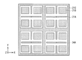
- FIG. 2 is a schematic plan view illustrating an example of a layout of a lower electrode included in the organic photoelectric conversion unit illustrated in FIG. 1.
- FIG. 5B is a perspective view showing the layout of the lower electrode shown in FIG. 5A.
- FIG. 5A is a perspective view showing the layout of the lower electrode shown in FIG. 5A.
- FIG. 2 is a schematic plan view illustrating another example of a layout of a lower electrode included in the organic photoelectric conversion unit illustrated in FIG. 1.
- FIG. 5B is a perspective view showing the layout of the lower electrode shown in FIG. 5A.
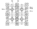
- FIG. 2 is a schematic plan view illustrating an example of a layout of one inorganic photoelectric conversion unit illustrated in FIG. 1 and various transistors related thereto.
- FIG. 2 is a schematic plan view illustrating an example of a layout of another inorganic photoelectric conversion unit illustrated in FIG. 1 and various transistors related thereto.
- FIG. 2 is a signal line layout diagram for driving a storage electrode shown in FIG. 1. It is a figure showing a part of wiring connected to an adjacent photoelectric conversion part and various transistors related to this.
- FIG. 2 is a cross-sectional view for describing a method for manufacturing the imaging device illustrated in FIG. 1.
- FIG. 14 is a schematic sectional view illustrating a step following FIG. 13.
- FIG. 15 is a schematic sectional view illustrating a step following FIG. 14.
- FIG. 16 is a schematic sectional view illustrating a step following FIG. 15.
- FIG. 2 is a timing chart illustrating an operation example of the imaging device illustrated in FIG. 1.
- FIG. 9 is a schematic cross-sectional view illustrating a configuration of a main part of an imaging element according to a second embodiment of the present disclosure.
- FIG. 14 is a schematic cross-sectional view illustrating a configuration of a main part of an imaging element according to a third embodiment of the present disclosure.
- FIG. 14 is a schematic cross-sectional view illustrating a configuration of a main part of an image sensor according to a fourth embodiment of the present disclosure.
- FIG. 11 is a schematic plan view illustrating another example of a layout of a lower electrode included in an organic photoelectric conversion unit according to a modified example of the present disclosure.
- FIG. 11 is a schematic plan view illustrating another example of a layout of one inorganic photoelectric conversion unit and various transistors related thereto according to a modified example of the present disclosure.
- FIG. 11 is a schematic plan view illustrating another example of a layout of another inorganic photoelectric conversion unit according to a modified example of the present disclosure and various transistors related thereto.
- FIG. 11 is a diagram illustrating another example of a wiring connected to a photoelectric conversion unit and various transistors related thereto according to a modification example of the present disclosure.
- FIG. 11 is a diagram illustrating another example of a wiring connected to a photoelectric conversion unit and various transistors related thereto according to a modification example of the present disclosure.
- FIG. 11 is a schematic plan view illustrating another example of a layout of one inorganic photoelectric conversion unit and various transistors related thereto according to a modified example of the present disclosure.
- FIG. 11 is a schematic plan view illustrating another example of a layout of another inorganic photoelectric conversion unit according to a
- FIG. 11 is a diagram illustrating another example of a wiring connected to a photoelectric conversion unit and various transistors related thereto according to a modification example of the present disclosure.
- FIG. 11 is a diagram illustrating another example of a wiring connected to a photoelectric conversion unit and various transistors related thereto according to a modification example of the present disclosure.
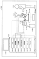
- FIG. 2 is a block diagram illustrating a configuration of an imaging device using the imaging device illustrated in FIG. 1 and the like as pixels.
- FIG. 29 is a functional block diagram illustrating an example of an electronic apparatus (camera) using the imaging device illustrated in FIG. 28. It is a block diagram which shows an example of a schematic structure of an in-vivo information acquisition system. It is a figure showing an example of the schematic structure of an endoscope operation system.
- FIG. 1 is a block diagram illustrating another example of a wiring connected to a photoelectric conversion unit and various transistors related thereto according to a modification example of the present disclosure.
- FIG. 2 is a block diagram illustrating a
- FIG. 3 is a block diagram illustrating an example of a functional configuration of a camera head and a CCU. It is a block diagram showing an example of a schematic structure of a vehicle control system. It is explanatory drawing which shows an example of the installation position of a vehicle exterior information detection part and an imaging part.
- Third embodiment an example in which a first hydrogen block layer and a second hydrogen block layer are directly stacked in a peripheral region
- Fourth embodiment an example in which an insulating layer on a lower electrode is formed as a second hydrogen block layer
- Modified example other example of pixel layout
- Application example 7 Application examples
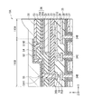
- FIG. 1 illustrates a cross-sectional configuration of an imaging device (imaging device 10A) according to the first embodiment of the present disclosure.
- FIG. 2 illustrates a cross-sectional configuration of a main part of the image sensor 10A illustrated in FIG.
- FIG. 3 is an equivalent circuit diagram of the image sensor 10A shown in FIG.
- FIG. 4 schematically shows the arrangement of the lower electrode 21 of the image sensor 10 and the transistors constituting the control unit shown in FIG.
- the image pickup device 10A is, for example, a single pixel (unit pixel P) in an image pickup device (image pickup device 1; see FIG. 28) such as a CMOS (Complementary Metal Oxide Semiconductor) image sensor used for electronic devices such as digital still cameras and video cameras.
- CMOS Complementary Metal Oxide Semiconductor
- the imaging device 1 has an effective pixel area 110A in which a plurality of pixels are arranged, and a peripheral area 110B provided around the effective pixel area 110A and in which peripheral circuits such as the row scanning unit 131 are formed.
- An image sensor 10A is formed in each of the plurality of pixels.
- the image pickup device 10A of the present embodiment is one in which the organic photoelectric conversion unit 20 is provided on the light receiving surface (first surface; surface 30S1) of the semiconductor substrate 30, and the organic photoelectric conversion unit 20 is arranged from the semiconductor substrate 30 side.
- a lower electrode 21 (first electrode) composed of a plurality of electrodes, an insulating layer 22, a charge storage layer 23, a photoelectric conversion layer 24 (organic photoelectric conversion layer), and an upper electrode 25 (second electrode) laminated in this order.
- the stacked charge accumulation layer 23 and photoelectric conversion layer 24 are formed to extend in the effective pixel region 110A as a common layer for a plurality of pixels provided in the effective pixel region 110A.
- the image sensor 10A has a pixel sharing structure in which four adjacent pixels share one corresponding floating diffusion FD1, FD2, or FD3.
- the imaging device 10A is, for example, a so-called vertical spectral imaging device in which one organic photoelectric conversion unit 20 and two inorganic photoelectric conversion units 32B and 32R are vertically stacked.
- the organic photoelectric conversion unit 20 is provided on the first surface (back surface; surface 30S1) side of the semiconductor substrate 30 as described above.
- the inorganic photoelectric conversion units 32B and 32R are embedded in the semiconductor substrate 30 and stacked in the thickness direction of the semiconductor substrate 30.
- the organic photoelectric conversion unit 20 has a charge storage layer 23 and a photoelectric conversion layer 24 between a lower electrode 21 and an upper electrode 25 which are arranged opposite to each other, as will be described in detail later.
- the insulating layer 22 is provided between the two.
- the lower electrode 21 is composed of a plurality of electrodes (readout electrode 21A, storage electrode 21B, and shield electrode 21C).
- the read electrode 21A is electrically connected to the charge storage layer 23 through an opening 22H formed in the insulating layer 22.
- the photoelectric conversion layer 24 includes a p-type semiconductor and an n-type semiconductor, and has a bulk heterojunction structure in the layer.
- the bulk heterojunction structure is a p / n junction surface formed by mixing a p-type semiconductor and an n-type semiconductor.
- the organic photoelectric conversion unit 20 and the inorganic photoelectric conversion units 32B and 32R perform photoelectric conversion by selectively detecting light in different wavelength ranges. Specifically, for example, the organic photoelectric conversion unit 20 acquires a green (G) color signal.
- the inorganic photoelectric conversion units 32B and 32R acquire blue (B) and red (R) color signals, respectively, depending on the difference in the absorption coefficient. Thereby, in the image sensor 10A, a plurality of types of color signals can be obtained in one pixel without using a color filter.
- this embodiment mode describes a case where electrons are read out as signal charges from an electron-hole pair (electron-hole pair) generated by photoelectric conversion (a case where an n-type semiconductor region is used as a photoelectric conversion layer). I do.
- “+ (plus)” added to “p” and “n” indicates that the p-type or n-type impurity concentration is high.
- the semiconductor substrate 30 On the second surface (front surface; 30S2) of the semiconductor substrate 30, for example, a floating diffusion (floating diffusion layer) FD1 (region 35 in the semiconductor substrate 30), FD2, FD3, transfer transistors TR2trs, TR3trs, and an amplifier transistor ( (Modulation elements) TR1amp and TR2amp, reset transistors TR1rst and TR2rst, select transistors TR1sel and TR2sel, and a multilayer wiring 40.
- the multilayer wiring 40 has, for example, a configuration in which wiring layers 41, 42, and 43 are stacked in an insulating layer 44.
- the first surface (surface 30S1) side of the semiconductor substrate 30 is referred to as a light incident side S1
- the second surface (surface 30S2) side is referred to as a wiring layer side S2.
- the organic photoelectric conversion unit 20 is configured such that the lower electrode 21, the insulating layer 22, the charge storage layer 23, the photoelectric conversion layer 24, and the upper electrode 25 are formed from the first surface (the surface 30S1) of the semiconductor substrate 30. It has a configuration stacked in this order.
- the lower electrode 21 is formed, for example, separately from the readout electrode 21A and the storage electrode 21B separated from each other with the insulating layer 22 interposed therebetween and the shield electrode 21C surrounding four pixels adjacent to each other, while being formed separately for each imaging element 10A. It is configured.
- the readout electrode 21A is shared by two or four pixels adjacent to each other and has an opening 22H provided in the insulating layer 22, as shown in FIGS. 5A and 6A, for example.
- the charge storage layer 23, the photoelectric conversion layer 24, and the upper electrode 25 are provided as a continuous layer common to the plurality of imaging elements 10A, and extend to the effective pixel region 110A.
- a hydrogen block layer 26 is further provided on the upper electrode 25. The hydrogen block layer 26 is stacked on the insulating layer 22 from above the upper electrode 25 via the side surfaces of the upper electrode 25, the photoelectric conversion layer 24, and the charge storage layer 23, for example, in the peripheral region 110B.
- a fixed charge layer 27 Between the first surface (surface 30S1) of the semiconductor substrate 30 and the lower electrode 21, for example, a fixed charge layer 27, an insulating layer 28, and an interlayer insulating layer 29 are provided in this order.
- a first protective layer 51, a second protective layer 53, and an on-chip lens layer 56 are provided in this order.
- the wiring 52 is provided between the first protective layer 51 and the second protective layer 53, and the light shielding film 54 is provided between the second protective layer 53 and the on-chip lens layer 56.
- Through electrodes 34A, 34B, 34C, 34D are provided between the first surface (surface 30S1) and the second surface (surface 30S2) of the semiconductor substrate 30.
- the through electrode 34A is electrically connected to the readout electrode 21A of the organic photoelectric conversion unit 20, and the organic photoelectric conversion unit 20 is connected via the through electrode 34 to, for example, the gate Gamp of the amplifier transistor TR1amp and the floating diffusion FD1.
- the penetrating electrode 34B is electrically connected to the storage electrode 21B of the organic photoelectric conversion unit 20, so that a voltage can be applied to the storage electrode 21B independently of the readout electrode 21A.
- the through-electrode 34C is electrically connected to the shield electrode 21C, thereby suppressing charge leakage to an adjacent pixel.
- the through electrode 34D is electrically connected to the pad 36D provided in the peripheral region 110B.
- the wiring 52 is electrically connected to the pad portion 36D via the opening 51H1, and forms a guard ring 55.
- a voltage can be applied to the upper electrode 25.
- the guard ring 55 can prevent water from entering from the outer periphery.
- the wiring 52 forming the guard ring 55 does not necessarily need to be electrically connected to the upper electrode 25.
- FIG. 2 shows an example in which the second protective layer 53 is embedded in the opening 51H1 forming the guard ring 55.
- the present invention is not limited to this.
- the hydrogen blocking layer 26 and the first protective layer 51 are embedded. May be.
- the lower ends of the through electrodes 34A, 34B, 34C, 34D are connected to the wiring layer 41, respectively.
- the through electrode 34A is connected to the connection portion 41A in the wiring layer 41, and the connection portion 41A and the floating diffusion FD1 (region 35) are connected, for example, via the lower first contact 45.
- the upper end of the through electrode 34A is connected to the readout electrode 21A via, for example, a pad 35A, a via V2, a pad 36A, and a via V1.
- the through-electrode 34A is provided, for example, one for each of four pixels adjacent to each other.
- the through electrode 34A has a function as a connector between the organic photoelectric conversion unit 20 of each pixel and the gate Gamp of the amplifier transistor TR1amp and the floating diffusion FD1, and at the same time, a charge (here, electrons) generated in the organic photoelectric conversion unit 20. It is a transmission path.
- the reset gate Grst of the reset transistor TR1rst is arranged next to the floating diffusion FD1 (one source / drain region of the reset transistor TR1rst). This makes it possible to reset the charge accumulated in the floating diffusion FD1 by the reset transistor TR1rst.
- the imaging device 10A of the present embodiment light incident on the organic photoelectric conversion section 20 from the upper electrode 25 side is absorbed by the photoelectric conversion layer 24.
- the excitons thus generated move to the interface between the electron donor and the electron acceptor constituting the photoelectric conversion layer 24, and exciton separation, that is, dissociation into electrons and holes.
- the charges (electrons and holes) generated here are diffused due to a difference in carrier concentration or due to an internal electric field due to a difference in work function between an anode (here, the upper electrode 25) and a cathode (here, the lower electrode 21). Each is carried to a different electrode and detected as a photocurrent. Further, by applying a potential between the lower electrode 21 and the upper electrode 25, the transport direction of electrons and holes can be controlled.
- the organic photoelectric conversion unit 20 absorbs green light corresponding to part or all of a selective wavelength range (for example, 450 nm or more and 650 nm or less) to generate an electron-hole pair. It is.
- a selective wavelength range for example, 450 nm or more and 650 nm or less
- the lower electrode 21 is composed of the readout electrode 21A, the storage electrode 21B, and the shield electrode 21C which are formed separately as described above.
- the readout electrode 21A is for transferring electric charges (here, electrons) generated in the photoelectric conversion layer 24 to the floating diffusion FD1, and includes, for example, a via V1, a pad portion 36A, a via V2, a pad portion 35A, a penetrating portion. It is connected to the floating diffusion FD1 via the electrode 34, the connecting portion 41A and the lower first contact 45.
- the storage electrode 21 ⁇ / b> B is for storing electrons in the charge storage layer 23 as signal charges among charges generated in the photoelectric conversion layer 24.
- the storage electrode 21B is provided in a region that covers the light receiving surfaces of the inorganic photoelectric conversion units 32B and 32R formed in the semiconductor substrate 30 and faces these light receiving surfaces.
- the storage electrode 21B is preferably larger than the readout electrode 21A, so that a large amount of charges can be stored.
- the shield electrode 21C is for suppressing charge leakage to the adjacent pixel.
- the lower electrode 21 is made of a light-transmitting conductive film, and is made of, for example, ITO (indium tin oxide).
- ITO indium tin oxide
- a tin oxide (SnO 2 ) -based material to which a dopant is added or a zinc oxide-based material obtained by adding a dopant to zinc oxide (ZnO) is used. May be used.
- the zinc oxide-based material include aluminum zinc oxide (AZO) to which aluminum (Al) is added as a dopant, gallium zinc oxide (GZO) to which gallium (Ga) is added, and indium zinc oxide to which indium (In) is added. (IZO).
- the thickness of the lower electrode 21 is preferably, for example, 20 nm to 200 nm, and more preferably 30 nm or more and 100 nm or less.
- the insulating layer 22 is for electrically insulating the storage electrode 21B from the charge storage layer 23.
- the insulating layer 22 is provided, for example, on the interlayer insulating layer 29 and the lower electrode 21 so as to cover the lower electrode 21.
- an opening 22H is provided on the reading electrode 21A among the lower electrodes 21, and the reading electrode 21A and the charge storage layer 23 are electrically connected through the opening 22H.
- the insulating layer 22 is, for example, a single-layer film made of one of silicon oxide (SiO x ), silicon nitride (SiN x ), silicon oxynitride (SiO x N y ), and the like, or a single layer film thereof. It is composed of two or more kinds of laminated films.
- the thickness of the insulating layer 22 is, for example, 20 nm to 500 nm.
- the charge storage layer 23 is provided below the photoelectric conversion layer 24, specifically, between the insulating layer 22 and the photoelectric conversion layer 24, and stores signal charges (here, electrons) generated in the photoelectric conversion layer 24. It is for doing.
- the charge storage layer 23 is preferably formed using a material having a higher charge mobility and a larger band gap than the photoelectric conversion layer 24.
- the band gap of the constituent material of the charge storage layer 23 is preferably 3.0 eV or more.
- examples of such a material include an oxide semiconductor material such as IGZO and an organic semiconductor material.
- the organic semiconductor material include transition metal dichalcogenide, silicon carbide, diamond, graphene, carbon nanotube, condensed polycyclic hydrocarbon compound, condensed heterocyclic compound, and the like.
- the thickness of the charge storage layer 23 is, for example, not less than 10 nm and not more than 300 nm.
- the photoelectric conversion layer 24 converts light energy into electric energy.
- the photoelectric conversion layer 24 includes, for example, two or more types of organic materials (p-type semiconductor materials or n-type semiconductor materials) each functioning as a p-type semiconductor or an n-type semiconductor.
- the photoelectric conversion layer 24 has a bonding surface (p / n bonding surface) between the p-type semiconductor material and the n-type semiconductor material in the layer.
- the p-type semiconductor relatively functions as an electron donor (donor), and the n-type semiconductor relatively functions as an electron acceptor (acceptor).
- the photoelectric conversion layer 24 provides a field where excitons generated when light is absorbed are separated into electrons and holes, and specifically, an interface (p / p) between an electron donor and an electron acceptor. At the (n-junction surface), the exciton separates into electrons and holes.
- the photoelectric conversion layer 24 includes, in addition to the p-type semiconductor material and the n-type semiconductor material, an organic material that photoelectrically converts light in a predetermined wavelength band and transmits light in another wavelength band, a so-called dye material. It may be. In the case where the photoelectric conversion layer 24 is formed using three types of organic materials, a p-type semiconductor material, an n-type semiconductor material, and a dye material, the p-type semiconductor material and the n-type semiconductor material are in a visible region (for example, 450 nm to (800 nm). The thickness of the photoelectric conversion layer 24 is, for example, 50 nm to 500 nm.
- Examples of the organic material constituting the photoelectric conversion layer 24 include quinacridone, chlorinated boron subphthalocyanine, pentacene, benzothienobenzothiophene, fullerene, and derivatives thereof.
- the photoelectric conversion layer 24 is configured by combining two or more of the above organic materials.
- the organic material functions as a p-type semiconductor or an n-type semiconductor depending on the combination.
- the organic material forming the photoelectric conversion layer 24 is not particularly limited. In addition to the organic materials described above, for example, any one of naphthalene, anthracene, phenanthrene, tetracene, pyrene, perylene, and fluoranthene or a derivative thereof is preferably used. Alternatively, polymers such as phenylenevinylene, fluorene, carbazole, indole, pyrene, pyrrole, picoline, thiophene, acetylene, and diacetylene, and derivatives thereof may be used.
- metal complex dyes cyanine dyes, merocyanine dyes, phenylxanthene dyes, triphenylmethane dyes, rhodacyanine dyes, xanthene dyes, macrocyclic azaannulene dyes, azulene dyes, naphthoquinones, anthraquinone dyes, Condensed polycyclic aromatic and aromatic or heterocyclic compounds such as anthracene and pyrene, or a chain compound condensed with two or more quinoline, benzothiazole, benzoxazole, etc.
- a nitrogen heterocycle, or a cyanine-like dye linked by a squarylium group and a croconite methine group can be preferably used.
- the metal complex dye is preferably a dithiol metal complex dye, a metal phthalocyanine dye, a metal porphyrin dye, or a ruthenium complex dye, but is not limited thereto.
- a charge storage layer 23 an electron blocking film, a photoelectric conversion layer 24, a hole blocking film, a work function adjusting layer, and the like may be stacked in this order from the lower electrode 21 side.
- an undercoat layer and a hole transport layer may be provided between the lower electrode 21 and the photoelectric conversion layer 24, and a buffer layer and an electron transport layer may be provided between the photoelectric conversion layer 24 and the upper electrode 25.
- the upper electrode 25 is made of a conductive film having optical transparency, like the lower electrode 21. In the imaging device 1 using the imaging element 10A as one pixel, the upper electrode 25 may be separated for each pixel, or may be formed as a common electrode for each pixel. The thickness of the upper electrode 25 is, for example, 10 nm to 200 nm. As shown in FIG. 2, a wiring 52 is electrically connected to the upper electrode 25 via, for example, an opening 51H2. The wiring 52 is also electrically connected to the pad portion 36D through the opening 51H1, as shown in FIG. That is, the upper electrode 25 is electrically connected to the pad portion 36D via the wiring 52, for example.
- the hydrogen blocking layer 26 is for suppressing the intrusion of hydrogen (H 2 ) into the charge storage layer 23.
- the hydrogen blocking layer 26 is provided on the upper electrode 25 in the effective pixel region 110A, and is provided on the peripheral region 110B.
- the insulating layer 22 is stacked on the insulating layer 22 from the upper surface of the upper electrode 25 via the side surfaces of the upper electrode 25, the photoelectric conversion layer 24, and the charge storage layer 23, and is formed to extend, for example, to the end of the peripheral region 110B.
- Examples of the material forming the hydrogen blocking layer 26 include an insulating material. Specifically, it is preferable to use a material having a light-transmitting property and a high sealing property.
- Examples of such a material include a metal oxide such as aluminum oxide (AlO x ) and silicon nitride (SiN x). ), Carbon-containing silicon oxide (SiOC), and the like.
- a metal oxide such as aluminum oxide (AlO x ) and silicon nitride (SiN x).
- SiOC Carbon-containing silicon oxide
- an oxide semiconductor such as ITO (indium tin oxide) may be used.
- the hydrogen blocking layer 26 has, for example, a lower hydrogen content than the insulating layer 22 or the film itself does not contain hydrogen. Further, it is preferable that the hydrogen blocking layer 26 has a small stress and further has an ultraviolet absorbing ability. Furthermore, it is preferable to form a film containing a small amount of water and to suppress the intrusion of water (H 2 O).
- the hydrogen blocking layer 26 is formed of a single-layer film formed using the above-described material or a laminated film including two or more of the above-described materials.
- the thickness of the hydrogen blocking layer 26 is, for example, not less than 10 nm and not more than 1000 nm.
- the fixed charge layer 27 may be a film having a positive fixed charge or a film having a negative fixed charge.
- Materials for the film having a negative fixed charge include hafnium oxide (HfO x ), aluminum oxide (AlO x ), zirconium oxide (ZrO x ), tantalum oxide (TaO x ), titanium oxide (TiO x ), and lanthanum oxide ( LaO x ), praseodymium oxide (PrO x ), cerium oxide (CeO x ), neodymium oxide (NdO x ), promethium oxide (PmO x ), samarium oxide (SmO x ), europium oxide (EuO x ), gadolinium oxide (GdO) x), terbium oxide (TBO x), dysprosium oxide (DyO x), holmium oxide (HoO x), thulium oxide (TMO x), ytterb
- the fixed charge layer 27 may have a configuration in which two or more types of films are stacked. Thereby, for example, in the case of a film having a negative fixed charge, the function as a hole accumulation layer can be further enhanced.
- the insulating layer 28 is formed on the fixed charge layer 27 formed on the first surface (the surface 30S1) of the semiconductor substrate 30 and in the through holes 30H1, 30H2, 30H3, and 30H4 in which the through electrodes 34A, 34B, 34C, and 34D are formed. It is provided between the fixed charge layer 27 and the through electrodes 34A, 34B, 34C, 34D, and is for electrically insulating the through electrode 34 and the semiconductor substrate 30 from each other.
- the material of the insulating layer 28 is not particularly limited.
- the insulating layer 28 is formed of silicon oxide (SiO x ), TEOS, silicon nitride (SiN x ), silicon oxynitride (SiO x N y ), or the like.
- the interlayer insulating layer 29 is a single layer made of, for example, one of silicon oxide (SiO x ), TEOS, silicon nitride (SiN x ), silicon oxynitride (SiO x N y ), and the like. It is composed of a film or a laminated film composed of two or more of these.
- pad portions 35C and 36C for electrically connecting the shield electrode 21C and the through electrode 34C, pad portions 35D and 36D for electrically connecting the wiring 52 and the through electrode 34D, and electrically connecting each electrode and the pad portion.
- the first protection layer 51 and the second protection layer 53 are provided on the entire surface of the semiconductor substrate 30 including the effective pixel region 110A and the peripheral region 110B, for example. It is preferable that the first protective layer 51 and the second protective layer 53 are formed using, for example, a material having a light-transmitting property and a high sealing property. Examples of such a material include insulating materials such as aluminum oxide (AlO x ), silicon nitride (SiN x ), and carbon-containing silicon oxide (SiOC).
- the first protective layer 51 and the second protective layer 53 preferably have a lower hydrogen content than the insulating layer 22, for example, as in the case of the hydrogen blocking layer 26, or the films themselves do not contain hydrogen.
- first protective layer 51 and the second protective layer 53 have a small stress and further have an ultraviolet absorbing ability. Furthermore, it is preferable that the first protective layer 51 and the second protective layer 53 contain a small amount of water, and it is preferable to suppress intrusion of water (H 2 O). From the above, it is preferable to use aluminum oxide (AlO x ) among the above materials as the material of the first protective layer 51 and the second protective layer 53.
- AlO x aluminum oxide
- the first protective layer 51 and the second protective layer 53 may be formed using the same material as that of the insulating layer 28 and the interlayer insulating layer 29.
- the first protective layer 51 and the second protective layer 53 are single-layer films made of one of silicon oxide (SiO x ), silicon nitride (SiN x ), silicon oxynitride (SiO x N y ), and the like. Or two or more of aluminum oxide (AlO x ), silicon nitride (SiN x ), carbon-containing silicon oxide film (SiOC), silicon oxide (SiO x ), and silicon oxynitride (SiO x N y ) It may be a laminated film.
- the thickness of the first protective layer 51 is, for example, 100 nm to 1000 nm.
- the thickness of the second protective layer 53 is, for example, 10 nm to 1000 nm.
- the wiring 52 is provided on the second protective layer 53 in the peripheral region 110B. As described above, the wiring 52 is electrically connected to the upper electrode 25 via the opening 51H2 penetrating the first protective layer 51 and the hydrogen block layer 26, for example.
- the wiring 52 is electrically connected to the pad portion 36D provided in the interlayer insulating layer 29 through the opening 51H1 penetrating through the first protective layer 51, the hydrogen blocking layer 26, and the insulating layer 22 in the peripheral region 110B.
- a guard ring 55 is formed.
- the pad portion 36D is connected to a through electrode 34D that penetrates the via V2, the pad portion 35D, and the semiconductor substrate 30 and is connected to the wiring layer 41 provided on the second surface (surface 30S2) side of the semiconductor substrate 30. Thereby, it functions as a transmission path for charges (here, holes) generated in the organic photoelectric conversion unit 20.
- the light-shielding film 54 is provided on the second protective layer 53 in the peripheral region 110B.
- Examples of the material of the light-shielding film 54 include tungsten (W), titanium (Ti), titanium nitride (TiN), and aluminum (Al).
- the light-shielding film 54 is, for example, a laminated film of W / TiN / Ti or W As a single-layer film.
- the thickness of the light shielding film 54 is, for example, not less than 50 nm and not more than 400 nm.
- an on-chip lens layer 56 in which the on-chip lens 56L (microlens) is formed for each unit pixel P in the effective pixel region 110A is provided.
- the on-chip lens 56L collects light incident from above onto the respective light receiving surfaces of the organic photoelectric conversion unit 20, the inorganic photoelectric conversion unit 32B, and the inorganic photoelectric conversion unit 32R.
- an optical member such as a color filter for controlling the spectral distribution may be provided below the on-chip lens 56L.
- the semiconductor substrate 30 is formed of, for example, an n-type silicon (Si) substrate, and has a p-well 31 in a predetermined region (for example, the pixel unit 1a).
- the transfer transistor TR1trs, TR2trs, TR3trs, the amplifier transistors TR1amp, TR2amp, the reset transistors TR1rst, TR2rst, the selection transistors TR1sel, TR2sel, and the like are provided on the second surface (the surface 30S2) of the p-well 31.
- a pixel readout circuit, a pixel drive circuit, and the like, which are formed by a logic circuit, are provided in the peripheral region 110B of the semiconductor substrate 30, for example.
- FIG. 5A illustrates an example of a layout of the lower electrode 21 included in the organic photoelectric conversion unit 20, and FIG. 5B illustrates a layout of the lower electrode 21 illustrated in FIG. 5A as a transparent perspective view.
- 6A illustrates an example of a layout of the lower electrode 21 included in the organic photoelectric conversion unit 20, and FIG. 6B illustrates a layout of the lower electrode 21 illustrated in FIG. 6A as a transparent perspective view.
- FIG. 7 illustrates an example of a layout of the inorganic photoelectric conversion unit 32B and various transistors related thereto.
- FIG. 8 illustrates an example of a layout of the inorganic photoelectric conversion unit R and various transistors related thereto.
- FIG. 9 illustrates an example of signal wiring for driving the storage electrode 21 ⁇ / b> B in the organic photoelectric conversion unit 20.
- FIGS. 10 to 12 show an example of wiring connected to each of the photoelectric conversion units 20, 32B, 32R and various transistors related thereto.
- the organic photoelectric conversion unit 20 of the present embodiment four adjacent organic photoelectric conversion units 20 are connected to one floating diffusion FD1.
- One reset transistor TR1rst and a power supply line Vdd are connected in series to the floating diffusion FD1.
- one of the amplifier transistor TR1amp and one of the selection transistor TR1sel and a signal line (data output line) VSL1 are connected in series to the floating diffusion FD1.
- four storage electrodes 21B adjacent to each other and a reset transistor TR1rst, an amplifier transistor TR1amp, and a selection transistor TR1sel provided one for each pixel are adjacent to each other.
- a set of control units (first control units) responsible for the read operation and the reset operation of the four organic photoelectric conversion units 20 is configured.
- the first control unit is used, for example, to perform the reading process sequentially in a time-division manner.
- inorganic photoelectric conversion unit 32B of the present embodiment four photodiodes PD2 adjacent to each other are connected to one floating diffusion FD2 via four transfer transistors TR2trs provided one for each pixel. I have.
- inorganic photoelectric conversion unit 32R of the present embodiment similarly to the inorganic photoelectric conversion unit 32B, four photodiodes PD3 adjacent to each other are connected via four transfer transistors TR3trs provided one for each pixel. It is connected to one floating diffusion FD3.
- One reset transistor TR2rst and one power supply line Vdd are connected in series to one floating diffusion FD2. Apart from this, one of the amplifier transistor TR2amp and one of the selection transistor TR2sel and a signal line (data output line) VSL2 are connected in series to the floating diffusion FD2.
- the inorganic photoelectric conversion unit 32B and the inorganic photoelectric conversion unit 32R are provided with the transfer transistor TR2trs and the transfer transistor TR3trs provided for each pixel, and for each pixel.
- the reset transistor TR2rst, the amplifier transistor TR2amp, and the selection transistor TR2sel each of which is provided one by one, provide a set of control units (for a read operation and a reset operation of the four inorganic photoelectric conversion units 32B and 32R adjacent to each other).
- a second control unit That is, in the four inorganic photoelectric conversion units 32B and the four inorganic photoelectric conversion units 32R provided in the stacked imaging device 10A for four pixels, one set of the control unit (the second control unit) except the transfer transistors TR2trs and TR3trs. Part) is shared.
- the second control unit When reading out the signal charges from the floating diffusion FD2 corresponding to the four inorganic photoelectric conversion units 32B adjacent to each other and the floating diffusion FD3 corresponding to the four inorganic photoelectric conversion units 32R, the second control unit is used, for example. The reading process is performed sequentially in time division.
- the floating diffusions FD2 and FD3 which are shared by the four inorganic photoelectric conversion units 32B and 32R adjacent to each other, are arranged at locations separated by one pixel each. This makes it possible to achieve high integration of the imaging element 10A.
- the image sensor 10A of the present embodiment can be manufactured, for example, as follows.
- a p-well 31 is formed as a well of a first conductivity type in a semiconductor substrate 30, and inorganic photoelectric conversion units 32 B and 32 R of a second conductivity type (for example, n-type) are formed in the p-well 31. I do.
- a p + region is formed near the first surface (surface 30S1) of the semiconductor substrate 30.
- a gate insulating layer 33 On the second surface (surface 30S2) of the semiconductor substrate 30, for example, after forming n + regions serving as floating diffusions FD1 to FD3, a gate insulating layer 33, various transfer transistors TR1trs, TR2trs, TR3trs, select transistors TR1sel, TR2sel, A gate wiring layer 47 including the gates of the amplifier transistors TR1amp and TR2amp and the reset transistors TR1rst and TR2rst is formed. Thus, various transfer transistors TR1trs, TR2trs, TR3trs, select transistors TR1sel, TR2sel, amplifier transistors TR1amp, TR2amp, and reset transistors TR1rst, TR2rst are formed. Further, on the second surface (surface 30S2) of the semiconductor substrate 30, the multilayer wiring 40 including the wiring layers 41 to 43 including the lower first contact 45 and the connection portion 41A and the insulating layer 44 is formed.
- an SOI (Silicon On Insulator) substrate in which the semiconductor substrate 30, a buried oxide film (not shown), and a holding substrate (not shown) are laminated is used as the base of the semiconductor substrate 30.
- the buried oxide film and the holding substrate are joined to the first surface (surface 30S1) of the semiconductor substrate 30. After the ion implantation, an annealing process is performed.
- a support substrate (not shown) or another semiconductor substrate is bonded to the second surface (surface 30S2) side (multilayer wiring 40 side) of the semiconductor substrate 30, and the semiconductor substrate 30 is turned upside down.
- the semiconductor substrate 30 is separated from the buried oxide film of the SOI substrate and the holding substrate, and the first surface (the surface 30S1) of the semiconductor substrate 30 is exposed.
- the above steps can be performed by a technique used in a normal CMOS process such as ion implantation and CVD (Chemical Vapor Deposition).
- the semiconductor substrate 30 is processed from the first surface (surface 30S1) side by, for example, dry etching to form, for example, annular through holes 30H1, 30H2, 30H3, and 30H4.
- the depth of the through holes 30H1 to 30H4 penetrates from the first surface (the surface 30S1) to the second surface (the surface 30S2) of the semiconductor substrate 30.
- the fixed charge layer 27 is formed on the first surface (the surface 30S1) and the side surface of the through hole 30H of the semiconductor substrate 30 by using, for example, an atomic layer deposition (ALD) method.
- ALD atomic layer deposition
- the fixed charge layer 27 that is continuous with the first surface (the surface 30S1) of the semiconductor substrate 30 and the side surfaces and the bottom surfaces of the through holes 30H1, 30H2, 30H3, and 30H4 is formed.
- the insulating layer 28 is formed on the first surface (the surface 30S1) of the semiconductor substrate 30 of the fixed charge layer 27 and in the through holes 30H1, 30H2, 30H3, and 30H4, an interlayer is further formed on the insulating layer 28.
- An insulating film for forming the insulating layer 29 is formed.
- the insulating film constituting the interlayer insulating layer 29, the insulating layer 28, the fixed charge layer 27, and the insulating layer 44 are formed.
- a through hole that penetrates and reaches the connection portion 41A is formed.
- the insulating film constituting the interlayer insulating layer 29 on the first surface (the surface 30S1) is also reduced in thickness.
- a photoresist PR is formed at a predetermined position on the conductive film.
- electrodes 34A, 34B, 34C, 34D having pad portions 35A, 35B, 35C, 35D are formed on the first surface (surface 30S1) of the semiconductor substrate 30. You.
- a via V2, pad portions 36, 36B, 36C, 36D, and a via V1 are formed on the insulating film and the through electrodes 34A, 34B, 34C, 34D forming the interlayer insulating layer 29, respectively, and then the CMP (Chemical @ Mechanical). Polishing), the surface of the interlayer insulating layer 29 is flattened. Subsequently, after a conductive film is formed on the interlayer insulating layer 29, a photoresist PR is formed at a predetermined position of the conductive film. Thereafter, the readout electrode 21A, the storage electrode 21B, and the shield electrode 21C are formed by etching and removing the photoresist PR.
- an opening 22H is provided on the readout electrode 21A.
- the charge storage layer 23, the photoelectric conversion layer 24, and the upper electrode 25 are formed on the insulating layer 22.
- the charge storage layer 23 and other organic layers are formed using an organic material, it is desirable that the charge storage layer 23 and other organic layers be formed continuously in a vacuum process (in a consistent vacuum process).
- the method for forming the photoelectric conversion layer 24 is not necessarily limited to the method using the vacuum evaporation method, but may be another method, for example, a spin coating technique or a printing technique.
- an aluminum oxide (AlO x ) film 26B is formed as a hard mask on the effective pixel region 110A on the upper electrode 25 by, for example, a physical vapor deposition (PVD) method. It is formed with a thickness of, for example, 10 nm to 50 nm. Note that the film formation method is not limited to this, and for example, a CVD method or an ALD method may be used.
- Examples of the film forming method of the PVD method include EB (electron beam) evaporation method, various sputtering methods (magnetron sputtering method, RF-DC combined bias sputtering method, ECR sputtering method, facing target sputtering method, high frequency sputtering method) and the like. Is mentioned.
- EB electron beam
- various sputtering methods magnetotron sputtering method, RF-DC combined bias sputtering method, ECR sputtering method, facing target sputtering method, high frequency sputtering method
- the PVD / ALD method has excellent coverage.
- the deposition rate of the CVD / ALD method is significantly lower than that of the PVD method. Therefore, if the upper electrode 25 can be sufficiently covered by the PVD method, it is preferable to use the PVD method.
- the AlO x film 26B is patterned using, for example, a lithography method to form a hard mask.
- FIG. 14 described later shows an example in which the photoresist PR is removed, the following process may be performed with the resist remaining after patterning the AlO x film 26B.
- the charge storage layer 23, the photoelectric conversion layer 24, and the upper electrode 25 formed in the peripheral region 110B are etched.
- an AlO x film 26A is formed to a thickness of, for example, 50 nm to 1000 nm by using, for example, the PVD method.
- a hydrogen block layer 26 composed of the AlO x films 26A and 26B is formed.
- the AlO x film 26A may be formed by a CVD method or an ALD method similarly to the AlO x film 26B. For example, when the step of the charge storage layer 23, the photoelectric conversion layer 24, and the upper electrode 25 is large.
- the hydrogen blocking layer 26 composed of a laminated film may be formed by combining the PVD method and the CVD / ALD method.
- a photoresist PR is patterned on the first protective layer 51, and is electrically connected to the through electrode 34D in the peripheral region 110B.
- An opening 51H1 penetrating to the pad portion 36D is formed.
- an opening 51H2 penetrating to the upper electrode 25 is formed. Note that the order of forming the openings 51H1 and 51H2 is not limited to this, and for example, the openings 51H1 and 51H2 may be formed simultaneously.
- the imaging device 10A when light enters the organic photoelectric conversion unit 20 via the on-chip lens 56L, the light passes through the organic photoelectric conversion unit 20, the inorganic photoelectric conversion units 32B and 32R in this order, and in the passing process. Photoelectric conversion is performed for each of green, blue, and red light. Hereinafter, the signal acquisition operation of each color will be described.
- green light is selectively detected (absorbed) in the organic photoelectric conversion unit 20 and photoelectrically converted.
- the organic photoelectric conversion unit 20 is connected to the gate Gamp of the amplifier transistor AMP and the floating diffusion FD1 via the through electrode 34. Therefore, electrons of the electron-hole pairs generated in the organic photoelectric conversion unit 20 are extracted from the lower electrode 21 side and transferred to the second surface (surface 30S2) side of the semiconductor substrate 30 via the through electrode 34. , Are accumulated in the floating diffusion FD1. At the same time, the charge generated in the organic photoelectric conversion unit 20 is modulated into a voltage by the amplifier transistor AMP.
- the reset gate Grst of the reset transistor TR1rst is arranged next to the floating diffusion FD1. As a result, the electric charge accumulated in the floating diffusion FD1 is reset by the reset transistor TR1rst.
- the organic photoelectric conversion unit 20 is connected not only to the amplifier transistor TR1amp but also to the floating diffusion FD1 via the through electrode 34A, the charge accumulated in the floating diffusion FD1 can be easily reset by the reset transistor TR1rst. It is possible to do.
- FIG. 17 illustrates an operation example of the imaging element 10A.
- A shows the potential at the storage electrode 21B
- B shows the potential at the floating diffusion FD1 (readout electrode 21A)
- C shows the potential at the gate (Gsel) of the reset transistor TR1rst. It is.
- a voltage is individually applied to the readout electrode 21A and the storage electrode 21B.
- the driving circuit applies the potential V1 to the readout electrode 21A and applies the potential V2 to the storage electrode 21B.
- the potentials V1 and V2 are set to V2> V1.
- charges (here, electrons) generated by the photoelectric conversion are attracted to the storage electrode 21B and are stored in a region of the charge storage layer 23 facing the storage electrode 21B (a storage period).
- the potential of the region of the charge storage layer 23 facing the storage electrode 21B becomes a more negative value as the time of the photoelectric conversion elapses.
- the holes are sent from the upper electrode 25 to the drive circuit.
- a reset operation is performed in a later stage of the accumulation period. Specifically, at the timing t1, the scanning unit changes the voltage of the reset signal RST from a low level to a high level. As a result, in the unit pixel P, the reset transistor TR1rst is turned on. As a result, the voltage of the floating diffusion FD1 is set to the power supply voltage VDD, and the voltage of the floating diffusion FD1 is reset (reset period).
- the driving circuit applies the potential V3 to the readout electrode 21A, and applies the potential V4 to the storage electrode 21B.
- the potentials V3 and V4 are set to V3 ⁇ V4.
- the charges (here, electrons) stored in the region corresponding to the storage electrode 21B are read out from the readout electrode 21A to the floating diffusion FD1. That is, the charges accumulated in the charge accumulation layer 23 are read out to the control unit (transfer period).
- the drive circuit again applies the potential V1 to the read electrode 21A and applies the potential V2 to the storage electrode 21B.
- the charges (here, electrons) generated by the photoelectric conversion are attracted to the storage electrode 21B and are stored in the region of the photoelectric conversion layer 24 facing the storage electrode 21B (accumulation period).
- the inorganic photoelectric conversion unit 32R electrons corresponding to the incident red light are accumulated in the n region of the inorganic photoelectric conversion unit 32R, and the accumulated electrons are transferred to the floating diffusion FD3 by the transfer transistor TR3trs.
- an imaging device such as a CCD image sensor or a CMOS image sensor can extract an R / G / B signal from one pixel and does not require demosaic processing.
- a stacked image sensor that does not generate color is used.
- This stacked-type imaging device has a configuration in which an organic photoelectric conversion unit including an organic photoelectric conversion layer using an organic semiconductor material is stacked on a semiconductor substrate in which a photodiode is embedded and formed.
- the organic photoelectric conversion layer is disposed so as to oppose the organic photoelectric conversion unit as a stacked-type imaging device capable of completely depleting the charge storage unit of the organic photoelectric conversion unit.
- One of the pair of electrodes (a first electrode and a second electrode) (e.g., a first electrode) is separated from the first electrode, and the organic photoelectric conversion layer is interposed via an insulating layer.
- An image pickup device provided with a charge storage electrode arranged opposite to the above has been developed.
- the organic photoelectric conversion layer has a stacked structure of, for example, a lower semiconductor layer formed using an oxide semiconductor material and an upper photoelectric conversion layer formed using an organic semiconductor material. It is possible to prevent recombination of the charges accumulated in the photoelectric conversion layer and to increase transfer efficiency to the first electrode.
- the oxide semiconductor material included in the lower semiconductor layer is easily reduced by hydrogen, which may cause oxygen vacancies and reduce operation stability.
- the charge storage layer 23 formed in the effective pixel region 110A as a common layer for the plurality of unit pixels P provided in the effective pixel region 110A and extending therethrough.
- the hydrogen block layer 26 is provided above the photoelectric conversion layer 24, specifically, on the upper electrode 25 formed to extend to the effective pixel region 110A.
- This hydrogen block layer 26 is provided, for example, on the entire surface of the effective pixel region 110A and the peripheral region 110B, and covers the upper electrode 25, the photoelectric conversion layer 24, and the side surfaces of the charge storage layer 23 from the upper surface of the upper electrode 25.
- the region 110 ⁇ / b> B has a configuration in which, for example, the insulating layer 22 is directly stacked.
- the oxide semiconductor material when used for the lower semiconductor layer, the oxide semiconductor material is reduced by hydrogen and oxygen vacancies occur. As a result, there is a possibility that leakage current increases, or charge accumulation or transfer failure occurs.
- the lower semiconductor layer corresponds to the charge storage layer 23 of the present embodiment.
- the hydrogen block layer 26 is provided on the entire surface of the effective pixel region 110A and the peripheral region 110B, and the side surfaces of the upper electrode 25, the photoelectric conversion layer 24, and the charge storage layer 23 from the upper surface of the upper electrode 25. And in the peripheral region 110B, for example, directly laminated on the insulating layer 22. Thereby, intrusion of hydrogen (H 2 ) into the charge storage layer 23 is suppressed.
- the hydrogen block layer 26 that seals above the charge storage layer 23 and the photoelectric conversion layer 24 formed to extend to the effective pixel region 110A and the side surfaces thereof is provided. Therefore, intrusion of hydrogen into the charge storage layer 23 is suppressed. Therefore, the generation of oxygen defects in the charge storage layer 23 is reduced, and the operation stability is improved. That is, it is possible to improve the reliability of the imaging device 10A and the imaging device 1 including the same.
- the hydrogen blocking layer 26 is formed using a material capable of forming a film containing a small amount of moisture, in addition to containing a small amount of hydrogen. Intrusion of moisture (H 2 O) is suppressed, and deterioration of the photoelectric conversion layer 24 can be prevented.
- a first protective layer 51 and a second protective layer 53 are provided on the hydrogen block layer 26, and an opening 51H1 penetrating the first protective layer 51, the hydrogen block layer 26, and the insulating layer 22 is formed.
- the opening 51H2 penetrating the first protective layer 51 and the hydrogen block layer 26 is buried with, for example, the second protective layer 53. This suppresses intrusion of hydrogen and moisture into the charge storage layer 23 through the openings 51H1 and 51H2.
- penetration of moisture (H 2 O) into the photoelectric conversion layer 24 is suppressed, and deterioration of the photoelectric conversion layer 24 can be prevented. Therefore, It is possible to further improve the reliability of the imaging device 10A and the imaging device 1 including the same.
- FIG. 18 schematically illustrates a cross-sectional configuration of a main part of an imaging device (imaging device 10B) according to the second embodiment of the present disclosure.
- the imaging element 10B forms one pixel (unit pixel P) in the imaging device 1 such as a CMOS image sensor used for an electronic device such as a digital still camera or a video camera, for example. Is what you do.
- the image pickup device 10B of the present embodiment has a structure in which a hydrogen block layer 61 (second hydrogen block layer) is further provided on a lower layer of the lower electrode 21, for example, on the interlayer insulating layer 29.
- the hydrogen block layer 61 is provided on the interlayer insulating layer 29, for example, on the entire surface of the effective pixel region 110A and the peripheral region 110B, and hydrogen (H 2 ) from below the charge storage layer 23. This is for suppressing the intrusion of the air.
- a material forming the hydrogen blocking layer 61 include an insulating material. Specifically, it is preferable to use a material having a light transmitting property and a high sealing property. Examples of such a material include aluminum oxide (AlO x ), silicon nitride (SiN x ), and carbon-containing silicon. An oxide film (SiOC) and the like can be mentioned.
- the hydrogen blocking layer 61 has, for example, a smaller hydrogen content than the insulating layer 22 or the film itself does not contain hydrogen. Further, the hydrogen blocking layer 61 has a small stress. From the above, it is desirable to use aluminum oxide (AlO x ) among the above materials as the material of the hydrogen blocking layer 61.
- the thickness of the hydrogen blocking layer 61 is, for example, not less than 10 nm and not more than 1000 nm.
- hydrogen The block layer 61 was provided. This makes it possible to suppress the intrusion of hydrogen (H 2 ) from the lower electrode 21 into the charge storage layer 23. Therefore, it is possible to further improve the reliability of the imaging device 10B and the imaging device 1 including the same.
- the hydrogen block layer 61 provided below the lower electrode 21 is provided on the interlayer insulating layer 29 immediately below the lower electrode 21; however, the present invention is not limited to this.
- the hydrogen block layer 61 only needs to be provided between the semiconductor substrate 30 and the lower electrode 21, and may be formed in the interlayer insulating layer 29, for example.
- FIG. 19 schematically illustrates a cross-sectional configuration of a main part of an image sensor (image sensor 10C) according to the third embodiment of the present disclosure.
- the imaging element 10C forms one pixel (unit pixel P) in the imaging device 1 such as a CMOS image sensor used for an electronic device such as a digital still camera and a video camera. Is what you do.
- An image sensor 10C of the present embodiment electrically insulates between the lower electrode 21 and the charge storage layer 23 in place of the insulating layer 22 of the second embodiment, and has, for example, An insulating layer 62 having the same side surface as the charge storage layer 23, the photoelectric conversion layer 24, and the upper electrode 25 is provided.
- the insulating layer 62 is for electrically insulating the storage electrode 21 ⁇ / b> B and the shield electrode 21 ⁇ / b> C from the charge storage layer 23, similarly to the insulating layer 22.
- the insulating layer 62 is provided, for example, on the interlayer insulating layer 29 and the lower electrode 21 so as to cover the lower electrode 21.
- the insulating layer 62 is provided with an opening on the readout electrode 21A of the lower electrode 21 in the same manner as the above-described insulating layer 22.
- the charge storage layer 23 is electrically connected.
- the insulating layer 62 is, for example, a single layer film made of one of silicon oxide (SiO x ), silicon nitride (SiN x ), silicon oxynitride (SiO x N y ), or aluminum oxide (AlO x ) Alternatively, a stacked film made of two or more of silicon nitride (SiN x ), carbon-containing silicon oxide (SiOC), silicon oxide (SiO x ), and silicon oxynitride (SiO x N y ) may be used.
- the thickness of the insulating layer 62 is, for example, 20 nm to 500 nm.
- the storage electrode 21B and the shield electrode 21C are electrically insulated from the charge storage layer 23, and the charge storage layer 23, the photoelectric conversion layer 24, and the upper electrode 25 are formed in the peripheral region 110B.
- An insulating layer 62 having the same side was formed. Accordingly, as described above, when the AlO x film is formed by using, for example, the ALD method, the upper electrode 25, the photoelectric conversion layer 24, the side surfaces of the charge storage layer 23 and the insulating layer 62, and the upper surface of the interlayer insulating layer 29 An AlO x film is formed on the hydrogen block layer 61 formed in the above.
- the hydrogen block layer 26 and the hydrogen block layer 61 are directly stacked in the peripheral region 110B. Therefore, since the organic photoelectric conversion unit 20 including the charge storage layer 23 is sealed by the hydrogen block layer 26 and the hydrogen block layer 61, the imaging of the first embodiment and the second embodiment is performed. It is possible to further suppress the intrusion of hydrogen (H 2 ) into the charge storage layer 23 as compared with the elements 10A and 10B, and it is possible to further improve the reliability of the imaging element 10C and the imaging device 1 including the same. Becomes
- FIG. 20 schematically illustrates a cross-sectional configuration of a main part of an imaging element (imaging element 10D) according to the fourth embodiment of the present disclosure.
- the image sensor 10D forms one pixel (unit pixel P) in an image pickup device 1 such as a CMOS image sensor used for an electronic device such as a digital still camera and a video camera, as in the first embodiment. Is what you do.
- the imaging device 10D of the present embodiment is the same as the hydrogen blocking layer 26 and the hydrogen blocking layer 61 as an insulating layer that electrically insulates between the lower electrode 21 and the charge storage layer 23 in the first embodiment. Is provided with an insulating layer 72 using the above material.
- the insulating layer 72 electrically insulates the storage electrode 21B and the shield electrode 21C from the charge storage layer 23, and prevents entry of hydrogen (H 2 ) from below the charge storage layer 23. It is for suppressing.
- the material As a material for forming the insulating layer 72, it is preferable that the material has light transmittance and high sealing property, similarly to the hydrogen block layer 26 and the hydrogen block layer 61. Further, a dense film with few defects is preferable. Such a material includes, for example, aluminum oxide (AlO x ).
- the insulating layer 72 for electrically insulating the storage electrode 21B and the shield electrode 21C from the charge storage layer 23 is formed using, for example, aluminum oxide (AlO x ). Therefore, the function as a hydrogen blocking layer is added to the insulating layer 72, and it is possible to suppress intrusion of hydrogen (H 2 ) from below the charge storage layer 23. Therefore, it is possible to further suppress the intrusion of hydrogen (H 2 ) into the charge storage layer 23 as compared with the imaging devices 10A and 10B of the first embodiment and the second embodiment. Therefore, it is possible to further improve the reliability of the imaging device 10D and the imaging device 1 including the same.
- AlO x aluminum oxide
- FIG. 21 illustrates another example of the layout of the lower electrode 21 included in the organic photoelectric conversion unit 20 of the imaging element 10A according to the modified example of the present disclosure.
- FIG. 22 illustrates another example of the layout of the inorganic photoelectric conversion unit 32B of the imaging element 10A according to the modification example of the present disclosure and various transistors related thereto.
- FIG. 23 illustrates another example of the layout of the inorganic photoelectric conversion unit R of the imaging element 10A according to the modification example of the present disclosure and various transistors related thereto.
- FIGS. 24 to 27 show other examples of wiring connected to each of the photoelectric conversion units 20, 32B, 32R and various transistors associated therewith.
- the example in which the four pixels adjacent to each other have the pixel sharing structure in which one floating diffusion FD1, FD2, or FD3 corresponding to each pixel is shared has been described, but is not limited thereto.
- the image sensor 10A according to the first embodiment can be formed as a so-called single pixel structure stacked type image sensor having no pixel sharing structure.
- FIG. 28 is an overall configuration of an imaging device (imaging device 1) using the imaging device 10A (or imaging devices 10B to 10D) described in the first to fourth embodiments (or modifications) for each pixel. Is represented.
- the imaging device 1 is a CMOS image sensor, has a pixel portion 1a as an imaging area on a semiconductor substrate 30, and has, for example, a row scanning portion 131, a horizontal selection portion 133,
- the peripheral circuit unit 130 includes a column scanning unit 134 and a system control unit 132.
- the pixel unit 1a has, for example, a plurality of unit pixels P (corresponding to the imaging element 10) two-dimensionally arranged in a matrix.
- a pixel drive line Lread (specifically, a row selection line and a reset control line) is wired for each pixel row, and a vertical signal line Lsig is wired for each pixel column.
- the pixel drive line Lread transmits a drive signal for reading a signal from a pixel.
- One end of the pixel drive line Lread is connected to an output terminal corresponding to each row of the row scanning unit 131.
- the row scanning unit 131 is a pixel driving unit that includes a shift register, an address decoder, and the like, and drives each unit pixel P of the pixel unit 1a, for example, in a row unit.
- a signal output from each unit pixel P of the pixel row selected and scanned by the row scanning unit 131 is supplied to the horizontal selection unit 133 through each of the vertical signal lines Lsig.
- the horizontal selection unit 133 includes an amplifier, a horizontal selection switch, and the like provided for each vertical signal line Lsig.
- the column scanning unit 134 includes a shift register, an address decoder, and the like, and sequentially drives the horizontal selection switches of the horizontal selection unit 133 while scanning. By the selective scanning by the column scanning unit 134, the signal of each pixel transmitted through each of the vertical signal lines Lsig is sequentially output to the horizontal signal line 135 and transmitted to the outside of the semiconductor substrate 30 through the horizontal signal line 135. .
- the circuit portion including the row scanning section 131, the horizontal selection section 133, the column scanning section 134, and the horizontal signal line 135 may be formed directly on the semiconductor substrate 30, or may be provided on an external control IC. It may be. Further, those circuit portions may be formed on another substrate connected by a cable or the like.
- the system control unit 132 receives a clock supplied from outside the semiconductor substrate 30, data instructing an operation mode, and the like, and outputs data such as internal information of the imaging device 1.
- the system control unit 132 further includes a timing generator that generates various timing signals, and controls the row scanning unit 131, the horizontal selection unit 133, and the column scanning unit 134 based on the various timing signals generated by the timing generator. Controls driving of peripheral circuits.
- the imaging apparatus 1 can be applied to all types of electronic devices having an imaging function, such as a camera system such as a digital still camera and a video camera, and a mobile phone having an imaging function.
- FIG. 29 shows a schematic configuration of an electronic device 2 (camera) as an example.
- the electronic device 2 is, for example, a video camera capable of shooting a still image or a moving image, and drives the imaging device 1, an optical system (optical lens) 310, a shutter device 311, and the imaging device 1 and the shutter device 311. It has a drive unit 313 and a signal processing unit 312.
- the optical system 310 guides image light (incident light) from a subject to the pixel unit 1 a of the imaging device 1.
- This optical system 310 may be composed of a plurality of optical lenses.
- the shutter device 311 controls a light irradiation period and a light blocking period to the imaging device 1.
- the drive unit 313 controls the transfer operation of the imaging device 1 and the shutter operation of the shutter device 311.
- the signal processing unit 312 performs various kinds of signal processing on a signal output from the imaging device 1.
- the video signal Dout after the signal processing is stored in a storage medium such as a memory, Alternatively, it is output to a monitor or the like.
- the imaging device 1 can be applied to the following electronic devices (the capsule endoscope 10100 and a moving object such as a vehicle).
- the technology (the present technology) according to the present disclosure can be applied to various products.
- the technology according to the present disclosure may be applied to an endoscopic surgery system.
- FIG. 30 is a block diagram illustrating an example of a schematic configuration of a system for acquiring in-vivo information of a patient using a capsule endoscope to which the technology (the present technology) according to the present disclosure may be applied.
- the in-vivo information acquisition system 10001 includes a capsule endoscope 10100 and an external control device 10200.
- the capsule endoscope 10100 is swallowed by the patient at the time of examination.
- the capsule endoscope 10100 has an imaging function and a wireless communication function, and moves inside an organ such as a stomach and an intestine by peristalsis and the like until the spontaneous excretion from the patient, while moving the inside of the organ.
- Images (hereinafter, also referred to as in-vivo images) are sequentially captured at predetermined intervals, and information on the in-vivo images is sequentially wirelessly transmitted to an external control device 10200 outside the body.
- the external control device 10200 controls the operation of the in-vivo information acquisition system 10001 as a whole. Further, the external control device 10200 receives information about the in-vivo image transmitted from the capsule endoscope 10100, and displays the in-vivo image on a display device (not shown) based on the received information about the in-vivo image. Generate image data for displaying.
- the in-vivo information acquisition system 10001 can obtain an in-vivo image of the inside of the patient at any time from when the capsule endoscope 10100 is swallowed until the capsule endoscope 10100 is ejected.
- the capsule endoscope 10100 has a capsule-type housing 10101, and inside the housing 10101, a light source unit 10111, an imaging unit 10112, an image processing unit 10113, a wireless communication unit 10114, a power supply unit 10115, a power supply unit 10116 and a control unit 10117 are housed.
- the light source unit 10111 is configured by a light source such as an LED (light emitting diode), and irradiates the imaging field of view of the imaging unit 10112 with light.
- a light source such as an LED (light emitting diode)
- the imaging unit 10112 includes an imaging device and an optical system including a plurality of lenses provided at a stage preceding the imaging device. Reflected light (hereinafter referred to as observation light) of light applied to a body tissue to be observed is collected by the optical system and enters the imaging device. In the imaging unit 10112, the observation light incident thereon is photoelectrically converted in the imaging element, and an image signal corresponding to the observation light is generated. The image signal generated by the imaging unit 10112 is provided to the image processing unit 10113.
- the image processing unit 10113 includes a processor such as a CPU (Central Processing Unit) or a GPU (Graphics Processing Unit), and performs various kinds of signal processing on the image signal generated by the imaging unit 10112.
- the image processing unit 10113 provides the image signal subjected to the signal processing to the wireless communication unit 10114 as RAW data.
- the wireless communication unit 10114 performs a predetermined process such as a modulation process on the image signal subjected to the signal processing by the image processing unit 10113, and transmits the image signal to the external control device 10200 via the antenna 10114A. Further, the wireless communication unit 10114 receives, from the external control device 10200, a control signal related to drive control of the capsule endoscope 10100 via the antenna 10114A. The wireless communication unit 10114 provides a control signal received from the external control device 10200 to the control unit 10117.
- a predetermined process such as a modulation process
- the wireless communication unit 10114 receives, from the external control device 10200, a control signal related to drive control of the capsule endoscope 10100 via the antenna 10114A.
- the wireless communication unit 10114 provides a control signal received from the external control device 10200 to the control unit 10117.
- the power supply unit 10115 includes a power receiving antenna coil, a power regeneration circuit that reproduces power from a current generated in the antenna coil, a booster circuit, and the like. In the power supply unit 10115, electric power is generated using the principle of non-contact charging.
- the power supply unit 10116 is configured by a secondary battery, and stores the power generated by the power supply unit 10115.
- FIG. 30 for simplicity of the drawing, arrows and the like indicating the supply destination of the power from the power supply unit 10116 are omitted, but the power stored in the power supply unit 10116 is transmitted to the light source unit 10111.
- the control unit 10117 is configured by a processor such as a CPU, and controls the light source unit 10111, the imaging unit 10112, the image processing unit 10113, the wireless communication unit 10114, and the power supply unit 10115 by transmitting a control signal transmitted from the external control device 10200. Is appropriately controlled in accordance with
- the external control device 10200 includes a processor such as a CPU and a GPU, or a microcomputer or a control board on which a storage element such as a processor and a memory are mixed.
- the external control device 10200 controls the operation of the capsule endoscope 10100 by transmitting a control signal to the control unit 10117 of the capsule endoscope 10100 via the antenna 10200A.
- the irradiation condition of light on the observation target in the light source unit 10111 can be changed by a control signal from the external control device 10200.
- an imaging condition for example, a frame rate, an exposure value, and the like in the imaging unit 10112
- a control signal from the external control device 10200 can be changed by a control signal from the external control device 10200.
- the content of the process in the image processing unit 10113 and the conditions (for example, the transmission interval, the number of transmitted images, and the like) for transmitting the image signal by the wireless communication unit 10114 may be changed by a control signal from the external control device 10200. .
- the external control device 10200 performs various types of image processing on an image signal transmitted from the capsule endoscope 10100, and generates image data for displaying a captured in-vivo image on a display device.
- the image processing includes, for example, development processing (demosaic processing), image quality enhancement processing (band enhancement processing, super-resolution processing, NR (Noise reduction) processing, and / or camera shake correction processing, etc.), and / or enlargement processing ( Various kinds of signal processing such as electronic zoom processing) can be performed.
- the external control device 10200 controls the driving of the display device to display an in-vivo image captured based on the generated image data.
- the external control device 10200 may record the generated image data on a recording device (not shown) or print out the image data on a printing device (not shown).
- the technology according to the present disclosure can be applied to, for example, the imaging unit 10112 among the configurations described above. Thereby, the detection accuracy is improved.
- the technology (the present technology) according to the present disclosure can be applied to various products.
- the technology according to the present disclosure may be applied to an endoscopic surgery system.
- FIG. 31 is a diagram illustrating an example of a schematic configuration of an endoscopic surgery system to which the technology (the present technology) according to the present disclosure may be applied.
- FIG. 31 shows a state in which an operator (doctor) 11131 is performing an operation on a patient 11132 on a patient bed 11133 using the endoscopic operation system 11000.
- the endoscopic surgery system 11000 includes an endoscope 11100, other surgical tools 11110 such as an insufflation tube 11111 and an energy treatment tool 11112, and a support arm device 11120 that supports the endoscope 11100. And a cart 11200 on which various devices for endoscopic surgery are mounted.
- the endoscope 11100 includes a lens barrel 11101 having a predetermined length from the distal end inserted into the body cavity of the patient 11132, and a camera head 11102 connected to the proximal end of the lens barrel 11101.
- the endoscope 11100 which is configured as a so-called rigid endoscope having a hard lens barrel 11101 is illustrated.
- the endoscope 11100 may be configured as a so-called flexible endoscope having a soft lens barrel. Good.
- An opening in which an objective lens is fitted is provided at the tip of the lens barrel 11101.
- a light source device 11203 is connected to the endoscope 11100, and light generated by the light source device 11203 is guided to the distal end of the lens barrel by a light guide that extends inside the lens barrel 11101, and the objective The light is radiated toward the observation target in the body cavity of the patient 11132 via the lens.
- the endoscope 11100 may be a direct view scope, a perspective view scope, or a side view scope.
- An optical system and an image sensor are provided inside the camera head 11102, and the reflected light (observation light) from the observation target is focused on the image sensor by the optical system.
- the observation light is photoelectrically converted by the imaging element, and an electric signal corresponding to the observation light, that is, an image signal corresponding to the observation image is generated.
- the image signal is transmitted to a camera control unit (CCU: ⁇ Camera ⁇ Control ⁇ Unit) 11201 as RAW data.
- the CCU 11201 is configured by a CPU (Central Processing Unit), a GPU (Graphics Processing Unit), and the like, and controls the operations of the endoscope 11100 and the display device 11202 overall. Further, the CCU 11201 receives an image signal from the camera head 11102, and performs various image processing on the image signal for displaying an image based on the image signal, such as a development process (demosaicing process).
- a development process demosaicing process
- the display device 11202 displays an image based on an image signal on which image processing has been performed by the CCU 11201 under the control of the CCU 11201.
- the light source device 11203 includes a light source such as an LED (light emitting diode), for example, and supplies the endoscope 11100 with irradiation light when capturing an image of an operation part or the like.
- a light source such as an LED (light emitting diode), for example, and supplies the endoscope 11100 with irradiation light when capturing an image of an operation part or the like.
- the input device 11204 is an input interface for the endoscopic surgery system 11000.
- the user can input various information and input instructions to the endoscopic surgery system 11000 via the input device 11204.
- the user inputs an instruction or the like to change imaging conditions (type of irradiation light, magnification, focal length, and the like) by the endoscope 11100.
- the treatment instrument control device 11205 controls the driving of the energy treatment instrument 11112 for cauterizing, incising a tissue, sealing a blood vessel, and the like.
- the insufflation device 11206 is used to inflate the body cavity of the patient 11132 for the purpose of securing the visual field by the endoscope 11100 and securing the working space of the operator.
- the recorder 11207 is a device that can record various types of information related to surgery.
- the printer 11208 is a device capable of printing various types of information on surgery in various formats such as text, images, and graphs.
- the light source device 11203 that supplies the endoscope 11100 with irradiation light at the time of imaging the operation site can be configured by, for example, a white light source including an LED, a laser light source, or a combination thereof.
- a white light source is configured by a combination of the RGB laser light sources
- the output intensity and output timing of each color (each wavelength) can be controlled with high accuracy, so that the light source device 11203 adjusts the white balance of the captured image. It can be carried out.
- the laser light from each of the RGB laser light sources is radiated to the observation target in a time-division manner, and the driving of the image pickup device of the camera head 11102 is controlled in synchronization with the irradiation timing. It is also possible to capture the image obtained in a time-division manner. According to this method, a color image can be obtained without providing a color filter in the image sensor.
- the driving of the light source device 11203 may be controlled so as to change the intensity of output light at predetermined time intervals.
- the driving of the image sensor of the camera head 11102 in synchronization with the timing of the change of the light intensity, an image is acquired in a time-division manner, and the image is synthesized, so that a high dynamic image without so-called blackout and whiteout is obtained. An image of the range can be generated.
- the light source device 11203 may be configured to be able to supply light in a predetermined wavelength band corresponding to special light observation.
- special light observation for example, by utilizing the wavelength dependence of the absorption of light in the body tissue, by irradiating light in a narrower band than the irradiation light (ie, white light) at the time of normal observation, the surface of the mucous membrane is exposed.
- a so-called narrow-band light observation (Narrow Band Imaging) for photographing a predetermined tissue such as a blood vessel with high contrast is performed.
- fluorescence observation in which an image is obtained by fluorescence generated by irradiating excitation light may be performed.
- the body tissue is irradiated with excitation light to observe fluorescence from the body tissue (autofluorescence observation), or a reagent such as indocyanine green (ICG) is locally injected into the body tissue and Irradiation with excitation light corresponding to the fluorescence wavelength of the reagent can be performed to obtain a fluorescence image.
- the light source device 11203 can be configured to be able to supply narrowband light and / or excitation light corresponding to such special light observation.
- FIG. 32 is a block diagram showing an example of a functional configuration of the camera head 11102 and the CCU 11201 shown in FIG.
- the camera head 11102 includes a lens unit 11401, an imaging unit 11402, a driving unit 11403, a communication unit 11404, and a camera head control unit 11405.
- the CCU 11201 includes a communication unit 11411, an image processing unit 11412, and a control unit 11413.
- the camera head 11102 and the CCU 11201 are communicably connected to each other by a transmission cable 11400.
- the lens unit 11401 is an optical system provided at a connection with the lens barrel 11101. Observation light taken in from the tip of the lens barrel 11101 is guided to the camera head 11102, and enters the lens unit 11401.
- the lens unit 11401 is configured by combining a plurality of lenses including a zoom lens and a focus lens.
- the number of imaging elements constituting the imaging unit 11402 may be one (so-called single-panel type) or plural (so-called multi-panel type).
- the imaging unit 11402 When the imaging unit 11402 is configured as a multi-panel type, for example, an image signal corresponding to each of RGB may be generated by each imaging element, and a color image may be obtained by combining the image signals.
- the imaging unit 11402 may be configured to include a pair of imaging elements for acquiring right-eye and left-eye image signals corresponding to 3D (dimensional) display. By performing the 3D display, the operator 11131 can more accurately grasp the depth of the living tissue in the operative part.
- a plurality of lens units 11401 may be provided for each imaging element.
- the imaging unit 11402 does not necessarily have to be provided in the camera head 11102.
- the imaging unit 11402 may be provided inside the lens barrel 11101 immediately after the objective lens.
- the drive unit 11403 is configured by an actuator, and moves the zoom lens and the focus lens of the lens unit 11401 by a predetermined distance along the optical axis under the control of the camera head control unit 11405.
- the magnification and the focus of the image captured by the imaging unit 11402 can be appropriately adjusted.
- the communication unit 11404 is configured by a communication device for transmitting and receiving various information to and from the CCU 11201.
- the communication unit 11404 transmits the image signal obtained from the imaging unit 11402 as RAW data to the CCU 11201 via the transmission cable 11400.
- the communication unit 11404 receives a control signal for controlling driving of the camera head 11102 from the CCU 11201 and supplies the control signal to the camera head control unit 11405.
- the control signal includes, for example, information indicating that the frame rate of the captured image is specified, information that specifies the exposure value at the time of imaging, and / or information that specifies the magnification and focus of the captured image. Contains information about the condition.
- the above-described imaging conditions such as the frame rate, the exposure value, the magnification, and the focus may be appropriately designated by the user, or may be automatically set by the control unit 11413 of the CCU 11201 based on the acquired image signal. Good. In the latter case, the so-called AE (Auto Exposure) function, AF (Auto Focus) function and AWB (Auto White Balance) function are provided by the endoscope 11. 100.
- the camera head control unit 11405 controls the driving of the camera head 11102 based on the control signal from the CCU 11201 received via the communication unit 11404.
- the communication unit 11411 is configured by a communication device for transmitting and receiving various information to and from the camera head 11102.
- the communication unit 11411 receives an image signal transmitted from the camera head 11102 via the transmission cable 11400.
- the communication unit 11411 transmits a control signal for controlling driving of the camera head 11102 to the camera head 11102.
- the image signal and the control signal can be transmitted by electric communication, optical communication, or the like.
- the image processing unit 11412 performs various types of image processing on an image signal that is RAW data transmitted from the camera head 11102.
- the control unit 11413 performs various kinds of control related to imaging of the operation section and the like by the endoscope 11100 and display of a captured image obtained by imaging the operation section and the like. For example, the control unit 11413 generates a control signal for controlling driving of the camera head 11102.
- control unit 11413 causes the display device 11202 to display a captured image showing the operative part or the like based on the image signal subjected to the image processing by the image processing unit 11412.
- the control unit 11413 may recognize various objects in the captured image using various image recognition techniques. For example, the control unit 11413 detects a shape, a color, or the like of an edge of an object included in the captured image, and thereby detects a surgical tool such as forceps, a specific living body site, bleeding, a mist when using the energy treatment tool 11112, and the like. Can be recognized.
- the control unit 11413 may use the recognition result to superimpose and display various types of surgery support information on the image of the operative site.
- the burden on the operator 11131 can be reduced, and the operator 11131 can reliably perform the operation.
- the transmission cable 11400 connecting the camera head 11102 and the CCU 11201 is an electric signal cable corresponding to electric signal communication, an optical fiber corresponding to optical communication, or a composite cable thereof.
- the communication is performed by wire using the transmission cable 11400, but the communication between the camera head 11102 and the CCU 11201 may be performed wirelessly.
- the technology according to the present disclosure can be applied to the imaging unit 11402 in the configuration described above.
- detection accuracy is improved.
- the endoscopic surgery system has been described as an example, but the technology according to the present disclosure may be applied to, for example, a microscopic surgery system or the like.
- the technology according to the present disclosure can be applied to various products.
- the technology according to the present disclosure may be applied to any type of mobile such as an automobile, an electric vehicle, a hybrid electric vehicle, a motorcycle, a bicycle, a personal mobility, an airplane, a drone, a ship, a robot, a construction machine, an agricultural machine (tractor), and the like. It may be realized as a device mounted on the body.
- FIG. 33 is a block diagram illustrating a schematic configuration example of a vehicle control system that is an example of a moving object control system to which the technology according to the present disclosure can be applied.
- Vehicle control system 12000 includes a plurality of electronic control units connected via communication network 12001.
- the vehicle control system 12000 includes a drive system control unit 12010, a body system control unit 12020, an outside information detection unit 12030, an inside information detection unit 12040, and an integrated control unit 12050.
- a microcomputer 12051, an audio / video output unit 12052, an in-vehicle network 53 is shown.
- the drive system control unit 12010 controls the operation of the device related to the drive system of the vehicle according to various programs.
- the drive system control unit 12010 includes a drive force generation device for generating a drive force of the vehicle such as an internal combustion engine or a drive motor, a drive force transmission mechanism for transmitting the drive force to the wheels, and a steering angle of the vehicle. It functions as a control mechanism such as a steering mechanism that adjusts and a braking device that generates a braking force of the vehicle.
- the body control unit 12020 controls the operation of various devices mounted on the vehicle body according to various programs.
- the body-related control unit 12020 functions as a keyless entry system, a smart key system, a power window device, or a control device for various lamps such as a head lamp, a back lamp, a brake lamp, a blinker, and a fog lamp.
- a radio wave or a signal of various switches transmitted from a portable device replacing the key can be input to the body control unit 12020.
- the body control unit 12020 receives the input of these radio waves or signals, and controls a door lock device, a power window device, a lamp, and the like of the vehicle.
- Out-of-vehicle information detection unit 12030 detects information external to the vehicle on which vehicle control system 12000 is mounted.
- an imaging unit 12031 is connected to the outside-of-vehicle information detection unit 12030.
- the out-of-vehicle information detection unit 12030 causes the imaging unit 12031 to capture an image outside the vehicle, and receives the captured image.
- the out-of-vehicle information detection unit 12030 may perform an object detection process or a distance detection process of a person, a vehicle, an obstacle, a sign, a character on a road surface, or the like based on the received image.
- the imaging unit 12031 is an optical sensor that receives light and outputs an electric signal according to the amount of received light.
- the imaging unit 12031 can output an electric signal as an image or can output the information as distance measurement information.
- the light received by the imaging unit 12031 may be visible light or non-visible light such as infrared light.
- the in-vehicle information detection unit 12040 detects information in the vehicle.
- the in-vehicle information detection unit 12040 is connected to, for example, a driver status detection unit 12041 that detects the status of the driver.
- the driver state detection unit 12041 includes, for example, a camera that captures an image of the driver, and the in-vehicle information detection unit 12040 determines the degree of driver fatigue or concentration based on the detection information input from the driver state detection unit 12041. The calculation may be performed, or it may be determined whether the driver has fallen asleep.
- the microcomputer 12051 calculates a control target value of the driving force generation device, the steering mechanism or the braking device based on the information on the inside and outside of the vehicle acquired by the outside information detection unit 12030 or the inside information detection unit 12040, and the drive system control unit A control command can be output to 12010.
- the microcomputer 12051 implements an ADAS (Advanced Driver Assistance System) function including a vehicle collision avoidance or impact mitigation, a following operation based on an inter-vehicle distance, a vehicle speed maintaining operation, a vehicle collision warning, or a vehicle lane departure warning. Cooperative control for the purpose.
- ADAS Advanced Driver Assistance System
- the microcomputer 12051 controls the driving force generation device, the steering mechanism, the braking device, and the like based on the information on the surroundings of the vehicle acquired by the outside information detection unit 12030 or the inside information detection unit 12040, and thereby, It is possible to perform cooperative control for automatic driving or the like in which the vehicle travels autonomously without depending on the operation.
- the microcomputer 12051 can output a control command to the body system control unit 12020 based on information on the outside of the vehicle acquired by the outside information detection unit 12030.
- the microcomputer 12051 controls the headlamp according to the position of the preceding vehicle or the oncoming vehicle detected by the outside information detection unit 12030, and performs cooperative control for the purpose of preventing glare such as switching a high beam to a low beam. It can be carried out.
- the sound image output unit 12052 transmits at least one of a sound signal and an image signal to an output device capable of visually or audibly notifying a passenger of the vehicle or the outside of the vehicle of information.
- an audio speaker 12061, a display unit 12062, and an instrument panel 12063 are illustrated as output devices.
- the display unit 12062 may include, for example, at least one of an on-board display and a head-up display.
- FIG. 34 is a diagram illustrating an example of an installation position of the imaging unit 12031.
- imaging unit 12031 there are imaging units 12101, 12102, 12103, 12104, and 12105.
- the imaging units 12101, 12102, 12103, 12104, and 12105 are provided, for example, at positions such as a front nose, a side mirror, a rear bumper, a back door of the vehicle 12100, and an upper portion of a windshield in the vehicle interior.
- the imaging unit 12101 provided on the front nose and the imaging unit 12105 provided above the windshield in the passenger compartment mainly acquire an image in front of the vehicle 12100.
- the imaging units 12102 and 12103 provided in the side mirror mainly acquire images of the side of the vehicle 12100.
- the imaging unit 12104 provided in the rear bumper or the back door mainly acquires an image behind the vehicle 12100.
- the imaging unit 12105 provided above the windshield in the passenger compartment is mainly used for detecting a preceding vehicle, a pedestrian, an obstacle, a traffic light, a traffic sign, a lane, and the like.
- FIG. 34 shows an example of the imaging range of the imaging units 12101 to 12104.
- the imaging range 12111 indicates the imaging range of the imaging unit 12101 provided on the front nose
- the imaging ranges 12112 and 12113 indicate the imaging ranges of the imaging units 12102 and 12103 provided on the side mirrors, respectively
- the imaging range 12114 indicates 14 shows an imaging range of an imaging unit 12104 provided in a rear bumper or a back door. For example, by overlaying image data captured by the imaging units 12101 to 12104, an overhead image of the vehicle 12100 viewed from above can be obtained.
- At least one of the imaging units 12101 to 12104 may have a function of acquiring distance information.
- at least one of the imaging units 12101 to 12104 may be a stereo camera including a plurality of imaging elements or an imaging element having pixels for detecting a phase difference.
- the microcomputer 12051 calculates a distance to each three-dimensional object in the imaging ranges 12111 to 12114 and a temporal change of the distance (relative speed with respect to the vehicle 12100). , It is possible to extract, as a preceding vehicle, a three-dimensional object that travels at a predetermined speed (for example, 0 km / h or more) in a direction substantially the same as that of the vehicle 12100, which is the closest three-dimensional object on the traveling path of the vehicle 12100. it can.
- a predetermined speed for example, 0 km / h or more
- microcomputer 12051 can set an inter-vehicle distance to be secured before the preceding vehicle and perform automatic brake control (including follow-up stop control), automatic acceleration control (including follow-up start control), and the like. In this way, it is possible to perform cooperative control for automatic driving or the like in which the vehicle travels autonomously without depending on the operation of the driver.
- the microcomputer 12051 converts the three-dimensional object data relating to the three-dimensional object into other three-dimensional objects such as a motorcycle, a normal vehicle, a large vehicle, a pedestrian, a telephone pole, and the like based on the distance information obtained from the imaging units 12101 to 12104. It can be classified and extracted and used for automatic avoidance of obstacles. For example, the microcomputer 12051 distinguishes obstacles around the vehicle 12100 into obstacles that are visible to the driver of the vehicle 12100 and obstacles that are difficult to see. Then, the microcomputer 12051 determines a collision risk indicating a risk of collision with each obstacle, and when the collision risk is equal to or more than the set value and there is a possibility of collision, via the audio speaker 12061 or the display unit 12062. By outputting an alarm to the driver through forced driving and avoidance steering via the drive system control unit 12010, driving assistance for collision avoidance can be performed.
- driving assistance for collision avoidance can be performed.
- At least one of the imaging units 12101 to 12104 may be an infrared camera that detects infrared light.
- the microcomputer 12051 can recognize a pedestrian by determining whether or not a pedestrian exists in the captured images of the imaging units 12101 to 12104. The recognition of such a pedestrian is performed by, for example, extracting a feature point in an image captured by the imaging units 12101 to 12104 as an infrared camera, and performing a pattern matching process on a series of feature points indicating the outline of the object to determine whether the object is a pedestrian.
- the audio image output unit 12052 outputs a rectangular outline to the recognized pedestrian for emphasis.
- the display unit 12062 is controlled so that is superimposed.
- the sound image output unit 12052 may control the display unit 12062 to display an icon or the like indicating a pedestrian at a desired position.
- the imaging device has a configuration in which the organic photoelectric conversion unit 20 that detects green light and the inorganic photoelectric conversion units 32B and 32R that detect blue light and red light are stacked.
- the present disclosure is not limited to such a structure. That is, the organic photoelectric conversion unit may detect red light or blue light, or the inorganic photoelectric conversion unit may detect green light.
- the numbers and ratios of the organic photoelectric conversion units and the inorganic photoelectric conversion units are not limited, and color signals of a plurality of colors may be obtained only by the organic photoelectric conversion units.
- the lower electrode 21 is constituted by two electrodes, that is, the readout electrode 21A and the storage electrode 21B. Or three or more electrodes may be provided.
- the charge storage layer 23, the photoelectric conversion layer 24, and the upper electrode 25 are formed as continuous layers common to the plurality of imaging devices 10A. Alternatively, it may be formed. However, in such a case, there is a possibility that dark current characteristics may be deteriorated due to processing damage to the charge storage layer 23 and the photoelectric conversion layer 24. Further, as in the first embodiment, when a continuous layer common to the plurality of imaging elements 10A is formed to extend in the effective pixel region 110A, the pixels are connected by the photoelectric conversion layer. Color mixing due to charge mixing between pixels may occur. This is suppressed by providing the shield electrode 21C as described above.
- the present disclosure may have the following configurations.
- the first hydrogen block layer covering the charge storage layer and the organic photoelectric conversion layer extending to the effective pixel region and covering the respective side surfaces is provided. Of hydrogen is suppressed. Therefore, it is possible to improve the reliability of the imaging device having the organic photoelectric conversion unit and the imaging device including the imaging device.
- a first electrode which is provided on the light receiving surface side of the semiconductor substrate and is composed of a plurality of electrodes, a second electrode disposed to face the first electrode, and between the first electrode and the second electrode in order.
- An organic photoelectric conversion unit having a charge storage layer and an organic photoelectric conversion layer extending in the effective pixel region and provided in a stacked manner, A first hydrogen block layer that covers the upper and side surfaces of the organic photoelectric conversion layer and the side surfaces of the charge storage layer.
- the imaging device according to (1) further including a second hydrogen blocking layer below the charge storage layer.
- the imaging device according to (2) wherein the second hydrogen block layer is provided between the semiconductor substrate and the charge storage layer.
- the organic photoelectric conversion unit further includes an insulating layer between the first electrode and the charge storage layer, The imaging device according to (2) or (3), wherein the insulating layer is formed as the second hydrogen block layer.
- the first hydrogen block layer and the second hydrogen block layer are an aluminum oxide (AlO x ) film, a silicon nitride (SiN x ) film, or a carbon-containing silicon oxide film (SiOC) film.
- the imaging device according to any one of (8). (10) Furthermore, it has a first protective layer and a second protective layer, The imaging device according to any one of (1) to (9), wherein the first hydrogen blocking layer, the first protection layer, and the second protection layer are stacked in this order. (11) The imaging device according to (10), wherein the first protective layer and the second protective layer are formed using an insulating material.
- the first protective layer and the second protective layer include an aluminum oxide (AlO x ) film, a silicon nitride (SiN x ) film, a carbon-containing silicon oxide film (SiOC), a silicon oxide (SiO x ) film, and a silicon oxynitride (
- AlO x ) film a silicon nitride film, a carbon-containing silicon oxide film (SiOC), a silicon oxide (SiO x ) film, and a silicon oxynitride
- the imaging device according to any one of (10) to (13), wherein the imaging device is a single-layer film made of a SiO x N y ) film or a stacked film formed of two or more types.
- the semiconductor device includes a pad portion, and a wiring connecting the second electrode and the pad portion,
- the second protective layer is provided at least on a connection portion between the second electrode and the wiring and on a connection portion between the pad portion and the wiring, among the above (10) to (14).
- the imaging device according to any one of the above.
- the organic photoelectric conversion unit further includes an insulating layer between the first electrode and the charge storage layer, The insulating layer has an opening on one of a plurality of electrodes constituting the first electrode, and the one electrode and the charge storage layer are electrically connected to each other through the opening.
- the imaging device according to any one of (1) to (15).
- the imaging device according to any one of (1) to (16), wherein the semiconductor substrate has an inorganic photoelectric conversion unit embedded therein.
- An organic photoelectric conversion unit having a charge storage layer and an organic photoelectric conversion layer extending in the effective pixel region and provided in a stacked manner
- An imaging device comprising: a first hydrogen block layer that covers an upper side and a side surface of the organic photoelectric conversion layer and a side surface of the charge storage layer.
Landscapes
- Engineering & Computer Science (AREA)
- Physics & Mathematics (AREA)
- Power Engineering (AREA)
- Electromagnetism (AREA)
- Condensed Matter Physics & Semiconductors (AREA)
- General Physics & Mathematics (AREA)
- Computer Hardware Design (AREA)
- Microelectronics & Electronic Packaging (AREA)
- Multimedia (AREA)
- Signal Processing (AREA)
- Solid State Image Pick-Up Elements (AREA)
- Transforming Light Signals Into Electric Signals (AREA)
Abstract
Un élément d'imagerie selon un mode de réalisation de la présente invention comprend : un substrat semi-conducteur qui a une région de pixel efficace dans laquelle une pluralité de pixels sont agencés et une région environnante disposée autour de la région de pixel efficace ; une unité de conversion photoélectrique organique qui a une première électrode qui est disposée sur un côté de réception de lumière du substrat semi-conducteur et comprend une pluralité d'électrodes, une seconde électrode disposée en face de la première électrode, et une couche de stockage de charge et une couche de conversion photoélectrique organique qui sont disposées de manière empilée dans l'ordre entre la première électrode et la seconde électrode et qui s'étendent dans la région de pixel efficace ; et une première couche de blocage d'hydrogène qui recouvre le dessus et les côtés de la couche de conversion photoélectrique organique et les côtés de la couche de stockage de charge.
Priority Applications (4)
| Application Number | Priority Date | Filing Date | Title |
|---|---|---|---|
| JP2020533428A JP7372243B2 (ja) | 2018-07-31 | 2019-07-19 | 撮像素子および撮像装置 |
| US17/260,861 US20210273017A1 (en) | 2018-07-31 | 2019-07-19 | Imaging element and imaging device |
| CN201980049315.6A CN112514074A (zh) | 2018-07-31 | 2019-07-19 | 摄像元件和摄像装置 |
| EP19843344.3A EP3832725A4 (fr) | 2018-07-31 | 2019-07-19 | Élément d'imagerie et dispositif d'imagerie |
Applications Claiming Priority (4)
| Application Number | Priority Date | Filing Date | Title |
|---|---|---|---|
| JP2018143511 | 2018-07-31 | ||
| JP2018-143511 | 2018-07-31 | ||
| JP2018234673 | 2018-12-14 | ||
| JP2018-234673 | 2018-12-14 |
Publications (1)
| Publication Number | Publication Date |
|---|---|
| WO2020026851A1 true WO2020026851A1 (fr) | 2020-02-06 |
Family
ID=69232482
Family Applications (1)
| Application Number | Title | Priority Date | Filing Date |
|---|---|---|---|
| PCT/JP2019/028474 WO2020026851A1 (fr) | 2018-07-31 | 2019-07-19 | Élément d'imagerie et dispositif d'imagerie |
Country Status (6)
| Country | Link |
|---|---|
| US (1) | US20210273017A1 (fr) |
| EP (1) | EP3832725A4 (fr) |
| JP (1) | JP7372243B2 (fr) |
| CN (1) | CN112514074A (fr) |
| TW (1) | TW202013701A (fr) |
| WO (1) | WO2020026851A1 (fr) |
Cited By (4)
| Publication number | Priority date | Publication date | Assignee | Title |
|---|---|---|---|---|
| WO2022131268A1 (fr) * | 2020-12-16 | 2022-06-23 | ソニーセミコンダクタソリューションズ株式会社 | Élément de conversion photoélectrique, appareil de détection de lumière, système de détection de lumière, dispositif électronique et corps mobile |
| WO2022131101A1 (fr) * | 2020-12-16 | 2022-06-23 | ソニーセミコンダクタソリューションズ株式会社 | Élément de conversion photoélectrique, dispositif de détection de lumière, système de détection de lumière, équipement électronique et corps mobile |
| WO2023074120A1 (fr) * | 2021-10-29 | 2023-05-04 | ソニーセミコンダクタソリューションズ株式会社 | Dispositif d'imagerie à semi-conducteurs |
| WO2023199560A1 (fr) * | 2022-04-15 | 2023-10-19 | パナソニックIpマネジメント株式会社 | Dispositif d'imagerie et système de caméra |
Families Citing this family (3)
| Publication number | Priority date | Publication date | Assignee | Title |
|---|---|---|---|---|
| KR20210123852A (ko) * | 2020-04-06 | 2021-10-14 | 에스케이하이닉스 주식회사 | 이미지 센싱 장치 |
| JP2021166259A (ja) * | 2020-04-07 | 2021-10-14 | キヤノン株式会社 | 光電変換装置および機器 |
| US20220050988A1 (en) * | 2020-08-17 | 2022-02-17 | Au Optronics Corporation | Fingerprint sensing device |
Citations (5)
| Publication number | Priority date | Publication date | Assignee | Title |
|---|---|---|---|---|
| JP2008300396A (ja) * | 2007-05-29 | 2008-12-11 | Seiko Epson Corp | 強誘電体キャパシタの製造方法及び強誘電体キャパシタ |
| JP2016122732A (ja) * | 2014-12-25 | 2016-07-07 | 株式会社半導体エネルギー研究所 | 撮像装置 |
| JP2017157816A (ja) | 2016-03-01 | 2017-09-07 | ソニー株式会社 | 撮像素子、積層型撮像素子及び固体撮像装置、並びに、固体撮像装置の駆動方法 |
| JP2018060910A (ja) * | 2016-10-05 | 2018-04-12 | ソニーセミコンダクタソリューションズ株式会社 | 固体撮像素子および固体撮像装置 |
| JP2018143511A (ja) | 2017-03-06 | 2018-09-20 | 株式会社サンセイアールアンドディ | 遊技機 |
Family Cites Families (13)
| Publication number | Priority date | Publication date | Assignee | Title |
|---|---|---|---|---|
| JP2008153500A (ja) * | 2006-12-19 | 2008-07-03 | Sony Corp | 固体撮像装置及びカメラ |
| JP5178266B2 (ja) * | 2008-03-19 | 2013-04-10 | キヤノン株式会社 | 固体撮像装置 |
| JP2011074440A (ja) * | 2009-09-30 | 2011-04-14 | Canon Anelva Corp | Cvd装置及び薄膜の製造方法 |
| JP5663254B2 (ja) * | 2010-02-08 | 2015-02-04 | シャープ株式会社 | 水素製造装置および水素製造方法 |
| JP5264865B2 (ja) * | 2010-03-31 | 2013-08-14 | 富士フイルム株式会社 | 光電変換素子及び撮像素子 |
| JP5585232B2 (ja) * | 2010-06-18 | 2014-09-10 | ソニー株式会社 | 固体撮像装置、電子機器 |
| US8836626B2 (en) * | 2011-07-15 | 2014-09-16 | Semiconductor Energy Laboratory Co., Ltd. | Semiconductor device and method for driving the same |
| JP5800682B2 (ja) * | 2011-10-31 | 2015-10-28 | 富士フイルム株式会社 | 光電変換素子の製造方法、および撮像素子の製造方法 |
| WO2013065685A1 (fr) * | 2011-10-31 | 2013-05-10 | 富士フイルム株式会社 | Élément de conversion photoélectrique et élément d'imagerie |
| JP2015053296A (ja) * | 2013-01-28 | 2015-03-19 | ソニー株式会社 | 半導体素子およびこれを備えた半導体装置 |
| WO2016002611A1 (fr) * | 2014-06-30 | 2016-01-07 | シャープ株式会社 | Système d'imagerie à rayons x |
| JP2016076567A (ja) * | 2014-10-06 | 2016-05-12 | ソニー株式会社 | 撮像装置、製造装置、製造方法 |
| WO2017169231A1 (fr) * | 2016-03-31 | 2017-10-05 | ソニー株式会社 | Élément de capture d'image et dispositif électronique |
-
2019
- 2019-07-19 US US17/260,861 patent/US20210273017A1/en active Pending
- 2019-07-19 CN CN201980049315.6A patent/CN112514074A/zh active Pending
- 2019-07-19 WO PCT/JP2019/028474 patent/WO2020026851A1/fr unknown
- 2019-07-19 JP JP2020533428A patent/JP7372243B2/ja active Active
- 2019-07-19 EP EP19843344.3A patent/EP3832725A4/fr active Pending
- 2019-07-24 TW TW108126092A patent/TW202013701A/zh unknown
Patent Citations (5)
| Publication number | Priority date | Publication date | Assignee | Title |
|---|---|---|---|---|
| JP2008300396A (ja) * | 2007-05-29 | 2008-12-11 | Seiko Epson Corp | 強誘電体キャパシタの製造方法及び強誘電体キャパシタ |
| JP2016122732A (ja) * | 2014-12-25 | 2016-07-07 | 株式会社半導体エネルギー研究所 | 撮像装置 |
| JP2017157816A (ja) | 2016-03-01 | 2017-09-07 | ソニー株式会社 | 撮像素子、積層型撮像素子及び固体撮像装置、並びに、固体撮像装置の駆動方法 |
| JP2018060910A (ja) * | 2016-10-05 | 2018-04-12 | ソニーセミコンダクタソリューションズ株式会社 | 固体撮像素子および固体撮像装置 |
| JP2018143511A (ja) | 2017-03-06 | 2018-09-20 | 株式会社サンセイアールアンドディ | 遊技機 |
Cited By (4)
| Publication number | Priority date | Publication date | Assignee | Title |
|---|---|---|---|---|
| WO2022131268A1 (fr) * | 2020-12-16 | 2022-06-23 | ソニーセミコンダクタソリューションズ株式会社 | Élément de conversion photoélectrique, appareil de détection de lumière, système de détection de lumière, dispositif électronique et corps mobile |
| WO2022131101A1 (fr) * | 2020-12-16 | 2022-06-23 | ソニーセミコンダクタソリューションズ株式会社 | Élément de conversion photoélectrique, dispositif de détection de lumière, système de détection de lumière, équipement électronique et corps mobile |
| WO2023074120A1 (fr) * | 2021-10-29 | 2023-05-04 | ソニーセミコンダクタソリューションズ株式会社 | Dispositif d'imagerie à semi-conducteurs |
| WO2023199560A1 (fr) * | 2022-04-15 | 2023-10-19 | パナソニックIpマネジメント株式会社 | Dispositif d'imagerie et système de caméra |
Also Published As
| Publication number | Publication date |
|---|---|
| TW202013701A (zh) | 2020-04-01 |
| JPWO2020026851A1 (ja) | 2021-08-12 |
| CN112514074A (zh) | 2021-03-16 |
| EP3832725A1 (fr) | 2021-06-09 |
| JP7372243B2 (ja) | 2023-10-31 |
| EP3832725A4 (fr) | 2021-08-25 |
| US20210273017A1 (en) | 2021-09-02 |
Similar Documents
| Publication | Publication Date | Title |
|---|---|---|
| WO2020026851A1 (fr) | Élément d'imagerie et dispositif d'imagerie | |
| US11792541B2 (en) | Solid-state imaging device and method of controlling solid-state imaging device | |
| JP7486417B2 (ja) | 固体撮像素子および固体撮像装置 | |
| WO2020166309A1 (fr) | Élément d'imagerie et dispositif d'imagerie | |
| US11469262B2 (en) | Photoelectric converter and solid-state imaging device | |
| JP7242655B2 (ja) | 撮像素子の駆動方法 | |
| WO2020027081A1 (fr) | Élément d'imagerie et dispositif d'imagerie | |
| JP7433231B2 (ja) | 撮像素子および撮像装置 | |
| WO2021200509A1 (fr) | Élément d'imagerie et dispositif d'imagerie | |
| WO2021153628A1 (fr) | Élément d'imagerie et procédé de fabrication d'élément d'imagerie |
Legal Events
| Date | Code | Title | Description |
|---|---|---|---|
| 121 | Ep: the epo has been informed by wipo that ep was designated in this application |
Ref document number: 19843344 Country of ref document: EP Kind code of ref document: A1 |
|
| ENP | Entry into the national phase |
Ref document number: 2020533428 Country of ref document: JP Kind code of ref document: A |
|
| NENP | Non-entry into the national phase |
Ref country code: DE |
|
| ENP | Entry into the national phase |
Ref document number: 2019843344 Country of ref document: EP Effective date: 20210301 |