WO2020026851A1 - Imaging element and imaging device - Google Patents
Imaging element and imaging device Download PDFInfo
- Publication number
- WO2020026851A1 WO2020026851A1 PCT/JP2019/028474 JP2019028474W WO2020026851A1 WO 2020026851 A1 WO2020026851 A1 WO 2020026851A1 JP 2019028474 W JP2019028474 W JP 2019028474W WO 2020026851 A1 WO2020026851 A1 WO 2020026851A1
- Authority
- WO
- WIPO (PCT)
- Prior art keywords
- layer
- electrode
- photoelectric conversion
- unit
- hydrogen
- Prior art date
Links
- 238000003384 imaging method Methods 0.000 title claims abstract description 202
- 238000006243 chemical reaction Methods 0.000 claims abstract description 215
- 239000001257 hydrogen Substances 0.000 claims abstract description 114
- 229910052739 hydrogen Inorganic materials 0.000 claims abstract description 114
- 239000004065 semiconductor Substances 0.000 claims abstract description 112
- UFHFLCQGNIYNRP-UHFFFAOYSA-N Hydrogen Chemical compound [H][H] UFHFLCQGNIYNRP-UHFFFAOYSA-N 0.000 claims abstract description 103
- 239000000758 substrate Substances 0.000 claims abstract description 74
- 230000000903 blocking effect Effects 0.000 claims abstract description 40
- 239000010410 layer Substances 0.000 claims description 406
- 238000003860 storage Methods 0.000 claims description 123
- 239000011241 protective layer Substances 0.000 claims description 59
- 230000002093 peripheral effect Effects 0.000 claims description 31
- LIVNPJMFVYWSIS-UHFFFAOYSA-N silicon monoxide Chemical compound [Si-]#[O+] LIVNPJMFVYWSIS-UHFFFAOYSA-N 0.000 claims description 18
- VYPSYNLAJGMNEJ-UHFFFAOYSA-N Silicium dioxide Chemical compound O=[Si]=O VYPSYNLAJGMNEJ-UHFFFAOYSA-N 0.000 claims description 17
- 229910052814 silicon oxide Inorganic materials 0.000 claims description 17
- TWNQGVIAIRXVLR-UHFFFAOYSA-N oxo(oxoalumanyloxy)alumane Chemical compound O=[Al]O[Al]=O TWNQGVIAIRXVLR-UHFFFAOYSA-N 0.000 claims description 16
- 229910052581 Si3N4 Inorganic materials 0.000 claims description 14
- HQVNEWCFYHHQES-UHFFFAOYSA-N silicon nitride Chemical compound N12[Si]34N5[Si]62N3[Si]51N64 HQVNEWCFYHHQES-UHFFFAOYSA-N 0.000 claims description 14
- 239000002356 single layer Substances 0.000 claims description 13
- XUIMIQQOPSSXEZ-UHFFFAOYSA-N Silicon Chemical compound [Si] XUIMIQQOPSSXEZ-UHFFFAOYSA-N 0.000 claims description 12
- 229910052710 silicon Inorganic materials 0.000 claims description 12
- 239000010703 silicon Substances 0.000 claims description 12
- OKTJSMMVPCPJKN-UHFFFAOYSA-N Carbon Chemical compound [C] OKTJSMMVPCPJKN-UHFFFAOYSA-N 0.000 claims description 11
- 229910052799 carbon Inorganic materials 0.000 claims description 9
- 239000011810 insulating material Substances 0.000 claims description 7
- 229910044991 metal oxide Inorganic materials 0.000 claims description 7
- 150000004706 metal oxides Chemical class 0.000 claims description 7
- 239000000463 material Substances 0.000 description 59
- 238000000034 method Methods 0.000 description 47
- 238000009792 diffusion process Methods 0.000 description 41
- 238000007667 floating Methods 0.000 description 41
- 238000012545 processing Methods 0.000 description 40
- 238000004891 communication Methods 0.000 description 27
- 238000001514 detection method Methods 0.000 description 24
- 230000006870 function Effects 0.000 description 21
- 238000005516 engineering process Methods 0.000 description 20
- 239000011229 interlayer Substances 0.000 description 20
- 238000010586 diagram Methods 0.000 description 18
- 238000012546 transfer Methods 0.000 description 18
- 230000003287 optical effect Effects 0.000 description 16
- 230000008569 process Effects 0.000 description 16
- 239000002775 capsule Substances 0.000 description 15
- 238000001727 in vivo Methods 0.000 description 15
- 230000004048 modification Effects 0.000 description 13
- 238000012986 modification Methods 0.000 description 13
- 239000000975 dye Substances 0.000 description 12
- 150000002431 hydrogen Chemical class 0.000 description 11
- 238000002674 endoscopic surgery Methods 0.000 description 10
- 238000000231 atomic layer deposition Methods 0.000 description 9
- 230000005540 biological transmission Effects 0.000 description 9
- 239000011368 organic material Substances 0.000 description 9
- 238000005240 physical vapour deposition Methods 0.000 description 9
- 238000005229 chemical vapour deposition Methods 0.000 description 8
- 230000000149 penetrating effect Effects 0.000 description 8
- 210000001519 tissue Anatomy 0.000 description 8
- XLOMVQKBTHCTTD-UHFFFAOYSA-N Zinc monoxide Chemical compound [Zn]=O XLOMVQKBTHCTTD-UHFFFAOYSA-N 0.000 description 7
- 238000009825 accumulation Methods 0.000 description 7
- 229920002120 photoresistant polymer Polymers 0.000 description 6
- BBEAQIROQSPTKN-UHFFFAOYSA-N pyrene Chemical compound C1=CC=C2C=CC3=CC=CC4=CC=C1C2=C43 BBEAQIROQSPTKN-UHFFFAOYSA-N 0.000 description 6
- GVEPBJHOBDJJJI-UHFFFAOYSA-N fluoranthrene Natural products C1=CC(C2=CC=CC=C22)=C3C2=CC=CC3=C1 GVEPBJHOBDJJJI-UHFFFAOYSA-N 0.000 description 5
- 230000007246 mechanism Effects 0.000 description 5
- 238000007789 sealing Methods 0.000 description 5
- 238000004544 sputter deposition Methods 0.000 description 5
- XLYOFNOQVPJJNP-UHFFFAOYSA-N water Substances O XLYOFNOQVPJJNP-UHFFFAOYSA-N 0.000 description 5
- MWPLVEDNUUSJAV-UHFFFAOYSA-N anthracene Chemical compound C1=CC=CC2=CC3=CC=CC=C3C=C21 MWPLVEDNUUSJAV-UHFFFAOYSA-N 0.000 description 4
- QVGXLLKOCUKJST-UHFFFAOYSA-N atomic oxygen Chemical compound [O] QVGXLLKOCUKJST-UHFFFAOYSA-N 0.000 description 4
- 230000008859 change Effects 0.000 description 4
- 230000005284 excitation Effects 0.000 description 4
- 239000001301 oxygen Substances 0.000 description 4
- 229910052760 oxygen Inorganic materials 0.000 description 4
- 238000001356 surgical procedure Methods 0.000 description 4
- 229910052782 aluminium Inorganic materials 0.000 description 3
- XAGFODPZIPBFFR-UHFFFAOYSA-N aluminium Chemical compound [Al] XAGFODPZIPBFFR-UHFFFAOYSA-N 0.000 description 3
- 230000006866 deterioration Effects 0.000 description 3
- 239000002019 doping agent Substances 0.000 description 3
- 230000000694 effects Effects 0.000 description 3
- 238000010336 energy treatment Methods 0.000 description 3
- 238000004519 manufacturing process Methods 0.000 description 3
- 239000000434 metal complex dye Substances 0.000 description 3
- 238000002156 mixing Methods 0.000 description 3
- -1 polycyclic hydrocarbon compound Chemical class 0.000 description 3
- 238000007639 printing Methods 0.000 description 3
- 230000006798 recombination Effects 0.000 description 3
- 238000005215 recombination Methods 0.000 description 3
- 239000010936 titanium Substances 0.000 description 3
- 239000011787 zinc oxide Substances 0.000 description 3
- UJOBWOGCFQCDNV-UHFFFAOYSA-N 9H-carbazole Chemical compound C1=CC=C2C3=CC=CC=C3NC2=C1 UJOBWOGCFQCDNV-UHFFFAOYSA-N 0.000 description 2
- GYHNNYVSQQEPJS-UHFFFAOYSA-N Gallium Chemical compound [Ga] GYHNNYVSQQEPJS-UHFFFAOYSA-N 0.000 description 2
- SIKJAQJRHWYJAI-UHFFFAOYSA-N Indole Chemical compound C1=CC=C2NC=CC2=C1 SIKJAQJRHWYJAI-UHFFFAOYSA-N 0.000 description 2
- UFWIBTONFRDIAS-UHFFFAOYSA-N Naphthalene Chemical compound C1=CC=CC2=CC=CC=C21 UFWIBTONFRDIAS-UHFFFAOYSA-N 0.000 description 2
- KAESVJOAVNADME-UHFFFAOYSA-N Pyrrole Chemical compound C=1C=CNC=1 KAESVJOAVNADME-UHFFFAOYSA-N 0.000 description 2
- SMWDFEZZVXVKRB-UHFFFAOYSA-N Quinoline Chemical compound N1=CC=CC2=CC=CC=C21 SMWDFEZZVXVKRB-UHFFFAOYSA-N 0.000 description 2
- BOTDANWDWHJENH-UHFFFAOYSA-N Tetraethyl orthosilicate Chemical compound CCO[Si](OCC)(OCC)OCC BOTDANWDWHJENH-UHFFFAOYSA-N 0.000 description 2
- YTPLMLYBLZKORZ-UHFFFAOYSA-N Thiophene Chemical compound C=1C=CSC=1 YTPLMLYBLZKORZ-UHFFFAOYSA-N 0.000 description 2
- NRTOMJZYCJJWKI-UHFFFAOYSA-N Titanium nitride Chemical compound [Ti]#N NRTOMJZYCJJWKI-UHFFFAOYSA-N 0.000 description 2
- 230000009471 action Effects 0.000 description 2
- CUFNKYGDVFVPHO-UHFFFAOYSA-N azulene Chemical compound C1=CC=CC2=CC=CC2=C1 CUFNKYGDVFVPHO-UHFFFAOYSA-N 0.000 description 2
- IOJUPLGTWVMSFF-UHFFFAOYSA-N benzothiazole Chemical compound C1=CC=C2SC=NC2=C1 IOJUPLGTWVMSFF-UHFFFAOYSA-N 0.000 description 2
- 230000015572 biosynthetic process Effects 0.000 description 2
- 210000004204 blood vessel Anatomy 0.000 description 2
- 239000003153 chemical reaction reagent Substances 0.000 description 2
- 230000000295 complement effect Effects 0.000 description 2
- 239000000470 constituent Substances 0.000 description 2
- 230000007547 defect Effects 0.000 description 2
- 238000011161 development Methods 0.000 description 2
- 230000018109 developmental process Effects 0.000 description 2
- JAONJTDQXUSBGG-UHFFFAOYSA-N dialuminum;dizinc;oxygen(2-) Chemical compound [O-2].[O-2].[O-2].[O-2].[O-2].[Al+3].[Al+3].[Zn+2].[Zn+2] JAONJTDQXUSBGG-UHFFFAOYSA-N 0.000 description 2
- 238000001312 dry etching Methods 0.000 description 2
- 238000010894 electron beam technology Methods 0.000 description 2
- 238000005530 etching Methods 0.000 description 2
- 229910001938 gadolinium oxide Inorganic materials 0.000 description 2
- 229940075613 gadolinium oxide Drugs 0.000 description 2
- CMIHHWBVHJVIGI-UHFFFAOYSA-N gadolinium(iii) oxide Chemical compound [O-2].[O-2].[O-2].[Gd+3].[Gd+3] CMIHHWBVHJVIGI-UHFFFAOYSA-N 0.000 description 2
- 229910052733 gallium Inorganic materials 0.000 description 2
- 150000002391 heterocyclic compounds Chemical class 0.000 description 2
- AMGQUBHHOARCQH-UHFFFAOYSA-N indium;oxotin Chemical compound [In].[Sn]=O AMGQUBHHOARCQH-UHFFFAOYSA-N 0.000 description 2
- MOFVSTNWEDAEEK-UHFFFAOYSA-M indocyanine green Chemical compound [Na+].[O-]S(=O)(=O)CCCCN1C2=CC=C3C=CC=CC3=C2C(C)(C)C1=CC=CC=CC=CC1=[N+](CCCCS([O-])(=O)=O)C2=CC=C(C=CC=C3)C3=C2C1(C)C MOFVSTNWEDAEEK-UHFFFAOYSA-M 0.000 description 2
- 229960004657 indocyanine green Drugs 0.000 description 2
- 238000009434 installation Methods 0.000 description 2
- 238000005468 ion implantation Methods 0.000 description 2
- 230000001678 irradiating effect Effects 0.000 description 2
- MRELNEQAGSRDBK-UHFFFAOYSA-N lanthanum(3+);oxygen(2-) Chemical compound [O-2].[O-2].[O-2].[La+3].[La+3] MRELNEQAGSRDBK-UHFFFAOYSA-N 0.000 description 2
- 229910052751 metal Inorganic materials 0.000 description 2
- 239000002184 metal Substances 0.000 description 2
- PLDDOISOJJCEMH-UHFFFAOYSA-N neodymium(3+);oxygen(2-) Chemical compound [O-2].[O-2].[O-2].[Nd+3].[Nd+3] PLDDOISOJJCEMH-UHFFFAOYSA-N 0.000 description 2
- 210000000056 organ Anatomy 0.000 description 2
- 239000012044 organic layer Substances 0.000 description 2
- YNPNZTXNASCQKK-UHFFFAOYSA-N phenanthrene Chemical compound C1=CC=C2C3=CC=CC=C3C=CC2=C1 YNPNZTXNASCQKK-UHFFFAOYSA-N 0.000 description 2
- ZIKATJAYWZUJPY-UHFFFAOYSA-N thulium(iii) oxide Chemical compound [O-2].[O-2].[O-2].[Tm+3].[Tm+3] ZIKATJAYWZUJPY-UHFFFAOYSA-N 0.000 description 2
- 229910052719 titanium Inorganic materials 0.000 description 2
- OGIDPMRJRNCKJF-UHFFFAOYSA-N titanium oxide Inorganic materials [Ti]=O OGIDPMRJRNCKJF-UHFFFAOYSA-N 0.000 description 2
- 238000002834 transmittance Methods 0.000 description 2
- 229910052721 tungsten Inorganic materials 0.000 description 2
- QGKMIGUHVLGJBR-UHFFFAOYSA-M (4z)-1-(3-methylbutyl)-4-[[1-(3-methylbutyl)quinolin-1-ium-4-yl]methylidene]quinoline;iodide Chemical compound [I-].C12=CC=CC=C2N(CCC(C)C)C=CC1=CC1=CC=[N+](CCC(C)C)C2=CC=CC=C12 QGKMIGUHVLGJBR-UHFFFAOYSA-M 0.000 description 1
- BCMCBBGGLRIHSE-UHFFFAOYSA-N 1,3-benzoxazole Chemical compound C1=CC=C2OC=NC2=C1 BCMCBBGGLRIHSE-UHFFFAOYSA-N 0.000 description 1
- AIQCTYVNRWYDIF-UHFFFAOYSA-N 1-phenyl-9h-xanthene Chemical compound C=12CC3=CC=CC=C3OC2=CC=CC=1C1=CC=CC=C1 AIQCTYVNRWYDIF-UHFFFAOYSA-N 0.000 description 1
- BSKHPKMHTQYZBB-UHFFFAOYSA-N 2-methylpyridine Chemical compound CC1=CC=CC=N1 BSKHPKMHTQYZBB-UHFFFAOYSA-N 0.000 description 1
- XMWRBQBLMFGWIX-UHFFFAOYSA-N C60 fullerene Chemical compound C12=C3C(C4=C56)=C7C8=C5C5=C9C%10=C6C6=C4C1=C1C4=C6C6=C%10C%10=C9C9=C%11C5=C8C5=C8C7=C3C3=C7C2=C1C1=C2C4=C6C4=C%10C6=C9C9=C%11C5=C5C8=C3C3=C7C1=C1C2=C4C6=C2C9=C5C3=C12 XMWRBQBLMFGWIX-UHFFFAOYSA-N 0.000 description 1
- 229930192627 Naphthoquinone Natural products 0.000 description 1
- NRCMAYZCPIVABH-UHFFFAOYSA-N Quinacridone Chemical compound N1C2=CC=CC=C2C(=O)C2=C1C=C1C(=O)C3=CC=CC=C3NC1=C2 NRCMAYZCPIVABH-UHFFFAOYSA-N 0.000 description 1
- 239000012327 Ruthenium complex Substances 0.000 description 1
- 229910006404 SnO 2 Inorganic materials 0.000 description 1
- XBDYBAVJXHJMNQ-UHFFFAOYSA-N Tetrahydroanthracene Natural products C1=CC=C2C=C(CCCC3)C3=CC2=C1 XBDYBAVJXHJMNQ-UHFFFAOYSA-N 0.000 description 1
- GWEVSGVZZGPLCZ-UHFFFAOYSA-N Titan oxide Chemical compound O=[Ti]=O GWEVSGVZZGPLCZ-UHFFFAOYSA-N 0.000 description 1
- RTAQQCXQSZGOHL-UHFFFAOYSA-N Titanium Chemical compound [Ti] RTAQQCXQSZGOHL-UHFFFAOYSA-N 0.000 description 1
- 229910003363 ZnMgO Inorganic materials 0.000 description 1
- 229910007717 ZnSnO Inorganic materials 0.000 description 1
- RWBMMASKJODNSV-UHFFFAOYSA-N [1]benzothiolo[2,3-g][1]benzothiole Chemical compound C1=CC=C2C3=C(SC=C4)C4=CC=C3SC2=C1 RWBMMASKJODNSV-UHFFFAOYSA-N 0.000 description 1
- UPEMFLOMQVFMCZ-UHFFFAOYSA-N [O--].[O--].[O--].[Pm+3].[Pm+3] Chemical compound [O--].[O--].[O--].[Pm+3].[Pm+3] UPEMFLOMQVFMCZ-UHFFFAOYSA-N 0.000 description 1
- 238000010521 absorption reaction Methods 0.000 description 1
- 230000001133 acceleration Effects 0.000 description 1
- HSFWRNGVRCDJHI-UHFFFAOYSA-N alpha-acetylene Natural products C#C HSFWRNGVRCDJHI-UHFFFAOYSA-N 0.000 description 1
- 238000000137 annealing Methods 0.000 description 1
- 239000001000 anthraquinone dye Substances 0.000 description 1
- 150000001491 aromatic compounds Chemical class 0.000 description 1
- 230000008901 benefit Effects 0.000 description 1
- 230000000740 bleeding effect Effects 0.000 description 1
- 150000001638 boron Chemical class 0.000 description 1
- LLCSWKVOHICRDD-UHFFFAOYSA-N buta-1,3-diyne Chemical group C#CC#C LLCSWKVOHICRDD-UHFFFAOYSA-N 0.000 description 1
- 238000004364 calculation method Methods 0.000 description 1
- 239000002041 carbon nanotube Substances 0.000 description 1
- 229910021393 carbon nanotube Inorganic materials 0.000 description 1
- 229910000420 cerium oxide Inorganic materials 0.000 description 1
- 238000000701 chemical imaging Methods 0.000 description 1
- 239000011248 coating agent Substances 0.000 description 1
- 238000000576 coating method Methods 0.000 description 1
- 239000003086 colorant Substances 0.000 description 1
- 238000002485 combustion reaction Methods 0.000 description 1
- 239000002131 composite material Substances 0.000 description 1
- 150000001875 compounds Chemical class 0.000 description 1
- 238000010276 construction Methods 0.000 description 1
- PMHQVHHXPFUNSP-UHFFFAOYSA-M copper(1+);methylsulfanylmethane;bromide Chemical compound Br[Cu].CSC PMHQVHHXPFUNSP-UHFFFAOYSA-M 0.000 description 1
- 238000012937 correction Methods 0.000 description 1
- 230000000779 depleting effect Effects 0.000 description 1
- 238000000151 deposition Methods 0.000 description 1
- 230000008021 deposition Effects 0.000 description 1
- 238000013461 design Methods 0.000 description 1
- 229910003460 diamond Inorganic materials 0.000 description 1
- 239000010432 diamond Substances 0.000 description 1
- 238000010494 dissociation reaction Methods 0.000 description 1
- 230000005593 dissociations Effects 0.000 description 1
- 238000009826 distribution Methods 0.000 description 1
- 150000004662 dithiols Chemical class 0.000 description 1
- 229910003440 dysprosium oxide Inorganic materials 0.000 description 1
- NLQFUUYNQFMIJW-UHFFFAOYSA-N dysprosium(iii) oxide Chemical compound O=[Dy]O[Dy]=O NLQFUUYNQFMIJW-UHFFFAOYSA-N 0.000 description 1
- 230000005684 electric field Effects 0.000 description 1
- 125000002534 ethynyl group Chemical group [H]C#C* 0.000 description 1
- 229910001940 europium oxide Inorganic materials 0.000 description 1
- AEBZCFFCDTZXHP-UHFFFAOYSA-N europium(3+);oxygen(2-) Chemical compound [O-2].[O-2].[O-2].[Eu+3].[Eu+3] AEBZCFFCDTZXHP-UHFFFAOYSA-N 0.000 description 1
- 238000001704 evaporation Methods 0.000 description 1
- 230000029142 excretion Effects 0.000 description 1
- 238000002073 fluorescence micrograph Methods 0.000 description 1
- 229910003472 fullerene Inorganic materials 0.000 description 1
- 230000004313 glare Effects 0.000 description 1
- 229910021389 graphene Inorganic materials 0.000 description 1
- 229910052735 hafnium Inorganic materials 0.000 description 1
- 229910000449 hafnium oxide Inorganic materials 0.000 description 1
- WIHZLLGSGQNAGK-UHFFFAOYSA-N hafnium(4+);oxygen(2-) Chemical compound [O-2].[O-2].[Hf+4] WIHZLLGSGQNAGK-UHFFFAOYSA-N 0.000 description 1
- 230000005525 hole transport Effects 0.000 description 1
- JYTUFVYWTIKZGR-UHFFFAOYSA-N holmium oxide Inorganic materials [O][Ho]O[Ho][O] JYTUFVYWTIKZGR-UHFFFAOYSA-N 0.000 description 1
- OWCYYNSBGXMRQN-UHFFFAOYSA-N holmium(3+);oxygen(2-) Chemical compound [O-2].[O-2].[O-2].[Ho+3].[Ho+3] OWCYYNSBGXMRQN-UHFFFAOYSA-N 0.000 description 1
- 230000006872 improvement Effects 0.000 description 1
- 239000012535 impurity Substances 0.000 description 1
- 229910052738 indium Inorganic materials 0.000 description 1
- APFVFJFRJDLVQX-UHFFFAOYSA-N indium atom Chemical compound [In] APFVFJFRJDLVQX-UHFFFAOYSA-N 0.000 description 1
- PZOUSPYUWWUPPK-UHFFFAOYSA-N indole Natural products CC1=CC=CC2=C1C=CN2 PZOUSPYUWWUPPK-UHFFFAOYSA-N 0.000 description 1
- RKJUIXBNRJVNHR-UHFFFAOYSA-N indolenine Natural products C1=CC=C2CC=NC2=C1 RKJUIXBNRJVNHR-UHFFFAOYSA-N 0.000 description 1
- 239000012212 insulator Substances 0.000 description 1
- 230000010354 integration Effects 0.000 description 1
- 210000000936 intestine Anatomy 0.000 description 1
- 230000031700 light absorption Effects 0.000 description 1
- 238000001459 lithography Methods 0.000 description 1
- 229910003443 lutetium oxide Inorganic materials 0.000 description 1
- 238000001755 magnetron sputter deposition Methods 0.000 description 1
- 239000011159 matrix material Substances 0.000 description 1
- 238000005259 measurement Methods 0.000 description 1
- DZVCFNFOPIZQKX-LTHRDKTGSA-M merocyanine Chemical compound [Na+].O=C1N(CCCC)C(=O)N(CCCC)C(=O)C1=C\C=C\C=C/1N(CCCS([O-])(=O)=O)C2=CC=CC=C2O\1 DZVCFNFOPIZQKX-LTHRDKTGSA-M 0.000 description 1
- 125000001434 methanylylidene group Chemical group [H]C#[*] 0.000 description 1
- 239000003595 mist Substances 0.000 description 1
- 230000000116 mitigating effect Effects 0.000 description 1
- 210000004400 mucous membrane Anatomy 0.000 description 1
- 150000002791 naphthoquinones Chemical class 0.000 description 1
- IJGRMHOSHXDMSA-UHFFFAOYSA-N nitrogen Substances N#N IJGRMHOSHXDMSA-UHFFFAOYSA-N 0.000 description 1
- 229910052757 nitrogen Inorganic materials 0.000 description 1
- 239000013307 optical fiber Substances 0.000 description 1
- 230000001151 other effect Effects 0.000 description 1
- BMMGVYCKOGBVEV-UHFFFAOYSA-N oxo(oxoceriooxy)cerium Chemical compound [Ce]=O.O=[Ce]=O BMMGVYCKOGBVEV-UHFFFAOYSA-N 0.000 description 1
- MPARYNQUYZOBJM-UHFFFAOYSA-N oxo(oxolutetiooxy)lutetium Chemical compound O=[Lu]O[Lu]=O MPARYNQUYZOBJM-UHFFFAOYSA-N 0.000 description 1
- SIWVEOZUMHYXCS-UHFFFAOYSA-N oxo(oxoyttriooxy)yttrium Chemical compound O=[Y]O[Y]=O SIWVEOZUMHYXCS-UHFFFAOYSA-N 0.000 description 1
- MMKQUGHLEMYQSG-UHFFFAOYSA-N oxygen(2-);praseodymium(3+) Chemical compound [O-2].[O-2].[O-2].[Pr+3].[Pr+3] MMKQUGHLEMYQSG-UHFFFAOYSA-N 0.000 description 1
- BPUBBGLMJRNUCC-UHFFFAOYSA-N oxygen(2-);tantalum(5+) Chemical compound [O-2].[O-2].[O-2].[O-2].[O-2].[Ta+5].[Ta+5] BPUBBGLMJRNUCC-UHFFFAOYSA-N 0.000 description 1
- UZLYXNNZYFBAQO-UHFFFAOYSA-N oxygen(2-);ytterbium(3+) Chemical compound [O-2].[O-2].[O-2].[Yb+3].[Yb+3] UZLYXNNZYFBAQO-UHFFFAOYSA-N 0.000 description 1
- RVTZCBVAJQQJTK-UHFFFAOYSA-N oxygen(2-);zirconium(4+) Chemical compound [O-2].[O-2].[Zr+4] RVTZCBVAJQQJTK-UHFFFAOYSA-N 0.000 description 1
- 238000000059 patterning Methods 0.000 description 1
- 230000035515 penetration Effects 0.000 description 1
- SLIUAWYAILUBJU-UHFFFAOYSA-N pentacene Chemical compound C1=CC=CC2=CC3=CC4=CC5=CC=CC=C5C=C4C=C3C=C21 SLIUAWYAILUBJU-UHFFFAOYSA-N 0.000 description 1
- 230000008855 peristalsis Effects 0.000 description 1
- 125000002080 perylenyl group Chemical group C1(=CC=C2C=CC=C3C4=CC=CC5=CC=CC(C1=C23)=C45)* 0.000 description 1
- CSHWQDPOILHKBI-UHFFFAOYSA-N peryrene Natural products C1=CC(C2=CC=CC=3C2=C2C=CC=3)=C3C2=CC=CC3=C1 CSHWQDPOILHKBI-UHFFFAOYSA-N 0.000 description 1
- 239000001007 phthalocyanine dye Substances 0.000 description 1
- 238000005498 polishing Methods 0.000 description 1
- 229920000642 polymer Polymers 0.000 description 1
- 150000004032 porphyrins Chemical class 0.000 description 1
- 229910003447 praseodymium oxide Inorganic materials 0.000 description 1
- 230000009467 reduction Effects 0.000 description 1
- 230000008929 regeneration Effects 0.000 description 1
- 238000011069 regeneration method Methods 0.000 description 1
- 229910001954 samarium oxide Inorganic materials 0.000 description 1
- 229940075630 samarium oxide Drugs 0.000 description 1
- FKTOIHSPIPYAPE-UHFFFAOYSA-N samarium(iii) oxide Chemical compound [O-2].[O-2].[O-2].[Sm+3].[Sm+3] FKTOIHSPIPYAPE-UHFFFAOYSA-N 0.000 description 1
- 238000000926 separation method Methods 0.000 description 1
- HBMJWWWQQXIZIP-UHFFFAOYSA-N silicon carbide Chemical compound [Si+]#[C-] HBMJWWWQQXIZIP-UHFFFAOYSA-N 0.000 description 1
- 229910010271 silicon carbide Inorganic materials 0.000 description 1
- 230000005236 sound signal Effects 0.000 description 1
- 230000003595 spectral effect Effects 0.000 description 1
- 238000004528 spin coating Methods 0.000 description 1
- 230000002269 spontaneous effect Effects 0.000 description 1
- 210000002784 stomach Anatomy 0.000 description 1
- PMJMHCXAGMRGBZ-UHFFFAOYSA-N subphthalocyanine Chemical compound N1C(N=C2C3=CC=CC=C3C(=N3)N2)=C(C=CC=C2)C2=C1N=C1C2=CC=CC=C2C3=N1 PMJMHCXAGMRGBZ-UHFFFAOYSA-N 0.000 description 1
- 230000003746 surface roughness Effects 0.000 description 1
- 229910001936 tantalum oxide Inorganic materials 0.000 description 1
- 230000002123 temporal effect Effects 0.000 description 1
- 229910003451 terbium oxide Inorganic materials 0.000 description 1
- SCRZPWWVSXWCMC-UHFFFAOYSA-N terbium(iii) oxide Chemical compound [O-2].[O-2].[O-2].[Tb+3].[Tb+3] SCRZPWWVSXWCMC-UHFFFAOYSA-N 0.000 description 1
- IFLREYGFSNHWGE-UHFFFAOYSA-N tetracene Chemical compound C1=CC=CC2=CC3=CC4=CC=CC=C4C=C3C=C21 IFLREYGFSNHWGE-UHFFFAOYSA-N 0.000 description 1
- 229930192474 thiophene Natural products 0.000 description 1
- XOLBLPGZBRYERU-UHFFFAOYSA-N tin dioxide Chemical compound O=[Sn]=O XOLBLPGZBRYERU-UHFFFAOYSA-N 0.000 description 1
- 229910001887 tin oxide Inorganic materials 0.000 description 1
- 229910052723 transition metal Inorganic materials 0.000 description 1
- 150000003624 transition metals Chemical class 0.000 description 1
- AAAQKTZKLRYKHR-UHFFFAOYSA-N triphenylmethane Chemical compound C1=CC=CC=C1C(C=1C=CC=CC=1)C1=CC=CC=C1 AAAQKTZKLRYKHR-UHFFFAOYSA-N 0.000 description 1
- WFKWXMTUELFFGS-UHFFFAOYSA-N tungsten Chemical compound [W] WFKWXMTUELFFGS-UHFFFAOYSA-N 0.000 description 1
- 239000010937 tungsten Substances 0.000 description 1
- 238000001771 vacuum deposition Methods 0.000 description 1
- 230000000007 visual effect Effects 0.000 description 1
- 239000001018 xanthene dye Substances 0.000 description 1
- 229910003454 ytterbium oxide Inorganic materials 0.000 description 1
- 229940075624 ytterbium oxide Drugs 0.000 description 1
- YVTHLONGBIQYBO-UHFFFAOYSA-N zinc indium(3+) oxygen(2-) Chemical compound [O--].[Zn++].[In+3] YVTHLONGBIQYBO-UHFFFAOYSA-N 0.000 description 1
- 229910001928 zirconium oxide Inorganic materials 0.000 description 1
Images


Classifications
-
- H—ELECTRICITY
- H01—ELECTRIC ELEMENTS
- H01L—SEMICONDUCTOR DEVICES NOT COVERED BY CLASS H10
- H01L27/00—Devices consisting of a plurality of semiconductor or other solid-state components formed in or on a common substrate
- H01L27/14—Devices consisting of a plurality of semiconductor or other solid-state components formed in or on a common substrate including semiconductor components sensitive to infrared radiation, light, electromagnetic radiation of shorter wavelength or corpuscular radiation and specially adapted either for the conversion of the energy of such radiation into electrical energy or for the control of electrical energy by such radiation
- H01L27/144—Devices controlled by radiation
- H01L27/146—Imager structures
- H01L27/14665—Imagers using a photoconductor layer
-
- H—ELECTRICITY
- H01—ELECTRIC ELEMENTS
- H01L—SEMICONDUCTOR DEVICES NOT COVERED BY CLASS H10
- H01L27/00—Devices consisting of a plurality of semiconductor or other solid-state components formed in or on a common substrate
- H01L27/14—Devices consisting of a plurality of semiconductor or other solid-state components formed in or on a common substrate including semiconductor components sensitive to infrared radiation, light, electromagnetic radiation of shorter wavelength or corpuscular radiation and specially adapted either for the conversion of the energy of such radiation into electrical energy or for the control of electrical energy by such radiation
- H01L27/144—Devices controlled by radiation
- H01L27/146—Imager structures
- H01L27/14601—Structural or functional details thereof
- H01L27/14609—Pixel-elements with integrated switching, control, storage or amplification elements
- H01L27/1461—Pixel-elements with integrated switching, control, storage or amplification elements characterised by the photosensitive area
-
- H—ELECTRICITY
- H01—ELECTRIC ELEMENTS
- H01L—SEMICONDUCTOR DEVICES NOT COVERED BY CLASS H10
- H01L27/00—Devices consisting of a plurality of semiconductor or other solid-state components formed in or on a common substrate
- H01L27/14—Devices consisting of a plurality of semiconductor or other solid-state components formed in or on a common substrate including semiconductor components sensitive to infrared radiation, light, electromagnetic radiation of shorter wavelength or corpuscular radiation and specially adapted either for the conversion of the energy of such radiation into electrical energy or for the control of electrical energy by such radiation
- H01L27/144—Devices controlled by radiation
- H01L27/146—Imager structures
- H01L27/14601—Structural or functional details thereof
- H01L27/1462—Coatings
- H01L27/14621—Colour filter arrangements
-
- H—ELECTRICITY
- H01—ELECTRIC ELEMENTS
- H01L—SEMICONDUCTOR DEVICES NOT COVERED BY CLASS H10
- H01L27/00—Devices consisting of a plurality of semiconductor or other solid-state components formed in or on a common substrate
- H01L27/14—Devices consisting of a plurality of semiconductor or other solid-state components formed in or on a common substrate including semiconductor components sensitive to infrared radiation, light, electromagnetic radiation of shorter wavelength or corpuscular radiation and specially adapted either for the conversion of the energy of such radiation into electrical energy or for the control of electrical energy by such radiation
- H01L27/144—Devices controlled by radiation
- H01L27/146—Imager structures
- H01L27/14601—Structural or functional details thereof
- H01L27/14638—Structures specially adapted for transferring the charges across the imager perpendicular to the imaging plane
-
- H—ELECTRICITY
- H01—ELECTRIC ELEMENTS
- H01L—SEMICONDUCTOR DEVICES NOT COVERED BY CLASS H10
- H01L27/00—Devices consisting of a plurality of semiconductor or other solid-state components formed in or on a common substrate
- H01L27/14—Devices consisting of a plurality of semiconductor or other solid-state components formed in or on a common substrate including semiconductor components sensitive to infrared radiation, light, electromagnetic radiation of shorter wavelength or corpuscular radiation and specially adapted either for the conversion of the energy of such radiation into electrical energy or for the control of electrical energy by such radiation
- H01L27/144—Devices controlled by radiation
- H01L27/146—Imager structures
- H01L27/14643—Photodiode arrays; MOS imagers
- H01L27/14645—Colour imagers
- H01L27/14647—Multicolour imagers having a stacked pixel-element structure, e.g. npn, npnpn or MQW elements
-
- H—ELECTRICITY
- H04—ELECTRIC COMMUNICATION TECHNIQUE
- H04N—PICTORIAL COMMUNICATION, e.g. TELEVISION
- H04N25/00—Circuitry of solid-state image sensors [SSIS]; Control thereof
- H04N25/70—SSIS architectures; Circuits associated therewith
- H04N25/76—Addressed sensors, e.g. MOS or CMOS sensors
-
- H—ELECTRICITY
- H10—SEMICONDUCTOR DEVICES; ELECTRIC SOLID-STATE DEVICES NOT OTHERWISE PROVIDED FOR
- H10K—ORGANIC ELECTRIC SOLID-STATE DEVICES
- H10K30/00—Organic devices sensitive to infrared radiation, light, electromagnetic radiation of shorter wavelength or corpuscular radiation
- H10K30/80—Constructional details
- H10K30/81—Electrodes
- H10K30/82—Transparent electrodes, e.g. indium tin oxide [ITO] electrodes
-
- H—ELECTRICITY
- H10—SEMICONDUCTOR DEVICES; ELECTRIC SOLID-STATE DEVICES NOT OTHERWISE PROVIDED FOR
- H10K—ORGANIC ELECTRIC SOLID-STATE DEVICES
- H10K39/00—Integrated devices, or assemblies of multiple devices, comprising at least one organic radiation-sensitive element covered by group H10K30/00
- H10K39/30—Devices controlled by radiation
- H10K39/32—Organic image sensors
-
- H—ELECTRICITY
- H01—ELECTRIC ELEMENTS
- H01L—SEMICONDUCTOR DEVICES NOT COVERED BY CLASS H10
- H01L27/00—Devices consisting of a plurality of semiconductor or other solid-state components formed in or on a common substrate
- H01L27/14—Devices consisting of a plurality of semiconductor or other solid-state components formed in or on a common substrate including semiconductor components sensitive to infrared radiation, light, electromagnetic radiation of shorter wavelength or corpuscular radiation and specially adapted either for the conversion of the energy of such radiation into electrical energy or for the control of electrical energy by such radiation
- H01L27/144—Devices controlled by radiation
- H01L27/146—Imager structures
- H01L27/14601—Structural or functional details thereof
- H01L27/14603—Special geometry or disposition of pixel-elements, address-lines or gate-electrodes
- H01L27/14607—Geometry of the photosensitive area
-
- H—ELECTRICITY
- H01—ELECTRIC ELEMENTS
- H01L—SEMICONDUCTOR DEVICES NOT COVERED BY CLASS H10
- H01L27/00—Devices consisting of a plurality of semiconductor or other solid-state components formed in or on a common substrate
- H01L27/14—Devices consisting of a plurality of semiconductor or other solid-state components formed in or on a common substrate including semiconductor components sensitive to infrared radiation, light, electromagnetic radiation of shorter wavelength or corpuscular radiation and specially adapted either for the conversion of the energy of such radiation into electrical energy or for the control of electrical energy by such radiation
- H01L27/144—Devices controlled by radiation
- H01L27/146—Imager structures
- H01L27/14601—Structural or functional details thereof
- H01L27/1462—Coatings
- H01L27/14623—Optical shielding
-
- H—ELECTRICITY
- H01—ELECTRIC ELEMENTS
- H01L—SEMICONDUCTOR DEVICES NOT COVERED BY CLASS H10
- H01L27/00—Devices consisting of a plurality of semiconductor or other solid-state components formed in or on a common substrate
- H01L27/14—Devices consisting of a plurality of semiconductor or other solid-state components formed in or on a common substrate including semiconductor components sensitive to infrared radiation, light, electromagnetic radiation of shorter wavelength or corpuscular radiation and specially adapted either for the conversion of the energy of such radiation into electrical energy or for the control of electrical energy by such radiation
- H01L27/144—Devices controlled by radiation
- H01L27/146—Imager structures
- H01L27/14601—Structural or functional details thereof
- H01L27/14625—Optical elements or arrangements associated with the device
- H01L27/14627—Microlenses
-
- H—ELECTRICITY
- H01—ELECTRIC ELEMENTS
- H01L—SEMICONDUCTOR DEVICES NOT COVERED BY CLASS H10
- H01L27/00—Devices consisting of a plurality of semiconductor or other solid-state components formed in or on a common substrate
- H01L27/14—Devices consisting of a plurality of semiconductor or other solid-state components formed in or on a common substrate including semiconductor components sensitive to infrared radiation, light, electromagnetic radiation of shorter wavelength or corpuscular radiation and specially adapted either for the conversion of the energy of such radiation into electrical energy or for the control of electrical energy by such radiation
- H01L27/144—Devices controlled by radiation
- H01L27/146—Imager structures
- H01L27/14601—Structural or functional details thereof
- H01L27/1464—Back illuminated imager structures
-
- H—ELECTRICITY
- H01—ELECTRIC ELEMENTS
- H01L—SEMICONDUCTOR DEVICES NOT COVERED BY CLASS H10
- H01L27/00—Devices consisting of a plurality of semiconductor or other solid-state components formed in or on a common substrate
- H01L27/14—Devices consisting of a plurality of semiconductor or other solid-state components formed in or on a common substrate including semiconductor components sensitive to infrared radiation, light, electromagnetic radiation of shorter wavelength or corpuscular radiation and specially adapted either for the conversion of the energy of such radiation into electrical energy or for the control of electrical energy by such radiation
- H01L27/144—Devices controlled by radiation
- H01L27/146—Imager structures
- H01L27/14601—Structural or functional details thereof
- H01L27/14641—Electronic components shared by two or more pixel-elements, e.g. one amplifier shared by two pixel elements
-
- Y—GENERAL TAGGING OF NEW TECHNOLOGICAL DEVELOPMENTS; GENERAL TAGGING OF CROSS-SECTIONAL TECHNOLOGIES SPANNING OVER SEVERAL SECTIONS OF THE IPC; TECHNICAL SUBJECTS COVERED BY FORMER USPC CROSS-REFERENCE ART COLLECTIONS [XRACs] AND DIGESTS
- Y02—TECHNOLOGIES OR APPLICATIONS FOR MITIGATION OR ADAPTATION AGAINST CLIMATE CHANGE
- Y02E—REDUCTION OF GREENHOUSE GAS [GHG] EMISSIONS, RELATED TO ENERGY GENERATION, TRANSMISSION OR DISTRIBUTION
- Y02E10/00—Energy generation through renewable energy sources
- Y02E10/50—Photovoltaic [PV] energy
- Y02E10/549—Organic PV cells
-
- Y—GENERAL TAGGING OF NEW TECHNOLOGICAL DEVELOPMENTS; GENERAL TAGGING OF CROSS-SECTIONAL TECHNOLOGIES SPANNING OVER SEVERAL SECTIONS OF THE IPC; TECHNICAL SUBJECTS COVERED BY FORMER USPC CROSS-REFERENCE ART COLLECTIONS [XRACs] AND DIGESTS
- Y02—TECHNOLOGIES OR APPLICATIONS FOR MITIGATION OR ADAPTATION AGAINST CLIMATE CHANGE
- Y02P—CLIMATE CHANGE MITIGATION TECHNOLOGIES IN THE PRODUCTION OR PROCESSING OF GOODS
- Y02P70/00—Climate change mitigation technologies in the production process for final industrial or consumer products
- Y02P70/50—Manufacturing or production processes characterised by the final manufactured product
Definitions
- the present disclosure relates to an imaging device and an imaging device having a photoelectric conversion layer using an organic semiconductor material.
- an imaging device such as a CCD (Charge Coupled Device) image sensor or a CMOS (Complementary Metal Oxide Semiconductor) image sensor
- an organic photoelectric conversion layer using an organic semiconductor material is formed on a semiconductor substrate having a buried photodiode.
- a so-called stacked type imaging device that is stacked is used.
- the stacked-type imaging device has an advantage that a signal of R / G / B can be extracted from one pixel, and no demosaicing is required, so that a false color does not occur.
- the charge generated by photoelectric conversion is temporarily stored in the inorganic photoelectric conversion unit and then transferred to a floating diffusion layer (floating diffusion; FD). It can be completely depleted.
- the organic photoelectric conversion unit having the organic photoelectric conversion layer the charge generated by the photoelectric conversion is directly accumulated in the floating diffusion layer FD, so that it is difficult to completely deplete the organic photoelectric conversion unit.
- the kTC noise increases, the random noise worsens, and the image quality deteriorates.
- Patent Literature 1 in a photoelectric conversion unit provided above a semiconductor substrate and formed by stacking a first electrode, a photoelectric conversion layer, and a second electrode, the photoelectric conversion unit is disposed separately from the first electrode.
- an image pickup device having a charge storage electrode disposed to face a photoelectric conversion layer via an insulating layer is disclosed.
- this imaging device it is possible to store the charge generated by the photoelectric conversion on the charge storage electrode, so that the charge storage portion is completely depleted at the start of exposure, and the charge can be erased. As a result, the occurrence of the phenomenon that the kTC noise increases and the random noise deteriorates is suppressed, and the deterioration of the image quality is reduced.
- the photoelectric conversion layer is formed of a lower semiconductor layer and an upper photoelectric conversion layer.
- An example of a laminated structure is disclosed.
- the lower semiconductor layer is formed using an oxide semiconductor material such as IGZO, for example.
- oxide semiconductor material such as IGZO
- the oxide semiconductor material is easily reduced by hydrogen, and oxygen vacancies occur. For this reason, in an imaging device provided with a lower semiconductor layer, there is a concern that the stability of operation may be reduced, and improvement in reliability is required.
- An image sensor includes a semiconductor substrate having an effective pixel region in which a plurality of pixels are arranged and a peripheral region provided around the effective pixel region, and is provided on a light receiving surface side of the semiconductor substrate.
- a first electrode including a plurality of electrodes, a second electrode opposed to the first electrode, and a charge that is sequentially stacked between the first electrode and the second electrode and that extends to the effective pixel region.
- An organic photoelectric conversion unit having a storage layer and an organic photoelectric conversion layer, and a first hydrogen block layer that covers the upper and side surfaces of the organic photoelectric conversion layer and the side surfaces of the charge storage layer.
- the imaging device includes the imaging device according to the embodiment of the present disclosure.
- the charge storage layer and the organic photoelectric conversion layer that are sequentially stacked between the first electrode and the second electrode and that extend to the effective pixel region are provided.
- a first hydrogen block layer is provided to cover the organic photoelectric conversion layer and the side surfaces of the organic photoelectric conversion layer and the charge storage layer. This suppresses intrusion of hydrogen into the charge storage layer.
- FIG. 1 is a schematic cross-sectional view illustrating a schematic configuration of an imaging device according to a first embodiment of the present disclosure.
- FIG. 2 is a schematic cross-sectional view illustrating a configuration of a main part of the image sensor illustrated in FIG. 1.
- FIG. 2 is an equivalent circuit diagram of the imaging device illustrated in FIG. 1.
- FIG. 2 is a schematic diagram illustrating an arrangement of transistors constituting a lower electrode and a control unit of the image sensor illustrated in FIG. 1.
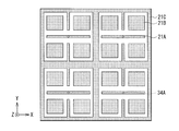
- FIG. 2 is a schematic plan view illustrating an example of a layout of a lower electrode included in the organic photoelectric conversion unit illustrated in FIG. 1.
- FIG. 5B is a perspective view showing the layout of the lower electrode shown in FIG. 5A.
- FIG. 5A is a perspective view showing the layout of the lower electrode shown in FIG. 5A.
- FIG. 2 is a schematic plan view illustrating another example of a layout of a lower electrode included in the organic photoelectric conversion unit illustrated in FIG. 1.
- FIG. 5B is a perspective view showing the layout of the lower electrode shown in FIG. 5A.
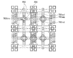
- FIG. 2 is a schematic plan view illustrating an example of a layout of one inorganic photoelectric conversion unit illustrated in FIG. 1 and various transistors related thereto.
- FIG. 2 is a schematic plan view illustrating an example of a layout of another inorganic photoelectric conversion unit illustrated in FIG. 1 and various transistors related thereto.
- FIG. 2 is a signal line layout diagram for driving a storage electrode shown in FIG. 1. It is a figure showing a part of wiring connected to an adjacent photoelectric conversion part and various transistors related to this.
- FIG. 2 is a cross-sectional view for describing a method for manufacturing the imaging device illustrated in FIG. 1.
- FIG. 14 is a schematic sectional view illustrating a step following FIG. 13.
- FIG. 15 is a schematic sectional view illustrating a step following FIG. 14.
- FIG. 16 is a schematic sectional view illustrating a step following FIG. 15.
- FIG. 2 is a timing chart illustrating an operation example of the imaging device illustrated in FIG. 1.
- FIG. 9 is a schematic cross-sectional view illustrating a configuration of a main part of an imaging element according to a second embodiment of the present disclosure.
- FIG. 14 is a schematic cross-sectional view illustrating a configuration of a main part of an imaging element according to a third embodiment of the present disclosure.
- FIG. 14 is a schematic cross-sectional view illustrating a configuration of a main part of an image sensor according to a fourth embodiment of the present disclosure.
- FIG. 11 is a schematic plan view illustrating another example of a layout of a lower electrode included in an organic photoelectric conversion unit according to a modified example of the present disclosure.
- FIG. 11 is a schematic plan view illustrating another example of a layout of one inorganic photoelectric conversion unit and various transistors related thereto according to a modified example of the present disclosure.
- FIG. 11 is a schematic plan view illustrating another example of a layout of another inorganic photoelectric conversion unit according to a modified example of the present disclosure and various transistors related thereto.
- FIG. 11 is a diagram illustrating another example of a wiring connected to a photoelectric conversion unit and various transistors related thereto according to a modification example of the present disclosure.
- FIG. 11 is a diagram illustrating another example of a wiring connected to a photoelectric conversion unit and various transistors related thereto according to a modification example of the present disclosure.
- FIG. 11 is a schematic plan view illustrating another example of a layout of one inorganic photoelectric conversion unit and various transistors related thereto according to a modified example of the present disclosure.
- FIG. 11 is a schematic plan view illustrating another example of a layout of another inorganic photoelectric conversion unit according to a
- FIG. 11 is a diagram illustrating another example of a wiring connected to a photoelectric conversion unit and various transistors related thereto according to a modification example of the present disclosure.
- FIG. 11 is a diagram illustrating another example of a wiring connected to a photoelectric conversion unit and various transistors related thereto according to a modification example of the present disclosure.
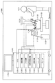
- FIG. 2 is a block diagram illustrating a configuration of an imaging device using the imaging device illustrated in FIG. 1 and the like as pixels.
- FIG. 29 is a functional block diagram illustrating an example of an electronic apparatus (camera) using the imaging device illustrated in FIG. 28. It is a block diagram which shows an example of a schematic structure of an in-vivo information acquisition system. It is a figure showing an example of the schematic structure of an endoscope operation system.
- FIG. 1 is a block diagram illustrating another example of a wiring connected to a photoelectric conversion unit and various transistors related thereto according to a modification example of the present disclosure.
- FIG. 2 is a block diagram illustrating a
- FIG. 3 is a block diagram illustrating an example of a functional configuration of a camera head and a CCU. It is a block diagram showing an example of a schematic structure of a vehicle control system. It is explanatory drawing which shows an example of the installation position of a vehicle exterior information detection part and an imaging part.
- Third embodiment an example in which a first hydrogen block layer and a second hydrogen block layer are directly stacked in a peripheral region
- Fourth embodiment an example in which an insulating layer on a lower electrode is formed as a second hydrogen block layer
- Modified example other example of pixel layout
- Application example 7 Application examples
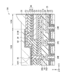
- FIG. 1 illustrates a cross-sectional configuration of an imaging device (imaging device 10A) according to the first embodiment of the present disclosure.
- FIG. 2 illustrates a cross-sectional configuration of a main part of the image sensor 10A illustrated in FIG.
- FIG. 3 is an equivalent circuit diagram of the image sensor 10A shown in FIG.
- FIG. 4 schematically shows the arrangement of the lower electrode 21 of the image sensor 10 and the transistors constituting the control unit shown in FIG.
- the image pickup device 10A is, for example, a single pixel (unit pixel P) in an image pickup device (image pickup device 1; see FIG. 28) such as a CMOS (Complementary Metal Oxide Semiconductor) image sensor used for electronic devices such as digital still cameras and video cameras.
- CMOS Complementary Metal Oxide Semiconductor
- the imaging device 1 has an effective pixel area 110A in which a plurality of pixels are arranged, and a peripheral area 110B provided around the effective pixel area 110A and in which peripheral circuits such as the row scanning unit 131 are formed.
- An image sensor 10A is formed in each of the plurality of pixels.
- the image pickup device 10A of the present embodiment is one in which the organic photoelectric conversion unit 20 is provided on the light receiving surface (first surface; surface 30S1) of the semiconductor substrate 30, and the organic photoelectric conversion unit 20 is arranged from the semiconductor substrate 30 side.
- a lower electrode 21 (first electrode) composed of a plurality of electrodes, an insulating layer 22, a charge storage layer 23, a photoelectric conversion layer 24 (organic photoelectric conversion layer), and an upper electrode 25 (second electrode) laminated in this order.
- the stacked charge accumulation layer 23 and photoelectric conversion layer 24 are formed to extend in the effective pixel region 110A as a common layer for a plurality of pixels provided in the effective pixel region 110A.
- the image sensor 10A has a pixel sharing structure in which four adjacent pixels share one corresponding floating diffusion FD1, FD2, or FD3.
- the imaging device 10A is, for example, a so-called vertical spectral imaging device in which one organic photoelectric conversion unit 20 and two inorganic photoelectric conversion units 32B and 32R are vertically stacked.
- the organic photoelectric conversion unit 20 is provided on the first surface (back surface; surface 30S1) side of the semiconductor substrate 30 as described above.
- the inorganic photoelectric conversion units 32B and 32R are embedded in the semiconductor substrate 30 and stacked in the thickness direction of the semiconductor substrate 30.
- the organic photoelectric conversion unit 20 has a charge storage layer 23 and a photoelectric conversion layer 24 between a lower electrode 21 and an upper electrode 25 which are arranged opposite to each other, as will be described in detail later.
- the insulating layer 22 is provided between the two.
- the lower electrode 21 is composed of a plurality of electrodes (readout electrode 21A, storage electrode 21B, and shield electrode 21C).
- the read electrode 21A is electrically connected to the charge storage layer 23 through an opening 22H formed in the insulating layer 22.
- the photoelectric conversion layer 24 includes a p-type semiconductor and an n-type semiconductor, and has a bulk heterojunction structure in the layer.
- the bulk heterojunction structure is a p / n junction surface formed by mixing a p-type semiconductor and an n-type semiconductor.
- the organic photoelectric conversion unit 20 and the inorganic photoelectric conversion units 32B and 32R perform photoelectric conversion by selectively detecting light in different wavelength ranges. Specifically, for example, the organic photoelectric conversion unit 20 acquires a green (G) color signal.
- the inorganic photoelectric conversion units 32B and 32R acquire blue (B) and red (R) color signals, respectively, depending on the difference in the absorption coefficient. Thereby, in the image sensor 10A, a plurality of types of color signals can be obtained in one pixel without using a color filter.
- this embodiment mode describes a case where electrons are read out as signal charges from an electron-hole pair (electron-hole pair) generated by photoelectric conversion (a case where an n-type semiconductor region is used as a photoelectric conversion layer). I do.
- “+ (plus)” added to “p” and “n” indicates that the p-type or n-type impurity concentration is high.
- the semiconductor substrate 30 On the second surface (front surface; 30S2) of the semiconductor substrate 30, for example, a floating diffusion (floating diffusion layer) FD1 (region 35 in the semiconductor substrate 30), FD2, FD3, transfer transistors TR2trs, TR3trs, and an amplifier transistor ( (Modulation elements) TR1amp and TR2amp, reset transistors TR1rst and TR2rst, select transistors TR1sel and TR2sel, and a multilayer wiring 40.
- the multilayer wiring 40 has, for example, a configuration in which wiring layers 41, 42, and 43 are stacked in an insulating layer 44.
- the first surface (surface 30S1) side of the semiconductor substrate 30 is referred to as a light incident side S1
- the second surface (surface 30S2) side is referred to as a wiring layer side S2.
- the organic photoelectric conversion unit 20 is configured such that the lower electrode 21, the insulating layer 22, the charge storage layer 23, the photoelectric conversion layer 24, and the upper electrode 25 are formed from the first surface (the surface 30S1) of the semiconductor substrate 30. It has a configuration stacked in this order.
- the lower electrode 21 is formed, for example, separately from the readout electrode 21A and the storage electrode 21B separated from each other with the insulating layer 22 interposed therebetween and the shield electrode 21C surrounding four pixels adjacent to each other, while being formed separately for each imaging element 10A. It is configured.
- the readout electrode 21A is shared by two or four pixels adjacent to each other and has an opening 22H provided in the insulating layer 22, as shown in FIGS. 5A and 6A, for example.
- the charge storage layer 23, the photoelectric conversion layer 24, and the upper electrode 25 are provided as a continuous layer common to the plurality of imaging elements 10A, and extend to the effective pixel region 110A.
- a hydrogen block layer 26 is further provided on the upper electrode 25. The hydrogen block layer 26 is stacked on the insulating layer 22 from above the upper electrode 25 via the side surfaces of the upper electrode 25, the photoelectric conversion layer 24, and the charge storage layer 23, for example, in the peripheral region 110B.
- a fixed charge layer 27 Between the first surface (surface 30S1) of the semiconductor substrate 30 and the lower electrode 21, for example, a fixed charge layer 27, an insulating layer 28, and an interlayer insulating layer 29 are provided in this order.
- a first protective layer 51, a second protective layer 53, and an on-chip lens layer 56 are provided in this order.
- the wiring 52 is provided between the first protective layer 51 and the second protective layer 53, and the light shielding film 54 is provided between the second protective layer 53 and the on-chip lens layer 56.
- Through electrodes 34A, 34B, 34C, 34D are provided between the first surface (surface 30S1) and the second surface (surface 30S2) of the semiconductor substrate 30.
- the through electrode 34A is electrically connected to the readout electrode 21A of the organic photoelectric conversion unit 20, and the organic photoelectric conversion unit 20 is connected via the through electrode 34 to, for example, the gate Gamp of the amplifier transistor TR1amp and the floating diffusion FD1.
- the penetrating electrode 34B is electrically connected to the storage electrode 21B of the organic photoelectric conversion unit 20, so that a voltage can be applied to the storage electrode 21B independently of the readout electrode 21A.
- the through-electrode 34C is electrically connected to the shield electrode 21C, thereby suppressing charge leakage to an adjacent pixel.
- the through electrode 34D is electrically connected to the pad 36D provided in the peripheral region 110B.
- the wiring 52 is electrically connected to the pad portion 36D via the opening 51H1, and forms a guard ring 55.
- a voltage can be applied to the upper electrode 25.
- the guard ring 55 can prevent water from entering from the outer periphery.
- the wiring 52 forming the guard ring 55 does not necessarily need to be electrically connected to the upper electrode 25.
- FIG. 2 shows an example in which the second protective layer 53 is embedded in the opening 51H1 forming the guard ring 55.
- the present invention is not limited to this.
- the hydrogen blocking layer 26 and the first protective layer 51 are embedded. May be.
- the lower ends of the through electrodes 34A, 34B, 34C, 34D are connected to the wiring layer 41, respectively.
- the through electrode 34A is connected to the connection portion 41A in the wiring layer 41, and the connection portion 41A and the floating diffusion FD1 (region 35) are connected, for example, via the lower first contact 45.
- the upper end of the through electrode 34A is connected to the readout electrode 21A via, for example, a pad 35A, a via V2, a pad 36A, and a via V1.
- the through-electrode 34A is provided, for example, one for each of four pixels adjacent to each other.
- the through electrode 34A has a function as a connector between the organic photoelectric conversion unit 20 of each pixel and the gate Gamp of the amplifier transistor TR1amp and the floating diffusion FD1, and at the same time, a charge (here, electrons) generated in the organic photoelectric conversion unit 20. It is a transmission path.
- the reset gate Grst of the reset transistor TR1rst is arranged next to the floating diffusion FD1 (one source / drain region of the reset transistor TR1rst). This makes it possible to reset the charge accumulated in the floating diffusion FD1 by the reset transistor TR1rst.
- the imaging device 10A of the present embodiment light incident on the organic photoelectric conversion section 20 from the upper electrode 25 side is absorbed by the photoelectric conversion layer 24.
- the excitons thus generated move to the interface between the electron donor and the electron acceptor constituting the photoelectric conversion layer 24, and exciton separation, that is, dissociation into electrons and holes.
- the charges (electrons and holes) generated here are diffused due to a difference in carrier concentration or due to an internal electric field due to a difference in work function between an anode (here, the upper electrode 25) and a cathode (here, the lower electrode 21). Each is carried to a different electrode and detected as a photocurrent. Further, by applying a potential between the lower electrode 21 and the upper electrode 25, the transport direction of electrons and holes can be controlled.
- the organic photoelectric conversion unit 20 absorbs green light corresponding to part or all of a selective wavelength range (for example, 450 nm or more and 650 nm or less) to generate an electron-hole pair. It is.
- a selective wavelength range for example, 450 nm or more and 650 nm or less
- the lower electrode 21 is composed of the readout electrode 21A, the storage electrode 21B, and the shield electrode 21C which are formed separately as described above.
- the readout electrode 21A is for transferring electric charges (here, electrons) generated in the photoelectric conversion layer 24 to the floating diffusion FD1, and includes, for example, a via V1, a pad portion 36A, a via V2, a pad portion 35A, a penetrating portion. It is connected to the floating diffusion FD1 via the electrode 34, the connecting portion 41A and the lower first contact 45.
- the storage electrode 21 ⁇ / b> B is for storing electrons in the charge storage layer 23 as signal charges among charges generated in the photoelectric conversion layer 24.
- the storage electrode 21B is provided in a region that covers the light receiving surfaces of the inorganic photoelectric conversion units 32B and 32R formed in the semiconductor substrate 30 and faces these light receiving surfaces.
- the storage electrode 21B is preferably larger than the readout electrode 21A, so that a large amount of charges can be stored.
- the shield electrode 21C is for suppressing charge leakage to the adjacent pixel.
- the lower electrode 21 is made of a light-transmitting conductive film, and is made of, for example, ITO (indium tin oxide).
- ITO indium tin oxide
- a tin oxide (SnO 2 ) -based material to which a dopant is added or a zinc oxide-based material obtained by adding a dopant to zinc oxide (ZnO) is used. May be used.
- the zinc oxide-based material include aluminum zinc oxide (AZO) to which aluminum (Al) is added as a dopant, gallium zinc oxide (GZO) to which gallium (Ga) is added, and indium zinc oxide to which indium (In) is added. (IZO).
- the thickness of the lower electrode 21 is preferably, for example, 20 nm to 200 nm, and more preferably 30 nm or more and 100 nm or less.
- the insulating layer 22 is for electrically insulating the storage electrode 21B from the charge storage layer 23.
- the insulating layer 22 is provided, for example, on the interlayer insulating layer 29 and the lower electrode 21 so as to cover the lower electrode 21.
- an opening 22H is provided on the reading electrode 21A among the lower electrodes 21, and the reading electrode 21A and the charge storage layer 23 are electrically connected through the opening 22H.
- the insulating layer 22 is, for example, a single-layer film made of one of silicon oxide (SiO x ), silicon nitride (SiN x ), silicon oxynitride (SiO x N y ), and the like, or a single layer film thereof. It is composed of two or more kinds of laminated films.
- the thickness of the insulating layer 22 is, for example, 20 nm to 500 nm.
- the charge storage layer 23 is provided below the photoelectric conversion layer 24, specifically, between the insulating layer 22 and the photoelectric conversion layer 24, and stores signal charges (here, electrons) generated in the photoelectric conversion layer 24. It is for doing.
- the charge storage layer 23 is preferably formed using a material having a higher charge mobility and a larger band gap than the photoelectric conversion layer 24.
- the band gap of the constituent material of the charge storage layer 23 is preferably 3.0 eV or more.
- examples of such a material include an oxide semiconductor material such as IGZO and an organic semiconductor material.
- the organic semiconductor material include transition metal dichalcogenide, silicon carbide, diamond, graphene, carbon nanotube, condensed polycyclic hydrocarbon compound, condensed heterocyclic compound, and the like.
- the thickness of the charge storage layer 23 is, for example, not less than 10 nm and not more than 300 nm.
- the photoelectric conversion layer 24 converts light energy into electric energy.
- the photoelectric conversion layer 24 includes, for example, two or more types of organic materials (p-type semiconductor materials or n-type semiconductor materials) each functioning as a p-type semiconductor or an n-type semiconductor.
- the photoelectric conversion layer 24 has a bonding surface (p / n bonding surface) between the p-type semiconductor material and the n-type semiconductor material in the layer.
- the p-type semiconductor relatively functions as an electron donor (donor), and the n-type semiconductor relatively functions as an electron acceptor (acceptor).
- the photoelectric conversion layer 24 provides a field where excitons generated when light is absorbed are separated into electrons and holes, and specifically, an interface (p / p) between an electron donor and an electron acceptor. At the (n-junction surface), the exciton separates into electrons and holes.
- the photoelectric conversion layer 24 includes, in addition to the p-type semiconductor material and the n-type semiconductor material, an organic material that photoelectrically converts light in a predetermined wavelength band and transmits light in another wavelength band, a so-called dye material. It may be. In the case where the photoelectric conversion layer 24 is formed using three types of organic materials, a p-type semiconductor material, an n-type semiconductor material, and a dye material, the p-type semiconductor material and the n-type semiconductor material are in a visible region (for example, 450 nm to (800 nm). The thickness of the photoelectric conversion layer 24 is, for example, 50 nm to 500 nm.
- Examples of the organic material constituting the photoelectric conversion layer 24 include quinacridone, chlorinated boron subphthalocyanine, pentacene, benzothienobenzothiophene, fullerene, and derivatives thereof.
- the photoelectric conversion layer 24 is configured by combining two or more of the above organic materials.
- the organic material functions as a p-type semiconductor or an n-type semiconductor depending on the combination.
- the organic material forming the photoelectric conversion layer 24 is not particularly limited. In addition to the organic materials described above, for example, any one of naphthalene, anthracene, phenanthrene, tetracene, pyrene, perylene, and fluoranthene or a derivative thereof is preferably used. Alternatively, polymers such as phenylenevinylene, fluorene, carbazole, indole, pyrene, pyrrole, picoline, thiophene, acetylene, and diacetylene, and derivatives thereof may be used.
- metal complex dyes cyanine dyes, merocyanine dyes, phenylxanthene dyes, triphenylmethane dyes, rhodacyanine dyes, xanthene dyes, macrocyclic azaannulene dyes, azulene dyes, naphthoquinones, anthraquinone dyes, Condensed polycyclic aromatic and aromatic or heterocyclic compounds such as anthracene and pyrene, or a chain compound condensed with two or more quinoline, benzothiazole, benzoxazole, etc.
- a nitrogen heterocycle, or a cyanine-like dye linked by a squarylium group and a croconite methine group can be preferably used.
- the metal complex dye is preferably a dithiol metal complex dye, a metal phthalocyanine dye, a metal porphyrin dye, or a ruthenium complex dye, but is not limited thereto.
- a charge storage layer 23 an electron blocking film, a photoelectric conversion layer 24, a hole blocking film, a work function adjusting layer, and the like may be stacked in this order from the lower electrode 21 side.
- an undercoat layer and a hole transport layer may be provided between the lower electrode 21 and the photoelectric conversion layer 24, and a buffer layer and an electron transport layer may be provided between the photoelectric conversion layer 24 and the upper electrode 25.
- the upper electrode 25 is made of a conductive film having optical transparency, like the lower electrode 21. In the imaging device 1 using the imaging element 10A as one pixel, the upper electrode 25 may be separated for each pixel, or may be formed as a common electrode for each pixel. The thickness of the upper electrode 25 is, for example, 10 nm to 200 nm. As shown in FIG. 2, a wiring 52 is electrically connected to the upper electrode 25 via, for example, an opening 51H2. The wiring 52 is also electrically connected to the pad portion 36D through the opening 51H1, as shown in FIG. That is, the upper electrode 25 is electrically connected to the pad portion 36D via the wiring 52, for example.
- the hydrogen blocking layer 26 is for suppressing the intrusion of hydrogen (H 2 ) into the charge storage layer 23.
- the hydrogen blocking layer 26 is provided on the upper electrode 25 in the effective pixel region 110A, and is provided on the peripheral region 110B.
- the insulating layer 22 is stacked on the insulating layer 22 from the upper surface of the upper electrode 25 via the side surfaces of the upper electrode 25, the photoelectric conversion layer 24, and the charge storage layer 23, and is formed to extend, for example, to the end of the peripheral region 110B.
- Examples of the material forming the hydrogen blocking layer 26 include an insulating material. Specifically, it is preferable to use a material having a light-transmitting property and a high sealing property.
- Examples of such a material include a metal oxide such as aluminum oxide (AlO x ) and silicon nitride (SiN x). ), Carbon-containing silicon oxide (SiOC), and the like.
- a metal oxide such as aluminum oxide (AlO x ) and silicon nitride (SiN x).
- SiOC Carbon-containing silicon oxide
- an oxide semiconductor such as ITO (indium tin oxide) may be used.
- the hydrogen blocking layer 26 has, for example, a lower hydrogen content than the insulating layer 22 or the film itself does not contain hydrogen. Further, it is preferable that the hydrogen blocking layer 26 has a small stress and further has an ultraviolet absorbing ability. Furthermore, it is preferable to form a film containing a small amount of water and to suppress the intrusion of water (H 2 O).
- the hydrogen blocking layer 26 is formed of a single-layer film formed using the above-described material or a laminated film including two or more of the above-described materials.
- the thickness of the hydrogen blocking layer 26 is, for example, not less than 10 nm and not more than 1000 nm.
- the fixed charge layer 27 may be a film having a positive fixed charge or a film having a negative fixed charge.
- Materials for the film having a negative fixed charge include hafnium oxide (HfO x ), aluminum oxide (AlO x ), zirconium oxide (ZrO x ), tantalum oxide (TaO x ), titanium oxide (TiO x ), and lanthanum oxide ( LaO x ), praseodymium oxide (PrO x ), cerium oxide (CeO x ), neodymium oxide (NdO x ), promethium oxide (PmO x ), samarium oxide (SmO x ), europium oxide (EuO x ), gadolinium oxide (GdO) x), terbium oxide (TBO x), dysprosium oxide (DyO x), holmium oxide (HoO x), thulium oxide (TMO x), ytterb
- the fixed charge layer 27 may have a configuration in which two or more types of films are stacked. Thereby, for example, in the case of a film having a negative fixed charge, the function as a hole accumulation layer can be further enhanced.
- the insulating layer 28 is formed on the fixed charge layer 27 formed on the first surface (the surface 30S1) of the semiconductor substrate 30 and in the through holes 30H1, 30H2, 30H3, and 30H4 in which the through electrodes 34A, 34B, 34C, and 34D are formed. It is provided between the fixed charge layer 27 and the through electrodes 34A, 34B, 34C, 34D, and is for electrically insulating the through electrode 34 and the semiconductor substrate 30 from each other.
- the material of the insulating layer 28 is not particularly limited.
- the insulating layer 28 is formed of silicon oxide (SiO x ), TEOS, silicon nitride (SiN x ), silicon oxynitride (SiO x N y ), or the like.
- the interlayer insulating layer 29 is a single layer made of, for example, one of silicon oxide (SiO x ), TEOS, silicon nitride (SiN x ), silicon oxynitride (SiO x N y ), and the like. It is composed of a film or a laminated film composed of two or more of these.
- pad portions 35C and 36C for electrically connecting the shield electrode 21C and the through electrode 34C, pad portions 35D and 36D for electrically connecting the wiring 52 and the through electrode 34D, and electrically connecting each electrode and the pad portion.
- the first protection layer 51 and the second protection layer 53 are provided on the entire surface of the semiconductor substrate 30 including the effective pixel region 110A and the peripheral region 110B, for example. It is preferable that the first protective layer 51 and the second protective layer 53 are formed using, for example, a material having a light-transmitting property and a high sealing property. Examples of such a material include insulating materials such as aluminum oxide (AlO x ), silicon nitride (SiN x ), and carbon-containing silicon oxide (SiOC).
- the first protective layer 51 and the second protective layer 53 preferably have a lower hydrogen content than the insulating layer 22, for example, as in the case of the hydrogen blocking layer 26, or the films themselves do not contain hydrogen.
- first protective layer 51 and the second protective layer 53 have a small stress and further have an ultraviolet absorbing ability. Furthermore, it is preferable that the first protective layer 51 and the second protective layer 53 contain a small amount of water, and it is preferable to suppress intrusion of water (H 2 O). From the above, it is preferable to use aluminum oxide (AlO x ) among the above materials as the material of the first protective layer 51 and the second protective layer 53.
- AlO x aluminum oxide
- the first protective layer 51 and the second protective layer 53 may be formed using the same material as that of the insulating layer 28 and the interlayer insulating layer 29.
- the first protective layer 51 and the second protective layer 53 are single-layer films made of one of silicon oxide (SiO x ), silicon nitride (SiN x ), silicon oxynitride (SiO x N y ), and the like. Or two or more of aluminum oxide (AlO x ), silicon nitride (SiN x ), carbon-containing silicon oxide film (SiOC), silicon oxide (SiO x ), and silicon oxynitride (SiO x N y ) It may be a laminated film.
- the thickness of the first protective layer 51 is, for example, 100 nm to 1000 nm.
- the thickness of the second protective layer 53 is, for example, 10 nm to 1000 nm.
- the wiring 52 is provided on the second protective layer 53 in the peripheral region 110B. As described above, the wiring 52 is electrically connected to the upper electrode 25 via the opening 51H2 penetrating the first protective layer 51 and the hydrogen block layer 26, for example.
- the wiring 52 is electrically connected to the pad portion 36D provided in the interlayer insulating layer 29 through the opening 51H1 penetrating through the first protective layer 51, the hydrogen blocking layer 26, and the insulating layer 22 in the peripheral region 110B.
- a guard ring 55 is formed.
- the pad portion 36D is connected to a through electrode 34D that penetrates the via V2, the pad portion 35D, and the semiconductor substrate 30 and is connected to the wiring layer 41 provided on the second surface (surface 30S2) side of the semiconductor substrate 30. Thereby, it functions as a transmission path for charges (here, holes) generated in the organic photoelectric conversion unit 20.
- the light-shielding film 54 is provided on the second protective layer 53 in the peripheral region 110B.
- Examples of the material of the light-shielding film 54 include tungsten (W), titanium (Ti), titanium nitride (TiN), and aluminum (Al).
- the light-shielding film 54 is, for example, a laminated film of W / TiN / Ti or W As a single-layer film.
- the thickness of the light shielding film 54 is, for example, not less than 50 nm and not more than 400 nm.
- an on-chip lens layer 56 in which the on-chip lens 56L (microlens) is formed for each unit pixel P in the effective pixel region 110A is provided.
- the on-chip lens 56L collects light incident from above onto the respective light receiving surfaces of the organic photoelectric conversion unit 20, the inorganic photoelectric conversion unit 32B, and the inorganic photoelectric conversion unit 32R.
- an optical member such as a color filter for controlling the spectral distribution may be provided below the on-chip lens 56L.
- the semiconductor substrate 30 is formed of, for example, an n-type silicon (Si) substrate, and has a p-well 31 in a predetermined region (for example, the pixel unit 1a).
- the transfer transistor TR1trs, TR2trs, TR3trs, the amplifier transistors TR1amp, TR2amp, the reset transistors TR1rst, TR2rst, the selection transistors TR1sel, TR2sel, and the like are provided on the second surface (the surface 30S2) of the p-well 31.
- a pixel readout circuit, a pixel drive circuit, and the like, which are formed by a logic circuit, are provided in the peripheral region 110B of the semiconductor substrate 30, for example.
- FIG. 5A illustrates an example of a layout of the lower electrode 21 included in the organic photoelectric conversion unit 20, and FIG. 5B illustrates a layout of the lower electrode 21 illustrated in FIG. 5A as a transparent perspective view.
- 6A illustrates an example of a layout of the lower electrode 21 included in the organic photoelectric conversion unit 20, and FIG. 6B illustrates a layout of the lower electrode 21 illustrated in FIG. 6A as a transparent perspective view.
- FIG. 7 illustrates an example of a layout of the inorganic photoelectric conversion unit 32B and various transistors related thereto.
- FIG. 8 illustrates an example of a layout of the inorganic photoelectric conversion unit R and various transistors related thereto.
- FIG. 9 illustrates an example of signal wiring for driving the storage electrode 21 ⁇ / b> B in the organic photoelectric conversion unit 20.
- FIGS. 10 to 12 show an example of wiring connected to each of the photoelectric conversion units 20, 32B, 32R and various transistors related thereto.
- the organic photoelectric conversion unit 20 of the present embodiment four adjacent organic photoelectric conversion units 20 are connected to one floating diffusion FD1.
- One reset transistor TR1rst and a power supply line Vdd are connected in series to the floating diffusion FD1.
- one of the amplifier transistor TR1amp and one of the selection transistor TR1sel and a signal line (data output line) VSL1 are connected in series to the floating diffusion FD1.
- four storage electrodes 21B adjacent to each other and a reset transistor TR1rst, an amplifier transistor TR1amp, and a selection transistor TR1sel provided one for each pixel are adjacent to each other.
- a set of control units (first control units) responsible for the read operation and the reset operation of the four organic photoelectric conversion units 20 is configured.
- the first control unit is used, for example, to perform the reading process sequentially in a time-division manner.
- inorganic photoelectric conversion unit 32B of the present embodiment four photodiodes PD2 adjacent to each other are connected to one floating diffusion FD2 via four transfer transistors TR2trs provided one for each pixel. I have.
- inorganic photoelectric conversion unit 32R of the present embodiment similarly to the inorganic photoelectric conversion unit 32B, four photodiodes PD3 adjacent to each other are connected via four transfer transistors TR3trs provided one for each pixel. It is connected to one floating diffusion FD3.
- One reset transistor TR2rst and one power supply line Vdd are connected in series to one floating diffusion FD2. Apart from this, one of the amplifier transistor TR2amp and one of the selection transistor TR2sel and a signal line (data output line) VSL2 are connected in series to the floating diffusion FD2.
- the inorganic photoelectric conversion unit 32B and the inorganic photoelectric conversion unit 32R are provided with the transfer transistor TR2trs and the transfer transistor TR3trs provided for each pixel, and for each pixel.
- the reset transistor TR2rst, the amplifier transistor TR2amp, and the selection transistor TR2sel each of which is provided one by one, provide a set of control units (for a read operation and a reset operation of the four inorganic photoelectric conversion units 32B and 32R adjacent to each other).
- a second control unit That is, in the four inorganic photoelectric conversion units 32B and the four inorganic photoelectric conversion units 32R provided in the stacked imaging device 10A for four pixels, one set of the control unit (the second control unit) except the transfer transistors TR2trs and TR3trs. Part) is shared.
- the second control unit When reading out the signal charges from the floating diffusion FD2 corresponding to the four inorganic photoelectric conversion units 32B adjacent to each other and the floating diffusion FD3 corresponding to the four inorganic photoelectric conversion units 32R, the second control unit is used, for example. The reading process is performed sequentially in time division.
- the floating diffusions FD2 and FD3 which are shared by the four inorganic photoelectric conversion units 32B and 32R adjacent to each other, are arranged at locations separated by one pixel each. This makes it possible to achieve high integration of the imaging element 10A.
- the image sensor 10A of the present embodiment can be manufactured, for example, as follows.
- a p-well 31 is formed as a well of a first conductivity type in a semiconductor substrate 30, and inorganic photoelectric conversion units 32 B and 32 R of a second conductivity type (for example, n-type) are formed in the p-well 31. I do.
- a p + region is formed near the first surface (surface 30S1) of the semiconductor substrate 30.
- a gate insulating layer 33 On the second surface (surface 30S2) of the semiconductor substrate 30, for example, after forming n + regions serving as floating diffusions FD1 to FD3, a gate insulating layer 33, various transfer transistors TR1trs, TR2trs, TR3trs, select transistors TR1sel, TR2sel, A gate wiring layer 47 including the gates of the amplifier transistors TR1amp and TR2amp and the reset transistors TR1rst and TR2rst is formed. Thus, various transfer transistors TR1trs, TR2trs, TR3trs, select transistors TR1sel, TR2sel, amplifier transistors TR1amp, TR2amp, and reset transistors TR1rst, TR2rst are formed. Further, on the second surface (surface 30S2) of the semiconductor substrate 30, the multilayer wiring 40 including the wiring layers 41 to 43 including the lower first contact 45 and the connection portion 41A and the insulating layer 44 is formed.
- an SOI (Silicon On Insulator) substrate in which the semiconductor substrate 30, a buried oxide film (not shown), and a holding substrate (not shown) are laminated is used as the base of the semiconductor substrate 30.
- the buried oxide film and the holding substrate are joined to the first surface (surface 30S1) of the semiconductor substrate 30. After the ion implantation, an annealing process is performed.
- a support substrate (not shown) or another semiconductor substrate is bonded to the second surface (surface 30S2) side (multilayer wiring 40 side) of the semiconductor substrate 30, and the semiconductor substrate 30 is turned upside down.
- the semiconductor substrate 30 is separated from the buried oxide film of the SOI substrate and the holding substrate, and the first surface (the surface 30S1) of the semiconductor substrate 30 is exposed.
- the above steps can be performed by a technique used in a normal CMOS process such as ion implantation and CVD (Chemical Vapor Deposition).
- the semiconductor substrate 30 is processed from the first surface (surface 30S1) side by, for example, dry etching to form, for example, annular through holes 30H1, 30H2, 30H3, and 30H4.
- the depth of the through holes 30H1 to 30H4 penetrates from the first surface (the surface 30S1) to the second surface (the surface 30S2) of the semiconductor substrate 30.
- the fixed charge layer 27 is formed on the first surface (the surface 30S1) and the side surface of the through hole 30H of the semiconductor substrate 30 by using, for example, an atomic layer deposition (ALD) method.
- ALD atomic layer deposition
- the fixed charge layer 27 that is continuous with the first surface (the surface 30S1) of the semiconductor substrate 30 and the side surfaces and the bottom surfaces of the through holes 30H1, 30H2, 30H3, and 30H4 is formed.
- the insulating layer 28 is formed on the first surface (the surface 30S1) of the semiconductor substrate 30 of the fixed charge layer 27 and in the through holes 30H1, 30H2, 30H3, and 30H4, an interlayer is further formed on the insulating layer 28.
- An insulating film for forming the insulating layer 29 is formed.
- the insulating film constituting the interlayer insulating layer 29, the insulating layer 28, the fixed charge layer 27, and the insulating layer 44 are formed.
- a through hole that penetrates and reaches the connection portion 41A is formed.
- the insulating film constituting the interlayer insulating layer 29 on the first surface (the surface 30S1) is also reduced in thickness.
- a photoresist PR is formed at a predetermined position on the conductive film.
- electrodes 34A, 34B, 34C, 34D having pad portions 35A, 35B, 35C, 35D are formed on the first surface (surface 30S1) of the semiconductor substrate 30. You.
- a via V2, pad portions 36, 36B, 36C, 36D, and a via V1 are formed on the insulating film and the through electrodes 34A, 34B, 34C, 34D forming the interlayer insulating layer 29, respectively, and then the CMP (Chemical @ Mechanical). Polishing), the surface of the interlayer insulating layer 29 is flattened. Subsequently, after a conductive film is formed on the interlayer insulating layer 29, a photoresist PR is formed at a predetermined position of the conductive film. Thereafter, the readout electrode 21A, the storage electrode 21B, and the shield electrode 21C are formed by etching and removing the photoresist PR.
- an opening 22H is provided on the readout electrode 21A.
- the charge storage layer 23, the photoelectric conversion layer 24, and the upper electrode 25 are formed on the insulating layer 22.
- the charge storage layer 23 and other organic layers are formed using an organic material, it is desirable that the charge storage layer 23 and other organic layers be formed continuously in a vacuum process (in a consistent vacuum process).
- the method for forming the photoelectric conversion layer 24 is not necessarily limited to the method using the vacuum evaporation method, but may be another method, for example, a spin coating technique or a printing technique.
- an aluminum oxide (AlO x ) film 26B is formed as a hard mask on the effective pixel region 110A on the upper electrode 25 by, for example, a physical vapor deposition (PVD) method. It is formed with a thickness of, for example, 10 nm to 50 nm. Note that the film formation method is not limited to this, and for example, a CVD method or an ALD method may be used.
- Examples of the film forming method of the PVD method include EB (electron beam) evaporation method, various sputtering methods (magnetron sputtering method, RF-DC combined bias sputtering method, ECR sputtering method, facing target sputtering method, high frequency sputtering method) and the like. Is mentioned.
- EB electron beam
- various sputtering methods magnetotron sputtering method, RF-DC combined bias sputtering method, ECR sputtering method, facing target sputtering method, high frequency sputtering method
- the PVD / ALD method has excellent coverage.
- the deposition rate of the CVD / ALD method is significantly lower than that of the PVD method. Therefore, if the upper electrode 25 can be sufficiently covered by the PVD method, it is preferable to use the PVD method.
- the AlO x film 26B is patterned using, for example, a lithography method to form a hard mask.
- FIG. 14 described later shows an example in which the photoresist PR is removed, the following process may be performed with the resist remaining after patterning the AlO x film 26B.
- the charge storage layer 23, the photoelectric conversion layer 24, and the upper electrode 25 formed in the peripheral region 110B are etched.
- an AlO x film 26A is formed to a thickness of, for example, 50 nm to 1000 nm by using, for example, the PVD method.
- a hydrogen block layer 26 composed of the AlO x films 26A and 26B is formed.
- the AlO x film 26A may be formed by a CVD method or an ALD method similarly to the AlO x film 26B. For example, when the step of the charge storage layer 23, the photoelectric conversion layer 24, and the upper electrode 25 is large.
- the hydrogen blocking layer 26 composed of a laminated film may be formed by combining the PVD method and the CVD / ALD method.
- a photoresist PR is patterned on the first protective layer 51, and is electrically connected to the through electrode 34D in the peripheral region 110B.
- An opening 51H1 penetrating to the pad portion 36D is formed.
- an opening 51H2 penetrating to the upper electrode 25 is formed. Note that the order of forming the openings 51H1 and 51H2 is not limited to this, and for example, the openings 51H1 and 51H2 may be formed simultaneously.
- the imaging device 10A when light enters the organic photoelectric conversion unit 20 via the on-chip lens 56L, the light passes through the organic photoelectric conversion unit 20, the inorganic photoelectric conversion units 32B and 32R in this order, and in the passing process. Photoelectric conversion is performed for each of green, blue, and red light. Hereinafter, the signal acquisition operation of each color will be described.
- green light is selectively detected (absorbed) in the organic photoelectric conversion unit 20 and photoelectrically converted.
- the organic photoelectric conversion unit 20 is connected to the gate Gamp of the amplifier transistor AMP and the floating diffusion FD1 via the through electrode 34. Therefore, electrons of the electron-hole pairs generated in the organic photoelectric conversion unit 20 are extracted from the lower electrode 21 side and transferred to the second surface (surface 30S2) side of the semiconductor substrate 30 via the through electrode 34. , Are accumulated in the floating diffusion FD1. At the same time, the charge generated in the organic photoelectric conversion unit 20 is modulated into a voltage by the amplifier transistor AMP.
- the reset gate Grst of the reset transistor TR1rst is arranged next to the floating diffusion FD1. As a result, the electric charge accumulated in the floating diffusion FD1 is reset by the reset transistor TR1rst.
- the organic photoelectric conversion unit 20 is connected not only to the amplifier transistor TR1amp but also to the floating diffusion FD1 via the through electrode 34A, the charge accumulated in the floating diffusion FD1 can be easily reset by the reset transistor TR1rst. It is possible to do.
- FIG. 17 illustrates an operation example of the imaging element 10A.
- A shows the potential at the storage electrode 21B
- B shows the potential at the floating diffusion FD1 (readout electrode 21A)
- C shows the potential at the gate (Gsel) of the reset transistor TR1rst. It is.
- a voltage is individually applied to the readout electrode 21A and the storage electrode 21B.
- the driving circuit applies the potential V1 to the readout electrode 21A and applies the potential V2 to the storage electrode 21B.
- the potentials V1 and V2 are set to V2> V1.
- charges (here, electrons) generated by the photoelectric conversion are attracted to the storage electrode 21B and are stored in a region of the charge storage layer 23 facing the storage electrode 21B (a storage period).
- the potential of the region of the charge storage layer 23 facing the storage electrode 21B becomes a more negative value as the time of the photoelectric conversion elapses.
- the holes are sent from the upper electrode 25 to the drive circuit.
- a reset operation is performed in a later stage of the accumulation period. Specifically, at the timing t1, the scanning unit changes the voltage of the reset signal RST from a low level to a high level. As a result, in the unit pixel P, the reset transistor TR1rst is turned on. As a result, the voltage of the floating diffusion FD1 is set to the power supply voltage VDD, and the voltage of the floating diffusion FD1 is reset (reset period).
- the driving circuit applies the potential V3 to the readout electrode 21A, and applies the potential V4 to the storage electrode 21B.
- the potentials V3 and V4 are set to V3 ⁇ V4.
- the charges (here, electrons) stored in the region corresponding to the storage electrode 21B are read out from the readout electrode 21A to the floating diffusion FD1. That is, the charges accumulated in the charge accumulation layer 23 are read out to the control unit (transfer period).
- the drive circuit again applies the potential V1 to the read electrode 21A and applies the potential V2 to the storage electrode 21B.
- the charges (here, electrons) generated by the photoelectric conversion are attracted to the storage electrode 21B and are stored in the region of the photoelectric conversion layer 24 facing the storage electrode 21B (accumulation period).
- the inorganic photoelectric conversion unit 32R electrons corresponding to the incident red light are accumulated in the n region of the inorganic photoelectric conversion unit 32R, and the accumulated electrons are transferred to the floating diffusion FD3 by the transfer transistor TR3trs.
- an imaging device such as a CCD image sensor or a CMOS image sensor can extract an R / G / B signal from one pixel and does not require demosaic processing.
- a stacked image sensor that does not generate color is used.
- This stacked-type imaging device has a configuration in which an organic photoelectric conversion unit including an organic photoelectric conversion layer using an organic semiconductor material is stacked on a semiconductor substrate in which a photodiode is embedded and formed.
- the organic photoelectric conversion layer is disposed so as to oppose the organic photoelectric conversion unit as a stacked-type imaging device capable of completely depleting the charge storage unit of the organic photoelectric conversion unit.
- One of the pair of electrodes (a first electrode and a second electrode) (e.g., a first electrode) is separated from the first electrode, and the organic photoelectric conversion layer is interposed via an insulating layer.
- An image pickup device provided with a charge storage electrode arranged opposite to the above has been developed.
- the organic photoelectric conversion layer has a stacked structure of, for example, a lower semiconductor layer formed using an oxide semiconductor material and an upper photoelectric conversion layer formed using an organic semiconductor material. It is possible to prevent recombination of the charges accumulated in the photoelectric conversion layer and to increase transfer efficiency to the first electrode.
- the oxide semiconductor material included in the lower semiconductor layer is easily reduced by hydrogen, which may cause oxygen vacancies and reduce operation stability.
- the charge storage layer 23 formed in the effective pixel region 110A as a common layer for the plurality of unit pixels P provided in the effective pixel region 110A and extending therethrough.
- the hydrogen block layer 26 is provided above the photoelectric conversion layer 24, specifically, on the upper electrode 25 formed to extend to the effective pixel region 110A.
- This hydrogen block layer 26 is provided, for example, on the entire surface of the effective pixel region 110A and the peripheral region 110B, and covers the upper electrode 25, the photoelectric conversion layer 24, and the side surfaces of the charge storage layer 23 from the upper surface of the upper electrode 25.
- the region 110 ⁇ / b> B has a configuration in which, for example, the insulating layer 22 is directly stacked.
- the oxide semiconductor material when used for the lower semiconductor layer, the oxide semiconductor material is reduced by hydrogen and oxygen vacancies occur. As a result, there is a possibility that leakage current increases, or charge accumulation or transfer failure occurs.
- the lower semiconductor layer corresponds to the charge storage layer 23 of the present embodiment.
- the hydrogen block layer 26 is provided on the entire surface of the effective pixel region 110A and the peripheral region 110B, and the side surfaces of the upper electrode 25, the photoelectric conversion layer 24, and the charge storage layer 23 from the upper surface of the upper electrode 25. And in the peripheral region 110B, for example, directly laminated on the insulating layer 22. Thereby, intrusion of hydrogen (H 2 ) into the charge storage layer 23 is suppressed.
- the hydrogen block layer 26 that seals above the charge storage layer 23 and the photoelectric conversion layer 24 formed to extend to the effective pixel region 110A and the side surfaces thereof is provided. Therefore, intrusion of hydrogen into the charge storage layer 23 is suppressed. Therefore, the generation of oxygen defects in the charge storage layer 23 is reduced, and the operation stability is improved. That is, it is possible to improve the reliability of the imaging device 10A and the imaging device 1 including the same.
- the hydrogen blocking layer 26 is formed using a material capable of forming a film containing a small amount of moisture, in addition to containing a small amount of hydrogen. Intrusion of moisture (H 2 O) is suppressed, and deterioration of the photoelectric conversion layer 24 can be prevented.
- a first protective layer 51 and a second protective layer 53 are provided on the hydrogen block layer 26, and an opening 51H1 penetrating the first protective layer 51, the hydrogen block layer 26, and the insulating layer 22 is formed.
- the opening 51H2 penetrating the first protective layer 51 and the hydrogen block layer 26 is buried with, for example, the second protective layer 53. This suppresses intrusion of hydrogen and moisture into the charge storage layer 23 through the openings 51H1 and 51H2.
- penetration of moisture (H 2 O) into the photoelectric conversion layer 24 is suppressed, and deterioration of the photoelectric conversion layer 24 can be prevented. Therefore, It is possible to further improve the reliability of the imaging device 10A and the imaging device 1 including the same.
- FIG. 18 schematically illustrates a cross-sectional configuration of a main part of an imaging device (imaging device 10B) according to the second embodiment of the present disclosure.
- the imaging element 10B forms one pixel (unit pixel P) in the imaging device 1 such as a CMOS image sensor used for an electronic device such as a digital still camera or a video camera, for example. Is what you do.
- the image pickup device 10B of the present embodiment has a structure in which a hydrogen block layer 61 (second hydrogen block layer) is further provided on a lower layer of the lower electrode 21, for example, on the interlayer insulating layer 29.
- the hydrogen block layer 61 is provided on the interlayer insulating layer 29, for example, on the entire surface of the effective pixel region 110A and the peripheral region 110B, and hydrogen (H 2 ) from below the charge storage layer 23. This is for suppressing the intrusion of the air.
- a material forming the hydrogen blocking layer 61 include an insulating material. Specifically, it is preferable to use a material having a light transmitting property and a high sealing property. Examples of such a material include aluminum oxide (AlO x ), silicon nitride (SiN x ), and carbon-containing silicon. An oxide film (SiOC) and the like can be mentioned.
- the hydrogen blocking layer 61 has, for example, a smaller hydrogen content than the insulating layer 22 or the film itself does not contain hydrogen. Further, the hydrogen blocking layer 61 has a small stress. From the above, it is desirable to use aluminum oxide (AlO x ) among the above materials as the material of the hydrogen blocking layer 61.
- the thickness of the hydrogen blocking layer 61 is, for example, not less than 10 nm and not more than 1000 nm.
- hydrogen The block layer 61 was provided. This makes it possible to suppress the intrusion of hydrogen (H 2 ) from the lower electrode 21 into the charge storage layer 23. Therefore, it is possible to further improve the reliability of the imaging device 10B and the imaging device 1 including the same.
- the hydrogen block layer 61 provided below the lower electrode 21 is provided on the interlayer insulating layer 29 immediately below the lower electrode 21; however, the present invention is not limited to this.
- the hydrogen block layer 61 only needs to be provided between the semiconductor substrate 30 and the lower electrode 21, and may be formed in the interlayer insulating layer 29, for example.
- FIG. 19 schematically illustrates a cross-sectional configuration of a main part of an image sensor (image sensor 10C) according to the third embodiment of the present disclosure.
- the imaging element 10C forms one pixel (unit pixel P) in the imaging device 1 such as a CMOS image sensor used for an electronic device such as a digital still camera and a video camera. Is what you do.
- An image sensor 10C of the present embodiment electrically insulates between the lower electrode 21 and the charge storage layer 23 in place of the insulating layer 22 of the second embodiment, and has, for example, An insulating layer 62 having the same side surface as the charge storage layer 23, the photoelectric conversion layer 24, and the upper electrode 25 is provided.
- the insulating layer 62 is for electrically insulating the storage electrode 21 ⁇ / b> B and the shield electrode 21 ⁇ / b> C from the charge storage layer 23, similarly to the insulating layer 22.
- the insulating layer 62 is provided, for example, on the interlayer insulating layer 29 and the lower electrode 21 so as to cover the lower electrode 21.
- the insulating layer 62 is provided with an opening on the readout electrode 21A of the lower electrode 21 in the same manner as the above-described insulating layer 22.
- the charge storage layer 23 is electrically connected.
- the insulating layer 62 is, for example, a single layer film made of one of silicon oxide (SiO x ), silicon nitride (SiN x ), silicon oxynitride (SiO x N y ), or aluminum oxide (AlO x ) Alternatively, a stacked film made of two or more of silicon nitride (SiN x ), carbon-containing silicon oxide (SiOC), silicon oxide (SiO x ), and silicon oxynitride (SiO x N y ) may be used.
- the thickness of the insulating layer 62 is, for example, 20 nm to 500 nm.
- the storage electrode 21B and the shield electrode 21C are electrically insulated from the charge storage layer 23, and the charge storage layer 23, the photoelectric conversion layer 24, and the upper electrode 25 are formed in the peripheral region 110B.
- An insulating layer 62 having the same side was formed. Accordingly, as described above, when the AlO x film is formed by using, for example, the ALD method, the upper electrode 25, the photoelectric conversion layer 24, the side surfaces of the charge storage layer 23 and the insulating layer 62, and the upper surface of the interlayer insulating layer 29 An AlO x film is formed on the hydrogen block layer 61 formed in the above.
- the hydrogen block layer 26 and the hydrogen block layer 61 are directly stacked in the peripheral region 110B. Therefore, since the organic photoelectric conversion unit 20 including the charge storage layer 23 is sealed by the hydrogen block layer 26 and the hydrogen block layer 61, the imaging of the first embodiment and the second embodiment is performed. It is possible to further suppress the intrusion of hydrogen (H 2 ) into the charge storage layer 23 as compared with the elements 10A and 10B, and it is possible to further improve the reliability of the imaging element 10C and the imaging device 1 including the same. Becomes
- FIG. 20 schematically illustrates a cross-sectional configuration of a main part of an imaging element (imaging element 10D) according to the fourth embodiment of the present disclosure.
- the image sensor 10D forms one pixel (unit pixel P) in an image pickup device 1 such as a CMOS image sensor used for an electronic device such as a digital still camera and a video camera, as in the first embodiment. Is what you do.
- the imaging device 10D of the present embodiment is the same as the hydrogen blocking layer 26 and the hydrogen blocking layer 61 as an insulating layer that electrically insulates between the lower electrode 21 and the charge storage layer 23 in the first embodiment. Is provided with an insulating layer 72 using the above material.
- the insulating layer 72 electrically insulates the storage electrode 21B and the shield electrode 21C from the charge storage layer 23, and prevents entry of hydrogen (H 2 ) from below the charge storage layer 23. It is for suppressing.
- the material As a material for forming the insulating layer 72, it is preferable that the material has light transmittance and high sealing property, similarly to the hydrogen block layer 26 and the hydrogen block layer 61. Further, a dense film with few defects is preferable. Such a material includes, for example, aluminum oxide (AlO x ).
- the insulating layer 72 for electrically insulating the storage electrode 21B and the shield electrode 21C from the charge storage layer 23 is formed using, for example, aluminum oxide (AlO x ). Therefore, the function as a hydrogen blocking layer is added to the insulating layer 72, and it is possible to suppress intrusion of hydrogen (H 2 ) from below the charge storage layer 23. Therefore, it is possible to further suppress the intrusion of hydrogen (H 2 ) into the charge storage layer 23 as compared with the imaging devices 10A and 10B of the first embodiment and the second embodiment. Therefore, it is possible to further improve the reliability of the imaging device 10D and the imaging device 1 including the same.
- AlO x aluminum oxide
- FIG. 21 illustrates another example of the layout of the lower electrode 21 included in the organic photoelectric conversion unit 20 of the imaging element 10A according to the modified example of the present disclosure.
- FIG. 22 illustrates another example of the layout of the inorganic photoelectric conversion unit 32B of the imaging element 10A according to the modification example of the present disclosure and various transistors related thereto.
- FIG. 23 illustrates another example of the layout of the inorganic photoelectric conversion unit R of the imaging element 10A according to the modification example of the present disclosure and various transistors related thereto.
- FIGS. 24 to 27 show other examples of wiring connected to each of the photoelectric conversion units 20, 32B, 32R and various transistors associated therewith.
- the example in which the four pixels adjacent to each other have the pixel sharing structure in which one floating diffusion FD1, FD2, or FD3 corresponding to each pixel is shared has been described, but is not limited thereto.
- the image sensor 10A according to the first embodiment can be formed as a so-called single pixel structure stacked type image sensor having no pixel sharing structure.
- FIG. 28 is an overall configuration of an imaging device (imaging device 1) using the imaging device 10A (or imaging devices 10B to 10D) described in the first to fourth embodiments (or modifications) for each pixel. Is represented.
- the imaging device 1 is a CMOS image sensor, has a pixel portion 1a as an imaging area on a semiconductor substrate 30, and has, for example, a row scanning portion 131, a horizontal selection portion 133,
- the peripheral circuit unit 130 includes a column scanning unit 134 and a system control unit 132.
- the pixel unit 1a has, for example, a plurality of unit pixels P (corresponding to the imaging element 10) two-dimensionally arranged in a matrix.
- a pixel drive line Lread (specifically, a row selection line and a reset control line) is wired for each pixel row, and a vertical signal line Lsig is wired for each pixel column.
- the pixel drive line Lread transmits a drive signal for reading a signal from a pixel.
- One end of the pixel drive line Lread is connected to an output terminal corresponding to each row of the row scanning unit 131.
- the row scanning unit 131 is a pixel driving unit that includes a shift register, an address decoder, and the like, and drives each unit pixel P of the pixel unit 1a, for example, in a row unit.
- a signal output from each unit pixel P of the pixel row selected and scanned by the row scanning unit 131 is supplied to the horizontal selection unit 133 through each of the vertical signal lines Lsig.
- the horizontal selection unit 133 includes an amplifier, a horizontal selection switch, and the like provided for each vertical signal line Lsig.
- the column scanning unit 134 includes a shift register, an address decoder, and the like, and sequentially drives the horizontal selection switches of the horizontal selection unit 133 while scanning. By the selective scanning by the column scanning unit 134, the signal of each pixel transmitted through each of the vertical signal lines Lsig is sequentially output to the horizontal signal line 135 and transmitted to the outside of the semiconductor substrate 30 through the horizontal signal line 135. .
- the circuit portion including the row scanning section 131, the horizontal selection section 133, the column scanning section 134, and the horizontal signal line 135 may be formed directly on the semiconductor substrate 30, or may be provided on an external control IC. It may be. Further, those circuit portions may be formed on another substrate connected by a cable or the like.
- the system control unit 132 receives a clock supplied from outside the semiconductor substrate 30, data instructing an operation mode, and the like, and outputs data such as internal information of the imaging device 1.
- the system control unit 132 further includes a timing generator that generates various timing signals, and controls the row scanning unit 131, the horizontal selection unit 133, and the column scanning unit 134 based on the various timing signals generated by the timing generator. Controls driving of peripheral circuits.
- the imaging apparatus 1 can be applied to all types of electronic devices having an imaging function, such as a camera system such as a digital still camera and a video camera, and a mobile phone having an imaging function.
- FIG. 29 shows a schematic configuration of an electronic device 2 (camera) as an example.
- the electronic device 2 is, for example, a video camera capable of shooting a still image or a moving image, and drives the imaging device 1, an optical system (optical lens) 310, a shutter device 311, and the imaging device 1 and the shutter device 311. It has a drive unit 313 and a signal processing unit 312.
- the optical system 310 guides image light (incident light) from a subject to the pixel unit 1 a of the imaging device 1.
- This optical system 310 may be composed of a plurality of optical lenses.
- the shutter device 311 controls a light irradiation period and a light blocking period to the imaging device 1.
- the drive unit 313 controls the transfer operation of the imaging device 1 and the shutter operation of the shutter device 311.
- the signal processing unit 312 performs various kinds of signal processing on a signal output from the imaging device 1.
- the video signal Dout after the signal processing is stored in a storage medium such as a memory, Alternatively, it is output to a monitor or the like.
- the imaging device 1 can be applied to the following electronic devices (the capsule endoscope 10100 and a moving object such as a vehicle).
- the technology (the present technology) according to the present disclosure can be applied to various products.
- the technology according to the present disclosure may be applied to an endoscopic surgery system.
- FIG. 30 is a block diagram illustrating an example of a schematic configuration of a system for acquiring in-vivo information of a patient using a capsule endoscope to which the technology (the present technology) according to the present disclosure may be applied.
- the in-vivo information acquisition system 10001 includes a capsule endoscope 10100 and an external control device 10200.
- the capsule endoscope 10100 is swallowed by the patient at the time of examination.
- the capsule endoscope 10100 has an imaging function and a wireless communication function, and moves inside an organ such as a stomach and an intestine by peristalsis and the like until the spontaneous excretion from the patient, while moving the inside of the organ.
- Images (hereinafter, also referred to as in-vivo images) are sequentially captured at predetermined intervals, and information on the in-vivo images is sequentially wirelessly transmitted to an external control device 10200 outside the body.
- the external control device 10200 controls the operation of the in-vivo information acquisition system 10001 as a whole. Further, the external control device 10200 receives information about the in-vivo image transmitted from the capsule endoscope 10100, and displays the in-vivo image on a display device (not shown) based on the received information about the in-vivo image. Generate image data for displaying.
- the in-vivo information acquisition system 10001 can obtain an in-vivo image of the inside of the patient at any time from when the capsule endoscope 10100 is swallowed until the capsule endoscope 10100 is ejected.
- the capsule endoscope 10100 has a capsule-type housing 10101, and inside the housing 10101, a light source unit 10111, an imaging unit 10112, an image processing unit 10113, a wireless communication unit 10114, a power supply unit 10115, a power supply unit 10116 and a control unit 10117 are housed.
- the light source unit 10111 is configured by a light source such as an LED (light emitting diode), and irradiates the imaging field of view of the imaging unit 10112 with light.
- a light source such as an LED (light emitting diode)
- the imaging unit 10112 includes an imaging device and an optical system including a plurality of lenses provided at a stage preceding the imaging device. Reflected light (hereinafter referred to as observation light) of light applied to a body tissue to be observed is collected by the optical system and enters the imaging device. In the imaging unit 10112, the observation light incident thereon is photoelectrically converted in the imaging element, and an image signal corresponding to the observation light is generated. The image signal generated by the imaging unit 10112 is provided to the image processing unit 10113.
- the image processing unit 10113 includes a processor such as a CPU (Central Processing Unit) or a GPU (Graphics Processing Unit), and performs various kinds of signal processing on the image signal generated by the imaging unit 10112.
- the image processing unit 10113 provides the image signal subjected to the signal processing to the wireless communication unit 10114 as RAW data.
- the wireless communication unit 10114 performs a predetermined process such as a modulation process on the image signal subjected to the signal processing by the image processing unit 10113, and transmits the image signal to the external control device 10200 via the antenna 10114A. Further, the wireless communication unit 10114 receives, from the external control device 10200, a control signal related to drive control of the capsule endoscope 10100 via the antenna 10114A. The wireless communication unit 10114 provides a control signal received from the external control device 10200 to the control unit 10117.
- a predetermined process such as a modulation process
- the wireless communication unit 10114 receives, from the external control device 10200, a control signal related to drive control of the capsule endoscope 10100 via the antenna 10114A.
- the wireless communication unit 10114 provides a control signal received from the external control device 10200 to the control unit 10117.
- the power supply unit 10115 includes a power receiving antenna coil, a power regeneration circuit that reproduces power from a current generated in the antenna coil, a booster circuit, and the like. In the power supply unit 10115, electric power is generated using the principle of non-contact charging.
- the power supply unit 10116 is configured by a secondary battery, and stores the power generated by the power supply unit 10115.
- FIG. 30 for simplicity of the drawing, arrows and the like indicating the supply destination of the power from the power supply unit 10116 are omitted, but the power stored in the power supply unit 10116 is transmitted to the light source unit 10111.
- the control unit 10117 is configured by a processor such as a CPU, and controls the light source unit 10111, the imaging unit 10112, the image processing unit 10113, the wireless communication unit 10114, and the power supply unit 10115 by transmitting a control signal transmitted from the external control device 10200. Is appropriately controlled in accordance with
- the external control device 10200 includes a processor such as a CPU and a GPU, or a microcomputer or a control board on which a storage element such as a processor and a memory are mixed.
- the external control device 10200 controls the operation of the capsule endoscope 10100 by transmitting a control signal to the control unit 10117 of the capsule endoscope 10100 via the antenna 10200A.
- the irradiation condition of light on the observation target in the light source unit 10111 can be changed by a control signal from the external control device 10200.
- an imaging condition for example, a frame rate, an exposure value, and the like in the imaging unit 10112
- a control signal from the external control device 10200 can be changed by a control signal from the external control device 10200.
- the content of the process in the image processing unit 10113 and the conditions (for example, the transmission interval, the number of transmitted images, and the like) for transmitting the image signal by the wireless communication unit 10114 may be changed by a control signal from the external control device 10200. .
- the external control device 10200 performs various types of image processing on an image signal transmitted from the capsule endoscope 10100, and generates image data for displaying a captured in-vivo image on a display device.
- the image processing includes, for example, development processing (demosaic processing), image quality enhancement processing (band enhancement processing, super-resolution processing, NR (Noise reduction) processing, and / or camera shake correction processing, etc.), and / or enlargement processing ( Various kinds of signal processing such as electronic zoom processing) can be performed.
- the external control device 10200 controls the driving of the display device to display an in-vivo image captured based on the generated image data.
- the external control device 10200 may record the generated image data on a recording device (not shown) or print out the image data on a printing device (not shown).
- the technology according to the present disclosure can be applied to, for example, the imaging unit 10112 among the configurations described above. Thereby, the detection accuracy is improved.
- the technology (the present technology) according to the present disclosure can be applied to various products.
- the technology according to the present disclosure may be applied to an endoscopic surgery system.
- FIG. 31 is a diagram illustrating an example of a schematic configuration of an endoscopic surgery system to which the technology (the present technology) according to the present disclosure may be applied.
- FIG. 31 shows a state in which an operator (doctor) 11131 is performing an operation on a patient 11132 on a patient bed 11133 using the endoscopic operation system 11000.
- the endoscopic surgery system 11000 includes an endoscope 11100, other surgical tools 11110 such as an insufflation tube 11111 and an energy treatment tool 11112, and a support arm device 11120 that supports the endoscope 11100. And a cart 11200 on which various devices for endoscopic surgery are mounted.
- the endoscope 11100 includes a lens barrel 11101 having a predetermined length from the distal end inserted into the body cavity of the patient 11132, and a camera head 11102 connected to the proximal end of the lens barrel 11101.
- the endoscope 11100 which is configured as a so-called rigid endoscope having a hard lens barrel 11101 is illustrated.
- the endoscope 11100 may be configured as a so-called flexible endoscope having a soft lens barrel. Good.
- An opening in which an objective lens is fitted is provided at the tip of the lens barrel 11101.
- a light source device 11203 is connected to the endoscope 11100, and light generated by the light source device 11203 is guided to the distal end of the lens barrel by a light guide that extends inside the lens barrel 11101, and the objective The light is radiated toward the observation target in the body cavity of the patient 11132 via the lens.
- the endoscope 11100 may be a direct view scope, a perspective view scope, or a side view scope.
- An optical system and an image sensor are provided inside the camera head 11102, and the reflected light (observation light) from the observation target is focused on the image sensor by the optical system.
- the observation light is photoelectrically converted by the imaging element, and an electric signal corresponding to the observation light, that is, an image signal corresponding to the observation image is generated.
- the image signal is transmitted to a camera control unit (CCU: ⁇ Camera ⁇ Control ⁇ Unit) 11201 as RAW data.
- the CCU 11201 is configured by a CPU (Central Processing Unit), a GPU (Graphics Processing Unit), and the like, and controls the operations of the endoscope 11100 and the display device 11202 overall. Further, the CCU 11201 receives an image signal from the camera head 11102, and performs various image processing on the image signal for displaying an image based on the image signal, such as a development process (demosaicing process).
- a development process demosaicing process
- the display device 11202 displays an image based on an image signal on which image processing has been performed by the CCU 11201 under the control of the CCU 11201.
- the light source device 11203 includes a light source such as an LED (light emitting diode), for example, and supplies the endoscope 11100 with irradiation light when capturing an image of an operation part or the like.
- a light source such as an LED (light emitting diode), for example, and supplies the endoscope 11100 with irradiation light when capturing an image of an operation part or the like.
- the input device 11204 is an input interface for the endoscopic surgery system 11000.
- the user can input various information and input instructions to the endoscopic surgery system 11000 via the input device 11204.
- the user inputs an instruction or the like to change imaging conditions (type of irradiation light, magnification, focal length, and the like) by the endoscope 11100.
- the treatment instrument control device 11205 controls the driving of the energy treatment instrument 11112 for cauterizing, incising a tissue, sealing a blood vessel, and the like.
- the insufflation device 11206 is used to inflate the body cavity of the patient 11132 for the purpose of securing the visual field by the endoscope 11100 and securing the working space of the operator.
- the recorder 11207 is a device that can record various types of information related to surgery.
- the printer 11208 is a device capable of printing various types of information on surgery in various formats such as text, images, and graphs.
- the light source device 11203 that supplies the endoscope 11100 with irradiation light at the time of imaging the operation site can be configured by, for example, a white light source including an LED, a laser light source, or a combination thereof.
- a white light source is configured by a combination of the RGB laser light sources
- the output intensity and output timing of each color (each wavelength) can be controlled with high accuracy, so that the light source device 11203 adjusts the white balance of the captured image. It can be carried out.
- the laser light from each of the RGB laser light sources is radiated to the observation target in a time-division manner, and the driving of the image pickup device of the camera head 11102 is controlled in synchronization with the irradiation timing. It is also possible to capture the image obtained in a time-division manner. According to this method, a color image can be obtained without providing a color filter in the image sensor.
- the driving of the light source device 11203 may be controlled so as to change the intensity of output light at predetermined time intervals.
- the driving of the image sensor of the camera head 11102 in synchronization with the timing of the change of the light intensity, an image is acquired in a time-division manner, and the image is synthesized, so that a high dynamic image without so-called blackout and whiteout is obtained. An image of the range can be generated.
- the light source device 11203 may be configured to be able to supply light in a predetermined wavelength band corresponding to special light observation.
- special light observation for example, by utilizing the wavelength dependence of the absorption of light in the body tissue, by irradiating light in a narrower band than the irradiation light (ie, white light) at the time of normal observation, the surface of the mucous membrane is exposed.
- a so-called narrow-band light observation (Narrow Band Imaging) for photographing a predetermined tissue such as a blood vessel with high contrast is performed.
- fluorescence observation in which an image is obtained by fluorescence generated by irradiating excitation light may be performed.
- the body tissue is irradiated with excitation light to observe fluorescence from the body tissue (autofluorescence observation), or a reagent such as indocyanine green (ICG) is locally injected into the body tissue and Irradiation with excitation light corresponding to the fluorescence wavelength of the reagent can be performed to obtain a fluorescence image.
- the light source device 11203 can be configured to be able to supply narrowband light and / or excitation light corresponding to such special light observation.
- FIG. 32 is a block diagram showing an example of a functional configuration of the camera head 11102 and the CCU 11201 shown in FIG.
- the camera head 11102 includes a lens unit 11401, an imaging unit 11402, a driving unit 11403, a communication unit 11404, and a camera head control unit 11405.
- the CCU 11201 includes a communication unit 11411, an image processing unit 11412, and a control unit 11413.
- the camera head 11102 and the CCU 11201 are communicably connected to each other by a transmission cable 11400.
- the lens unit 11401 is an optical system provided at a connection with the lens barrel 11101. Observation light taken in from the tip of the lens barrel 11101 is guided to the camera head 11102, and enters the lens unit 11401.
- the lens unit 11401 is configured by combining a plurality of lenses including a zoom lens and a focus lens.
- the number of imaging elements constituting the imaging unit 11402 may be one (so-called single-panel type) or plural (so-called multi-panel type).
- the imaging unit 11402 When the imaging unit 11402 is configured as a multi-panel type, for example, an image signal corresponding to each of RGB may be generated by each imaging element, and a color image may be obtained by combining the image signals.
- the imaging unit 11402 may be configured to include a pair of imaging elements for acquiring right-eye and left-eye image signals corresponding to 3D (dimensional) display. By performing the 3D display, the operator 11131 can more accurately grasp the depth of the living tissue in the operative part.
- a plurality of lens units 11401 may be provided for each imaging element.
- the imaging unit 11402 does not necessarily have to be provided in the camera head 11102.
- the imaging unit 11402 may be provided inside the lens barrel 11101 immediately after the objective lens.
- the drive unit 11403 is configured by an actuator, and moves the zoom lens and the focus lens of the lens unit 11401 by a predetermined distance along the optical axis under the control of the camera head control unit 11405.
- the magnification and the focus of the image captured by the imaging unit 11402 can be appropriately adjusted.
- the communication unit 11404 is configured by a communication device for transmitting and receiving various information to and from the CCU 11201.
- the communication unit 11404 transmits the image signal obtained from the imaging unit 11402 as RAW data to the CCU 11201 via the transmission cable 11400.
- the communication unit 11404 receives a control signal for controlling driving of the camera head 11102 from the CCU 11201 and supplies the control signal to the camera head control unit 11405.
- the control signal includes, for example, information indicating that the frame rate of the captured image is specified, information that specifies the exposure value at the time of imaging, and / or information that specifies the magnification and focus of the captured image. Contains information about the condition.
- the above-described imaging conditions such as the frame rate, the exposure value, the magnification, and the focus may be appropriately designated by the user, or may be automatically set by the control unit 11413 of the CCU 11201 based on the acquired image signal. Good. In the latter case, the so-called AE (Auto Exposure) function, AF (Auto Focus) function and AWB (Auto White Balance) function are provided by the endoscope 11. 100.
- the camera head control unit 11405 controls the driving of the camera head 11102 based on the control signal from the CCU 11201 received via the communication unit 11404.
- the communication unit 11411 is configured by a communication device for transmitting and receiving various information to and from the camera head 11102.
- the communication unit 11411 receives an image signal transmitted from the camera head 11102 via the transmission cable 11400.
- the communication unit 11411 transmits a control signal for controlling driving of the camera head 11102 to the camera head 11102.
- the image signal and the control signal can be transmitted by electric communication, optical communication, or the like.
- the image processing unit 11412 performs various types of image processing on an image signal that is RAW data transmitted from the camera head 11102.
- the control unit 11413 performs various kinds of control related to imaging of the operation section and the like by the endoscope 11100 and display of a captured image obtained by imaging the operation section and the like. For example, the control unit 11413 generates a control signal for controlling driving of the camera head 11102.
- control unit 11413 causes the display device 11202 to display a captured image showing the operative part or the like based on the image signal subjected to the image processing by the image processing unit 11412.
- the control unit 11413 may recognize various objects in the captured image using various image recognition techniques. For example, the control unit 11413 detects a shape, a color, or the like of an edge of an object included in the captured image, and thereby detects a surgical tool such as forceps, a specific living body site, bleeding, a mist when using the energy treatment tool 11112, and the like. Can be recognized.
- the control unit 11413 may use the recognition result to superimpose and display various types of surgery support information on the image of the operative site.
- the burden on the operator 11131 can be reduced, and the operator 11131 can reliably perform the operation.
- the transmission cable 11400 connecting the camera head 11102 and the CCU 11201 is an electric signal cable corresponding to electric signal communication, an optical fiber corresponding to optical communication, or a composite cable thereof.
- the communication is performed by wire using the transmission cable 11400, but the communication between the camera head 11102 and the CCU 11201 may be performed wirelessly.
- the technology according to the present disclosure can be applied to the imaging unit 11402 in the configuration described above.
- detection accuracy is improved.
- the endoscopic surgery system has been described as an example, but the technology according to the present disclosure may be applied to, for example, a microscopic surgery system or the like.
- the technology according to the present disclosure can be applied to various products.
- the technology according to the present disclosure may be applied to any type of mobile such as an automobile, an electric vehicle, a hybrid electric vehicle, a motorcycle, a bicycle, a personal mobility, an airplane, a drone, a ship, a robot, a construction machine, an agricultural machine (tractor), and the like. It may be realized as a device mounted on the body.
- FIG. 33 is a block diagram illustrating a schematic configuration example of a vehicle control system that is an example of a moving object control system to which the technology according to the present disclosure can be applied.
- Vehicle control system 12000 includes a plurality of electronic control units connected via communication network 12001.
- the vehicle control system 12000 includes a drive system control unit 12010, a body system control unit 12020, an outside information detection unit 12030, an inside information detection unit 12040, and an integrated control unit 12050.
- a microcomputer 12051, an audio / video output unit 12052, an in-vehicle network 53 is shown.
- the drive system control unit 12010 controls the operation of the device related to the drive system of the vehicle according to various programs.
- the drive system control unit 12010 includes a drive force generation device for generating a drive force of the vehicle such as an internal combustion engine or a drive motor, a drive force transmission mechanism for transmitting the drive force to the wheels, and a steering angle of the vehicle. It functions as a control mechanism such as a steering mechanism that adjusts and a braking device that generates a braking force of the vehicle.
- the body control unit 12020 controls the operation of various devices mounted on the vehicle body according to various programs.
- the body-related control unit 12020 functions as a keyless entry system, a smart key system, a power window device, or a control device for various lamps such as a head lamp, a back lamp, a brake lamp, a blinker, and a fog lamp.
- a radio wave or a signal of various switches transmitted from a portable device replacing the key can be input to the body control unit 12020.
- the body control unit 12020 receives the input of these radio waves or signals, and controls a door lock device, a power window device, a lamp, and the like of the vehicle.
- Out-of-vehicle information detection unit 12030 detects information external to the vehicle on which vehicle control system 12000 is mounted.
- an imaging unit 12031 is connected to the outside-of-vehicle information detection unit 12030.
- the out-of-vehicle information detection unit 12030 causes the imaging unit 12031 to capture an image outside the vehicle, and receives the captured image.
- the out-of-vehicle information detection unit 12030 may perform an object detection process or a distance detection process of a person, a vehicle, an obstacle, a sign, a character on a road surface, or the like based on the received image.
- the imaging unit 12031 is an optical sensor that receives light and outputs an electric signal according to the amount of received light.
- the imaging unit 12031 can output an electric signal as an image or can output the information as distance measurement information.
- the light received by the imaging unit 12031 may be visible light or non-visible light such as infrared light.
- the in-vehicle information detection unit 12040 detects information in the vehicle.
- the in-vehicle information detection unit 12040 is connected to, for example, a driver status detection unit 12041 that detects the status of the driver.
- the driver state detection unit 12041 includes, for example, a camera that captures an image of the driver, and the in-vehicle information detection unit 12040 determines the degree of driver fatigue or concentration based on the detection information input from the driver state detection unit 12041. The calculation may be performed, or it may be determined whether the driver has fallen asleep.
- the microcomputer 12051 calculates a control target value of the driving force generation device, the steering mechanism or the braking device based on the information on the inside and outside of the vehicle acquired by the outside information detection unit 12030 or the inside information detection unit 12040, and the drive system control unit A control command can be output to 12010.
- the microcomputer 12051 implements an ADAS (Advanced Driver Assistance System) function including a vehicle collision avoidance or impact mitigation, a following operation based on an inter-vehicle distance, a vehicle speed maintaining operation, a vehicle collision warning, or a vehicle lane departure warning. Cooperative control for the purpose.
- ADAS Advanced Driver Assistance System
- the microcomputer 12051 controls the driving force generation device, the steering mechanism, the braking device, and the like based on the information on the surroundings of the vehicle acquired by the outside information detection unit 12030 or the inside information detection unit 12040, and thereby, It is possible to perform cooperative control for automatic driving or the like in which the vehicle travels autonomously without depending on the operation.
- the microcomputer 12051 can output a control command to the body system control unit 12020 based on information on the outside of the vehicle acquired by the outside information detection unit 12030.
- the microcomputer 12051 controls the headlamp according to the position of the preceding vehicle or the oncoming vehicle detected by the outside information detection unit 12030, and performs cooperative control for the purpose of preventing glare such as switching a high beam to a low beam. It can be carried out.
- the sound image output unit 12052 transmits at least one of a sound signal and an image signal to an output device capable of visually or audibly notifying a passenger of the vehicle or the outside of the vehicle of information.
- an audio speaker 12061, a display unit 12062, and an instrument panel 12063 are illustrated as output devices.
- the display unit 12062 may include, for example, at least one of an on-board display and a head-up display.
- FIG. 34 is a diagram illustrating an example of an installation position of the imaging unit 12031.
- imaging unit 12031 there are imaging units 12101, 12102, 12103, 12104, and 12105.
- the imaging units 12101, 12102, 12103, 12104, and 12105 are provided, for example, at positions such as a front nose, a side mirror, a rear bumper, a back door of the vehicle 12100, and an upper portion of a windshield in the vehicle interior.
- the imaging unit 12101 provided on the front nose and the imaging unit 12105 provided above the windshield in the passenger compartment mainly acquire an image in front of the vehicle 12100.
- the imaging units 12102 and 12103 provided in the side mirror mainly acquire images of the side of the vehicle 12100.
- the imaging unit 12104 provided in the rear bumper or the back door mainly acquires an image behind the vehicle 12100.
- the imaging unit 12105 provided above the windshield in the passenger compartment is mainly used for detecting a preceding vehicle, a pedestrian, an obstacle, a traffic light, a traffic sign, a lane, and the like.
- FIG. 34 shows an example of the imaging range of the imaging units 12101 to 12104.
- the imaging range 12111 indicates the imaging range of the imaging unit 12101 provided on the front nose
- the imaging ranges 12112 and 12113 indicate the imaging ranges of the imaging units 12102 and 12103 provided on the side mirrors, respectively
- the imaging range 12114 indicates 14 shows an imaging range of an imaging unit 12104 provided in a rear bumper or a back door. For example, by overlaying image data captured by the imaging units 12101 to 12104, an overhead image of the vehicle 12100 viewed from above can be obtained.
- At least one of the imaging units 12101 to 12104 may have a function of acquiring distance information.
- at least one of the imaging units 12101 to 12104 may be a stereo camera including a plurality of imaging elements or an imaging element having pixels for detecting a phase difference.
- the microcomputer 12051 calculates a distance to each three-dimensional object in the imaging ranges 12111 to 12114 and a temporal change of the distance (relative speed with respect to the vehicle 12100). , It is possible to extract, as a preceding vehicle, a three-dimensional object that travels at a predetermined speed (for example, 0 km / h or more) in a direction substantially the same as that of the vehicle 12100, which is the closest three-dimensional object on the traveling path of the vehicle 12100. it can.
- a predetermined speed for example, 0 km / h or more
- microcomputer 12051 can set an inter-vehicle distance to be secured before the preceding vehicle and perform automatic brake control (including follow-up stop control), automatic acceleration control (including follow-up start control), and the like. In this way, it is possible to perform cooperative control for automatic driving or the like in which the vehicle travels autonomously without depending on the operation of the driver.
- the microcomputer 12051 converts the three-dimensional object data relating to the three-dimensional object into other three-dimensional objects such as a motorcycle, a normal vehicle, a large vehicle, a pedestrian, a telephone pole, and the like based on the distance information obtained from the imaging units 12101 to 12104. It can be classified and extracted and used for automatic avoidance of obstacles. For example, the microcomputer 12051 distinguishes obstacles around the vehicle 12100 into obstacles that are visible to the driver of the vehicle 12100 and obstacles that are difficult to see. Then, the microcomputer 12051 determines a collision risk indicating a risk of collision with each obstacle, and when the collision risk is equal to or more than the set value and there is a possibility of collision, via the audio speaker 12061 or the display unit 12062. By outputting an alarm to the driver through forced driving and avoidance steering via the drive system control unit 12010, driving assistance for collision avoidance can be performed.
- driving assistance for collision avoidance can be performed.
- At least one of the imaging units 12101 to 12104 may be an infrared camera that detects infrared light.
- the microcomputer 12051 can recognize a pedestrian by determining whether or not a pedestrian exists in the captured images of the imaging units 12101 to 12104. The recognition of such a pedestrian is performed by, for example, extracting a feature point in an image captured by the imaging units 12101 to 12104 as an infrared camera, and performing a pattern matching process on a series of feature points indicating the outline of the object to determine whether the object is a pedestrian.
- the audio image output unit 12052 outputs a rectangular outline to the recognized pedestrian for emphasis.
- the display unit 12062 is controlled so that is superimposed.
- the sound image output unit 12052 may control the display unit 12062 to display an icon or the like indicating a pedestrian at a desired position.
- the imaging device has a configuration in which the organic photoelectric conversion unit 20 that detects green light and the inorganic photoelectric conversion units 32B and 32R that detect blue light and red light are stacked.
- the present disclosure is not limited to such a structure. That is, the organic photoelectric conversion unit may detect red light or blue light, or the inorganic photoelectric conversion unit may detect green light.
- the numbers and ratios of the organic photoelectric conversion units and the inorganic photoelectric conversion units are not limited, and color signals of a plurality of colors may be obtained only by the organic photoelectric conversion units.
- the lower electrode 21 is constituted by two electrodes, that is, the readout electrode 21A and the storage electrode 21B. Or three or more electrodes may be provided.
- the charge storage layer 23, the photoelectric conversion layer 24, and the upper electrode 25 are formed as continuous layers common to the plurality of imaging devices 10A. Alternatively, it may be formed. However, in such a case, there is a possibility that dark current characteristics may be deteriorated due to processing damage to the charge storage layer 23 and the photoelectric conversion layer 24. Further, as in the first embodiment, when a continuous layer common to the plurality of imaging elements 10A is formed to extend in the effective pixel region 110A, the pixels are connected by the photoelectric conversion layer. Color mixing due to charge mixing between pixels may occur. This is suppressed by providing the shield electrode 21C as described above.
- the present disclosure may have the following configurations.
- the first hydrogen block layer covering the charge storage layer and the organic photoelectric conversion layer extending to the effective pixel region and covering the respective side surfaces is provided. Of hydrogen is suppressed. Therefore, it is possible to improve the reliability of the imaging device having the organic photoelectric conversion unit and the imaging device including the imaging device.
- a first electrode which is provided on the light receiving surface side of the semiconductor substrate and is composed of a plurality of electrodes, a second electrode disposed to face the first electrode, and between the first electrode and the second electrode in order.
- An organic photoelectric conversion unit having a charge storage layer and an organic photoelectric conversion layer extending in the effective pixel region and provided in a stacked manner, A first hydrogen block layer that covers the upper and side surfaces of the organic photoelectric conversion layer and the side surfaces of the charge storage layer.
- the imaging device according to (1) further including a second hydrogen blocking layer below the charge storage layer.
- the imaging device according to (2) wherein the second hydrogen block layer is provided between the semiconductor substrate and the charge storage layer.
- the organic photoelectric conversion unit further includes an insulating layer between the first electrode and the charge storage layer, The imaging device according to (2) or (3), wherein the insulating layer is formed as the second hydrogen block layer.
- the first hydrogen block layer and the second hydrogen block layer are an aluminum oxide (AlO x ) film, a silicon nitride (SiN x ) film, or a carbon-containing silicon oxide film (SiOC) film.
- the imaging device according to any one of (8). (10) Furthermore, it has a first protective layer and a second protective layer, The imaging device according to any one of (1) to (9), wherein the first hydrogen blocking layer, the first protection layer, and the second protection layer are stacked in this order. (11) The imaging device according to (10), wherein the first protective layer and the second protective layer are formed using an insulating material.
- the first protective layer and the second protective layer include an aluminum oxide (AlO x ) film, a silicon nitride (SiN x ) film, a carbon-containing silicon oxide film (SiOC), a silicon oxide (SiO x ) film, and a silicon oxynitride (
- AlO x ) film a silicon nitride film, a carbon-containing silicon oxide film (SiOC), a silicon oxide (SiO x ) film, and a silicon oxynitride
- the imaging device according to any one of (10) to (13), wherein the imaging device is a single-layer film made of a SiO x N y ) film or a stacked film formed of two or more types.
- the semiconductor device includes a pad portion, and a wiring connecting the second electrode and the pad portion,
- the second protective layer is provided at least on a connection portion between the second electrode and the wiring and on a connection portion between the pad portion and the wiring, among the above (10) to (14).
- the imaging device according to any one of the above.
- the organic photoelectric conversion unit further includes an insulating layer between the first electrode and the charge storage layer, The insulating layer has an opening on one of a plurality of electrodes constituting the first electrode, and the one electrode and the charge storage layer are electrically connected to each other through the opening.
- the imaging device according to any one of (1) to (15).
- the imaging device according to any one of (1) to (16), wherein the semiconductor substrate has an inorganic photoelectric conversion unit embedded therein.
- An organic photoelectric conversion unit having a charge storage layer and an organic photoelectric conversion layer extending in the effective pixel region and provided in a stacked manner
- An imaging device comprising: a first hydrogen block layer that covers an upper side and a side surface of the organic photoelectric conversion layer and a side surface of the charge storage layer.
Abstract
An imaging element according to one embodiment of the present invention includes: a semiconductor substrate which has an effective pixel region in which a plurality of pixels are arranged and a surrounding region provided around the effective pixel region; an organic photoelectric conversion unit that has a first electrode which is provided on a light receiving side of the semiconductor substrate and comprises a plurality of electrodes, a second electrode disposed facing the first electrode, and a charge storing layer and an organic photoelectric conversion layer which are provided stacked in order between the first electrode and the second electrode and which extend in the effective pixel region; and a first hydrogen blocking layer which covers the top and sides of the organic photoelectric conversion layer and the sides of the charge storing layer.
Description
本開示は、有機半導体材料を用いた光電変換層を有する撮像素子および撮像装置に関する。
The present disclosure relates to an imaging device and an imaging device having a photoelectric conversion layer using an organic semiconductor material.
近年、CCD(Charge Coupled Device)イメージセンサ、あるいはCMOS(Complementary Metal Oxide Semiconductor)イメージセンサなどの撮像装置では、埋め込み形成されたフォトダイオードを有する半導体基板上に有機半導体材料を用いた有機光電変換層が積層された、いわゆる、積層型撮像素子が用いられている。積層型撮像素子では、1画素から、R/G/Bの信号を取り出すことができ、また、デモザイク処理を必要としないことから、偽色が発生しないといった利点がある。
In recent years, in an imaging device such as a CCD (Charge Coupled Device) image sensor or a CMOS (Complementary Metal Oxide Semiconductor) image sensor, an organic photoelectric conversion layer using an organic semiconductor material is formed on a semiconductor substrate having a buried photodiode. A so-called stacked type imaging device that is stacked is used. The stacked-type imaging device has an advantage that a signal of R / G / B can be extracted from one pixel, and no demosaicing is required, so that a false color does not occur.
ところが、積層型撮像素子では、以下の課題が存在する。例えば、フォトダイオードからなる無機光電変換部では、光電変換によって生成した電荷は無機光電変換部に一端蓄積された後、浮遊拡散層(フローティングディフュージョン;FD)に転送されるため、無機光電変換部を完全空乏化することができる。一方で、有機光電変換層を有する有機光電変換部では、光電変換によって生成した電荷は、直接浮遊拡散層FDに蓄積されるため、有機光電変換部を完全空乏化することは難しく、これによって、kTCノイズが大きくなり、ランダムノイズが悪化して撮像画質の低下が引き起こされる。
However, the following problems exist in the stacked image sensor. For example, in an inorganic photoelectric conversion unit including a photodiode, the charge generated by photoelectric conversion is temporarily stored in the inorganic photoelectric conversion unit and then transferred to a floating diffusion layer (floating diffusion; FD). It can be completely depleted. On the other hand, in the organic photoelectric conversion unit having the organic photoelectric conversion layer, the charge generated by the photoelectric conversion is directly accumulated in the floating diffusion layer FD, so that it is difficult to completely deplete the organic photoelectric conversion unit. The kTC noise increases, the random noise worsens, and the image quality deteriorates.
これに対して、例えば、特許文献1では、半導体基板の上方に設けられる、第1電極、光電変換層および第2電極が積層されてなる光電変換部において、第1電極と離間して配置され、且つ、絶縁層を介して光電変換層と対向配置された電荷蓄積用電極を有する撮像素子が開示されている。この撮像素子では、光電変換によって生成した電荷を電荷蓄積用電極上に蓄えることが可能となるため、露光開始時に電荷蓄積部を完全空乏化し、電荷を消去することが可能となる。その結果、kTCノイズが大きくなり、ランダムノイズが悪化するといった現象の発生が抑制され、撮像画質の低下が低減される。更に、特許文献1では、光電変換層に蓄積した電荷の再結合を防止すると共に、第1電極への転送効率を増加させる構成として、光電変換層を、下層半導体層と上層光電変換層との積層構造とした例が開示されている。
On the other hand, for example, in Patent Literature 1, in a photoelectric conversion unit provided above a semiconductor substrate and formed by stacking a first electrode, a photoelectric conversion layer, and a second electrode, the photoelectric conversion unit is disposed separately from the first electrode. In addition, an image pickup device having a charge storage electrode disposed to face a photoelectric conversion layer via an insulating layer is disclosed. In this imaging device, it is possible to store the charge generated by the photoelectric conversion on the charge storage electrode, so that the charge storage portion is completely depleted at the start of exposure, and the charge can be erased. As a result, the occurrence of the phenomenon that the kTC noise increases and the random noise deteriorates is suppressed, and the deterioration of the image quality is reduced. Further, in Patent Document 1, as a configuration for preventing recombination of electric charges accumulated in the photoelectric conversion layer and increasing transfer efficiency to the first electrode, the photoelectric conversion layer is formed of a lower semiconductor layer and an upper photoelectric conversion layer. An example of a laminated structure is disclosed.
ところで、上記下層半導体層は、例えばIGZOなどの酸化物半導体材料を用いて形成されているが、酸化物半導体材料は、水素によって容易に還元され、酸素欠陥が発生する。このため、下層半導体層が設けられた撮像素子では、動作の安定性が低下する虞があり、信頼性の向上が求められている。
By the way, the lower semiconductor layer is formed using an oxide semiconductor material such as IGZO, for example. However, the oxide semiconductor material is easily reduced by hydrogen, and oxygen vacancies occur. For this reason, in an imaging device provided with a lower semiconductor layer, there is a concern that the stability of operation may be reduced, and improvement in reliability is required.
信頼性を向上させることが可能な撮像素子および撮像装置を提供することが望ましい。
こ と が It is desirable to provide an imaging device and an imaging device capable of improving reliability.
本開示の一実施形態の撮像素子は、複数の画素が配置された有効画素領域および有効画素領域の周囲に設けられた周辺領域を有する半導体基板と、半導体基板の受光面側に設けられると共に、複数の電極からなる第1電極と、第1電極と対向配置された第2電極と、第1電極と第2電極との間に順に積層して設けられると共に、有効画素領域に延在する電荷蓄積層および有機光電変換層とを有する有機光電変換部と、有機光電変換層の上方および側面ならびに電荷蓄積層の側面を覆う第1の水素ブロック層とを備えたものである。
An image sensor according to an embodiment of the present disclosure includes a semiconductor substrate having an effective pixel region in which a plurality of pixels are arranged and a peripheral region provided around the effective pixel region, and is provided on a light receiving surface side of the semiconductor substrate. A first electrode including a plurality of electrodes, a second electrode opposed to the first electrode, and a charge that is sequentially stacked between the first electrode and the second electrode and that extends to the effective pixel region. An organic photoelectric conversion unit having a storage layer and an organic photoelectric conversion layer, and a first hydrogen block layer that covers the upper and side surfaces of the organic photoelectric conversion layer and the side surfaces of the charge storage layer.
本開示の一実施形態の撮像装置は、上記本開示の一実施形態の撮像素子を有するものである。
撮 像 The imaging device according to an embodiment of the present disclosure includes the imaging device according to the embodiment of the present disclosure.
本開示の一実施形態の撮像素子および一実施形態の撮像装置では、第1の電極と第2電極との間に順に積層されると共に、有効画素領域に延在する電荷蓄積層および有機光電変換層を有する有機光電変換部において、有機光電変換層の上方ならびに有機光電変換層および電荷蓄積層の側面を覆う第1の水素ブロック層を設けるようにした。これにより、電荷蓄積層への水素の侵入が抑制される。
In the image pickup device according to the embodiment of the present disclosure and the image pickup device according to the embodiment, the charge storage layer and the organic photoelectric conversion layer that are sequentially stacked between the first electrode and the second electrode and that extend to the effective pixel region are provided. In the organic photoelectric conversion section having a layer, a first hydrogen block layer is provided to cover the organic photoelectric conversion layer and the side surfaces of the organic photoelectric conversion layer and the charge storage layer. This suppresses intrusion of hydrogen into the charge storage layer.
以下、本開示における一実施形態について、図面を参照して詳細に説明する。以下の説明は本開示の一具体例であって、本開示は以下の態様に限定されるものではない。また、本開示は、各図に示す各構成要素の配置や寸法、寸法比などについても、それらに限定されるものではない。なお、説明する順序は、下記の通りである。
1.第1の実施の形態
(光電変換層および電荷蓄積層の上方および側面を覆う第1の水素ブロック層を設けた例)
1-1.撮像素子の構成
1-2.撮像素子の製造方法
1-3.作用・効果
2.第2の実施の形態
(下部電極の下層にさらに第2の水素ブロック層を設けた例)
3.第3の実施の形態
(周辺領域において第1の水素ブロック層と第2の水素ブロック層とを直接積層した例)
4.第4の実施の形態
(下部電極上の絶縁層を第2の水素ブロック層として形成した例)
5.変形例
(画素レイアウトの他の例)
6.適用例
7.応用例 Hereinafter, an embodiment of the present disclosure will be described in detail with reference to the drawings. The following description is a specific example of the present disclosure, and the present disclosure is not limited to the following embodiments. In addition, the present disclosure is not limited to the arrangement, dimensions, dimensional ratios, and the like of each component illustrated in each drawing. The order of the description is as follows.
1. 1. First embodiment (an example in which a first hydrogen block layer that covers the upper and side surfaces of a photoelectric conversion layer and a charge storage layer is provided)
1-1. Configuration of imaging device 1-2. Manufacturing method of imaging device 1-3. Action /effect 2. 2. Second embodiment (an example in which a second hydrogen block layer is further provided below a lower electrode)
3. Third embodiment (an example in which a first hydrogen block layer and a second hydrogen block layer are directly stacked in a peripheral region)
4. Fourth embodiment (an example in which an insulating layer on a lower electrode is formed as a second hydrogen block layer)
5. Modified example (other example of pixel layout)
6. Application example 7. Application examples
1.第1の実施の形態
(光電変換層および電荷蓄積層の上方および側面を覆う第1の水素ブロック層を設けた例)
1-1.撮像素子の構成
1-2.撮像素子の製造方法
1-3.作用・効果
2.第2の実施の形態
(下部電極の下層にさらに第2の水素ブロック層を設けた例)
3.第3の実施の形態
(周辺領域において第1の水素ブロック層と第2の水素ブロック層とを直接積層した例)
4.第4の実施の形態
(下部電極上の絶縁層を第2の水素ブロック層として形成した例)
5.変形例
(画素レイアウトの他の例)
6.適用例
7.応用例 Hereinafter, an embodiment of the present disclosure will be described in detail with reference to the drawings. The following description is a specific example of the present disclosure, and the present disclosure is not limited to the following embodiments. In addition, the present disclosure is not limited to the arrangement, dimensions, dimensional ratios, and the like of each component illustrated in each drawing. The order of the description is as follows.
1. 1. First embodiment (an example in which a first hydrogen block layer that covers the upper and side surfaces of a photoelectric conversion layer and a charge storage layer is provided)
1-1. Configuration of imaging device 1-2. Manufacturing method of imaging device 1-3. Action /
3. Third embodiment (an example in which a first hydrogen block layer and a second hydrogen block layer are directly stacked in a peripheral region)
4. Fourth embodiment (an example in which an insulating layer on a lower electrode is formed as a second hydrogen block layer)
5. Modified example (other example of pixel layout)
6. Application example 7. Application examples
<1.第1の実施の形態>
図1は、本開示の第1の実施の形態に係る撮像素子(撮像素子10A)の断面構成を表したものである。図2は、図1に示した撮像素子10Aの要部の断面構成を表したものである。図3は、図1に示した撮像素子10Aの等価回路図である。図4は、図1に示した撮像素子10の下部電極21および制御部を構成するトランジスタの配置を模式的に表したものである。撮像素子10Aは、例えば、デジタルスチルカメラ、ビデオカメラなどの電子機器に用いられるCMOS(Complementary Metal Oxide Semiconductor)イメージセンサなどの撮像装置(撮像装置1;図28参照)において1つの画素(単位画素P)を構成するものである。撮像装置1は、複数の画素が配置された有効画素領域110Aと、その周辺に設けられ、例えば行走査部131などの周辺回路が形成された周辺領域110Bとを有する。複数の画素には、それぞれ、撮像素子10Aが形成されている。 <1. First Embodiment>
FIG. 1 illustrates a cross-sectional configuration of an imaging device (imaging device 10A) according to the first embodiment of the present disclosure. FIG. 2 illustrates a cross-sectional configuration of a main part of the image sensor 10A illustrated in FIG. FIG. 3 is an equivalent circuit diagram of the image sensor 10A shown in FIG. FIG. 4 schematically shows the arrangement of the lower electrode 21 of the image sensor 10 and the transistors constituting the control unit shown in FIG. The image pickup device 10A is, for example, a single pixel (unit pixel P) in an image pickup device (image pickup device 1; see FIG. 28) such as a CMOS (Complementary Metal Oxide Semiconductor) image sensor used for electronic devices such as digital still cameras and video cameras. ). The imaging device 1 has an effective pixel area 110A in which a plurality of pixels are arranged, and a peripheral area 110B provided around the effective pixel area 110A and in which peripheral circuits such as the row scanning unit 131 are formed. An image sensor 10A is formed in each of the plurality of pixels.
図1は、本開示の第1の実施の形態に係る撮像素子(撮像素子10A)の断面構成を表したものである。図2は、図1に示した撮像素子10Aの要部の断面構成を表したものである。図3は、図1に示した撮像素子10Aの等価回路図である。図4は、図1に示した撮像素子10の下部電極21および制御部を構成するトランジスタの配置を模式的に表したものである。撮像素子10Aは、例えば、デジタルスチルカメラ、ビデオカメラなどの電子機器に用いられるCMOS(Complementary Metal Oxide Semiconductor)イメージセンサなどの撮像装置(撮像装置1;図28参照)において1つの画素(単位画素P)を構成するものである。撮像装置1は、複数の画素が配置された有効画素領域110Aと、その周辺に設けられ、例えば行走査部131などの周辺回路が形成された周辺領域110Bとを有する。複数の画素には、それぞれ、撮像素子10Aが形成されている。 <1. First Embodiment>
FIG. 1 illustrates a cross-sectional configuration of an imaging device (
本実施の形態の撮像素子10Aは、半導体基板30の受光面(第1面;面30S1)に有機光電変換部20が設けられたものであり、有機光電変換部20は、半導体基板30側から、複数の電極からなる下部電極21(第1電極)、絶縁層22、電荷蓄積層23、光電変換層24(有機光電変換層)および上部電極25(第2電極)がこの順に積層された構成を有する。本実施の形態では、積層された電荷蓄積層23および光電変換層24は、有効画素領域110Aに設けられた複数の画素に対する共通層として有効画素領域110Aに延在して形成されており、さらに、光電変換層24の上方および側面ならびに電荷蓄積層23の側面を覆う水素ブロック層26(第1の水素ブロック層)が形成された構成を有する。また、本実施の形態の撮像素子10Aは、互いに隣接する4つの画素が、それぞれに対応する1つのフローティングディフュージョンFD1,FD2,FD3を共有する、画素共有構造を有するものである。
The image pickup device 10A of the present embodiment is one in which the organic photoelectric conversion unit 20 is provided on the light receiving surface (first surface; surface 30S1) of the semiconductor substrate 30, and the organic photoelectric conversion unit 20 is arranged from the semiconductor substrate 30 side. , A lower electrode 21 (first electrode) composed of a plurality of electrodes, an insulating layer 22, a charge storage layer 23, a photoelectric conversion layer 24 (organic photoelectric conversion layer), and an upper electrode 25 (second electrode) laminated in this order. Having. In the present embodiment, the stacked charge accumulation layer 23 and photoelectric conversion layer 24 are formed to extend in the effective pixel region 110A as a common layer for a plurality of pixels provided in the effective pixel region 110A. And a hydrogen block layer 26 (first hydrogen block layer) that covers the upper and side surfaces of the photoelectric conversion layer 24 and the side surfaces of the charge storage layer 23. The image sensor 10A according to the present embodiment has a pixel sharing structure in which four adjacent pixels share one corresponding floating diffusion FD1, FD2, or FD3.
(1-1.撮像素子の構成)
撮像素子10Aは、例えば、1つの有機光電変換部20と、2つの無機光電変換部32B,32Rとが縦方向に積層された、いわゆる縦方向分光型の撮像素子である。有機光電変換部20は、上記のように、半導体基板30の第1面(裏面;面30S1)側に設けられている。無機光電変換部32B,32Rは、半導体基板30内に埋め込み形成され、半導体基板30の厚み方向に積層されている。 (1-1. Configuration of imaging device)
Theimaging device 10A is, for example, a so-called vertical spectral imaging device in which one organic photoelectric conversion unit 20 and two inorganic photoelectric conversion units 32B and 32R are vertically stacked. The organic photoelectric conversion unit 20 is provided on the first surface (back surface; surface 30S1) side of the semiconductor substrate 30 as described above. The inorganic photoelectric conversion units 32B and 32R are embedded in the semiconductor substrate 30 and stacked in the thickness direction of the semiconductor substrate 30.
撮像素子10Aは、例えば、1つの有機光電変換部20と、2つの無機光電変換部32B,32Rとが縦方向に積層された、いわゆる縦方向分光型の撮像素子である。有機光電変換部20は、上記のように、半導体基板30の第1面(裏面;面30S1)側に設けられている。無機光電変換部32B,32Rは、半導体基板30内に埋め込み形成され、半導体基板30の厚み方向に積層されている。 (1-1. Configuration of imaging device)
The
有機光電変換部20は、詳細は後述するが、対向配置された下部電極21と上部電極25との間に、電荷蓄積層23および光電変換層24を有し、下部電極21と電荷蓄積層23との間には、絶縁層22が設けられている。有機光電変換部20は、下部電極21が複数の電極(読み出し電極21A、蓄積電極21Bおよびシールド電極21C)から構成されている。読み出し電極21Aは、絶縁層22に形成された開口22Hを介して電荷蓄積層23と電気的に接続されている。光電変換層24は、p型半導体およびn型半導体を含んで構成され、層内にバルクヘテロ接合構造を有する。バルクヘテロ接合構造は、p型半導体およびn型半導体が混ざり合うことで形成されたp/n接合面である。
The organic photoelectric conversion unit 20 has a charge storage layer 23 and a photoelectric conversion layer 24 between a lower electrode 21 and an upper electrode 25 which are arranged opposite to each other, as will be described in detail later. The insulating layer 22 is provided between the two. In the organic photoelectric conversion unit 20, the lower electrode 21 is composed of a plurality of electrodes (readout electrode 21A, storage electrode 21B, and shield electrode 21C). The read electrode 21A is electrically connected to the charge storage layer 23 through an opening 22H formed in the insulating layer 22. The photoelectric conversion layer 24 includes a p-type semiconductor and an n-type semiconductor, and has a bulk heterojunction structure in the layer. The bulk heterojunction structure is a p / n junction surface formed by mixing a p-type semiconductor and an n-type semiconductor.
有機光電変換部20と、無機光電変換部32B,32Rとは、互いに異なる波長域の光を選択的に検出して光電変換を行うものである。具体的には、例えば、有機光電変換部20では、緑(G)の色信号を取得する。無機光電変換部32B,32Rでは、吸収係数の違いにより、それぞれ、青(B)および赤(R)の色信号を取得する。これにより、撮像素子10Aでは、カラーフィルタを用いることなく一つの画素において複数種類の色信号を取得可能となっている。
(4) The organic photoelectric conversion unit 20 and the inorganic photoelectric conversion units 32B and 32R perform photoelectric conversion by selectively detecting light in different wavelength ranges. Specifically, for example, the organic photoelectric conversion unit 20 acquires a green (G) color signal. The inorganic photoelectric conversion units 32B and 32R acquire blue (B) and red (R) color signals, respectively, depending on the difference in the absorption coefficient. Thereby, in the image sensor 10A, a plurality of types of color signals can be obtained in one pixel without using a color filter.
なお、本実施の形態では、光電変換によって生じる電子および正孔の対(電子-正孔対)のうち、電子を信号電荷として読み出す場合(n型半導体領域を光電変換層とする場合)について説明する。また、図中において、「p」「n」に付した「+(プラス)」は、p型またはn型の不純物濃度が高いことを表している。
Note that this embodiment mode describes a case where electrons are read out as signal charges from an electron-hole pair (electron-hole pair) generated by photoelectric conversion (a case where an n-type semiconductor region is used as a photoelectric conversion layer). I do. In the figure, “+ (plus)” added to “p” and “n” indicates that the p-type or n-type impurity concentration is high.
半導体基板30の第2面(表面;30S2)には、例えば、フローティングディフュージョン(浮遊拡散層)FD1(半導体基板30内の領域35),FD2,FD3と、転送トランジスタTR2trs,TR3trsと、アンプトランジスタ(変調素子)TR1amp,TR2ampと、リセットトランジスタTR1rst,TR2rstと、選択トランジスタTR1sel,TR2selと、多層配線40とが設けられている。多層配線40は、例えば、配線層41,42,43が絶縁層44内に積層された構成を有している。
On the second surface (front surface; 30S2) of the semiconductor substrate 30, for example, a floating diffusion (floating diffusion layer) FD1 (region 35 in the semiconductor substrate 30), FD2, FD3, transfer transistors TR2trs, TR3trs, and an amplifier transistor ( (Modulation elements) TR1amp and TR2amp, reset transistors TR1rst and TR2rst, select transistors TR1sel and TR2sel, and a multilayer wiring 40. The multilayer wiring 40 has, for example, a configuration in which wiring layers 41, 42, and 43 are stacked in an insulating layer 44.
なお、図面では、半導体基板30の第1面(面30S1)側を光入射側S1、第2面(面30S2)側を配線層側S2と表している。
In the drawings, the first surface (surface 30S1) side of the semiconductor substrate 30 is referred to as a light incident side S1, and the second surface (surface 30S2) side is referred to as a wiring layer side S2.
有機光電変換部20は、上記のように、下部電極21、絶縁層22、電荷蓄積層23、光電変換層24、および上部電極25が、半導体基板30の第1面(面30S1)の側からこの順に積層された構成を有している。下部電極21は、例えば、撮像素子10Aごとに分離形成されると共に、絶縁層22を間に互いに分離された読み出し電極21Aおよび蓄積電極21Bと、互いに隣接する4つの画素を囲うシールド電極21Cとから構成されている。下部電極21のうち、読み出し電極21Aは、例えば図5Aおよび図6Aなどに示したように、互いに隣接する2つあるいは4つの画素間で共有されると共に、絶縁層22に設けられた開口22Hを介して電荷蓄積層23と電気的に接続されている。電荷蓄積層23、光電変換層24および上部電極25は、図1では、複数の撮像素子10Aに共通した連続層として設けられ、有効画素領域110Aに延在している。上部電極25上には、さらに水素ブロック層26が設けられている。この水素ブロック層26は、例えば周辺領域110Bにおいて、上部電極25上から上部電極25、光電変換層24および電荷蓄積層23の側面を介して、絶縁層22上に積層されている。
As described above, the organic photoelectric conversion unit 20 is configured such that the lower electrode 21, the insulating layer 22, the charge storage layer 23, the photoelectric conversion layer 24, and the upper electrode 25 are formed from the first surface (the surface 30S1) of the semiconductor substrate 30. It has a configuration stacked in this order. The lower electrode 21 is formed, for example, separately from the readout electrode 21A and the storage electrode 21B separated from each other with the insulating layer 22 interposed therebetween and the shield electrode 21C surrounding four pixels adjacent to each other, while being formed separately for each imaging element 10A. It is configured. Of the lower electrode 21, the readout electrode 21A is shared by two or four pixels adjacent to each other and has an opening 22H provided in the insulating layer 22, as shown in FIGS. 5A and 6A, for example. It is electrically connected to the charge storage layer 23 through the gate. In FIG. 1, the charge storage layer 23, the photoelectric conversion layer 24, and the upper electrode 25 are provided as a continuous layer common to the plurality of imaging elements 10A, and extend to the effective pixel region 110A. On the upper electrode 25, a hydrogen block layer 26 is further provided. The hydrogen block layer 26 is stacked on the insulating layer 22 from above the upper electrode 25 via the side surfaces of the upper electrode 25, the photoelectric conversion layer 24, and the charge storage layer 23, for example, in the peripheral region 110B.
半導体基板30の第1面(面30S1)と下部電極21との間には、例えば、固定電荷層27、絶縁層28および層間絶縁層29がこの順に設けられている。水素ブロック層26上には、第1保護層51、第2保護層53およびオンチップレンズ層56がこの順に設けられている。更に、周辺領域110Bでは、第1保護層51と第2保護層53との間に配線52が、第2保護層53とオンチップレンズ層56との間に遮光膜54がそれぞれ設けられている。
固定 Between the first surface (surface 30S1) of the semiconductor substrate 30 and the lower electrode 21, for example, a fixed charge layer 27, an insulating layer 28, and an interlayer insulating layer 29 are provided in this order. On the hydrogen block layer 26, a first protective layer 51, a second protective layer 53, and an on-chip lens layer 56 are provided in this order. Further, in the peripheral region 110B, the wiring 52 is provided between the first protective layer 51 and the second protective layer 53, and the light shielding film 54 is provided between the second protective layer 53 and the on-chip lens layer 56. .
半導体基板30の第1面(面30S1)と第2面(面30S2)との間には貫通電極34A,34B,34C,34Dが設けられている。貫通電極34Aは、有機光電変換部20の読み出し電極21Aと電気的に接続されており、有機光電変換部20は、貫通電極34を介して、例えば、アンプトランジスタTR1ampのゲートGampと、フローティングディフュージョンFD1を兼ねるリセットトランジスタRST(リセットトランジスタTR1rst)の一方のソース/ドレイン領域に接続されている。これにより、撮像素子10Aでは、半導体基板30の第1面(面30S21)側の有機光電変換部20で生じた電荷(ここでは、電子)を半導体基板30の第2面(面30S2)側に良好に転送し、特性を高めることが可能となっている。貫通電極34Bは、有機光電変換部20の蓄積電極21Bと電気的に接続されており、これにより、蓄積電極21Bには、読み出し電極21Aと独立して電圧を印加可能となっている。貫通電極34Cは、シールド電極21Cと電気的に接続されており、これにより、隣接する画素への電荷のリークが抑制されている。貫通電極34Dは、周辺領域110Bに設けられたパッド部36Dと電気的に接続されている。パッド部36Dには、図2に示したように、開口51H1を介して配線52が電気的に接続されており、ガードリング55を構成している。これによって、上部電極25へ電圧を印加可能となっている。また、ガードリング55は外周からの水の浸入を防止することができる。なお、ガードリング55を構成する配線52は、必ずしも上部電極25と電気的に接続されていなくてもよい。また、ガードリング55を構成する開口51H1には、図2では第2保護層53が埋め込まれた例を示したが、これに限らず、例えば水素ブロック層26や第1保護層51が埋め込まれていてもよい。
貫通 Through electrodes 34A, 34B, 34C, 34D are provided between the first surface (surface 30S1) and the second surface (surface 30S2) of the semiconductor substrate 30. The through electrode 34A is electrically connected to the readout electrode 21A of the organic photoelectric conversion unit 20, and the organic photoelectric conversion unit 20 is connected via the through electrode 34 to, for example, the gate Gamp of the amplifier transistor TR1amp and the floating diffusion FD1. Is connected to one of the source / drain regions of the reset transistor RST (reset transistor TR1rst) also serving as Thereby, in the imaging element 10A, the charge (here, electron) generated in the organic photoelectric conversion unit 20 on the first surface (surface 30S21) side of the semiconductor substrate 30 is transferred to the second surface (surface 30S2) side of the semiconductor substrate 30. It is possible to transfer well and improve the characteristics. The penetrating electrode 34B is electrically connected to the storage electrode 21B of the organic photoelectric conversion unit 20, so that a voltage can be applied to the storage electrode 21B independently of the readout electrode 21A. The through-electrode 34C is electrically connected to the shield electrode 21C, thereby suppressing charge leakage to an adjacent pixel. The through electrode 34D is electrically connected to the pad 36D provided in the peripheral region 110B. As shown in FIG. 2, the wiring 52 is electrically connected to the pad portion 36D via the opening 51H1, and forms a guard ring 55. Thus, a voltage can be applied to the upper electrode 25. Further, the guard ring 55 can prevent water from entering from the outer periphery. Note that the wiring 52 forming the guard ring 55 does not necessarily need to be electrically connected to the upper electrode 25. FIG. 2 shows an example in which the second protective layer 53 is embedded in the opening 51H1 forming the guard ring 55. However, the present invention is not limited to this. For example, the hydrogen blocking layer 26 and the first protective layer 51 are embedded. May be.
貫通電極34A,34B,34C,34Dの下端は、配線層41にそれぞれ接続されている。特に、貫通電極34Aは、配線層41内の接続部41Aに接続されており、接続部41Aと、フローティングディフュージョンFD1(領域35)とは、例えば、下部第1コンタクト45を介して接続されている。貫通電極34Aの上端は、例えば、パッド部35A、ビアV2、パッド部36AおよびビアV1を介して読み出し電極21Aに接続されている。
下端 The lower ends of the through electrodes 34A, 34B, 34C, 34D are connected to the wiring layer 41, respectively. In particular, the through electrode 34A is connected to the connection portion 41A in the wiring layer 41, and the connection portion 41A and the floating diffusion FD1 (region 35) are connected, for example, via the lower first contact 45. . The upper end of the through electrode 34A is connected to the readout electrode 21A via, for example, a pad 35A, a via V2, a pad 36A, and a via V1.
貫通電極34Aは、例えば、互いに隣接する4つの画素に対して1つずつ設けられている。貫通電極34Aは、各画素の有機光電変換部20とアンプトランジスタTR1ampのゲートGampおよびフローティングディフュージョンFD1とのコネクタとしての機能を有すると共に、有機光電変換部20において生じた電荷(ここでは、電子)の伝送経路となっている。
The through-electrode 34A is provided, for example, one for each of four pixels adjacent to each other. The through electrode 34A has a function as a connector between the organic photoelectric conversion unit 20 of each pixel and the gate Gamp of the amplifier transistor TR1amp and the floating diffusion FD1, and at the same time, a charge (here, electrons) generated in the organic photoelectric conversion unit 20. It is a transmission path.
フローティングディフュージョンFD1(リセットトランジスタTR1rstの一方のソース/ドレイン領域)の隣にはリセットトランジスタTR1rstのリセットゲートGrstが配置されている。これにより、フローティングディフュージョンFD1に蓄積された電荷を、リセットトランジスタTR1rstによりリセットすることが可能となる。
(4) The reset gate Grst of the reset transistor TR1rst is arranged next to the floating diffusion FD1 (one source / drain region of the reset transistor TR1rst). This makes it possible to reset the charge accumulated in the floating diffusion FD1 by the reset transistor TR1rst.
本実施の形態の撮像素子10Aでは、上部電極25側から有機光電変換部20に入射した光は、光電変換層24で吸収される。これによって生じた励起子は、光電変換層24を構成する電子供与体と電子受容体との界面に移動し、励起子分離、即ち、電子と正孔とに解離する。ここで発生した電荷(電子および正孔)は、キャリアの濃度差による拡散や、陽極(ここでは、上部電極25)と陰極(ここでは、下部電極21)との仕事関数の差による内部電界によってそれぞれ異なる電極へ運ばれ、光電流として検出される。また、下部電極21と上部電極25との間に電位を印加することによって、電子および正孔の輸送方向を制御することができる。
で は In the imaging device 10A of the present embodiment, light incident on the organic photoelectric conversion section 20 from the upper electrode 25 side is absorbed by the photoelectric conversion layer 24. The excitons thus generated move to the interface between the electron donor and the electron acceptor constituting the photoelectric conversion layer 24, and exciton separation, that is, dissociation into electrons and holes. The charges (electrons and holes) generated here are diffused due to a difference in carrier concentration or due to an internal electric field due to a difference in work function between an anode (here, the upper electrode 25) and a cathode (here, the lower electrode 21). Each is carried to a different electrode and detected as a photocurrent. Further, by applying a potential between the lower electrode 21 and the upper electrode 25, the transport direction of electrons and holes can be controlled.
以下、各部の構成や材料などについて説明する。
構成 Hereinafter, the configuration and materials of each part will be described.
有機光電変換部20は、選択的な波長域(例えば、450nm以上650nm以下)の一部または全部の波長域に対応する緑色光を吸収して、電子-正孔対を発生させる有機光電変換素子である。
The organic photoelectric conversion unit 20 absorbs green light corresponding to part or all of a selective wavelength range (for example, 450 nm or more and 650 nm or less) to generate an electron-hole pair. It is.
下部電極21は、上記のように、分離形成された読み出し電極21A、蓄積電極21Bおよびシールド電極21Cから構成されている。読み出し電極21Aは、光電変換層24内で発生した電荷(ここでは、電子)をフローティングディフュージョンFD1に転送するためのものであり、例えば、ビアV1、パッド部36A、ビアV2、パッド部35A、貫通電極34、接続部41Aおよび下部第1コンタクト45を介してフローティングディフュージョンFD1に接続されている。蓄積電極21Bは、光電変換層24内で発生した電荷のうち、信号電荷として電子を電荷蓄積層23内に蓄積するためのものである。蓄積電極21Bは、半導体基板30内に形成された無機光電変換部32B,32Rの受光面と正対して、これらの受光面を覆う領域に設けられている。蓄積電極21Bは、読み出し電極21Aよりも大きいことが好ましく、これにより、多くの電荷を蓄積することができる。シールド電極21Cは、上記のように、隣接する画素への電荷のリークを抑制するためのものである。
The lower electrode 21 is composed of the readout electrode 21A, the storage electrode 21B, and the shield electrode 21C which are formed separately as described above. The readout electrode 21A is for transferring electric charges (here, electrons) generated in the photoelectric conversion layer 24 to the floating diffusion FD1, and includes, for example, a via V1, a pad portion 36A, a via V2, a pad portion 35A, a penetrating portion. It is connected to the floating diffusion FD1 via the electrode 34, the connecting portion 41A and the lower first contact 45. The storage electrode 21 </ b> B is for storing electrons in the charge storage layer 23 as signal charges among charges generated in the photoelectric conversion layer 24. The storage electrode 21B is provided in a region that covers the light receiving surfaces of the inorganic photoelectric conversion units 32B and 32R formed in the semiconductor substrate 30 and faces these light receiving surfaces. The storage electrode 21B is preferably larger than the readout electrode 21A, so that a large amount of charges can be stored. As described above, the shield electrode 21C is for suppressing charge leakage to the adjacent pixel.
下部電極21は、光透過性を有する導電膜により構成され、例えば、ITO(インジウム錫酸化物)により構成されている。但し、下部電極21の構成材料としては、このITOの他にも、ドーパントを添加した酸化スズ(SnO2)系材料、あるいは亜鉛酸化物(ZnO)にドーパントを添加してなる酸化亜鉛系材料を用いてもよい。酸化亜鉛系材料としては、例えば、ドーパントとしてアルミニウム(Al)を添加したアルミニウム亜鉛酸化物(AZO)、ガリウム(Ga)添加のガリウム亜鉛酸化物(GZO)、インジウム(In)添加のインジウム亜鉛酸化物(IZO)が挙げられる。また、この他にも、CuI、InSbO4、ZnMgO、CuInO2、MgIN2O4、CdO、ZnSnO3などを用いてもよい。下部電極21の厚みは、例えば20nm~200nmであることが好ましく、より好ましくは、30nm以上100nm以下である。
The lower electrode 21 is made of a light-transmitting conductive film, and is made of, for example, ITO (indium tin oxide). However, as a constituent material of the lower electrode 21, in addition to the ITO, a tin oxide (SnO 2 ) -based material to which a dopant is added or a zinc oxide-based material obtained by adding a dopant to zinc oxide (ZnO) is used. May be used. Examples of the zinc oxide-based material include aluminum zinc oxide (AZO) to which aluminum (Al) is added as a dopant, gallium zinc oxide (GZO) to which gallium (Ga) is added, and indium zinc oxide to which indium (In) is added. (IZO). In addition, CuI, InSbO 4 , ZnMgO, CuInO 2 , MgIN 2 O 4 , CdO, ZnSnO 3 and the like may be used. The thickness of the lower electrode 21 is preferably, for example, 20 nm to 200 nm, and more preferably 30 nm or more and 100 nm or less.
絶縁層22は、蓄積電極21Bと電荷蓄積層23とを電気的に絶縁するためのものである。絶縁層22は、下部電極21を覆うように、例えば、層間絶縁層29および下部電極21上に設けられている。また、絶縁層22には、下部電極21のうち、読み出し電極21A上に開口22Hが設けられており、この開口22Hを介して、読み出し電極21Aと電荷蓄積層23とが電気的に接続されている。絶縁層22は、例えば、例えば、酸化シリコン(SiOx)、窒化シリコン(SiNx)および酸窒化シリコン(SiOxNy)などのうちの1種よりなる単層膜か、あるいはこれらのうちの2種以上よりなる積層膜により構成されている。絶縁層22の厚みは、例えば、20nm~500nmである。
The insulating layer 22 is for electrically insulating the storage electrode 21B from the charge storage layer 23. The insulating layer 22 is provided, for example, on the interlayer insulating layer 29 and the lower electrode 21 so as to cover the lower electrode 21. In the insulating layer 22, an opening 22H is provided on the reading electrode 21A among the lower electrodes 21, and the reading electrode 21A and the charge storage layer 23 are electrically connected through the opening 22H. I have. The insulating layer 22 is, for example, a single-layer film made of one of silicon oxide (SiO x ), silicon nitride (SiN x ), silicon oxynitride (SiO x N y ), and the like, or a single layer film thereof. It is composed of two or more kinds of laminated films. The thickness of the insulating layer 22 is, for example, 20 nm to 500 nm.
電荷蓄積層23は、光電変換層24の下層、具体的には、絶縁層22と光電変換層24との間に設けられ、光電変換層24で発生した信号電荷(ここでは、電子)を蓄積するためのものである。電荷蓄積層23は、光電変換層24よりも電荷の移動度が高く、且つ、バンドギャップが大きな材料を用いて形成されていることが好ましい。例えば、電荷蓄積層23の構成材料のバンドギャップは、3.0eV以上であることが好ましい。このような材料としては、例えば、IGZOなどの酸化物半導体材料および有機半導体材料などが挙げられる。有機半導体材料としては、例えば、遷移金属ダイカルコゲナイド、シリコンカーバイド、ダイヤモンド、グラフェン、カーボンナノチューブ、縮合多環炭化水素化合物および縮合複素環化合物などが挙げられる。電荷蓄積層23の厚みは、例えば10nm以上300nm以下である。上記材料によって構成された電荷蓄積層23を光電変換層24の下層に設けることにより、電荷蓄積時における電荷の再結合を防止し、転送効率を向上させることが可能となる。
The charge storage layer 23 is provided below the photoelectric conversion layer 24, specifically, between the insulating layer 22 and the photoelectric conversion layer 24, and stores signal charges (here, electrons) generated in the photoelectric conversion layer 24. It is for doing. The charge storage layer 23 is preferably formed using a material having a higher charge mobility and a larger band gap than the photoelectric conversion layer 24. For example, the band gap of the constituent material of the charge storage layer 23 is preferably 3.0 eV or more. Examples of such a material include an oxide semiconductor material such as IGZO and an organic semiconductor material. Examples of the organic semiconductor material include transition metal dichalcogenide, silicon carbide, diamond, graphene, carbon nanotube, condensed polycyclic hydrocarbon compound, condensed heterocyclic compound, and the like. The thickness of the charge storage layer 23 is, for example, not less than 10 nm and not more than 300 nm. By providing the charge storage layer 23 made of the above material below the photoelectric conversion layer 24, recombination of charges during charge storage can be prevented, and transfer efficiency can be improved.
光電変換層24は、光エネルギーを電気エネルギーに変換するものである。光電変換層24は、例えば、それぞれp型半導体またはn型半導体として機能する有機材料(p型半導体材料またはn型半導体材料)を2種以上含んで構成されている。光電変換層24は、層内に、このp型半導体材料とn型半導体材料との接合面(p/n接合面)を有する。p型半導体は、相対的に電子供与体(ドナー)として機能するものであり、n型半導体は、相対的に電子受容体(アクセプタ)として機能するものである。光電変換層24は、光を吸収した際に生じる励起子が電子と正孔とに分離する場を提供するものであり、具体的には、電子供与体と電子受容体との界面(p/n接合面)において、励起子が電子と正孔とに分離する。
The photoelectric conversion layer 24 converts light energy into electric energy. The photoelectric conversion layer 24 includes, for example, two or more types of organic materials (p-type semiconductor materials or n-type semiconductor materials) each functioning as a p-type semiconductor or an n-type semiconductor. The photoelectric conversion layer 24 has a bonding surface (p / n bonding surface) between the p-type semiconductor material and the n-type semiconductor material in the layer. The p-type semiconductor relatively functions as an electron donor (donor), and the n-type semiconductor relatively functions as an electron acceptor (acceptor). The photoelectric conversion layer 24 provides a field where excitons generated when light is absorbed are separated into electrons and holes, and specifically, an interface (p / p) between an electron donor and an electron acceptor. At the (n-junction surface), the exciton separates into electrons and holes.
光電変換層24は、p型半導体材料およびn型半導体材料の他に、所定の波長域の光を光電変換する一方、他の波長域の光を透過させる有機材料、いわゆる色素材料を含んで構成されていてもよい。光電変換層24をp型半導体材料、n型半導体材料および色素材料の3種類の有機材料を用いて形成する場合には、p型半導体材料およびn型半導体材料は、可視領域(例えば、450nm~800nm)において光透過性を有する材料であることが好ましい。光電変換層24の厚みは、例えば50nm~500nmである。
The photoelectric conversion layer 24 includes, in addition to the p-type semiconductor material and the n-type semiconductor material, an organic material that photoelectrically converts light in a predetermined wavelength band and transmits light in another wavelength band, a so-called dye material. It may be. In the case where the photoelectric conversion layer 24 is formed using three types of organic materials, a p-type semiconductor material, an n-type semiconductor material, and a dye material, the p-type semiconductor material and the n-type semiconductor material are in a visible region (for example, 450 nm to (800 nm). The thickness of the photoelectric conversion layer 24 is, for example, 50 nm to 500 nm.
光電変換層24を構成する有機材料としては、例えば、キナクリドン、塩素化ホウ素サブフタロシアニン、ペンタセン、ベンゾチエノベンゾチオフェン、フラーレンおよびそれらの誘導体が挙げられる。光電変換層24は、上記有機材料を2種以上組み合わせて構成されている。上記有機材料は、その組み合わせによってp型半導体またはn型半導体として機能する。
有機 Examples of the organic material constituting the photoelectric conversion layer 24 include quinacridone, chlorinated boron subphthalocyanine, pentacene, benzothienobenzothiophene, fullerene, and derivatives thereof. The photoelectric conversion layer 24 is configured by combining two or more of the above organic materials. The organic material functions as a p-type semiconductor or an n-type semiconductor depending on the combination.
なお、光電変換層24を構成する有機材料は特に限定されない。上記した有機材料以外には、例えば、ナフタレン、アントラセン、フェナントレン、テトラセン、ピレン、ペリレン、およびフルオランテンあるいはそれらの誘導体のうちのいずれか1種が好適に用いられる。あるいは、フェニレンビニレン、フルオレン、カルバゾール、インドール、ピレン、ピロール、ピコリン、チオフェン、アセチレンおよびジアセチレンなどの重合体やそれらの誘導体を用いてもよい。加えて、金属錯体色素、シアニン系色素、メロシアニン系色素、フェニルキサンテン系色素、トリフェニルメタン系色素、ロダシアニン系色素、キサンテン系色素、大環状アザアヌレン系色素、アズレン系色素、ナフトキノン、アントラキノン系色素、アントラセンおよびピレンなどの縮合多環芳香族および芳香環あるいは複素環化合物が縮合した鎖状化合物、または、スクアリリウム基およびクロコニツクメチン基を結合鎖として持つキノリン、ベンゾチアゾール、ベンゾオキサゾールなどの二つの含窒素複素環、または、スクアリリウム基およびクロコニツクメチン基により結合したシアニン系類似の色素などを好ましく用いることができる。なお、上記金属錯体色素としては、ジチオール金属錯体系色素、金属フタロシアニン色素、金属ポルフィリン色素、またはルテニウム錯体色素が好ましいが、これに限定されるものではない。
The organic material forming the photoelectric conversion layer 24 is not particularly limited. In addition to the organic materials described above, for example, any one of naphthalene, anthracene, phenanthrene, tetracene, pyrene, perylene, and fluoranthene or a derivative thereof is preferably used. Alternatively, polymers such as phenylenevinylene, fluorene, carbazole, indole, pyrene, pyrrole, picoline, thiophene, acetylene, and diacetylene, and derivatives thereof may be used. In addition, metal complex dyes, cyanine dyes, merocyanine dyes, phenylxanthene dyes, triphenylmethane dyes, rhodacyanine dyes, xanthene dyes, macrocyclic azaannulene dyes, azulene dyes, naphthoquinones, anthraquinone dyes, Condensed polycyclic aromatic and aromatic or heterocyclic compounds such as anthracene and pyrene, or a chain compound condensed with two or more quinoline, benzothiazole, benzoxazole, etc. A nitrogen heterocycle, or a cyanine-like dye linked by a squarylium group and a croconite methine group can be preferably used. The metal complex dye is preferably a dithiol metal complex dye, a metal phthalocyanine dye, a metal porphyrin dye, or a ruthenium complex dye, but is not limited thereto.
光電変換層24と下部電極21との間(例えば、電荷蓄積層23と光電変換層24との間)および光電変換層24と上部電極25との間には、他の層が設けられていてもよい。具体的には、例えば、下部電極21側から順に、電荷蓄積層23、電子ブロッキング膜、光電変換層24、正孔ブロッキング膜および仕事関数調整層などが積層されていてもよい。更に、下部電極21と光電変換層24との間に下引き層および正孔輸送層や、光電変換層24と上部電極25との間にバッファ層や電子輸送層を設けるようにしてもよい。
Other layers are provided between the photoelectric conversion layer 24 and the lower electrode 21 (for example, between the charge storage layer 23 and the photoelectric conversion layer 24) and between the photoelectric conversion layer 24 and the upper electrode 25. Is also good. Specifically, for example, a charge storage layer 23, an electron blocking film, a photoelectric conversion layer 24, a hole blocking film, a work function adjusting layer, and the like may be stacked in this order from the lower electrode 21 side. Further, an undercoat layer and a hole transport layer may be provided between the lower electrode 21 and the photoelectric conversion layer 24, and a buffer layer and an electron transport layer may be provided between the photoelectric conversion layer 24 and the upper electrode 25.
上部電極25は、下部電極21と同様に光透過性を有する導電膜により構成されている。撮像素子10Aを1つの画素として用いた撮像装置1では、上部電極25は画素毎に分離されていてもよいし、各画素に共通の電極として形成されていてもよい。上部電極25の厚みは、例えば10nm~200nmである。上部電極25には、図2に示したように、例えば開口51H2を介して配線52が電気的に接続されている。この配線52は、図2に示したように、開口51H1を介してパッド部36Dとも電気的に接続されている。つまり、上部電極25は、例えば配線52を介してパッド部36Dと電気的に接続されている。
(4) The upper electrode 25 is made of a conductive film having optical transparency, like the lower electrode 21. In the imaging device 1 using the imaging element 10A as one pixel, the upper electrode 25 may be separated for each pixel, or may be formed as a common electrode for each pixel. The thickness of the upper electrode 25 is, for example, 10 nm to 200 nm. As shown in FIG. 2, a wiring 52 is electrically connected to the upper electrode 25 via, for example, an opening 51H2. The wiring 52 is also electrically connected to the pad portion 36D through the opening 51H1, as shown in FIG. That is, the upper electrode 25 is electrically connected to the pad portion 36D via the wiring 52, for example.
水素ブロック層26は、電荷蓄積層23への水素(H2)の侵入を抑制するためのもの
であり、上記のように、有効画素領域110A内において上部電極25上に設けられ、周辺領域110Bにおいて、上部電極25の上面から上部電極25、光電変換層24および電荷蓄積層23の側面を介して絶縁層22上に積層され、例えば周辺領域110Bの端部まで延在して形成されている。水素ブロック層26を構成する材料としては、例えば絶縁材料が挙げられる。具体的には、光透過性を有し、高い封止性を有する材料を用いることが好ましく、このような材料としては、例えば酸化アルミニウム(AlOx)などの金属酸化物、窒化シリコン(SiNx)、炭素含有シリコン酸化物(SiOC)などが挙げられる。あるいは、水素ブロック層26には、ITO(インジウム錫酸化物)などの酸化物半導体を用いてもよい。また、水素ブロック層26は、例えば、絶縁層22よりも水素含有量が少ない、もしくは、膜自身が水素を含まないことが好ましい。更に、水素ブロック層26は、応力が小さく、さらに紫外線吸収能を有することが好ましい。更にまた、含有する水分量が少ない膜を形成すると共に、水分(H2O)の侵入を抑制することが好ましい。以上から、水素ブロック層26の材料としては、上記材料の中でも酸化アルミニウム(AlOx)を用いることが望ましい。水素ブロック層26は、上記材料を用いて形成された単層膜、あるいは上記材料のうちの2種以上よりなる積層膜により構成されている。水素ブロック層26の厚みは、例えば10nm以上1000nm以下である。 Thehydrogen blocking layer 26 is for suppressing the intrusion of hydrogen (H 2 ) into the charge storage layer 23. As described above, the hydrogen blocking layer 26 is provided on the upper electrode 25 in the effective pixel region 110A, and is provided on the peripheral region 110B. , The insulating layer 22 is stacked on the insulating layer 22 from the upper surface of the upper electrode 25 via the side surfaces of the upper electrode 25, the photoelectric conversion layer 24, and the charge storage layer 23, and is formed to extend, for example, to the end of the peripheral region 110B. . Examples of the material forming the hydrogen blocking layer 26 include an insulating material. Specifically, it is preferable to use a material having a light-transmitting property and a high sealing property. Examples of such a material include a metal oxide such as aluminum oxide (AlO x ) and silicon nitride (SiN x). ), Carbon-containing silicon oxide (SiOC), and the like. Alternatively, for the hydrogen blocking layer 26, an oxide semiconductor such as ITO (indium tin oxide) may be used. Further, it is preferable that the hydrogen blocking layer 26 has, for example, a lower hydrogen content than the insulating layer 22 or the film itself does not contain hydrogen. Further, it is preferable that the hydrogen blocking layer 26 has a small stress and further has an ultraviolet absorbing ability. Furthermore, it is preferable to form a film containing a small amount of water and to suppress the intrusion of water (H 2 O). From the above, it is preferable to use aluminum oxide (AlO x ) among the above materials as the material of the hydrogen blocking layer 26. The hydrogen blocking layer 26 is formed of a single-layer film formed using the above-described material or a laminated film including two or more of the above-described materials. The thickness of the hydrogen blocking layer 26 is, for example, not less than 10 nm and not more than 1000 nm.
であり、上記のように、有効画素領域110A内において上部電極25上に設けられ、周辺領域110Bにおいて、上部電極25の上面から上部電極25、光電変換層24および電荷蓄積層23の側面を介して絶縁層22上に積層され、例えば周辺領域110Bの端部まで延在して形成されている。水素ブロック層26を構成する材料としては、例えば絶縁材料が挙げられる。具体的には、光透過性を有し、高い封止性を有する材料を用いることが好ましく、このような材料としては、例えば酸化アルミニウム(AlOx)などの金属酸化物、窒化シリコン(SiNx)、炭素含有シリコン酸化物(SiOC)などが挙げられる。あるいは、水素ブロック層26には、ITO(インジウム錫酸化物)などの酸化物半導体を用いてもよい。また、水素ブロック層26は、例えば、絶縁層22よりも水素含有量が少ない、もしくは、膜自身が水素を含まないことが好ましい。更に、水素ブロック層26は、応力が小さく、さらに紫外線吸収能を有することが好ましい。更にまた、含有する水分量が少ない膜を形成すると共に、水分(H2O)の侵入を抑制することが好ましい。以上から、水素ブロック層26の材料としては、上記材料の中でも酸化アルミニウム(AlOx)を用いることが望ましい。水素ブロック層26は、上記材料を用いて形成された単層膜、あるいは上記材料のうちの2種以上よりなる積層膜により構成されている。水素ブロック層26の厚みは、例えば10nm以上1000nm以下である。 The
固定電荷層27は、正の固定電荷を有する膜でもよいし、負の固定電荷を有する膜でもよい。負の固定電荷を有する膜の材料としては、酸化ハフニウム(HfOx)、酸化アルミニウム(AlOx)、酸化ジルコニウム(ZrOx)、酸化タンタル(TaOx)、酸化チタン(TiOx)、酸化ランタン(LaOx)、酸化プラセオジム(PrOx)、酸化セリウム(CeOx)、酸化ネオジム(NdOx)、酸化プロメチウム(PmOx)、酸化サマリウム(SmOx)、酸化ユウロピウム(EuOx)、酸化ガドリニウム(GdOx)、酸化テルビウム(TbOx)、酸化ジスプロシウム(DyOx)、酸化ホルミウム(HoOx)、酸化ツリウム(TmOx)、酸化イッテルビウム(YbOx)、酸化ルテチウム(LuOx)、酸化イットリウム(YOx)、窒化ハフニウム(HfNx)、窒化アルミニウム(AlNx)、酸窒化ハフニウム(HfOxNy)、酸窒化アルミニウム(AlOxNy)などが挙げられる。
The fixed charge layer 27 may be a film having a positive fixed charge or a film having a negative fixed charge. Materials for the film having a negative fixed charge include hafnium oxide (HfO x ), aluminum oxide (AlO x ), zirconium oxide (ZrO x ), tantalum oxide (TaO x ), titanium oxide (TiO x ), and lanthanum oxide ( LaO x ), praseodymium oxide (PrO x ), cerium oxide (CeO x ), neodymium oxide (NdO x ), promethium oxide (PmO x ), samarium oxide (SmO x ), europium oxide (EuO x ), gadolinium oxide (GdO) x), terbium oxide (TBO x), dysprosium oxide (DyO x), holmium oxide (HoO x), thulium oxide (TMO x), ytterbium oxide (YbO x), lutetium oxide (LuO x), yttrium oxide (YO x ), hafnium nitride (HfN x), aluminum nitride (AlN x), San窒Hafnium (HfO x N y), and the like of aluminum oxynitride (AlO x N y).
固定電荷層27は、2種類以上の膜を積層した構成を有していてもよい。それにより、例えば負の固定電荷を有する膜の場合には正孔蓄積層としての機能をさらに高めることが可能である。
The fixed charge layer 27 may have a configuration in which two or more types of films are stacked. Thereby, for example, in the case of a film having a negative fixed charge, the function as a hole accumulation layer can be further enhanced.
絶縁層28は、半導体基板30の第1面(面30S1)に形成された固定電荷層27上および貫通電極34A,34B,34C,34Dが形成される貫通孔30H1,30H2,30H3,30H4内において固定電荷層27と貫通電極34A,34B,34C,34Dとの間に設けられ、貫通電極34と半導体基板30との間を電気的に絶縁するためのものである。絶縁層28の材料は特に限定されないが、例えば、酸化シリコン(SiOx)、TEOS、窒化シリコン(SiNx)および酸窒化シリコン(SiOxNy)などによって形成されている。
The insulating layer 28 is formed on the fixed charge layer 27 formed on the first surface (the surface 30S1) of the semiconductor substrate 30 and in the through holes 30H1, 30H2, 30H3, and 30H4 in which the through electrodes 34A, 34B, 34C, and 34D are formed. It is provided between the fixed charge layer 27 and the through electrodes 34A, 34B, 34C, 34D, and is for electrically insulating the through electrode 34 and the semiconductor substrate 30 from each other. The material of the insulating layer 28 is not particularly limited. For example, the insulating layer 28 is formed of silicon oxide (SiO x ), TEOS, silicon nitride (SiN x ), silicon oxynitride (SiO x N y ), or the like.
層間絶縁層29は、絶縁層28と同様に、例えば、酸化シリコン(SiOx)、TEOS、窒化シリコン(SiNx)および酸窒化シリコン(SiOxNy)などのうちの1種よりなる単層膜、あるいはこれらのうちの2種以上よりなる積層膜により構成されている。なお、層間絶縁層29内には、例えば、読み出し電極21Aと貫通電極34Aとを電気的に接続するパッド部35A,36A、蓄積電極21Bと貫通電極34Bとを電気的に接続するパッド部35B,36B、シールド電極21Cと貫通電極34Cとを電気的に接続するパッド部35C,36C、配線52と貫通電極34Dとを電気的に接続するパッド部35D,36Dおよび各電極とパッド部とを電気的に接続するビアV1,V2などの配線が設けられている。
Similarly to the insulating layer 28, the interlayer insulating layer 29 is a single layer made of, for example, one of silicon oxide (SiO x ), TEOS, silicon nitride (SiN x ), silicon oxynitride (SiO x N y ), and the like. It is composed of a film or a laminated film composed of two or more of these. In the interlayer insulating layer 29, for example, pad portions 35A and 36A for electrically connecting the readout electrode 21A and the through electrode 34A, and pad portions 35B and 35B for electrically connecting the storage electrode 21B and the through electrode 34B. 36B, pad portions 35C and 36C for electrically connecting the shield electrode 21C and the through electrode 34C, pad portions 35D and 36D for electrically connecting the wiring 52 and the through electrode 34D, and electrically connecting each electrode and the pad portion. Are provided, such as vias V1 and V2.
第1保護層51および第2保護層53は、例えば、有効画素領域110Aおよび周辺領域110Bを含む、半導体基板30上の全面に設けられている。第1保護層51および第2保護層53は、例えば、光透過性を有すると共に、高い封止性を有する材料を用いて形成することが好ましい。このような材料としては、例えば酸化アルミニウム(AlOx)、窒化シリコン(SiNx)および炭素含有シリコン酸化物(SiOC)などの絶縁材料が挙げられる。また、第1保護層51および第2保護層53は、水素ブロック層26と同様に、例えば、絶縁層22よりも水素含有量が少ない、もしくは、膜自身が水素を含まないことが好ましい。更に、第1保護層51および第2保護層53は、応力が小さく、さらに紫外線吸収能を有することが好ましい。更にまた、第1保護層51および第2保護層53は、含有する水分量が少ないことが好ましく、水分(H2O)の侵入を抑制することが好ましい。以上のことから、第1保護層51および第2保護層53の材料としては、上記材料の中でも酸化アルミニウム(AlOx)を用いることが望ましい。
The first protection layer 51 and the second protection layer 53 are provided on the entire surface of the semiconductor substrate 30 including the effective pixel region 110A and the peripheral region 110B, for example. It is preferable that the first protective layer 51 and the second protective layer 53 are formed using, for example, a material having a light-transmitting property and a high sealing property. Examples of such a material include insulating materials such as aluminum oxide (AlO x ), silicon nitride (SiN x ), and carbon-containing silicon oxide (SiOC). The first protective layer 51 and the second protective layer 53 preferably have a lower hydrogen content than the insulating layer 22, for example, as in the case of the hydrogen blocking layer 26, or the films themselves do not contain hydrogen. Further, it is preferable that the first protective layer 51 and the second protective layer 53 have a small stress and further have an ultraviolet absorbing ability. Furthermore, it is preferable that the first protective layer 51 and the second protective layer 53 contain a small amount of water, and it is preferable to suppress intrusion of water (H 2 O). From the above, it is preferable to use aluminum oxide (AlO x ) among the above materials as the material of the first protective layer 51 and the second protective layer 53.
なお、第1保護層51および第2保護層53は、上記絶縁層28および層間絶縁層29と同様の材料を用いて形成してもよい。例えば、第1保護層51および第2保護層53は、酸化シリコン(SiOx)、窒化シリコン(SiNx)および酸窒化シリコン(SiOxNy)などのうちの1種よりなる単層膜か、あるいは、酸化アルミニウム(AlOx)、窒化シリコン(SiNx)、炭素含有シリコン酸化膜(SiOC)、酸化シリコン(SiOx)および酸窒化シリコン(SiOxNy)のうちの2種以上よりなる積層膜としてもよい。第1保護層51の厚みは、例えば、100nmから1000nmである。第2保護層53の厚みは、例えば、10nmから1000nmである。
Note that the first protective layer 51 and the second protective layer 53 may be formed using the same material as that of the insulating layer 28 and the interlayer insulating layer 29. For example, the first protective layer 51 and the second protective layer 53 are single-layer films made of one of silicon oxide (SiO x ), silicon nitride (SiN x ), silicon oxynitride (SiO x N y ), and the like. Or two or more of aluminum oxide (AlO x ), silicon nitride (SiN x ), carbon-containing silicon oxide film (SiOC), silicon oxide (SiO x ), and silicon oxynitride (SiO x N y ) It may be a laminated film. The thickness of the first protective layer 51 is, for example, 100 nm to 1000 nm. The thickness of the second protective layer 53 is, for example, 10 nm to 1000 nm.
周辺領域110Bの第2保護層53上には、配線52が設けられている。この配線52は、上記のように、例えば、第1保護層51および水素ブロック層26を貫通する開口51H2を介して上部電極25と電気的に接続されている。また、配線52は、周辺領域110Bにおいて、第1保護層51、水素ブロック層26および絶縁層22を貫通する開口51H1を介して層間絶縁層29内に設けられたパッド部36Dと電気的に接続されており、ガードリング55を形成している。パッド部36Dには、ビアV2、パッド部35Dおよび半導体基板30を貫通して、半導体基板30の第2面(面30S2)側に設けられた配線層41に接続される貫通電極34Dが接続されており、これによって、有機光電変換部20において生じた電荷(ここでは、正孔)の伝送経路として機能する。
(4) The wiring 52 is provided on the second protective layer 53 in the peripheral region 110B. As described above, the wiring 52 is electrically connected to the upper electrode 25 via the opening 51H2 penetrating the first protective layer 51 and the hydrogen block layer 26, for example. The wiring 52 is electrically connected to the pad portion 36D provided in the interlayer insulating layer 29 through the opening 51H1 penetrating through the first protective layer 51, the hydrogen blocking layer 26, and the insulating layer 22 in the peripheral region 110B. And a guard ring 55 is formed. The pad portion 36D is connected to a through electrode 34D that penetrates the via V2, the pad portion 35D, and the semiconductor substrate 30 and is connected to the wiring layer 41 provided on the second surface (surface 30S2) side of the semiconductor substrate 30. Thereby, it functions as a transmission path for charges (here, holes) generated in the organic photoelectric conversion unit 20.
周辺領域110Bの第2保護層53上には、遮光膜54が設けられている。遮光膜54の材料としては、例えば、タングステン(W)、チタン(Ti)、窒化チタン(TiN)あるいはアルミニウム(Al)が挙げられ、遮光膜54は、例えばW/TiN/Tiの積層膜あるいはWの単層膜として構成されている。遮光膜54の厚みは、例えば50nm以上400nm以下である。
(4) The light-shielding film 54 is provided on the second protective layer 53 in the peripheral region 110B. Examples of the material of the light-shielding film 54 include tungsten (W), titanium (Ti), titanium nitride (TiN), and aluminum (Al). The light-shielding film 54 is, for example, a laminated film of W / TiN / Ti or W As a single-layer film. The thickness of the light shielding film 54 is, for example, not less than 50 nm and not more than 400 nm.
更に、第2保護層53上には、有効画素領域110Aの、例えば単位画素P毎にオンチップレンズ56L(マイクロレンズ)が形成されたオンチップレンズ層56が設けられている。オンチップレンズ56Lは、上方から入射した光を、有機光電変換部20、無機光電変換部32Bおよび無機光電変換部32Rの各受光面へ集光させるものである。なお、オンチップレンズ56Lの下方には、分光を制御するカラーフィルタなどの光学部材を設けるようにしてもよい。
{Circle around (2)} On the second protective layer 53, an on-chip lens layer 56 in which the on-chip lens 56L (microlens) is formed for each unit pixel P in the effective pixel region 110A is provided. The on-chip lens 56L collects light incident from above onto the respective light receiving surfaces of the organic photoelectric conversion unit 20, the inorganic photoelectric conversion unit 32B, and the inorganic photoelectric conversion unit 32R. Note that an optical member such as a color filter for controlling the spectral distribution may be provided below the on-chip lens 56L.
半導体基板30は、例えば、n型のシリコン(Si)基板により構成され、所定の領域(例えば画素部1a)にpウェル31を有している。pウェル31の第2面(面30S2)には、上述した転送トランジスタTR1trs,TR2trs,TR3trs、アンプトランジスタTR1amp,TR2amp、リセットトランジスタTR1rst,TR2rst、選択トランジスタTR1sel,TR2selなどが設けられている。更に、半導体基板30の周辺領域110Bには、ロジック回路などからなる、例えば、画素読み出し回路や画素駆動回路などが設けられている。
The semiconductor substrate 30 is formed of, for example, an n-type silicon (Si) substrate, and has a p-well 31 in a predetermined region (for example, the pixel unit 1a). The transfer transistor TR1trs, TR2trs, TR3trs, the amplifier transistors TR1amp, TR2amp, the reset transistors TR1rst, TR2rst, the selection transistors TR1sel, TR2sel, and the like are provided on the second surface (the surface 30S2) of the p-well 31. Further, in the peripheral region 110B of the semiconductor substrate 30, for example, a pixel readout circuit, a pixel drive circuit, and the like, which are formed by a logic circuit, are provided.
本実施の形態の撮像素子10Aは、上記のように、1つのフローティングディフュージョンFD1,FD2,FD3を、互いに隣接する4つの画素が共有するようにレイアウトとされている。図5Aは、有機光電変換部20を構成する下部電極21のレイアウトの一例を表したものであり、図5Bは、図5Aに示した下部電極21のレイアウトを透視斜視図として表したものである。図6Aは、有機光電変換部20を構成する下部電極21のレイアウトの一例を表したものであり、図6Bは、図6Aに示した下部電極21のレイアウトを透視斜視図として表したものである。図7は、無機光電変換部32Bおよびこれに関連する各種トランジスタのレイアウトの一例を表したものである。図8は、無機光電変換部Rおよびこれに関連する各種トランジスタのレイアウトの一例を表したものである。図9は、有機光電変換部20において、蓄積電極21Bを駆動するための信号配線の一例を表したものである。図10~図12は、各光電変換部20,32B,32Rおよびこれらに関連する各種トランジスタに接続される配線の一例を表したものである。
撮 像 As described above, the imaging device 10A of the present embodiment is laid out such that four pixels adjacent to each other share one floating diffusion FD1, FD2, or FD3. FIG. 5A illustrates an example of a layout of the lower electrode 21 included in the organic photoelectric conversion unit 20, and FIG. 5B illustrates a layout of the lower electrode 21 illustrated in FIG. 5A as a transparent perspective view. . 6A illustrates an example of a layout of the lower electrode 21 included in the organic photoelectric conversion unit 20, and FIG. 6B illustrates a layout of the lower electrode 21 illustrated in FIG. 6A as a transparent perspective view. . FIG. 7 illustrates an example of a layout of the inorganic photoelectric conversion unit 32B and various transistors related thereto. FIG. 8 illustrates an example of a layout of the inorganic photoelectric conversion unit R and various transistors related thereto. FIG. 9 illustrates an example of signal wiring for driving the storage electrode 21 </ b> B in the organic photoelectric conversion unit 20. FIGS. 10 to 12 show an example of wiring connected to each of the photoelectric conversion units 20, 32B, 32R and various transistors related thereto.
本実施の形態の有機光電変換部20では、互いに隣接する4つの有機光電変換部20は1つのフローティングディフュージョンFD1に接続されている。フローティングディフュージョンFD1には、1つのリセットトランジスタTR1rstと電源線Vddが直列に接続されている。また、これとは別に、フローティングディフュージョンFD1には、アンプトランジスタTR1ampおよび選択トランジスタTR1selのそれぞれ1つと信号線(データ出力線)VSL1とが直列に接続されている。本実施の形態の有機光電変換部20では、互いに隣接する4つの蓄積電極21Bと、それぞれ各画素毎に1つずつ設けられたリセットトランジスタTR1rst、アンプトランジスタTR1ampおよび選択トランジスタTR1selとで、互いに隣接する4つの有機光電変換部20の読み出し動作およびリセット動作を担う1組の制御部(第1の制御部)を構成している。互いに隣接する4つの有機光電変換部20から信号電荷を読み出す際には、この第1の制御部を用いて、例えば時分割して順番に読み出し処理が行われる。
で は In the organic photoelectric conversion unit 20 of the present embodiment, four adjacent organic photoelectric conversion units 20 are connected to one floating diffusion FD1. One reset transistor TR1rst and a power supply line Vdd are connected in series to the floating diffusion FD1. Separately from this, one of the amplifier transistor TR1amp and one of the selection transistor TR1sel and a signal line (data output line) VSL1 are connected in series to the floating diffusion FD1. In the organic photoelectric conversion unit 20 of the present embodiment, four storage electrodes 21B adjacent to each other and a reset transistor TR1rst, an amplifier transistor TR1amp, and a selection transistor TR1sel provided one for each pixel are adjacent to each other. A set of control units (first control units) responsible for the read operation and the reset operation of the four organic photoelectric conversion units 20 is configured. When reading out the signal charges from the four organic photoelectric conversion units 20 adjacent to each other, the first control unit is used, for example, to perform the reading process sequentially in a time-division manner.
本実施の形態の無機光電変換部32Bでは、互いに隣接する4つのフォトダイオードPD2が、各画素毎に1つずつ設けられた4つの転送トランジスタTR2trsを介して、1つのフローティングディフュージョンFD2に接続されている。
In the inorganic photoelectric conversion unit 32B of the present embodiment, four photodiodes PD2 adjacent to each other are connected to one floating diffusion FD2 via four transfer transistors TR2trs provided one for each pixel. I have.
本実施の形態の無機光電変換部32Rでは、無機光電変換部32Bと同様に、互いに隣接する4つのフォトダイオードPD3が、各画素毎に1つずつ設けられた4つの転送トランジスタTR3trsを介して、1つのフローティングディフュージョンFD3に接続されている。
In the inorganic photoelectric conversion unit 32R of the present embodiment, similarly to the inorganic photoelectric conversion unit 32B, four photodiodes PD3 adjacent to each other are connected via four transfer transistors TR3trs provided one for each pixel. It is connected to one floating diffusion FD3.
1つのフローティングディフュージョンFD2には、1つのリセットトランジスタTR2rstと、電源線Vddが直列に接続されている。また、これとは別に、フローティングディフュージョンFD2には、アンプトランジスタTR2ampおよび選択トランジスタTR2selのそれぞれ1つと信号線(データ出力線)VSL2が直列に接続されている。本実施の形態のように画素共有構造を有する撮像素子10Aでは、無機光電変換部32Bおよび無機光電変換部32Rは、各画素毎に設けられた転送トランジスタTR2trsおよび転送トランジスタTR3trsと、各画素毎に1つずつ設けられたリセットトランジスタTR2rst、アンプトランジスタTR2ampおよび選択トランジスタTR2selとで、互いに隣接する4つの無機光電変換部32Bおよび無機光電変換部32Rの読み出し動作およびリセット動作を担う1組の制御部(第2の制御部)を構成している。即ち、4画素分の積層型の撮像素子10Aに備わる4つの無機光電変換部32Bおよび4つの無機光電変換部32Rでは、転送トランジスタTR2trs,TR3trsを除いて、1組の制御部(第2の制御部)を共有した構成となっている。互いに隣接する4つの無機光電変換部32Bに対応するフローティングディフュージョンFD2および4つの無機光電変換部32Rに対応するフローティングディフュージョンFD3から信号電荷を読み出す際には、この第2の制御部を用いて、例えば時分割して順番に読み出し処理が行われる。
に は One reset transistor TR2rst and one power supply line Vdd are connected in series to one floating diffusion FD2. Apart from this, one of the amplifier transistor TR2amp and one of the selection transistor TR2sel and a signal line (data output line) VSL2 are connected in series to the floating diffusion FD2. In the imaging element 10A having the pixel sharing structure as in the present embodiment, the inorganic photoelectric conversion unit 32B and the inorganic photoelectric conversion unit 32R are provided with the transfer transistor TR2trs and the transfer transistor TR3trs provided for each pixel, and for each pixel. The reset transistor TR2rst, the amplifier transistor TR2amp, and the selection transistor TR2sel, each of which is provided one by one, provide a set of control units (for a read operation and a reset operation of the four inorganic photoelectric conversion units 32B and 32R adjacent to each other). (A second control unit). That is, in the four inorganic photoelectric conversion units 32B and the four inorganic photoelectric conversion units 32R provided in the stacked imaging device 10A for four pixels, one set of the control unit (the second control unit) except the transfer transistors TR2trs and TR3trs. Part) is shared. When reading out the signal charges from the floating diffusion FD2 corresponding to the four inorganic photoelectric conversion units 32B adjacent to each other and the floating diffusion FD3 corresponding to the four inorganic photoelectric conversion units 32R, the second control unit is used, for example. The reading process is performed sequentially in time division.
なお、本実施の形態では、互いに隣接する4つの無機光電変換部32Bおよび無機光電変換部32Rが共有するフローティングディフュージョンFD2,FD3は、それぞれ、1画素分ずつ離間した場所に配置されている。これにより、撮像素子10Aの高集積化を実現することが可能となる。
In the present embodiment, the floating diffusions FD2 and FD3, which are shared by the four inorganic photoelectric conversion units 32B and 32R adjacent to each other, are arranged at locations separated by one pixel each. This makes it possible to achieve high integration of the imaging element 10A.
(1-2.撮像素子の製造方法)
本実施の形態の撮像素子10Aは、例えば、次のようにして製造することができる。 (1-2. Method for Manufacturing Imaging Device)
Theimage sensor 10A of the present embodiment can be manufactured, for example, as follows.
本実施の形態の撮像素子10Aは、例えば、次のようにして製造することができる。 (1-2. Method for Manufacturing Imaging Device)
The
まず、半導体基板30内に、第1の導電型のウェルとして例えばpウェル31を形成し、このpウェル31内に第2の導電型(例えばn型)の無機光電変換部32B,32Rを形成する。半導体基板30の第1面(面30S1)近傍にはp+領域を形成する。
First, for example, a p-well 31 is formed as a well of a first conductivity type in a semiconductor substrate 30, and inorganic photoelectric conversion units 32 B and 32 R of a second conductivity type (for example, n-type) are formed in the p-well 31. I do. A p + region is formed near the first surface (surface 30S1) of the semiconductor substrate 30.
半導体基板30の第2面(面30S2)には、例えばフローティングディフュージョンFD1~FD3となるn+領域を形成したのち、ゲート絶縁層33と、各種転送トランジスタTR1trs,TR2trs,TR3trs、選択トランジスタTR1sel,TR2sel、アンプトランジスタTR1amp,TR2ampおよびリセットトランジスタTR1rst,TR2rstの各ゲートを含むゲート配線層47とを形成する。これにより、各種転送トランジスタTR1trs,TR2trs,TR3trs、選択トランジスタTR1sel,TR2sel、アンプトランジスタTR1amp,TR2ampおよびリセットトランジスタTR1rst,TR2rstが形成される。更に、半導体基板30の第2面(面30S2)上に、下部第1コンタクト45および接続部41Aを含む配線層41~43および絶縁層44からなる多層配線40を形成する。
On the second surface (surface 30S2) of the semiconductor substrate 30, for example, after forming n + regions serving as floating diffusions FD1 to FD3, a gate insulating layer 33, various transfer transistors TR1trs, TR2trs, TR3trs, select transistors TR1sel, TR2sel, A gate wiring layer 47 including the gates of the amplifier transistors TR1amp and TR2amp and the reset transistors TR1rst and TR2rst is formed. Thus, various transfer transistors TR1trs, TR2trs, TR3trs, select transistors TR1sel, TR2sel, amplifier transistors TR1amp, TR2amp, and reset transistors TR1rst, TR2rst are formed. Further, on the second surface (surface 30S2) of the semiconductor substrate 30, the multilayer wiring 40 including the wiring layers 41 to 43 including the lower first contact 45 and the connection portion 41A and the insulating layer 44 is formed.
半導体基板30の基体としては、例えば、半導体基板30と、埋込み酸化膜(図示せず)と、保持基板(図示せず)とを積層したSOI(Silicon on Insulator)基板を用いる。埋込み酸化膜および保持基板は、半導体基板30の第1面(面30S1)に接合されている。イオン注入後、アニール処理を行う。
As the base of the semiconductor substrate 30, for example, an SOI (Silicon On Insulator) substrate in which the semiconductor substrate 30, a buried oxide film (not shown), and a holding substrate (not shown) are laminated is used. The buried oxide film and the holding substrate are joined to the first surface (surface 30S1) of the semiconductor substrate 30. After the ion implantation, an annealing process is performed.
次いで、半導体基板30の第2面(面30S2)側(多層配線40側)に支持基板(図示せず)または他の半導体基体などを接合して、上下反転する。続いて、半導体基板30をSOI基板の埋込み酸化膜および保持基板から分離し、半導体基板30の第1面(面30S1)を露出させる。以上の工程は、イオン注入およびCVD(Chemical Vapor Deposition)など、通常のCMOSプロセスで使用されている技術にて行うことが可能である
。 Next, a support substrate (not shown) or another semiconductor substrate is bonded to the second surface (surface 30S2) side (multilayer wiring 40 side) of thesemiconductor substrate 30, and the semiconductor substrate 30 is turned upside down. Subsequently, the semiconductor substrate 30 is separated from the buried oxide film of the SOI substrate and the holding substrate, and the first surface (the surface 30S1) of the semiconductor substrate 30 is exposed. The above steps can be performed by a technique used in a normal CMOS process such as ion implantation and CVD (Chemical Vapor Deposition).
。 Next, a support substrate (not shown) or another semiconductor substrate is bonded to the second surface (surface 30S2) side (multilayer wiring 40 side) of the
次いで、例えばドライエッチングにより半導体基板30を第1面(面30S1)側から加工し、例えば環状の貫通孔30H1,30H2,30H3,30H4を形成する。貫通孔30H1~30H4の深さは、半導体基板30の第1面(面30S1)から第2面(面30S2)まで貫通するものである。
Next, the semiconductor substrate 30 is processed from the first surface (surface 30S1) side by, for example, dry etching to form, for example, annular through holes 30H1, 30H2, 30H3, and 30H4. The depth of the through holes 30H1 to 30H4 penetrates from the first surface (the surface 30S1) to the second surface (the surface 30S2) of the semiconductor substrate 30.
続いて、半導体基板30の第1面(面30S1)および貫通孔30Hの側面に、例えば原子層堆積(Atomic Layer Deposition;ALD)法を用いて固定電荷層27を成膜する。これにより、半導体基板30の第1面(面30S1)、貫通孔30H1,30H2,30H3,30H4の側面および底面に連続する固定電荷層27が形成される。次に、固定電荷層27の半導体基板30の第1面(面30S1)上および貫通孔30H1,30H2,30H3,30H4内に絶縁層28を成膜したのち、さらに、絶縁層28上に、層間絶縁層29を構成する絶縁膜を成膜する。
Next, the fixed charge layer 27 is formed on the first surface (the surface 30S1) and the side surface of the through hole 30H of the semiconductor substrate 30 by using, for example, an atomic layer deposition (ALD) method. As a result, the fixed charge layer 27 that is continuous with the first surface (the surface 30S1) of the semiconductor substrate 30 and the side surfaces and the bottom surfaces of the through holes 30H1, 30H2, 30H3, and 30H4 is formed. Next, after the insulating layer 28 is formed on the first surface (the surface 30S1) of the semiconductor substrate 30 of the fixed charge layer 27 and in the through holes 30H1, 30H2, 30H3, and 30H4, an interlayer is further formed on the insulating layer 28. An insulating film for forming the insulating layer 29 is formed.
続いて、例えばドライエッチングにより貫通孔30H1,30H2,30H3,30H4内に形成された絶縁層28内に、層間絶縁層29を構成する絶縁膜、絶縁層28および固定電荷層27および絶縁層44を貫通し、接続部41Aに到達する貫通孔を形成する。なお、このとき、第1面(面30S1)上の層間絶縁層29を構成する絶縁膜も薄膜化される。次に、層間絶縁層29を構成する絶縁膜上および貫通孔27H内に導電膜を成膜したのち、導電膜上の所定の位置にフォトレジストPRを形成する。その後、エッチングおよびフォトレジストPRを除去することで、半導体基板30の第1面(面30S1)上にパッド部35A,35B,35C,35Dをそれぞれ有する貫通電極34A,34B,34C,34Dが形成される。
Subsequently, in the insulating layer 28 formed in the through holes 30H1, 30H2, 30H3, and 30H4 by, for example, dry etching, the insulating film constituting the interlayer insulating layer 29, the insulating layer 28, the fixed charge layer 27, and the insulating layer 44 are formed. A through hole that penetrates and reaches the connection portion 41A is formed. At this time, the insulating film constituting the interlayer insulating layer 29 on the first surface (the surface 30S1) is also reduced in thickness. Next, after a conductive film is formed on the insulating film forming the interlayer insulating layer 29 and in the through hole 27H, a photoresist PR is formed at a predetermined position on the conductive film. Thereafter, by removing the etching and the photoresist PR, through electrodes 34A, 34B, 34C, 34D having pad portions 35A, 35B, 35C, 35D are formed on the first surface (surface 30S1) of the semiconductor substrate 30. You.
次に、層間絶縁層29を構成する絶縁膜および貫通電極34A,34B,34C,34D上に、それぞれビアV2、パッド部36,36B,36C,36D、ビアV1を形成したのち、CMP(Chemical Mechanical Polishing)法を用いて層間絶縁層29の表面を平坦化する。続いて、層間絶縁層29上に導電膜を成膜したのち、導電膜の所定の位置にフォトレジストPRを形成する。その後、エッチングおよびフォトレジストPRを除去することで、読み出し電極21A、蓄積電極21Bおよびシールド電極21Cを形成する。次に、層間絶縁層29および読み出し電極21A、蓄積電極21Bおよびシールド電極21C上に絶縁層22を成膜したのち、読み出し電極21A上に開口22Hを設ける。続いて、絶縁層22上に、電荷蓄積層23、光電変換層24および上部電極25を形成する。
Next, a via V2, pad portions 36, 36B, 36C, 36D, and a via V1 are formed on the insulating film and the through electrodes 34A, 34B, 34C, 34D forming the interlayer insulating layer 29, respectively, and then the CMP (Chemical @ Mechanical). Polishing), the surface of the interlayer insulating layer 29 is flattened. Subsequently, after a conductive film is formed on the interlayer insulating layer 29, a photoresist PR is formed at a predetermined position of the conductive film. Thereafter, the readout electrode 21A, the storage electrode 21B, and the shield electrode 21C are formed by etching and removing the photoresist PR. Next, after the insulating layer 22 is formed on the interlayer insulating layer 29 and the readout electrode 21A, the storage electrode 21B, and the shield electrode 21C, an opening 22H is provided on the readout electrode 21A. Subsequently, the charge storage layer 23, the photoelectric conversion layer 24, and the upper electrode 25 are formed on the insulating layer 22.
なお、有機材料を用いて電荷蓄積層23やその他有機層を形成する場合には、真空工程において連続的に(真空一貫プロセスで)形成することが望ましい。また、光電変換層24の成膜方法としては、必ずしも真空蒸着法を用いた手法に限らず、他の手法、例えば、スピンコート技術やプリント技術などを用いてもよい。
In the case where the charge storage layer 23 and other organic layers are formed using an organic material, it is desirable that the charge storage layer 23 and other organic layers be formed continuously in a vacuum process (in a consistent vacuum process). The method for forming the photoelectric conversion layer 24 is not necessarily limited to the method using the vacuum evaporation method, but may be another method, for example, a spin coating technique or a printing technique.
続いて、図13に示したように、上部電極25上の有効画素領域110Aにハードマスクとして、例えば酸化アルミニウム(AlOx)膜26Bを、例えば物理気相成長(physical vapor deposition;PVD)法を用いて、例えば10nm~50nmの厚みで形成する。なお、成膜方法はこれに限らず、例えば、CVD法やALD法を用いてもよい。PVD法の成膜方法としては、例えば、EB(電子ビーム)蒸着法、各種スパッタリング法(マグネトロンスパッタリング法、RF-DC結合形バイアススパッタリング法、ECRスパッタリング法、対向ターゲットスパッタリング法、高周波スパッタリング法)などが挙げられる。特に、上部電極25の表面粗さが大きい場合には、被覆性に優れるCVD/ALD法を用いて成膜することが好ましい。但し、CVD/ALD法は、PVD法と比較して成膜レートが顕著に小さい。このため、PVD法で十分に上部電極25を被覆できるのであれば、PVD法を用いることが好ましい。次に、例えばリソグラフィ法を用いてAlOx膜26Bをパターニングし、ハードマスクを形成する。なお、後述する図14では、フォトレジストPRを除去した例を示しているが、AlOx膜26Bをパターニングした
後にレジストを残し、次の工程を実施するようにしてもよい。 Subsequently, as shown in FIG. 13, for example, an aluminum oxide (AlO x )film 26B is formed as a hard mask on the effective pixel region 110A on the upper electrode 25 by, for example, a physical vapor deposition (PVD) method. It is formed with a thickness of, for example, 10 nm to 50 nm. Note that the film formation method is not limited to this, and for example, a CVD method or an ALD method may be used. Examples of the film forming method of the PVD method include EB (electron beam) evaporation method, various sputtering methods (magnetron sputtering method, RF-DC combined bias sputtering method, ECR sputtering method, facing target sputtering method, high frequency sputtering method) and the like. Is mentioned. In particular, when the surface roughness of the upper electrode 25 is large, it is preferable to form the film by using the CVD / ALD method having excellent coverage. However, the deposition rate of the CVD / ALD method is significantly lower than that of the PVD method. Therefore, if the upper electrode 25 can be sufficiently covered by the PVD method, it is preferable to use the PVD method. Next, the AlO x film 26B is patterned using, for example, a lithography method to form a hard mask. Although FIG. 14 described later shows an example in which the photoresist PR is removed, the following process may be performed with the resist remaining after patterning the AlO x film 26B.
後にレジストを残し、次の工程を実施するようにしてもよい。 Subsequently, as shown in FIG. 13, for example, an aluminum oxide (AlO x )
次に、図14に示したように、周辺領域110Bに形成された電荷蓄積層23、光電変換層24および上部電極25をエッチングする。続いて、図15に示したように、例えばPVD法を用いてAlOx膜26Aを、例えば50nm~1000nmの厚みで成膜する。これにより、AlOx膜26A,26Bからなる水素ブロック層26が形成される。なお、AlOx膜26Aは、AlOx膜26Bと同様に、CVD法やALD法を用いて形成してもよく、例えば、電荷蓄積層23、光電変換層24および上部電極25の段差が大きい場合には被覆性の優れるCVD/ALD法を、成膜レートの高さおよび半導体基板30の反り(ストレス)調整を優先する場合には、PVD法を用いることが好ましい。更に、PVD法とCVD/ALD法とを組み合わせて積層膜からなる水素ブロック層26を形成するようにしてもよい。
Next, as shown in FIG. 14, the charge storage layer 23, the photoelectric conversion layer 24, and the upper electrode 25 formed in the peripheral region 110B are etched. Subsequently, as shown in FIG. 15, an AlO x film 26A is formed to a thickness of, for example, 50 nm to 1000 nm by using, for example, the PVD method. Thus, a hydrogen block layer 26 composed of the AlO x films 26A and 26B is formed. The AlO x film 26A may be formed by a CVD method or an ALD method similarly to the AlO x film 26B. For example, when the step of the charge storage layer 23, the photoelectric conversion layer 24, and the upper electrode 25 is large. It is preferable to use the CVD / ALD method which is excellent in the coating property, and to use the PVD method when giving priority to the adjustment of the film formation rate and the warpage (stress) of the semiconductor substrate 30. Further, the hydrogen blocking layer 26 composed of a laminated film may be formed by combining the PVD method and the CVD / ALD method.
続いて、図16に示したように、第1保護層51を成膜したのち、第1保護層51上にフォトレジストPRをパターニングし、周辺領域110Bの貫通電極34Dと電気的に接続されたパッド部36Dまで貫通する開口51H1を形成する。次に、上部電極25まで貫通する開口51H2を形成する。なお、開口51H1および開口51H2の形成順序はこれに限定されるものではなく、例えば、開口51H1および開口51H2を同時に形成してもよい。その後、第1保護層51上および開口51H1,51H2の側面および底面に連続する配線52を形成したのち、第1保護層51および配線52上、ならびに、開口51H1,51H2内を埋設する第2保護層53を形成する。これにより、開口51H1,51H2を介した電荷蓄積層23への水素および水分の侵入が抑制される。最後に、遮光膜54およびオンチップレンズ層56を形成する。以上により、図1に示した撮像素子10Aが完成する。
Subsequently, as shown in FIG. 16, after forming the first protective layer 51, a photoresist PR is patterned on the first protective layer 51, and is electrically connected to the through electrode 34D in the peripheral region 110B. An opening 51H1 penetrating to the pad portion 36D is formed. Next, an opening 51H2 penetrating to the upper electrode 25 is formed. Note that the order of forming the openings 51H1 and 51H2 is not limited to this, and for example, the openings 51H1 and 51H2 may be formed simultaneously. Thereafter, after forming a continuous wiring 52 on the first protective layer 51 and on the side surfaces and bottom surfaces of the openings 51H1 and 51H2, a second protection burying the first protective layer 51 and the wiring 52 and the inside of the openings 51H1 and 51H2. The layer 53 is formed. This suppresses intrusion of hydrogen and moisture into the charge storage layer 23 through the openings 51H1 and 51H2. Finally, the light shielding film 54 and the on-chip lens layer 56 are formed. Thus, the image sensor 10A shown in FIG. 1 is completed.
撮像素子10Aでは、有機光電変換部20に、オンチップレンズ56Lを介して光が入射すると、その光は、有機光電変換部20、無機光電変換部32B,32Rの順に通過し、その通過過程において緑、青、赤の色光毎に光電変換される。以下、各色の信号取得動作について説明する。
In the imaging device 10A, when light enters the organic photoelectric conversion unit 20 via the on-chip lens 56L, the light passes through the organic photoelectric conversion unit 20, the inorganic photoelectric conversion units 32B and 32R in this order, and in the passing process. Photoelectric conversion is performed for each of green, blue, and red light. Hereinafter, the signal acquisition operation of each color will be described.
(有機光電変換部20による緑色信号の取得)
撮像素子10Aへ入射した光のうち、まず、緑色光が、有機光電変換部20において選択的に検出(吸収)され、光電変換される。 (Acquisition of green signal by organic photoelectric conversion unit 20)
Of the light incident on theimage sensor 10A, first, green light is selectively detected (absorbed) in the organic photoelectric conversion unit 20 and photoelectrically converted.
撮像素子10Aへ入射した光のうち、まず、緑色光が、有機光電変換部20において選択的に検出(吸収)され、光電変換される。 (Acquisition of green signal by organic photoelectric conversion unit 20)
Of the light incident on the
有機光電変換部20は、貫通電極34を介して、アンプトランジスタAMPのゲートGampとフローティングディフュージョンFD1とに接続されている。よって、有機光電変換部20で発生した電子-正孔対のうちの電子が、下部電極21側から取り出され、貫通電極34を介して半導体基板30の第2面(面30S2)側へ転送され、フローティングディフュージョンFD1に蓄積される。これと同時に、アンプトランジスタAMPにより、有機光電変換部20で生じた電荷量が電圧に変調される。
The organic photoelectric conversion unit 20 is connected to the gate Gamp of the amplifier transistor AMP and the floating diffusion FD1 via the through electrode 34. Therefore, electrons of the electron-hole pairs generated in the organic photoelectric conversion unit 20 are extracted from the lower electrode 21 side and transferred to the second surface (surface 30S2) side of the semiconductor substrate 30 via the through electrode 34. , Are accumulated in the floating diffusion FD1. At the same time, the charge generated in the organic photoelectric conversion unit 20 is modulated into a voltage by the amplifier transistor AMP.
また、フローティングディフュージョンFD1の隣には、リセットトランジスタTR1rstのリセットゲートGrstが配置されている。これにより、フローティングディフュージョンFD1に蓄積された電荷は、リセットトランジスタTR1rstによりリセットされる。
{Circle around (1)} The reset gate Grst of the reset transistor TR1rst is arranged next to the floating diffusion FD1. As a result, the electric charge accumulated in the floating diffusion FD1 is reset by the reset transistor TR1rst.
ここでは、有機光電変換部20が、貫通電極34Aを介して、アンプトランジスタTR1ampだけでなくフローティングディフュージョンFD1にも接続されているので、フローティングディフュージョンFD1に蓄積された電荷をリセットトランジスタTR1rstにより容易にリセットすることが可能となる。
Here, since the organic photoelectric conversion unit 20 is connected not only to the amplifier transistor TR1amp but also to the floating diffusion FD1 via the through electrode 34A, the charge accumulated in the floating diffusion FD1 can be easily reset by the reset transistor TR1rst. It is possible to do.
これに対して、貫通電極34AとフローティングディフュージョンFD1とが接続されていない場合には、フローティングディフュージョンFD1に蓄積された電荷をリセットすることが困難となり、大きな電圧をかけて上部電極25側へ引き抜くことになる。そのため、光電変換層24がダメージを受ける虞がある。また、短時間でのリセットを可能とする構造は暗時ノイズの増大を招き、トレードオフとなるため、この構造は困難である。
On the other hand, when the through electrode 34A is not connected to the floating diffusion FD1, it is difficult to reset the electric charge accumulated in the floating diffusion FD1, and it is difficult to apply a large voltage to pull out the upper electrode 25. become. Therefore, the photoelectric conversion layer 24 may be damaged. In addition, a structure that enables resetting in a short time causes an increase in dark noise and is a trade-off, so that this structure is difficult.
図17は、撮像素子10Aの一動作例を表したものである。(A)は、蓄積電極21Bにおける電位を示し、(B)は、フローティングディフュージョンFD1(読み出し電極21A)における電位を示し、(C)は、リセットトランジスタTR1rstのゲート(Gsel)における電位を示したものである。撮像素子10Aでは、読み出し電極21Aおよび蓄積電極21Bは、それぞれ個別に電圧が印加されるようになっている。
FIG. 17 illustrates an operation example of the imaging element 10A. (A) shows the potential at the storage electrode 21B, (B) shows the potential at the floating diffusion FD1 (readout electrode 21A), and (C) shows the potential at the gate (Gsel) of the reset transistor TR1rst. It is. In the imaging element 10A, a voltage is individually applied to the readout electrode 21A and the storage electrode 21B.
撮像素子10Aでは、蓄積期間においては、駆動回路から読み出し電極21Aに電位V1が印加され、蓄積電極21Bに電位V2が印加される。ここで、電位V1,V2は、V2>V1とする。これにより、光電変換によって生じた電荷(ここでは、電子)は、蓄積電極21Bに引きつけられ、蓄積電極21Bと対向する電荷蓄積層23の領域に蓄積される(蓄積期間)。因みに、蓄積電極21Bと対向する電荷蓄積層23の領域の電位は、光電変換の時間経過に伴い、より負側の値となる。なお、正孔は、上部電極25から駆動回路へと送出される。
In the imaging element 10A, during the accumulation period, the driving circuit applies the potential V1 to the readout electrode 21A and applies the potential V2 to the storage electrode 21B. Here, the potentials V1 and V2 are set to V2> V1. As a result, charges (here, electrons) generated by the photoelectric conversion are attracted to the storage electrode 21B and are stored in a region of the charge storage layer 23 facing the storage electrode 21B (a storage period). Incidentally, the potential of the region of the charge storage layer 23 facing the storage electrode 21B becomes a more negative value as the time of the photoelectric conversion elapses. The holes are sent from the upper electrode 25 to the drive circuit.
撮像素子10Aでは、蓄積期間の後期においてリセット動作がなされる。具体的には、タイミングt1において、走査部は、リセット信号RSTの電圧を低レベルから高レベルに変化させる。これにより、単位画素Pでは、リセットトランジスタTR1rstがオン状態になり、その結果、フローティングディフュージョンFD1の電圧が電源電圧VDDに設定され、フローティングディフュージョンFD1の電圧がリセットされる(リセット期間)。
(4) In the image sensor 10A, a reset operation is performed in a later stage of the accumulation period. Specifically, at the timing t1, the scanning unit changes the voltage of the reset signal RST from a low level to a high level. As a result, in the unit pixel P, the reset transistor TR1rst is turned on. As a result, the voltage of the floating diffusion FD1 is set to the power supply voltage VDD, and the voltage of the floating diffusion FD1 is reset (reset period).
リセット動作の完了後、電荷の読み出しが行われる。具体的には、タイミングt2において、駆動回路から読み出し電極21Aには電位V3が印加され、蓄積電極21Bには電位V4が印加される。ここで、電位V3,V4は、V3<V4とする。これにより、蓄積電極21Bに対応する領域に蓄積されていた電荷(ここでは、電子)は、読み出し電極21AからフローティングディフュージョンFD1へと読み出される。即ち、電荷蓄積層23に蓄積された電荷が制御部に読み出される(転送期間)。
(4) After the completion of the reset operation, the charge is read. Specifically, at timing t2, the driving circuit applies the potential V3 to the readout electrode 21A, and applies the potential V4 to the storage electrode 21B. Here, the potentials V3 and V4 are set to V3 <V4. Thereby, the charges (here, electrons) stored in the region corresponding to the storage electrode 21B are read out from the readout electrode 21A to the floating diffusion FD1. That is, the charges accumulated in the charge accumulation layer 23 are read out to the control unit (transfer period).
読み出し動作完了後、再び、駆動回路から読み出し電極21Aに電位V1が印加され、蓄積電極21Bに電位V2が印加される。これにより、光電変換によって生じた電荷(ここでは、電子)は、蓄積電極21Bに引きつけられ、蓄積電極21Bと対向する光電変換層24の領域に蓄積される(蓄積期間)。
(4) After the completion of the read operation, the drive circuit again applies the potential V1 to the read electrode 21A and applies the potential V2 to the storage electrode 21B. As a result, the charges (here, electrons) generated by the photoelectric conversion are attracted to the storage electrode 21B and are stored in the region of the photoelectric conversion layer 24 facing the storage electrode 21B (accumulation period).
(無機光電変換部32B,32Rによる青色信号および赤色信号の取得)
続いて、有機光電変換部20を透過した光のうち、青色光は無機光電変換部32B、赤色光は無機光電変換部32Rにおいて、それぞれ順に吸収され、光電変換される。無機光電変換部32Bでは、入射した青色光に対応した電子が無機光電変換部32Bのn領域に蓄積され、蓄積された電子は、転送トランジスタTR2trsによりフローティングディフュージョンFD2へと転送される。同様に、無機光電変換部32Rでは、入射した赤色光に対応した電子が無機光電変換部32Rのn領域に蓄積され、蓄積された電子は、転送トランジスタTR3trsによりフローティングディフュージョンFD3へと転送される。 (Acquisition of blue signal and red signal by inorganic photoelectric conversion units 32B and 32R)
Subsequently, of the light transmitted through the organicphotoelectric conversion unit 20, the blue light is absorbed by the inorganic photoelectric conversion unit 32B and the red light is sequentially absorbed and photoelectrically converted by the inorganic photoelectric conversion unit 32R. In the inorganic photoelectric conversion unit 32B, electrons corresponding to the incident blue light are accumulated in the n region of the inorganic photoelectric conversion unit 32B, and the accumulated electrons are transferred to the floating diffusion FD2 by the transfer transistor TR2trs. Similarly, in the inorganic photoelectric conversion unit 32R, electrons corresponding to the incident red light are accumulated in the n region of the inorganic photoelectric conversion unit 32R, and the accumulated electrons are transferred to the floating diffusion FD3 by the transfer transistor TR3trs.
続いて、有機光電変換部20を透過した光のうち、青色光は無機光電変換部32B、赤色光は無機光電変換部32Rにおいて、それぞれ順に吸収され、光電変換される。無機光電変換部32Bでは、入射した青色光に対応した電子が無機光電変換部32Bのn領域に蓄積され、蓄積された電子は、転送トランジスタTR2trsによりフローティングディフュージョンFD2へと転送される。同様に、無機光電変換部32Rでは、入射した赤色光に対応した電子が無機光電変換部32Rのn領域に蓄積され、蓄積された電子は、転送トランジスタTR3trsによりフローティングディフュージョンFD3へと転送される。 (Acquisition of blue signal and red signal by inorganic
Subsequently, of the light transmitted through the organic
(1-3.作用・効果)
前述したように、近年、CCDイメージセンサ、あるいはCMOSイメージセンサなどの撮像装置では、1画素から、R/G/Bの信号を取り出すことができ、且つ、デモザイク処理を必要としないことから、偽色が発生しない積層型撮像素子が用いられている。この積層型撮像素子は、フォトダイオードが埋め込み形成された半導体基板上に、有機半導体材料を用いた有機光電変換層を備えた有機光電変換部が積層された構成を有する。 (1-3. Action / Effect)
As described above, in recent years, an imaging device such as a CCD image sensor or a CMOS image sensor can extract an R / G / B signal from one pixel and does not require demosaic processing. A stacked image sensor that does not generate color is used. This stacked-type imaging device has a configuration in which an organic photoelectric conversion unit including an organic photoelectric conversion layer using an organic semiconductor material is stacked on a semiconductor substrate in which a photodiode is embedded and formed.
但し、上記のような積層型撮像素子では、有機光電変換部において生成された電荷は、直接浮遊拡散層FDに蓄積される。このため、有機光電変換部を完全空乏化することは難しく、kTCノイズが大きくなり、ランダムノイズが悪化して撮像画質の低下を引き起こす。このため、有機光電変換部の電荷蓄積部を完全空乏化することが可能な積層型撮像素子として、半導体基板の上方に配置された有機光電変換部において、有機光電変換層を間に対向配置された一対の電極(第1電極および第2電極)のうちの一方の電極(例えば、第1電極)側に、第1電極と離間して配置され、且つ、絶縁層を介して有機光電変換層と対向配置された電荷蓄積用電極を設けた撮像素子が開発されている。
{However, in the above-described stacked imaging device, the charge generated in the organic photoelectric conversion unit is directly accumulated in the floating diffusion layer FD. For this reason, it is difficult to completely deplete the organic photoelectric conversion unit, the kTC noise increases, the random noise deteriorates, and the image quality deteriorates. For this reason, in the organic photoelectric conversion unit disposed above the semiconductor substrate, the organic photoelectric conversion layer is disposed so as to oppose the organic photoelectric conversion unit as a stacked-type imaging device capable of completely depleting the charge storage unit of the organic photoelectric conversion unit. One of the pair of electrodes (a first electrode and a second electrode) (e.g., a first electrode) is separated from the first electrode, and the organic photoelectric conversion layer is interposed via an insulating layer. An image pickup device provided with a charge storage electrode arranged opposite to the above has been developed.
この撮像素子では、有機光電変換層を、例えば酸化物半導体材料を用いて形成された下層半導体層と、有機半導体材料を用いて形成された上層光電変換層との積層構造とすることにより、有機光電変換層に蓄積された電荷の再結合を防止すると共に、第1電極への転送効率を増加させることが可能となっている。しかしながら、下層半導体層を構成する酸化物半導体材料は水素によって還元されやすく、これによって酸素欠陥が発生し、動作の安定性が低下する虞がある。
In this imaging element, the organic photoelectric conversion layer has a stacked structure of, for example, a lower semiconductor layer formed using an oxide semiconductor material and an upper photoelectric conversion layer formed using an organic semiconductor material. It is possible to prevent recombination of the charges accumulated in the photoelectric conversion layer and to increase transfer efficiency to the first electrode. However, the oxide semiconductor material included in the lower semiconductor layer is easily reduced by hydrogen, which may cause oxygen vacancies and reduce operation stability.
これに対して、本実施の形態の撮像素子10Aでは、有効画素領域110A内に設けられた複数の単位画素Pに対する共通層として有効画素領域110Aに延在して形成された電荷蓄積層23および光電変換層24の上方、具体的には、同じく有効画素領域110Aに延在して形成された上部電極25上に水素ブロック層26を設けるようにした。この水素ブロック層26は、例えば、有効画素領域110Aおよび周辺領域110Bの全面に設けられており、上部電極25の上面から上部電極25、光電変換層24および電荷蓄積層23の側面を覆い、周辺領域110Bにおいて、例えば絶縁層22上に直接積層された構成を有する。
On the other hand, in the image pickup device 10A of the present embodiment, the charge storage layer 23 formed in the effective pixel region 110A as a common layer for the plurality of unit pixels P provided in the effective pixel region 110A and extending therethrough. The hydrogen block layer 26 is provided above the photoelectric conversion layer 24, specifically, on the upper electrode 25 formed to extend to the effective pixel region 110A. This hydrogen block layer 26 is provided, for example, on the entire surface of the effective pixel region 110A and the peripheral region 110B, and covers the upper electrode 25, the photoelectric conversion layer 24, and the side surfaces of the charge storage layer 23 from the upper surface of the upper electrode 25. The region 110 </ b> B has a configuration in which, for example, the insulating layer 22 is directly stacked.
上記のように、下層半導体層に酸化物半導体材料を用いた場合、酸化物半導体材料が水素によって還元され、酸素欠陥が発生する。その結果、リーク電流が増大、あるいは、電荷の蓄積や転送の不良などが発生する虞がある。下層半導体層は、本実施の形態の電荷蓄積層23に相当する。本実施の形態では、上述したように、水素ブロック層26を有効画素領域110Aおよび周辺領域110Bの全面に設け、上部電極25の上面から上部電極25、光電変換層24および電荷蓄積層23の側面を覆い、周辺領域110Bにおいて、例えば絶縁層22上に直接積層させるようにした。これにより、電荷蓄積層23への水素(H2)の侵入が抑制される。
As described above, when an oxide semiconductor material is used for the lower semiconductor layer, the oxide semiconductor material is reduced by hydrogen and oxygen vacancies occur. As a result, there is a possibility that leakage current increases, or charge accumulation or transfer failure occurs. The lower semiconductor layer corresponds to the charge storage layer 23 of the present embodiment. In the present embodiment, as described above, the hydrogen block layer 26 is provided on the entire surface of the effective pixel region 110A and the peripheral region 110B, and the side surfaces of the upper electrode 25, the photoelectric conversion layer 24, and the charge storage layer 23 from the upper surface of the upper electrode 25. And in the peripheral region 110B, for example, directly laminated on the insulating layer 22. Thereby, intrusion of hydrogen (H 2 ) into the charge storage layer 23 is suppressed.
以上のように、本実施の形態では、有効画素領域110Aに延在して形成された電荷蓄積層23および光電変換層24の上方およびそれらの側面を封止する水素ブロック層26を設けるようにしたので、電荷蓄積層23への水素の侵入が抑制される。よって、電荷蓄積層23における酸素欠陥の発生が低減され、動作の安定性が向上する。即ち、撮像素子10Aおよびこれを備えた撮像装置1の信頼性を向上させることが可能となる。
As described above, in the present embodiment, the hydrogen block layer 26 that seals above the charge storage layer 23 and the photoelectric conversion layer 24 formed to extend to the effective pixel region 110A and the side surfaces thereof is provided. Therefore, intrusion of hydrogen into the charge storage layer 23 is suppressed. Therefore, the generation of oxygen defects in the charge storage layer 23 is reduced, and the operation stability is improved. That is, it is possible to improve the reliability of the imaging device 10A and the imaging device 1 including the same.
また、本実施の形態では、含有する水素量が少ないことに加えて、含有する水分量が少ない膜を形成可能な材料を用いて水素ブロック層26を形成することにより、光電変換層24への水分(H2O)の侵入が抑制され、光電変換層24の劣化を防ぐことが可能とな
る。 Further, in this embodiment mode, thehydrogen blocking layer 26 is formed using a material capable of forming a film containing a small amount of moisture, in addition to containing a small amount of hydrogen. Intrusion of moisture (H 2 O) is suppressed, and deterioration of the photoelectric conversion layer 24 can be prevented.
る。 Further, in this embodiment mode, the
更に、本実施の形態では、水素ブロック層26上に、第1保護層51および第2保護層53を設け、第1保護層51、水素ブロック層26および絶縁層22を貫通する開口51H1および第1保護層51および水素ブロック層26を貫通する開口51H2を、例えば、第2保護層53で埋設するようにした。これにより、開口51H1,51H2を介した電荷蓄積層23への水素および水分の侵入が抑制される。また、光電変換層24への水分(H2O)の侵入が抑制され、光電変換層24の劣化を防ぐことが可能となる。よって、
撮像素子10Aおよびこれを備えた撮像装置1の信頼性をさらに向上させることが可能となる。 Further, in the present embodiment, a firstprotective layer 51 and a second protective layer 53 are provided on the hydrogen block layer 26, and an opening 51H1 penetrating the first protective layer 51, the hydrogen block layer 26, and the insulating layer 22 is formed. The opening 51H2 penetrating the first protective layer 51 and the hydrogen block layer 26 is buried with, for example, the second protective layer 53. This suppresses intrusion of hydrogen and moisture into the charge storage layer 23 through the openings 51H1 and 51H2. In addition, penetration of moisture (H 2 O) into the photoelectric conversion layer 24 is suppressed, and deterioration of the photoelectric conversion layer 24 can be prevented. Therefore,
It is possible to further improve the reliability of theimaging device 10A and the imaging device 1 including the same.
撮像素子10Aおよびこれを備えた撮像装置1の信頼性をさらに向上させることが可能となる。 Further, in the present embodiment, a first
It is possible to further improve the reliability of the
次に、第2~第4の実施の形態および変形例について説明する。なお、第1の実施の形態の撮像素子10Aに対応する構成要素には同一の符号を付して説明を省略する。
Next, second to fourth embodiments and modifications will be described. Note that the same reference numerals are given to components corresponding to the image sensor 10A of the first embodiment, and description thereof will be omitted.
<2.第2の実施の形態>
図18は、本開示の第2の実施の形態に係る撮像素子(撮像素子10B)の要部の断面構成を模式的に表したものである。撮像素子10Bは、上記第1の実施の形態と同様に、例えば、デジタルスチルカメラ、ビデオカメラなどの電子機器に用いられるCMOSイメージセンサなどの撮像装置1において1つの画素(単位画素P)を構成するものである。本実施の形態の撮像素子10Bは、下部電極21の下層、例えば、層間絶縁層29上にさらに水素ブロック層61(第2の水素ブロック層)を設けたものである。 <2. Second Embodiment>
FIG. 18 schematically illustrates a cross-sectional configuration of a main part of an imaging device (imaging device 10B) according to the second embodiment of the present disclosure. As in the first embodiment, the imaging element 10B forms one pixel (unit pixel P) in the imaging device 1 such as a CMOS image sensor used for an electronic device such as a digital still camera or a video camera, for example. Is what you do. The image pickup device 10B of the present embodiment has a structure in which a hydrogen block layer 61 (second hydrogen block layer) is further provided on a lower layer of the lower electrode 21, for example, on the interlayer insulating layer 29.
図18は、本開示の第2の実施の形態に係る撮像素子(撮像素子10B)の要部の断面構成を模式的に表したものである。撮像素子10Bは、上記第1の実施の形態と同様に、例えば、デジタルスチルカメラ、ビデオカメラなどの電子機器に用いられるCMOSイメージセンサなどの撮像装置1において1つの画素(単位画素P)を構成するものである。本実施の形態の撮像素子10Bは、下部電極21の下層、例えば、層間絶縁層29上にさらに水素ブロック層61(第2の水素ブロック層)を設けたものである。 <2. Second Embodiment>
FIG. 18 schematically illustrates a cross-sectional configuration of a main part of an imaging device (
水素ブロック層61は、上記のように、層間絶縁層29上に、例えば有効画素領域110Aおよび周辺領域110Bの全面に設けられたものであり、電荷蓄積層23の下方からの水素(H2)の侵入を抑制するためのものである。水素ブロック層61を構成する材料としては、例えば、絶縁材料が挙げられる。具体的には、光透過性を有し、高い封止性を有する材料を用いることが好ましく、このような材料としては、例えば酸化アルミニウム(AlOx)、窒化シリコン(SiNx)、炭素含有シリコン酸化膜(SiOC)などが挙げられる。また、水素ブロック層61は、例えば、絶縁層22よりも水素含有量が少ない、もしくは、膜自身が水素を含まないことが好ましい。更に、水素ブロック層61は、応力が小さくい。以上から、水素ブロック層61の材料としては、上記材料の中でも酸化アルミニウム(AlOx)を用いることが望ましい。水素ブロック層61の厚みは、例えば10nm以上1000nm以下である。
As described above, the hydrogen block layer 61 is provided on the interlayer insulating layer 29, for example, on the entire surface of the effective pixel region 110A and the peripheral region 110B, and hydrogen (H 2 ) from below the charge storage layer 23. This is for suppressing the intrusion of the air. Examples of a material forming the hydrogen blocking layer 61 include an insulating material. Specifically, it is preferable to use a material having a light transmitting property and a high sealing property. Examples of such a material include aluminum oxide (AlO x ), silicon nitride (SiN x ), and carbon-containing silicon. An oxide film (SiOC) and the like can be mentioned. Further, it is preferable that the hydrogen blocking layer 61 has, for example, a smaller hydrogen content than the insulating layer 22 or the film itself does not contain hydrogen. Further, the hydrogen blocking layer 61 has a small stress. From the above, it is desirable to use aluminum oxide (AlO x ) among the above materials as the material of the hydrogen blocking layer 61. The thickness of the hydrogen blocking layer 61 is, for example, not less than 10 nm and not more than 1000 nm.
以上のように、本実施の形態では、上部電極25上に設けられ、その側面から電荷蓄積層23および光電変換層24の側面を覆う水素ブロック層26に加えて、下部電極21の下層に水素ブロック層61を設けるようにした。これにより、下部電極21側から電荷蓄積層23への水素(H2)の侵入を抑制することが可能となる。よって、撮像素子10Bおよびこれを備えた撮像装置1の信頼性をさらに向上させることが可能となる。
As described above, in the present embodiment, in addition to the hydrogen blocking layer 26 provided on the upper electrode 25 and covering the side surfaces of the charge storage layer 23 and the photoelectric conversion layer 24 from the side surface thereof, hydrogen The block layer 61 was provided. This makes it possible to suppress the intrusion of hydrogen (H 2 ) from the lower electrode 21 into the charge storage layer 23. Therefore, it is possible to further improve the reliability of the imaging device 10B and the imaging device 1 including the same.
なお、本実施の形態では、下部電極21の下層に設けられる水素ブロック層61を、下部電極21の直下である層間絶縁層29上に設けた例を示したが、これに限らない。水素ブロック層61は、半導体基板30と下部電極21との間に設けられていればよく、例えば、層間絶縁層29内に形成するようにしてもよい。
In the present embodiment, an example is described in which the hydrogen block layer 61 provided below the lower electrode 21 is provided on the interlayer insulating layer 29 immediately below the lower electrode 21; however, the present invention is not limited to this. The hydrogen block layer 61 only needs to be provided between the semiconductor substrate 30 and the lower electrode 21, and may be formed in the interlayer insulating layer 29, for example.
<3.第3の実施の形態>
図19は、本開示の第3の実施の形態に係る撮像素子(撮像素子10C)の要部の断面構成を模式的に表したものである。撮像素子10Cは、上記第1の実施の形態と同様に、例えば、デジタルスチルカメラ、ビデオカメラなどの電子機器に用いられるCMOSイメージセンサなどの撮像装置1において1つの画素(単位画素P)を構成するものである。本実施の形態の撮像素子10Cは、上記第2の実施の形態における絶縁層22に代えて、下部電極21と電荷蓄積層23との間を電気的に絶縁すると共に、周辺領域110Bにおいて、例えば電荷蓄積層23、光電変換層24および上部電極25と同一の側面を有する絶縁層62を設けたものである。 <3. Third Embodiment>
FIG. 19 schematically illustrates a cross-sectional configuration of a main part of an image sensor (image sensor 10C) according to the third embodiment of the present disclosure. As in the first embodiment, the imaging element 10C forms one pixel (unit pixel P) in theimaging device 1 such as a CMOS image sensor used for an electronic device such as a digital still camera and a video camera. Is what you do. An image sensor 10C of the present embodiment electrically insulates between the lower electrode 21 and the charge storage layer 23 in place of the insulating layer 22 of the second embodiment, and has, for example, An insulating layer 62 having the same side surface as the charge storage layer 23, the photoelectric conversion layer 24, and the upper electrode 25 is provided.
図19は、本開示の第3の実施の形態に係る撮像素子(撮像素子10C)の要部の断面構成を模式的に表したものである。撮像素子10Cは、上記第1の実施の形態と同様に、例えば、デジタルスチルカメラ、ビデオカメラなどの電子機器に用いられるCMOSイメージセンサなどの撮像装置1において1つの画素(単位画素P)を構成するものである。本実施の形態の撮像素子10Cは、上記第2の実施の形態における絶縁層22に代えて、下部電極21と電荷蓄積層23との間を電気的に絶縁すると共に、周辺領域110Bにおいて、例えば電荷蓄積層23、光電変換層24および上部電極25と同一の側面を有する絶縁層62を設けたものである。 <3. Third Embodiment>
FIG. 19 schematically illustrates a cross-sectional configuration of a main part of an image sensor (image sensor 10C) according to the third embodiment of the present disclosure. As in the first embodiment, the imaging element 10C forms one pixel (unit pixel P) in the
絶縁層62は、上記絶縁層22と同様に、蓄積電極21Bおよびシールド電極21Cと電荷蓄積層23とを電気的に絶縁するためのものである。絶縁層62は、下部電極21を覆うように、例えば、層間絶縁層29および下部電極21上に設けられており、上記のように、周辺領域110Bにおいて、例えば電荷蓄積層23、光電変換層24および上部電極25と同一の側面を形成している。また、絶縁層62には、図示していないが、上記絶縁層22と同様に、下部電極21のうち、読み出し電極21A上に開口が設けられており、この開口を介して、読み出し電極21Aと電荷蓄積層23とが電気的に接続されている。絶縁層62は、例えば、酸化シリコン(SiOx)、窒化シリコン(SiNx)および酸窒化シリコン(SiOxNy)などのうちの1種よりなる単層膜か、あるいは酸化アルミニウム(AlOx)、窒化シリコン(SiNx)、炭素含有シリコン酸化物(SiOC)、酸化シリコン(SiOx)および酸窒化シリコン(SiOxNy)のうちの2種以上よりなる積層膜としてもよい。絶縁層62の厚みは、例えば、20nm~500nmである。
The insulating layer 62 is for electrically insulating the storage electrode 21 </ b> B and the shield electrode 21 </ b> C from the charge storage layer 23, similarly to the insulating layer 22. The insulating layer 62 is provided, for example, on the interlayer insulating layer 29 and the lower electrode 21 so as to cover the lower electrode 21. As described above, in the peripheral region 110B, for example, the charge storage layer 23, the photoelectric conversion layer 24 And the same side surface as the upper electrode 25. Although not shown, the insulating layer 62 is provided with an opening on the readout electrode 21A of the lower electrode 21 in the same manner as the above-described insulating layer 22. The charge storage layer 23 is electrically connected. The insulating layer 62 is, for example, a single layer film made of one of silicon oxide (SiO x ), silicon nitride (SiN x ), silicon oxynitride (SiO x N y ), or aluminum oxide (AlO x ) Alternatively, a stacked film made of two or more of silicon nitride (SiN x ), carbon-containing silicon oxide (SiOC), silicon oxide (SiO x ), and silicon oxynitride (SiO x N y ) may be used. The thickness of the insulating layer 62 is, for example, 20 nm to 500 nm.
以上のように、本実施の形態では、蓄積電極21Bおよびシールド電極21Cと電荷蓄積層23とを電気的に絶縁すると共に、周辺領域110Bにおいて電荷蓄積層23、光電変換層24および上部電極25と同一の側面を有する絶縁層62を形成した。これにより、上述したように、例えばALD法を用いてAlOx膜を成膜した際に、上部電極25、光電変換層24、電荷蓄積層23および絶縁層62の側面ならびに、層間絶縁層29上に形成された水素ブロック層61上にAlOx膜が成膜される。即ち、本実施の形態の撮像素子10Cは、水素ブロック層26と水素ブロック層61とが、周辺領域110Bにおいて直接積層されるようになる。よって、電荷蓄積層23を含む有機光電変換部20は、水素ブロック層26および水素ブロック層61によって封止されるようになるため、上記第1の実施の形態および第2の実施の形態の撮像素子10A,10Bよりも、さらに電荷蓄積層23への水素(H2)の侵入を抑制することが可能となり、撮像素子10Cおよびこれを備えた撮像装置1の信頼性をさらに向上させることが可能となる。
As described above, in the present embodiment, the storage electrode 21B and the shield electrode 21C are electrically insulated from the charge storage layer 23, and the charge storage layer 23, the photoelectric conversion layer 24, and the upper electrode 25 are formed in the peripheral region 110B. An insulating layer 62 having the same side was formed. Accordingly, as described above, when the AlO x film is formed by using, for example, the ALD method, the upper electrode 25, the photoelectric conversion layer 24, the side surfaces of the charge storage layer 23 and the insulating layer 62, and the upper surface of the interlayer insulating layer 29 An AlO x film is formed on the hydrogen block layer 61 formed in the above. That is, in the imaging device 10C of the present embodiment, the hydrogen block layer 26 and the hydrogen block layer 61 are directly stacked in the peripheral region 110B. Therefore, since the organic photoelectric conversion unit 20 including the charge storage layer 23 is sealed by the hydrogen block layer 26 and the hydrogen block layer 61, the imaging of the first embodiment and the second embodiment is performed. It is possible to further suppress the intrusion of hydrogen (H 2 ) into the charge storage layer 23 as compared with the elements 10A and 10B, and it is possible to further improve the reliability of the imaging element 10C and the imaging device 1 including the same. Becomes
<4.第4の実施の形態>
図20は、本開示の第4の実施の形態に係る撮像素子(撮像素子10D)の要部の断面構成を模式的に表したものである。撮像素子10Dは、上記第1の実施の形態と同様に、例えば、デジタルスチルカメラ、ビデオカメラなどの電子機器に用いられるCMOSイメージセンサなどの撮像装置1において1つの画素(単位画素P)を構成するものである。本実施の形態の撮像素子10Dは、上記第1の実施の形態において下部電極21と電荷蓄積層23との間を電気的に絶縁する絶縁層として、水素ブロック層26および水素ブロック層61と同様の材料を用いた絶縁層72を設けたものである。 <4. Fourth Embodiment>
FIG. 20 schematically illustrates a cross-sectional configuration of a main part of an imaging element (imaging element 10D) according to the fourth embodiment of the present disclosure. The image sensor 10D forms one pixel (unit pixel P) in an image pickup device 1 such as a CMOS image sensor used for an electronic device such as a digital still camera and a video camera, as in the first embodiment. Is what you do. The imaging device 10D of the present embodiment is the same as the hydrogen blocking layer 26 and the hydrogen blocking layer 61 as an insulating layer that electrically insulates between the lower electrode 21 and the charge storage layer 23 in the first embodiment. Is provided with an insulating layer 72 using the above material.
図20は、本開示の第4の実施の形態に係る撮像素子(撮像素子10D)の要部の断面構成を模式的に表したものである。撮像素子10Dは、上記第1の実施の形態と同様に、例えば、デジタルスチルカメラ、ビデオカメラなどの電子機器に用いられるCMOSイメージセンサなどの撮像装置1において1つの画素(単位画素P)を構成するものである。本実施の形態の撮像素子10Dは、上記第1の実施の形態において下部電極21と電荷蓄積層23との間を電気的に絶縁する絶縁層として、水素ブロック層26および水素ブロック層61と同様の材料を用いた絶縁層72を設けたものである。 <4. Fourth Embodiment>
FIG. 20 schematically illustrates a cross-sectional configuration of a main part of an imaging element (
絶縁層72は、上記絶縁層22と同様に、蓄積電極21Bおよびシールド電極21Cと電荷蓄積層23とを電気的に絶縁すると共に、電荷蓄積層23の下方からの水素(H2)の侵入を抑制するためのものである。絶縁層72を構成する材料としては、水素ブロック層26および水素ブロック層61と同様に、光透過性を有し、高い封止性を有することが好ましい。更に、欠陥の少ない緻密な膜であることが好ましい。このような材料としては、例えば酸化アルミニウム(AlOx)が挙げられる。
Similarly to the insulating layer 22, the insulating layer 72 electrically insulates the storage electrode 21B and the shield electrode 21C from the charge storage layer 23, and prevents entry of hydrogen (H 2 ) from below the charge storage layer 23. It is for suppressing. As a material for forming the insulating layer 72, it is preferable that the material has light transmittance and high sealing property, similarly to the hydrogen block layer 26 and the hydrogen block layer 61. Further, a dense film with few defects is preferable. Such a material includes, for example, aluminum oxide (AlO x ).
以上のように、本実施の形態では、蓄積電極21Bおよびシールド電極21Cと電荷蓄積層23とを電気的に絶縁する絶縁層72を、例えば酸化アルミニウム(AlOx)を用いて形成するようにしたので、絶縁層72には、水素ブロック層としての機能が付加され、電荷蓄積層23の下方からの水素(H2)の侵入を抑制することが可能となる。よって、記第1の実施の形態および第2の実施の形態の撮像素子10A,10Bよりも、さらに電荷蓄積層23への水素(H2)の侵入を抑制することが可能となる。よって、撮像素子10Dおよびこれを備えた撮像装置1の信頼性をさらに向上させることが可能となる。
As described above, in the present embodiment, the insulating layer 72 for electrically insulating the storage electrode 21B and the shield electrode 21C from the charge storage layer 23 is formed using, for example, aluminum oxide (AlO x ). Therefore, the function as a hydrogen blocking layer is added to the insulating layer 72, and it is possible to suppress intrusion of hydrogen (H 2 ) from below the charge storage layer 23. Therefore, it is possible to further suppress the intrusion of hydrogen (H 2 ) into the charge storage layer 23 as compared with the imaging devices 10A and 10B of the first embodiment and the second embodiment. Therefore, it is possible to further improve the reliability of the imaging device 10D and the imaging device 1 including the same.
<5.変形例>
図21は、本開示の変形例に係る撮像素子10Aの有機光電変換部20を構成する下部電極21のレイアウトの他の例を表したものである。図22は、本開示の変形例に係る撮像素子10Aの無機光電変換部32Bおよびこれに関連する各種トランジスタのレイアウトの他の例を表したものである。図23は、本開示の変形例に係る撮像素子10Aの無機光電変換部Rおよびこれに関連する各種トランジスタのレイアウトの他の例を表したものである。図24~図27は、各光電変換部20,32B,32Rおよびこれらに関連する各種トランジスタに接続される配線の他の例を表したものである。上記第1の実施の形態では、互いに隣接する4つの画素が、それぞれに対応する1つのフローティングディフュージョンFD1,FD2,FD3を共有する、画素共有構造を備えた例を示したが、これに限らない。例えば、上記第1の実施の形態における撮像素子10Aは、図21~図27に示したように、画素共有構造を持たない、いわゆる単画素構造の積層型撮像素子として形成することができる。 <5. Modification>
FIG. 21 illustrates another example of the layout of thelower electrode 21 included in the organic photoelectric conversion unit 20 of the imaging element 10A according to the modified example of the present disclosure. FIG. 22 illustrates another example of the layout of the inorganic photoelectric conversion unit 32B of the imaging element 10A according to the modification example of the present disclosure and various transistors related thereto. FIG. 23 illustrates another example of the layout of the inorganic photoelectric conversion unit R of the imaging element 10A according to the modification example of the present disclosure and various transistors related thereto. FIGS. 24 to 27 show other examples of wiring connected to each of the photoelectric conversion units 20, 32B, 32R and various transistors associated therewith. In the first embodiment, the example in which the four pixels adjacent to each other have the pixel sharing structure in which one floating diffusion FD1, FD2, or FD3 corresponding to each pixel is shared has been described, but is not limited thereto. . For example, as shown in FIGS. 21 to 27, the image sensor 10A according to the first embodiment can be formed as a so-called single pixel structure stacked type image sensor having no pixel sharing structure.
図21は、本開示の変形例に係る撮像素子10Aの有機光電変換部20を構成する下部電極21のレイアウトの他の例を表したものである。図22は、本開示の変形例に係る撮像素子10Aの無機光電変換部32Bおよびこれに関連する各種トランジスタのレイアウトの他の例を表したものである。図23は、本開示の変形例に係る撮像素子10Aの無機光電変換部Rおよびこれに関連する各種トランジスタのレイアウトの他の例を表したものである。図24~図27は、各光電変換部20,32B,32Rおよびこれらに関連する各種トランジスタに接続される配線の他の例を表したものである。上記第1の実施の形態では、互いに隣接する4つの画素が、それぞれに対応する1つのフローティングディフュージョンFD1,FD2,FD3を共有する、画素共有構造を備えた例を示したが、これに限らない。例えば、上記第1の実施の形態における撮像素子10Aは、図21~図27に示したように、画素共有構造を持たない、いわゆる単画素構造の積層型撮像素子として形成することができる。 <5. Modification>
FIG. 21 illustrates another example of the layout of the
<6.適用例>
(適用例1)
図28は、上記第1~第4実施の形態(または、変形例)において説明した撮像素子10A(または、撮像素子10B~10D)を各画素に用いた撮像装置(撮像装置1)の全体構成を表したものである。この撮像装置1は、CMOSイメージセンサであり、半導体基板30上に、撮像エリアとしての画素部1aを有すると共に、この画素部1aの周辺領域に、例えば、行走査部131、水平選択部133、列走査部134およびシステム制御部132からなる周辺回路部130を有している。 <6. Application example>
(Application example 1)
FIG. 28 is an overall configuration of an imaging device (imaging device 1) using theimaging device 10A (or imaging devices 10B to 10D) described in the first to fourth embodiments (or modifications) for each pixel. Is represented. The imaging device 1 is a CMOS image sensor, has a pixel portion 1a as an imaging area on a semiconductor substrate 30, and has, for example, a row scanning portion 131, a horizontal selection portion 133, The peripheral circuit unit 130 includes a column scanning unit 134 and a system control unit 132.
(適用例1)
図28は、上記第1~第4実施の形態(または、変形例)において説明した撮像素子10A(または、撮像素子10B~10D)を各画素に用いた撮像装置(撮像装置1)の全体構成を表したものである。この撮像装置1は、CMOSイメージセンサであり、半導体基板30上に、撮像エリアとしての画素部1aを有すると共に、この画素部1aの周辺領域に、例えば、行走査部131、水平選択部133、列走査部134およびシステム制御部132からなる周辺回路部130を有している。 <6. Application example>
(Application example 1)
FIG. 28 is an overall configuration of an imaging device (imaging device 1) using the
画素部1aは、例えば、行列状に2次元配置された複数の単位画素P(撮像素子10に相当)を有している。この単位画素Pには、例えば、画素行ごとに画素駆動線Lread(具体的には行選択線およびリセット制御線)が配線され、画素列ごとに垂直信号線Lsigが配線されている。画素駆動線Lreadは、画素からの信号読み出しのための駆動信号を伝送するものである。画素駆動線Lreadの一端は、行走査部131の各行に対応した出力端に接続されている。
The pixel unit 1a has, for example, a plurality of unit pixels P (corresponding to the imaging element 10) two-dimensionally arranged in a matrix. In this unit pixel P, for example, a pixel drive line Lread (specifically, a row selection line and a reset control line) is wired for each pixel row, and a vertical signal line Lsig is wired for each pixel column. The pixel drive line Lread transmits a drive signal for reading a signal from a pixel. One end of the pixel drive line Lread is connected to an output terminal corresponding to each row of the row scanning unit 131.
行走査部131は、シフトレジスタやアドレスデコーダなどによって構成され、画素部1aの各単位画素Pを、例えば、行単位で駆動する画素駆動部である。行走査部131によって選択走査された画素行の各単位画素Pから出力される信号は、垂直信号線Lsigの各々を通して水平選択部133に供給される。水平選択部133は、垂直信号線Lsigごとに設けられたアンプや水平選択スイッチなどによって構成されている。
The row scanning unit 131 is a pixel driving unit that includes a shift register, an address decoder, and the like, and drives each unit pixel P of the pixel unit 1a, for example, in a row unit. A signal output from each unit pixel P of the pixel row selected and scanned by the row scanning unit 131 is supplied to the horizontal selection unit 133 through each of the vertical signal lines Lsig. The horizontal selection unit 133 includes an amplifier, a horizontal selection switch, and the like provided for each vertical signal line Lsig.
列走査部134は、シフトレジスタやアドレスデコーダなどによって構成され、水平選択部133の各水平選択スイッチを走査しつつ順番に駆動するものである。この列走査部134による選択走査により、垂直信号線Lsigの各々を通して伝送される各画素の信号が順番に水平信号線135に出力され、当該水平信号線135を通して半導体基板30の外部へ伝送される。
The column scanning unit 134 includes a shift register, an address decoder, and the like, and sequentially drives the horizontal selection switches of the horizontal selection unit 133 while scanning. By the selective scanning by the column scanning unit 134, the signal of each pixel transmitted through each of the vertical signal lines Lsig is sequentially output to the horizontal signal line 135 and transmitted to the outside of the semiconductor substrate 30 through the horizontal signal line 135. .
行走査部131、水平選択部133、列走査部134および水平信号線135からなる回路部分は、半導体基板30上に直に形成されていてもよいし、あるいは外部制御ICに配設されたものであってもよい。また、それらの回路部分は、ケーブルなどにより接続された他の基板に形成されていてもよい。
The circuit portion including the row scanning section 131, the horizontal selection section 133, the column scanning section 134, and the horizontal signal line 135 may be formed directly on the semiconductor substrate 30, or may be provided on an external control IC. It may be. Further, those circuit portions may be formed on another substrate connected by a cable or the like.
システム制御部132は、半導体基板30の外部から与えられるクロックや、動作モードを指令するデータなどを受け取り、また、撮像装置1の内部情報などのデータを出力するものである。システム制御部132はさらに、各種のタイミング信号を生成するタイミングジェネレータを有し、当該タイミングジェネレータで生成された各種のタイミング信号を基に行走査部131、水平選択部133および列走査部134などの周辺回路の駆動制御を行う。
The system control unit 132 receives a clock supplied from outside the semiconductor substrate 30, data instructing an operation mode, and the like, and outputs data such as internal information of the imaging device 1. The system control unit 132 further includes a timing generator that generates various timing signals, and controls the row scanning unit 131, the horizontal selection unit 133, and the column scanning unit 134 based on the various timing signals generated by the timing generator. Controls driving of peripheral circuits.
(適用例2)
上記撮像装置1は、例えば、デジタルスチルカメラやビデオカメラなどのカメラシステムや、撮像機能を有する携帯電話など、撮像機能を備えたあらゆるタイプの電子機器に適用することができる。図29に、その一例として、電子機器2(カメラ)の概略構成を示す。この電子機器2は、例えば、静止画または動画を撮影可能なビデオカメラであり、撮像装置1と、光学系(光学レンズ)310と、シャッタ装置311と、撮像装置1およびシャッタ装置311を駆動する駆動部313と、信号処理部312とを有する。 (Application example 2)
Theimaging apparatus 1 can be applied to all types of electronic devices having an imaging function, such as a camera system such as a digital still camera and a video camera, and a mobile phone having an imaging function. FIG. 29 shows a schematic configuration of an electronic device 2 (camera) as an example. The electronic device 2 is, for example, a video camera capable of shooting a still image or a moving image, and drives the imaging device 1, an optical system (optical lens) 310, a shutter device 311, and the imaging device 1 and the shutter device 311. It has a drive unit 313 and a signal processing unit 312.
上記撮像装置1は、例えば、デジタルスチルカメラやビデオカメラなどのカメラシステムや、撮像機能を有する携帯電話など、撮像機能を備えたあらゆるタイプの電子機器に適用することができる。図29に、その一例として、電子機器2(カメラ)の概略構成を示す。この電子機器2は、例えば、静止画または動画を撮影可能なビデオカメラであり、撮像装置1と、光学系(光学レンズ)310と、シャッタ装置311と、撮像装置1およびシャッタ装置311を駆動する駆動部313と、信号処理部312とを有する。 (Application example 2)
The
光学系310は、被写体からの像光(入射光)を撮像装置1の画素部1aへ導くものである。この光学系310は、複数の光学レンズから構成されていてもよい。シャッタ装置311は、撮像装置1への光照射期間および遮光期間を制御するものである。駆動部313は、撮像装置1の転送動作およびシャッタ装置311のシャッタ動作を制御するものである。信号処理部312は、撮像装置1から出力された信号に対し、各種の信号処理を行うものである。信号処理後の映像信号Doutは、メモリなどの記憶媒体に記憶されるか、
あるいは、モニタなどに出力される。 The optical system 310 guides image light (incident light) from a subject to thepixel unit 1 a of the imaging device 1. This optical system 310 may be composed of a plurality of optical lenses. The shutter device 311 controls a light irradiation period and a light blocking period to the imaging device 1. The drive unit 313 controls the transfer operation of the imaging device 1 and the shutter operation of the shutter device 311. The signal processing unit 312 performs various kinds of signal processing on a signal output from the imaging device 1. The video signal Dout after the signal processing is stored in a storage medium such as a memory,
Alternatively, it is output to a monitor or the like.
あるいは、モニタなどに出力される。 The optical system 310 guides image light (incident light) from a subject to the
Alternatively, it is output to a monitor or the like.
<7.応用例>
更に、上記撮像装置1は、下記電子機器(カプセル型内視鏡10100および車両等の移動体)にも適用することが可能である。 <7. Application>
Further, theimaging device 1 can be applied to the following electronic devices (the capsule endoscope 10100 and a moving object such as a vehicle).
更に、上記撮像装置1は、下記電子機器(カプセル型内視鏡10100および車両等の移動体)にも適用することが可能である。 <7. Application>
Further, the
<体内情報取得システムへの応用例>
更に、本開示に係る技術(本技術)は、様々な製品へ応用することができる。例えば、本開示に係る技術は、内視鏡手術システムに適用されてもよい。 <Example of application to in-vivo information acquisition system>
Further, the technology (the present technology) according to the present disclosure can be applied to various products. For example, the technology according to the present disclosure may be applied to an endoscopic surgery system.
図30は、本開示に係る技術(本技術)が適用され得る、カプセル型内視鏡を用いた患者の体内情報取得システムの概略的な構成の一例を示すブロック図である。
FIG. 30 is a block diagram illustrating an example of a schematic configuration of a system for acquiring in-vivo information of a patient using a capsule endoscope to which the technology (the present technology) according to the present disclosure may be applied.
体内情報取得システム10001は、カプセル型内視鏡10100と、外部制御装置10200とから構成される。
The in-vivo information acquisition system 10001 includes a capsule endoscope 10100 and an external control device 10200.
カプセル型内視鏡10100は、検査時に、患者によって飲み込まれる。カプセル型内視鏡10100は、撮像機能及び無線通信機能を有し、患者から自然排出されるまでの間、胃や腸等の臓器の内部を蠕動運動等によって移動しつつ、当該臓器の内部の画像(以下、体内画像ともいう)を所定の間隔で順次撮像し、その体内画像についての情報を体外の外部制御装置10200に順次無線送信する。
The capsule endoscope 10100 is swallowed by the patient at the time of examination. The capsule endoscope 10100 has an imaging function and a wireless communication function, and moves inside an organ such as a stomach and an intestine by peristalsis and the like until the spontaneous excretion from the patient, while moving the inside of the organ. Images (hereinafter, also referred to as in-vivo images) are sequentially captured at predetermined intervals, and information on the in-vivo images is sequentially wirelessly transmitted to an external control device 10200 outside the body.
外部制御装置10200は、体内情報取得システム10001の動作を統括的に制御する。また、外部制御装置10200は、カプセル型内視鏡10100から送信されてくる体内画像についての情報を受信し、受信した体内画像についての情報に基づいて、表示装置(図示せず)に当該体内画像を表示するための画像データを生成する。
(4) The external control device 10200 controls the operation of the in-vivo information acquisition system 10001 as a whole. Further, the external control device 10200 receives information about the in-vivo image transmitted from the capsule endoscope 10100, and displays the in-vivo image on a display device (not shown) based on the received information about the in-vivo image. Generate image data for displaying.
体内情報取得システム10001では、このようにして、カプセル型内視鏡10100が飲み込まれてから排出されるまでの間、患者の体内の様子を撮像した体内画像を随時得ることができる。
In this way, the in-vivo information acquisition system 10001 can obtain an in-vivo image of the inside of the patient at any time from when the capsule endoscope 10100 is swallowed until the capsule endoscope 10100 is ejected.
カプセル型内視鏡10100と外部制御装置10200の構成及び機能についてより詳細に説明する。
The configurations and functions of the capsule endoscope 10100 and the external control device 10200 will be described in more detail.
カプセル型内視鏡10100は、カプセル型の筐体10101を有し、その筐体10101内には、光源部10111、撮像部10112、画像処理部10113、無線通信部10114、給電部10115、電源部10116、及び制御部10117が収納されている。
The capsule endoscope 10100 has a capsule-type housing 10101, and inside the housing 10101, a light source unit 10111, an imaging unit 10112, an image processing unit 10113, a wireless communication unit 10114, a power supply unit 10115, a power supply unit 10116 and a control unit 10117 are housed.
光源部10111は、例えばLED(light emitting diode)等の光源から構成され、撮像部10112の撮像視野に対して光を照射する。
The light source unit 10111 is configured by a light source such as an LED (light emitting diode), and irradiates the imaging field of view of the imaging unit 10112 with light.
撮像部10112は、撮像素子、及び当該撮像素子の前段に設けられる複数のレンズからなる光学系から構成される。観察対象である体組織に照射された光の反射光(以下、観察光という)は、当該光学系によって集光され、当該撮像素子に入射する。撮像部10112では、撮像素子において、そこに入射した観察光が光電変換され、その観察光に対応する画像信号が生成される。撮像部10112によって生成された画像信号は、画像処理部10113に提供される。
The imaging unit 10112 includes an imaging device and an optical system including a plurality of lenses provided at a stage preceding the imaging device. Reflected light (hereinafter referred to as observation light) of light applied to a body tissue to be observed is collected by the optical system and enters the imaging device. In the imaging unit 10112, the observation light incident thereon is photoelectrically converted in the imaging element, and an image signal corresponding to the observation light is generated. The image signal generated by the imaging unit 10112 is provided to the image processing unit 10113.
画像処理部10113は、CPU(Central Processing Unit)やGPU(Graphics Processing Unit)等のプロセッサによって構成され、撮像部10112によって生成された画像信号に対して各種の信号処理を行う。画像処理部10113は、信号処理を施した画像信号を、RAWデータとして無線通信部10114に提供する。
The image processing unit 10113 includes a processor such as a CPU (Central Processing Unit) or a GPU (Graphics Processing Unit), and performs various kinds of signal processing on the image signal generated by the imaging unit 10112. The image processing unit 10113 provides the image signal subjected to the signal processing to the wireless communication unit 10114 as RAW data.
無線通信部10114は、画像処理部10113によって信号処理が施された画像信号に対して変調処理等の所定の処理を行い、その画像信号を、アンテナ10114Aを介して外部制御装置10200に送信する。また、無線通信部10114は、外部制御装置10200から、カプセル型内視鏡10100の駆動制御に関する制御信号を、アンテナ10114Aを介して受信する。無線通信部10114は、外部制御装置10200から受信した制御信号を制御部10117に提供する。
The wireless communication unit 10114 performs a predetermined process such as a modulation process on the image signal subjected to the signal processing by the image processing unit 10113, and transmits the image signal to the external control device 10200 via the antenna 10114A. Further, the wireless communication unit 10114 receives, from the external control device 10200, a control signal related to drive control of the capsule endoscope 10100 via the antenna 10114A. The wireless communication unit 10114 provides a control signal received from the external control device 10200 to the control unit 10117.
給電部10115は、受電用のアンテナコイル、当該アンテナコイルに発生した電流から電力を再生する電力再生回路、及び昇圧回路等から構成される。給電部10115では、いわゆる非接触充電の原理を用いて電力が生成される。
The power supply unit 10115 includes a power receiving antenna coil, a power regeneration circuit that reproduces power from a current generated in the antenna coil, a booster circuit, and the like. In the power supply unit 10115, electric power is generated using the principle of non-contact charging.
電源部10116は、二次電池によって構成され、給電部10115によって生成された電力を蓄電する。図30では、図面が煩雑になることを避けるために、電源部10116からの電力の供給先を示す矢印等の図示を省略しているが、電源部10116に蓄電された電力は、光源部10111、撮像部10112、画像処理部10113、無線通信部10114、及び制御部10117に供給され、これらの駆動に用いられ得る。
(4) The power supply unit 10116 is configured by a secondary battery, and stores the power generated by the power supply unit 10115. In FIG. 30, for simplicity of the drawing, arrows and the like indicating the supply destination of the power from the power supply unit 10116 are omitted, but the power stored in the power supply unit 10116 is transmitted to the light source unit 10111. , The imaging unit 10112, the image processing unit 10113, the wireless communication unit 10114, and the control unit 10117, and can be used for driving these.
制御部10117は、CPU等のプロセッサによって構成され、光源部10111、撮像部10112、画像処理部10113、無線通信部10114、及び、給電部10115の駆動を、外部制御装置10200から送信される制御信号に従って適宜制御する。
The control unit 10117 is configured by a processor such as a CPU, and controls the light source unit 10111, the imaging unit 10112, the image processing unit 10113, the wireless communication unit 10114, and the power supply unit 10115 by transmitting a control signal transmitted from the external control device 10200. Is appropriately controlled in accordance with
外部制御装置10200は、CPU,GPU等のプロセッサ、又はプロセッサとメモリ等の記憶素子が混載されたマイクロコンピュータ若しくは制御基板等で構成される。外部制御装置10200は、カプセル型内視鏡10100の制御部10117に対して制御信号を、アンテナ10200Aを介して送信することにより、カプセル型内視鏡10100の動作を制御する。カプセル型内視鏡10100では、例えば、外部制御装置10200からの制御信号により、光源部10111における観察対象に対する光の照射条件が変更され得る。また、外部制御装置10200からの制御信号により、撮像条件(例えば、撮像部10112におけるフレームレート、露出値等)が変更され得る。また、外部制御装置10200からの制御信号により、画像処理部10113における処理の内容や、無線通信部10114が画像信号を送信する条件(例えば、送信間隔、送信画像数等)が変更されてもよい。
The external control device 10200 includes a processor such as a CPU and a GPU, or a microcomputer or a control board on which a storage element such as a processor and a memory are mixed. The external control device 10200 controls the operation of the capsule endoscope 10100 by transmitting a control signal to the control unit 10117 of the capsule endoscope 10100 via the antenna 10200A. In the capsule endoscope 10100, for example, the irradiation condition of light on the observation target in the light source unit 10111 can be changed by a control signal from the external control device 10200. Further, an imaging condition (for example, a frame rate, an exposure value, and the like in the imaging unit 10112) can be changed by a control signal from the external control device 10200. Further, the content of the process in the image processing unit 10113 and the conditions (for example, the transmission interval, the number of transmitted images, and the like) for transmitting the image signal by the wireless communication unit 10114 may be changed by a control signal from the external control device 10200. .
また、外部制御装置10200は、カプセル型内視鏡10100から送信される画像信号に対して、各種の画像処理を施し、撮像された体内画像を表示装置に表示するための画像データを生成する。当該画像処理としては、例えば現像処理(デモザイク処理)、高画質化処理(帯域強調処理、超解像処理、NR(Noise reduction)処理及び/又は手ブレ
補正処理等)、並びに/又は拡大処理(電子ズーム処理)等、各種の信号処理を行うことができる。外部制御装置10200は、表示装置の駆動を制御して、生成した画像データに基づいて撮像された体内画像を表示させる。あるいは、外部制御装置10200は、生成した画像データを記録装置(図示せず)に記録させたり、印刷装置(図示せず)に印刷出力させてもよい。 Further, theexternal control device 10200 performs various types of image processing on an image signal transmitted from the capsule endoscope 10100, and generates image data for displaying a captured in-vivo image on a display device. The image processing includes, for example, development processing (demosaic processing), image quality enhancement processing (band enhancement processing, super-resolution processing, NR (Noise reduction) processing, and / or camera shake correction processing, etc.), and / or enlargement processing ( Various kinds of signal processing such as electronic zoom processing) can be performed. The external control device 10200 controls the driving of the display device to display an in-vivo image captured based on the generated image data. Alternatively, the external control device 10200 may record the generated image data on a recording device (not shown) or print out the image data on a printing device (not shown).
補正処理等)、並びに/又は拡大処理(電子ズーム処理)等、各種の信号処理を行うことができる。外部制御装置10200は、表示装置の駆動を制御して、生成した画像データに基づいて撮像された体内画像を表示させる。あるいは、外部制御装置10200は、生成した画像データを記録装置(図示せず)に記録させたり、印刷装置(図示せず)に印刷出力させてもよい。 Further, the
以上、本開示に係る技術が適用され得る体内情報取得システムの一例について説明した。本開示に係る技術は、以上説明した構成のうち、例えば、撮像部10112に適用され得る。これにより、検出精度が向上する。
As described above, an example of the in-vivo information acquisition system to which the technology according to the present disclosure can be applied has been described. The technology according to the present disclosure can be applied to, for example, the imaging unit 10112 among the configurations described above. Thereby, the detection accuracy is improved.
<内視鏡手術システムへの応用例>
本開示に係る技術(本技術)は、様々な製品へ応用することができる。例えば、本開示に係る技術は、内視鏡手術システムに適用されてもよい。 <Example of application to endoscopic surgery system>
The technology (the present technology) according to the present disclosure can be applied to various products. For example, the technology according to the present disclosure may be applied to an endoscopic surgery system.
図31は、本開示に係る技術(本技術)が適用され得る内視鏡手術システムの概略的な構成の一例を示す図である。
FIG. 31 is a diagram illustrating an example of a schematic configuration of an endoscopic surgery system to which the technology (the present technology) according to the present disclosure may be applied.
図31では、術者(医師)11131が、内視鏡手術システム11000を用いて、患者ベッド11133上の患者11132に手術を行っている様子が図示されている。図示するように、内視鏡手術システム11000は、内視鏡11100と、気腹チューブ11111やエネルギー処置具11112等の、その他の術具11110と、内視鏡11100を支持する支持アーム装置11120と、内視鏡下手術のための各種の装置が搭載されたカート11200と、から構成される。
FIG. 31 shows a state in which an operator (doctor) 11131 is performing an operation on a patient 11132 on a patient bed 11133 using the endoscopic operation system 11000. As shown, the endoscopic surgery system 11000 includes an endoscope 11100, other surgical tools 11110 such as an insufflation tube 11111 and an energy treatment tool 11112, and a support arm device 11120 that supports the endoscope 11100. And a cart 11200 on which various devices for endoscopic surgery are mounted.
内視鏡11100は、先端から所定の長さの領域が患者11132の体腔内に挿入される鏡筒11101と、鏡筒11101の基端に接続されるカメラヘッド11102と、から構成される。図示する例では、硬性の鏡筒11101を有するいわゆる硬性鏡として構成される内視鏡11100を図示しているが、内視鏡11100は、軟性の鏡筒を有するいわゆる軟性鏡として構成されてもよい。
The endoscope 11100 includes a lens barrel 11101 having a predetermined length from the distal end inserted into the body cavity of the patient 11132, and a camera head 11102 connected to the proximal end of the lens barrel 11101. In the illustrated example, the endoscope 11100 which is configured as a so-called rigid endoscope having a hard lens barrel 11101 is illustrated. However, the endoscope 11100 may be configured as a so-called flexible endoscope having a soft lens barrel. Good.
鏡筒11101の先端には、対物レンズが嵌め込まれた開口部が設けられている。内視鏡11100には光源装置11203が接続されており、当該光源装置11203によって生成された光が、鏡筒11101の内部に延設されるライトガイドによって当該鏡筒の先端まで導光され、対物レンズを介して患者11132の体腔内の観察対象に向かって照射される。なお、内視鏡11100は、直視鏡であってもよいし、斜視鏡又は側視鏡であってもよい。
開口 An opening in which an objective lens is fitted is provided at the tip of the lens barrel 11101. A light source device 11203 is connected to the endoscope 11100, and light generated by the light source device 11203 is guided to the distal end of the lens barrel by a light guide that extends inside the lens barrel 11101, and the objective The light is radiated toward the observation target in the body cavity of the patient 11132 via the lens. In addition, the endoscope 11100 may be a direct view scope, a perspective view scope, or a side view scope.
カメラヘッド11102の内部には光学系及び撮像素子が設けられており、観察対象からの反射光(観察光)は当該光学系によって当該撮像素子に集光される。当該撮像素子によって観察光が光電変換され、観察光に対応する電気信号、すなわち観察像に対応する画像信号が生成される。当該画像信号は、RAWデータとしてカメラコントロールユニット(CCU: Camera Control Unit)11201に送信される。
光学 An optical system and an image sensor are provided inside the camera head 11102, and the reflected light (observation light) from the observation target is focused on the image sensor by the optical system. The observation light is photoelectrically converted by the imaging element, and an electric signal corresponding to the observation light, that is, an image signal corresponding to the observation image is generated. The image signal is transmitted to a camera control unit (CCU: \ Camera \ Control \ Unit) 11201 as RAW data.
CCU11201は、CPU(Central Processing Unit)やGPU(Graphics Processing Unit)等によって構成され、内視鏡11100及び表示装置11202の動作を統
括的に制御する。さらに、CCU11201は、カメラヘッド11102から画像信号を受け取り、その画像信号に対して、例えば現像処理(デモザイク処理)等の、当該画像信号に基づく画像を表示するための各種の画像処理を施す。 TheCCU 11201 is configured by a CPU (Central Processing Unit), a GPU (Graphics Processing Unit), and the like, and controls the operations of the endoscope 11100 and the display device 11202 overall. Further, the CCU 11201 receives an image signal from the camera head 11102, and performs various image processing on the image signal for displaying an image based on the image signal, such as a development process (demosaicing process).
括的に制御する。さらに、CCU11201は、カメラヘッド11102から画像信号を受け取り、その画像信号に対して、例えば現像処理(デモザイク処理)等の、当該画像信号に基づく画像を表示するための各種の画像処理を施す。 The
表示装置11202は、CCU11201からの制御により、当該CCU11201によって画像処理が施された画像信号に基づく画像を表示する。
The display device 11202 displays an image based on an image signal on which image processing has been performed by the CCU 11201 under the control of the CCU 11201.
光源装置11203は、例えばLED(light emitting diode)等の光源から構成され、術部等を撮影する際の照射光を内視鏡11100に供給する。
The light source device 11203 includes a light source such as an LED (light emitting diode), for example, and supplies the endoscope 11100 with irradiation light when capturing an image of an operation part or the like.
入力装置11204は、内視鏡手術システム11000に対する入力インタフェースである。ユーザは、入力装置11204を介して、内視鏡手術システム11000に対して各種の情報の入力や指示入力を行うことができる。例えば、ユーザは、内視鏡11100による撮像条件(照射光の種類、倍率及び焦点距離等)を変更する旨の指示等を入力する。
The input device 11204 is an input interface for the endoscopic surgery system 11000. The user can input various information and input instructions to the endoscopic surgery system 11000 via the input device 11204. For example, the user inputs an instruction or the like to change imaging conditions (type of irradiation light, magnification, focal length, and the like) by the endoscope 11100.
処置具制御装置11205は、組織の焼灼、切開又は血管の封止等のためのエネルギー処置具11112の駆動を制御する。気腹装置11206は、内視鏡11100による視野の確保及び術者の作業空間の確保の目的で、患者11132の体腔を膨らめるために、気腹チューブ11111を介して当該体腔内にガスを送り込む。レコーダ11207は、手術に関する各種の情報を記録可能な装置である。プリンタ11208は、手術に関する各種の情報を、テキスト、画像又はグラフ等各種の形式で印刷可能な装置である。
The treatment instrument control device 11205 controls the driving of the energy treatment instrument 11112 for cauterizing, incising a tissue, sealing a blood vessel, and the like. The insufflation device 11206 is used to inflate the body cavity of the patient 11132 for the purpose of securing the visual field by the endoscope 11100 and securing the working space of the operator. Send. The recorder 11207 is a device that can record various types of information related to surgery. The printer 11208 is a device capable of printing various types of information on surgery in various formats such as text, images, and graphs.
なお、内視鏡11100に術部を撮影する際の照射光を供給する光源装置11203は、例えばLED、レーザ光源又はこれらの組み合わせによって構成される白色光源から構成することができる。RGBレーザ光源の組み合わせにより白色光源が構成される場合には、各色(各波長)の出力強度及び出力タイミングを高精度に制御することができるため、光源装置11203において撮像画像のホワイトバランスの調整を行うことができる。また、この場合には、RGBレーザ光源それぞれからのレーザ光を時分割で観察対象に照射し、その照射タイミングに同期してカメラヘッド11102の撮像素子の駆動を制御することにより、RGBそれぞれに対応した画像を時分割で撮像することも可能である。当該方法によれば、当該撮像素子にカラーフィルタを設けなくても、カラー画像を得ることができる。
The light source device 11203 that supplies the endoscope 11100 with irradiation light at the time of imaging the operation site can be configured by, for example, a white light source including an LED, a laser light source, or a combination thereof. When a white light source is configured by a combination of the RGB laser light sources, the output intensity and output timing of each color (each wavelength) can be controlled with high accuracy, so that the light source device 11203 adjusts the white balance of the captured image. It can be carried out. In this case, the laser light from each of the RGB laser light sources is radiated to the observation target in a time-division manner, and the driving of the image pickup device of the camera head 11102 is controlled in synchronization with the irradiation timing. It is also possible to capture the image obtained in a time-division manner. According to this method, a color image can be obtained without providing a color filter in the image sensor.
また、光源装置11203は、出力する光の強度を所定の時間ごとに変更するようにその駆動が制御されてもよい。その光の強度の変更のタイミングに同期してカメラヘッド11102の撮像素子の駆動を制御して時分割で画像を取得し、その画像を合成することにより、いわゆる黒つぶれ及び白とびのない高ダイナミックレンジの画像を生成することができる。
The driving of the light source device 11203 may be controlled so as to change the intensity of output light at predetermined time intervals. By controlling the driving of the image sensor of the camera head 11102 in synchronization with the timing of the change of the light intensity, an image is acquired in a time-division manner, and the image is synthesized, so that a high dynamic image without so-called blackout and whiteout is obtained. An image of the range can be generated.
また、光源装置11203は、特殊光観察に対応した所定の波長帯域の光を供給可能に構成されてもよい。特殊光観察では、例えば、体組織における光の吸収の波長依存性を利用して、通常の観察時における照射光(すなわち、白色光)に比べて狭帯域の光を照射することにより、粘膜表層の血管等の所定の組織を高コントラストで撮影する、いわゆる狭帯域光観察(Narrow Band Imaging)が行われる。あるいは、特殊光観察では、励起光を照射することにより発生する蛍光により画像を得る蛍光観察が行われてもよい。蛍光観察では、体組織に励起光を照射し当該体組織からの蛍光を観察すること(自家蛍光観察)、又はインドシアニングリーン(ICG)等の試薬を体組織に局注するとともに当該体組織にその試薬の蛍光波長に対応した励起光を照射し蛍光像を得ること等を行うことができる。光源装置11203は、このような特殊光観察に対応した狭帯域光及び/又は励起光を供給可能に構成され得る。
The light source device 11203 may be configured to be able to supply light in a predetermined wavelength band corresponding to special light observation. In the special light observation, for example, by utilizing the wavelength dependence of the absorption of light in the body tissue, by irradiating light in a narrower band than the irradiation light (ie, white light) at the time of normal observation, the surface of the mucous membrane is exposed. A so-called narrow-band light observation (Narrow Band Imaging) for photographing a predetermined tissue such as a blood vessel with high contrast is performed. Alternatively, in the special light observation, fluorescence observation in which an image is obtained by fluorescence generated by irradiating excitation light may be performed. In fluorescence observation, the body tissue is irradiated with excitation light to observe fluorescence from the body tissue (autofluorescence observation), or a reagent such as indocyanine green (ICG) is locally injected into the body tissue and Irradiation with excitation light corresponding to the fluorescence wavelength of the reagent can be performed to obtain a fluorescence image. The light source device 11203 can be configured to be able to supply narrowband light and / or excitation light corresponding to such special light observation.
図32は、図31に示すカメラヘッド11102及びCCU11201の機能構成の一例を示すブロック図である。
FIG. 32 is a block diagram showing an example of a functional configuration of the camera head 11102 and the CCU 11201 shown in FIG.
カメラヘッド11102は、レンズユニット11401と、撮像部11402と、駆動部11403と、通信部11404と、カメラヘッド制御部11405と、を有する。CCU11201は、通信部11411と、画像処理部11412と、制御部11413と、を有する。カメラヘッド11102とCCU11201とは、伝送ケーブル11400によって互いに通信可能に接続されている。
The camera head 11102 includes a lens unit 11401, an imaging unit 11402, a driving unit 11403, a communication unit 11404, and a camera head control unit 11405. The CCU 11201 includes a communication unit 11411, an image processing unit 11412, and a control unit 11413. The camera head 11102 and the CCU 11201 are communicably connected to each other by a transmission cable 11400.
レンズユニット11401は、鏡筒11101との接続部に設けられる光学系である。鏡筒11101の先端から取り込まれた観察光は、カメラヘッド11102まで導光され、当該レンズユニット11401に入射する。レンズユニット11401は、ズームレンズ及びフォーカスレンズを含む複数のレンズが組み合わされて構成される。
The lens unit 11401 is an optical system provided at a connection with the lens barrel 11101. Observation light taken in from the tip of the lens barrel 11101 is guided to the camera head 11102, and enters the lens unit 11401. The lens unit 11401 is configured by combining a plurality of lenses including a zoom lens and a focus lens.
撮像部11402を構成する撮像素子は、1つ(いわゆる単板式)であってもよいし、複数(いわゆる多板式)であってもよい。撮像部11402が多板式で構成される場合には、例えば各撮像素子によってRGBそれぞれに対応する画像信号が生成され、それらが合成されることによりカラー画像が得られてもよい。あるいは、撮像部11402は、3D(dimensional)表示に対応する右目用及び左目用の画像信号をそれぞれ取得するための1対の撮像素子を有するように構成されてもよい。3D表示が行われることにより、術者11131は術部における生体組織の奥行きをより正確に把握することが可能になる。なお、撮像部11402が多板式で構成される場合には、各撮像素子に対応して、レンズユニット11401も複数系統設けられ得る。
撮 像 The number of imaging elements constituting the imaging unit 11402 may be one (so-called single-panel type) or plural (so-called multi-panel type). When the imaging unit 11402 is configured as a multi-panel type, for example, an image signal corresponding to each of RGB may be generated by each imaging element, and a color image may be obtained by combining the image signals. Alternatively, the imaging unit 11402 may be configured to include a pair of imaging elements for acquiring right-eye and left-eye image signals corresponding to 3D (dimensional) display. By performing the 3D display, the operator 11131 can more accurately grasp the depth of the living tissue in the operative part. Note that when the imaging unit 11402 is configured as a multi-plate system, a plurality of lens units 11401 may be provided for each imaging element.
また、撮像部11402は、必ずしもカメラヘッド11102に設けられなくてもよい。例えば、撮像部11402は、鏡筒11101の内部に、対物レンズの直後に設けられてもよい。
撮 像 In addition, the imaging unit 11402 does not necessarily have to be provided in the camera head 11102. For example, the imaging unit 11402 may be provided inside the lens barrel 11101 immediately after the objective lens.
駆動部11403は、アクチュエータによって構成され、カメラヘッド制御部11405からの制御により、レンズユニット11401のズームレンズ及びフォーカスレンズを光軸に沿って所定の距離だけ移動させる。これにより、撮像部11402による撮像画像の倍率及び焦点が適宜調整され得る。
The drive unit 11403 is configured by an actuator, and moves the zoom lens and the focus lens of the lens unit 11401 by a predetermined distance along the optical axis under the control of the camera head control unit 11405. Thus, the magnification and the focus of the image captured by the imaging unit 11402 can be appropriately adjusted.
通信部11404は、CCU11201との間で各種の情報を送受信するための通信装置によって構成される。通信部11404は、撮像部11402から得た画像信号をRAWデータとして伝送ケーブル11400を介してCCU11201に送信する。
The communication unit 11404 is configured by a communication device for transmitting and receiving various information to and from the CCU 11201. The communication unit 11404 transmits the image signal obtained from the imaging unit 11402 as RAW data to the CCU 11201 via the transmission cable 11400.
また、通信部11404は、CCU11201から、カメラヘッド11102の駆動を制御するための制御信号を受信し、カメラヘッド制御部11405に供給する。当該制御信号には、例えば、撮像画像のフレームレートを指定する旨の情報、撮像時の露出値を指定する旨の情報、並びに/又は撮像画像の倍率及び焦点を指定する旨の情報等、撮像条件に関する情報が含まれる。
The communication unit 11404 receives a control signal for controlling driving of the camera head 11102 from the CCU 11201 and supplies the control signal to the camera head control unit 11405. The control signal includes, for example, information indicating that the frame rate of the captured image is specified, information that specifies the exposure value at the time of imaging, and / or information that specifies the magnification and focus of the captured image. Contains information about the condition.
なお、上記のフレームレートや露出値、倍率、焦点等の撮像条件は、ユーザによって適宜指定されてもよいし、取得された画像信号に基づいてCCU11201の制御部11413によって自動的に設定されてもよい。後者の場合には、いわゆるAE(Auto Exposure)機能、AF(Auto Focus)機能及びAWB(Auto White Balance)機能が内視鏡11
100に搭載されていることになる。 Note that the above-described imaging conditions such as the frame rate, the exposure value, the magnification, and the focus may be appropriately designated by the user, or may be automatically set by thecontrol unit 11413 of the CCU 11201 based on the acquired image signal. Good. In the latter case, the so-called AE (Auto Exposure) function, AF (Auto Focus) function and AWB (Auto White Balance) function are provided by the endoscope 11.
100.
100に搭載されていることになる。 Note that the above-described imaging conditions such as the frame rate, the exposure value, the magnification, and the focus may be appropriately designated by the user, or may be automatically set by the
100.
カメラヘッド制御部11405は、通信部11404を介して受信したCCU11201からの制御信号に基づいて、カメラヘッド11102の駆動を制御する。
The camera head control unit 11405 controls the driving of the camera head 11102 based on the control signal from the CCU 11201 received via the communication unit 11404.
通信部11411は、カメラヘッド11102との間で各種の情報を送受信するための通信装置によって構成される。通信部11411は、カメラヘッド11102から、伝送ケーブル11400を介して送信される画像信号を受信する。
The communication unit 11411 is configured by a communication device for transmitting and receiving various information to and from the camera head 11102. The communication unit 11411 receives an image signal transmitted from the camera head 11102 via the transmission cable 11400.
また、通信部11411は、カメラヘッド11102に対して、カメラヘッド11102の駆動を制御するための制御信号を送信する。画像信号や制御信号は、電気通信や光通信等によって送信することができる。
(4) The communication unit 11411 transmits a control signal for controlling driving of the camera head 11102 to the camera head 11102. The image signal and the control signal can be transmitted by electric communication, optical communication, or the like.
画像処理部11412は、カメラヘッド11102から送信されたRAWデータである画像信号に対して各種の画像処理を施す。
The image processing unit 11412 performs various types of image processing on an image signal that is RAW data transmitted from the camera head 11102.
制御部11413は、内視鏡11100による術部等の撮像、及び、術部等の撮像により得られる撮像画像の表示に関する各種の制御を行う。例えば、制御部11413は、カメラヘッド11102の駆動を制御するための制御信号を生成する。
The control unit 11413 performs various kinds of control related to imaging of the operation section and the like by the endoscope 11100 and display of a captured image obtained by imaging the operation section and the like. For example, the control unit 11413 generates a control signal for controlling driving of the camera head 11102.
また、制御部11413は、画像処理部11412によって画像処理が施された画像信号に基づいて、術部等が映った撮像画像を表示装置11202に表示させる。この際、制御部11413は、各種の画像認識技術を用いて撮像画像内における各種の物体を認識してもよい。例えば、制御部11413は、撮像画像に含まれる物体のエッジの形状や色等を検出することにより、鉗子等の術具、特定の生体部位、出血、エネルギー処置具11112の使用時のミスト等を認識することができる。制御部11413は、表示装置11202に撮像画像を表示させる際に、その認識結果を用いて、各種の手術支援情報を当該術部の画像に重畳表示させてもよい。手術支援情報が重畳表示され、術者11131に提示されることにより、術者11131の負担を軽減することや、術者11131が確実に手術を進めることが可能になる。
制 御 Also, the control unit 11413 causes the display device 11202 to display a captured image showing the operative part or the like based on the image signal subjected to the image processing by the image processing unit 11412. At this time, the control unit 11413 may recognize various objects in the captured image using various image recognition techniques. For example, the control unit 11413 detects a shape, a color, or the like of an edge of an object included in the captured image, and thereby detects a surgical tool such as forceps, a specific living body site, bleeding, a mist when using the energy treatment tool 11112, and the like. Can be recognized. When displaying the captured image on the display device 11202, the control unit 11413 may use the recognition result to superimpose and display various types of surgery support information on the image of the operative site. By superimposing the operation support information and presenting it to the operator 11131, the burden on the operator 11131 can be reduced, and the operator 11131 can reliably perform the operation.
カメラヘッド11102及びCCU11201を接続する伝送ケーブル11400は、電気信号の通信に対応した電気信号ケーブル、光通信に対応した光ファイバ、又はこれらの複合ケーブルである。
The transmission cable 11400 connecting the camera head 11102 and the CCU 11201 is an electric signal cable corresponding to electric signal communication, an optical fiber corresponding to optical communication, or a composite cable thereof.
ここで、図示する例では、伝送ケーブル11400を用いて有線で通信が行われていたが、カメラヘッド11102とCCU11201との間の通信は無線で行われてもよい。
Here, in the illustrated example, the communication is performed by wire using the transmission cable 11400, but the communication between the camera head 11102 and the CCU 11201 may be performed wirelessly.
以上、本開示に係る技術が適用され得る内視鏡手術システムの一例について説明した。本開示に係る技術は、以上説明した構成のうち、撮像部11402に適用され得る。撮像部11402に本開示に係る技術を適用することにより、検出精度が向上する。
As described above, an example of the endoscopic surgery system to which the technology according to the present disclosure can be applied has been described. The technology according to the present disclosure can be applied to the imaging unit 11402 in the configuration described above. By applying the technology according to the present disclosure to the imaging unit 11402, detection accuracy is improved.
なお、ここでは、一例として内視鏡手術システムについて説明したが、本開示に係る技術は、その他、例えば、顕微鏡手術システム等に適用されてもよい。
Here, the endoscopic surgery system has been described as an example, but the technology according to the present disclosure may be applied to, for example, a microscopic surgery system or the like.
<移動体への応用例>
本開示に係る技術は、様々な製品へ応用することができる。例えば、本開示に係る技術は、自動車、電気自動車、ハイブリッド電気自動車、自動二輪車、自転車、パーソナルモビリティ、飛行機、ドローン、船舶、ロボット、建設機械、農業機械(トラクター)などのいずれかの種類の移動体に搭載される装置として実現されてもよい。 <Example of application to moving objects>
The technology according to the present disclosure can be applied to various products. For example, the technology according to the present disclosure may be applied to any type of mobile such as an automobile, an electric vehicle, a hybrid electric vehicle, a motorcycle, a bicycle, a personal mobility, an airplane, a drone, a ship, a robot, a construction machine, an agricultural machine (tractor), and the like. It may be realized as a device mounted on the body.
図33は、本開示に係る技術が適用され得る移動体制御システムの一例である車両制御システムの概略的な構成例を示すブロック図である。
FIG. 33 is a block diagram illustrating a schematic configuration example of a vehicle control system that is an example of a moving object control system to which the technology according to the present disclosure can be applied.
車両制御システム12000は、通信ネットワーク12001を介して接続された複数の電子制御ユニットを備える。図33に示した例では、車両制御システム12000は、駆動系制御ユニット12010、ボディ系制御ユニット12020、車外情報検出ユニット12030、車内情報検出ユニット12040、及び統合制御ユニット12050を備える。また、統合制御ユニット12050の機能構成として、マイクロコンピュータ12051、音声画像出力部12052、及び車載ネットワークI/F(interface)120
53が図示されている。Vehicle control system 12000 includes a plurality of electronic control units connected via communication network 12001. In the example shown in FIG. 33, the vehicle control system 12000 includes a drive system control unit 12010, a body system control unit 12020, an outside information detection unit 12030, an inside information detection unit 12040, and an integrated control unit 12050. In addition, as a functional configuration of the integrated control unit 12050, a microcomputer 12051, an audio / video output unit 12052, an in-vehicle network
53 is shown.
53が図示されている。
53 is shown.
駆動系制御ユニット12010は、各種プログラムにしたがって車両の駆動系に関連する装置の動作を制御する。例えば、駆動系制御ユニット12010は、内燃機関又は駆動用モータ等の車両の駆動力を発生させるための駆動力発生装置、駆動力を車輪に伝達するための駆動力伝達機構、車両の舵角を調節するステアリング機構、及び、車両の制動力を発生させる制動装置等の制御装置として機能する。
The drive system control unit 12010 controls the operation of the device related to the drive system of the vehicle according to various programs. For example, the drive system control unit 12010 includes a drive force generation device for generating a drive force of the vehicle such as an internal combustion engine or a drive motor, a drive force transmission mechanism for transmitting the drive force to the wheels, and a steering angle of the vehicle. It functions as a control mechanism such as a steering mechanism that adjusts and a braking device that generates a braking force of the vehicle.
ボディ系制御ユニット12020は、各種プログラムにしたがって車体に装備された各種装置の動作を制御する。例えば、ボディ系制御ユニット12020は、キーレスエントリシステム、スマートキーシステム、パワーウィンドウ装置、あるいは、ヘッドランプ、バックランプ、ブレーキランプ、ウィンカー又はフォグランプ等の各種ランプの制御装置として機能する。この場合、ボディ系制御ユニット12020には、鍵を代替する携帯機から発信される電波又は各種スイッチの信号が入力され得る。ボディ系制御ユニット12020は、これらの電波又は信号の入力を受け付け、車両のドアロック装置、パワーウィンドウ装置、ランプ等を制御する。
The body control unit 12020 controls the operation of various devices mounted on the vehicle body according to various programs. For example, the body-related control unit 12020 functions as a keyless entry system, a smart key system, a power window device, or a control device for various lamps such as a head lamp, a back lamp, a brake lamp, a blinker, and a fog lamp. In this case, a radio wave or a signal of various switches transmitted from a portable device replacing the key can be input to the body control unit 12020. The body control unit 12020 receives the input of these radio waves or signals, and controls a door lock device, a power window device, a lamp, and the like of the vehicle.
車外情報検出ユニット12030は、車両制御システム12000を搭載した車両の外部の情報を検出する。例えば、車外情報検出ユニット12030には、撮像部12031が接続される。車外情報検出ユニット12030は、撮像部12031に車外の画像を撮像させるとともに、撮像された画像を受信する。車外情報検出ユニット12030は、受信した画像に基づいて、人、車、障害物、標識又は路面上の文字等の物体検出処理又は距離検出処理を行ってもよい。
外 Out-of-vehicle information detection unit 12030 detects information external to the vehicle on which vehicle control system 12000 is mounted. For example, an imaging unit 12031 is connected to the outside-of-vehicle information detection unit 12030. The out-of-vehicle information detection unit 12030 causes the imaging unit 12031 to capture an image outside the vehicle, and receives the captured image. The out-of-vehicle information detection unit 12030 may perform an object detection process or a distance detection process of a person, a vehicle, an obstacle, a sign, a character on a road surface, or the like based on the received image.
撮像部12031は、光を受光し、その光の受光量に応じた電気信号を出力する光センサである。撮像部12031は、電気信号を画像として出力することもできるし、測距の情報として出力することもできる。また、撮像部12031が受光する光は、可視光であっても良いし、赤外線等の非可視光であっても良い。
The imaging unit 12031 is an optical sensor that receives light and outputs an electric signal according to the amount of received light. The imaging unit 12031 can output an electric signal as an image or can output the information as distance measurement information. The light received by the imaging unit 12031 may be visible light or non-visible light such as infrared light.
車内情報検出ユニット12040は、車内の情報を検出する。車内情報検出ユニット12040には、例えば、運転者の状態を検出する運転者状態検出部12041が接続される。運転者状態検出部12041は、例えば運転者を撮像するカメラを含み、車内情報検出ユニット12040は、運転者状態検出部12041から入力される検出情報に基づいて、運転者の疲労度合い又は集中度合いを算出してもよいし、運転者が居眠りをしていないかを判別してもよい。
The in-vehicle information detection unit 12040 detects information in the vehicle. The in-vehicle information detection unit 12040 is connected to, for example, a driver status detection unit 12041 that detects the status of the driver. The driver state detection unit 12041 includes, for example, a camera that captures an image of the driver, and the in-vehicle information detection unit 12040 determines the degree of driver fatigue or concentration based on the detection information input from the driver state detection unit 12041. The calculation may be performed, or it may be determined whether the driver has fallen asleep.
マイクロコンピュータ12051は、車外情報検出ユニット12030又は車内情報検出ユニット12040で取得される車内外の情報に基づいて、駆動力発生装置、ステアリング機構又は制動装置の制御目標値を演算し、駆動系制御ユニット12010に対して制御指令を出力することができる。例えば、マイクロコンピュータ12051は、車両の衝突回避あるいは衝撃緩和、車間距離に基づく追従走行、車速維持走行、車両の衝突警告、又は車両のレーン逸脱警告等を含むADAS(Advanced Driver Assistance System)の機能実現を目的とした協調制御を行うことができる。
The microcomputer 12051 calculates a control target value of the driving force generation device, the steering mechanism or the braking device based on the information on the inside and outside of the vehicle acquired by the outside information detection unit 12030 or the inside information detection unit 12040, and the drive system control unit A control command can be output to 12010. For example, the microcomputer 12051 implements an ADAS (Advanced Driver Assistance System) function including a vehicle collision avoidance or impact mitigation, a following operation based on an inter-vehicle distance, a vehicle speed maintaining operation, a vehicle collision warning, or a vehicle lane departure warning. Cooperative control for the purpose.
また、マイクロコンピュータ12051は、車外情報検出ユニット12030又は車内情報検出ユニット12040で取得される車両の周囲の情報に基づいて駆動力発生装置、ステアリング機構又は制動装置等を制御することにより、運転者の操作に拠らずに自律的に走行する自動運転等を目的とした協調制御を行うことができる。
Further, the microcomputer 12051 controls the driving force generation device, the steering mechanism, the braking device, and the like based on the information on the surroundings of the vehicle acquired by the outside information detection unit 12030 or the inside information detection unit 12040, and thereby, It is possible to perform cooperative control for automatic driving or the like in which the vehicle travels autonomously without depending on the operation.
また、マイクロコンピュータ12051は、車外情報検出ユニット12030で取得される車外の情報に基づいて、ボディ系制御ユニット12020に対して制御指令を出力することができる。例えば、マイクロコンピュータ12051は、車外情報検出ユニット12030で検知した先行車又は対向車の位置に応じてヘッドランプを制御し、ハイビームをロービームに切り替える等の防眩を図ることを目的とした協調制御を行うことができる。
マ イ ク ロ Also, the microcomputer 12051 can output a control command to the body system control unit 12020 based on information on the outside of the vehicle acquired by the outside information detection unit 12030. For example, the microcomputer 12051 controls the headlamp according to the position of the preceding vehicle or the oncoming vehicle detected by the outside information detection unit 12030, and performs cooperative control for the purpose of preventing glare such as switching a high beam to a low beam. It can be carried out.
音声画像出力部12052は、車両の搭乗者又は車外に対して、視覚的又は聴覚的に情報を通知することが可能な出力装置へ音声及び画像のうちの少なくとも一方の出力信号を送信する。図33の例では、出力装置として、オーディオスピーカ12061、表示部12062及びインストルメントパネル12063が例示されている。表示部12062は、例えば、オンボードディスプレイ及びヘッドアップディスプレイの少なくとも一つを含んでいてもよい。
The sound image output unit 12052 transmits at least one of a sound signal and an image signal to an output device capable of visually or audibly notifying a passenger of the vehicle or the outside of the vehicle of information. In the example of FIG. 33, an audio speaker 12061, a display unit 12062, and an instrument panel 12063 are illustrated as output devices. The display unit 12062 may include, for example, at least one of an on-board display and a head-up display.
図34は、撮像部12031の設置位置の例を示す図である。
FIG. 34 is a diagram illustrating an example of an installation position of the imaging unit 12031.
図34では、撮像部12031として、撮像部12101,12102,12103,12104,12105を有する。
In FIG. 34, as the imaging unit 12031, there are imaging units 12101, 12102, 12103, 12104, and 12105.
撮像部12101,12102,12103,12104,12105は、例えば、車両12100のフロントノーズ、サイドミラー、リアバンパ、バックドア及び車室内のフロントガラスの上部等の位置に設けられる。フロントノーズに備えられる撮像部12101及び車室内のフロントガラスの上部に備えられる撮像部12105は、主として車両12100の前方の画像を取得する。サイドミラーに備えられる撮像部12102,12103は、主として車両12100の側方の画像を取得する。リアバンパ又はバックドアに備えられる撮像部12104は、主として車両12100の後方の画像を取得する。車室内のフロントガラスの上部に備えられる撮像部12105は、主として先行車両又は、歩行者、障害物、信号機、交通標識又は車線等の検出に用いられる。
The imaging units 12101, 12102, 12103, 12104, and 12105 are provided, for example, at positions such as a front nose, a side mirror, a rear bumper, a back door of the vehicle 12100, and an upper portion of a windshield in the vehicle interior. The imaging unit 12101 provided on the front nose and the imaging unit 12105 provided above the windshield in the passenger compartment mainly acquire an image in front of the vehicle 12100. The imaging units 12102 and 12103 provided in the side mirror mainly acquire images of the side of the vehicle 12100. The imaging unit 12104 provided in the rear bumper or the back door mainly acquires an image behind the vehicle 12100. The imaging unit 12105 provided above the windshield in the passenger compartment is mainly used for detecting a preceding vehicle, a pedestrian, an obstacle, a traffic light, a traffic sign, a lane, and the like.
なお、図34には、撮像部12101ないし12104の撮影範囲の一例が示されている。撮像範囲12111は、フロントノーズに設けられた撮像部12101の撮像範囲を示し、撮像範囲12112,12113は、それぞれサイドミラーに設けられた撮像部12102,12103の撮像範囲を示し、撮像範囲12114は、リアバンパ又はバックドアに設けられた撮像部12104の撮像範囲を示す。例えば、撮像部12101ないし12104で撮像された画像データが重ね合わせられることにより、車両12100を上方から見た俯瞰画像が得られる。
FIG. 34 shows an example of the imaging range of the imaging units 12101 to 12104. The imaging range 12111 indicates the imaging range of the imaging unit 12101 provided on the front nose, the imaging ranges 12112 and 12113 indicate the imaging ranges of the imaging units 12102 and 12103 provided on the side mirrors, respectively, and the imaging range 12114 indicates 14 shows an imaging range of an imaging unit 12104 provided in a rear bumper or a back door. For example, by overlaying image data captured by the imaging units 12101 to 12104, an overhead image of the vehicle 12100 viewed from above can be obtained.
撮像部12101ないし12104の少なくとも1つは、距離情報を取得する機能を有していてもよい。例えば、撮像部12101ないし12104の少なくとも1つは、複数の撮像素子からなるステレオカメラであってもよいし、位相差検出用の画素を有する撮像素子であってもよい。
At least one of the imaging units 12101 to 12104 may have a function of acquiring distance information. For example, at least one of the imaging units 12101 to 12104 may be a stereo camera including a plurality of imaging elements or an imaging element having pixels for detecting a phase difference.
例えば、マイクロコンピュータ12051は、撮像部12101ないし12104から得られた距離情報を基に、撮像範囲12111ないし12114内における各立体物までの距離と、この距離の時間的変化(車両12100に対する相対速度)を求めることにより、特に車両12100の進行路上にある最も近い立体物で、車両12100と略同じ方向に所定の速度(例えば、0km/h以上)で走行する立体物を先行車として抽出することができる。さらに、マイクロコンピュータ12051は、先行車の手前に予め確保すべき車間距離を設定し、自動ブレーキ制御(追従停止制御も含む)や自動加速制御(追従発進制御も含む)等を行うことができる。このように運転者の操作に拠らずに自律的に走行する自動運転等を目的とした協調制御を行うことができる。
For example, based on the distance information obtained from the imaging units 12101 to 12104, the microcomputer 12051 calculates a distance to each three-dimensional object in the imaging ranges 12111 to 12114 and a temporal change of the distance (relative speed with respect to the vehicle 12100). , It is possible to extract, as a preceding vehicle, a three-dimensional object that travels at a predetermined speed (for example, 0 km / h or more) in a direction substantially the same as that of the vehicle 12100, which is the closest three-dimensional object on the traveling path of the vehicle 12100. it can. Further, the microcomputer 12051 can set an inter-vehicle distance to be secured before the preceding vehicle and perform automatic brake control (including follow-up stop control), automatic acceleration control (including follow-up start control), and the like. In this way, it is possible to perform cooperative control for automatic driving or the like in which the vehicle travels autonomously without depending on the operation of the driver.
例えば、マイクロコンピュータ12051は、撮像部12101ないし12104から得られた距離情報を元に、立体物に関する立体物データを、2輪車、普通車両、大型車両、歩行者、電柱等その他の立体物に分類して抽出し、障害物の自動回避に用いることができる。例えば、マイクロコンピュータ12051は、車両12100の周辺の障害物を、車両12100のドライバが視認可能な障害物と視認困難な障害物とに識別する。そして、マイクロコンピュータ12051は、各障害物との衝突の危険度を示す衝突リスクを判断し、衝突リスクが設定値以上で衝突可能性がある状況であるときには、オーディオスピーカ12061や表示部12062を介してドライバに警報を出力することや、駆動系制御ユニット12010を介して強制減速や回避操舵を行うことで、衝突回避のための運転支援を行うことができる。
For example, the microcomputer 12051 converts the three-dimensional object data relating to the three-dimensional object into other three-dimensional objects such as a motorcycle, a normal vehicle, a large vehicle, a pedestrian, a telephone pole, and the like based on the distance information obtained from the imaging units 12101 to 12104. It can be classified and extracted and used for automatic avoidance of obstacles. For example, the microcomputer 12051 distinguishes obstacles around the vehicle 12100 into obstacles that are visible to the driver of the vehicle 12100 and obstacles that are difficult to see. Then, the microcomputer 12051 determines a collision risk indicating a risk of collision with each obstacle, and when the collision risk is equal to or more than the set value and there is a possibility of collision, via the audio speaker 12061 or the display unit 12062. By outputting an alarm to the driver through forced driving and avoidance steering via the drive system control unit 12010, driving assistance for collision avoidance can be performed.
撮像部12101ないし12104の少なくとも1つは、赤外線を検出する赤外線カメラであってもよい。例えば、マイクロコンピュータ12051は、撮像部12101ないし12104の撮像画像中に歩行者が存在するか否かを判定することで歩行者を認識することができる。かかる歩行者の認識は、例えば赤外線カメラとしての撮像部12101ないし12104の撮像画像における特徴点を抽出する手順と、物体の輪郭を示す一連の特徴点にパターンマッチング処理を行って歩行者か否かを判別する手順によって行われる。マイクロコンピュータ12051が、撮像部12101ないし12104の撮像画像中に歩行者が存在すると判定し、歩行者を認識すると、音声画像出力部12052は、当該認識された歩行者に強調のための方形輪郭線を重畳表示するように、表示部12062を制御する。また、音声画像出力部12052は、歩行者を示すアイコン等を所望の位置に表示するように表示部12062を制御してもよい。
At least one of the imaging units 12101 to 12104 may be an infrared camera that detects infrared light. For example, the microcomputer 12051 can recognize a pedestrian by determining whether or not a pedestrian exists in the captured images of the imaging units 12101 to 12104. The recognition of such a pedestrian is performed by, for example, extracting a feature point in an image captured by the imaging units 12101 to 12104 as an infrared camera, and performing a pattern matching process on a series of feature points indicating the outline of the object to determine whether the object is a pedestrian. Is performed according to a procedure for determining When the microcomputer 12051 determines that a pedestrian is present in the images captured by the imaging units 12101 to 12104 and recognizes the pedestrian, the audio image output unit 12052 outputs a rectangular outline to the recognized pedestrian for emphasis. The display unit 12062 is controlled so that is superimposed. In addition, the sound image output unit 12052 may control the display unit 12062 to display an icon or the like indicating a pedestrian at a desired position.
以上、第1~第4の実施の形態および変形例ならびに適用例を挙げて説明したが、本開示内容は上記実施の形態などに限定されるものではなく、種々変形が可能である。例えば、上記実施の形態では、撮像素子として、緑色光を検出する有機光電変換部20と、青色光,赤色光をそれぞれ検出する無機光電変換部32B,32Rとを積層させた構成としたが、本開示内容はこのような構造に限定されるものではない。即ち、有機光電変換部において赤色光あるいは青色光を検出するようにしてもよいし、無機光電変換部において緑色光を検出するようにしてもよい。
Although the first to fourth embodiments, modifications, and application examples have been described above, the present disclosure is not limited to the above embodiments and the like, and various modifications are possible. For example, in the above-described embodiment, the imaging device has a configuration in which the organic photoelectric conversion unit 20 that detects green light and the inorganic photoelectric conversion units 32B and 32R that detect blue light and red light are stacked. The present disclosure is not limited to such a structure. That is, the organic photoelectric conversion unit may detect red light or blue light, or the inorganic photoelectric conversion unit may detect green light.
また、これらの有機光電変換部および無機光電変換部の数やその比率も限定されるものではなく、有機光電変換部だけで複数色の色信号が得られるようにしてもよい。
The numbers and ratios of the organic photoelectric conversion units and the inorganic photoelectric conversion units are not limited, and color signals of a plurality of colors may be obtained only by the organic photoelectric conversion units.
更に、上記実施の形態などでは、下部電極21を構成する複数の電極として、読み出し電極21Aおよび蓄積電極21Bの2つの電極から構成した例を示したが、この他に、転送電極あるいは排出電極などの3つあるいは4つ以上の電極を設けるようにしてもよい。
Further, in the above-described embodiment and the like, an example is shown in which the lower electrode 21 is constituted by two electrodes, that is, the readout electrode 21A and the storage electrode 21B. Or three or more electrodes may be provided.
更にまた、上記第1の実施の形態では、電荷蓄積層23、光電変換層24および上部電極25を複数の撮像素子10Aに共通した連続層として形成した例を示したが、画素Pごとに分離して形成するようにしてもよい。但し、その場合には、電荷蓄積層23および光電変換層24に対する加工ダメージの影響により、暗電流特性が悪化する虞がある。また、上記第1の実施の形態のように、複数の撮像素子10Aに共通した連続層として有効画素領域110A内において延在形成した場合には、画素間が光電変換層で接続されるため、画素間の電荷混入による混色は発生する虞がある。これに対しては、上述したように、シールド電極21Cを設けることで抑制される。
Furthermore, in the first embodiment, the charge storage layer 23, the photoelectric conversion layer 24, and the upper electrode 25 are formed as continuous layers common to the plurality of imaging devices 10A. Alternatively, it may be formed. However, in such a case, there is a possibility that dark current characteristics may be deteriorated due to processing damage to the charge storage layer 23 and the photoelectric conversion layer 24. Further, as in the first embodiment, when a continuous layer common to the plurality of imaging elements 10A is formed to extend in the effective pixel region 110A, the pixels are connected by the photoelectric conversion layer. Color mixing due to charge mixing between pixels may occur. This is suppressed by providing the shield electrode 21C as described above.
なお、本明細書中に記載された効果はあくまで例示であって限定されるものではなく、また、他の効果があってもよい。
効果 Note that the effects described in the present specification are merely examples and are not limited, and other effects may be present.
なお、本開示は、以下のような構成であってもよい。以下の構成の本技術によれば、有効画素領域に延在する電荷蓄積層および有機光電変換層の上方ならびにそれぞれの側面を覆う第1の水素ブロック層を設けるようにしたので、電荷蓄積層への水素の侵入が抑制される。よって、上記有機光電変換部を有する撮像素子およびこれを備えた撮像装置の信頼性を向上させることが可能となる。
(1)
複数の画素が配置された有効画素領域および前記有効画素領域の周囲に設けられた周辺領域を有する半導体基板と、
前記半導体基板の受光面側に設けられると共に、複数の電極からなる第1電極と、前記第1電極と対向配置された第2電極と、前記第1電極と前記第2電極との間に順に積層して設けられると共に、前記有効画素領域に延在する電荷蓄積層および有機光電変換層とを有する有機光電変換部と、
前記有機光電変換層の上方および側面ならびに前記電荷蓄積層の側面を覆う第1の水素ブロック層と
を備えた撮像素子。
(2)
前記電荷蓄積層の下方に、さらに、第2の水素ブロック層を有する、前記(1)に記載の撮像素子。
(3)
前記第2の水素ブロック層は、前記半導体基板と前記電荷蓄積層との間に設けられている、前記(2)に記載の撮像素子。
(4)
前記有機光電変換部は、さらに、前記第1電極と前記電荷蓄積層との間に絶縁層を有し、
前記絶縁層が前記第2の水素ブロック層として形成されている、前記(2)または(3)に記載の撮像素子。
(5)
前記第2の水素ブロック層は、前記周辺領域において前記第1の水素ブロック層と接している、前記(4)に記載の撮像素子。
(6)
前記第1の水素ブロック層および前記第2の水素ブロック層は、絶縁材料を用いて形成されている、前記(2)乃至(5)のうちのいずれかに記載の撮像素子。
(7)
前記第1の水素ブロック層および前記第2の水素ブロック層は、光透過性を有する金属酸化物を含んで形成されている、前記(2)乃至(6)のうちのいずれかに記載の撮像素子。
(8)
前記第1の水素ブロック層および前記第2の水素ブロック層は単層または複数の層からなる、前記(2)乃至(7)のうちのいずれかに記載の撮像素子。
(9)
前記第1の水素ブロック層および前記第2の水素ブロック層は、酸化アルミニウム(AlOx)膜、窒化シリコン(SiNx)膜または炭素含有シリコン酸化膜(SiOC)膜である、前記(2)乃至(8)のうちのいずれかに記載の撮像素子。
(10)
さらに、第1保護層および第2保護層を有し、
前記第1の水素ブロック層、前記第1保護層および前記第2保護層の順に積層されている、前記(1)乃至(9)のうちのいずれかに記載の撮像素子。
(11)
前記第1保護層および前記第2保護層は、絶縁材料を用いて形成されている、前記(10)に記載の撮像素子。
(12)
前記第1保護層および前記第2保護層は、光透過性を有する金属酸化物を含んで形成されている、前記(10)または(11)に記載の撮像素子。
(13)
前記第1保護層および前記第2保護層は単層または複数の層からなる、前記(10)乃至(12)のうちのいずれかに記載の撮像素子。
(14)
前記第1保護層および前記第2保護層は、酸化アルミニウム(AlOx)膜、窒化シリコン(SiNx)膜、炭素含有シリコン酸化膜(SiOC)、酸化シリコン(SiOx)膜および酸窒化シリコン(SiOxNy)膜による単層膜または2種以上よりなる積層膜である、前記(10)乃至(13)のうちのいずれかに記載の撮像素子。
(15)
さらに、パッド部と、前記第2電極と前記パッド部とを接続する配線とを有し、
前記第2保護層は、少なくとも、前記第2電極と前記配線との接続部上および前記パッド部と前記配線との接続部上に設けられている、前記(10)乃至(14)のうちのいずれかに記載の撮像素子。
(16)
前記有機光電変換部は、さらに、前記第1電極と前記電荷蓄積層との間に絶縁層を有し、
前記絶縁層は、前記第1電極を構成する複数の電極のうちの一の電極上に開口を有し、前記一の電極と前記電荷蓄積層とは前記開口を介して電気的に接続されている、前記(1)乃至(15)のうちのいずれかに記載の撮像素子。
(17)
前記半導体基板は、内部に無機光電変換部が埋め込まれている、前記(1)乃至(16)のうちのいずれかに記載の撮像素子。
(18)
撮像素子を備え、
前記撮像素子は、
複数の画素が配置された有効画素領域および前記有効画素領域の周囲に設けられた周辺領域を有する半導体基板と、
前記半導体基板の受光面側に設けられると共に、複数の電極からなる第1電極と、前記第1電極と対向配置された第2電極と、前記第1電極と前記第2電極との間に順に積層して設けられると共に、前記有効画素領域に延在する電荷蓄積層および有機光電変換層とを有する有機光電変換部と、
前記有機光電変換層の上方および側面ならびに前記電荷蓄積層の側面を覆う第1の水素ブロック層と
を有する撮像装置。 The present disclosure may have the following configurations. According to the present technology having the following configuration, the first hydrogen block layer covering the charge storage layer and the organic photoelectric conversion layer extending to the effective pixel region and covering the respective side surfaces is provided. Of hydrogen is suppressed. Therefore, it is possible to improve the reliability of the imaging device having the organic photoelectric conversion unit and the imaging device including the imaging device.
(1)
A semiconductor substrate having an effective pixel region in which a plurality of pixels are arranged and a peripheral region provided around the effective pixel region;
A first electrode, which is provided on the light receiving surface side of the semiconductor substrate and is composed of a plurality of electrodes, a second electrode disposed to face the first electrode, and between the first electrode and the second electrode in order. An organic photoelectric conversion unit having a charge storage layer and an organic photoelectric conversion layer extending in the effective pixel region and provided in a stacked manner,
A first hydrogen block layer that covers the upper and side surfaces of the organic photoelectric conversion layer and the side surfaces of the charge storage layer.
(2)
The imaging device according to (1), further including a second hydrogen blocking layer below the charge storage layer.
(3)
The imaging device according to (2), wherein the second hydrogen block layer is provided between the semiconductor substrate and the charge storage layer.
(4)
The organic photoelectric conversion unit further includes an insulating layer between the first electrode and the charge storage layer,
The imaging device according to (2) or (3), wherein the insulating layer is formed as the second hydrogen block layer.
(5)
The imaging device according to (4), wherein the second hydrogen block layer is in contact with the first hydrogen block layer in the peripheral region.
(6)
The imaging device according to any one of (2) to (5), wherein the first hydrogen block layer and the second hydrogen block layer are formed using an insulating material.
(7)
The imaging according to any one of (2) to (6), wherein the first hydrogen blocking layer and the second hydrogen blocking layer are formed to include a light-transmitting metal oxide. element.
(8)
The imaging device according to any one of (2) to (7), wherein the first hydrogen block layer and the second hydrogen block layer include a single layer or a plurality of layers.
(9)
The first hydrogen block layer and the second hydrogen block layer are an aluminum oxide (AlO x ) film, a silicon nitride (SiN x ) film, or a carbon-containing silicon oxide film (SiOC) film. The imaging device according to any one of (8).
(10)
Furthermore, it has a first protective layer and a second protective layer,
The imaging device according to any one of (1) to (9), wherein the first hydrogen blocking layer, the first protection layer, and the second protection layer are stacked in this order.
(11)
The imaging device according to (10), wherein the first protective layer and the second protective layer are formed using an insulating material.
(12)
The imaging device according to (10) or (11), wherein the first protective layer and the second protective layer are formed to include a metal oxide having light transmittance.
(13)
The imaging device according to any one of (10) to (12), wherein the first protective layer and the second protective layer are formed of a single layer or a plurality of layers.
(14)
The first protective layer and the second protective layer include an aluminum oxide (AlO x ) film, a silicon nitride (SiN x ) film, a carbon-containing silicon oxide film (SiOC), a silicon oxide (SiO x ) film, and a silicon oxynitride ( The imaging device according to any one of (10) to (13), wherein the imaging device is a single-layer film made of a SiO x N y ) film or a stacked film formed of two or more types.
(15)
Further, the semiconductor device includes a pad portion, and a wiring connecting the second electrode and the pad portion,
The second protective layer is provided at least on a connection portion between the second electrode and the wiring and on a connection portion between the pad portion and the wiring, among the above (10) to (14). The imaging device according to any one of the above.
(16)
The organic photoelectric conversion unit further includes an insulating layer between the first electrode and the charge storage layer,
The insulating layer has an opening on one of a plurality of electrodes constituting the first electrode, and the one electrode and the charge storage layer are electrically connected to each other through the opening. The imaging device according to any one of (1) to (15).
(17)
The imaging device according to any one of (1) to (16), wherein the semiconductor substrate has an inorganic photoelectric conversion unit embedded therein.
(18)
Equipped with an image sensor,
The image sensor,
A semiconductor substrate having an effective pixel region in which a plurality of pixels are arranged and a peripheral region provided around the effective pixel region;
A first electrode, which is provided on the light receiving surface side of the semiconductor substrate and is composed of a plurality of electrodes, a second electrode disposed to face the first electrode, and between the first electrode and the second electrode in order. An organic photoelectric conversion unit having a charge storage layer and an organic photoelectric conversion layer extending in the effective pixel region and provided in a stacked manner,
An imaging device, comprising: a first hydrogen block layer that covers an upper side and a side surface of the organic photoelectric conversion layer and a side surface of the charge storage layer.
(1)
複数の画素が配置された有効画素領域および前記有効画素領域の周囲に設けられた周辺領域を有する半導体基板と、
前記半導体基板の受光面側に設けられると共に、複数の電極からなる第1電極と、前記第1電極と対向配置された第2電極と、前記第1電極と前記第2電極との間に順に積層して設けられると共に、前記有効画素領域に延在する電荷蓄積層および有機光電変換層とを有する有機光電変換部と、
前記有機光電変換層の上方および側面ならびに前記電荷蓄積層の側面を覆う第1の水素ブロック層と
を備えた撮像素子。
(2)
前記電荷蓄積層の下方に、さらに、第2の水素ブロック層を有する、前記(1)に記載の撮像素子。
(3)
前記第2の水素ブロック層は、前記半導体基板と前記電荷蓄積層との間に設けられている、前記(2)に記載の撮像素子。
(4)
前記有機光電変換部は、さらに、前記第1電極と前記電荷蓄積層との間に絶縁層を有し、
前記絶縁層が前記第2の水素ブロック層として形成されている、前記(2)または(3)に記載の撮像素子。
(5)
前記第2の水素ブロック層は、前記周辺領域において前記第1の水素ブロック層と接している、前記(4)に記載の撮像素子。
(6)
前記第1の水素ブロック層および前記第2の水素ブロック層は、絶縁材料を用いて形成されている、前記(2)乃至(5)のうちのいずれかに記載の撮像素子。
(7)
前記第1の水素ブロック層および前記第2の水素ブロック層は、光透過性を有する金属酸化物を含んで形成されている、前記(2)乃至(6)のうちのいずれかに記載の撮像素子。
(8)
前記第1の水素ブロック層および前記第2の水素ブロック層は単層または複数の層からなる、前記(2)乃至(7)のうちのいずれかに記載の撮像素子。
(9)
前記第1の水素ブロック層および前記第2の水素ブロック層は、酸化アルミニウム(AlOx)膜、窒化シリコン(SiNx)膜または炭素含有シリコン酸化膜(SiOC)膜である、前記(2)乃至(8)のうちのいずれかに記載の撮像素子。
(10)
さらに、第1保護層および第2保護層を有し、
前記第1の水素ブロック層、前記第1保護層および前記第2保護層の順に積層されている、前記(1)乃至(9)のうちのいずれかに記載の撮像素子。
(11)
前記第1保護層および前記第2保護層は、絶縁材料を用いて形成されている、前記(10)に記載の撮像素子。
(12)
前記第1保護層および前記第2保護層は、光透過性を有する金属酸化物を含んで形成されている、前記(10)または(11)に記載の撮像素子。
(13)
前記第1保護層および前記第2保護層は単層または複数の層からなる、前記(10)乃至(12)のうちのいずれかに記載の撮像素子。
(14)
前記第1保護層および前記第2保護層は、酸化アルミニウム(AlOx)膜、窒化シリコン(SiNx)膜、炭素含有シリコン酸化膜(SiOC)、酸化シリコン(SiOx)膜および酸窒化シリコン(SiOxNy)膜による単層膜または2種以上よりなる積層膜である、前記(10)乃至(13)のうちのいずれかに記載の撮像素子。
(15)
さらに、パッド部と、前記第2電極と前記パッド部とを接続する配線とを有し、
前記第2保護層は、少なくとも、前記第2電極と前記配線との接続部上および前記パッド部と前記配線との接続部上に設けられている、前記(10)乃至(14)のうちのいずれかに記載の撮像素子。
(16)
前記有機光電変換部は、さらに、前記第1電極と前記電荷蓄積層との間に絶縁層を有し、
前記絶縁層は、前記第1電極を構成する複数の電極のうちの一の電極上に開口を有し、前記一の電極と前記電荷蓄積層とは前記開口を介して電気的に接続されている、前記(1)乃至(15)のうちのいずれかに記載の撮像素子。
(17)
前記半導体基板は、内部に無機光電変換部が埋め込まれている、前記(1)乃至(16)のうちのいずれかに記載の撮像素子。
(18)
撮像素子を備え、
前記撮像素子は、
複数の画素が配置された有効画素領域および前記有効画素領域の周囲に設けられた周辺領域を有する半導体基板と、
前記半導体基板の受光面側に設けられると共に、複数の電極からなる第1電極と、前記第1電極と対向配置された第2電極と、前記第1電極と前記第2電極との間に順に積層して設けられると共に、前記有効画素領域に延在する電荷蓄積層および有機光電変換層とを有する有機光電変換部と、
前記有機光電変換層の上方および側面ならびに前記電荷蓄積層の側面を覆う第1の水素ブロック層と
を有する撮像装置。 The present disclosure may have the following configurations. According to the present technology having the following configuration, the first hydrogen block layer covering the charge storage layer and the organic photoelectric conversion layer extending to the effective pixel region and covering the respective side surfaces is provided. Of hydrogen is suppressed. Therefore, it is possible to improve the reliability of the imaging device having the organic photoelectric conversion unit and the imaging device including the imaging device.
(1)
A semiconductor substrate having an effective pixel region in which a plurality of pixels are arranged and a peripheral region provided around the effective pixel region;
A first electrode, which is provided on the light receiving surface side of the semiconductor substrate and is composed of a plurality of electrodes, a second electrode disposed to face the first electrode, and between the first electrode and the second electrode in order. An organic photoelectric conversion unit having a charge storage layer and an organic photoelectric conversion layer extending in the effective pixel region and provided in a stacked manner,
A first hydrogen block layer that covers the upper and side surfaces of the organic photoelectric conversion layer and the side surfaces of the charge storage layer.
(2)
The imaging device according to (1), further including a second hydrogen blocking layer below the charge storage layer.
(3)
The imaging device according to (2), wherein the second hydrogen block layer is provided between the semiconductor substrate and the charge storage layer.
(4)
The organic photoelectric conversion unit further includes an insulating layer between the first electrode and the charge storage layer,
The imaging device according to (2) or (3), wherein the insulating layer is formed as the second hydrogen block layer.
(5)
The imaging device according to (4), wherein the second hydrogen block layer is in contact with the first hydrogen block layer in the peripheral region.
(6)
The imaging device according to any one of (2) to (5), wherein the first hydrogen block layer and the second hydrogen block layer are formed using an insulating material.
(7)
The imaging according to any one of (2) to (6), wherein the first hydrogen blocking layer and the second hydrogen blocking layer are formed to include a light-transmitting metal oxide. element.
(8)
The imaging device according to any one of (2) to (7), wherein the first hydrogen block layer and the second hydrogen block layer include a single layer or a plurality of layers.
(9)
The first hydrogen block layer and the second hydrogen block layer are an aluminum oxide (AlO x ) film, a silicon nitride (SiN x ) film, or a carbon-containing silicon oxide film (SiOC) film. The imaging device according to any one of (8).
(10)
Furthermore, it has a first protective layer and a second protective layer,
The imaging device according to any one of (1) to (9), wherein the first hydrogen blocking layer, the first protection layer, and the second protection layer are stacked in this order.
(11)
The imaging device according to (10), wherein the first protective layer and the second protective layer are formed using an insulating material.
(12)
The imaging device according to (10) or (11), wherein the first protective layer and the second protective layer are formed to include a metal oxide having light transmittance.
(13)
The imaging device according to any one of (10) to (12), wherein the first protective layer and the second protective layer are formed of a single layer or a plurality of layers.
(14)
The first protective layer and the second protective layer include an aluminum oxide (AlO x ) film, a silicon nitride (SiN x ) film, a carbon-containing silicon oxide film (SiOC), a silicon oxide (SiO x ) film, and a silicon oxynitride ( The imaging device according to any one of (10) to (13), wherein the imaging device is a single-layer film made of a SiO x N y ) film or a stacked film formed of two or more types.
(15)
Further, the semiconductor device includes a pad portion, and a wiring connecting the second electrode and the pad portion,
The second protective layer is provided at least on a connection portion between the second electrode and the wiring and on a connection portion between the pad portion and the wiring, among the above (10) to (14). The imaging device according to any one of the above.
(16)
The organic photoelectric conversion unit further includes an insulating layer between the first electrode and the charge storage layer,
The insulating layer has an opening on one of a plurality of electrodes constituting the first electrode, and the one electrode and the charge storage layer are electrically connected to each other through the opening. The imaging device according to any one of (1) to (15).
(17)
The imaging device according to any one of (1) to (16), wherein the semiconductor substrate has an inorganic photoelectric conversion unit embedded therein.
(18)
Equipped with an image sensor,
The image sensor,
A semiconductor substrate having an effective pixel region in which a plurality of pixels are arranged and a peripheral region provided around the effective pixel region;
A first electrode, which is provided on the light receiving surface side of the semiconductor substrate and is composed of a plurality of electrodes, a second electrode disposed to face the first electrode, and between the first electrode and the second electrode in order. An organic photoelectric conversion unit having a charge storage layer and an organic photoelectric conversion layer extending in the effective pixel region and provided in a stacked manner,
An imaging device, comprising: a first hydrogen block layer that covers an upper side and a side surface of the organic photoelectric conversion layer and a side surface of the charge storage layer.
本出願は、日本国特許庁において2018年7月31日に出願された日本特許出願番号2018-143511号および2018年12月14日に出願された日本特許出願番号2018-234673号を基礎として優先権を主張するものであり、この出願の全ての内容を参照によって本出願に援用する。
This application is based on Japanese Patent Application No. 2018-143511 filed on July 31, 2018 and Japanese Patent Application No. 2018-234673 filed on December 14, 2018 at the JPO. , And the entire contents of this application are incorporated herein by reference.
当業者であれば、設計上の要件や他の要因に応じて、種々の修正、コンビネーション、サブコンビネーション、および変更を想到し得るが、それらは添付の請求の範囲やその均等物の範囲に含まれるものであることが理解される。
Various modifications, combinations, subcombinations, and modifications may occur to those skilled in the art, depending on design requirements and other factors, which are within the scope of the appended claims and their equivalents. It is understood that it is.
Claims (18)
- 複数の画素が配置された有効画素領域および前記有効画素領域の周囲に設けられた周辺領域を有する半導体基板と、
前記半導体基板の受光面側に設けられると共に、複数の電極からなる第1電極と、前記第1電極と対向配置された第2電極と、前記第1電極と前記第2電極との間に順に積層して設けられると共に、前記有効画素領域に延在する電荷蓄積層および有機光電変換層とを有する有機光電変換部と、
前記有機光電変換層の上方および側面ならびに前記電荷蓄積層の側面を覆う第1の水素ブロック層と
を備えた撮像素子。 A semiconductor substrate having an effective pixel region in which a plurality of pixels are arranged and a peripheral region provided around the effective pixel region;
A first electrode, which is provided on the light receiving surface side of the semiconductor substrate and is composed of a plurality of electrodes, a second electrode disposed to face the first electrode, and between the first electrode and the second electrode in order. An organic photoelectric conversion unit having a charge storage layer and an organic photoelectric conversion layer extending in the effective pixel region and provided in a stacked manner,
A first hydrogen block layer that covers the upper and side surfaces of the organic photoelectric conversion layer and the side surfaces of the charge storage layer. - 前記電荷蓄積層の下方に、さらに、第2の水素ブロック層を有する、請求項1に記載の撮像素子。 The image sensor according to claim 1, further comprising a second hydrogen blocking layer below the charge storage layer.
- 前記第2の水素ブロック層は、前記半導体基板と前記電荷蓄積層との間に設けられている、請求項2に記載の撮像素子。 The image sensor according to claim 2, wherein the second hydrogen block layer is provided between the semiconductor substrate and the charge storage layer.
- 前記有機光電変換部は、さらに、前記第1電極と前記電荷蓄積層との間に絶縁層を有し、
前記絶縁層が前記第2の水素ブロック層として形成されている、請求項2に記載の撮像素子。 The organic photoelectric conversion unit further includes an insulating layer between the first electrode and the charge storage layer,
The imaging device according to claim 2, wherein the insulating layer is formed as the second hydrogen blocking layer. - 前記第2の水素ブロック層は、前記周辺領域において前記第1の水素ブロック層と接している、請求項4に記載の撮像素子。 The image sensor according to claim 4, wherein the second hydrogen block layer is in contact with the first hydrogen block layer in the peripheral region.
- 前記第1の水素ブロック層および前記第2の水素ブロック層は、絶縁材料を用いて形成されている、請求項2に記載の撮像素子。 The image sensor according to claim 2, wherein the first hydrogen block layer and the second hydrogen block layer are formed using an insulating material.
- 前記第1の水素ブロック層および前記第2の水素ブロック層は、光透過性を有する金属酸化物を含んで形成されている、請求項2に記載の撮像素子。 3. The image sensor according to claim 2, wherein the first hydrogen blocking layer and the second hydrogen blocking layer are formed to include a light-transmitting metal oxide. 4.
- 前記第1の水素ブロック層および前記第2の水素ブロック層は単層または複数の層からなる、請求項2に記載の撮像素子。 The image sensor according to claim 2, wherein the first hydrogen blocking layer and the second hydrogen blocking layer are formed of a single layer or a plurality of layers.
- 前記第1の水素ブロック層および前記第2の水素ブロック層は、酸化アルミニウム(AlOx)膜、窒化シリコン(SiNx)膜または炭素含有シリコン酸化膜(SiOC)膜である、請求項2に記載の撮像素子。 Said first hydrogen blocking layer and the second hydrogen blocking layer, an aluminum oxide (AlO x) film, a silicon nitride (SiN x) film or a carbon-containing silicon oxide film (SiOC) film, according to claim 2 Image sensor.
- さらに、第1保護層および第2保護層を有し、
前記第1の水素ブロック層、前記第1保護層および前記第2保護層の順に積層されている、請求項1に記載の撮像素子。 Furthermore, it has a first protective layer and a second protective layer,
The image sensor according to claim 1, wherein the first hydrogen blocking layer, the first protective layer, and the second protective layer are stacked in this order. - 前記第1保護層および前記第2保護層は、絶縁材料を用いて形成されている、請求項10に記載の撮像素子。 The image sensor according to claim 10, wherein the first protective layer and the second protective layer are formed using an insulating material.
- 前記第1保護層および前記第2保護層は、光透過性を有する金属酸化物を含んで形成されている、請求項10に記載の撮像素子。 The image sensor according to claim 10, wherein the first protective layer and the second protective layer are formed to include a metal oxide having a light transmitting property.
- 前記第1保護層および前記第2保護層は単層または複数の層からなる、請求項10に記載の撮像素子。 The imaging device according to claim 10, wherein the first protection layer and the second protection layer are formed of a single layer or a plurality of layers.
- 前記第1保護層および前記第2保護層は、酸化アルミニウム(AlOx)膜、窒化シリコン(SiNx)膜、炭素含有シリコン酸化膜(SiOC)、酸化シリコン(SiOx)膜および酸窒化シリコン(SiOxNy)膜による単層膜または2種以上よりなる積層膜である、請求項10に記載の撮像素子。 The first protective layer and the second protective layer include an aluminum oxide (AlO x ) film, a silicon nitride (SiN x ) film, a carbon-containing silicon oxide film (SiOC), a silicon oxide (SiO x ) film, and a silicon oxynitride ( The imaging device according to claim 10, wherein the imaging device is a single-layer film of an SiO x N y ) film or a stacked film including two or more types.
- さらに、パッド部と、前記第2電極と前記パッド部とを接続する配線とを有し、
前記第2保護層は、少なくとも、前記第2電極と前記配線との接続部上および前記パッド部と前記配線との接続部上に設けられている、請求項10に記載の撮像素子。 Further, the semiconductor device includes a pad portion, and a wiring connecting the second electrode and the pad portion,
The imaging device according to claim 10, wherein the second protective layer is provided at least on a connection between the second electrode and the wiring and on a connection between the pad and the wiring. - 前記有機光電変換部は、さらに、前記第1電極と前記電荷蓄積層との間に絶縁層を有し、
前記絶縁層は、前記第1電極を構成する複数の電極のうちの一の電極上に開口を有し、前記一の電極と前記電荷蓄積層とは前記開口を介して電気的に接続されている、請求項1に記載の撮像素子。 The organic photoelectric conversion unit further includes an insulating layer between the first electrode and the charge storage layer,
The insulating layer has an opening on one of a plurality of electrodes constituting the first electrode, and the one electrode and the charge storage layer are electrically connected to each other through the opening. The imaging device according to claim 1, wherein - 前記半導体基板は、内部に無機光電変換部が埋め込まれている、請求項1に記載の撮像素子。 The image sensor according to claim 1, wherein the semiconductor substrate has an inorganic photoelectric conversion unit embedded therein.
- 撮像素子を備え、
前記撮像素子は、
複数の画素が配置された有効画素領域および前記有効画素領域の周囲に設けられた周辺領域を有する半導体基板と、
前記半導体基板の受光面側に設けられると共に、複数の電極からなる第1電極と、前記第1電極と対向配置された第2電極と、前記第1電極と前記第2電極との間に順に積層して設けられると共に、前記有効画素領域に延在する電荷蓄積層および有機光電変換層とを有する有機光電変換部と、
前記有機光電変換層の上方および側面ならびに前記電荷蓄積層の側面を覆う第1の水素ブロック層と
を有する撮像装置。 Equipped with an image sensor,
The image sensor,
A semiconductor substrate having an effective pixel region in which a plurality of pixels are arranged and a peripheral region provided around the effective pixel region;
A first electrode, which is provided on the light receiving surface side of the semiconductor substrate and is composed of a plurality of electrodes, a second electrode disposed to face the first electrode, and between the first electrode and the second electrode in order. An organic photoelectric conversion unit having a charge storage layer and an organic photoelectric conversion layer extending in the effective pixel region and provided in a stacked manner,
An imaging device, comprising: a first hydrogen block layer that covers an upper side and a side surface of the organic photoelectric conversion layer and a side surface of the charge storage layer.
Priority Applications (4)
| Application Number | Priority Date | Filing Date | Title |
|---|---|---|---|
| US17/260,861 US20210273017A1 (en) | 2018-07-31 | 2019-07-19 | Imaging element and imaging device |
| JP2020533428A JP7372243B2 (en) | 2018-07-31 | 2019-07-19 | Image sensor and imaging device |
| CN201980049315.6A CN112514074A (en) | 2018-07-31 | 2019-07-19 | Image pickup element and image pickup apparatus |
| EP19843344.3A EP3832725A4 (en) | 2018-07-31 | 2019-07-19 | Imaging element and imaging device |
Applications Claiming Priority (4)
| Application Number | Priority Date | Filing Date | Title |
|---|---|---|---|
| JP2018143511 | 2018-07-31 | ||
| JP2018-143511 | 2018-07-31 | ||
| JP2018234673 | 2018-12-14 | ||
| JP2018-234673 | 2018-12-14 |
Publications (1)
| Publication Number | Publication Date |
|---|---|
| WO2020026851A1 true WO2020026851A1 (en) | 2020-02-06 |
Family
ID=69232482
Family Applications (1)
| Application Number | Title | Priority Date | Filing Date |
|---|---|---|---|
| PCT/JP2019/028474 WO2020026851A1 (en) | 2018-07-31 | 2019-07-19 | Imaging element and imaging device |
Country Status (6)
| Country | Link |
|---|---|
| US (1) | US20210273017A1 (en) |
| EP (1) | EP3832725A4 (en) |
| JP (1) | JP7372243B2 (en) |
| CN (1) | CN112514074A (en) |
| TW (1) | TW202013701A (en) |
| WO (1) | WO2020026851A1 (en) |
Cited By (4)
| Publication number | Priority date | Publication date | Assignee | Title |
|---|---|---|---|---|
| WO2022131268A1 (en) * | 2020-12-16 | 2022-06-23 | ソニーセミコンダクタソリューションズ株式会社 | Photoelectric conversion element, light detection apparatus, light detection system, electronic device, and moving body |
| WO2022131101A1 (en) * | 2020-12-16 | 2022-06-23 | ソニーセミコンダクタソリューションズ株式会社 | Photoelectric conversion element, light detection device, light detection system, electronic equipment, and moving body |
| WO2023074120A1 (en) * | 2021-10-29 | 2023-05-04 | ソニーセミコンダクタソリューションズ株式会社 | Solid-state imaging device |
| WO2023199560A1 (en) * | 2022-04-15 | 2023-10-19 | パナソニックIpマネジメント株式会社 | Imaging device and camera system |
Families Citing this family (3)
| Publication number | Priority date | Publication date | Assignee | Title |
|---|---|---|---|---|
| KR20210123852A (en) * | 2020-04-06 | 2021-10-14 | 에스케이하이닉스 주식회사 | Image sensing device |
| JP2021166259A (en) * | 2020-04-07 | 2021-10-14 | キヤノン株式会社 | Photoelectric conversion device and apparatus |
| US20220050988A1 (en) * | 2020-08-17 | 2022-02-17 | Au Optronics Corporation | Fingerprint sensing device |
Citations (5)
| Publication number | Priority date | Publication date | Assignee | Title |
|---|---|---|---|---|
| JP2008300396A (en) * | 2007-05-29 | 2008-12-11 | Seiko Epson Corp | Method of manufacturing ferroelectric capacitor, and ferroelectric capacitor |
| JP2016122732A (en) * | 2014-12-25 | 2016-07-07 | 株式会社半導体エネルギー研究所 | Imaging device |
| JP2017157816A (en) | 2016-03-01 | 2017-09-07 | ソニー株式会社 | Image pickup device, lamination type image pickup device, and solid state image pickup device, and driving method of solid state image pickup device |
| JP2018060910A (en) * | 2016-10-05 | 2018-04-12 | ソニーセミコンダクタソリューションズ株式会社 | Solid-state image pick-up device and solid-state imaging system |
| JP2018143511A (en) | 2017-03-06 | 2018-09-20 | 株式会社サンセイアールアンドディ | Game machine |
Family Cites Families (13)
| Publication number | Priority date | Publication date | Assignee | Title |
|---|---|---|---|---|
| JP2008153500A (en) * | 2006-12-19 | 2008-07-03 | Sony Corp | Solid-state imaging apparatus and camera |
| JP5178266B2 (en) * | 2008-03-19 | 2013-04-10 | キヤノン株式会社 | Solid-state imaging device |
| JP2011074440A (en) * | 2009-09-30 | 2011-04-14 | Canon Anelva Corp | Cvd apparatus and thin film production method |
| JP5663254B2 (en) * | 2010-02-08 | 2015-02-04 | シャープ株式会社 | Hydrogen production apparatus and hydrogen production method |
| JP5264865B2 (en) * | 2010-03-31 | 2013-08-14 | 富士フイルム株式会社 | Photoelectric conversion element and imaging element |
| JP5585232B2 (en) * | 2010-06-18 | 2014-09-10 | ソニー株式会社 | Solid-state imaging device, electronic equipment |
| US8836626B2 (en) * | 2011-07-15 | 2014-09-16 | Semiconductor Energy Laboratory Co., Ltd. | Semiconductor device and method for driving the same |
| WO2013065685A1 (en) * | 2011-10-31 | 2013-05-10 | 富士フイルム株式会社 | Photoelectric conversion element and imaging element |
| JP5800682B2 (en) * | 2011-10-31 | 2015-10-28 | 富士フイルム株式会社 | Method for manufacturing photoelectric conversion element and method for manufacturing imaging element |
| JP2015053296A (en) * | 2013-01-28 | 2015-03-19 | ソニー株式会社 | Semiconductor element and semiconductor device provided with the same |
| US10330799B2 (en) * | 2014-06-30 | 2019-06-25 | Sharp Kabushiki Kaisha | X-ray image pickup system |
| JP2016076567A (en) * | 2014-10-06 | 2016-05-12 | ソニー株式会社 | Image pick-up device, manufacturing apparatus and manufacturing method |
| WO2017169231A1 (en) * | 2016-03-31 | 2017-10-05 | ソニー株式会社 | Image capturing element and electronic device |
-
2019
- 2019-07-19 JP JP2020533428A patent/JP7372243B2/en active Active
- 2019-07-19 WO PCT/JP2019/028474 patent/WO2020026851A1/en unknown
- 2019-07-19 CN CN201980049315.6A patent/CN112514074A/en active Pending
- 2019-07-19 US US17/260,861 patent/US20210273017A1/en active Pending
- 2019-07-19 EP EP19843344.3A patent/EP3832725A4/en active Pending
- 2019-07-24 TW TW108126092A patent/TW202013701A/en unknown
Patent Citations (5)
| Publication number | Priority date | Publication date | Assignee | Title |
|---|---|---|---|---|
| JP2008300396A (en) * | 2007-05-29 | 2008-12-11 | Seiko Epson Corp | Method of manufacturing ferroelectric capacitor, and ferroelectric capacitor |
| JP2016122732A (en) * | 2014-12-25 | 2016-07-07 | 株式会社半導体エネルギー研究所 | Imaging device |
| JP2017157816A (en) | 2016-03-01 | 2017-09-07 | ソニー株式会社 | Image pickup device, lamination type image pickup device, and solid state image pickup device, and driving method of solid state image pickup device |
| JP2018060910A (en) * | 2016-10-05 | 2018-04-12 | ソニーセミコンダクタソリューションズ株式会社 | Solid-state image pick-up device and solid-state imaging system |
| JP2018143511A (en) | 2017-03-06 | 2018-09-20 | 株式会社サンセイアールアンドディ | Game machine |
Cited By (4)
| Publication number | Priority date | Publication date | Assignee | Title |
|---|---|---|---|---|
| WO2022131268A1 (en) * | 2020-12-16 | 2022-06-23 | ソニーセミコンダクタソリューションズ株式会社 | Photoelectric conversion element, light detection apparatus, light detection system, electronic device, and moving body |
| WO2022131101A1 (en) * | 2020-12-16 | 2022-06-23 | ソニーセミコンダクタソリューションズ株式会社 | Photoelectric conversion element, light detection device, light detection system, electronic equipment, and moving body |
| WO2023074120A1 (en) * | 2021-10-29 | 2023-05-04 | ソニーセミコンダクタソリューションズ株式会社 | Solid-state imaging device |
| WO2023199560A1 (en) * | 2022-04-15 | 2023-10-19 | パナソニックIpマネジメント株式会社 | Imaging device and camera system |
Also Published As
| Publication number | Publication date |
|---|---|
| EP3832725A4 (en) | 2021-08-25 |
| EP3832725A1 (en) | 2021-06-09 |
| JPWO2020026851A1 (en) | 2021-08-12 |
| TW202013701A (en) | 2020-04-01 |
| CN112514074A (en) | 2021-03-16 |
| JP7372243B2 (en) | 2023-10-31 |
| US20210273017A1 (en) | 2021-09-02 |
Similar Documents
| Publication | Publication Date | Title |
|---|---|---|
| WO2020026851A1 (en) | Imaging element and imaging device | |
| US11792541B2 (en) | Solid-state imaging device and method of controlling solid-state imaging device | |
| US11469262B2 (en) | Photoelectric converter and solid-state imaging device | |
| WO2020166309A1 (en) | Imaging element and imaging device | |
| US11910624B2 (en) | Solid-state imaging element and solid-state imaging device | |
| JP7242655B2 (en) | Image sensor driving method | |
| WO2020027081A1 (en) | Imaging element and imaging device | |
| JP7433231B2 (en) | Image sensor and imaging device | |
| WO2021200509A1 (en) | Imaging element and imaging device | |
| WO2021153628A1 (en) | Imaging element and method for manufacturing imaging element | |
| JP7486417B2 (en) | Solid-state imaging element and solid-state imaging device |
Legal Events
| Date | Code | Title | Description |
|---|---|---|---|
| 121 | Ep: the epo has been informed by wipo that ep was designated in this application |
Ref document number: 19843344 Country of ref document: EP Kind code of ref document: A1 |
|
| ENP | Entry into the national phase |
Ref document number: 2020533428 Country of ref document: JP Kind code of ref document: A |
|
| NENP | Non-entry into the national phase |
Ref country code: DE |
|
| ENP | Entry into the national phase |
Ref document number: 2019843344 Country of ref document: EP Effective date: 20210301 |