WO2020026558A1 - 受信装置、通信システム、および、受信装置の制御方法 - Google Patents
受信装置、通信システム、および、受信装置の制御方法 Download PDFInfo
- Publication number
- WO2020026558A1 WO2020026558A1 PCT/JP2019/019230 JP2019019230W WO2020026558A1 WO 2020026558 A1 WO2020026558 A1 WO 2020026558A1 JP 2019019230 W JP2019019230 W JP 2019019230W WO 2020026558 A1 WO2020026558 A1 WO 2020026558A1
- Authority
- WO
- WIPO (PCT)
- Prior art keywords
- cell
- packet
- integrated circuit
- frame
- receiving
- Prior art date
- Legal status (The legal status is an assumption and is not a legal conclusion. Google has not performed a legal analysis and makes no representation as to the accuracy of the status listed.)
- Ceased
Links
Images








Classifications
-
- H—ELECTRICITY
- H04—ELECTRIC COMMUNICATION TECHNIQUE
- H04N—PICTORIAL COMMUNICATION, e.g. TELEVISION
- H04N21/00—Selective content distribution, e.g. interactive television or video on demand [VOD]
- H04N21/40—Client devices specifically adapted for the reception of or interaction with content, e.g. set-top-box [STB]; Operations thereof
- H04N21/43—Processing of content or additional data, e.g. demultiplexing additional data from a digital video stream; Elementary client operations, e.g. monitoring of home network or synchronising decoder's clock; Client middleware
- H04N21/438—Interfacing the downstream path of the transmission network originating from a server, e.g. retrieving encoded video stream packets from an IP network
- H04N21/4382—Demodulation or channel decoding, e.g. QPSK demodulation
-
- H—ELECTRICITY
- H04—ELECTRIC COMMUNICATION TECHNIQUE
- H04N—PICTORIAL COMMUNICATION, e.g. TELEVISION
- H04N21/00—Selective content distribution, e.g. interactive television or video on demand [VOD]
- H04N21/40—Client devices specifically adapted for the reception of or interaction with content, e.g. set-top-box [STB]; Operations thereof
- H04N21/41—Structure of client; Structure of client peripherals
- H04N21/426—Internal components of the client ; Characteristics thereof
- H04N21/42607—Internal components of the client ; Characteristics thereof for processing the incoming bitstream
-
- H—ELECTRICITY
- H04—ELECTRIC COMMUNICATION TECHNIQUE
- H04N—PICTORIAL COMMUNICATION, e.g. TELEVISION
- H04N21/00—Selective content distribution, e.g. interactive television or video on demand [VOD]
- H04N21/60—Network structure or processes for video distribution between server and client or between remote clients; Control signalling between clients, server and network components; Transmission of management data between server and client, e.g. sending from server to client commands for recording incoming content stream; Communication details between server and client
- H04N21/61—Network physical structure; Signal processing
- H04N21/6106—Network physical structure; Signal processing specially adapted to the downstream path of the transmission network
- H04N21/6112—Network physical structure; Signal processing specially adapted to the downstream path of the transmission network involving terrestrial transmission, e.g. DVB-T
Definitions
- the present technology relates to a receiving device, a communication system, and a control method of the receiving device. More specifically, the present invention relates to a receiving device for receiving terrestrial digital broadcasting, a communication system, and a method for controlling the receiving device.
- the channel bonding means that when the transmitting device divides one stream into a plurality of data and transmits the data through different frequency channels, the receiving device receives and combines the data. .
- Non-Patent Document 1 describes the specifications on the transmitting side, but does not describe the specifications on the receiving side. For this reason, there is a demand for the development of a receiving device compatible with channel bonding.
- the present technology has been developed in view of such a situation, and has an object to realize channel bonding in a receiving device that receives terrestrial digital broadcasting of the ATSC 3.0 standard.
- a first aspect of the present technology is that a first packet in which a first packet in a stream including first and second packets is encoded is encoded.
- a first receiving circuit for receiving the second frame via a first frequency channel; and a second frame on which the second packet is encoded via a second frequency channel different from the first frequency channel.
- a second receiving circuit that decodes the first frame to obtain the first packet; and a second integrated circuit that decodes the second frame to obtain the second packet.
- a control method therefor comprising a second integrated circuit for performing a process of combining the first and second packets and a process of restoring the stream by combining the first and second packets. This has the effect of restoring the stream from the first and second packets obtained via the first and second frequency channels.
- the first integrated circuit includes a first demodulation unit that demodulates the first frame to obtain a plurality of first input cells, and a first demodulation unit that obtains a plurality of first input cells.
- a first cell exchange unit for exchanging a part of the cell with the second integrated circuit and outputting each of the exchanged cells as a first output cell;
- a second decoding circuit that obtains a plurality of second input cells by demodulating the second frame; and a second decoding circuit that obtains a plurality of second input cells by demodulating the second frame.
- a second cell exchange unit for exchanging a part of the second input cell with the first integrated circuit and outputting each of the exchanged cells as a second output cell; and decoding the second output cell.
- a second decoding unit that obtains the second packet and connects the first and second packets. And and a coupling portion for restoring the stream. This brings about an effect that cells are exchanged.
- the first cell exchange unit acquires a numerical value corresponding to an input index of the first input cell, and when the input index is an odd number, the first cell exchange unit obtains a numerical value of the first input cell.
- the second cell exchange unit may acquire the input index of the second input cell, and may exchange the second input cell when the input index is an odd number. This brings about an effect that only the odd-numbered cells are replaced.
- the first cell switching unit may include at least one of a clock signal, a numerical value corresponding to the input index, a synchronization signal, and a data valid signal together with the first input cell. It may be transmitted to the cell switching unit. This brings about an effect that the first input cell is reliably transmitted.
- the second switching cell may include at least one of a clock signal, a numerical value corresponding to the input index, a synchronization signal, and a data valid signal together with the second input cell. It may be transmitted to the cell. This brings about an effect that the second input cell is reliably transmitted.
- the second integrated circuit may combine the first and second packets when a predetermined condition is satisfied. This brings about an effect that only packets satisfying the conditions are combined.
- the first frame includes a first coded block obtained by coding the first packet
- the second frame includes a first coded block obtained by coding the second packet.
- the first integrated circuit includes two encoded blocks, and each time the first encoded block is decoded, the first integrated circuit determines whether or not there is an error in the first packet, and continuously determines that there is no error. If the number of times exceeds a predetermined number, a first decoding lock flag is generated, and the second integrated circuit determines whether or not there is an error in the second packet each time the first encoded block is decoded. When the number of consecutive determinations that there is no error exceeds a predetermined number, a second decryption lock flag is generated. When the first and second decryption lock flags are generated, the second decryption lock flag is generated. Combining the first and second packets It may be started. This brings about an effect that packets are combined when the transmission state is good.
- the second integrated circuit may combine the first packet determined to have no error with the second packet determined to have no error. Good. This brings about an effect that packets without errors are combined.
- the first integrated circuit may transmit at least one of a clock signal, a synchronization signal, and a data valid signal to the second integrated circuit together with the first packet. This brings about an effect that the packet is transmitted reliably.
- the first and second frames may be frames compliant with ATSC (Advanced Television Systems Committee Standards) 3.0 standard. This brings about an effect that terrestrial digital broadcasting of the ATSC 3.0 standard is received.
- ATSC Advanced Television Systems Committee Standards
- a second aspect of the present technology is to transmit a first frame obtained by encoding the first packet in a stream including first and second packets via a first frequency channel and transmit the first frame.
- a transmitting apparatus for transmitting a second frame obtained by encoding the second packet through a second frequency channel different from the first frequency channel, and receiving the first frame through the first frequency channel
- a second integrated circuit for performing a process of decoding the second frame to obtain the second packet and a process of combining the first and second packets to restore the stream.
- a communication system and a road whereby, the first and second packets are obtained from the first and second frames transmitted via the first and second frequency channels, and the stream is restored from those packets. .
- an excellent effect of realizing channel bonding can be achieved in a receiving device that receives terrestrial digital broadcasting of the ATSC 3.0 standard.
- the effects described here are not necessarily limited, and may be any of the effects described in the present disclosure.
- FIG. 1 is a block diagram illustrating a configuration example of a communication system according to a first embodiment of the present technology.
- FIG. 2 is a block diagram illustrating a configuration example of a transmission device according to the first embodiment of the present technology.
- FIG. 2 is a diagram illustrating an example of a data structure of a baseband packet according to the first embodiment of the present technology.
- FIG. 2 is a diagram illustrating an example of a data structure of an OFDM (Orthogonal Frequency Division Multiplexing) frame according to the first embodiment of the present technology.
- Fig. 3 is a diagram illustrating an example of a syntax of L1-Detail information according to the first embodiment of the present technology.
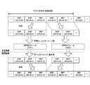
- FIG. 2 is a diagram for describing stream division in the first embodiment of the present technology.
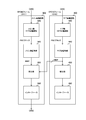
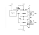
- FIG. 1 is a block diagram illustrating a configuration example of a main integrated circuit and a sub integrated circuit according to a first embodiment of the present technology.
- FIG. 2 is a block diagram illustrating a configuration example of a main integrated circuit and a sub integrated circuit in which a configuration on a sub side according to the first embodiment of the present technology is the same as that on the main side.
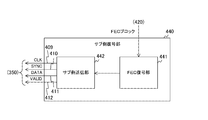
- FIG. 7 is a block diagram illustrating a configuration example of a sub-side decoding unit according to the first embodiment of the present technology.
- 3 is an example of a timing chart illustrating data transfer control according to the first embodiment of the present technology.
- 5 is a flowchart illustrating an example of a reception process of the reception device according to the first embodiment of the present technology.
- FIG. 5 is a flowchart illustrating an example of a combining process of the receiving device according to the first embodiment of the present technology.
- FIG. 21 is a block diagram illustrating a configuration example of a sub-side decoding unit according to a modification of the first embodiment of the present technology.
- 13 is an example of a timing chart illustrating data transfer control in a modification of the first embodiment of the present technology.
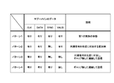
- FIG. 6 is a diagram illustrating an example of a data transfer pattern according to the first embodiment of the present technology and a modification example thereof.
- FIG. 11 is a block diagram illustrating a configuration example of a transmission device according to a second embodiment of the present technology.
- FIG. 11 is a diagram for describing a cell exchange procedure according to the second embodiment of the present technology.
- FIG. 21 is a block diagram illustrating a configuration example of a sub-side decoding unit according to a modification of the first embodiment of the present technology.
- 13 is an example of a timing chart illustrating data transfer control in a modification
- FIG. 14 is a block diagram illustrating a configuration example of a main integrated circuit and a sub integrated circuit according to a second embodiment of the present technology.
- FIG. 13 is a block diagram illustrating a configuration example of a main-side cell switching unit according to a second embodiment of the present technology. 13 is an example of a timing chart illustrating data transfer control according to the second embodiment of the present technology.
- Fig. 3 is a diagram illustrating an example of a data transfer pattern according to the embodiment of the present technology.
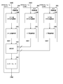
- FIG. 14 is a block diagram illustrating a configuration example of a main integrated circuit and a sub integrated circuit according to a third embodiment of the present technology.
- First Embodiment an example in which a receiving device performs channel bonding
- Second embodiment an example in which a receiver exchanges cells and performs channel bonding
- Third embodiment an example in which a receiving apparatus performs channel bonding between three or more frequency channels
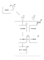
- FIG. 1 is a block diagram illustrating a configuration example of a communication system according to the first embodiment of the present technology.
- This communication system is a system for transmitting and receiving digital terrestrial broadcasting according to the ATSC 3.0 standard, and includes a transmitting device 100 and a receiving device 200.
- Transmission device 100 includes antenna 180. This transmitting apparatus 100 transmits data in OFDM frame units via a plurality of frequency channels.
- the antenna 180 transmits an RF signal that has been subjected to OFDM modulation.
- Receiving apparatus 200 includes antennas 210 and 215, RF receiving circuits 220 and 225, main integrated circuit 300 and sub integrated circuit 400, and decoded data processing unit 250.
- the antennas 210 and 215 receive RF signals through different frequency channels.
- the antenna 210 supplies the RF signal to the RF receiving circuit 220, and the antenna 215 supplies the RF signal to the RF receiving circuit 225.
- the RF reception circuits 220 and 225 perform AD (Analog to Digital) conversion and frequency conversion on an analog RF signal to obtain a baseband signal. Thereby, a baseband signal is received.
- the RF receiving circuit 220 supplies the baseband signal to the main integrated circuit 300 in OFDM frame units.
- the RF receiving circuit 225 supplies the baseband signal to the sub integrated circuit 400 in OFDM frame units. Note that the RF receiving circuit 220 is an example of a second receiving circuit described in the claims.
- the RF receiving circuit 225 is an example of a first receiving circuit described in the claims.
- the sub-integrated circuit 400 acquires a baseband packet (BBP: BaseBand Packets) by decoding an OFDM frame and outputs the acquired baseband packet to the main integrated circuit 300.
- BBP BaseBand Packets
- the sub integrated circuit 400 is an example of a first integrated circuit described in the claims.
- the main integrated circuit 300 acquires the BBP by decoding the OFDM frame and combines the BBP with the BBP from the sub integrated circuit 400.
- the main integrated circuit 300 supplies the combined data as decoded data to the decoded data processing unit 250. Note that the main integrated circuit 300 is an example of a second integrated circuit described in the claims.
- the decoded data processing unit 250 generates a video and an audio by performing a decoding process or the like on the decoded data, and outputs the generated video and audio to a display device and a speaker.
- FIG. 2 is a block diagram illustrating a configuration example of the transmission device 100 according to the first embodiment of the present technology.
- the transmission device 100 includes an input formatting block 110, a stream division block 120, and BICM (Bit Interleaved and Coded Modulation) blocks 130 and 135. Further, transmitting apparatus 100 includes framing / interleaving blocks 150 and 155, waveform generating sections 160 and 165, and RF transmitting circuit 170.
- BICM Bit Interleaved and Coded Modulation
- the input formatting block 110 encapsulates and compresses each of a plurality of input data to generate a BBP.
- the input formatting block 110 receives a plurality of pieces of data obtained by dividing a stream such as a video stream into fixed units.
- PLP Physical Layer Layer Pipe
- the input formatting block 110 encapsulates and compresses each of the data to generate an ALP (ATSC Link layer Protocol) packet. Then, the input formatting block 110 divides an ALP group including ALP packets corresponding to the PLP into a plurality of ALP groups for each PLP, and generates a BBP in which the divided data is stored in a payload. The input formatting block 110 supplies a stream including those BBPs to the stream segmentation block 120.
- ALP ATSC Link layer Protocol
- the stream division block 120 divides a stream according to the number of frequency channels used for channel bonding. Here, it is assumed that the stream is transmitted via two frequency channels.
- the stream division block 120 divides the stream into two in BBP units, supplies one of the divided data to the BICM block 130, and supplies the other to the BICM block 135.
- the BICM blocks 130 and 135 encode, for each PLP, a plurality of BBPs corresponding to the PLP, perform bit interleaving, and output a plurality of cells.
- the BICM block 130 outputs a cell group corresponding to PLP to the framing / interleaving block 150
- the BICM block 135 outputs a cell group corresponding to PLP to the framing / interleaving block 155.
- the framing and interleaving blocks 150 and 155 perform time interleaving and frequency interleaving on a group of cells corresponding to the PLP, and generate a group of symbols constituting an OFDM frame.
- the framing / interleaving block 150 outputs each of the symbol groups corresponding to the OFDM frame to the waveform generation unit 160.
- the framing / interleaving block 155 outputs each symbol group corresponding to the OFDM frame to the waveform generation unit 165.
- the waveform generation units 160 and 165 generate an OFDM frame by performing insertion of a pilot signal, inverse fast Fourier transform (IFFT), insertion of a guard interval, and the like. Waveform generation sections 160 and 165 output the OFDM frame to RF transmission circuit 170.
- IFFT inverse fast Fourier transform
- the RF transmission circuit 170 transmits the OFDM frame from the waveform generation unit 160 and the OFDM frame from the waveform generation unit 165 via different frequency channels.
- the RF transmission circuit 170 transmits the OFDM frame from the waveform generation unit 160 via, for example, the antenna 180 via the frequency channel CH1. Further, the RF transmission circuit 170 transmits the OFDM frame from the waveform generation unit 165, for example, from the antenna 180 via the frequency channel CH2. Note that, as described later, two RF receiving circuits and two antennas can be arranged.
- the transmitting apparatus 100 transmits an OFDM frame via two frequency channels when using channel bonding, the transmitting apparatus 100 can transmit an OFDM frame via three or more frequency channels.
- the processing in the transmitting device 100 is “ATSC Standard: Physical Layer Protocol Protocol Doc. A / 322: 2017”, Advanced Television Systems Comittee, the Internet (https://www.atsc.org/standards/atsc-3- 0-standards /) ".
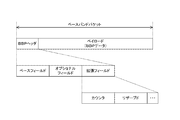
- FIG. 3 is a diagram illustrating an example of a data structure of a baseband packet (BBP) according to the first embodiment of the present technology.
- This BBP includes a BBP header and a payload.
- the BBP header includes a base field, an optional field, and an extension field.
- a counter and a reserved area are provided in the extension field. This counter linearly increases by one for each BBP in the PLP, and an independent counter is used for each PLP.
- the counter in the extension field is hereinafter referred to as “extension counter”.
- the data stored in the payload is referred to as “BBP data”.
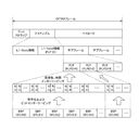
- FIG. 4 is a diagram illustrating an example of a data structure of an OFDM frame according to the first embodiment of the present technology.
- An OFDM frame includes a bootstrap, a preamble, and a payload.
- the preamble stores L1 information including L1-Basic information and L1-Detail information.
- the L1-Basic information stores a pilot signal encoding method and the like. Details of the L1-Detail information will be described later.
- the payload stores a maximum of 256 subframes. In addition, a maximum of 64 PLPs are stored in each subframe.
- the BICM block 130 and the like perform coding and bit interleaving on a BBP group corresponding to the PLP to generate a cell group corresponding to the PLP. Then, the framing / interleaving block 150 and the like generate a preamble while performing frequency interleaving and time interleaving on a cell group corresponding to PLP, and generate a symbol group constituting OFDM.
- FIG. 5 is a diagram illustrating an example of a syntax of L1-Detail information according to the first embodiment of the present technology. This syntax is described in "ATSC Standard: Physical Layer Protocol Doc. A / 322: 2017", Advanced Television Systems Committee, Internet (https://www.atsc.org / standards / atsc-3-0-standards /) ".
- a “L1D_plp_id” field is provided in a portion 601 surrounded by a broken line in the L1-Detail information.
- PLP identification information is described in the “L1D_plp_id” field.
- the part 602 is provided with an “L1D_plp_start” field that describes the index of the first cell in the current PLP in the current subframe.
- the part 603 is provided with an "L1D_plp_fec_type” field that describes an encoding method in forward error correction (FEC: Forward @ Error @ Correction).
- the part 604 is provided with an “L1D_plp_mod” field and an “L1D_plp_cod” field.
- the “L1D_plp_mod” field describes the modulation method used in the current PLP.
- the “L1D_plp_cod” field the current PLP coding rate is described.
- the portion 605 is provided with an “L1D_plp_num_channel_bonded” field that describes the number of frequencies included in the current PLP channel bonding.
- the value of this field is a value excluding the current channel frequency. For example, when using two frequencies, “1” is set in the “L1D_plp_num_channel_bonded” field.
- the receiving device 200 can determine whether or not to perform channel bonding by referring to the “L1D_plp_num_channel_bonded” field.
- the portion 606 is provided with an “L1D_plp_channel_bonding_format” field that describes the current PLP channel bonding format.
- FIG. 6 is a diagram for describing stream division in the first embodiment of the present technology.
- a BBP group corresponding to a certain PLP is divided into two in a stream.
- the value of the extension counter is assigned for each BBP, and the value is stored in the header.
- the extension counter is initialized with the first BBP in the PLP, and increments by one for each BBP.
- the stream division block 120 divides the BBP group corresponding to the PLP into, for example, a BBP group whose counter value is up to “12” and a BBP group whose counter value is “13” or later.
- the BICM block 130, the framing / interleaving block 150, and the waveform generating unit 160 perform encoding, interleaving, and the like on the former BBP group to generate an OFDM frame corresponding to the frequency channel CH1.
- the BICM block 135, the framing / interleaving block 155, and the waveform generating unit 165 perform encoding, interleaving, and the like on the latter BBP group to generate an OFDM frame corresponding to the frequency channel CH2.
- the receiving device 200 receives the above-described OFDM frame via the frequency channels CH1 and CH2, and performs a process corresponding to the transmitting side to set a BBP group whose counter value is up to “12” and a BBP group whose counter value is “13” and thereafter. And a BBP group. Then, receiving apparatus 200 restores the original stream by arranging (in other words, combining) those BBPs in the order of the counter values. Thus, receiving apparatus 200 can combine the BBP corresponding to frequency channel CH1 and the BBP corresponding to frequency channel CH2 by referring to the value of the extension counter in the BBP.
- FIG. 7 is a block diagram illustrating a configuration example of the main integrated circuit 300 and the sub integrated circuit 400 according to the first embodiment of the present technology.
- the main integrated circuit 300 includes a main-side OFDM demodulation unit 320, a main-side decoding unit 340, a combining unit 350, and an interface 360.
- the sub integrated circuit 400 includes a sub side OFDM demodulation section 420 and a sub side decoding section 440.
- the sub-side OFDM demodulation section 420 demodulates the OFDM frame from the RF receiving circuit 225 to obtain L1 information and a FEC block group corresponding to PLP, and supplies the obtained information to the sub-side decoding section 440.
- processing corresponding to the framing / interleaving block 155 and the waveform generation section 165 in the transmission device 100 is performed, and a cell group corresponding to PLP is generated.
- a deinterleave corresponding to the interleave in the BICM block 135 generates an FEC block group corresponding to the PLP.
- the sub-side OFDM demodulation section 420 is an example of a first demodulation section described in the claims.
- the sub-side decoding unit 440 decodes each FEC block corresponding to the PLP to obtain a BBP, and outputs the BBP to the combining unit 350.
- the sub-side decoding section 440 performs a decoding process corresponding to the encoding in the BICM block 135 in the transmitting device 100. Note that the sub-side decoding unit 440 is an example of a first decoding unit described in the claims.
- the main-side OFDM demodulation unit 320 demodulates the OFDM frame from the RF reception circuit 220 to obtain L1 information and a FEC block group corresponding to PLP, and supplies the obtained information to the main-side decoding unit 340.
- the main-side OFDM demodulation unit 320 is an example of a second demodulation unit described in the claims.
- the main-side decoding unit 340 decodes each FEC block corresponding to the PLP to obtain a BBP, and outputs the BBP to the combining unit 350. Note that the main-side decoding unit 340 is an example of a second decoding unit described in the claims.
- the combining unit 350 combines the BBP group from the main-side decoding unit 340 and the BBP group from the sub-side decoding unit 440 to restore the original stream.
- the combining unit 350 supplies the combined decoded data to the decoded data processing unit 250 via the interface 360.
- channel bonding is not essential, and is selectively used as needed. For example, whether to use channel bonding differs for each region. For this reason, a user in an area in which channel bonding is not expected to be used is provided with the receiving device 200 from which the sub integrated circuit 400 is deleted.
- the cost of the receiving device 200 can be significantly reduced.
- the circuit groups provided in the main integrated circuit 300 and the sub-integrated circuit 400 can be mounted on one integrated circuit, however, in this configuration, the cost is higher than in the configuration in which only the sub-integrated circuit 400 is deleted. turn into.
- both an integrated circuit using channel bonding and an integrated circuit not using channel bonding can be individually designed, but this increases the burden on the designer, which is not preferable.
- By providing circuits necessary for channel bonding separately in the main integrated circuit 300 and the sub integrated circuit 400 it is possible to easily provide both the receiving device 200 using channel bonding and the receiving device not using channel bonding. Can be.
- the sub-integrated circuit 400 is not provided with a coupling portion and an interface, but these circuits may be provided as illustrated in FIG.
- channel bonding is not always used during broadcasting. For example, channel bonding is used only when high-definition content is transmitted.
- the receiving apparatus 200 determines whether to perform channel bonding by referring to “L1D_plp_num_channel_bonded”. Then, when the channel bonding is not performed, the receiving device 200 sets the sub-integrated circuit 400 to disable and stops. Thus, power consumption can be reduced.
- each of the main integrated circuit 300 and the sub-integrated circuit 400 can detect the presence or absence of a failure by self-diagnosis. Then, when a failure occurs in one, the integrated circuit is disabled in the other. In the configuration shown in the figure, a stream can be output only with the sub-side integrated circuit 400 alone. Thereby, the reliability of the receiving device 200 can be improved.
- FIG. 9 is a block diagram illustrating a configuration example of the sub-side decoding unit 440 according to the first embodiment of the present technology.
- the sub-side decoding section 440 includes an FEC decoding section 441 and a sub-side transmitting section 442.
- the FEC decoding unit 441 decodes each FEC block to generate a BBP.
- the FEC decoding unit 441 supplies a BBP group corresponding to the PLP to the sub-side transmitting unit 442.
- the sub-side transmission unit 442 adds header information to the BBP group and transmits the BBP group to the combining unit 350.
- the sub-side transmission unit 442 is connected to the coupling unit 350 via a clock line 409, a sync line 410, a data line 411, and a valid line 412.
- the clock line 409 is a signal line for transmitting the clock signal CLK.
- the sync line 410 is a signal line for transmitting the synchronization signal SYNC.
- the data line 411 is a signal line for transmitting a data signal DATA such as header information and BBP data.
- the physical number of the data lines 411 is plural in parallel transfer, but is one in serial transfer. Hereinafter, even in the case of parallel transfer, the data line 411 is treated as one for convenience of description.
- the valid line 412 is a signal line for transmitting a data valid signal VALID indicating whether or not the data being transmitted is valid.
- FIG. 10 is an example of a timing chart illustrating data transfer control according to the first embodiment of the present technology.
- the sub-side transmission unit 442 generates a clock signal CLK having a predetermined frequency and transmits the clock signal CLK to the sub-side.
- the sub-side transmission unit 442 transmits a synchronization signal SYNC for synchronizing with the reception side. Further, the sub-side transmitting section 442 transmits the header information during a period from timing T0 to T1, and transmits the BBP data in synchronization with the clock signal CLK from timing T1 to timing T2. After the timing T3, the next header information and BBP data are transmitted.
- the timing T2 to T3 is a gap period during which valid data is not transmitted. In this period, the data valid signal VALID is set to the low level, and in other periods, it is set to the high level.
- the header information includes, for example, PLP identification information, an encoding method and an encoding rate, a BBP error flag, and a sub-side decoding lock flag.
- PLP @ ID indicates PLP identification information
- FEC @ TYPE indicates an encoding method
- FEC COD indicates the coding rate.
- L1D_plp_id The value of the “L1D_plp_id” field in the L1 information is set in “PLP @ ID”. This identification information is used when using M-PLP.
- the value of the “L1D_plp_fec_type” field in the L1 information is set in “FEC @ TYPE”.
- FEC @ COD the value of the “L1D_plp_cod” field in the L1 information is set.
- the BBP error flag indicates whether or not the sub-side decoding unit 440 has detected an error when decoding the FEC block and acquiring the BBP.
- the sub-side decoding lock flag indicates whether or not the number of times that the sub-side decoding unit 440 has determined that there is no error continuously when decoding is equal to or more than a certain number of times. For example, the sub-side decoding lock flag is set to ON when the number of consecutive determinations that there is no error is equal to or more than a certain number. These flags are generated by the sub-side decoding unit 440 and are used when combining.
- the coupling unit 350 on the receiving side detects the head of the header information based on the synchronization signal SYNC, and receives data in synchronization with the clock signal CLK within a period in which the data valid signal VALID is at a high level.
- the header information and the BBP data are also transmitted from the main decoding unit 340 to the combining unit 350 in the same manner as the sub decoding unit 440.
- the header information from the main decoding unit 340 includes a main decoding lock flag instead of the sub decoding lock flag.
- FIG. 11 is a flowchart illustrating an example of a reception process of the reception device 200 according to the first embodiment of the present technology.
- the reception process is started, for example, when a predetermined application for the reception device 200 to receive broadcast data is executed.
- the RF receiving circuits 220 and 225 in the receiving device 200 receive the OFDM frame via different frequency channels (step S901).
- the sub integrated circuit 400 and the main integrated circuit 300 demodulate and decode the corresponding OFDM frame to obtain a BBP (step S902).
- the main integrated circuit 300 executes a combining process for combining the BBPs (Step S910).
- receiving apparatus 200 ends the receiving process.
- FIG. 12 is a flowchart illustrating an example of the combining process of the receiving device 200 according to the first embodiment of the present technology.
- the combining unit 350 determines whether both the main-side decryption lock flag and the sub-side decryption lock flag are on (step S911). When at least one of the main-side decryption lock flag and the sub-side decryption lock flag is off (step S911: No), the combining unit 350 repeats step S911 and the subsequent steps.
- step S911 When both the main-side decryption lock flag and the sub-side decryption lock flag are on (step S911: Yes), the combining unit 350 acquires the BBPs on the main side and the sub side (step S912).
- Step S913 If the certain condition is not satisfied (Step S913: No), the combining unit 350 repeats Step S912 and subsequent steps. On the other hand, when a certain condition is satisfied (step S913: Yes), the combining unit 350 combines the BBPs using the extension counter and restores the original stream (step S914). After step S914, the combining unit 350 ends the combining process.
- the sub integrated circuit 400 outputs the BBP of the channel CH2, and the main integrated circuit 300 acquires the BBP of the channel CH1 and couples it with the BBP of the channel CH1.
- channel bonding according to the ATSC 3.0 standard can be realized.
- the sub-integrated circuit 400 transmits data via the four signal lines of the clock line 409, the sink line 410, the data line 411, and the valid line 412. From the viewpoint of reduction, it is desirable that the number of signal lines is small.
- the sub-integrated circuit 400 according to the modification of the first embodiment differs from the first embodiment in that data is transmitted via three or less signal lines.
- FIG. 13 is a block diagram illustrating a configuration example of the sub-side decoding unit 440 according to a modified example of the first embodiment of the present technology.
- the sub-side decoding unit 440 according to the modification of the first embodiment is different from the first-side decoding unit 440 in that the sub-side decoding unit 440 is connected to the main-side coupling unit 350 via the clock line 409, the data line 411, and the valid line 412. Different from the embodiment.
- FIG. 14 is an example of a timing chart showing data transfer control according to a modification of the first embodiment of the present technology.
- the sub-side decoding unit 440 transmits a synchronization signal of a predetermined data series via the data line 411 during a period from timing T0 to timing T1. Subsequently, the sub-side decoding unit 440 transmits the header information and the BBP data during the period from the timing T1 to the timing T2.
- the sub-side decoding unit 440 transmits the data valid signal VALID, but may not transmit the data valid signal VALID. This eliminates the need to wire the valid line 412, and data can be transmitted only by the clock line 409 and the data line 411. In this case, the sub-side decoding section 440 may continuously transmit data without providing a gap period.
- FIG. 15 is a diagram illustrating an example of a data transfer pattern according to the first embodiment of the present technology and a modification example thereof.
- a clock signal CLK a data signal DATA (such as header information and BBP data), a synchronization signal SYNC, and a data valid signal VALID are transmitted from the sub side to the main side via four signal lines.
- the clock signal CLK, the data signal DATA, and the data valid signal VALID are transmitted from the sub side to the main side via three signal lines.
- the configuration may be such that the clock signal CLK and the data signal DATA are transmitted from the sub side to the main side via two signal lines. Further, the configuration may be such that the clock signal CLK, the data signal DATA and the synchronization signal SYNC are transmitted from the sub side to the main side via three signal lines.
- the sub-side decoding section 440 may continuously transmit data without providing a gap period.
- the sub-side decoding unit 440 transmits the synchronization signal via the data line 411, and thus the sync line 410 for transmitting the synchronization signal. Can be omitted.
- the receiving apparatus 200 receives data via a plurality of frequency channels.
- the SNR Signal-Noise Ratio
- the receiving apparatus 200 according to the second embodiment is different from the first embodiment in that the SNR is improved by performing cell switching.
- FIG. 16 is a block diagram illustrating a configuration example of the transmission device 100 according to the second embodiment of the present technology.
- This transmitting apparatus 100 is different from the first embodiment in further including a cell switching block 140, an RF transmitting circuit 175, and an antenna 185.
- the cell exchange block 140 exchanges cells between different frequency channels. This cell switching block 140 is inserted between BICM blocks 130 and 135 and framing and interleaving blocks 150 and 155. The cell exchange block 140 exchanges an odd-numbered cell of the frequency channel CH1 and an odd-numbered cell of the frequency channel CH2 in a cell group corresponding to PLP. On the other hand, the even-numbered cells of the frequency channel CH1 and the even-numbered cells of the frequency channel CH2 are not exchanged. The cell switching block 140 outputs the even-numbered cells that have not been replaced or the odd-numbered replaced cells to the framing / interleaving blocks 150 and 155. Further, RF transmitting circuit 170 transmits the OFDM frame from waveform generating section 160 from antenna 180, and RF transmitting circuit 175 transmits the OFDM frame from waveform generating section 165 from antenna 185.
- cell exchange is not essential and is performed as needed. Whether the cell exchange has been performed on the transmission side can be grasped by the reception side by referring to “L1D_plp_channel_bonding_format” in the L1 information.
- FIG. 17 is a diagram for describing a cell exchange procedure in the second embodiment of the present technology.
- "A” in the figure shows the processing of the cell exchange block 140 for the first cell.
- “B” in the figure shows the processing of the cell exchange block 140 for the second cell.
- c indicates the processing of the cell exchange block 140 for the third cell.
- the i-th input cell in the cell group corresponding to the PLP of the frequency channel CH1 is denoted by si , 1 .
- i is (are N CELL integer) N CELL the number of cells constituting the PLP When an input integer index of 1 to N CELL.
- the i-th input cell of the cell group corresponding to the PLP of the frequency channel CH2 is assumed to be si, 2 .
- the i-th output cell in the cell group corresponding to the PLP of the frequency channel CH1 is defined as gi , 1 .
- the i-th output cell in the cell group corresponding to the PLP of the frequency channel CH2 is defined as gi , 2 . If i is odd, the relationship between the input and output cells is given by:
- the 0-th input cell s 0, 1 of the frequency channel CH1 is output as the 0-th output cell g 0, 1 of the frequency channel CH1.
- 0-th input cell s 0, 2 frequency channel CH2 is output as the 0-th output cell g 0, 2 frequency channel CH2.
- the first input cell s 1,1 of the frequency channel CH1 is output as the first output cell g 1,2 of the frequency channel CH2, as exemplified by b in FIG.
- the first input cell s 1,2 of the frequency channel CH2 is output as the first output cell g 1,1 of the frequency channel CH1.
- the second input cell s 2,1 of the frequency channel CH1 is output as the second output cell g 2,1 of the frequency channel CH1.
- the second input cell s 2,2 of the frequency channel CH2 is output as the second output cell g 2,2 of the frequency channel CH2.
- odd-numbered cells are exchanged, and even-numbered cells are output without being exchanged.
- FIG. 18 is a block diagram illustrating a configuration example of a main integrated circuit 300 and a sub integrated circuit 400 according to the second embodiment of the present technology.
- the main integrated circuit 300 according to the second embodiment differs from the first embodiment in that a main-side cell switching unit 330 is further provided.
- the sub-integrated circuit 400 according to the second embodiment is different from the first embodiment in that the sub-integrated circuit 400 further includes a sub-side cell switching unit 430.
- the main-side cell exchange section 330 acquires an input index of a cell and exchanges a cell with the sub-side when the input index is an odd number. On the other hand, if the index is even, no cells are exchanged.
- the main-side cell switching unit 330 supplies the exchanged cells or the non-exchanged cells to the main-side decoding unit 340 in units of FEC blocks.
- the main-side cell switching unit 330 is an example of a second cell switching unit described in the claims.
- the sub-side cell exchange section 430 acquires an input index of a cell and exchanges a cell with the main side when the input index is an odd number. On the other hand, if the input index is even, no cells are exchanged.
- the sub-side cell switching unit 430 supplies the exchanged cell or the cell that has not been exchanged to the sub-side decoding unit 440 in units of FEC blocks. Note that the sub-side cell switching unit 430 is an example of a first cell switching unit described in the claims.
- the main-side OFDM demodulator 320 generates a main-side demodulation lock flag. For example, if the number of successful demodulations exceeds a certain number, the main demodulation lock flag is set to ON. Similarly, sub-side OFDM demodulation section 420 generates a sub-side demodulation lock flag.
- FIG. 19 is a block diagram illustrating a configuration example of the main-side cell switching unit 330 according to the second embodiment of the present technology.
- the main-side cell switching section 330 includes an FEC block counter 331, a cell transmission section 332, and a cell reception section 333.
- the FEC block counter 331 counts the number of FEC block inputs from the main-side OFDM demodulation unit 320.
- the FEC block counter 331 refers to “L1D_plp_start” in the L1 information, initializes the count value when the first FEC block in the PLP is input, and counts the count value each time the FEC block is input. .
- the FEC block counter 331 supplies the count value of the FEC block counter as the FEC block counter value to the cell transmission unit 332 and the cell reception unit 333 together with the L1 information.
- the cell transmission unit 332 acquires the input index of the cell, and transmits the cell to the sub-side cell switching unit 430 when the input index is an odd number.
- the cell transmitting unit 332 is connected to the sub-cell switching unit 430 via the clock line 401, the sync line 402, the data line 403, and the valid line 404, and transmits cells via these signal lines.
- the cell transmission unit 332 acquires the coding method and coding rate of the FEC block from the L1 information on the main side. Then, the cell transmitting unit 332 transmits the main-side encoding method, the encoding rate, and the main-side demodulation lock flag to the sub-side together with the FEC block counter value. In addition, the cell transmission unit 332 receives, from the cell reception unit 333, the sub-side encoding method, the encoding rate, the sub-side demodulation lock flag, and the FEC block counter value.
- the cell transmission unit 332 and the cell reception unit 333 start cell exchange when the main demodulation lock flag and the sub demodulation lock flag are on.
- the cell transmission unit 332 determines whether or not the encoding method, the encoding rate, and the FEC block counter value on the main side match the sub-side, and when they match, the size of the FEC block is determined based on the information. Calculate in cell units.
- the cell transmitting unit 332 divides the FEC block into cells, transmits odd-numbered (input index) cells to the sub side, and transmits even-numbered (input index) cells to the cell receiving unit 333. Supply.
- the cell receiving unit 333 receives the coding method, the coding rate, the sub-side demodulation lock flag, the FEC block counter value, and the cell from the sub-side cell switching unit 430.
- the cell receiving unit 333 is connected to the sub-side cell switching unit 430 via the clock line 405, the sink line 406, the data line 407, and the valid line 408, and receives cells and the like via these signal lines.
- the cell receiving unit 333 supplies the received coding scheme, coding rate, sub-side demodulation lock flag, and FEC block counter value to the cell transmitting unit 332. Then, the cell receiving unit 333 generates an FEC block from the even-numbered cells from the cell transmitting unit 332 and the received odd-numbered cells, and supplies the FEC block to the main-side decoding unit 340.
- the configuration of the sub-cell switching section 430 is the same as that of the main-cell switching section 330.
- FIG. 20 is an example of a timing chart showing data transfer control according to the second embodiment of the present technology.
- the main-side cell switching unit 330 transmits a synchronization signal SYNC for synchronizing with the reception side.
- the main-side cell switching unit 330 transmits the header information during a period from timing T0 to T1, and transmits cells in synchronization with the clock signal CLK from timing T1 to timing T2.
- the next header information and cell are transmitted.
- the timing T2 to T3 is a gap period during which no valid data is transmitted. In this period, the data valid signal VALID is set to the low level, and in other periods, it is set to the high level.
- the header information includes, for example, PLP identification information, an encoding method and an encoding rate, an FEC block counter value, and a main-side demodulation lock flag.
- the header information transmitted from the sub side includes a sub side demodulation lock flag in addition to the PLP identification information.
- FIG. 21 is a diagram illustrating an example of a data transfer pattern according to the embodiment of the present technology.
- a clock signal CLK, a synchronization signal SYNC, a data signal DATA and a data valid signal are bidirectionally transmitted between the sub side and the main side via four signal lines.
- the signal VALID is transmitted.
- the clock signal CLK, the data signal DATA, and the data valid signal VALID can be transmitted bidirectionally between the sub side and the main side via three signal lines.
- the synchronization signal is transmitted via the data line.
- the clock signal CLK and the data signal DATA can be transmitted bidirectionally between the sub side and the main side via two signal lines. In this case, data is continuously transmitted without a gap period.
- a clock signal CLK, a data signal DATA, and a synchronization signal SYNC can be transmitted bidirectionally between the sub side and the main side via three signal lines. In this case, data is continuously transmitted without a gap period.
- the clock signal line on the main side can be shared by the sub side.
- the sub-side does not transmit the clock signal CLK as illustrated in patterns 5 to 8.
- Other configurations are the same as the patterns 1 to 4.
- the clock signal line on the sub side can be shared by the main side.
- the main side does not transmit the clock signal CLK.
- Other configurations are the same as the patterns 1 to 4.
- the receiving device 200 since the receiving device 200 exchanges the odd-numbered cells between different frequency channels, the SNR is improved as compared with the case where the cells are not exchanged. be able to.
- FIG. 22 is a block diagram illustrating a configuration example of a main integrated circuit and a sub integrated circuit according to the third embodiment of the present technology.
- the receiving device 200 according to the third embodiment is different from the first embodiment in further including a sub-integrated circuit 500.
- the sub integrated circuit 500 demodulates and decodes the OFDM frame received via the frequency channel RF3 different from the frequency channels CH1 and CH2.
- the sub integrated circuit 500 includes a sub side OFDM demodulation section 520 and a sub side decoding section 540.
- the configurations of the sub-side OFDM demodulation section 520 and the sub-side decoding section 540 are the same as the sub-side OFDM demodulation section 420 and the sub-side decoding section 440.
- the sub-integrated circuit 500 acquires the BBP and supplies it to the coupling unit 350.
- the combining unit 350 combines the BBPs from the main-side decoding unit 340 and the sub-integrated circuits 400 and 500 to restore the stream.
- the receiving device 200 can receive data via four or more frequency channels by adding a sub-integrated circuit.
- the receiving device 200 receives data via three frequency channels, and thus has a higher frequency band than when receiving via two frequency channels. Can be wider.
- the processing procedure described in the above-described embodiment may be regarded as a method having these series of procedures, or a program for causing a computer to execute these series of procedures or a recording medium storing the program. May be caught.
- a recording medium for example, a CD (Compact Disc), an MD (MiniDisc), a DVD (Digital Versatile Disc), a memory card, a Blu-ray Disc (Blu-ray (registered trademark) Disc), or the like can be used.
- the present technology may have the following configurations. (1) a first receiving circuit for receiving, via a first frequency channel, a first frame in which the first packet in a stream including first and second packets is encoded; A second receiving circuit that receives a second frame in which the second packet is encoded via a second frequency channel different from the first frequency channel; A first integrated circuit that decodes the first frame to obtain the first packet; A reception device comprising: a second integrated circuit that performs a process of decoding the second frame to obtain the second packet and a process of combining the first and second packets to restore the stream. apparatus.
- the first integrated circuit includes: A first demodulation unit that demodulates the first frame to obtain a plurality of first input cells; A first cell exchange unit that exchanges a part of the plurality of first input cells with the second integrated circuit and outputs each of the replaced cells as a first output cell; A first decoding unit that decodes the first output cell to obtain the first packet,
- the second integrated circuit includes: A second demodulation unit that demodulates the second frame to obtain a plurality of second input cells; A second cell exchange unit that exchanges a part of the plurality of second input cells with the first integrated circuit and outputs each of the exchanged cells as a second output cell; A second decoding unit that decodes the second output cell to obtain the second packet;
- the receiving device further comprising: a combining unit configured to combine the first and second packets to restore the stream.
- the first cell exchange unit acquires a numerical value corresponding to the input index of the first input cell, and performs exchange of the first input cell when the input index is odd.
- the first switching cell transmits at least one of a clock signal, a numerical value corresponding to the input index, a synchronization signal, and a data valid signal to the second switching cell together with the first input cell.
- the second switching cell transmits at least one of a clock signal, a numerical value corresponding to the input index, a synchronization signal, and a data valid signal to the first switching cell together with the second input cell.
- the receiving device according to (3) or (4).
- the receiving device wherein the second integrated circuit combines the first and second packets when a predetermined condition is satisfied.
- the first frame includes a first encoded block obtained by encoding the first packet;
- the second frame includes a second encoded block obtained by encoding the second packet,
- the first integrated circuit determines the presence / absence of an error in the first packet each time the first encoded block is decoded, and the number of consecutive determinations that there is no error exceeds a predetermined number.
- a first decryption lock flag is generated
- the second integrated circuit determines the presence or absence of an error in the second packet each time the first encoded block is decoded, and when the number of times continuously determining that there is no error exceeds a predetermined number.
- the receiving device according to (6) further comprising: generating a second decryption lock flag; and starting combining the first and second packets when the first and second decryption lock flags are generated.
- the receiving device according to (8), wherein the second integrated circuit combines the first packet determined to have no error and the second packet determined to have no error. .
- the first integrated circuit transmits at least one of a clock signal, a synchronization signal, and a data valid signal together with the first packet to the second integrated circuit.
- the receiving device according to any one of the above.
- the receiving device according to any one of (1) to (9), wherein the first and second frames are frames compliant with ATSC (Advanced Television Systems Committee standards) 3.0 standard.
- a first frame in which the first packet in the stream including the first and second packets is encoded is transmitted via a first frequency channel, and the second frame in which the second packet is encoded is transmitted.
- a transmitting apparatus for transmitting the second frame through a second frequency channel different from the first frequency channel; A first receiving circuit for receiving the first frame via the first frequency channel; A second receiving circuit for receiving the second frame via the second frequency channel; A first integrated circuit that decodes the first frame to obtain the first packet; A communication including a second integrated circuit that performs a process of decoding the second frame to obtain the second packet and a process of combining the first and second packets to restore the stream. system.
- a second integrated circuit performs a process of decoding the second frame to obtain the second packet and a process of combining the first and second packets to restore the stream.
- a control method for the receiving device comprising:
Landscapes
- Engineering & Computer Science (AREA)
- Multimedia (AREA)
- Signal Processing (AREA)
- Two-Way Televisions, Distribution Of Moving Picture Or The Like (AREA)
- Time-Division Multiplex Systems (AREA)
- Circuits Of Receivers In General (AREA)
Abstract
ATSC3.0規格の地上波デジタル放送を受信する受信装置において、チャネルボンディングを実現する。 第1の受信回路は、第1および第2のパケットを含むストリーム内の第1のパケットが符号化された第1のフレームを第1の周波数チャネルを介して受信する。第2の受信回路は、第2のパケットが符号化された第2のフレームを第1の周波数チャネルと異なる第2の周波数チャネルを介して受信する。第1の集積回路は、第1のフレームを復号して前記第1のパケットを取得する。第2の集積回路は、第2のフレームを復号して第2のパケットを取得する処理と第1および第2のパケットを結合して前記ストリームを復元する処理とを行う。
Description
本技術は、受信装置、通信システム、および、受信装置の制御方法に関する。詳しくは、地上波デジタル放送を受信する受信装置、通信システム、および、受信装置の制御方法に関する。
近年、ATSC(Advanced Television Systems Committee standards)3.0規格を用いた次世代の地上波デジタル放送を受信するための受信装置の開発や研究が進められている。このATSC3.0規格では、周波数帯域の利用効率を向上させるために、チャネルボンディングと呼ばれる技術を用いることが予定されている(例えば、非特許文献1参照。)。ここで、チャネルボンディングとは、送信装置が1つのストリームを複数のデータに分割して互いに異なる周波数チャネルを介して送信した際に、それらのデータを受信装置が受信して結合することを意味する。
"ATSC Standard:Physical Layer Protocol Doc. A/322:2017"、Advanced Television Systems Committee、インターネット(https://www.atsc.org/standards/atsc-3-0-standards/)
上述の従来技術では、チャネルボンディングを用いて周波数帯域の利用効率を向上させることができる。しかしながら、非特許文献1には、送信側の仕様について記載されている一方で、受信側の仕様については記載されていない。このため、チャネルボンディングに対応した受信装置の開発が求められている。
本技術はこのような状況に鑑みて生み出されたものであり、ATSC3.0規格の地上波デジタル放送を受信する受信装置において、チャネルボンディングを実現することを目的とする。
本技術は、上述の問題点を解消するためになされたものであり、その第1の側面は、第1および第2のパケットを含むストリーム内の上記第1のパケットが符号化された第1のフレームを第1の周波数チャネルを介して受信する第1の受信回路と、上記第2のパケットが符号化された第2のフレームを上記第1の周波数チャネルと異なる第2の周波数チャネルを介して受信する第2の受信回路と、上記第1のフレームを復号して上記第1のパケットを取得する第1の集積回路と、上記第2のフレームを復号して上記第2のパケットを取得する処理と上記第1および第2のパケットを結合して上記ストリームを復元する処理とを行う第2の集積回路とを具備する受信装置、および、その制御方法である。これにより、第1および第2の周波数チャネルを介して取得された第1および第2のパケットからストリームが復元されるという作用をもたらす。
また、この第1の側面において、上記第1の集積回路は、上記第1のフレームを復調して複数の第1入力セルを取得する第1の復調部と、上記複数の第1入力セルの一部を上記第2の集積回路との間で交換して交換後のセルのそれぞれを第1出力セルとして出力する第1のセル交換部と、上記第1出力セルを復号して上記第1のパケットを取得する第1の復号部とを備え、上記第2の集積回路は、上記第2のフレームを復調して複数の第2入力セルを取得する第2の復調部と、上記複数の第2入力セルの一部を上記第1の集積回路との間で交換して交換後のセルのそれぞれを第2出力セルとして出力する第2のセル交換部と、上記第2出力セルを復号して上記第2のパケットを取得する第2の復号部と、上記第1および第2のパケットを結合して上記ストリームを復元する結合部とを備える。これにより、セルが交換されるという作用をもたらす。
また、この第1の側面において、上記第1のセル交換部は、上記第1入力セルの入力インデックスに応じた数値を取得し、当該入力インデックスが奇数である場合には上記第1入力セルの交換を行い、上記第2のセル交換部は、上記第2入力セルの入力インデックスを取得し、当該入力インデックスが奇数である場合には上記第2入力セルの交換を行ってもよい。これにより、奇数個目のセルのみが交換されるという作用をもたらす。
また、この第1の側面において、上記第1のセル交換部は、クロック信号、上記入力インデックスに応じた数値、同期信号およびデータ有効信号の少なくとも1つを上記第1入力セルとともに上記第2のセル交換部に送信してもよい。これにより、第1入力セルが確実に伝送されるという作用をもたらす。
また、この第1の側面において、上記第2の交換セルは、クロック信号、上記入力インデックスに応じた数値、同期信号およびデータ有効信号の少なくとも1つを上記第2入力セルとともに上記第1の交換セルに送信してもよい。これにより、第2入力セルが確実に伝送されるという作用をもたらす。
また、この第1の側面において、上記第2の集積回路は、所定の条件を満たす場合には上記第1および第2のパケットを結合してもよい。これにより、条件を満たすパケットのみが結合されるという作用をもたらす。
また、この第1の側面において、上記第1のフレームは、上記第1のパケットを符号化した第1符号化ブロックを含み、上記第2のフレームは、上記第2のパケットを符号化した第2符号化ブロックを含み、上記第1の集積回路は、上記第1の符号化ブロックの復号のたびに上記第1のパケットの誤りの有無を判断し、上記誤りが無いと連続して判断した回数が所定回数を超えた場合には第1の復号ロックフラグを生成し、上記第2の集積回路は、上記第1の符号化ブロックの復号のたびに上記第2のパケットの誤りの有無を判断し、上記誤りが無いと連続して判断した回数が所定回数を超える場合には第2の復号ロックフラグを生成し、上記第1および第2の復号ロックフラグが生成されたときに上記第1および第2のパケットの結合を開始してもよい。これにより、伝送状態が良好である場合にパケットが結合されるという作用をもたらす。
また、この第1の側面において、上記第2の集積回路は、上記誤りが無いと判断された上記第1のパケットと上記誤りが無いと判断された上記第2のパケットとを結合してもよい。これにより、誤りの無いパケット同士が結合されるという作用をもたらす。
また、この第1の側面において、上記第1の集積回路は、クロック信号、同期信号およびデータ有効信号の少なくとも1つを上記第1のパケットとともに上記第2の集積回路に送信してもよい。これにより、パケットが確実に伝送されるという作用をもたらす。
また、この第1の側面において、上記第1および第2のフレームは、ATSC(Advanced Television Systems Committee standards)3.0規格に準拠したフレームであってもよい。これにより、ATSC3.0規格の地上波デジタル放送が受信されるという作用をもたらす。
また、本技術の第2の側面は、第1および第2のパケットを含むストリーム内の上記第1のパケットを符号化した第1のフレームを第1の周波数チャネルを介して送信するとともに上記第2のパケットを符号化した第2のフレームを上記第1の周波数チャネルと異なる第2の周波数チャネルを介して送信する送信装置と、上記第1のフレームを上記第1の周波数チャネルを介して受信する第1の受信回路と、上記第2のフレームを上記第2の周波数チャネルを介して受信する第2の受信回路と、上記第1のフレームを復号して上記第1のパケットを取得する第1の集積回路と、上記第2のフレームを復号して上記第2のパケットを取得する処理と上記第1および第2のパケットを結合して上記ストリームを復元する処理とを行う第2の集積回路とを具備する通信システムである。これにより、第1および第2の周波数チャネルを介して送信された第1および第2のフレームから、第1および第2のパケットが取得され、それらのパケットからストリームが復元されるという作用をもたらす。
本技術によれば、ATSC3.0規格の地上波デジタル放送を受信する受信装置において、チャネルボンディングを実現することができるという優れた効果を奏し得る。なお、ここに記載された効果は必ずしも限定されるものではなく、本開示中に記載されたいずれかの効果であってもよい。
以下、本技術を実施するための形態(以下、実施の形態と称する)について説明する。説明は以下の順序により行う。
1.第1の実施の形態(受信装置がチャネルボンディングを行う例)
2.第2の実施の形態(受信装置がセルを交換し、チャネルボンディングを行う例)
3.第3の実施の形態(受信装置が3つ以上の周波数チャネル間でチャネルボンディングを行う例)
1.第1の実施の形態(受信装置がチャネルボンディングを行う例)
2.第2の実施の形態(受信装置がセルを交換し、チャネルボンディングを行う例)
3.第3の実施の形態(受信装置が3つ以上の周波数チャネル間でチャネルボンディングを行う例)
<1.第1の実施の形態>
[通信システムの構成例]
図1は、本技術の第1の実施の形態における通信システムの一構成例を示すブロック図である。この通信システムは、ATSC3.0規格の地上波デジタル放送を送受信するシステムであり、送信装置100および受信装置200を備える。
[通信システムの構成例]
図1は、本技術の第1の実施の形態における通信システムの一構成例を示すブロック図である。この通信システムは、ATSC3.0規格の地上波デジタル放送を送受信するシステムであり、送信装置100および受信装置200を備える。
送信装置100は、アンテナ180を備える。この送信装置100は、複数の周波数チャネルを介してデータをOFDMフレーム単位で送信する。アンテナ180は、OFDM変調を行ったRF信号を送信する。
受信装置200は、アンテナ210および215と、RF受信回路220および225と、メイン集積回路300およびサブ集積回路400と、復号データ処理部250とを備える。
アンテナ210および215は、互いに異なる周波数チャネルを介してRF信号を受信するものである。アンテナ210は、RF信号をRF受信回路220に供給し、アンテナ215は、RF信号をRF受信回路225に供給する。
RF受信回路220および225は、アナログのRF信号に対してAD(Analog to Digital)変換や周波数変換を行ってベースバンド信号を取得するものである。これにより、ベースバンド信号が受信される。RF受信回路220は、ベースバンド信号をOFDMフレーム単位でメイン集積回路300に供給する。RF受信回路225は、ベースバンド信号をOFDMフレーム単位でサブ集積回路400に供給する。なお、RF受信回路220は、特許請求の範囲に記載の第2の受信回路の一例である。RF受信回路225は、特許請求の範囲に記載の第1の受信回路の一例である。
サブ集積回路400は、OFDMフレームの復号によりベースバンドパケット(BBP:BaseBand Packets)を取得してメイン集積回路300に出力するものである。なお、サブ集積回路400は、特許請求の範囲に記載の第1の集積回路の一例である。
メイン集積回路300は、OFDMフレームの復号によりBBPを取得し、サブ集積回路400からのBBPと結合するものである。このメイン集積回路300は、結合後のデータを復号データとして復号データ処理部250に供給する。なお、メイン集積回路300は、特許請求の範囲に記載の第2の集積回路の一例である。
復号データ処理部250は、復号データに対してデコード処理などを行うことにより映像や音声を生成し、表示装置やスピーカーに出力するものである。
[送信装置の構成例]
図2は、本技術の第1の実施の形態における送信装置100の一構成例を示すブロック図である。この送信装置100は、入力フォーマッティングブロック110と、ストリーム分割ブロック120と、BICM(Bit Interleaved and Coded Modulation)ブロック130および135とを備える。また、送信装置100は、フレーム化・インターリービングブロック150および155と、波形生成部160および165と、RF送信回路170とを備える。
図2は、本技術の第1の実施の形態における送信装置100の一構成例を示すブロック図である。この送信装置100は、入力フォーマッティングブロック110と、ストリーム分割ブロック120と、BICM(Bit Interleaved and Coded Modulation)ブロック130および135とを備える。また、送信装置100は、フレーム化・インターリービングブロック150および155と、波形生成部160および165と、RF送信回路170とを備える。
入力フォーマッティングブロック110は、入力された複数のデータのそれぞれをカプセル化および圧縮してBBPを生成するものである。この入力フォーマッティングブロック110には、映像ストリームなどのストリームを一定の単位で分割した複数のデータが入力される。
ここで、ATSC3.0規格では、データは、PLP(Physical Layer Pipe)と呼ばれるデータ構造において伝送される。そして、送信側は、64PLPまで伝送することができ、受信側は最大4PLPまで同時処理することができなければならない。
入力フォーマッティングブロック110は、データのそれぞれをカプセル化および圧縮して、ALP(ATSC Link layer Protocol)パケットを生成する。そして、入力フォーマッティングブロック110は、PLPごとに、PLPに対応するALPパケットからなるALP群を複数に分割し、その分割したデータをペイロードに格納したBBPを生成する。入力フォーマッティングブロック110は、それらのBBPを含むストリームをストリーム分割ブロック120に供給する。
ストリーム分割ブロック120は、チャネルボンディングに用いる周波数チャネルの個数に応じてストリームを分割するものである。ここでは、2つの周波数チャネルを介してストリームを送信するものとする。ストリーム分割ブロック120は、ストリームをBBP単位で2つに分割し、分割したデータの一方をBICMブロック130に供給し、他方をBICMブロック135に供給する。
BICMブロック130および135は、PLPごとに、PLPに対応する複数のBBPのそれぞれを符号化し、ビットインタリーブを行って複数のセルを出力するものである。BICMブロック130は、フレーム化・インターリービングブロック150へ、PLPに対応するセル群を出力し、BICMブロック135は、フレーム化・インターリービングブロック155へ、PLPに対応するセル群を出力する。
フレーム化・インターリービングブロック150および155は、PLPに対応するセル群に対して時間インターリーブおよび周波数インターリーブを行い、OFDMフレームを構成するシンボル群を生成するものである。フレーム化・インターリービングブロック150は、OFDMフレームに対応するシンボル群のそれぞれを波形生成部160に出力する。一方、フレーム化・インターリービングブロック155は、OFDMフレームに対応するシンボル群のそれぞれを波形生成部165に出力する。
波形生成部160および165は、パイロット信号の挿入、逆高速フーリエ変換(IFFT:Inverse Fast Fourier Transform)や、ガードインターバルの挿入などを行ってOFDMフレームを生成するものである。波形生成部160および165は、OFDMフレームをRF送信回路170に出力する。
RF送信回路170は、波形生成部160からのOFDMフレームと、波形生成部165からのOFDMフレームとを、互いに異なる周波数チャネルを介して送信するものである。このRF送信回路170は、波形生成部160からのOFDMフレームを、周波数チャネルCH1を介して、例えば、アンテナ180から送信する。また、RF送信回路170は、波形生成部165からのOFDMフレームを、周波数チャネルCH2を介して、例えば、アンテナ180から送信する。なお、後述するように、RF受信回路およびアンテナを2つずつ配置することもできる。
なお、周波数チャネルCH1およびCH2の周波数帯域は、互いに隣接している必要は無い。また、送信装置100は、チャネルボンディングを用いる際に2つの周波数チャネルを介してOFDMフレームを送信しているが、3つ以上の周波数チャネルを介してOFDMフレームを送信することもできる。また、送信装置100内の処理は、「"ATSC Standard:Physical Layer Protocol Doc. A/322:2017"、Advanced Television Systems Committee、インターネット(https://www.atsc.org/standards/atsc-3-0-standards/)」に記載されている。
図3は、本技術の第1の実施の形態におけるベースバンドパケット(BBP)のデータ構造の一例を示す図である。このBBPは、BBPヘッダおよびペイロードを含む。BBPヘッダには、ベースフィールド、オプショナルフィールドおよび拡張フィールドが設けられる。そして、拡張フィールドには、カウンタやリザーブドの領域が設けられる。このカウンタは、PLP内のBBPごとに1ずつ線形に増加する値であり、PLPごとに独立のカウンタが用いられる。拡張フィールド内のカウンタを以下、「拡張カウンタ」と称する。また、ペイロードに格納されたデータを「BBPデータ」と称する。
図4は、本技術の第1の実施の形態におけるOFDMフレームのデータ構造の一例を示す図である。OFDMフレームは、ブートストラップ、プリアンブルおよびペイロードを含む。プリアンブルには、L1-Basic情報およびL1-Detail情報からなるL1情報が格納される。L1-Basic情報には、パイロット信号の符号化方法などが格納される。L1-Detail情報の詳細については後述する。ペイロードには、最大で256個のサブフレームが格納される。また、サブフレームのそれぞれには、最大で64個のPLPが格納される。
BICMブロック130等は、PLPに対応するBBP群に対して符号化およびビットインターリービングを行い、PLPに対応するセル群を生成する。そして、フレーム化・インターリービングブロック150等は、PLPに対応するセル群に対して周波数インターリービングや時間インターリービングを行う一方でプリアンブルを生成し、OFDMを構成するシンボル群を生成する。
図5は、本技術の第1の実施の形態におけるL1-Detail情報の構文の一例を示す図である。この構文は、「ATSC Standard:Physical Layer Protocol Doc. A/322:2017"、Advanced Television Systems Committee、インターネット(https://www.atsc.org
/standards/atsc-3-0-standards/)」に記載されている。
/standards/atsc-3-0-standards/)」に記載されている。
L1-Detail情報内の破線で囲った部分601に「L1D_plp_id」フィールドが設けられる。この「L1D_plp_id」フィールドには、PLPの識別情報が記載される。
また、部分602には、現在のサブフレーム内において、現在のPLP内の最初のセルのインデックスを記載した「L1D_plp_start」フィールドが設けられる。部分603には、前方誤り訂正(FEC:Forward Error Correction)における符号化方式を記載した「L1D_plp_fec_type」フィールドが設けられる。
部分604には、「L1D_plp_mod」フィールドおよび「L1D_plp_cod」フィールドが設けられる。「L1D_plp_mod」フィールドには、現在のPLPで用いた変調方式が記載される。「L1D_plp_cod」フィールドには、現在のPLPの符号化率が記載される。
部分605には、現在のPLPのチャネルボンディングに含まれる周波数の個数を記載した「L1D_plp_num_channel_bonded」フィールドが設けられる。ただし、このフィールドの値は、現在のチャネルの周波数を除いた値である。例えば、2つの周波数を用いる場合には、「L1D_plp_num_channel_bonded」フィールドに「1」が設定される。受信装置200は、「L1D_plp_num_channel_bonded」フィールドを参照することにより、チャネルボンディングを行うか否かを判断することができる。
部分606には、現在のPLPのチャネルボンディングフォーマットを記載した「L1D_plp_channel_bonding_format」フィールドが設けられる。
図6は、本技術の第1の実施の形態におけるストリームの分割を説明するための図である。ストリーム内において、あるPLPに対応するBBP群を2つに分割する場合を考える。このBBP群において、BBPごとに拡張カウンタの値が割り当てられ、そのヘッダ内に値が格納される。拡張カウンタは、PLP内の先頭のBBPで初期化され、BBPごとに1つずつ増分する。
ストリーム分割ブロック120は、PLPに対応するBBP群を、例えば、カウンタ値が「12」までのBBP群と、カウンタ値が「13」以降のBBP群とに分割する。BICMブロック130、フレーム化・インターリービングブロック150および波形生成部160は、前者のBBP群に対して符号化やインターリービングなどを行って周波数チャネルCH1に対応するOFDMフレームを生成する。一方、BICMブロック135、フレーム化・インターリービングブロック155および波形生成部165は、後者のBBP群に対して符号化やインターリービングなどを行って周波数チャネルCH2に対応するOFDMフレームを生成する。
受信装置200は、周波数チャネルCH1およびCH2を介して、上述のOFDMフレームを受信し、送信側と対応する処理により、カウンタ値が「12」までのBBP群と、カウンタ値が「13」以降のBBP群とを取得する。そして、受信装置200は、それらのBBPをカウンタ値の順に配列する(言い換えれば、結合する)ことにより、元のストリームを復元する。このように、受信装置200は、BBP内の拡張カウンタの値を参照することにより、周波数チャネルCH1に対応するBBPと、周波数チャネルCH2に対応するBBPとを結合することができる。
[集積回路の構成例]
図7は、本技術の第1の実施の形態におけるメイン集積回路300およびサブ集積回路400の一構成例を示すブロック図である。メイン集積回路300は、メイン側OFDM復調部320、メイン側復号部340、結合部350およびインターフェース360を備える。また、サブ集積回路400は、サブ側OFDM復調部420およびサブ側復号部440を備える。
図7は、本技術の第1の実施の形態におけるメイン集積回路300およびサブ集積回路400の一構成例を示すブロック図である。メイン集積回路300は、メイン側OFDM復調部320、メイン側復号部340、結合部350およびインターフェース360を備える。また、サブ集積回路400は、サブ側OFDM復調部420およびサブ側復号部440を備える。
サブ側OFDM復調部420は、RF受信回路225からのOFDMフレームを復調してL1情報と、PLPに対応するFECブロック群とを取得し、サブ側復号部440に供給するものである。このサブ側OFDM復調部420においては、送信装置100内のフレーム化・インターリービングブロック155および波形生成部165と対応する処理が行われて、PLPに対応するセル群が生成される。そして、BICMブロック135内のインターリーブに対応するデインターリーブにより、PLPに対応するFECブロック群が生成される。なお、サブ側OFDM復調部420は、特許請求の範囲に記載の第1の復調部の一例である。
サブ側復号部440は、PLPに対応するFECブロックのそれぞれを復号してBBPを取得し、結合部350に出力するものである。このサブ側復号部440においては、送信装置100内のBICMブロック135内の符号化に対応する復号処理が行われる。なお、サブ側復号部440は、特許請求の範囲に記載の第1の復号部の一例である。
メイン側OFDM復調部320は、RF受信回路220からのOFDMフレームを復調してL1情報と、PLPに対応するFECブロック群とを取得し、メイン側復号部340に供給するものである。なお、メイン側OFDM復調部320は、特許請求の範囲に記載の第2の復調部の一例である。
メイン側復号部340は、PLPに対応するFECブロックのそれぞれを復号してBBPを取得し、結合部350に出力するものである。なお、メイン側復号部340は、特許請求の範囲に記載の第2の復号部の一例である。
結合部350は、メイン側復号部340からのBBP群と、サブ側復号部440からのBBP群とを結合して元のストリームを復元するものである。この結合部350は、結合後の復号データをインターフェース360を介して復号データ処理部250に供給する。
ここで、ATSC3.0規格においてチャネルボンディングは、必須ではなく、必要に応じて選択的に利用される。例えば、地域ごとに、チャネルボンディングを利用するか否かが異なる。このため、チャネルボンディングを利用しないことが想定される地域のユーザには、サブ集積回路400を削除した受信装置200が提供される。サブ集積回路400の削減により、受信装置200のコストを大幅に削減することができる。メイン集積回路300およびサブ集積回路400のそれぞれに設けられた回路群を1つの集積回路に搭載することもできるが、この構成では、サブ集積回路400のみを削除した構成と比較してコストが高くなってしまう。
また、チャネルボンディングを用いる集積回路と、チャネルボンディングを用いない集積回路との両方を個別に設計することもできるが、設計者の負担が大きくなり、好ましくない。チャネルボンディングに必要な回路をメイン集積回路300とサブ集積回路400とに分散して設けることにより、チャネルボンディングを用いる受信装置200と、チャネルボンディングを用いない受信装置との両方を容易に提供することができる。
なお、図7では、サブ集積回路400には結合部およびインターフェースを設けていないが、図8に例示するように、これらの回路を設けることもできる。
また、チャネルボンディングを利用する地域であっても、放送中に常にチャネルボンディングが利用されるとは限らない。例えば、高精細のコンテンツが送信される際にのみチャネルボンディングが利用される。受信装置200は、「L1D_plp_num_channel_bonded」を参照することにより、チャネルボンディングを行うか否かを判断する。そして、チャネルボンディングを行わない場合に受信装置200は、サブ集積回路400をディセーブルに設定し、停止させる。これにより、消費電力を削減することができる。
また、図8の構成においてメイン集積回路300およびサブ集積回路400のそれぞれは、自己診断により故障の有無を検出することもできる。そして、一方に故障が生じた際に、その集積回路を他方がディセーブルに設定する。同図の構成では、サブ側集積回路400のみでもストリームを出力することができる。これにより、受信装置200の信頼性を向上させることができる。
[復号部の構成例]
図9は、本技術の第1の実施の形態におけるサブ側復号部440の一構成例を示すブロック図である。このサブ側復号部440は、FEC復号部441およびサブ側送信部442を備える。
図9は、本技術の第1の実施の形態におけるサブ側復号部440の一構成例を示すブロック図である。このサブ側復号部440は、FEC復号部441およびサブ側送信部442を備える。
FEC復号部441は、FECブロックのそれぞれを復号してBBPを生成するものである。このFEC復号部441は、PLPに対応するBBP群をサブ側送信部442に供給する。
サブ側送信部442は、BBP群にヘッダ情報を付加して結合部350に送信するものである。このサブ側送信部442は、クロック線409、シンク線410、データ線411およびバリッド線412を介して結合部350と接続される。クロック線409は、クロック信号CLKを伝送する信号線である。シンク線410は、同期信号SYNCを伝送する信号線である。データ線411は、ヘッダ情報やBBPデータなどのデータ信号DATAを伝送する信号線である。データ線411の物理的な本数は、パラレル転送する際には複数本であるが、シリアル転送する際には1本である。以下、パラレル転送する場合であっても、記載の便宜上、データ線411は1本として扱う。バリッド線412は、伝送中のデータが有効であるか否かを示すデータ有効信号VALIDを伝送する信号線である。
図10は、本技術の第1の実施の形態におけるデータの転送制御を示すタイミングチャートの一例である。サブ側送信部442は、所定周波数のクロック信号CLKを生成してサブ側に送信する。
サブ側送信部442は、まず、データ送信を開始するタイミングT0において、受信側と同期をとるための同期信号SYNCを送信する。また、サブ側送信部442は、タイミングT0からT1までの期間にヘッダ情報を送信し、タイミングT1からタイミングT2までに、クロック信号CLKに同期してBBPデータを送信する。タイミングT3以降は、次のヘッダ情報およびBBPデータが送信される。タイミングT2乃至T3は、有効なデータが送信されないギャップの期間である。この期間において、データ有効信号VALIDは、ローレベルに設定され、それ以外の期間においてハイレベルに設定される。
ヘッダ情報は、例えば、PLPの識別情報と、符号化方式および符号化率と、BBPエラーフラグと、サブ側復号ロックフラグとを含む。同図において「PLP ID」は、PLPの識別情報を示し、「FEC TYPE」は、符号化方式を示す。また、「FEC COD」は、符号化率を示す。
「PLP ID」には、L1情報内の「L1D_plp_id」フィールドの値が設定される。この識別情報は、M-PLPを利用する場合に用いられる。
また、「FEC TYPE」には、L1情報内の「L1D_plp_fec_type」フィールドの値が設定される。「FEC COD」には、L1情報内の「L1D_plp_cod」フィールドの値が設定される。これらの情報は、結合を行う際に用いられる。
BBPエラーフラグは、サブ側復号部440がFECブロックを復号してBBPを取得する際に、誤りを検出したか否かを示す。サブ側復号ロックフラグは、サブ側復号部440が復号する際に、連続して誤りが無いと判断した回数が一定回数以上であるか否かを示す。例えば、連続して誤りが無いと判断した回数が一定回数以上であるときにサブ側復号ロックフラグがオンに設定される。これらのフラグは、サブ側復号部440により生成され、結合を行う際に用いられる。
受信側の結合部350は、同期信号SYNCにより、ヘッダ情報の先頭を検出し、データ有効信号VALIDがハイレベルの期間内にクロック信号CLKに同期してデータを受信する。
なお、メイン側復号部340から結合部350へも、サブ側復号部440と同様にヘッダ情報およびBBPデータが送信される。ただし、メイン側復号部340からのヘッダ情報は、サブ側復号ロックフラグの代わりにメイン側復号ロックフラグを含む。
図11は、本技術の第1の実施の形態における受信装置200の受信処理の一例を示すフローチャートである。この受信処理は、例えば、受信装置200が放送データを受信するための所定のアプリケーションが実行されたときに開始される。
受信装置200内のRF受信回路220および225は、互いに異なる周波数チャネルを介してOFDMフレームを受信する(ステップS901)。サブ集積回路400およびメイン集積回路300は、対応するOFDMフレームを復調および復号してBBPを取得する(ステップS902)。そして、メイン集積回路300は、BBPを結合するための結合処理を実行する(ステップS910)。ステップS910の後に、受信装置200は、受信処理を終了する。
図12は、本技術の第1の実施の形態における受信装置200の結合処理の一例を示すフローチャートである。結合部350は、メイン側復号ロックフラグおよびサブ側復号ロックフラグの両方がオンであるか否かを判断する(ステップS911)。メイン側復号ロックフラグおよびサブ側復号ロックフラグの少なくとも一方がオフである場合に(ステップS911:No)、結合部350は、ステップS911以降を繰り返す。
一方メイン側復号ロックフラグおよびサブ側復号ロックフラグの両方がオンである場合に(ステップS911:Yes)、結合部350は、メイン側およびサブ側のそれぞれのBBPを取得する(ステップS912)。
そして、結合部350は、結合するための一定の条件を満たすか否かを判断する(ステップS913)。例えば、次の3つの条件を全て満たすという条件が満たされたか否かが判断される。
(1)メイン側のBBPエラーが無く、かつ、サブ側のBBPエラーが無い。
(2)メイン側の符号化方式および符号化率が両方ともサブ側と一致する。
(3)(メイン側の拡張カウンタの値)==(サブ側の拡張カウンタの値)+1、
もしくは、(メイン側の拡張カウンタの値)==(サブ側の拡張カウンタの値)-1
(1)メイン側のBBPエラーが無く、かつ、サブ側のBBPエラーが無い。
(2)メイン側の符号化方式および符号化率が両方ともサブ側と一致する。
(3)(メイン側の拡張カウンタの値)==(サブ側の拡張カウンタの値)+1、
もしくは、(メイン側の拡張カウンタの値)==(サブ側の拡張カウンタの値)-1
一定の条件を満たさない場合(ステップS913:No)、結合部350は、ステップS912以降を繰り返す。一方、一定の条件を満たす場合(ステップS913:Yes)、結合部350は、拡張カウンタを用いてBBPを結合し、元のストリームを復元する(ステップS914)。ステップS914の後に、結合部350は、結合処理を終了する。
このように、本技術の第1の実施の形態では、サブ集積回路400がチャネルCH2のBBPを出力し、メイン集積回路300がチャネルCH1のBBPを取得してチャネルCH1のBBPと結合する。これにより、ATSC3.0規格におけるチャネルボンディングを実現することができる。
[変形例]
上述の第1の実施の形態では、サブ集積回路400は、クロック線409、シンク線410、データ線411およびバリッド線412の4本の信号線を介してデータを送信していたが、コストを低減する観点から、信号線の配線数は少ない方が望ましい。この第1の実施の形態の変形例のサブ集積回路400は、3本以下の信号線を介してデータを送信する点において第1の実施の形態と異なる。
上述の第1の実施の形態では、サブ集積回路400は、クロック線409、シンク線410、データ線411およびバリッド線412の4本の信号線を介してデータを送信していたが、コストを低減する観点から、信号線の配線数は少ない方が望ましい。この第1の実施の形態の変形例のサブ集積回路400は、3本以下の信号線を介してデータを送信する点において第1の実施の形態と異なる。
図13は、本技術の第1の実施の形態の変形例におけるサブ側復号部440の一構成例を示すブロック図である。この第1の実施の形態の変形例のサブ側復号部440は、クロック線409、データ線411およびバリッド線412の3本を介してメイン側の結合部350と接続される点において第1の実施の形態と異なる。
図14は、本技術の第1の実施の形態の変形例におけるデータの転送制御を示すタイミングチャートの一例である。この第1の実施の形態の変形例においてサブ側復号部440は、タイミングT0乃至T1の期間に、所定のデータ系列の同期信号をデータ線411を介して送信する。続いて、サブ側復号部440は、タイミングT1乃至T2の期間に、ヘッダ情報およびBBPデータを送信する。
なお、サブ側復号部440は、データ有効信号VALIDを送信しているが、データ有効信号VALIDを送信しない構成とすることもできる。これにより、バリッド線412を配線する必要が無くなり、クロック線409およびデータ線411のみでデータを送信することができる。この場合にサブ側復号部440は、ギャップの期間を設けず、連続してデータを送信すればよい。
図15は、本技術の第1の実施の形態と、その変形例とにおけるデータの転送パターンの一例を示す図である。第1の実施の形態では、4本の信号線を介してサブ側からメイン側へ、クロック信号CLK、データ信号DATA(ヘッダ情報やBBPデータなど)、同期信号SYNCおよびデータ有効信号VALIDが送信される。
第1の実施の形態の変形例では、3本の信号線を介してサブ側からメイン側へ、クロック信号CLK、データ信号DATAおよびデータ有効信号VALIDが送信される。なお、上述したように、2本の信号線を介してサブ側からメイン側へ、クロック信号CLKおよびデータ信号DATAが送信される構成であってもよい。また、3本の信号線を介して、サブ側からメイン側へ、クロック信号CLK、データ信号DATAおよび同期信号SYNCが送信される構成であってもよい。この場合にサブ側復号部440は、ギャップの期間を設けず、連続してデータを送信すればよい。
このように、本技術の第1の実施の形態の変形例によれば、サブ側復号部440は、データ線411を介して同期信号を送信するため、同期信号を伝送するためのシンク線410を省くことができる。
<2.第2の実施の形態>
上述の第1の実施の形態では、受信装置200は、複数の周波数チャネルを介してデータを受信していたが、電波障害などにより伝送エラーが生じた際にSNR(Signal-Noise Ratio)が低下するおそれがある。この第2の実施の形態の受信装置200は、セル交換を行ってSNRを向上させる点において第1の実施の形態と異なる。
上述の第1の実施の形態では、受信装置200は、複数の周波数チャネルを介してデータを受信していたが、電波障害などにより伝送エラーが生じた際にSNR(Signal-Noise Ratio)が低下するおそれがある。この第2の実施の形態の受信装置200は、セル交換を行ってSNRを向上させる点において第1の実施の形態と異なる。
図16は、本技術の第2の実施の形態における送信装置100の一構成例を示すブロック図である。この送信装置100は、セル交換ブロック140、RF送信回路175およびアンテナ185をさらに備える点において第1の実施の形態と異なる。
セル交換ブロック140は、互いに異なる周波数チャネル同士でセルを交換するものである。このセル交換ブロック140は、BICMブロック130および135と、フレーム化・インターリービングブロック150および155との間に挿入される。セル交換ブロック140は、PLPに対応するセル群において、周波数チャネルCH1の奇数個目のセルと、周波数チャネルCH2の奇数個目のセルとを交換する。一方、周波数チャネルCH1の偶数個目のセルと、周波数チャネルCH2の偶数個目のセルとは交換されない。セル交換ブロック140は、偶数個目の交換していないセル、または、奇数個目の交換後のセルをフレーム化・インターリービングブロック150および155へ出力する。また、RF送信回路170は、波形生成部160からのOFDMフレームをアンテナ180から送信し、RF送信回路175は、波形生成部165からのOFDMフレームをアンテナ185から送信する。
ATSC3.0において、セルの交換は必須ではなく、必要に応じて行われる。送信側でセル交換を行ったか否かは、L1情報内の「L1D_plp_channel_bonding_format」を参照することにより受信側が把握することができる。
図17は、本技術の第2の実施の形態におけるセルの交換手順を説明するための図である。同図におけるaは、1個目のセルに対するセル交換ブロック140の処理を示す。同図におけるbは、2個目のセルに対するセル交換ブロック140の処理を示す。同図におけるcは、3個目のセルに対するセル交換ブロック140の処理を示す。
ここで、セル交換ブロック140に入力されるセルを「入力セル」と称し、セル交換ブロック140から出力されるセルを「出力セル」と称する。また、周波数チャネルCH1のPLPに対応するセル群のうちi個目の入力セルをsi,1とする。iは、PLPを構成するセルの個数をNCELL(NCELLは整数)とすると、1乃至NCELLの整数の入力インデックスである。周波数チャネルCH2のPLPに対応するセル群のうちi個目の入力セルをsi,2とする。
また、周波数チャネルCH1のPLPに対応するセル群のうちi個目の出力セルをgi,1とする。周波数チャネルCH2のPLPに対応するセル群のうちi個目の出力セルをgi,2とする。iが奇数である場合、入力セルおよび出力セルの間の関係は、次の式により表される。

一方、iが偶数である場合、入力セルおよび出力セルの間の関係は、次の式により表される。

式2より、同図におけるaに例示するように、周波数チャネルCH1の0番目の入力セルs0,1は、周波数チャネルCH1の0番目の出力セルg0,1として出力される。また、周波数チャネルCH2の0番目の入力セルs0,2は、周波数チャネルCH2の0番目の出力セルg0,2として出力される。
式1より、同図におけるbに例示するように周波数チャネルCH1の1番目の入力セルs1,1は、周波数チャネルCH2の1番目の出力セルg1,2として出力される。また、周波数チャネルCH2の1番目の入力セルs1,2は、周波数チャネルCH1の1番目の出力セルg1,1として出力される。
式2より、同図におけるcに例示するように、周波数チャネルCH1の2番目の入力セルs2,1は、周波数チャネルCH1の2番目の出力セルg2,1として出力される。また、周波数チャネルCH2の2番目の入力セルs2,2は、周波数チャネルCH2の2番目の出力セルg2,2として出力される。以下、同様に奇数番目のセルが交換され、偶数番目のセルは交換されずに出力される。このように周波数チャネル間でセルを交換することにより、SNRを向上させることができる。
図18は、本技術の第2の実施の形態におけるメイン集積回路300およびサブ集積回路400の一構成例を示すブロック図である。この第2の実施の形態のメイン集積回路300は、メイン側セル交換部330をさらに備える点において第1の実施の形態と異なる。また、第2の実施の形態のサブ集積回路400は、サブ側セル交換部430をさらに備える点において第1の実施の形態と異なる。
メイン側セル交換部330は、セルの入力インデックスを取得し、その入力インデックスが奇数である場合にサブ側との間でセルを交換するものである。一方、インデックスが偶数である場合には、セルは交換されない。メイン側セル交換部330は、交換したセル、または、交換していないセルをFECブロックの単位でメイン側復号部340に供給する。なお、メイン側セル交換部330は、特許請求の範囲に記載の第2のセル交換部の一例である。
サブ側セル交換部430は、セルの入力インデックスを取得し、その入力インデックスが奇数である場合にメイン側との間でセルを交換するものである。一方、入力インデックスが偶数である場合には、セルは交換されない。サブ側セル交換部430は、交換したセル、または、交換していないセルをFECブロックの単位でサブ側復号部440に供給する。なお、サブ側セル交換部430は、特許請求の範囲に記載の第1のセル交換部の一例である。
また、メイン側OFDM復調部320は、メイン側復調ロックフラグを生成する。例えば、復調に成功した回数が一定回数を超える場合にメイン側復調ロックフラグにオンが設定される。同様に、サブ側OFDM復調部420は、サブ側復調ロックフラグを生成する。
図19は、本技術の第2の実施の形態におけるメイン側セル交換部330の一構成例を示すブロック図である。このメイン側セル交換部330は、FECブロックカウンタ331、セル送信部332およびセル受信部333を備える。
FECブロックカウンタ331は、メイン側OFDM復調部320から入力されるFECブロックの入力回数を計数するものである。このFECブロックカウンタ331は、L1情報内の「L1D_plp_start」を参照し、PLP内の先頭のFECブロックが入力された際に計数値を初期化し、FECブロックが入力されるたびに計数値を計数する。FECブロックカウンタ331は、FECブロックカウンタの計数値をFECブロックカウンタ値としてL1情報とともにセル送信部332およびセル受信部333に供給する。
セル送信部332は、セルの入力インデックスを取得し、その入力インデックスが奇数である場合にセルをサブ側セル交換部430に送信するものである。セル送信部332は、サブ側セル交換部430とクロック線401、シンク線402、データ線403およびバリッド線404を介して接続されており、これらの信号線を介してセルを送信する。
セル送信部332は、メイン側のL1情報からFECブロックの符号化方式および符号化率を取得する。そして、セル送信部332は、メイン側の符号化方式、符号化率およびメイン側復調ロックフラグをFECブロックカウンタ値とともにサブ側に送信する。また、セル送信部332は、セル受信部333から、サブ側の符号化方式、符号化率、サブ側復調ロックフラグおよびFECブロックカウンタ値を受け取る。
セル送信部332およびセル受信部333は、メイン側復調ロックフラグおよびサブ側復調ロックフラグがオンである場合にセルの交換を開始する。セル送信部332は、メイン側の符号化方式、符号化率およびFECブロックカウンタ値がサブ側と一致するか否かを判断し、一致する場合に、それらの情報を元にFECブロックのサイズをセル単位で求める。
そして、セル送信部332は、FECブロックをセル単位で分割し、奇数個目の(入力インデックスの)セルをサブ側に送信し、偶数個目の(入力インデックスの)セルをセル受信部333に供給する。
セル受信部333は、符号化方式、符号化率、サブ側復調ロックフラグ、FECブロックカウンタ値およびセルをサブ側セル交換部430から受信するものである。セル受信部333は、サブ側セル交換部430とクロック線405、シンク線406、データ線407およびバリッド線408を介して接続されており、これらの信号線を介してセル等を受信する。セル受信部333は、受信した符号化方式、符号化率、サブ側復調ロックフラグ、FECブロックカウンタ値をセル送信部332に供給する。そして、セル受信部333は、セル送信部332からの偶数個目のセルと、受信した奇数個目のセルとからFECブロックを生成し、メイン側復号部340に供給する。
なお、サブ側セル交換部430の構成は、メイン側セル交換部330と同様である。
図20は、本技術の第2の実施の形態におけるデータの転送制御を示すタイミングチャートの一例である。
メイン側セル交換部330は、まず、データ送信を開始するタイミングT0において、受信側と同期をとるための同期信号SYNCを送信する。また、メイン側セル交換部330は、タイミングT0からT1までの期間にヘッダ情報を送信し、タイミングT1からタイミングT2までに、クロック信号CLKに同期してセルを送信する。タイミングT3以降は、次のヘッダ情報およびセルが送信される。タイミングT2乃至T3は、有効データが送信されないギャップの期間である。この期間において、データ有効信号VALIDは、ローレベルに設定され、それ以外の期間においてハイレベルに設定される。
ヘッダ情報は、例えば、PLPの識別情報と、符号化方式および符号化率と、FECブロックカウンタ値と、メイン側復調ロックフラグとを含む。なお、サブ側から送信されるヘッダ情報は、PLPの識別情報などの他、サブ側復調ロックフラグを含む。
図21は、本技術の実施の形態におけるデータの転送パターンの一例を示す図である。第2の実施の形態では、パターン1に例示するように、4本の信号線を介してサブ側およびメイン側の間で双方向に、クロック信号CLK、同期信号SYNC、データ信号DATAおよびデータ有効信号VALIDが伝送される。
また、パターン2に例示するように、3本の信号線を介してサブ側およびメイン側の間で双方向に、クロック信号CLK、データ信号DATAおよびデータ有効信号VALIDを伝送することもできる。この場合には、第1の実施の形態の変形例のように、同期信号はデータ線を介して伝送される。
また、パターン3に例示するように、2本の信号線を介してサブ側およびメイン側の間で双方向に、クロック信号CLKおよびデータ信号DATAを伝送することもできる。この場合には、ギャップの期間なしに、連続してデータが伝送される。また、パターン4に例示するように、3本の信号線を介してサブ側およびメイン側の間で双方向に、クロック信号CLK、データ信号DATAおよび同期信号SYNCを伝送することもできる。この場合には、ギャップの期間なしに、連続してデータが伝送される。
また、メイン側のクロック信号線をサブ側が共有することもできる。この場合にはパターン5乃至8に例示するようにサブ側はクロック信号CLKを伝送しない。それ以外の構成は、パターン1乃至4と同様である。
また、サブ側のクロック信号線をメイン側が共有することもできる。この場合にはパターン9乃至12に例示するようにメイン側はクロック信号CLKを伝送しない。それ以外の構成は、パターン1乃至4と同様である。
このように、本技術の第2の実施の形態によれば、受信装置200が、異なる周波数チャネル間で奇数個目のセルを交換するため、セルを交換しない場合と比較してSNRを向上させることができる。
<3.第3の実施の形態>
上述の第1の実施の形態では、2つの周波数チャネルを介してデータを受信していたが、高精細なストリームを伝送する場合には周波数チャネルが2つでは周波数帯域が不足するおそれがある。この第3の実施の形態の受信装置200は、3つの周波数チャネルを介してデータを受信する点において第1の実施の形態と異なる。
上述の第1の実施の形態では、2つの周波数チャネルを介してデータを受信していたが、高精細なストリームを伝送する場合には周波数チャネルが2つでは周波数帯域が不足するおそれがある。この第3の実施の形態の受信装置200は、3つの周波数チャネルを介してデータを受信する点において第1の実施の形態と異なる。
図22は、本技術の第3の実施の形態におけるメイン集積回路およびサブ集積回路の一構成例を示すブロック図である。この第3の実施の形態の受信装置200は、サブ集積回路500をさらに備える点において第1の実施の形態と異なる。
サブ集積回路500は、周波数チャネルCH1およびCH2と異なる周波数チャネルRF3を介して受信されたOFDMフレームを復調および復号する。サブ集積回路500は、サブ側OFDM復調部520およびサブ側復号部540を備える。これらのサブ側OFDM復調部520およびサブ側復号部540の構成は、サブ側OFDM復調部420およびサブ側復号部440と同様である。
サブ集積回路500は、BBPを取得して結合部350に供給する。結合部350は、メイン側復号部340と、サブ集積回路400および500とのそれぞれからのBBPを結合してストリームを復元する。
なお、サブ集積回路をさらに追加して、4つ以上の周波数チャネルを介して受信装置200がデータを受信することもできる。
このように、本技術の第3の実施の形態によれば、受信装置200が、3つの周波数チャネルを介してデータを受信するため、2つの周波数チャネルを介して受信する場合よりも周波数帯域を広くすることができる。
なお、上述の実施の形態は本技術を具現化するための一例を示したものであり、実施の形態における事項と、特許請求の範囲における発明特定事項とはそれぞれ対応関係を有する。同様に、特許請求の範囲における発明特定事項と、これと同一名称を付した本技術の実施の形態における事項とはそれぞれ対応関係を有する。ただし、本技術は実施の形態に限定されるものではなく、その要旨を逸脱しない範囲において実施の形態に種々の変形を施すことにより具現化することができる。
また、上述の実施の形態において説明した処理手順は、これら一連の手順を有する方法として捉えてもよく、また、これら一連の手順をコンピュータに実行させるためのプログラム乃至そのプログラムを記憶する記録媒体として捉えてもよい。この記録媒体として、例えば、CD(Compact Disc)、MD(MiniDisc)、DVD(Digital Versatile Disc)、メモリカード、ブルーレイディスク(Blu-ray(登録商標)Disc)等を用いることができる。
なお、本明細書に記載された効果はあくまで例示であって、限定されるものではなく、また、他の効果があってもよい。
なお、本技術は以下のような構成もとることができる。
(1)第1および第2のパケットを含むストリーム内の前記第1のパケットが符号化された第1のフレームを第1の周波数チャネルを介して受信する第1の受信回路と、
前記第2のパケットが符号化された第2のフレームを前記第1の周波数チャネルと異なる第2の周波数チャネルを介して受信する第2の受信回路と、
前記第1のフレームを復号して前記第1のパケットを取得する第1の集積回路と、
前記第2のフレームを復号して前記第2のパケットを取得する処理と前記第1および第2のパケットを結合して前記ストリームを復元する処理とを行う第2の集積回路と
を具備する受信装置。
(2)前記第1の集積回路は、
前記第1のフレームを復調して複数の第1入力セルを取得する第1の復調部と、
前記複数の第1入力セルの一部を前記第2の集積回路との間で交換して交換後のセルのそれぞれを第1出力セルとして出力する第1のセル交換部と、
前記第1出力セルを復号して前記第1のパケットを取得する第1の復号部と
を備え、
前記第2の集積回路は、
前記第2のフレームを復調して複数の第2入力セルを取得する第2の復調部と、
前記複数の第2入力セルの一部を前記第1の集積回路との間で交換して交換後のセルのそれぞれを第2出力セルとして出力する第2のセル交換部と、
前記第2出力セルを復号して前記第2のパケットを取得する第2の復号部と、
前記第1および第2のパケットを結合して前記ストリームを復元する結合部と
を備える前記(1)記載の受信装置。
(3)前記第1のセル交換部は、前記第1入力セルの入力インデックスに応じた数値を取得し、当該入力インデックスが奇数である場合には前記第1入力セルの交換を行い、
前記第2のセル交換部は、前記第2入力セルの入力インデックスを取得し、当該入力インデックスが奇数である場合には前記第2入力セルの交換を行う
前記(2)記載の受信装置。
(4)前記第1の交換セルは、クロック信号、前記入力インデックスに応じた数値、同期信号およびデータ有効信号の少なくとも1つを前記第1入力セルとともに前記第2の交換セルに送信する
前記(3)記載の受信装置。
(5)前記第2の交換セルは、クロック信号、前記入力インデックスに応じた数値、同期信号およびデータ有効信号の少なくとも1つを前記第2入力セルとともに前記第1の交換セルに送信する
前記(3)または(4)に記載の受信装置。
(6)前記第2の集積回路は、所定の条件を満たす場合には前記第1および第2のパケットを結合する
前記(1)記載の受信装置。
(7)前記第1のフレームは、前記第1のパケットを符号化した第1符号化ブロックを含み、
前記第2のフレームは、前記第2のパケットを符号化した第2符号化ブロックを含み、
前記第1の集積回路は、前記第1の符号化ブロックの復号のたびに前記第1のパケットの誤りの有無を判断し、前記誤りが無いと連続して判断した回数が所定回数を超えた場合には第1の復号ロックフラグを生成し、
前記第2の集積回路は、前記第1の符号化ブロックの復号のたびに前記第2のパケットの誤りの有無を判断し、前記誤りが無いと連続して判断した回数が所定回数を超える場合には第2の復号ロックフラグを生成し、前記第1および第2の復号ロックフラグが生成されたときに前記第1および第2のパケットの結合を開始する
前記(6)記載の受信装置。
(8)前記第2の集積回路は、前記誤りが無いと判断された前記第1のパケットと前記誤りが無いと判断された前記第2のパケットとを結合する
前記(8)記載の受信装置。
(9)前記第1の集積回路は、クロック信号、同期信号およびデータ有効信号の少なくとも1つを前記第1のパケットとともに前記第2の集積回路に送信する
前記(1)から(8)のいずれかに記載の受信装置。
(10)前記第1および第2のフレームは、ATSC(Advanced Television Systems Committee standards)3.0規格に準拠したフレームである
前記(1)から(9)のいずれかに記載の受信装置。
(11)第1および第2のパケットを含むストリーム内の前記第1のパケットを符号化した第1のフレームを第1の周波数チャネルを介して送信するとともに前記第2のパケットを符号化した第2のフレームを前記第1の周波数チャネルと異なる第2の周波数チャネルを介して送信する送信装置と、
前記第1のフレームを前記第1の周波数チャネルを介して受信する第1の受信回路と、
前記第2のフレームを前記第2の周波数チャネルを介して受信する第2の受信回路と、
前記第1のフレームを復号して前記第1のパケットを取得する第1の集積回路と、
前記第2のフレームを復号して前記第2のパケットを取得する処理と前記第1および第2のパケットを結合して前記ストリームを復元する処理とを行う第2の集積回路と
を具備する通信システム。
(12)第1および第2のパケットを含むストリーム内の前記第1のパケットが符号化された第1のフレームを第1の周波数チャネルを介して受信する第1の受信手順と、
前記第2のパケットが符号化された第2のフレームを前記第1の周波数チャネルと異なる第2の周波数チャネルを介して受信する第2の受信手順と、
第1の集積回路が、前記第1のフレームを復号して前記第1のパケットを取得する第1の取得手順と、
第2の集積回路が、前記第2のフレームを復号して前記第2のパケットを取得する処理と前記第1および第2のパケットを結合して前記ストリームを復元する処理とを行う第2の取得手順と
を具備する受信装置の制御方法。
(1)第1および第2のパケットを含むストリーム内の前記第1のパケットが符号化された第1のフレームを第1の周波数チャネルを介して受信する第1の受信回路と、
前記第2のパケットが符号化された第2のフレームを前記第1の周波数チャネルと異なる第2の周波数チャネルを介して受信する第2の受信回路と、
前記第1のフレームを復号して前記第1のパケットを取得する第1の集積回路と、
前記第2のフレームを復号して前記第2のパケットを取得する処理と前記第1および第2のパケットを結合して前記ストリームを復元する処理とを行う第2の集積回路と
を具備する受信装置。
(2)前記第1の集積回路は、
前記第1のフレームを復調して複数の第1入力セルを取得する第1の復調部と、
前記複数の第1入力セルの一部を前記第2の集積回路との間で交換して交換後のセルのそれぞれを第1出力セルとして出力する第1のセル交換部と、
前記第1出力セルを復号して前記第1のパケットを取得する第1の復号部と
を備え、
前記第2の集積回路は、
前記第2のフレームを復調して複数の第2入力セルを取得する第2の復調部と、
前記複数の第2入力セルの一部を前記第1の集積回路との間で交換して交換後のセルのそれぞれを第2出力セルとして出力する第2のセル交換部と、
前記第2出力セルを復号して前記第2のパケットを取得する第2の復号部と、
前記第1および第2のパケットを結合して前記ストリームを復元する結合部と
を備える前記(1)記載の受信装置。
(3)前記第1のセル交換部は、前記第1入力セルの入力インデックスに応じた数値を取得し、当該入力インデックスが奇数である場合には前記第1入力セルの交換を行い、
前記第2のセル交換部は、前記第2入力セルの入力インデックスを取得し、当該入力インデックスが奇数である場合には前記第2入力セルの交換を行う
前記(2)記載の受信装置。
(4)前記第1の交換セルは、クロック信号、前記入力インデックスに応じた数値、同期信号およびデータ有効信号の少なくとも1つを前記第1入力セルとともに前記第2の交換セルに送信する
前記(3)記載の受信装置。
(5)前記第2の交換セルは、クロック信号、前記入力インデックスに応じた数値、同期信号およびデータ有効信号の少なくとも1つを前記第2入力セルとともに前記第1の交換セルに送信する
前記(3)または(4)に記載の受信装置。
(6)前記第2の集積回路は、所定の条件を満たす場合には前記第1および第2のパケットを結合する
前記(1)記載の受信装置。
(7)前記第1のフレームは、前記第1のパケットを符号化した第1符号化ブロックを含み、
前記第2のフレームは、前記第2のパケットを符号化した第2符号化ブロックを含み、
前記第1の集積回路は、前記第1の符号化ブロックの復号のたびに前記第1のパケットの誤りの有無を判断し、前記誤りが無いと連続して判断した回数が所定回数を超えた場合には第1の復号ロックフラグを生成し、
前記第2の集積回路は、前記第1の符号化ブロックの復号のたびに前記第2のパケットの誤りの有無を判断し、前記誤りが無いと連続して判断した回数が所定回数を超える場合には第2の復号ロックフラグを生成し、前記第1および第2の復号ロックフラグが生成されたときに前記第1および第2のパケットの結合を開始する
前記(6)記載の受信装置。
(8)前記第2の集積回路は、前記誤りが無いと判断された前記第1のパケットと前記誤りが無いと判断された前記第2のパケットとを結合する
前記(8)記載の受信装置。
(9)前記第1の集積回路は、クロック信号、同期信号およびデータ有効信号の少なくとも1つを前記第1のパケットとともに前記第2の集積回路に送信する
前記(1)から(8)のいずれかに記載の受信装置。
(10)前記第1および第2のフレームは、ATSC(Advanced Television Systems Committee standards)3.0規格に準拠したフレームである
前記(1)から(9)のいずれかに記載の受信装置。
(11)第1および第2のパケットを含むストリーム内の前記第1のパケットを符号化した第1のフレームを第1の周波数チャネルを介して送信するとともに前記第2のパケットを符号化した第2のフレームを前記第1の周波数チャネルと異なる第2の周波数チャネルを介して送信する送信装置と、
前記第1のフレームを前記第1の周波数チャネルを介して受信する第1の受信回路と、
前記第2のフレームを前記第2の周波数チャネルを介して受信する第2の受信回路と、
前記第1のフレームを復号して前記第1のパケットを取得する第1の集積回路と、
前記第2のフレームを復号して前記第2のパケットを取得する処理と前記第1および第2のパケットを結合して前記ストリームを復元する処理とを行う第2の集積回路と
を具備する通信システム。
(12)第1および第2のパケットを含むストリーム内の前記第1のパケットが符号化された第1のフレームを第1の周波数チャネルを介して受信する第1の受信手順と、
前記第2のパケットが符号化された第2のフレームを前記第1の周波数チャネルと異なる第2の周波数チャネルを介して受信する第2の受信手順と、
第1の集積回路が、前記第1のフレームを復号して前記第1のパケットを取得する第1の取得手順と、
第2の集積回路が、前記第2のフレームを復号して前記第2のパケットを取得する処理と前記第1および第2のパケットを結合して前記ストリームを復元する処理とを行う第2の取得手順と
を具備する受信装置の制御方法。
100 送信装置
110 入力フォーマッティングブロック
120 ストリーム分割ブロック
130、135 BICMブロック
140 セル交換ブロック
150、155 フレーム化・インターリービングブロック
160、165 波形生成部
170 RF送信回路
180 アンテナ
200 受信装置
210、215 アンテナ
220、225 RF受信回路
250 復号データ処理部
300 メイン集積回路
320 メイン側OFDM復調部
330 メイン側セル交換部
331 FECブロックカウンタ
332 セル送信部
333 セル受信部
340 メイン側復号部
350、450 結合部
360、460 インターフェース
400、500 サブ集積回路
420、520 サブ側OFDM復調部
430 サブ側セル交換部
440、540 サブ側復号部
441 FEC復号部
442 サブ側送信部
110 入力フォーマッティングブロック
120 ストリーム分割ブロック
130、135 BICMブロック
140 セル交換ブロック
150、155 フレーム化・インターリービングブロック
160、165 波形生成部
170 RF送信回路
180 アンテナ
200 受信装置
210、215 アンテナ
220、225 RF受信回路
250 復号データ処理部
300 メイン集積回路
320 メイン側OFDM復調部
330 メイン側セル交換部
331 FECブロックカウンタ
332 セル送信部
333 セル受信部
340 メイン側復号部
350、450 結合部
360、460 インターフェース
400、500 サブ集積回路
420、520 サブ側OFDM復調部
430 サブ側セル交換部
440、540 サブ側復号部
441 FEC復号部
442 サブ側送信部
Claims (12)
- 第1および第2のパケットを含むストリーム内の前記第1のパケットが符号化された第1のフレームを第1の周波数チャネルを介して受信する第1の受信回路と、
前記第2のパケットが符号化された第2のフレームを前記第1の周波数チャネルと異なる第2の周波数チャネルを介して受信する第2の受信回路と、
前記第1のフレームを復号して前記第1のパケットを取得する第1の集積回路と、
前記第2のフレームを復号して前記第2のパケットを取得する処理と前記第1および第2のパケットを結合して前記ストリームを復元する処理とを行う第2の集積回路と
を具備する受信装置。 - 前記第1の集積回路は、
前記第1のフレームを復調して複数の第1入力セルを取得する第1の復調部と、
前記複数の第1入力セルの一部を前記第2の集積回路との間で交換して交換後のセルのそれぞれを第1出力セルとして出力する第1のセル交換部と、
前記第1出力セルを復号して前記第1のパケットを取得する第1の復号部と
を備え、
前記第2の集積回路は、
前記第2のフレームを復調して複数の第2入力セルを取得する第2の復調部と、
前記複数の第2入力セルの一部を前記第1の集積回路との間で交換して交換後のセルのそれぞれを第2出力セルとして出力する第2のセル交換部と、
前記第2出力セルを復号して前記第2のパケットを取得する第2の復号部と、
前記第1および第2のパケットを結合して前記ストリームを復元する結合部と
を備える請求項1記載の受信装置。 - 前記第1のセル交換部は、前記第1入力セルの入力インデックスを取得し、当該入力インデックスが奇数である場合には前記第1入力セルの交換を行い、
前記第2のセル交換部は、前記第2入力セルの入力インデックスを取得し、当該入力インデックスが奇数である場合には前記第2入力セルの交換を行う
請求項2記載の受信装置。 - 前記第1のセル交換部は、クロック信号、前記入力インデックスに応じた数値、同期信号およびデータ有効信号の少なくとも1つを前記第1入力セルとともに前記第2のセル交換部に送信する
請求項3記載の受信装置。 - 前記第2のセル交換部は、クロック信号、前記入力インデックスに応じた数値、同期信号およびデータ有効信号の少なくとも1つを前記第2入力セルとともに前記第1のセル交換部に送信する
請求項3記載の受信装置。 - 前記第2の集積回路は、所定の条件を満たす場合には前記第1および第2のパケットを結合する
請求項1記載の受信装置。 - 前記第1のフレームは、前記第1のパケットを符号化した第1符号化ブロックを含み、
前記第2のフレームは、前記第2のパケットを符号化した第2符号化ブロックを含み、
前記第1の集積回路は、前記第1の符号化ブロックの復号のたびに前記第1のパケットの誤りの有無を判断し、前記誤りが無いと連続して判断した回数が所定回数を超えた場合には第1の復号ロックフラグを生成し、
前記第2の集積回路は、前記第1の符号化ブロックの復号のたびに前記第2のパケットの誤りの有無を判断し、前記誤りが無いと連続して判断した回数が所定回数を超える場合には第2の復号ロックフラグを生成し、前記第1および第2の復号ロックフラグが生成されたときに前記第1および第2のパケットの結合を開始する
請求項6記載の受信装置。 - 前記第2の集積回路は、前記誤りが無いと判断された前記第1のパケットと前記誤りが無いと判断された前記第2のパケットとを結合する
請求項7記載の受信装置。 - 前記第1の集積回路は、クロック信号、同期信号およびデータ有効信号の少なくとも1つを前記第1のパケットとともに前記第2の集積回路に送信する
請求項1記載の受信装置。 - 前記第1および第2のフレームは、ATSC(Advanced Television Systems Committee standards)3.0規格に準拠したフレームである
請求項1記載の受信装置。 - 第1および第2のパケットを含むストリーム内の前記第1のパケットを符号化した第1のフレームを第1の周波数チャネルを介して送信するとともに前記第2のパケットを符号化した第2のフレームを前記第1の周波数チャネルと異なる第2の周波数チャネルを介して送信する送信装置と、
前記第1のフレームを前記第1の周波数チャネルを介して受信する第1の受信回路と、
前記第2のフレームを前記第2の周波数チャネルを介して受信する第2の受信回路と、
前記第1のフレームを復号して前記第1のパケットを取得する第1の集積回路と、
前記第2のフレームを復号して前記第2のパケットを取得する処理と前記第1および第2のパケットを結合して前記ストリームを復元する処理とを行う第2の集積回路と
を具備する通信システム。 - 第1および第2のパケットを含むストリーム内の前記第1のパケットが符号化された第1のフレームを第1の周波数チャネルを介して受信する第1の受信手順と、
前記第2のパケットが符号化された第2のフレームを前記第1の周波数チャネルと異なる第2の周波数チャネルを介して受信する第2の受信手順と、
第1の集積回路が、前記第1のフレームを復号して前記第1のパケットを取得する第1の取得手順と、
第2の集積回路が、前記第2のフレームを復号して前記第2のパケットを取得する処理と前記第1および第2のパケットを結合して前記ストリームを復元する処理とを行う第2の取得手順と
を具備する受信装置の制御方法。
Priority Applications (1)
| Application Number | Priority Date | Filing Date | Title |
|---|---|---|---|
| US17/250,469 US11516533B2 (en) | 2018-08-02 | 2019-05-15 | Receiving apparatus, communication system, and receiving apparatus control method |
Applications Claiming Priority (2)
| Application Number | Priority Date | Filing Date | Title |
|---|---|---|---|
| JP2018-146027 | 2018-08-02 | ||
| JP2018146027A JP2020022117A (ja) | 2018-08-02 | 2018-08-02 | 受信装置、通信システム、および、受信装置の制御方法 |
Publications (1)
| Publication Number | Publication Date |
|---|---|
| WO2020026558A1 true WO2020026558A1 (ja) | 2020-02-06 |
Family
ID=69230530
Family Applications (1)
| Application Number | Title | Priority Date | Filing Date |
|---|---|---|---|
| PCT/JP2019/019230 Ceased WO2020026558A1 (ja) | 2018-08-02 | 2019-05-15 | 受信装置、通信システム、および、受信装置の制御方法 |
Country Status (3)
| Country | Link |
|---|---|
| US (1) | US11516533B2 (ja) |
| JP (1) | JP2020022117A (ja) |
| WO (1) | WO2020026558A1 (ja) |
Families Citing this family (2)
| Publication number | Priority date | Publication date | Assignee | Title |
|---|---|---|---|---|
| US12225555B2 (en) * | 2021-02-12 | 2025-02-11 | Sinclair Broadcast Group, Inc. | ATSC 3.0 multicast-broadcast intelligent RAN topologies |
| JP7796564B2 (ja) * | 2021-03-18 | 2026-01-09 | 日本放送協会 | 送信装置、受信装置および制御装置 |
Citations (1)
| Publication number | Priority date | Publication date | Assignee | Title |
|---|---|---|---|---|
| JP2018503298A (ja) * | 2014-12-12 | 2018-02-01 | ソニー株式会社 | チャネルバンドリングを用いる送信装置および受信装置 |
-
2018
- 2018-08-02 JP JP2018146027A patent/JP2020022117A/ja active Pending
-
2019
- 2019-05-15 US US17/250,469 patent/US11516533B2/en active Active
- 2019-05-15 WO PCT/JP2019/019230 patent/WO2020026558A1/ja not_active Ceased
Patent Citations (1)
| Publication number | Priority date | Publication date | Assignee | Title |
|---|---|---|---|---|
| JP2018503298A (ja) * | 2014-12-12 | 2018-02-01 | ソニー株式会社 | チャネルバンドリングを用いる送信装置および受信装置 |
Also Published As
| Publication number | Publication date |
|---|---|
| US20210168429A1 (en) | 2021-06-03 |
| US11516533B2 (en) | 2022-11-29 |
| JP2020022117A (ja) | 2020-02-06 |
Similar Documents
| Publication | Publication Date | Title |
|---|---|---|
| CN107113450B (zh) | 广播信号发送装置、广播信号接收装置、广播信号发送方法以及广播信号接收方法 | |
| CN107078847B (zh) | 收发广播信号的装置和方法 | |
| KR102294612B1 (ko) | 방송 신호 송신 장치, 방송 신호 수신 장치, 방송 신호 송신 방법, 및 방송 신호 수신 방법 | |
| JP5695111B2 (ja) | 視聴覚情報を無線で送信するためのシステム、方法および記録媒体、視聴覚情報を無線で受信する無線装置、方法および記録媒体 | |
| US10051094B2 (en) | Transmitting apparatus, receiving apparatus, and signal processing method thereof | |
| CN107409003B (zh) | 接收广播信号的方法和装置,和发送广播信号的方法和装置 | |
| CN113114424B (zh) | 接收广播信号的方法和设备以及发送广播信号的方法和设备 | |
| CN105765981A (zh) | 发送广播信号的设备、接收广播信号的设备、发送广播信号的方法和接收广播信号的方法 | |
| CN107431562A (zh) | 用于发送和接收广播信号的设备和方法 | |
| US9438388B2 (en) | Apparatus for transmitting broadcast signals, apparatus for receiving broadcast signals, method for transmitting broadcast signals and method for receiving broadcast signals | |
| CN1864411B (zh) | 具有纠错能力的数字电视传输 | |
| CN105723717A (zh) | 发送广播信号的装置、接收广播信号的装置、发送广播信号的方法以及接收广播信号的方法 | |
| US8503583B2 (en) | Receiver, receiving method, program and receiving system | |
| WO2018051818A1 (ja) | 送信装置、送信方法、受信装置、及び、受信方法 | |
| JP6785928B2 (ja) | 方法 | |
| KR20160052313A (ko) | 송신 장치, 수신 장치 및 그 신호 처리 방법 | |
| CN105122697B (zh) | 广播信号传输装置、广播信号接收方法、广播信号传输方法和广播信号接收方法 | |
| US9668239B2 (en) | Apparatus for transmitting broadcast signal, apparatus for receiving broadcast signal, method for transmitting broadcast signal and method for receiving broadcast signal | |
| WO2020026559A1 (ja) | 受信装置、通信システム、および、受信装置の制御方法 | |
| US20150043666A1 (en) | Apparatus for transmitting broadcast signals, apparatus for receiving broadcast signals, method for transmitting broadcast signals and method for receiving broadcast signals | |
| JP2020022117A (ja) | 受信装置、通信システム、および、受信装置の制御方法 | |
| JP2015039210A (ja) | ワイヤレス多重アクセス通信システムとそれに用いられる送信器および受信器内で使用される装置 | |
| CN102118342B (zh) | 接收设备和方法、程序和接收系统 | |
| KR101486318B1 (ko) | 전송 스트림 생성 장치와 이를 이용하는 디지털 방송 송신기, 및 그 방법 들 | |
| US9819975B2 (en) | Apparatus for transmitting broadcast signals, apparatus for receiving broadcast signals, method for transmitting broadcast signals and method for receiving broadcast signals |
Legal Events
| Date | Code | Title | Description |
|---|---|---|---|
| 121 | Ep: the epo has been informed by wipo that ep was designated in this application |
Ref document number: 19845206 Country of ref document: EP Kind code of ref document: A1 |
|
| NENP | Non-entry into the national phase |
Ref country code: DE |
|
| 122 | Ep: pct application non-entry in european phase |
Ref document number: 19845206 Country of ref document: EP Kind code of ref document: A1 |