WO2020022112A1 - 表示装置 - Google Patents
表示装置 Download PDFInfo
- Publication number
- WO2020022112A1 WO2020022112A1 PCT/JP2019/027822 JP2019027822W WO2020022112A1 WO 2020022112 A1 WO2020022112 A1 WO 2020022112A1 JP 2019027822 W JP2019027822 W JP 2019027822W WO 2020022112 A1 WO2020022112 A1 WO 2020022112A1
- Authority
- WO
- WIPO (PCT)
- Prior art keywords
- substrate
- transparent
- transparent layer
- display device
- pixel electrode
- Prior art date
- Legal status (The legal status is an assumption and is not a legal conclusion. Google has not performed a legal analysis and makes no representation as to the accuracy of the status listed.)
- Ceased
Links
Images



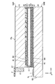


Classifications
-
- G—PHYSICS
- G02—OPTICS
- G02F—OPTICAL DEVICES OR ARRANGEMENTS FOR THE CONTROL OF LIGHT BY MODIFICATION OF THE OPTICAL PROPERTIES OF THE MEDIA OF THE ELEMENTS INVOLVED THEREIN; NON-LINEAR OPTICS; FREQUENCY-CHANGING OF LIGHT; OPTICAL LOGIC ELEMENTS; OPTICAL ANALOGUE/DIGITAL CONVERTERS
- G02F1/00—Devices or arrangements for the control of the intensity, colour, phase, polarisation or direction of light arriving from an independent light source, e.g. switching, gating or modulating; Non-linear optics
- G02F1/01—Devices or arrangements for the control of the intensity, colour, phase, polarisation or direction of light arriving from an independent light source, e.g. switching, gating or modulating; Non-linear optics for the control of the intensity, phase, polarisation or colour
- G02F1/13—Devices or arrangements for the control of the intensity, colour, phase, polarisation or direction of light arriving from an independent light source, e.g. switching, gating or modulating; Non-linear optics for the control of the intensity, phase, polarisation or colour based on liquid crystals, e.g. single liquid crystal display cells
- G02F1/133—Constructional arrangements; Operation of liquid crystal cells; Circuit arrangements
- G02F1/1333—Constructional arrangements; Manufacturing methods
- G02F1/133345—Insulating layers
-
- G—PHYSICS
- G02—OPTICS
- G02F—OPTICAL DEVICES OR ARRANGEMENTS FOR THE CONTROL OF LIGHT BY MODIFICATION OF THE OPTICAL PROPERTIES OF THE MEDIA OF THE ELEMENTS INVOLVED THEREIN; NON-LINEAR OPTICS; FREQUENCY-CHANGING OF LIGHT; OPTICAL LOGIC ELEMENTS; OPTICAL ANALOGUE/DIGITAL CONVERTERS
- G02F1/00—Devices or arrangements for the control of the intensity, colour, phase, polarisation or direction of light arriving from an independent light source, e.g. switching, gating or modulating; Non-linear optics
- G02F1/01—Devices or arrangements for the control of the intensity, colour, phase, polarisation or direction of light arriving from an independent light source, e.g. switching, gating or modulating; Non-linear optics for the control of the intensity, phase, polarisation or colour
- G02F1/13—Devices or arrangements for the control of the intensity, colour, phase, polarisation or direction of light arriving from an independent light source, e.g. switching, gating or modulating; Non-linear optics for the control of the intensity, phase, polarisation or colour based on liquid crystals, e.g. single liquid crystal display cells
- G02F1/133—Constructional arrangements; Operation of liquid crystal cells; Circuit arrangements
- G02F1/1333—Constructional arrangements; Manufacturing methods
- G02F1/1335—Structural association of cells with optical devices, e.g. polarisers or reflectors
-
- G—PHYSICS
- G02—OPTICS
- G02F—OPTICAL DEVICES OR ARRANGEMENTS FOR THE CONTROL OF LIGHT BY MODIFICATION OF THE OPTICAL PROPERTIES OF THE MEDIA OF THE ELEMENTS INVOLVED THEREIN; NON-LINEAR OPTICS; FREQUENCY-CHANGING OF LIGHT; OPTICAL LOGIC ELEMENTS; OPTICAL ANALOGUE/DIGITAL CONVERTERS
- G02F1/00—Devices or arrangements for the control of the intensity, colour, phase, polarisation or direction of light arriving from an independent light source, e.g. switching, gating or modulating; Non-linear optics
- G02F1/01—Devices or arrangements for the control of the intensity, colour, phase, polarisation or direction of light arriving from an independent light source, e.g. switching, gating or modulating; Non-linear optics for the control of the intensity, phase, polarisation or colour
- G02F1/13—Devices or arrangements for the control of the intensity, colour, phase, polarisation or direction of light arriving from an independent light source, e.g. switching, gating or modulating; Non-linear optics for the control of the intensity, phase, polarisation or colour based on liquid crystals, e.g. single liquid crystal display cells
- G02F1/133—Constructional arrangements; Operation of liquid crystal cells; Circuit arrangements
- G02F1/1333—Constructional arrangements; Manufacturing methods
- G02F1/1335—Structural association of cells with optical devices, e.g. polarisers or reflectors
- G02F1/133524—Light-guides, e.g. fibre-optic bundles, louvered or jalousie light-guides
-
- G—PHYSICS
- G02—OPTICS
- G02F—OPTICAL DEVICES OR ARRANGEMENTS FOR THE CONTROL OF LIGHT BY MODIFICATION OF THE OPTICAL PROPERTIES OF THE MEDIA OF THE ELEMENTS INVOLVED THEREIN; NON-LINEAR OPTICS; FREQUENCY-CHANGING OF LIGHT; OPTICAL LOGIC ELEMENTS; OPTICAL ANALOGUE/DIGITAL CONVERTERS
- G02F1/00—Devices or arrangements for the control of the intensity, colour, phase, polarisation or direction of light arriving from an independent light source, e.g. switching, gating or modulating; Non-linear optics
- G02F1/01—Devices or arrangements for the control of the intensity, colour, phase, polarisation or direction of light arriving from an independent light source, e.g. switching, gating or modulating; Non-linear optics for the control of the intensity, phase, polarisation or colour
- G02F1/13—Devices or arrangements for the control of the intensity, colour, phase, polarisation or direction of light arriving from an independent light source, e.g. switching, gating or modulating; Non-linear optics for the control of the intensity, phase, polarisation or colour based on liquid crystals, e.g. single liquid crystal display cells
- G02F1/133—Constructional arrangements; Operation of liquid crystal cells; Circuit arrangements
- G02F1/1333—Constructional arrangements; Manufacturing methods
- G02F1/1343—Electrodes
- G02F1/134309—Electrodes characterised by their geometrical arrangement
- G02F1/134336—Matrix
-
- G—PHYSICS
- G02—OPTICS
- G02B—OPTICAL ELEMENTS, SYSTEMS OR APPARATUS
- G02B6/00—Light guides; Structural details of arrangements comprising light guides and other optical elements, e.g. couplings
- G02B6/0001—Light guides; Structural details of arrangements comprising light guides and other optical elements, e.g. couplings specially adapted for lighting devices or systems
- G02B6/0011—Light guides; Structural details of arrangements comprising light guides and other optical elements, e.g. couplings specially adapted for lighting devices or systems the light guides being planar or of plate-like form
- G02B6/0081—Mechanical or electrical aspects of the light guide and light source in the lighting device peculiar to the adaptation to planar light guides, e.g. concerning packaging
- G02B6/0086—Positioning aspects
- G02B6/0091—Positioning aspects of the light source relative to the light guide
-
- G—PHYSICS
- G02—OPTICS
- G02F—OPTICAL DEVICES OR ARRANGEMENTS FOR THE CONTROL OF LIGHT BY MODIFICATION OF THE OPTICAL PROPERTIES OF THE MEDIA OF THE ELEMENTS INVOLVED THEREIN; NON-LINEAR OPTICS; FREQUENCY-CHANGING OF LIGHT; OPTICAL LOGIC ELEMENTS; OPTICAL ANALOGUE/DIGITAL CONVERTERS
- G02F1/00—Devices or arrangements for the control of the intensity, colour, phase, polarisation or direction of light arriving from an independent light source, e.g. switching, gating or modulating; Non-linear optics
- G02F1/01—Devices or arrangements for the control of the intensity, colour, phase, polarisation or direction of light arriving from an independent light source, e.g. switching, gating or modulating; Non-linear optics for the control of the intensity, phase, polarisation or colour
- G02F1/13—Devices or arrangements for the control of the intensity, colour, phase, polarisation or direction of light arriving from an independent light source, e.g. switching, gating or modulating; Non-linear optics for the control of the intensity, phase, polarisation or colour based on liquid crystals, e.g. single liquid crystal display cells
- G02F1/133—Constructional arrangements; Operation of liquid crystal cells; Circuit arrangements
- G02F1/1333—Constructional arrangements; Manufacturing methods
- G02F1/133342—Constructional arrangements; Manufacturing methods for double-sided displays
-
- G—PHYSICS
- G02—OPTICS
- G02F—OPTICAL DEVICES OR ARRANGEMENTS FOR THE CONTROL OF LIGHT BY MODIFICATION OF THE OPTICAL PROPERTIES OF THE MEDIA OF THE ELEMENTS INVOLVED THEREIN; NON-LINEAR OPTICS; FREQUENCY-CHANGING OF LIGHT; OPTICAL LOGIC ELEMENTS; OPTICAL ANALOGUE/DIGITAL CONVERTERS
- G02F1/00—Devices or arrangements for the control of the intensity, colour, phase, polarisation or direction of light arriving from an independent light source, e.g. switching, gating or modulating; Non-linear optics
- G02F1/01—Devices or arrangements for the control of the intensity, colour, phase, polarisation or direction of light arriving from an independent light source, e.g. switching, gating or modulating; Non-linear optics for the control of the intensity, phase, polarisation or colour
- G02F1/13—Devices or arrangements for the control of the intensity, colour, phase, polarisation or direction of light arriving from an independent light source, e.g. switching, gating or modulating; Non-linear optics for the control of the intensity, phase, polarisation or colour based on liquid crystals, e.g. single liquid crystal display cells
- G02F1/133—Constructional arrangements; Operation of liquid crystal cells; Circuit arrangements
- G02F1/1333—Constructional arrangements; Manufacturing methods
- G02F1/1334—Constructional arrangements; Manufacturing methods based on polymer dispersed liquid crystals, e.g. microencapsulated liquid crystals
- G02F1/13347—Constructional arrangements; Manufacturing methods based on polymer dispersed liquid crystals, e.g. microencapsulated liquid crystals working in reverse mode, i.e. clear in the off-state and scattering in the on-state
-
- G—PHYSICS
- G02—OPTICS
- G02F—OPTICAL DEVICES OR ARRANGEMENTS FOR THE CONTROL OF LIGHT BY MODIFICATION OF THE OPTICAL PROPERTIES OF THE MEDIA OF THE ELEMENTS INVOLVED THEREIN; NON-LINEAR OPTICS; FREQUENCY-CHANGING OF LIGHT; OPTICAL LOGIC ELEMENTS; OPTICAL ANALOGUE/DIGITAL CONVERTERS
- G02F1/00—Devices or arrangements for the control of the intensity, colour, phase, polarisation or direction of light arriving from an independent light source, e.g. switching, gating or modulating; Non-linear optics
- G02F1/01—Devices or arrangements for the control of the intensity, colour, phase, polarisation or direction of light arriving from an independent light source, e.g. switching, gating or modulating; Non-linear optics for the control of the intensity, phase, polarisation or colour
- G02F1/13—Devices or arrangements for the control of the intensity, colour, phase, polarisation or direction of light arriving from an independent light source, e.g. switching, gating or modulating; Non-linear optics for the control of the intensity, phase, polarisation or colour based on liquid crystals, e.g. single liquid crystal display cells
- G02F1/133—Constructional arrangements; Operation of liquid crystal cells; Circuit arrangements
- G02F1/1333—Constructional arrangements; Manufacturing methods
- G02F1/1335—Structural association of cells with optical devices, e.g. polarisers or reflectors
- G02F1/133502—Antiglare, refractive index matching layers
-
- G—PHYSICS
- G02—OPTICS
- G02F—OPTICAL DEVICES OR ARRANGEMENTS FOR THE CONTROL OF LIGHT BY MODIFICATION OF THE OPTICAL PROPERTIES OF THE MEDIA OF THE ELEMENTS INVOLVED THEREIN; NON-LINEAR OPTICS; FREQUENCY-CHANGING OF LIGHT; OPTICAL LOGIC ELEMENTS; OPTICAL ANALOGUE/DIGITAL CONVERTERS
- G02F1/00—Devices or arrangements for the control of the intensity, colour, phase, polarisation or direction of light arriving from an independent light source, e.g. switching, gating or modulating; Non-linear optics
- G02F1/01—Devices or arrangements for the control of the intensity, colour, phase, polarisation or direction of light arriving from an independent light source, e.g. switching, gating or modulating; Non-linear optics for the control of the intensity, phase, polarisation or colour
- G02F1/13—Devices or arrangements for the control of the intensity, colour, phase, polarisation or direction of light arriving from an independent light source, e.g. switching, gating or modulating; Non-linear optics for the control of the intensity, phase, polarisation or colour based on liquid crystals, e.g. single liquid crystal display cells
- G02F1/133—Constructional arrangements; Operation of liquid crystal cells; Circuit arrangements
- G02F1/1333—Constructional arrangements; Manufacturing methods
- G02F1/1335—Structural association of cells with optical devices, e.g. polarisers or reflectors
- G02F1/133509—Filters, e.g. light shielding masks
- G02F1/133512—Light shielding layers, e.g. black matrix
-
- G—PHYSICS
- G02—OPTICS
- G02F—OPTICAL DEVICES OR ARRANGEMENTS FOR THE CONTROL OF LIGHT BY MODIFICATION OF THE OPTICAL PROPERTIES OF THE MEDIA OF THE ELEMENTS INVOLVED THEREIN; NON-LINEAR OPTICS; FREQUENCY-CHANGING OF LIGHT; OPTICAL LOGIC ELEMENTS; OPTICAL ANALOGUE/DIGITAL CONVERTERS
- G02F1/00—Devices or arrangements for the control of the intensity, colour, phase, polarisation or direction of light arriving from an independent light source, e.g. switching, gating or modulating; Non-linear optics
- G02F1/01—Devices or arrangements for the control of the intensity, colour, phase, polarisation or direction of light arriving from an independent light source, e.g. switching, gating or modulating; Non-linear optics for the control of the intensity, phase, polarisation or colour
- G02F1/13—Devices or arrangements for the control of the intensity, colour, phase, polarisation or direction of light arriving from an independent light source, e.g. switching, gating or modulating; Non-linear optics for the control of the intensity, phase, polarisation or colour based on liquid crystals, e.g. single liquid crystal display cells
- G02F1/133—Constructional arrangements; Operation of liquid crystal cells; Circuit arrangements
- G02F1/1333—Constructional arrangements; Manufacturing methods
- G02F1/1335—Structural association of cells with optical devices, e.g. polarisers or reflectors
- G02F1/1336—Illuminating devices
- G02F1/133616—Front illuminating devices
-
- G—PHYSICS
- G02—OPTICS
- G02F—OPTICAL DEVICES OR ARRANGEMENTS FOR THE CONTROL OF LIGHT BY MODIFICATION OF THE OPTICAL PROPERTIES OF THE MEDIA OF THE ELEMENTS INVOLVED THEREIN; NON-LINEAR OPTICS; FREQUENCY-CHANGING OF LIGHT; OPTICAL LOGIC ELEMENTS; OPTICAL ANALOGUE/DIGITAL CONVERTERS
- G02F1/00—Devices or arrangements for the control of the intensity, colour, phase, polarisation or direction of light arriving from an independent light source, e.g. switching, gating or modulating; Non-linear optics
- G02F1/01—Devices or arrangements for the control of the intensity, colour, phase, polarisation or direction of light arriving from an independent light source, e.g. switching, gating or modulating; Non-linear optics for the control of the intensity, phase, polarisation or colour
- G02F1/13—Devices or arrangements for the control of the intensity, colour, phase, polarisation or direction of light arriving from an independent light source, e.g. switching, gating or modulating; Non-linear optics for the control of the intensity, phase, polarisation or colour based on liquid crystals, e.g. single liquid crystal display cells
- G02F1/133—Constructional arrangements; Operation of liquid crystal cells; Circuit arrangements
- G02F1/1333—Constructional arrangements; Manufacturing methods
- G02F1/1337—Surface-induced orientation of the liquid crystal molecules, e.g. by alignment layers
- G02F1/133738—Surface-induced orientation of the liquid crystal molecules, e.g. by alignment layers for homogeneous alignment
-
- G—PHYSICS
- G02—OPTICS
- G02F—OPTICAL DEVICES OR ARRANGEMENTS FOR THE CONTROL OF LIGHT BY MODIFICATION OF THE OPTICAL PROPERTIES OF THE MEDIA OF THE ELEMENTS INVOLVED THEREIN; NON-LINEAR OPTICS; FREQUENCY-CHANGING OF LIGHT; OPTICAL LOGIC ELEMENTS; OPTICAL ANALOGUE/DIGITAL CONVERTERS
- G02F2202/00—Materials and properties
- G02F2202/02—Materials and properties organic material
- G02F2202/022—Materials and properties organic material polymeric
-
- G—PHYSICS
- G02—OPTICS
- G02F—OPTICAL DEVICES OR ARRANGEMENTS FOR THE CONTROL OF LIGHT BY MODIFICATION OF THE OPTICAL PROPERTIES OF THE MEDIA OF THE ELEMENTS INVOLVED THEREIN; NON-LINEAR OPTICS; FREQUENCY-CHANGING OF LIGHT; OPTICAL LOGIC ELEMENTS; OPTICAL ANALOGUE/DIGITAL CONVERTERS
- G02F2202/00—Materials and properties
- G02F2202/40—Materials having a particular birefringence, retardation
Definitions
- the embodiment of the present invention relates to a display device.
- a lighting device including a light modulating layer including optically anisotropic bulk and fine particles in a light modulating element bonded to a light guide plate.
- a light source device that includes a polymer-dispersed liquid crystal and includes a light conversion unit that converts the intensity of incident light is disclosed.
- the object of the present embodiment is to provide a display device capable of suppressing a decrease in display quality.
- a first transparent substrate having a side surface and a main surface, a first alignment film disposed along the main surface, a first transparent layer located between the first transparent substrate and the first alignment film, A first substrate, a second transparent substrate, a scanning line, a signal line crossing the scanning line, a switching element electrically connected to the scanning line and the signal line, and a switching element; A second substrate having a pixel electrode electrically connected thereto, a liquid crystal layer held between the first substrate and the second substrate and containing a streak-like polymer and liquid crystal molecules, And a light emitting element facing the light emitting element, wherein the first transparent layer overlaps a part of the pixel electrode and has a lower refractive index than the first transparent substrate.
- a first substrate having a first transparent substrate having a side surface and a main surface, and a first alignment film disposed along the main surface; a second transparent substrate; a scanning line; and an intersection with the scanning line.
- a second substrate having a second transparent layer positioned between the switching element and the second alignment film; and a streak-like polymer held between the first substrate and the second substrate.
- a liquid crystal layer containing liquid crystal molecules, and a light emitting element facing the side surface, wherein the second transparent layer overlaps the pixel electrode and has a lower refractive index than the first transparent substrate.
- the first substrate comprises: a first transparent substrate having a side surface facing the light emitting element; a first alignment film in contact with the liquid crystal layer; and a first transparent substrate and the first alignment film.
- the first transparent layer and the second transparent layer are insulating layers, and the installation area per pixel of the first transparent layer is equal to or less than the second transparent layer.
- a display device having a smaller installation area per pixel is provided.
- FIG. 1 is a plan view illustrating a configuration example of the display device DSP according to the present embodiment.
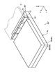
- FIG. 2 is a perspective view showing a main part of the display device DSP shown in FIG.
- FIG. 3 is a cross-sectional view showing one configuration example of the display panel PNL shown in FIG.
- FIG. 4 is a plan view showing a configuration example of the display panel PNL shown in FIG.
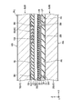
- FIG. 5 is a cross-sectional view illustrating a configuration example of the display device DSP of the present embodiment.
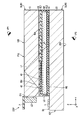
- FIG. 6 is a cross-sectional view illustrating another configuration example of the display device DSP illustrated in FIG.
- FIG. 7 is a cross-sectional view illustrating another configuration example of the display device DSP illustrated in FIG.
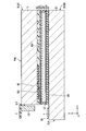
- FIG. 8 is a sectional view showing another configuration example of the display device DSP shown in FIG.
- FIG. 9 is a plan view showing another configuration example of the transparent layer 40 shown in FIG.
- FIG. 10 is a plan view showing another configuration example of the transparent layer 40
- FIG. 1 is a plan view showing one configuration example of the display device DSP of the present embodiment.
- the first direction X, the second direction Y, and the third direction Z are orthogonal to each other, but may intersect at an angle other than 90 degrees.
- the first direction X and the second direction Y correspond to directions parallel to the main surface of the substrate constituting the display device DSP
- the third direction Z corresponds to the thickness direction of the display device DSP.
- the direction from the second substrate SUB2 to the first substrate SUB1 is referred to as “upper” (or simply upper), and the direction from the first substrate SUB1 to the second substrate SUB2 is “lower” (or Simply below).
- the second member may be in contact with the first member or may be separated from the first member. You may. Further, it is assumed that there is an observation position for observing the display device DSP on the tip side of the arrow indicating the third direction Z, and from this observation position, an XY plane defined by the first direction X and the second direction Y is provided. Viewing is called planar view.
- the display device DSP includes a display panel PNL, an IC chip 1, and a wiring board 2.
- the display panel PNL includes a first substrate SUB1, a second substrate SUB2, a liquid crystal layer LC, and a seal SE.
- the first substrate SUB1 and the second substrate SUB2 are formed in a flat plate shape parallel to the XY plane.
- the first substrate SUB1 and the second substrate SUB2 overlap in plan view.
- the first substrate SUB1 and the second substrate SUB2 are bonded by a seal SE.
- the liquid crystal layer LC is held between the first substrate SUB1 and the second substrate SUB2, and is sealed by a seal SE.
- the liquid crystal layer LC and the seal SE are indicated by different oblique lines.
- the liquid crystal layer LC includes a polymer-dispersed liquid crystal including a polymer 31 and liquid crystal molecules 32.
- the polymer 31 is a liquid crystalline polymer.
- the polymer 31 is formed in a streak shape extending along the first direction X.
- the liquid crystal molecules 32 are dispersed in the gaps between the polymers 31, and are oriented such that their major axes are along the first direction X.
- Each of the polymer 31 and the liquid crystal molecules 32 has optical anisotropy or refractive index anisotropy.
- the response of the polymer 31 to the electric field is lower than the response of the liquid crystal molecules 32 to the electric field.
- the orientation direction of the polymer 31 hardly changes regardless of the presence or absence of an electric field.
- the orientation direction of the liquid crystal molecules 32 changes according to the electric field when a high voltage equal to or higher than the threshold is applied to the liquid crystal layer LC.
- a high voltage equal to or higher than the threshold is applied to the liquid crystal layer LC.
- the optical axes of the polymer 31 and the liquid crystal molecules 32 are parallel to each other, and the light incident on the liquid crystal layer LC is hardly scattered in the liquid crystal layer LC. Transmit (transparent state).
- the respective optical axes of the polymer 31 and the liquid crystal molecules 32 cross each other, and the light incident on the liquid crystal layer LC is scattered in the liquid crystal layer LC (scattered state).
- the display panel PNL includes a display section DA for displaying an image, and a frame-shaped non-display section NDA surrounding the display section DA.
- the seal SE is located in the non-display portion NDA.
- the display section DA includes pixels PX arranged in a matrix in the first direction X and the second direction Y.
- each pixel PX includes a switching element SW, a pixel electrode PE, a common electrode CE, a liquid crystal layer LC, and the like.
- the switching element SW is composed of, for example, a thin film transistor (TFT), and is electrically connected to the scanning line G and the signal line S.
- the scanning line G is electrically connected to the switching element SW in each of the pixels PX arranged in the first direction X.
- the signal line S is electrically connected to the switching element SW in each of the pixels PX arranged in the second direction Y.
- the pixel electrode PE is electrically connected to the switching element SW.
- Each of the pixel electrodes PE faces the common electrode CE, and drives the liquid crystal layer LC (particularly, the liquid crystal molecules 32) by an electric field generated between the pixel electrode PE and the common electrode CE.
- the capacitor CS is formed, for example, between an electrode having the same potential as the common electrode CE and an electrode having the same potential as the pixel electrode PE.
- the second substrate SUB2 has the extension Ex.
- the extension Ex corresponds to a region where the second substrate SUB2 does not overlap the first substrate SUB1.
- the IC chip 1 and the wiring board 2 are connected to the extension Ex, respectively.
- the IC chip 1 includes, for example, a display driver that outputs a signal necessary for image display.
- the wiring board 2 is a bendable flexible printed circuit board. Note that the IC chip 1 may be connected to the wiring board 2. Although the IC chip 1 and the wiring board 2 may read a signal from the display panel PNL in some cases, the IC chip 1 and the wiring board 2 mainly function as a signal source for supplying a signal to the display panel PNL.
- FIG. 2 is a perspective view showing a main part of the display device DSP shown in FIG.
- the display device DSP includes a plurality of light emitting elements LD in addition to the display panel PNL.
- the first substrate SUB1 and the second substrate SUB2 have transparent substrates 10 and 20, respectively.
- the transparent substrates 10 and 20 have side surfaces E11 and E21, respectively.
- the side surfaces E11 and E21 extend along the first direction X, and do not overlap in the third direction Z.
- the extension Ex extends in the second direction Y between the side surface E11 and the side surface E21.
- the plurality of light emitting elements LD are arranged at intervals in the first direction X and face the side surface E11. In the illustrated example, the plurality of light emitting elements LD overlap the extension Ex.
- the plurality of light emitting elements LD are connected to the wiring board F.
- the light emitting element LD is, for example, a light emitting diode.
- the light emitting element LD includes a red light emitting unit, a green light emitting unit, and a blue light emitting unit. Light emitted from the light emitting element LD travels along the direction of the arrow indicating the second direction Y.
- FIG. 3 is a cross-sectional view showing one configuration example of the display panel PNL shown in FIG.
- the second substrate SUB2 includes a transparent substrate 20, insulating films 21 and 22, a capacitor electrode 23, a switching element SW, a pixel electrode PE, a transparent layer 30, and an alignment film AL2.
- the second substrate SUB2 further includes the scanning lines G and the signal lines S illustrated in FIG.
- the transparent substrate 20 has a main surface (lower surface) 20A and a main surface (upper surface) 20B opposite to the main surface 20A.
- the main surfaces 20A and 20B are surfaces substantially parallel to the XY plane.
- Switching element SW is arranged on main surface 20B.
- the insulating film 21 covers the switching element SW.
- the capacitance electrode 23 is located between the insulating films 21 and 22.
- the pixel electrode PE is arranged on the insulating film 22 for each pixel PX.
- the pixel electrode PE is electrically connected to the switching element SW via the opening OP of the capacitance electrode 23.
- the pixel electrode PE overlaps with the capacitor electrode 23 with the insulating film 22 interposed therebetween to form the capacitor CS of the pixel PX.
- the transparent layer 30 is provided continuously without interruption along the first direction X, and covers the plurality of pixel electrodes PE.
- the alignment film AL2 covers the transparent layer 30.
- the transparent layer 30 is provided over the entire area of the pixel PX, is located between the pixel electrode PE and the alignment film AL2, and is in contact with both the pixel electrode PE and the alignment film AL2.
- the transparent layer 30 is in contact with the insulating film 22 between the pixel electrodes PE adjacent in the first direction X.
- another insulating layer or another conductive layer may be disposed between the transparent layer 30 and the pixel electrode PE and between the transparent layer 30 and the alignment film AL2.
- the transparent layer 30 is not limited to the illustrated example, and may be located between the transparent substrate 20 and the alignment film AL2 or between the switching element SW and the alignment film AL2.
- the first substrate SUB1 includes the transparent substrate 10, the light-shielding layer BM, the common electrode CE, the transparent layer 40, and the alignment film AL1.
- the transparent substrate 10 has a main surface (lower surface) 10A and a main surface (upper surface) 10B opposite to the main surface 10A.
- the main surfaces 10A and 10B are surfaces substantially parallel to the XY plane.
- the main surface 10A of the transparent substrate 10 faces the main surface 20B of the transparent substrate 20.
- the light shielding layer BM and the common electrode CE are arranged on the main surface 10A.
- the light shielding layer BM is located, for example, immediately above the switching element SW and immediately above the scanning line G and the signal line S (not shown).
- the common electrode CE is arranged over a plurality of pixels PX, and directly covers the light shielding layer BM.
- the common electrode CE is electrically connected to the capacitor electrode 23, and has the same potential as the capacitor electrode 23.
- the transparent layer 40 is partially provided below the common electrode CE and overlaps a part of the pixel electrode PE.
- the alignment film AL1 covers the transparent layer 40 and covers the common electrode CE in a portion where the transparent layer 40 is not provided. In the illustrated example, the transparent layer 40 is located between the common electrode CE and the alignment film AL1 in the region on the right side of the pixel PX, and is in contact with both the common electrode CE and the alignment film AL1.
- insulating layer or another conductive layer may be disposed between the transparent layer 40 and the common electrode CE and between the transparent layer 40 and the alignment film AL1.
- the transparent layer 40 is not limited to the illustrated example, and may be located between the transparent substrate 10 and the alignment film AL1.
- the liquid crystal layer LC is located between the first substrate SUB1 and the second substrate SUB2, and is in contact with each of the alignment films AL1 and AL2.
- the transparent substrates 10 and 20 are insulating substrates such as a glass substrate and a plastic substrate.
- the insulating film 21 is formed of a transparent insulating material such as silicon oxide, silicon nitride, silicon oxynitride, and acrylic resin.
- the insulating film 21 includes an inorganic insulating film and an organic insulating film.
- the insulating film 22 is an inorganic insulating film such as a silicon nitride.
- the capacitor electrode 23, the pixel electrode PE, and the common electrode CE are transparent electrodes formed of a transparent conductive material such as indium tin oxide (ITO) or indium zinc oxide (IZO).
- the light shielding layer BM is, for example, a conductive layer having a lower resistance than the common electrode CE.
- the light shielding layer BM is formed of an opaque metal material such as molybdenum, aluminum, tungsten, titanium, and silver.
- the transparent layers 30 and 40 are insulating layers formed of, for example, an organic material such as a siloxane-based resin or a fluorine-based resin.
- the alignment films AL1 and AL2 are horizontal alignment films having an alignment control force substantially parallel to the XY plane. In one example, the alignment films AL1 and AL2 are aligned along the first direction X. Note that the alignment treatment may be a rubbing treatment or a photo-alignment treatment.
- the transparent substrates 10 and 20 have refractive indices n10 and n20.
- the transparent layers 30 and 40 have refractive indices n30 and n40.
- the refractive indices n30 and n40 are lower than the refractive indices n10 and n20.
- the transparent layers 30 and 40 are formed of the same material, and have the same refractive index n30 and n40.
- “equivalent” includes not only a case where the refractive index difference is zero but also a case where the refractive index difference is 0.03 or less.
- the refractive indices n10 and n20 are about 1.5, and the refractive indices n30 and n40 are 1.0 or more and 1.41 or less.
- the main surface 10B of the transparent substrate 10 is in contact with air.
- another transparent layer having the same refractive index as the transparent layer 40 is disposed on the entire main surface 10B.
- another transparent layer having the same refractive index as that of the transparent layer 30 may be disposed on the entire main surface 20 ⁇ / b> A of the transparent substrate 20.
- FIG. 4 is a plan view showing a configuration example of the display panel PNL shown in FIG.
- the scanning lines G1 to G3 extend in the first direction X and are arranged at intervals in the second direction Y.
- the signal lines S1 to S3 extend in the second direction Y and are arranged at intervals in the first direction X.
- Each of the pixels PX1 to PX4 corresponds to an area defined by the scanning lines G1 to G3 and the signal lines S1 to S3.
- the pixels PX1 and PX3 are adjacent in the first direction X, and are closer to the light emitting element LD than the pixels PX2 and PX4.
- the pixel PX1 includes a switching element SW1 and a pixel electrode PE1.
- the pixels PX2 to PX4 include switching elements SW2 to SW4 and pixel electrodes PE2 to PE4, respectively.
- the pixel electrodes PE1 and PE2 are arranged at intervals along the second direction Y.
- the pixel electrodes PE1 and PE3 are arranged at intervals along the first direction X.
- the pixel electrodes PE1 and PE3 are close to the light emitting element LD, and the pixel electrodes PE2 and PE4 are separated from the light emitting element LD.
- the transparent layer 30 is provided continuously over the pixels PX1 to PX4. That is, the transparent layer 30 overlaps the scanning lines G1 to G3, the signal lines S1 to S3, the switching elements SW1 to SW4, and the pixel electrodes PE1 to PE4. Although not described in detail, the transparent layer 30 is provided over the entire area of the display section DA on the second substrate SUB2.
- the transparent layer 40 has transparent layers 41 to 44 provided in the pixels PX1 to PX4, respectively.
- the transparent layers 41 to 44 are each formed in an island shape extending along the second direction Y and are separated from each other.
- the transparent layers 41 and 43 are arranged at an interval IV1 in the first direction X
- the transparent layers 42 and 44 are arranged at an interval IV2 in the first direction X.
- the interval IV1 is smaller than the interval IV2.
- the transparent layers 41 and 42 are arranged at intervals in the second direction Y
- the transparent layers 43 and 44 are arranged at intervals in the second direction Y. Note that the transparent layers 41 and 42 may be formed continuously, and similarly, the transparent layers 43 and 44 may be formed continuously.
- the transparent layer 41 overlaps the pixel electrode PE1, and the transparent layer 42 overlaps the pixel electrode PE2.
- the transparent layer 41 has a larger area than the transparent layer 42. Therefore, the area where the transparent layer 41 overlaps with the pixel electrode PE1 is larger than the area where the transparent layer 42 overlaps with the pixel electrode PE2.
- the transparent layers 43 and 44 overlap the pixel electrodes PE3 and PE4, respectively.
- the area where the transparent layer 41 overlaps the pixel electrode PE1 is equal to the area where the transparent layer 43 overlaps the pixel electrode PE3, and the area where the transparent layer 42 overlaps the pixel electrode PE2 is where the transparent layer 44 overlaps the pixel electrode PE4. It is equivalent to the area.
- the installation area per pixel is defined as an area overlapping the pixel electrode PE in a plan view, for example, in the first pixel PX1, the transparent layer 30 overlaps almost the entire pixel electrode PE1, The transparent layer 41 overlaps a part of the pixel electrode PE1, and the installation area of the transparent layer 41 is smaller than the installation area of the transparent layer 30.
- the other pixels PX2 to PX4 are defined as an area overlapping the pixel electrode PE in a plan view, for example, in the first pixel PX1, the transparent layer 30 overlaps almost the entire pixel electrode PE1, The transparent layer 41 overlaps a part of the pixel electrode PE1, and the installation area of the transparent layer 41 is smaller than the installation area of the transparent layer 30. The same applies to the other pixels PX2 to PX4.
- the light shielding layer BM is formed in a lattice shape.
- the light-blocking layer BM overlaps the scanning lines G1 to G3, the signal lines S1 to S3, and the switching elements SW1 to S4.
- the light-shielding layer BM overlaps a pair of ends E1 of the transparent layer 41, a pair of ends E2 of the transparent layer 42, a pair of ends E3 of the transparent layer 43, and a pair of ends E4 of the transparent layer 44. are doing. These ends E1 to E4 are ends extending along the first direction X.
- FIG. 5 is a cross-sectional view illustrating a configuration example of the display device DSP of the present embodiment. Note that only the main part of the display panel PNL is illustrated.
- the light emitted from the light emitting element LD will be described with reference to FIG.
- the light emitting element LD emits the light L1 toward the side surface E11. Since an air layer exists between the light emitting element LD and the side surface E11, the light L1 emitted from the light emitting element LD is refracted at the side surface E11 and enters the transparent substrate 10. Of the light L1 incident on the transparent substrate 10, the light traveling toward the main surface 10B is reflected at the interface between the transparent substrate 10 and the air layer.
- the light traveling toward the light shielding layer BM is reflected by the light shielding layer BM.
- the light traveling toward the transparent layer 40 is reflected at the interface between the common electrode CE and the transparent layer 40, and is aligned with the alignment film AL1, the liquid crystal layer LC, and the second substrate. It does not reach SUB2.
- the light L1 travels inside the transparent substrate 10 while being repeatedly reflected near the side surface E11 (or in a region where the transparent layer 40 is present).
- the traveling light L1 light traveling toward a region where the transparent layer 40 does not exist, that is, a region where the common electrode CE and the alignment film AL1 are in contact with each other enters the liquid crystal layer LC.
- the installation area per pixel of the transparent layer 40 is smaller in a region close to the light emitting element LD than in a region separated from the light emitting element LD. Therefore, in a region close to the light emitting element LD, the incidence of the light L1 from the light emitting element LD on the liquid crystal layer LC is suppressed, while in a region separated from the light emitting element LD, the light L1 Incident on the substrate is promoted. Note that, in the region close to the light emitting element LD, the light L1 does not necessarily enter the liquid crystal layer LC at all, and as shown in FIG. 4, the light L1 is supplied from the region where the transparent layer 40 does not overlap the pixel electrode PE. Light is incident on the layer LC.
- the display device DSP can be observed from the observation position VP1 on the main surface 10B side and also from the observation position VP2 on the main surface 20A side.
- the display device DSP can observe the background of the display device DSP via the display device DSP regardless of whether the display device DSP is observed from the observation position VP1 or the observation position VP2.
- the light traveling inside the transparent substrate 10 does not enter the alignment film AL1 and proceeds inside the transparent substrate 10 as it is.
- undesired absorption and scattering in the alignment films AL1 and AL2 can be suppressed, and a decrease in the efficiency of using light from the light emitting element LD can be suppressed.
- the luminance tends to sharply decrease when separated from the light emitting element LD.
- One cause of such a decrease in brightness is undesired absorption. Therefore, by suppressing absorption in the alignment films AL1 and AL2, it is possible to suppress a decrease in luminance.
- the pixel electrode PE, the capacitor electrode 23, the switching element SW, the signal line S, and the scanning line G are located between the transparent layer 30 and the transparent substrate 20.
- the pixel electrode PE, the capacitor electrode 23, the switching element SW, Unwanted absorption and scattering at the signal line S and the scanning line G are suppressed. Therefore, according to the present embodiment, a decrease in display quality can be suppressed.
- a region where the transparent layer 40 overlaps the pixel electrode PE corresponds to a region where light from the light emitting element LD hardly enters the alignment film AL1 and the liquid crystal layer LC, and a region where the transparent layer 40 does not overlap the pixel electrode PE ( Alternatively, the region between the adjacent transparent layers 40) corresponds to a region where light from the light emitting element LD enters the liquid crystal layer LC via the alignment film AL1. In the region close to the light emitting element LD, the installation area per pixel of the transparent layer 40 is smaller than in the region separated from the light emitting element LD.
- the light from the light emitting element LD attenuates as the distance from the light emitting element LD increases.
- the luminance of light in a region close to the light emitting element LD is referred to as a first luminance
- the luminance of light in a region separated from the light emitting element LD is referred to as a second luminance.
- the second luminance is lower than the first luminance.
- the illumination light amounts in the pixels PX1 and PX2 can be equalized.
- the transparent substrate 10 corresponds to a first transparent substrate
- the alignment film AL1 corresponds to a first alignment film
- the transparent layer 40 corresponds to a first transparent layer
- the transparent substrate 20 corresponds to a second transparent substrate
- the transparent layer 30 corresponds to a second transparent layer
- the alignment film AL2 corresponds to a second alignment film
- the pixel electrode PE1 corresponds to a first pixel electrode
- the pixel electrode PE2 It corresponds to a second pixel electrode.
- the scanning line G, the signal line S, the switching element SW, and the pixel electrode PE may be provided on the first substrate SUB1, and the common electrode CE may be provided on the second substrate SUB2.
- FIG. 6 is a cross-sectional view illustrating another configuration example of the display device DSP illustrated in FIG.
- the configuration example shown in FIG. 6 is different from the configuration example shown in FIG. 5 in that the first substrate SUB1 includes an insulating film 50.
- the transparent layer 40 is formed on the main surface 10 ⁇ / b> A and is covered with the insulating film 50.
- the common electrode CE is located below the insulating film 50 and is covered by the alignment film AL1.
- the insulating film 50 is, for example, an organic insulating film formed of an organic material such as an acrylic resin. The lower surface of the insulating film 50 in contact with the common electrode CE is flattened.
- the transparent layer 40 is located between the common electrode CE and the transparent substrate 10.
- the same effect as in the configuration example shown in FIG. 5 can be obtained.
- the transparent layer 40 is located between the transparent substrate 10 and the common electrode CE, the transparent layer 40 is more common than when the transparent layer 40 is located between the common electrode CE and the alignment film AL1.
- the electrode CE approaches the pixel electrode PE along the third direction Z, and it is possible to suppress a decrease in the electric field strength between the pixel electrode PE and the common electrode CE.
- FIG. 7 is a cross-sectional view illustrating another configuration example of the display device DSP illustrated in FIG.
- the configuration example shown in FIG. 7 is different from the configuration example shown in FIG. 5 in that the pixel electrode PE is formed on the transparent layer 30.
- the transparent layer 30 is located between the switching element SW and the pixel electrode PE.
- the same effect as in the configuration example shown in FIG. 5 can be obtained.
- the transparent layer 30 is located between the transparent substrate 20 and the pixel electrode PE, compared with the case where the transparent layer 30 is located between the pixel electrode PE and the alignment film AL2, the pixel The electrode PE approaches the common electrode CE along the third direction Z, and it is possible to suppress a decrease in the electric field strength between the pixel electrode PE and the common electrode CE.
- the insulating film 21 is located between the transparent substrate 20 and the transparent layer 30 in the illustrated example, the insulating film 21 may be omitted.
- FIG. 8 is a sectional view showing another configuration example of the display device DSP shown in FIG.
- the configuration example shown in FIG. 8 corresponds to an example in which the first substrate SUB1 shown in FIG. 6 and the second substrate SUB2 shown in FIG. 7 are combined.
- the same effect as in the configuration example shown in FIG. 5 can be obtained.
- the transparent layer 30 and the transparent layer 40 are not located between the pixel electrode PE and the common electrode CE, the common electrode CE and the pixel electrode PE approach in the third direction Z, and the pixel electrode PE And the common electrode CE can be further suppressed from decreasing in electric field strength.
- FIG. 9 is a plan view showing another configuration example of the transparent layer 40 shown in FIG.
- the configuration example shown in FIG. 9 is different from the configuration example shown in FIG. 4 in that the transparent layers 43 and 44 are close to the signal line S2.
- the transparent layers 41 to 44 may be formed continuously.
- FIG. 10 is a plan view showing another configuration example of the transparent layer 40 shown in FIG.
- the configuration example shown in FIG. 10 is different from the configuration example shown in FIG. 4 in that the transparent layer 41 is close to the signal line S1 and the transparent layer 44 is close to the signal line S2. .
- the transparent layers 42 and 44 may be formed continuously. Also in the configuration examples shown in FIGS. 9 and 10, the same effects as described above can be obtained.
- a first transparent substrate having a side surface and a main surface, a first alignment film disposed along the main surface, a first transparent layer located between the first transparent substrate and the first alignment film,
- a first substrate comprising: A second transparent substrate, a scanning line, a signal line intersecting the scanning line, a switching element electrically connected to the scanning line and the signal line, and a pixel electrode electrically connected to the switching element.
- a second substrate comprising: A liquid crystal layer held between the first substrate and the second substrate and including a streak-like polymer and liquid crystal molecules; A light-emitting element facing the side surface, The display device, wherein the first transparent layer overlaps a part of the pixel electrode and has a lower refractive index than the first transparent substrate.
- the first substrate further includes a common electrode facing the pixel electrode, The display device according to (1) or (2), wherein the first transparent layer is located between the common electrode and the first alignment film.
- the first substrate further includes a common electrode facing the pixel electrode, The display device according to (1) or (2), wherein the first transparent layer is located between the common electrode and the first transparent substrate.
- the second substrate further includes a second alignment film in contact with the liquid crystal layer, and a second transparent layer located between the switching element and the second alignment film,
- the display device according to any one of (1) to (4), wherein the second transparent layer has a refractive index equivalent to that of the first transparent layer.
- a first substrate having a first transparent substrate having a side surface and a main surface, and a first alignment film disposed along the main surface; A second transparent substrate, a scanning line, a signal line intersecting the scanning line, a switching element electrically connected to the scanning line and the signal line, and a pixel electrode electrically connected to the switching element.
- a second substrate comprising: a second alignment film located on the pixel electrode; and a second transparent layer located between the switching element and the second alignment film.
- a liquid crystal layer held between the first substrate and the second substrate and including a streak-like polymer and liquid crystal molecules; A light-emitting element facing the side surface, The display device, wherein the second transparent layer overlaps the pixel electrode and has a lower refractive index than the first transparent substrate.
- the first substrate has a first transparent substrate having a side surface facing the light emitting element, a first alignment film in contact with the liquid crystal layer, and a first alignment film located between the first transparent substrate and the first alignment film.
- the second substrate includes a second transparent substrate, a second alignment film in contact with the liquid crystal layer, and a second transparent layer located between the second transparent substrate and the second alignment film,
- the first transparent layer and the second transparent layer are insulating layers,
- the display device wherein an installation area per pixel of the first transparent layer is smaller than an installation area per pixel of the second transparent layer.
- the second substrate further includes a first pixel electrode arranged in a first pixel close to the light emitting element, and a second pixel electrode arranged in a second pixel separated from the light emitting element,
- the first substrate further includes a common electrode facing the first pixel electrode and the second pixel electrode, The display device according to (10), wherein the first transparent layer is located between the common electrode and the first alignment film.
- the first substrate further includes a common electrode facing the first pixel electrode and the second pixel electrode, The display device according to (10), wherein the first transparent layer is located between the common electrode and the first transparent substrate.
- the second substrate further includes a scanning line, a signal line intersecting the scanning line, a switching element electrically connected to the scanning line and the signal line, and a pixel electrically connected to the switching element. And an electrode, The display device according to (9), wherein the scanning line, the signal line, and the switching element are located between the second transparent substrate and the second transparent layer.
- the side surface extends along a first direction
- the display device according to (9) wherein the first transparent layers are arranged at intervals along the first direction.
- DSP display device PNL: display panel 10
- 20 transparent substrate
- G scanning line
- S signal line
- SW switching element
- PE pixel electrode
- CE common electrode
- BM light shielding layer
- n Refractive index
Landscapes
- Physics & Mathematics (AREA)
- Nonlinear Science (AREA)
- Mathematical Physics (AREA)
- Chemical & Material Sciences (AREA)
- Crystallography & Structural Chemistry (AREA)
- General Physics & Mathematics (AREA)
- Optics & Photonics (AREA)
- Geometry (AREA)
- Liquid Crystal (AREA)
- Devices For Indicating Variable Information By Combining Individual Elements (AREA)
Abstract
本実施形態の目的は、表示品位の低下を抑制することが可能な表示装置を提供することにある。 本実施形態の表示装置は、側面及び主面を有する第1透明基板と、前記主面に沿って配置された第1配向膜と、前記第1透明基板と前記第1配向膜との間に位置する第1透明層と、を備えた第1基板と、第2透明基板と、走査線と、前記走査線と交差する信号線と、前記走査線及び前記信号線と電気的に接続されたスイッチング素子と、前記スイッチング素子と電気的に接続された画素電極と、を備えた第2基板と、前記第1基板と前記第2基板との間に保持され、筋状のポリマー及び液晶分子を含む液晶層と、前記側面に対向する発光素子と、を備え、前記第1透明層は、前記画素電極の一部に重畳し、前記第1透明基板より低い屈折率を有している。
Description
本発明の実施形態は、表示装置に関する。
近年、様々な形態の表示装置が提案されている。導光板に接着された光変調素子内に、光学異方性を有したバルクおよび微粒子を含んだ光変調層を備える照明装置が開示されている。その他の例では、高分子分散型液晶を含み、入射光の強度を変換する光変換部を備える光源装置が開示されている。
本実施形態の目的は、表示品位の低下を抑制することが可能な表示装置を提供することにある。
本実施形態によれば、
側面及び主面を有する第1透明基板と、前記主面に沿って配置された第1配向膜と、前記第1透明基板と前記第1配向膜との間に位置する第1透明層と、を備えた第1基板と、第2透明基板と、走査線と、前記走査線と交差する信号線と、前記走査線及び前記信号線と電気的に接続されたスイッチング素子と、前記スイッチング素子と電気的に接続された画素電極と、を備えた第2基板と、前記第1基板と前記第2基板との間に保持され、筋状のポリマー及び液晶分子を含む液晶層と、前記側面に対向する発光素子と、を備え、前記第1透明層は、前記画素電極の一部に重畳し、前記第1透明基板より低い屈折率を有している、表示装置が提供される。
側面及び主面を有する第1透明基板と、前記主面に沿って配置された第1配向膜と、前記第1透明基板と前記第1配向膜との間に位置する第1透明層と、を備えた第1基板と、第2透明基板と、走査線と、前記走査線と交差する信号線と、前記走査線及び前記信号線と電気的に接続されたスイッチング素子と、前記スイッチング素子と電気的に接続された画素電極と、を備えた第2基板と、前記第1基板と前記第2基板との間に保持され、筋状のポリマー及び液晶分子を含む液晶層と、前記側面に対向する発光素子と、を備え、前記第1透明層は、前記画素電極の一部に重畳し、前記第1透明基板より低い屈折率を有している、表示装置が提供される。
本実施形態によれば、
側面及び主面を有する第1透明基板と、前記主面に沿って配置された第1配向膜と、を備えた第1基板と、第2透明基板と、走査線と、前記走査線と交差する信号線と、前記走査線及び前記信号線と電気的に接続されたスイッチング素子と、前記スイッチング素子と電気的に接続された画素電極と、前記画素電極の上に位置する第2配向膜と、前記スイッチング素子と前記第2配向膜との間に位置する第2透明層と、を備えた第2基板と、前記第1基板と前記第2基板との間に保持され、筋状のポリマー及び液晶分子を含む液晶層と、前記側面に対向する発光素子と、を備え、前記第2透明層は、前記画素電極に重畳し、前記第1透明基板より低い屈折率を有している、表示装置が提供される。
側面及び主面を有する第1透明基板と、前記主面に沿って配置された第1配向膜と、を備えた第1基板と、第2透明基板と、走査線と、前記走査線と交差する信号線と、前記走査線及び前記信号線と電気的に接続されたスイッチング素子と、前記スイッチング素子と電気的に接続された画素電極と、前記画素電極の上に位置する第2配向膜と、前記スイッチング素子と前記第2配向膜との間に位置する第2透明層と、を備えた第2基板と、前記第1基板と前記第2基板との間に保持され、筋状のポリマー及び液晶分子を含む液晶層と、前記側面に対向する発光素子と、を備え、前記第2透明層は、前記画素電極に重畳し、前記第1透明基板より低い屈折率を有している、表示装置が提供される。
本実施形態によれば、
第1基板と、第2基板と、前記第1基板と前記第2基板との間に保持され、筋状のポリマー及び液晶分子を含む液晶層と、発光素子と、マトリクス状に配列された画素と、を備え、前記第1基板は、前記発光素子と対向する側面を有する第1透明基板と、前記液晶層に接する第1配向膜と、前記第1透明基板と前記第1配向膜との間に位置する第1透明層と、を備え、前記第2基板は、第2透明基板と、前記液晶層に接する第2配向膜と、前記第2透明基板と前記第2配向膜との間に位置する第2透明層と、を備え、前記第1透明層及び前記第2透明層は、絶縁層であり、前記第1透明層の一画素あたりの設置面積は、前記第2透明層の一画素あたりの設置面積より小さい、表示装置が提供される。
第1基板と、第2基板と、前記第1基板と前記第2基板との間に保持され、筋状のポリマー及び液晶分子を含む液晶層と、発光素子と、マトリクス状に配列された画素と、を備え、前記第1基板は、前記発光素子と対向する側面を有する第1透明基板と、前記液晶層に接する第1配向膜と、前記第1透明基板と前記第1配向膜との間に位置する第1透明層と、を備え、前記第2基板は、第2透明基板と、前記液晶層に接する第2配向膜と、前記第2透明基板と前記第2配向膜との間に位置する第2透明層と、を備え、前記第1透明層及び前記第2透明層は、絶縁層であり、前記第1透明層の一画素あたりの設置面積は、前記第2透明層の一画素あたりの設置面積より小さい、表示装置が提供される。
本実施形態によれば、表示品位の低下を抑制することが可能な表示装置を提供することができる。
以下、本実施形態について、図面を参照しながら説明する。なお、開示はあくまで一例に過ぎず、当業者において、発明の主旨を保っての適宜変更について容易に想到し得るものについては、当然に本発明の範囲に含有されるものである。また、図面は、説明をより明確にするため、実際の態様に比べて、各部の幅、厚さ、形状等について模式的に表される場合があるが、あくまで一例であって、本発明の解釈を限定するものではない。また、本明細書と各図において、既出の図に関して前述したものと同一又は類似した機能を発揮する構成要素には同一の参照符号を付し、重複する詳細な説明を適宜省略することがある。
図1は、本実施形態の表示装置DSPの一構成例を示す平面図である。一例では、第1方向X、第2方向Y、及び、第3方向Zは、互いに直交しているが、90度以外の角度で交差していてもよい。第1方向X及び第2方向Yは、表示装置DSPを構成する基板の主面と平行な方向に相当し、第3方向Zは、表示装置DSPの厚さ方向に相当する。本明細書において、第2基板SUB2から第1基板SUB1に向かう方向を「上側」(あるいは、単に上)と称し、第1基板SUB1から第2基板SUB2に向かう方向を「下側」(あるいは、単に下)と称する。「第1部材の上の第2部材」及び「第1部材の下の第2部材」とした場合、第2部材は、第1部材に接していてもよいし、第1部材から離間していてもよい。また、第3方向Zを示す矢印の先端側に表示装置DSPを観察する観察位置があるものとし、この観察位置から、第1方向X及び第2方向Yで規定されるX-Y平面に向かって見ることを平面視という。
本実施形態においては、表示装置DSPの一例として、高分子分散型液晶を適用した液晶表示装置について説明する。表示装置DSPは、表示パネルPNLと、ICチップ1と、配線基板2と、を備えている。
表示パネルPNLは、第1基板SUB1と、第2基板SUB2と、液晶層LCと、シールSEと、を備えている。第1基板SUB1及び第2基板SUB2は、X-Y平面と平行な平板状に形成されている。第1基板SUB1及び第2基板SUB2は、平面視で、重畳している。第1基板SUB1及び第2基板SUB2は、シールSEによって接着されている。液晶層LCは、第1基板SUB1と第2基板SUB2との間に保持され、シールSEによって封止されている。図1において、液晶層LC及びシールSEは、異なる斜線で示している。
図1において拡大して模式的に示すように、液晶層LCは、ポリマー31と、液晶分子32と、を含む高分子分散型液晶を備えている。一例では、ポリマー31は、液晶性ポリマーである。ポリマー31は、第1方向Xに沿って延出した筋状に形成されている。液晶分子32は、ポリマー31の隙間に分散され、その長軸が第1方向Xに沿うように配向される。ポリマー31及び液晶分子32の各々は、光学異方性あるいは屈折率異方性を有している。ポリマー31の電界に対する応答性は、液晶分子32の電界に対する応答性より低い。
一例では、ポリマー31の配向方向は、電界の有無にかかわらずほとんど変化しない。一方、液晶分子32の配向方向は、液晶層LCにしきい値以上の高い電圧が印加された状態では、電界に応じて変化する。液晶層LCに電圧が印加されていない状態では、ポリマー31及び液晶分子32のそれぞれの光軸は互いに平行であり、液晶層LCに入射した光は、液晶層LC内でほとんど散乱されることなく透過する(透明状態)。液晶層LCに電圧が印加された状態では、ポリマー31及び液晶分子32のそれぞれの光軸は互いに交差し、液晶層LCに入射した光は、液晶層LC内で散乱される(散乱状態)。
表示パネルPNLは、画像を表示する表示部DAと、表示部DAを囲む額縁状の非表示部NDAと、を備えている。シールSEは、非表示部NDAに位置している。表示部DAは、第1方向X及び第2方向Yにマトリクス状に配列された画素PXを備えている。
図1において拡大して示すように、各画素PXは、スイッチング素子SW、画素電極PE、共通電極CE、液晶層LC等を備えている。スイッチング素子SWは、例えば薄膜トランジスタ(TFT)によって構成され、走査線G及び信号線Sと電気的に接続されている。走査線Gは、第1方向Xに並んだ画素PXの各々におけるスイッチング素子SWと電気的に接続されている。信号線Sは、第2方向Yに並んだ画素PXの各々におけるスイッチング素子SWと電気的に接続されている。画素電極PEは、スイッチング素子SWと電気的に接続されている。画素電極PEの各々は、共通電極CEと対向し、画素電極PEと共通電極CEとの間に生じる電界によって液晶層LC(特に、液晶分子32)を駆動している。容量CSは、例えば、共通電極CEと同電位の電極、及び、画素電極PEと同電位の電極の間に形成される。
第2基板SUB2は、延出部Exを有している。図示した例において、延出部Exは、第2基板SUB2が第1基板SUB1と重畳しない領域に相当する。
ICチップ1及び配線基板2は、それぞれ延出部Exに接続されている。ICチップ1は、例えば、画像表示に必要な信号を出力するディスプレイドライバなどを内蔵している。配線基板2は、折り曲げ可能なフレキシブルプリント回路基板である。なお、ICチップ1は、配線基板2に接続されていてもよい。ICチップ1及び配線基板2は、表示パネルPNLからの信号を読み出す場合もあるが、主として表示パネルPNLに信号を供給する信号源として機能する。
図2は、図1に示した表示装置DSPの主要部を示す斜視図である。表示装置DSPは、表示パネルPNLの他に、複数の発光素子LDを備えている。
第1基板SUB1及び第2基板SUB2は、それぞれ透明基板10及び20を備えている。透明基板10及び20は、それぞれ側面E11及びE21を有している。側面E11及びE21は、第1方向Xに沿って延出しており、第3方向Zにおいて重畳していない。延出部Exは、側面E11と側面E21との間において第2方向Yに沿って延出している。複数の発光素子LDは、第1方向Xに間隔をおいて並び、側面E11に対向している。図示した例では、複数の発光素子LDは、延出部Exに重畳している。複数の発光素子LDは、配線基板Fに接続されている。発光素子LDは、例えば、発光ダイオードである。発光素子LDは、詳述しないが、赤発光部、緑発光部、及び、青発光部を備えている。発光素子LDから出射される光は、第2方向Yを示す矢印の向きに沿って進行する。
図3は、図1に示した表示パネルPNLの一構成例を示す断面図である。ここでは、第1方向X及び第3方向Zによって規定されるX-Z平面の断面について説明する。
第2基板SUB2は、透明基板20と、絶縁膜21及び22と、容量電極23と、スイッチング素子SWと、画素電極PEと、透明層30と、配向膜AL2と、を備えている。第2基板SUB2は、さらに、図1に示した走査線G及び信号線Sを備えている。透明基板20は、主面(下面)20Aと、主面20Aの反対側の主面(上面)20Bと、を備えている。主面20A及び20Bは、X-Y平面とほぼ平行な面である。スイッチング素子SWは、主面20Bに配置されている。絶縁膜21は、スイッチング素子SWを覆っている。容量電極23は、絶縁膜21及び22の間に位置している。画素電極PEは、絶縁膜22の上において、画素PX毎に配置されている。画素電極PEは、容量電極23の開口部OPを介してスイッチング素子SWと電気的に接続されている。画素電極PEは、絶縁膜22を挟んで、容量電極23と重畳し、画素PXの容量CSを形成している。透明層30は、第1方向Xに沿って途切れることなく連続的に設けられ、複数の画素電極PEを覆っている。配向膜AL2は、透明層30を覆っている。図示した例では、透明層30は、画素PXの全域に設けられ、画素電極PEと配向膜AL2との間に位置し、しかも、画素電極PE及び配向膜AL2の双方と接している。また、第1方向Xに隣接する画素電極PEの間においては、透明層30は、絶縁膜22に接している。なお、透明層30と画素電極PEとの間、及び、透明層30と配向膜AL2との間には、他の絶縁層または他の導電層が配置されてもよい。また、透明層30は、図示した例に限らず、透明基板20と配向膜AL2との間、もしくは、スイッチング素子SWと配向膜AL2との間に位置していればよい。
第2基板SUB2は、透明基板20と、絶縁膜21及び22と、容量電極23と、スイッチング素子SWと、画素電極PEと、透明層30と、配向膜AL2と、を備えている。第2基板SUB2は、さらに、図1に示した走査線G及び信号線Sを備えている。透明基板20は、主面(下面)20Aと、主面20Aの反対側の主面(上面)20Bと、を備えている。主面20A及び20Bは、X-Y平面とほぼ平行な面である。スイッチング素子SWは、主面20Bに配置されている。絶縁膜21は、スイッチング素子SWを覆っている。容量電極23は、絶縁膜21及び22の間に位置している。画素電極PEは、絶縁膜22の上において、画素PX毎に配置されている。画素電極PEは、容量電極23の開口部OPを介してスイッチング素子SWと電気的に接続されている。画素電極PEは、絶縁膜22を挟んで、容量電極23と重畳し、画素PXの容量CSを形成している。透明層30は、第1方向Xに沿って途切れることなく連続的に設けられ、複数の画素電極PEを覆っている。配向膜AL2は、透明層30を覆っている。図示した例では、透明層30は、画素PXの全域に設けられ、画素電極PEと配向膜AL2との間に位置し、しかも、画素電極PE及び配向膜AL2の双方と接している。また、第1方向Xに隣接する画素電極PEの間においては、透明層30は、絶縁膜22に接している。なお、透明層30と画素電極PEとの間、及び、透明層30と配向膜AL2との間には、他の絶縁層または他の導電層が配置されてもよい。また、透明層30は、図示した例に限らず、透明基板20と配向膜AL2との間、もしくは、スイッチング素子SWと配向膜AL2との間に位置していればよい。
第1基板SUB1は、透明基板10と、遮光層BMと、共通電極CEと、透明層40と、配向膜AL1と、を備えている。透明基板10は、主面(下面)10Aと、主面10Aの反対側の主面(上面)10Bと、を備えている。主面10A及び10Bは、X-Y平面とほぼ平行な面である。透明基板10の主面10Aは、透明基板20の主面20Bと向かい合っている。遮光層BM及び共通電極CEは、主面10Aに配置されている。遮光層BMは、例えば、スイッチング素子SWの直上、及び、図示しない走査線G及び信号線Sの直上にそれぞれ位置している。共通電極CEは、複数の画素PXに亘って配置され、遮光層BMを直接覆っている。共通電極CEは、容量電極23と電気的に接続されており、容量電極23とは同電位である。透明層40は、共通電極CEの下において部分的に設けられ、画素電極PEの一部に重畳している。配向膜AL1は、透明層40を覆うとともに、透明層40が設けられていない部分では共通電極CEを覆っている。図示した例では、透明層40は、画素PXの右側の領域において、共通電極CEと配向膜AL1との間に位置し、しかも、共通電極CE及び配向膜AL1の双方と接している。なお、透明層40と共通電極CEとの間、及び、透明層40と配向膜AL1との間には、他の絶縁層または他の導電層が配置されてもよい。また、透明層40は、図示した例に限らず、透明基板10と配向膜AL1との間に位置していればよい。
液晶層LCは、第1基板SUB1と第2基板SUB2との間に位置し、配向膜AL1及びAL2のそれぞれに接している。
透明基板10及び20は、ガラス基板やプラスチック基板などの絶縁基板である。絶縁膜21は、シリコン酸化物、シリコン窒化物、シリコン酸窒化物、アクリル樹脂などの透明な絶縁材料によって形成されている。一例では、絶縁膜21は、無機絶縁膜及び有機絶縁膜を含んでいる。絶縁膜22は、シリコン窒化物などの無機絶縁膜である。容量電極23、画素電極PE、及び、共通電極CEは、インジウム錫酸化物(ITO)やインジウム亜鉛酸化物(IZO)などの透明導電材料によって形成された透明電極である。遮光層BMは、例えば、共通電極CEよりも低抵抗な導電層である。一例では、遮光層BMは、モリブデン、アルミニウム、タングステン、チタン、銀などの不透明な金属材料によって形成されている。透明層30及び40は、例えば、シロキサン系樹脂や、フッ素系樹脂などの有機材料によって形成された絶縁層である。配向膜AL1及びAL2は、X-Y平面に略平行な配向規制力を有する水平配向膜である。一例では、配向膜AL1及びAL2は、第1方向Xに沿って配向処理されている。なお、配向処理とは、ラビング処理であってもよいし、光配向処理であってもよい。
屈折率に関して、透明基板10及び20は、屈折率n10及びn20を有している。透明層30及び40は、屈折率n30及びn40を有している。屈折率n30及びn40は、屈折率n10及びn20より低い。一例では、透明層30及び40は、同一材料によって形成されており、屈折率n30及びn40は同等である。ここでの「同等」とは、屈折率差がゼロの場合に限らず、屈折率差が0.03以下の場合を含む。例えば、屈折率n10及びn20は1.5程度であり、屈折率n30及びn40は、1.0以上1.41以下である。
なお、図3に示した例では、透明基板10の主面10Bは空気に接しているが、透明層40と同等の屈折率を有する他の透明層が主面10Bの全面に配置されてもよい。また、透明基板20の主面20Aの全面にも透明層30と同等の屈折率を有する他の透明層が配置されてもよい。
屈折率に関して、透明基板10及び20は、屈折率n10及びn20を有している。透明層30及び40は、屈折率n30及びn40を有している。屈折率n30及びn40は、屈折率n10及びn20より低い。一例では、透明層30及び40は、同一材料によって形成されており、屈折率n30及びn40は同等である。ここでの「同等」とは、屈折率差がゼロの場合に限らず、屈折率差が0.03以下の場合を含む。例えば、屈折率n10及びn20は1.5程度であり、屈折率n30及びn40は、1.0以上1.41以下である。
なお、図3に示した例では、透明基板10の主面10Bは空気に接しているが、透明層40と同等の屈折率を有する他の透明層が主面10Bの全面に配置されてもよい。また、透明基板20の主面20Aの全面にも透明層30と同等の屈折率を有する他の透明層が配置されてもよい。
図4は、図1に示した表示パネルPNLの一構成例を示す平面図である。ここでは、マトリクス状に配列された4つの画素PX1乃至PX4に着目して説明する。走査線G1乃至G3は、第1方向Xに沿って延出し、第2方向Yに沿って間隔をおいて並んでいる。信号線S1乃至S3は、第2方向Yに沿って延出し、第1方向Xに沿って間隔をおいて並んでいる。画素PX1乃至PX4の各々は、走査線G1乃至G3及び信号線S1乃至S3によって区画された領域に相当する。画素PX1及びPX3は、第1方向Xに隣接し、画素PX2及びPX4よりも発光素子LDに近接している。画素PX1は、スイッチング素子SW1と、画素電極PE1と、を備えている。同様に、画素PX2乃至PX4は、それぞれ、スイッチング素子SW2乃至SW4と、画素電極PE2乃至PE4と、を備えている。画素電極PE1及びPE2は、第2方向Yに沿って間隔をおいて並んでいる。画素電極PE1及びPE3は、第1方向Xに沿って間隔をおいて並んでいる。画素電極PE1及びPE3は発光素子LDに近接し、画素電極PE2及びPE4は発光素子LDから離間している。
透明層30は、画素PX1乃至PX4に亘って連続的に設けられている。つまり、透明層30は、走査線G1乃至G3、信号線S1乃至S3、スイッチング素子SW1乃至SW4、及び、画素電極PE1乃至PE4に重畳している。詳述しないが、透明層30は、第2基板SUB2において表示部DAの全域に亘って設けられている。
透明層40は、画素PX1乃至PX4の各々に設けられた透明層41乃至44を有している。図示した例では、透明層41乃至44は、それぞれ第2方向Yに沿って延出した島状に形成され、互いに離間している。例えば、透明層41及び43は第1方向Xに間隔IV1を置いて並び、透明層42及び44は第1方向Xに間隔IV2を置いて並んでいる。間隔IV1は、間隔IV2より小さい。透明層41及び42は、第2方向Yに沿って間隔を置いて並び、透明層43及び44は、第2方向Yに沿って間隔を置いて並んでいる。なお、透明層41及び42は連続的に形成されてもよく、同様に、透明層43及び44は連続的に形成されてもよい。
透明層41は画素電極PE1に重畳し、透明層42は画素電極PE2に重畳している。透明層41は、透明層42より大きい面積を有している。このため、透明層41が画素電極PE1と重畳する面積は、透明層42が画素電極PE2と重畳する面積より大きい。同様に、透明層43及び44は、それぞれ画素電極PE3及びPE4に重畳している。透明層41が画素電極PE1に重畳する面積は透明層43が画素電極PE3に重畳する面積と同等であり、透明層42が画素電極PE2に重畳する面積は透明層44が画素電極PE4に重畳する面積と同等である。
一画素あたりの設置面積を、平面視において画素電極PEと重畳する面積として定義すると、例えば、第1画素PX1において、透明層30は画素電極PE1のほぼ全体と重畳しているのに対して、透明層41は画素電極PE1の一部に重畳しており、透明層41の設置面積は、透明層30の設置面積より小さい。他の画素PX2乃至PX4についても同様である。
一画素あたりの設置面積を、平面視において画素電極PEと重畳する面積として定義すると、例えば、第1画素PX1において、透明層30は画素電極PE1のほぼ全体と重畳しているのに対して、透明層41は画素電極PE1の一部に重畳しており、透明層41の設置面積は、透明層30の設置面積より小さい。他の画素PX2乃至PX4についても同様である。
遮光層BMは、格子状に形成されている。遮光層BMは、走査線G1乃至G3、信号線S1乃至S3、及び、スイッチング素子SW1乃至S4に重畳している。また、遮光層BMは、透明層41の一対の端部E1、透明層42の一対の端部E2、透明層43の一対の端部E3、及び、透明層44の一対の端部E4に重畳している。これらの端部E1乃至E4は、第1方向Xに沿って延出した端部である。
図5は、本実施形態の表示装置DSPの一構成例を示す断面図である。なお、表示パネルPNLについては、主要部のみを図示している。図5を参照しながら、発光素子LDからの出射光について説明する。
発光素子LDは、側面E11に向けて光L1を出射する。発光素子LDと側面E11との間には空気層が存在するため、発光素子LDから出射された光L1は、側面E11で屈折し、透明基板10に入射する。透明基板10に入射した光L1のうち主面10Bに向かって進行する光は、透明基板10と空気層との界面で反射される。また、透明基板10に入射した光L1のうち遮光層BMに向かって進行する光は、遮光層BMで反射される。また、透明基板10に入射した光L1のうち透明層40に向かって進行する光は、共通電極CEと透明層40との界面で反射され、配向膜AL1、液晶層LC、及び、第2基板SUB2には到達しない。このように、光L1は、側面E11の近傍(あるいは、透明層40が存在する領域)では、繰り返し反射されながら透明基板10の内部を進行する。進行する光L1のうち、透明層40が存在しない領域、つまり、共通電極CEと配向膜AL1が接する領域に向かって進行する光は、液晶層LCに入射する。
発光素子LDは、側面E11に向けて光L1を出射する。発光素子LDと側面E11との間には空気層が存在するため、発光素子LDから出射された光L1は、側面E11で屈折し、透明基板10に入射する。透明基板10に入射した光L1のうち主面10Bに向かって進行する光は、透明基板10と空気層との界面で反射される。また、透明基板10に入射した光L1のうち遮光層BMに向かって進行する光は、遮光層BMで反射される。また、透明基板10に入射した光L1のうち透明層40に向かって進行する光は、共通電極CEと透明層40との界面で反射され、配向膜AL1、液晶層LC、及び、第2基板SUB2には到達しない。このように、光L1は、側面E11の近傍(あるいは、透明層40が存在する領域)では、繰り返し反射されながら透明基板10の内部を進行する。進行する光L1のうち、透明層40が存在しない領域、つまり、共通電極CEと配向膜AL1が接する領域に向かって進行する光は、液晶層LCに入射する。
図4を参照して説明したように、発光素子LDに近接した領域においては、発光素子LDから離間した領域と比較して、透明層40の一画素あたりの設置面積が小さい。このため、発光素子LDに近接した領域においては、発光素子LDからの光L1の液晶層LCへの入射が抑制される一方で、発光素子LDから離間した領域においては、光L1の液晶層LCへの入射が促進される。なお、発光素子LDに近接した領域においては、光L1が液晶層LCに全く入射しないわけではなく、図4に示したように、透明層40が画素電極PEに重畳しない領域から光L1が液晶層LCに入射する。
液晶層LCに入射した光のうち、透明層30に向かって進行する光は、配向膜AL2と透明層30との界面で反射される。液晶層LCに入射した光L1は、透明状態の画素を透過し、散乱状態の画素で散乱される。表示装置DSPは、主面10B側の観察位置VP1から観察可能であるとともに、主面20A側の観察位置VP2からも観察可能である。また、表示装置DSPは、観察位置VP1から観察した場合であっても、観察位置VP2から観察した場合であっても、表示装置DSPを介して、表示装置DSPの背景を観察可能である。
本実施形態によれば、透明層40が存在する領域においては、透明基板10内を進行してきた光が、配向膜AL1に入射せず、そのまま透明基板10内を進行していく。これにより、配向膜AL1及びAL2での不所望な吸収や散乱を抑制することができ、発光素子LDからの光の利用効率の低下を抑制することができる。
特に、発光素子LDからの光の輝度分布に着目すると、発光素子LDから離間すると急激に輝度が低下する傾向にある。このような輝度低下の一因は、不所望な吸収にある。このため、配向膜AL1及びAL2における吸収を抑制することにより、輝度低下を抑制することができる。
特に、発光素子LDからの光の輝度分布に着目すると、発光素子LDから離間すると急激に輝度が低下する傾向にある。このような輝度低下の一因は、不所望な吸収にある。このため、配向膜AL1及びAL2における吸収を抑制することにより、輝度低下を抑制することができる。
また、画素電極PE、容量電極23、スイッチング素子SW、信号線S、及び、走査線Gは、透明層30と透明基板20との間に位置している。液晶層LCに入射した光L1のうち、透明層30に向かって進行する光は、配向膜AL2と透明層30との界面で反射されるため、画素電極PE、容量電極23、スイッチング素子SW、信号線S、及び、走査線Gでの不所望な吸収や散乱が抑制される。したがって、本実施形態によれば、表示品位の低下を抑制することができる。
また、透明層40が画素電極PEに重畳する領域は、発光素子LDからの光が配向膜AL1及び液晶層LCにほとんど入射しない領域に相当し、透明層40が画素電極PEに重畳しない領域(あるいは、隣接する透明層40の間の領域)は、発光素子LDからの光が配向膜AL1を介して、液晶層LCに入射する領域に相当する。発光素子LDに近接した領域では、発光素子LDから離間した領域と比較して、透明層40の一画素あたりの設置面積が小さい。このため、発光素子LDに近接した領域では、光の画素への入射が抑制される一方で、発光素子LDから離間した領域では、光の画素への入射が促進される。上記の通り、発光素子LDからの光は、発光素子LDから離間するにしたがって減衰する。発光素子LDに近接した領域における光の輝度を第1輝度と称し、発光素子LDから離間した領域における光の輝度を第2輝度と称する。第2輝度は、第1輝度より低い。図4に示した画素PX1に設置された透明層40の設置面積は、画素PX2に設置された透明層40の設置面積より大きい。このため、光が画素PX1に入射可能な領域の面積は、光が画素PX2に入射可能な領域の面積より小さい。一方で、画素PX1に入射する光の第1輝度は、画素PX2に入射する光の第2輝度より高い。このため、画素PX1及び画素PX2における照明光量を同等化することができる。
図1乃至図5に示した構成例において、透明基板10は第1透明基板に相当し、配向膜AL1は第1配向膜に相当し、透明層40は第1透明層に相当し、透明基板20は第2透明基板に相当し、透明層30は第2透明層に相当し、配向膜AL2は第2配向膜に相当し、画素電極PE1は第1画素電極に相当し、画素電極PE2は第2画素電極に相当する。なお、走査線G、信号線S、スイッチング素子SW、及び、画素電極PEが第1基板SUB1に設けられ、共通電極CEが第2基板SUB2に設けられていてもよい。
次に、本実施形態の他の構成例について説明する。
図6は、図5に示した表示装置DSPの他の構成例を示す断面図である。図6に示した構成例は、図5に示した構成例と比較して、第1基板SUB1が絶縁膜50を備えている点で相違している。透明層40は、主面10Aに形成され、絶縁膜50によって覆われている。共通電極CEは、絶縁膜50の下に位置し、配向膜AL1によって覆われている。絶縁膜50は、例えば、アクリル樹脂などの有機材料によって形成された有機絶縁膜である。共通電極CEが接する絶縁膜50の下面は平坦化されている。図示した例において、透明層40は、共通電極CEと透明基板10との間に位置している。
このような構成例においても、図5に示した構成例と同様の効果が得られる。加えて、透明層40が透明基板10と共通電極CEとの間に位置しているため、透明層40が共通電極CEと配向膜AL1との間に位置している場合と比較して、共通電極CEが第3方向Zに沿って画素電極PEに接近し、画素電極PEと共通電極CEとの電界強度の低下を抑制することができる。
図6は、図5に示した表示装置DSPの他の構成例を示す断面図である。図6に示した構成例は、図5に示した構成例と比較して、第1基板SUB1が絶縁膜50を備えている点で相違している。透明層40は、主面10Aに形成され、絶縁膜50によって覆われている。共通電極CEは、絶縁膜50の下に位置し、配向膜AL1によって覆われている。絶縁膜50は、例えば、アクリル樹脂などの有機材料によって形成された有機絶縁膜である。共通電極CEが接する絶縁膜50の下面は平坦化されている。図示した例において、透明層40は、共通電極CEと透明基板10との間に位置している。
このような構成例においても、図5に示した構成例と同様の効果が得られる。加えて、透明層40が透明基板10と共通電極CEとの間に位置しているため、透明層40が共通電極CEと配向膜AL1との間に位置している場合と比較して、共通電極CEが第3方向Zに沿って画素電極PEに接近し、画素電極PEと共通電極CEとの電界強度の低下を抑制することができる。
図7は、図5に示した表示装置DSPの他の構成例を示す断面図である。図7に示した構成例は、図5に示した構成例と比較して、画素電極PEが透明層30の上に形成されている点で相違している。透明層30は、スイッチング素子SWと画素電極PEとの間に位置している。
このような構成例においても、図5に示した構成例と同様の効果が得られる。加えて、透明層30が透明基板20と画素電極PEとの間に位置しているため、透明層30が画素電極PEと配向膜AL2との間に位置している場合と比較して、画素電極PEが第3方向Zに沿って共通電極CEに接近し、画素電極PEと共通電極CEとの電界強度の低下を抑制することができる。
なお、図示した例では、絶縁膜21が透明基板20と透明層30との間に位置しているが、絶縁膜21は省略してもよい。
このような構成例においても、図5に示した構成例と同様の効果が得られる。加えて、透明層30が透明基板20と画素電極PEとの間に位置しているため、透明層30が画素電極PEと配向膜AL2との間に位置している場合と比較して、画素電極PEが第3方向Zに沿って共通電極CEに接近し、画素電極PEと共通電極CEとの電界強度の低下を抑制することができる。
なお、図示した例では、絶縁膜21が透明基板20と透明層30との間に位置しているが、絶縁膜21は省略してもよい。
図8は、図5に示した表示装置DSPの他の構成例を示す断面図である。図8に示した構成例は、図6に示した第1基板SUB1と図7に示した第2基板SUB2とを組み合わせた例に相当する。
このような構成例においても、図5に示した構成例と同様の効果が得られる。加えて、透明層30及び透明層40が画素電極PEと共通電極CEとの間に位置していないため、共通電極CEと画素電極PEとが第3方向Zに沿って接近し、画素電極PEと共通電極CEとの電界強度の低下をさらに抑制することができる。
このような構成例においても、図5に示した構成例と同様の効果が得られる。加えて、透明層30及び透明層40が画素電極PEと共通電極CEとの間に位置していないため、共通電極CEと画素電極PEとが第3方向Zに沿って接近し、画素電極PEと共通電極CEとの電界強度の低下をさらに抑制することができる。
次に、図9及び図10を参照して、透明層40の他の構成例について説明する。
図9は、図4に示した透明層40の他の構成例を示す平面図である。図9に示した構成例は、図4に示した構成例と比較して、透明層43及び44が信号線S2に近接している点で相違している。なお、透明層41乃至44は連続的に形成されてもよい。
図10は、図4に示した透明層40の他の構成例を示す平面図である。図10に示した構成例は、図4に示した構成例と比較して、透明層41が信号線S1に近接し、透明層44が信号線S2に近接している点で相違している。なお、透明層42及び44は、連続的に形成されてもよい。
図9及び図10に示した構成例においても、上記したのと同様の効果が得られる。
図9は、図4に示した透明層40の他の構成例を示す平面図である。図9に示した構成例は、図4に示した構成例と比較して、透明層43及び44が信号線S2に近接している点で相違している。なお、透明層41乃至44は連続的に形成されてもよい。
図10は、図4に示した透明層40の他の構成例を示す平面図である。図10に示した構成例は、図4に示した構成例と比較して、透明層41が信号線S1に近接し、透明層44が信号線S2に近接している点で相違している。なお、透明層42及び44は、連続的に形成されてもよい。
図9及び図10に示した構成例においても、上記したのと同様の効果が得られる。
以上説明したように、本実施形態によれば、表示品位の低下を抑制することが可能な表示装置を提供することができる。
なお、本発明のいくつかの実施形態を説明したが、これらの実施形態は、例として提示したものであり、発明の範囲を限定することは意図していない。これらの新規な実施形態は、その他の様々な形態で実施されることが可能であり、発明の要旨を逸脱しない範囲で、種々の省略、置き換え、変更を行うことができる。これらの実施形態やその変形は、発明の範囲や要旨に含まれるとともに、特許請求の範囲に記載された発明とその均等の範囲に含まれる。
本明細書にて開示した構成から得られる表示装置の一例を以下に付記する。
(1)
側面及び主面を有する第1透明基板と、前記主面に沿って配置された第1配向膜と、前記第1透明基板と前記第1配向膜との間に位置する第1透明層と、を備えた第1基板と、
第2透明基板と、走査線と、前記走査線と交差する信号線と、前記走査線及び前記信号線と電気的に接続されたスイッチング素子と、前記スイッチング素子と電気的に接続された画素電極と、を備えた第2基板と、
前記第1基板と前記第2基板との間に保持され、筋状のポリマー及び液晶分子を含む液晶層と、
前記側面に対向する発光素子と、を備え、
前記第1透明層は、前記画素電極の一部に重畳し、前記第1透明基板より低い屈折率を有している、表示装置。
(1)
側面及び主面を有する第1透明基板と、前記主面に沿って配置された第1配向膜と、前記第1透明基板と前記第1配向膜との間に位置する第1透明層と、を備えた第1基板と、
第2透明基板と、走査線と、前記走査線と交差する信号線と、前記走査線及び前記信号線と電気的に接続されたスイッチング素子と、前記スイッチング素子と電気的に接続された画素電極と、を備えた第2基板と、
前記第1基板と前記第2基板との間に保持され、筋状のポリマー及び液晶分子を含む液晶層と、
前記側面に対向する発光素子と、を備え、
前記第1透明層は、前記画素電極の一部に重畳し、前記第1透明基板より低い屈折率を有している、表示装置。
(2)
前記第1透明層は、1.0以上1.41以下の屈折率を有している、(1)に記載の表示装置。
前記第1透明層は、1.0以上1.41以下の屈折率を有している、(1)に記載の表示装置。
(3)
前記第1基板は、さらに、前記画素電極に対向する共通電極を備え、
前記第1透明層は、前記共通電極と前記第1配向膜との間に位置している、(1)または(2)に記載の表示装置。
前記第1基板は、さらに、前記画素電極に対向する共通電極を備え、
前記第1透明層は、前記共通電極と前記第1配向膜との間に位置している、(1)または(2)に記載の表示装置。
(4)
前記第1基板は、さらに、前記画素電極に対向する共通電極を備え、
前記第1透明層は、前記共通電極と前記第1透明基板との間に位置している、(1)または(2)に記載の表示装置。
前記第1基板は、さらに、前記画素電極に対向する共通電極を備え、
前記第1透明層は、前記共通電極と前記第1透明基板との間に位置している、(1)または(2)に記載の表示装置。
(5)
前記第2基板は、さらに、前記液晶層に接する第2配向膜と、前記スイッチング素子と前記第2配向膜との間に位置する第2透明層と、を備え、
前記第2透明層は、前記第1透明層と同等の屈折率を有している、(1)乃至(4)のいずれか1項に記載の表示装置。
前記第2基板は、さらに、前記液晶層に接する第2配向膜と、前記スイッチング素子と前記第2配向膜との間に位置する第2透明層と、を備え、
前記第2透明層は、前記第1透明層と同等の屈折率を有している、(1)乃至(4)のいずれか1項に記載の表示装置。
(6)
前記第2透明層は、前記画素電極と前記第2配向膜との間に位置している、(5)に記載の表示装置。
前記第2透明層は、前記画素電極と前記第2配向膜との間に位置している、(5)に記載の表示装置。
(7)
前記第2透明層は、前記スイッチング素子と前記画素電極との間に位置している、(5)に記載の表示装置。
前記第2透明層は、前記スイッチング素子と前記画素電極との間に位置している、(5)に記載の表示装置。
(8)
側面及び主面を有する第1透明基板と、前記主面に沿って配置された第1配向膜と、を備えた第1基板と、
第2透明基板と、走査線と、前記走査線と交差する信号線と、前記走査線及び前記信号線と電気的に接続されたスイッチング素子と、前記スイッチング素子と電気的に接続された画素電極と、前記画素電極の上に位置する第2配向膜と、前記スイッチング素子と前記第2配向膜との間に位置する第2透明層と、を備えた第2基板と、
前記第1基板と前記第2基板との間に保持され、筋状のポリマー及び液晶分子を含む液晶層と、
前記側面に対向する発光素子と、を備え、
前記第2透明層は、前記画素電極に重畳し、前記第1透明基板より低い屈折率を有している、表示装置。
側面及び主面を有する第1透明基板と、前記主面に沿って配置された第1配向膜と、を備えた第1基板と、
第2透明基板と、走査線と、前記走査線と交差する信号線と、前記走査線及び前記信号線と電気的に接続されたスイッチング素子と、前記スイッチング素子と電気的に接続された画素電極と、前記画素電極の上に位置する第2配向膜と、前記スイッチング素子と前記第2配向膜との間に位置する第2透明層と、を備えた第2基板と、
前記第1基板と前記第2基板との間に保持され、筋状のポリマー及び液晶分子を含む液晶層と、
前記側面に対向する発光素子と、を備え、
前記第2透明層は、前記画素電極に重畳し、前記第1透明基板より低い屈折率を有している、表示装置。
(9)
第1基板と、
第2基板と、
前記第1基板と前記第2基板との間に保持され、筋状のポリマー及び液晶分子を含む液晶層と、
発光素子と、
マトリクス状に配列された画素と、を備え、
前記第1基板は、前記発光素子と対向する側面を有する第1透明基板と、前記液晶層に接する第1配向膜と、前記第1透明基板と前記第1配向膜との間に位置する第1透明層と、を備え、
前記第2基板は、第2透明基板と、前記液晶層に接する第2配向膜と、前記第2透明基板と前記第2配向膜との間に位置する第2透明層と、を備え、
前記第1透明層及び前記第2透明層は、絶縁層であり、
前記第1透明層の一画素あたりの設置面積は、前記第2透明層の一画素あたりの設置面積より小さい、表示装置。
第1基板と、
第2基板と、
前記第1基板と前記第2基板との間に保持され、筋状のポリマー及び液晶分子を含む液晶層と、
発光素子と、
マトリクス状に配列された画素と、を備え、
前記第1基板は、前記発光素子と対向する側面を有する第1透明基板と、前記液晶層に接する第1配向膜と、前記第1透明基板と前記第1配向膜との間に位置する第1透明層と、を備え、
前記第2基板は、第2透明基板と、前記液晶層に接する第2配向膜と、前記第2透明基板と前記第2配向膜との間に位置する第2透明層と、を備え、
前記第1透明層及び前記第2透明層は、絶縁層であり、
前記第1透明層の一画素あたりの設置面積は、前記第2透明層の一画素あたりの設置面積より小さい、表示装置。
(10)
前記第2基板は、さらに、前記発光素子に近接した第1画素に配置された第1画素電極と、前記発光素子から離間した第2画素に配置された第2画素電極と、を備え、
前記第1透明層が前記第1画素電極と重畳する面積は、前記第1透明層が前記第2画素電極と重畳する面積より小さい、(9)に記載の表示装置。
前記第2基板は、さらに、前記発光素子に近接した第1画素に配置された第1画素電極と、前記発光素子から離間した第2画素に配置された第2画素電極と、を備え、
前記第1透明層が前記第1画素電極と重畳する面積は、前記第1透明層が前記第2画素電極と重畳する面積より小さい、(9)に記載の表示装置。
(11)
前記第1基板は、さらに、前記第1画素電極及び前記第2画素電極に対向する共通電極を備え、
前記第1透明層は、前記共通電極と前記第1配向膜との間に位置している、(10)に記載の表示装置。
前記第1基板は、さらに、前記第1画素電極及び前記第2画素電極に対向する共通電極を備え、
前記第1透明層は、前記共通電極と前記第1配向膜との間に位置している、(10)に記載の表示装置。
(12)
前記第1基板は、さらに、前記第1画素電極及び前記第2画素電極に対向する共通電極を備え、
前記第1透明層は、前記共通電極と前記第1透明基板との間に位置している、(10)に記載の表示装置。
前記第1基板は、さらに、前記第1画素電極及び前記第2画素電極に対向する共通電極を備え、
前記第1透明層は、前記共通電極と前記第1透明基板との間に位置している、(10)に記載の表示装置。
(13)
前記第2基板は、さらに、走査線と、前記走査線と交差する信号線と、前記走査線及び信号線と電気的に接続されたスイッチング素子と、前記スイッチング素子と電気的に接続された画素電極と、を備え、
前記走査線、前記信号線、及び、前記スイッチング素子は、前記第2透明基板と前記第2透明層との間に位置している、(9)に記載の表示装置。
前記第2基板は、さらに、走査線と、前記走査線と交差する信号線と、前記走査線及び信号線と電気的に接続されたスイッチング素子と、前記スイッチング素子と電気的に接続された画素電極と、を備え、
前記走査線、前記信号線、及び、前記スイッチング素子は、前記第2透明基板と前記第2透明層との間に位置している、(9)に記載の表示装置。
(14)
前記第2透明層は、前記画素電極と前記第2配向膜との間に位置している、(13)に記載の表示装置。
前記第2透明層は、前記画素電極と前記第2配向膜との間に位置している、(13)に記載の表示装置。
(15)
前記第2透明層は、前記スイッチング素子と前記画素電極との間に位置している、(13)に記載の表示装置。
前記第2透明層は、前記スイッチング素子と前記画素電極との間に位置している、(13)に記載の表示装置。
(16)
前記第1透明層及び前記第2透明層は、前記第1透明基板より低い屈折率を有している、(9)乃至(15)のいずれか1項に記載の表示装置。
前記第1透明層及び前記第2透明層は、前記第1透明基板より低い屈折率を有している、(9)乃至(15)のいずれか1項に記載の表示装置。
(17)
前記第1透明層及び前記第2透明層は、1.0以上1.41以下の屈折率を有している、(16)に記載の表示装置。
前記第1透明層及び前記第2透明層は、1.0以上1.41以下の屈折率を有している、(16)に記載の表示装置。
(18)
前記第1透明層及び前記第2透明層は、同等の屈折率を有している、(17)に記載の表示装置。
前記第1透明層及び前記第2透明層は、同等の屈折率を有している、(17)に記載の表示装置。
(19)
前記側面は、第1方向に沿って延出し、
前記第1透明層は、前記第1方向に沿って間隔をおいて並んでいる、(9)に記載の表示装置。
前記側面は、第1方向に沿って延出し、
前記第1透明層は、前記第1方向に沿って間隔をおいて並んでいる、(9)に記載の表示装置。
(20)
前記発光素子に近接した側における前記間隔は、前記発光素子から離間した側における前記間隔より小さい、(19)に記載の表示装置。
前記発光素子に近接した側における前記間隔は、前記発光素子から離間した側における前記間隔より小さい、(19)に記載の表示装置。
DSP…表示装置 PNL…表示パネル 10、20…透明基板 G…走査線 S…信号線 SW…スイッチング素子 PE…画素電極 CE…共通電極 AL…配向膜 30、40…透明層 BM…遮光層 n…屈折率
Claims (20)
- 側面及び主面を有する第1透明基板と、前記主面に沿って配置された第1配向膜と、前記第1透明基板と前記第1配向膜との間に位置する第1透明層と、を備えた第1基板と、
第2透明基板と、走査線と、前記走査線と交差する信号線と、前記走査線及び前記信号線と電気的に接続されたスイッチング素子と、前記スイッチング素子と電気的に接続された画素電極と、を備えた第2基板と、
前記第1基板と前記第2基板との間に保持され、筋状のポリマー及び液晶分子を含む液晶層と、
前記側面に対向する発光素子と、を備え、
前記第1透明層は、前記画素電極の一部に重畳し、前記第1透明基板より低い屈折率を有している、表示装置。 - 前記第1透明層は、1.0以上1.41以下の屈折率を有している、請求項1に記載の表示装置。
- 前記第1基板は、さらに、前記画素電極に対向する共通電極を備え、
前記第1透明層は、前記共通電極と前記第1配向膜との間に位置している、請求項1に記載の表示装置。 - 前記第1基板は、さらに、前記画素電極に対向する共通電極を備え、
前記第1透明層は、前記共通電極と前記第1透明基板との間に位置している、請求項1に記載の表示装置。 - 前記第2基板は、さらに、前記液晶層に接する第2配向膜と、前記スイッチング素子と前記第2配向膜との間に位置する第2透明層と、を備え、
前記第2透明層は、前記第1透明層と同等の屈折率を有している、請求項1に記載の表示装置。 - 前記第2透明層は、前記画素電極と前記第2配向膜との間に位置している、請求項5に記載の表示装置。
- 前記第2透明層は、前記スイッチング素子と前記画素電極との間に位置している、請求項5に記載の表示装置。
- 側面及び主面を有する第1透明基板と、前記主面に沿って配置された第1配向膜と、を備えた第1基板と、
第2透明基板と、走査線と、前記走査線と交差する信号線と、前記走査線及び前記信号線と電気的に接続されたスイッチング素子と、前記スイッチング素子と電気的に接続された画素電極と、前記画素電極の上に位置する第2配向膜と、前記スイッチング素子と前記第2配向膜との間に位置する第2透明層と、を備えた第2基板と、
前記第1基板と前記第2基板との間に保持され、筋状のポリマー及び液晶分子を含む液晶層と、
前記側面に対向する発光素子と、を備え、
前記第2透明層は、前記画素電極に重畳し、前記第1透明基板より低い屈折率を有している、表示装置。 - 第1基板と、
第2基板と、
前記第1基板と前記第2基板との間に保持され、筋状のポリマー及び液晶分子を含む液晶層と、
発光素子と、
マトリクス状に配列された画素と、を備え、
前記第1基板は、前記発光素子と対向する側面を有する第1透明基板と、前記液晶層に接する第1配向膜と、前記第1透明基板と前記第1配向膜との間に位置する第1透明層と、を備え、
前記第2基板は、第2透明基板と、前記液晶層に接する第2配向膜と、前記第2透明基板と前記第2配向膜との間に位置する第2透明層と、を備え、
前記第1透明層及び前記第2透明層は、絶縁層であり、
前記第1透明層の一画素あたりの設置面積は、前記第2透明層の一画素あたりの設置面積より小さい、表示装置。 - 前記第2基板は、さらに、前記発光素子に近接した第1画素に配置された第1画素電極と、前記発光素子から離間した第2画素に配置された第2画素電極と、を備え、
前記第1透明層が前記第1画素電極と重畳する面積は、前記第1透明層が前記第2画素電極と重畳する面積より小さい、請求項9に記載の表示装置。 - 前記第1基板は、さらに、前記第1画素電極及び前記第2画素電極に対向する共通電極を備え、
前記第1透明層は、前記共通電極と前記第1配向膜との間に位置している、請求項10に記載の表示装置。 - 前記第1基板は、さらに、前記第1画素電極及び前記第2画素電極に対向する共通電極を備え、
前記第1透明層は、前記共通電極と前記第1透明基板との間に位置している、請求項10に記載の表示装置。 - 前記第2基板は、さらに、走査線と、前記走査線と交差する信号線と、前記走査線及び信号線と電気的に接続されたスイッチング素子と、前記スイッチング素子と電気的に接続された画素電極と、を備え、
前記走査線、前記信号線、及び、前記スイッチング素子は、前記第2透明基板と前記第2透明層との間に位置している、請求項9に記載の表示装置。 - 前記第2透明層は、前記画素電極と前記第2配向膜との間に位置している、請求項13に記載の表示装置。
- 前記第2透明層は、前記スイッチング素子と前記画素電極との間に位置している、請求項13に記載の表示装置。
- 前記第1透明層及び前記第2透明層は、前記第1透明基板より低い屈折率を有している、請求項9に記載の表示装置。
- 前記第1透明層及び前記第2透明層は、1.0以上1.41以下の屈折率を有している、請求項16に記載の表示装置。
- 前記第1透明層及び前記第2透明層は、同等の屈折率を有している、請求項17に記載の表示装置。
- 前記側面は、第1方向に沿って延出し、
前記第1透明層は、前記第1方向に沿って間隔をおいて並んでいる、請求項9に記載の表示装置。 - 前記発光素子に近接した側における前記間隔は、前記発光素子から離間した側における前記間隔より小さい、請求項19に記載の表示装置。
Priority Applications (2)
| Application Number | Priority Date | Filing Date | Title |
|---|---|---|---|
| US17/147,566 US11448915B2 (en) | 2018-07-23 | 2021-01-13 | Display device |
| US17/886,247 US11614649B2 (en) | 2018-07-23 | 2022-08-11 | Display device |
Applications Claiming Priority (2)
| Application Number | Priority Date | Filing Date | Title |
|---|---|---|---|
| JP2018-137541 | 2018-07-23 | ||
| JP2018137541A JP7160313B2 (ja) | 2018-07-23 | 2018-07-23 | 表示装置 |
Related Child Applications (1)
| Application Number | Title | Priority Date | Filing Date |
|---|---|---|---|
| US17/147,566 Continuation US11448915B2 (en) | 2018-07-23 | 2021-01-13 | Display device |
Publications (1)
| Publication Number | Publication Date |
|---|---|
| WO2020022112A1 true WO2020022112A1 (ja) | 2020-01-30 |
Family
ID=69180418
Family Applications (1)
| Application Number | Title | Priority Date | Filing Date |
|---|---|---|---|
| PCT/JP2019/027822 Ceased WO2020022112A1 (ja) | 2018-07-23 | 2019-07-12 | 表示装置 |
Country Status (3)
| Country | Link |
|---|---|
| US (2) | US11448915B2 (ja) |
| JP (1) | JP7160313B2 (ja) |
| WO (1) | WO2020022112A1 (ja) |
Cited By (2)
| Publication number | Priority date | Publication date | Assignee | Title |
|---|---|---|---|---|
| WO2021161659A1 (ja) * | 2020-02-14 | 2021-08-19 | 株式会社ジャパンディスプレイ | 表示装置及び表示装置用アレイ基板 |
| US20230369349A1 (en) * | 2022-05-12 | 2023-11-16 | Japan Display Inc. | Display device |
Citations (3)
| Publication number | Priority date | Publication date | Assignee | Title |
|---|---|---|---|---|
| WO2012020669A1 (ja) * | 2010-08-09 | 2012-02-16 | シャープ株式会社 | 調光装置及び表示装置 |
| JP2014035448A (ja) * | 2012-08-08 | 2014-02-24 | Sony Corp | 表示装置および照明装置 |
| JP2018049089A (ja) * | 2016-09-20 | 2018-03-29 | 株式会社ジャパンディスプレイ | 表示装置 |
Family Cites Families (7)
| Publication number | Priority date | Publication date | Assignee | Title |
|---|---|---|---|---|
| JPS588174B2 (ja) | 1979-08-10 | 1983-02-15 | 沖電気工業株式会社 | 小型無線送信機 |
| JPH0588174A (ja) * | 1991-09-30 | 1993-04-09 | Sumitomo Electric Ind Ltd | 液晶表示装置 |
| BE1007482A3 (nl) | 1993-09-08 | 1995-07-11 | Philips Electronics Nv | Beeldweergaveinrichting voorzien van een elektro-optisch medium. |
| JP5263593B2 (ja) | 2008-10-07 | 2013-08-14 | ソニー株式会社 | 照明装置および表示装置 |
| JP2016057338A (ja) | 2014-09-05 | 2016-04-21 | 株式会社ジャパンディスプレイ | 表示装置及び光源装置 |
| KR20170052742A (ko) * | 2015-11-03 | 2017-05-15 | 삼성디스플레이 주식회사 | 액정 표시 장치 및 그 제조 방법 |
| JP7013164B2 (ja) | 2017-08-07 | 2022-01-31 | 株式会社ジャパンディスプレイ | 表示装置 |
-
2018
- 2018-07-23 JP JP2018137541A patent/JP7160313B2/ja active Active
-
2019
- 2019-07-12 WO PCT/JP2019/027822 patent/WO2020022112A1/ja not_active Ceased
-
2021
- 2021-01-13 US US17/147,566 patent/US11448915B2/en active Active
-
2022
- 2022-08-11 US US17/886,247 patent/US11614649B2/en active Active
Patent Citations (3)
| Publication number | Priority date | Publication date | Assignee | Title |
|---|---|---|---|---|
| WO2012020669A1 (ja) * | 2010-08-09 | 2012-02-16 | シャープ株式会社 | 調光装置及び表示装置 |
| JP2014035448A (ja) * | 2012-08-08 | 2014-02-24 | Sony Corp | 表示装置および照明装置 |
| JP2018049089A (ja) * | 2016-09-20 | 2018-03-29 | 株式会社ジャパンディスプレイ | 表示装置 |
Cited By (5)
| Publication number | Priority date | Publication date | Assignee | Title |
|---|---|---|---|---|
| WO2021161659A1 (ja) * | 2020-02-14 | 2021-08-19 | 株式会社ジャパンディスプレイ | 表示装置及び表示装置用アレイ基板 |
| CN115087916A (zh) * | 2020-02-14 | 2022-09-20 | 株式会社日本显示器 | 显示装置以及显示装置用阵列基板 |
| US11914252B2 (en) | 2020-02-14 | 2024-02-27 | Japan Display Inc. | Display device and array substrate for display device |
| US20230369349A1 (en) * | 2022-05-12 | 2023-11-16 | Japan Display Inc. | Display device |
| US11984454B2 (en) * | 2022-05-12 | 2024-05-14 | Japan Display Inc. | Display device comprising a peripheral circuit having first and second transistors and a black matrix with a lattice area facing the peripheral circuit |
Also Published As
| Publication number | Publication date |
|---|---|
| JP2020016684A (ja) | 2020-01-30 |
| US20220382096A1 (en) | 2022-12-01 |
| US11614649B2 (en) | 2023-03-28 |
| US11448915B2 (en) | 2022-09-20 |
| JP7160313B2 (ja) | 2022-10-25 |
| US20210132433A1 (en) | 2021-05-06 |
Similar Documents
| Publication | Publication Date | Title |
|---|---|---|
| WO2021033428A1 (ja) | 表示装置 | |
| JP7118790B2 (ja) | 表示装置 | |
| US11181784B2 (en) | Display device | |
| CN112771442B (zh) | 显示装置 | |
| US12386229B2 (en) | Display device | |
| JP7375238B2 (ja) | 表示装置 | |
| JP2019219440A (ja) | 表示装置 | |
| JP7505044B2 (ja) | 表示装置 | |
| JP2019174530A (ja) | 表示装置 | |
| US11614649B2 (en) | Display device | |
| JP7246888B2 (ja) | 表示装置及び照明装置 | |
| WO2020213253A1 (ja) | 表示装置 | |
| CN111679519B (zh) | 显示装置 | |
| JP7159101B2 (ja) | 表示装置 | |
| JP7255003B2 (ja) | 表示装置 | |
| US20250284155A1 (en) | Liquid crystal display device |
Legal Events
| Date | Code | Title | Description |
|---|---|---|---|
| 121 | Ep: the epo has been informed by wipo that ep was designated in this application |
Ref document number: 19839920 Country of ref document: EP Kind code of ref document: A1 |
|
| NENP | Non-entry into the national phase |
Ref country code: DE |
|
| 122 | Ep: pct application non-entry in european phase |
Ref document number: 19839920 Country of ref document: EP Kind code of ref document: A1 |