WO2020022011A1 - 触覚センサ - Google Patents
触覚センサ Download PDFInfo
- Publication number
- WO2020022011A1 WO2020022011A1 PCT/JP2019/026471 JP2019026471W WO2020022011A1 WO 2020022011 A1 WO2020022011 A1 WO 2020022011A1 JP 2019026471 W JP2019026471 W JP 2019026471W WO 2020022011 A1 WO2020022011 A1 WO 2020022011A1
- Authority
- WO
- WIPO (PCT)
- Prior art keywords
- resistance
- tactile sensor
- main body
- sensor according
- resistor
- Prior art date
- Legal status (The legal status is an assumption and is not a legal conclusion. Google has not performed a legal analysis and makes no representation as to the accuracy of the status listed.)
- Ceased
Links
Images



Classifications
-
- G—PHYSICS
- G01—MEASURING; TESTING
- G01L—MEASURING FORCE, STRESS, TORQUE, WORK, MECHANICAL POWER, MECHANICAL EFFICIENCY, OR FLUID PRESSURE
- G01L1/00—Measuring force or stress, in general
- G01L1/20—Measuring force or stress, in general by measuring variations in ohmic resistance of solid materials or of electrically-conductive fluids; by making use of electrokinetic cells, i.e. liquid-containing cells wherein an electrical potential is produced or varied upon the application of stress
- G01L1/205—Measuring force or stress, in general by measuring variations in ohmic resistance of solid materials or of electrically-conductive fluids; by making use of electrokinetic cells, i.e. liquid-containing cells wherein an electrical potential is produced or varied upon the application of stress using distributed sensing elements
-
- B—PERFORMING OPERATIONS; TRANSPORTING
- B25—HAND TOOLS; PORTABLE POWER-DRIVEN TOOLS; MANIPULATORS
- B25J—MANIPULATORS; CHAMBERS PROVIDED WITH MANIPULATION DEVICES
- B25J13/00—Controls for manipulators
- B25J13/08—Controls for manipulators by means of sensing devices, e.g. viewing or touching devices
- B25J13/081—Touching devices, e.g. pressure-sensitive
- B25J13/084—Tactile sensors
-
- G—PHYSICS
- G01—MEASURING; TESTING
- G01L—MEASURING FORCE, STRESS, TORQUE, WORK, MECHANICAL POWER, MECHANICAL EFFICIENCY, OR FLUID PRESSURE
- G01L1/00—Measuring force or stress, in general
- G01L1/20—Measuring force or stress, in general by measuring variations in ohmic resistance of solid materials or of electrically-conductive fluids; by making use of electrokinetic cells, i.e. liquid-containing cells wherein an electrical potential is produced or varied upon the application of stress
- G01L1/22—Measuring force or stress, in general by measuring variations in ohmic resistance of solid materials or of electrically-conductive fluids; by making use of electrokinetic cells, i.e. liquid-containing cells wherein an electrical potential is produced or varied upon the application of stress using resistance strain gauges
- G01L1/2287—Measuring force or stress, in general by measuring variations in ohmic resistance of solid materials or of electrically-conductive fluids; by making use of electrokinetic cells, i.e. liquid-containing cells wherein an electrical potential is produced or varied upon the application of stress using resistance strain gauges constructional details of the strain gauges
-
- G—PHYSICS
- G01—MEASURING; TESTING
- G01L—MEASURING FORCE, STRESS, TORQUE, WORK, MECHANICAL POWER, MECHANICAL EFFICIENCY, OR FLUID PRESSURE
- G01L5/00—Apparatus for, or methods of, measuring force, work, mechanical power, or torque, specially adapted for specific purposes
- G01L5/0028—Force sensors associated with force applying means
-
- G—PHYSICS
- G01—MEASURING; TESTING
- G01L—MEASURING FORCE, STRESS, TORQUE, WORK, MECHANICAL POWER, MECHANICAL EFFICIENCY, OR FLUID PRESSURE
- G01L5/00—Apparatus for, or methods of, measuring force, work, mechanical power, or torque, specially adapted for specific purposes
- G01L5/22—Apparatus for, or methods of, measuring force, work, mechanical power, or torque, specially adapted for specific purposes for measuring the force applied to control members, e.g. control members of vehicles, triggers
- G01L5/226—Apparatus for, or methods of, measuring force, work, mechanical power, or torque, specially adapted for specific purposes for measuring the force applied to control members, e.g. control members of vehicles, triggers to manipulators, e.g. the force due to gripping
- G01L5/228—Apparatus for, or methods of, measuring force, work, mechanical power, or torque, specially adapted for specific purposes for measuring the force applied to control members, e.g. control members of vehicles, triggers to manipulators, e.g. the force due to gripping using tactile array force sensors
Definitions
- the present invention relates to a tactile sensor.
- tactile sensors used for robot hands and the like have been researched and developed, and various types of tactile sensors are known.
- a printed circuit board in which metal foil is formed on one surface of the printed circuit board at a predetermined pitch in a predetermined direction (X-axis direction) and the other surface is covered with the metal foil over the entire surface.
- a tactile sensor in which a plurality of tactile sensors are laminated with an insulating material interposed therebetween in the thickness direction (Y-axis direction).
- a conductive sheet is attached to the end surface of the printed circuit board.
- the metal foil part located on the X-axis and the metal foil part located on the Y-axis of the pressurized part are conducted through the conductive sheet, so that the metal foil part is pressed.
- the position of the pressure portion can be electrically detected (for example, see Patent Document 1).
- the tactile sensor described above can obtain two-dimensional information in the XY directions, but cannot obtain three-dimensional information including the Z direction.
- the present invention has been made in view of the above points, and has as its object to provide a tactile sensor capable of obtaining three-dimensional information.
- the tactile sensor has a support member having a curved surface, a sensor body disposed on the support member, and a buffer member that covers the sensor body and transmits a force received from the object to the sensor body when the sensor body comes into contact with the object.
- the sensor body comprises: an insulating layer; a plurality of first resistance portions juxtaposed on one side of the insulating layer with the longitudinal direction facing the first direction; and a sensor body on the other side of the insulating layer.
- a pair of electrodes and when the force received from the object is transmitted to the sensor main body and the first resistance part and / or the second resistance part is pressed, the pressed first resistance part And / or the resistance value between the pair of electrodes of the second resistance portion is a large pressing force. Continuously varies depending on the.
- a tactile sensor that can obtain three-dimensional information can be provided.
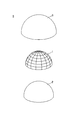
- FIG. 2 is an exploded perspective view illustrating the tactile sensor according to the first embodiment.
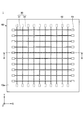
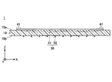
- FIG. 2 is a plan view illustrating a sensor main body of the tactile sensor according to the first embodiment. It is a sectional view (the 1) which illustrates the sensor main part of the tactile sensor concerning a 1st embodiment.
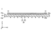
- FIG. 3 is a cross-sectional view (part 2) illustrating a sensor main body of the tactile sensor according to the first embodiment.
- FIG. 2 is a block diagram illustrating a tactile sensor module according to the first embodiment. It is a block diagram which illustrates the control device of the tactile sensor module concerning a 1st embodiment.
- FIG. 7 is a diagram (part 2) schematically showing a force transmitted to the sensor main body when the tactile sensor touches an object.
- FIG. 9 is a plan view illustrating a sensor body according to Modification Example 1 of the first embodiment.
- FIG. 1 is a perspective view illustrating the tactile sensor according to the first embodiment.
- FIG. 2 is an exploded perspective view illustrating the tactile sensor according to the first embodiment.
- the tactile sensor 5 includes a sensor main body 1, a support member 2, and a buffer member 3.
- the sensor main body 1 is disposed on the support member 2 and is covered with the cushioning member 3. That is, the sensor body 1 is sandwiched between the support member 2 and the buffer member 3. The sensor body 1 will be described later.
- the support member 2 is a member formed of metal, resin, or the like and having a curved surface.
- the shape of the support member 2 is not particularly limited as long as it is a member having a curved surface, and may be, for example, a hemisphere.
- the support member 2 may have a shape close to a human fingertip (a shape having a curved surface portion or a flat portion).
- the buffer member 3 is a member that covers the sensor main body 1 to mechanically protect the sensor main body 1 and that transmits a force received from the object to the sensor main body 1 when coming into contact with the object.
- the cushioning member 3 is preferably formed of an elastic body. Specific examples of the material include rubber such as silicone rubber and a polymer material such as polyurethane. Note that an elastic body refers to an object that is distorted when a force is applied, but returns to its original shape when the force is removed.
- FIG. 3 is a plan view illustrating the sensor main body of the tactile sensor according to the first embodiment, and shows a state before the sensor body is attached to the support member 2.
- FIG. 4 is a cross-sectional view illustrating the sensor main body of the tactile sensor according to the first embodiment, and shows a cross-section along line AA in FIG.
- the sensor main body 1 has a base material 10, a resistor 30 (a plurality of resistance portions 31 and 32), and a plurality of terminal portions 41 and 42.
- the planar shape of the sensor main body 1 is substantially square, but the sensor main body 1 can be appropriately processed into a planar shape that can be easily attached to the support member 2.
- the side on which the resistance portion 31 of the substrate 10 is provided is the upper side or one side, and the side on which the resistance portion 32 is provided is the lower side or the other side. Side.
- the surface on the side where the resistance portion 31 is provided is defined as one surface or upper surface, and the surface on the side where the resistance portion 32 is provided is defined as the other surface or lower surface.
- the sensor main body 1 can be used upside down, or can be arranged at an arbitrary angle.
- the plan view refers to viewing the target from the normal direction of the upper surface 10a of the base material 10
- the planar shape refers to the shape of the target viewed from the normal direction of the upper surface 10a of the base material 10.
- the base material 10 is an insulating member serving as a base layer for forming the resistor 30 and the like, and has flexibility.
- the thickness of the substrate 10 is not particularly limited and can be appropriately selected depending on the purpose. For example, the thickness can be about 5 ⁇ m to 500 ⁇ m. In particular, it is preferable that the thickness of the base material 10 be 5 ⁇ m to 200 ⁇ m, since the strain sensitivity error of the resistance portions 31 and 32 can be reduced.
- the substrate 10 is made of, for example, a PI (polyimide) resin, an epoxy resin, a PEEK (polyetheretherketone) resin, a PEN (polyethylene naphthalate) resin, a PET (polyethylene terephthalate) resin, a PPS (polyphenylene sulfide) resin, a polyolefin resin, or the like. From an insulating resin film.
- the film refers to a member having a thickness of about 500 ⁇ m or less and having flexibility.
- the base material 10 may be formed from, for example, an insulating resin film containing a filler such as silica or alumina.
- the base material 10 may be made of SiO 2 , ZrO 2 (including YSZ), Si, Si 2 N 3 , and Al 2 O 3 (including sapphire). , ZnO, perovskite ceramics (CaTiO 3 , BaTiO 3 ), and the like.
- the resistor 30 is formed on the base material 10 and is a sensing portion whose resistance value continuously changes according to the pressing force.
- the resistor 30 may be formed directly on the upper surface 10a and the lower surface 10b of the substrate 10, or may be formed on the upper surface 10a and the lower surface 10b of the substrate 10 via another layer.
- the resistor 30 includes a plurality of resistor portions 31 and 32 stacked with the base material 10 interposed therebetween. That is, the resistor 30 is a general term for the plurality of resistors 31 and 32, and is referred to as the resistor 30 unless it is necessary to particularly distinguish the resistors 31 and 32. In FIG. 3, for convenience, the resistance portions 31 and 32 are shown in a satin pattern.
- the plurality of resistance portions 31 are thin films that are juxtaposed in the Y direction at predetermined intervals on the upper surface 10a of the base material 10 with the longitudinal direction facing the X direction.
- the plurality of resistance portions 32 are thin films that are juxtaposed in the X direction at predetermined intervals on the lower surface 10b of the base material 10 with the longitudinal direction facing the Y direction.
- the plurality of resistance portions 31 and the plurality of resistance portions 32 do not need to be orthogonal to each other in a plan view, but may intersect.
- the resistor 30 can be formed from, for example, a material containing Cr (chromium), a material containing Ni (nickel), or a material containing both Cr and Ni. That is, the resistor 30 can be formed from a material containing at least one of Cr and Ni.
- a material containing Cr for example, a Cr mixed-phase film is given.
- the material containing Ni include, for example, Cu—Ni (copper nickel).
- Ni—Cr nickel chrome
- the Cr mixed phase film is a film in which Cr, CrN, Cr 2 N, and the like are mixed.
- the Cr mixed phase film may contain unavoidable impurities such as chromium oxide.
- the thickness of the resistor 30 is not particularly limited and can be appropriately selected depending on the purpose.
- the thickness can be about 0.05 ⁇ m to 2 ⁇ m.
- the thickness of the resistor 30 be 0.1 ⁇ m or more, since the crystallinity of the crystal constituting the resistor 30 (for example, the crystallinity of ⁇ -Cr) is improved.
- the thickness of the resistor 30 be 1 ⁇ m or less, since cracks in the film and warpage from the substrate 10 due to internal stress of the film constituting the resistor 30 can be reduced.
- the width of the resistor 30 is not particularly limited and can be appropriately selected depending on the purpose.
- the width can be about 0.1 ⁇ m to 1000 ⁇ m.
- the pitch between the adjacent resistors 30 is not particularly limited and can be appropriately selected according to the purpose.
- the pitch can be about 1 mm to 100 mm.
- FIG. 3 and FIG. 4 show ten resistance portions 31 and ten resistance portions 32, actually several hundred to several thousand resistance portions 31 and 32 are provided.
- the temperature coefficient of the resistor 30 can be stabilized by using ⁇ -Cr (alpha chromium), which is a stable crystal phase, as a main component, and the resistor 30 can withstand a pressing force.
- ⁇ -Cr alpha chromium
- the main component means that the target substance occupies 50% by mass or more of all the substances constituting the resistor.
- the main component stabilizes the temperature coefficient of the resistor 30 and the sensitivity of the resistor 30 to the pressing force.
- the resistor 30 preferably contains ⁇ -Cr in an amount of 80% by weight or more. Note that ⁇ -Cr is Cr having a bcc structure (body-centered cubic lattice structure).
- the terminal portions 41 extend from both ends of each of the resistance portions 31 on the upper surface 10a of the base material 10, and are formed in a substantially rectangular shape so as to be wider than the resistance portions 31 in plan view.
- the terminal portion 41 is a pair of electrodes for outputting a change in the resistance value of the resistance portion 31 caused by the pressing force to the outside.
- a flexible substrate or a lead wire for external connection is joined.
- the upper surface of the terminal portion 41 may be covered with a metal having better solderability than the terminal portion 41.
- the resistance part 31 and the terminal part 41 are shown with different symbols for convenience, they can be integrally formed of the same material in the same step.
- the terminal portions 42 extend from both ends of each of the resistor portions 32 on the lower surface 10b of the base material 10, and are formed in a substantially rectangular shape so as to be wider than the resistor portions 32 in a plan view.
- the terminal section 42 is a pair of electrodes for outputting a change in the resistance value of the resistance section 32 caused by the pressing force to the outside, and is connected to, for example, a flexible board or a lead wire for external connection.
- the upper surface of the terminal portion 42 may be covered with a metal having better solderability than the terminal portion 42.
- the resistance part 32 and the terminal part 42 are shown with different symbols for convenience, they can be integrally formed of the same material in the same step.
- a through wiring (through hole) penetrating the base material 10 may be provided, and the terminal portions 41 and 42 may be integrated on the upper surface 10a side or the lower surface 10b side of the base material 10.
- a cover layer may be provided on the upper surface 10a of the base material 10 so as to cover the resistance portion 31 and expose the terminal portion 41. Further, a cover layer (insulating resin layer) may be provided on the lower surface 10b of the base material 10 so as to cover the resistance portion 32 and expose the terminal portion 42.
- the cover layer By providing the cover layer, it is possible to prevent mechanical damage or the like from occurring in the resistance portions 31 and 32. By providing the cover layer, the resistance portions 31 and 32 can be protected from moisture and the like. Note that the cover layer may be provided so as to cover the entire portion except for the terminal portions 41 and 42.
- the cover layer can be formed from an insulating resin such as a PI resin, an epoxy resin, a PEEK resin, a PEN resin, a PET resin, a PPS resin, and a composite resin (for example, a silicone resin or a polyolefin resin).
- the cover layer may contain a filler or a pigment.
- the thickness of the cover layer is not particularly limited and can be appropriately selected depending on the purpose. For example, the thickness can be about 2 ⁇ m to 30 ⁇ m.
- the base material 10 is prepared, and the planar resistance part 31 and the terminal part 41 shown in FIG. 3 are formed on the upper surface 10 a of the base material 10.
- the materials and thicknesses of the resistance portion 31 and the terminal portion 41 are as described above.
- the resistance section 31 and the terminal section 41 can be integrally formed of the same material.
- the resistance portion 31 and the terminal portion 41 can be formed by, for example, forming a film by a magnetron sputtering method using a material capable of forming the resistance portion 31 and the terminal portion 41 as a target, and patterning the film by photolithography.
- the resistance section 31 and the terminal section 41 may be formed by a reactive sputtering method, an evaporation method, an arc ion plating method, a pulse laser deposition method, or the like instead of the magnetron sputtering method.
- the film thickness of the underlayer is 1 nm to 100 nm. It is preferable to form a functional layer with a degree of vacuum deposition.
- the functional layer can be formed, for example, by a conventional sputtering method. Note that, after forming the resistor portion 31 and the terminal portion 41 on the entire upper surface of the functional layer, the functional layer is patterned by photolithography together with the resistor portion 31 and the terminal portion 41 into the planar shape shown in FIG.
- the functional layer refers to a layer having a function of promoting crystal growth of at least the upper resistive portion.
- the functional layer preferably further has a function of preventing oxidation of the resistance portion by oxygen or moisture contained in the base material 10 and a function of improving adhesion between the base material 10 and the resistance portion.
- the functional layer may further have another function.
- the insulating resin film constituting the base material 10 contains oxygen and moisture, especially when the resistance portion contains Cr, Cr forms a self-oxidized film, so that the functional layer has a function of preventing oxidation of the resistance portion. Is valid.
- the material of the functional layer is not particularly limited and may be appropriately selected depending on the purpose as long as it has a function of promoting the crystal growth of at least the upper resistive portion.
- the material include Cr (chromium) and Ti (titanium). ), V (vanadium), Nb (niobium), Ta (tantalum), Ni (nickel), Y (yttrium), Zr (zirconium), Hf (hafnium), Si (silicon), C (carbon), Zn (zinc) ), Cu (copper), Bi (bismuth), Fe (iron), Mo (molybdenum), W (tungsten), Ru (ruthenium), Rh (rhodium), Re (rhenium), Os (osmium), Ir (iridium) ), Pt (platinum), Pd (palladium), Ag (silver), Au (gold), Co (cobalt), Mn (manganese), Al (aluminum) One or more metals, or metal alloys of this group, or
- Examples of the above alloy include FeCr, TiAl, FeNi, NiCr, CrCu and the like.
- Examples of the above compounds include TiN, TaN, Si 3 N 4 , TiO 2 , Ta 2 O 5 , and SiO 2 .
- the functional layer can be formed, for example, by a conventional sputtering method using a material capable of forming the functional layer as a target and introducing an Ar (argon) gas into the chamber.
- Ar argon
- the functional layer is formed while the upper surface 10a of the substrate 10 is etched with Ar, so that the effect of improving the adhesion can be obtained by minimizing the amount of the functional layer formed.
- the functional layer may be formed by another method.
- the upper surface 10a of the base material 10 is activated by plasma treatment using Ar or the like to obtain an adhesion improving effect, and thereafter, the functional layer is formed into a vacuum by a magnetron sputtering method. May be used.
- the combination of the material of the functional layer and the material of the resistor portion 31 and the terminal portion 41 is not particularly limited and can be appropriately selected depending on the purpose.
- the resistance section 31 and the terminal section 41 can be formed by a magnetron sputtering method using a raw material capable of forming a Cr mixed phase film as a target and introducing Ar gas into the chamber.
- the resistive portion 31 and the terminal portion 41 may be formed by reactive sputtering using a target of pure Cr and an appropriate amount of nitrogen gas together with Ar gas.
- the growth surface of the Cr mixed phase film is defined by the function layer made of Ti as a trigger, and a Cr mixed phase film having ⁇ -Cr as a main component, which has a stable crystal structure, can be formed. Further, by diffusing Ti constituting the functional layer into the Cr mixed phase film, it is possible to stabilize the temperature coefficient of the resistance portion 31 and to improve the sensitivity of the resistance portion 31 to the pressing force.
- the Cr mixed phase film may include Ti or TiN (titanium nitride).
- the functional layer made of Ti has a function of promoting crystal growth of the resistance part 31 and a function of preventing oxidation of the resistance part 31 by oxygen or moisture contained in the base material 10. And all the functions of improving the adhesion between the base material 10 and the resistance portion 31.
- Ta, Si, Al, or Fe is used instead of Ti as the functional layer.
- the crystal growth of the resistor 31 can be promoted, and the resistor 31 having a stable crystal phase can be manufactured.
- the temperature coefficient of the resistance portion 31 can be stabilized, and the sensitivity of the resistance portion 31 to the pressing force can be improved.
- the material forming the functional layer diffuses into the resistance portion 31, the temperature coefficient of the resistance portion 31 can be stabilized and the sensitivity of the resistance portion 31 to the pressing force can be improved in the sensor body 1. .
- the planar resistive portion 32 and the terminal portion 42 shown in FIG. 3 are formed on the lower surface 10b of the base material 10.
- the resistance part 32 and the terminal part 42 can be formed in the same manner as the resistance part 31 and the terminal part 41.
- a cover layer that covers the resistance part 31 on the upper surface 10 a of the base material 10 and exposes the terminal part 41 may be formed on the base material 10.
- a cover layer that covers the resistance portion 32 and exposes the terminal portion 42 may be provided on the lower surface 10b.
- the cover layer is formed, for example, by laminating a thermosetting insulating resin film in a semi-cured state so as to cover the resistance portion 31 on the upper surface 10a of the base material 10 and expose the terminal portion 41, and then heat and cure the film. be able to.
- the cover layer may be formed, for example, by laminating a thermosetting insulating resin film in a semi-cured state so as to cover the resistance portion 32 on the lower surface 10b of the base material 10 and expose the terminal portion 42, and then cure by heating. Can be made.
- the cover layer may be formed by applying a liquid or paste-like thermosetting insulating resin and heating and curing the resin.
- the sensor body 1 has the cross-sectional shape shown in FIG. Layers indicated by reference numerals 20a and 20b are functional layers.
- the planar shape of the sensor main body 1 when the functional layers 20a and 20b are provided is the same as that in FIG.
- the tactile sensor module 8 can be realized by the tactile sensor 5 and the control device 7.
- the tactile sensor 5 is attached to, for example, a fingertip of a robot hand, and the control device 7 can detect a contact point with the object when the robot grips the object, a gripping force, and the like.
- a plurality of tactile sensors 5 may be attached to a plurality of fingertips of the robot hand.
- the tactile sensor 5 is attached to each of the two fingertips of the robot hand, and when the object is gripped by the two fingertips of the robot hand, the robot is controlled by the control device 7 based on the output of each tactile sensor 5. It is possible to detect a contact position, a grip force, and the like with the object when the object is gripped.
- the terminals 41 and 42 of the sensor main body 1 in the tactile sensor 5 are connected to the control device 7 using, for example, a flexible substrate or a lead wire.
- the control device 7 can detect the coordinates of the position where the sensor main body 1 of the tactile sensor 5 is pressed and the magnitude of the pressing force based on the information obtained via the terminal portions 41 and 42 of the sensor main body 1. it can.
- the resistance part 31 of the sensor main body 1 can be used for detecting the X coordinate
- the resistance part 32 can be used for detecting the Y coordinate.
- control device 7 can be configured to include, for example, an analog front-end unit 71 and a signal processing unit 72.
- the analog front end unit 71 includes, for example, an input signal selection switch, a bridge circuit, an amplifier, an analog / digital conversion circuit (A / D conversion circuit), and the like.
- the analog front end unit 71 may include a temperature compensation circuit.
- all the terminal units 41 and 42 of the sensor body 1 are connected to the input signal selection switch, and a pair of electrodes is selected by the input signal selection switch.
- the pair of electrodes selected by the input signal selection switch is connected to a bridge circuit.
- one side of the bridge circuit is formed of a resistor between a pair of electrodes selected by the input signal selection switch, and the other three sides are formed of fixed resistors.
- a voltage (analog signal) corresponding to the resistance value of the resistor between the pair of electrodes selected by the input signal selection switch can be obtained as the output of the bridge circuit.
- the input signal selection switch is configured to be controllable by the signal processing unit 72.
- the voltage output from the bridge circuit is amplified by an amplifier, converted to a digital signal by an A / D conversion circuit, and sent to the signal processing unit 72.
- the analog front end unit 71 has a temperature compensation circuit, a digital signal whose temperature has been compensated is sent to the signal processing unit 72.
- a digital signal corresponding to the resistance values of all the terminals 41 and 42 of the sensor main body 1 can be sent to the signal processing unit 72 in a very short time.
- the signal processing unit 72 can detect the coordinates of the position where the sensor body 1 is pressed and the magnitude of the pressing force based on the information sent from the analog front end unit 71.
- the magnitude of the pressing force is small, for example, only the resistance portion closer to the pressed side of the resistance portions 31 and 32 is pressed, and the resistance portion farther from the pressed side is It may not be pressed. In this case, only the resistance value between a pair of electrodes of the resistance portion closer to the pressed side changes continuously according to the magnitude of the pressing force, but also in this case, the signal processing unit 72 The magnitude of the pressing force can be detected based on the magnitude of the change in the resistance value of the resistance portion closer to the pressed side.
- the resistance value between the pair of electrodes of the pressed resistance part depends on the magnitude of the pressing force. Change continuously.
- the signal processing unit 72 determines the magnitude of the pressing force based on the magnitude of the change in the resistance value of the pressed resistance unit regardless of whether one of the resistance unit 31 and the resistance unit 32 is pressed or both. Can be detected.
- the signal processing unit 72 can be configured to include, for example, a CPU (Central Processing Unit), a ROM (Read Only Memory), a RAM (Random Access Memory), a main memory, and the like.
- a CPU Central Processing Unit
- ROM Read Only Memory
- RAM Random Access Memory
- various functions of the signal processing unit 72 can be realized by reading a program recorded in a ROM or the like into the main memory and executing the program by the CPU.
- part or all of the signal processing unit 72 may be realized only by hardware.
- the signal processing unit 72 may be physically configured by a plurality of devices or the like.
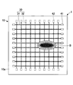
- FIGS. 8A and 8B are diagrams schematically showing a force transmitted to the sensor main body when the tactile sensor touches an object.
- FIG. 8A is a perspective view
- FIG. 8B is a plan view schematically showing how the sensor body detects a force.
- the cushioning member 3 when the tactile sensor 5 touches the object 300, the cushioning member 3 is deformed and the force is transmitted to the sensor main body 1.
- the force can be detected not as point data but as surface data in the sensor body 1, as shown in part B of FIG. 8B. This makes it possible to detect at which position of the fingertip and with what force the object is gripped.
- the part B the state that the force increases as the position is closer to the center and decreases as the position approaches the periphery is schematically illustrated by different satin patterns.
- the tactile sensor 5 When the tactile sensor 5 is attached to each of a plurality of fingertips of the robot hand and the object is gripped by the plurality of fingertips of the robot hand, the center of gravity of the object gripped by the robot is detected based on the output of each tactile sensor 5. it can.
- the tactile sensor 5 when the buffer member 3 comes into contact with the object, the buffer member 3 is deformed and the force received from the object is transmitted to the sensor main body 1, and the resistance portions 31 and 32 are pressed.
- the resistance portions 31 and 32 of the sensor body 1 are pressed, the pressed resistance portions 31 and 32 bend according to the pressing force, and the resistance value between the pair of electrodes of the pressed resistance portions 31 and 32 is reduced. It changes continuously according to the magnitude of the pressure. That is, the tactile sensor 5 can obtain three-dimensional information (the coordinates of the pressed position and the magnitude of the pressing force).
- the three-dimensional information obtained by the sensor main body 1 is sent to the control device 7, and the control device 7 determines the position where the sensor main body 1 is pressed based on the three-dimensional information obtained by the sensor main body 1. And the magnitude of the pressing force.
- the sensitivity of the resistance value to the force (the same as when the resistance parts 31 and 32 are formed from Cu—Ni or Ni—Cr).
- the amount of change in the resistance value of the resistance portions 31 and 32 with respect to the pressing force) is greatly improved.
- the resistance portions 31 and 32 are formed of the Cr mixed phase film
- the sensitivity of the resistance value to the force is about 5 to 10 times as compared with the case where the resistance portions 31 and 32 are formed of Cu—Ni or Ni—Cr. About double. Therefore, by forming the resistance portions 31 and 32 from a Cr mixed phase film, the detection accuracy of the coordinates of the pressed position can be improved, and the force can be detected with high sensitivity.
- a predetermined operation is performed when it is detected that the force is small, and another operation is performed when it is detected that the force is medium. Is large, it is possible to realize control for performing another operation. Alternatively, it is possible to realize a control in which the operation is not performed when it is detected that the force is small or medium, and the predetermined operation is performed only when it is detected that the force is large.
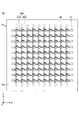
- FIG. 9 is a plan view illustrating a sensor body according to Modification 1 of the first embodiment, and shows a plane corresponding to FIG.
- the sensor main body 1A differs from the sensor main body 1 (see FIGS. 3 and 4) in that the resistor 30 is replaced with a resistor 30A.
- the resistor 30A includes the resistor portions 31A and 32A.
- the resistance portion 31A is a zigzag pattern formed between the pair of terminal portions 41.
- the resistor 32A is a zigzag pattern formed between the pair of terminals 42.
- the material and thickness of the resistance portions 31A and 32A can be the same as the material and thickness of the resistance portions 31 and 32, for example.
- the resistance value between the pair of terminal portions 41 and the resistance value between the pair of terminal portions 42 are reduced as compared with the case of forming a linear pattern. Can be higher.
- the amount of change in the resistance value between the pair of terminal portions 41 and the amount of change in the resistance value between the pair of terminal portions 42 when pressed are increased, so that the detection accuracy of the coordinates of the pressed position is improved.
- the force can be further improved and the force can be detected with higher sensitivity.
- the resistance between the pair of terminals 41 and the resistance between the pair of terminals 42 can be increased, the power consumption of the sensor body 1A can be reduced.
- the resistance portion 31 is provided on the upper surface 10a of the base material 10 as the insulating layer and the resistance portion 32 is provided on the lower surface 10b has been described, but the resistance portion 32 is provided on one side of the insulating layer.
- the present invention is not limited to this, as long as the resistor portion 32 is provided on the other side.
- the resistance part 31 may be provided on the upper surface 10a of the base material 10
- the insulating layer covering the resistance part 31 may be provided on the upper surface 10a of the base material 10
- the resistance part 32 may be provided on the insulating layer.
- a first base material provided with the resistance part 31 and a second base material provided with the resistance part 32 are manufactured, and the resistance part 31 and the resistance part 32 are directed inward, and the resistance part 31 is sandwiched with an insulating layer therebetween.
- the provided first base material and the second base material provided with the resistance portion 32 may be bonded together.
- a first base material provided with the resistance part 31 and a second base material provided with the resistance part 32 are produced, and the first base material provided with the resistance part 31 and the second base material provided with the resistance part 32 are prepared. They may be stacked in the same direction. The same applies to the sensor body 1A.
Landscapes
- Engineering & Computer Science (AREA)
- Physics & Mathematics (AREA)
- General Physics & Mathematics (AREA)
- Human Computer Interaction (AREA)
- Robotics (AREA)
- Mechanical Engineering (AREA)
- Chemical & Material Sciences (AREA)
- Analytical Chemistry (AREA)
- Force Measurement Appropriate To Specific Purposes (AREA)
Abstract
本触覚センサは、曲面を有する支持部材と、前記支持部材上に配置されたセンサ本体と、前記センサ本体を被覆し、物体に接すると前記物体から受けた力を前記センサ本体に伝達する緩衝部材と、を備え、前記センサ本体は、絶縁層と、前記絶縁層の一方の側に長手方向を第1方向に向けて並置された複数の第1抵抗部と、前記絶縁層の他方の側に長手方向を前記第1方向と交差する第2方向に向けて並置された複数の第2抵抗部と、各々の前記第1抵抗部及び各々の前記第2抵抗部の両端部に設けられた1対の電極と、を有し、前記物体から受けた力が前記センサ本体に伝達され、前記第1抵抗部及び/又は前記第2抵抗部が押圧されると、押圧された前記第1抵抗部及び/又は前記第2抵抗部の前記1対の電極間の抵抗値が押圧力の大きさに応じて連続的に変化する。
Description
本発明は、触覚センサに関する。
近年、ロボットハンド等に用いる触覚センサの研究開発が行われており、様々な方式の触覚センサが知られている。
例えば、プリント基板の端面からみて、プリント基板の一方の面に、所定方向(X軸方向)に所定ピッチで金属箔が形成され、他方の面に金属箔が全面に貼着されたプリント基板を、その厚さ方向(Y軸方向)に絶縁材を挟んで複数積層した触覚センサが挙げられる。
この触覚センサでは、積層されたプリント基板の端面に導電性シートを被着している。そして、導電性シートの一部を加圧すると、加圧された部分のX軸に位置する金属箔部分とY軸に位置する金属箔部分とが導電性シートを介して導通することにより、加圧部分の位置を電気的に検出できる(例えば、特許文献1参照)。
しかしながら、上記の触覚センサでは、XY方向の2次元情報は得られるものの、Z方向も含めた3次元情報を得ることはできなかった。
本発明は、上記の点に鑑みてなされたもので、3次元情報が得られる触覚センサを提供することを目的とする。
本触覚センサは、曲面を有する支持部材と、前記支持部材上に配置されたセンサ本体と、前記センサ本体を被覆し、物体に接すると前記物体から受けた力を前記センサ本体に伝達する緩衝部材と、を備え、前記センサ本体は、絶縁層と、前記絶縁層の一方の側に長手方向を第1方向に向けて並置された複数の第1抵抗部と、前記絶縁層の他方の側に長手方向を前記第1方向と交差する第2方向に向けて並置された複数の第2抵抗部と、各々の前記第1抵抗部及び各々の前記第2抵抗部の両端部に設けられた1対の電極と、を有し、前記物体から受けた力が前記センサ本体に伝達され、前記第1抵抗部及び/又は前記第2抵抗部が押圧されると、押圧された前記第1抵抗部及び/又は前記第2抵抗部の前記1対の電極間の抵抗値が押圧力の大きさに応じて連続的に変化する。
開示の技術によれば、3次元情報が得られる触覚センサを提供できる。
以下、図面を参照して発明を実施するための形態について説明する。各図面において、同一構成部分には同一符号を付し、重複した説明を省略する場合がある。
〈第1の実施の形態〉
図1は、第1の実施の形態に係る触覚センサを例示する斜視図である。図2は、第1の実施の形態に係る触覚センサを例示する分解斜視図である。図1及び図2を参照するに、触覚センサ5は、センサ本体1と、支持部材2と、緩衝部材3とを有している。
図1は、第1の実施の形態に係る触覚センサを例示する斜視図である。図2は、第1の実施の形態に係る触覚センサを例示する分解斜視図である。図1及び図2を参照するに、触覚センサ5は、センサ本体1と、支持部材2と、緩衝部材3とを有している。
触覚センサ5において、センサ本体1は、支持部材2上に配置され、緩衝部材3により被覆されている。つまり、センサ本体1は、支持部材2と緩衝部材3に挟持されている。センサ本体1については後述する。
支持部材2は、金属や樹脂等から形成された、曲面を有する部材である。支持部材2の形状は、曲面を有する部材であれば特に限定されないが、例えば半球状とすることができる。支持部材2を人間の指先に近い形状(曲面部や偏平部を有する形状)としてもよい。
緩衝部材3は、センサ本体1を被覆して機械的に保護すると共に、物体に接すると物体から受けた力をセンサ本体1に伝達する部材である。緩衝部材3は、弾性体から形成することが好ましく、具体的な材料としては、例えば、シリコーンゴム等のゴムや、ポリウレタン等の高分子材料が挙げられる。なお、弾性体とは、力を加えるとひずみが生じるが、力を除去すれば元の形状に戻る物体を指す。
図3は、第1の実施の形態に係る触覚センサのセンサ本体を例示する平面図であり、支持部材2に貼り付ける前の状態を示している。図4は、第1の実施の形態に係る触覚センサのセンサ本体を例示する断面図であり、図3のA-A線に沿う断面を示している。
図3及び図4を参照するに、センサ本体1は、基材10と、抵抗体30(複数の抵抗部31及び32)と、複数の端子部41及び42とを有している。図3では、便宜上、センサ本体1の平面形状を略正方形としているが、センサ本体1は支持部材2に貼り付けやすいような平面形状に適宜加工することができる。
なお、本実施の形態では、便宜上、センサ本体1において、基材10の抵抗部31が設けられている側を上側又は一方の側、抵抗部32が設けられている側を下側又は他方の側とする。又、各部位の抵抗部31が設けられている側の面を一方の面又は上面、抵抗部32が設けられている側の面を他方の面又は下面とする。但し、センサ本体1は天地逆の状態で用いることができ、又は任意の角度で配置することができる。又、平面視とは対象物を基材10の上面10aの法線方向から視ることを指し、平面形状とは対象物を基材10の上面10aの法線方向から視た形状を指すものとする。
基材10は、抵抗体30等を形成するためのベース層となる絶縁性の部材であり、可撓性を有する。基材10の厚さは、特に制限はなく、目的に応じて適宜選択できるが、例えば、5μm~500μm程度とすることができる。特に、基材10の厚さが5μm~200μmであると、抵抗部31及び32のひずみ感度誤差を少なくすることができる点で好ましい。
基材10は、例えば、PI(ポリイミド)樹脂、エポキシ樹脂、PEEK(ポリエーテルエーテルケトン)樹脂、PEN(ポリエチレンナフタレート)樹脂、PET(ポリエチレンテレフタレート)樹脂、PPS(ポリフェニレンサルファイド)樹脂、ポリオレフィン樹脂等の絶縁樹脂フィルムから形成することができる。なお、フィルムとは、厚さが500μm以下程度であり、可撓性を有する部材を指す。
ここで、『絶縁樹脂フィルムから形成する』とは、基材10が絶縁樹脂フィルム中にフィラーや不純物等を含有することを妨げるものではない。基材10は、例えば、シリカやアルミナ等のフィラーを含有する絶縁樹脂フィルムから形成しても構わない。
但し、基材10が可撓性を有する必要がない場合には、基材10に、SiO2、ZrO2(YSZも含む)、Si、Si2N3、Al2O3(サファイヤも含む)、ZnO、ペロブスカイト系セラミックス(CaTiO3、BaTiO3)等の材料を用いても構わない。
抵抗体30は、基材10上に形成されており、押圧力に応じて連続的に抵抗値が変化する受感部である。抵抗体30は、基材10の上面10a及び下面10bに直接形成されてもよいし、基材10の上面10a及び下面10bに他の層を介して形成されてもよい。
抵抗体30は、基材10を介して積層された複数の抵抗部31及び32を含んでいる。すなわち、抵抗体30は、複数の抵抗部31及び32の総称であり、抵抗部31及び32を特に区別する必要がない場合には抵抗体30と称する。なお、図3では、便宜上、抵抗部31及び32を梨地模様で示している。
複数の抵抗部31は、基材10の上面10aに、長手方向をX方向に向けて所定間隔でY方向に並置された薄膜である。複数の抵抗部32は、基材10の下面10bに、長手方向をY方向に向けて所定間隔でX方向に並置された薄膜である。但し、複数の抵抗部31と複数の抵抗部32とは平面視で直交している必要はなく、交差していればよい。
抵抗体30は、例えば、Cr(クロム)を含む材料、Ni(ニッケル)を含む材料、又はCrとNiの両方を含む材料から形成することができる。すなわち、抵抗体30は、CrとNiの少なくとも一方を含む材料から形成することができる。Crを含む材料としては、例えば、Cr混相膜が挙げられる。Niを含む材料としては、例えば、Cu-Ni(銅ニッケル)が挙げられる。CrとNiの両方を含む材料としては、例えば、Ni-Cr(ニッケルクロム)が挙げられる。
ここで、Cr混相膜とは、Cr、CrN、Cr2N等が混相した膜である。Cr混相膜は、酸化クロム等の不可避不純物を含んでもよい。
抵抗体30の厚さは、特に制限はなく、目的に応じて適宜選択できるが、例えば、0.05μm~2μm程度とすることができる。特に、抵抗体30の厚さが0.1μm以上であると、抵抗体30を構成する結晶の結晶性(例えば、α-Crの結晶性)が向上する点で好ましい。又、抵抗体30の厚さが1μm以下であると、抵抗体30を構成する膜の内部応力に起因する膜のクラックや基材10からの反りを低減できる点で更に好ましい。
抵抗体30の幅は、特に制限はなく、目的に応じて適宜選択できるが、例えば、0.1μm~1000μm程度とすることができる。隣接する抵抗体30のピッチは、特に制限はなく、目的に応じて適宜選択できるが、例えば、1mm~100mm程度とすることができる。なお、図3及び図4では、抵抗部31を10本、抵抗部32を10本図示しているが、抵抗部31及び32は、実際には数100~数1000本程度設けられる。
例えば、抵抗体30がCr混相膜である場合、安定な結晶相であるα-Cr(アルファクロム)を主成分とすることで、抵抗体30の温度係数の安定化や、押圧力に対する抵抗体30の感度の向上を実現できる。ここで、主成分とは、対象物質が抵抗体を構成する全物質の50質量%以上を占めることを意味するが、抵抗体30の温度係数の安定化や、押圧力に対する抵抗体30の感度の向上を実現する観点から、抵抗体30はα-Crを80重量%以上含むことが好ましい。なお、α-Crは、bcc構造(体心立方格子構造)のCrである。
端子部41は、基材10の上面10aにおいて、各々の抵抗部31の両端部から延在しており、平面視において、抵抗部31よりも拡幅して略矩形状に形成されている。端子部41は、押圧力により生じる抵抗部31の抵抗値の変化を外部に出力するための1対の電極であり、例えば、外部接続用のフレキシブル基板やリード線等が接合される。端子部41の上面を、端子部41よりもはんだ付け性が良好な金属で被覆してもよい。なお、抵抗部31と端子部41とは便宜上別符号としているが、両者は同一工程において同一材料により一体に形成することができる。
端子部42は、基材10の下面10bにおいて、各々の抵抗部32の両端部から延在しており、平面視において、抵抗部32よりも拡幅して略矩形状に形成されている。端子部42は、押圧力により生じる抵抗部32の抵抗値の変化を外部に出力するための1対の電極であり、例えば、外部接続用のフレキシブル基板やリード線等が接合される。端子部42の上面を、端子部42よりもはんだ付け性が良好な金属で被覆してもよい。なお、抵抗部32と端子部42とは便宜上別符号としているが、両者は同一工程において同一材料により一体に形成することができる。
なお、基材10を貫通する貫通配線(スルーホール)を設け、端子部41及び42を基材10の上面10a側又は下面10b側に集約してもよい。
抵抗部31を被覆し端子部41を露出するように基材10の上面10aにカバー層(絶縁樹脂層)を設けても構わない。又、抵抗部32を被覆し端子部42を露出するように基材10の下面10bにカバー層(絶縁樹脂層)を設けても構わない。カバー層を設けることで、抵抗部31及び32に機械的な損傷等が生じることを防止できる。又、カバー層を設けることで、抵抗部31及び32を湿気等から保護することができる。なお、カバー層は、端子部41及び42を除く部分の全体を覆うように設けてもよい。
カバー層は、例えば、PI樹脂、エポキシ樹脂、PEEK樹脂、PEN樹脂、PET樹脂、PPS樹脂、複合樹脂(例えば、シリコーン樹脂、ポリオレフィン樹脂)等の絶縁樹脂から形成することができる。カバー層は、フィラーや顔料を含有しても構わない。カバー層の厚さは、特に制限はなく、目的に応じて適宜選択できるが、例えば、2μm~30μm程度とすることができる。
センサ本体1を製造するためには、まず、基材10を準備し、基材10の上面10aに図3に示す平面形状の抵抗部31及び端子部41を形成する。抵抗部31及び端子部41の材料や厚さは、前述の通りである。抵抗部31と端子部41とは、同一材料により一体に形成することができる。
抵抗部31及び端子部41は、例えば、抵抗部31及び端子部41を形成可能な原料をターゲットとしたマグネトロンスパッタ法により成膜し、フォトリソグラフィによってパターニングすることで形成できる。抵抗部31及び端子部41は、マグネトロンスパッタ法に代えて、反応性スパッタ法や蒸着法、アークイオンプレーティング法、パルスレーザー堆積法等を用いて成膜してもよい。
抵抗部31の温度係数の安定化や、押圧力に対する抵抗部31の感度の向上を実現する観点から、抵抗部31及び端子部41を成膜する前に、下地層として膜厚が1nm~100nm程度の機能層を真空成膜することが好ましい。機能層は、例えば、コンベンショナルスパッタ法により成膜できる。なお、機能層は、機能層の上面全体に抵抗部31及び端子部41を形成後、フォトリソグラフィによって抵抗部31及び端子部41と共に図3に示す平面形状にパターニングされる。
本願において、機能層とは、少なくとも上層である抵抗部の結晶成長を促進する機能を有する層を指す。機能層は、更に、基材10に含まれる酸素や水分による抵抗部の酸化を防止する機能や、基材10と抵抗部との密着性を向上する機能を備えていることが好ましい。機能層は、更に、他の機能を備えていてもよい。
基材10を構成する絶縁樹脂フィルムは酸素や水分を含むため、特に抵抗部がCrを含む場合、Crは自己酸化膜を形成するため、機能層が抵抗部の酸化を防止する機能を備えることは有効である。
機能層の材料は、少なくとも上層である抵抗部の結晶成長を促進する機能を有する材料であれば、特に制限はなく、目的に応じて適宜選択できるが、例えば、Cr(クロム)、Ti(チタン)、V(バナジウム)、Nb(ニオブ)、Ta(タンタル)、Ni(ニッケル)、Y(イットリウム)、Zr(ジルコニウム)、Hf(ハフニウム)、Si(シリコン)、C(炭素)、Zn(亜鉛)、Cu(銅)、Bi(ビスマス)、Fe(鉄)、Mo(モリブデン)、W(タングステン)、Ru(ルテニウム)、Rh(ロジウム)、Re(レニウム)、Os(オスミウム)、Ir(イリジウム)、Pt(白金)、Pd(パラジウム)、Ag(銀)、Au(金)、Co(コバルト)、Mn(マンガン)、Al(アルミニウム)からなる群から選択される1種又は複数種の金属、この群の何れかの金属の合金、又は、この群の何れかの金属の化合物が挙げられる。
上記の合金としては、例えば、FeCr、TiAl、FeNi、NiCr、CrCu等が挙げられる。又、上記の化合物としては、例えば、TiN、TaN、Si3N4、TiO2、Ta2O5、SiO2等が挙げられる。
機能層は、例えば、機能層を形成可能な原料をターゲットとし、チャンバ内にAr(アルゴン)ガスを導入したコンベンショナルスパッタ法により真空成膜することができる。コンベンショナルスパッタ法を用いることにより、基材10の上面10aをArでエッチングしながら機能層が成膜されるため、機能層の成膜量を最小限にして密着性改善効果を得ることができる。
但し、これは、機能層の成膜方法の一例であり、他の方法により機能層を成膜してもよい。例えば、機能層の成膜の前にAr等を用いたプラズマ処理等により基材10の上面10aを活性化することで密着性改善効果を獲得し、その後マグネトロンスパッタ法により機能層を真空成膜する方法を用いてもよい。
機能層の材料と抵抗部31及び端子部41の材料との組み合わせは、特に制限はなく、目的に応じて適宜選択できる。例えば、機能層としてTiを用い、抵抗部31及び端子部41としてα-Cr(アルファクロム)を主成分とするCr混相膜を成膜することが可能である。
この場合、例えば、Cr混相膜を形成可能な原料をターゲットとし、チャンバ内にArガスを導入したマグネトロンスパッタ法により、抵抗部31及び端子部41を成膜することができる。或いは、純Crをターゲットとし、チャンバ内にArガスと共に適量の窒素ガスを導入し、反応性スパッタ法により、抵抗部31及び端子部41を成膜してもよい。
これらの方法では、Tiからなる機能層がきっかけでCr混相膜の成長面が規定され、安定な結晶構造であるα-Crを主成分とするCr混相膜を成膜できる。又、機能層を構成するTiがCr混相膜中に拡散することにより、抵抗部31の温度係数の安定化や、押圧力に対する抵抗部31の感度の向上を実現できる。なお、機能層がTiから形成されている場合、Cr混相膜にTiやTiN(窒化チタン)が含まれる場合がある。
なお、抵抗部31がCr混相膜である場合、Tiからなる機能層は、抵抗部31の結晶成長を促進する機能、基材10に含まれる酸素や水分による抵抗部31の酸化を防止する機能、及び基材10と抵抗部31との密着性を向上する機能の全てを備えている。機能層として、Tiに代えてTa、Si、Al、Feを用いた場合も同様である。
このように、抵抗部31の下層に機能層を設けることにより、抵抗部31の結晶成長を促進することが可能となり、安定な結晶相からなる抵抗部31を作製できる。その結果、センサ本体1において、抵抗部31の温度係数の安定化や、押圧力に対する抵抗部31の感度の向上を実現することができる。又、機能層を構成する材料が抵抗部31に拡散することにより、センサ本体1において、抵抗部31の温度係数の安定化や、押圧力に対する抵抗部31の感度の向上を実現することができる。
次に、基材10の下面10bに図3に示す平面形状の抵抗部32及び端子部42を形成する。抵抗部32及び端子部42は、抵抗部31及び端子部41と同様の方法で形成することができる。抵抗部32及び端子部42を成膜する前に、下地層として、基材10の下面10bに機能層を成膜することが好ましい点も同様である。
抵抗部31及び端子部41並びに抵抗部32及び端子部42を形成後、必要に応じ、基材10の上面10aに抵抗部31を被覆し端子部41を露出するカバー層を、基材10の下面10bに抵抗部32を被覆し端子部42を露出するカバー層を設けてもよい。これにより、センサ本体1が完成する。
カバー層は、例えば、基材10の上面10aに抵抗部31を被覆し端子部41を露出するように半硬化状態の熱硬化性の絶縁樹脂フィルムをラミネートし、加熱して硬化させて作製することができる。又、カバー層は、例えば、基材10の下面10bに抵抗部32を被覆し端子部42を露出するように半硬化状態の熱硬化性の絶縁樹脂フィルムをラミネートし、加熱して硬化させて作製することができる。カバー層は、絶縁樹脂フィルムのラミネートに代えて、液状又はペースト状の熱硬化性の絶縁樹脂を塗布し、加熱して硬化させて作製してもよい。
なお、抵抗部31及び端子部41の下地層として基材10の上面10aに機能層を設け、抵抗部32及び端子部42の下地層として基材10の下面10bに機能層を設けた場合には、センサ本体1は図5に示す断面形状となる。符号20a及び20bで示す層が機能層である。機能層20a及び20bを設けた場合のセンサ本体1の平面形状は、図3と同様である。
図6に示すように、触覚センサ5及び制御装置7により触覚センサモジュール8を実現できる。触覚センサモジュール8において、触覚センサ5は、例えば、ロボットハンドの指先に取り付けられ、制御装置7によりロボットが物体を把持した際の物体との接触個所や把持力等を検出することができる。複数の触覚センサ5をロボットハンドの複数の指先に取り付けてもよい。例えば、ロボットハンドの2本の指先の各々に触覚センサ5を取り付け、ロボットハンドの2本の指先で物体を把持した際に、各々の触覚センサ5の出力に基づいて、制御装置7によりロボットが対象物を把持した際の物体との接触位置や把持力等を検出できる。
触覚センサモジュール8において、触覚センサ5におけるセンサ本体1の各々の端子部41及び42は、例えば、フレキシブル基板やリード線等を用いて、制御装置7に接続されている。
制御装置7は、センサ本体1の端子部41及び42を介して得られた情報に基づいて、触覚センサ5のセンサ本体1が押圧された位置の座標や押圧力の大きさを検出することができる。例えば、センサ本体1の抵抗部31はX座標の検出に用いることができ、抵抗部32はY座標の検出に用いることができる。
図7に示すように、制御装置7は、例えば、アナログフロントエンド部71と、信号処理部72とを含む構成とすることができる。
アナログフロントエンド部71は、例えば、入力信号選択スイッチ、ブリッジ回路、増幅器、アナログ/デジタル変換回路(A/D変換回路)等を備えている。アナログフロントエンド部71は、温度補償回路を備えていてもよい。
アナログフロントエンド部71では、例えば、センサ本体1の全ての端子部41及び42が入力信号選択スイッチに接続され、入力信号選択スイッチにより1対の電極が選択される。入力信号選択スイッチで選択された1対の電極は、ブリッジ回路に接続される。
すなわち、ブリッジ回路の1辺が入力信号選択スイッチで選択された1対の電極間の抵抗部で構成され、他の3辺が固定抵抗で構成される。これにより、ブリッジ回路の出力として、入力信号選択スイッチで選択された1対の電極間の抵抗部の抵抗値に対応した電圧(アナログ信号)を得ることができる。なお、入力信号選択スイッチは、信号処理部72から制御可能に構成されている。
ブリッジ回路から出力された電圧は、増幅器で増幅された後、A/D変換回路によりデジタル信号に変換され、信号処理部72に送られる。アナログフロントエンド部71が温度補償回路を備えている場合には、温度補償されたデジタル信号が信号処理部72に送られる。入力信号選択スイッチを高速で切り替えることで、センサ本体1の全ての端子部41及び42の抵抗値に対応するデジタル信号を極短時間で信号処理部72に送ることができる。
信号処理部72は、アナログフロントエンド部71から送られた情報に基づいて、センサ本体1が押圧された位置の座標や押圧力の大きさを検出することができる。
又、複数の抵抗部31の抵抗値や複数の抵抗部32の抵抗値が変化した場合には、センサ本体1が複数位置で押圧されたことを検出できる。
なお、押圧力の大きさが小さい場合等には、抵抗部31及び抵抗部32のうち、押圧される側に近い方の抵抗部のみが押圧され、押圧される側から遠い方の抵抗部は押圧されない場合がある。この場合には、押圧される側に近い方の抵抗部の1対の電極間の抵抗値のみが押圧力の大きさに応じて連続的に変化するが、この場合も、信号処理部72は、押圧される側に近い方の抵抗部の抵抗値の変化の大小に基づいて、押圧力の大きさを検出することができる。
つまり、抵抗部31及び/又は抵抗部32が押圧されると、押圧された抵抗部(抵抗部31及び/又は抵抗部32)の1対の電極間の抵抗値が押圧力の大きさに応じて連続的に変化する。そして、信号処理部72は、抵抗部31と抵抗部32の一方が押圧されたか両方が押圧されたかにかかわらず、押圧された抵抗部の抵抗値の変化の大小に基づいて、押圧力の大きさを検出することができる。
信号処理部72は、例えば、CPU(Central Processing Unit)、ROM(Read Only Memory)、RAM(Random Access Memory)、メインメモリ等を含む構成とすることができる。
この場合、信号処理部72の各種機能は、ROM等に記録されたプログラムがメインメモリに読み出されてCPUにより実行されることによって実現できる。但し、信号処理部72の一部又は全部は、ハードウェアのみにより実現されてもよい。又、信号処理部72は、物理的に複数の装置等により構成されてもよい。
図8A及び図8Bは、触覚センサが物体に触れたときにセンサ本体に伝達される力を模式的に示す図である。図8Aは斜視図であり、図8Bはセンサ本体が力を検出する様子を平面図で模式的に示したものである。
図8Aに示すように、触覚センサ5が物体300に触れると、緩衝部材3が変形してセンサ本体1に力が伝達される。緩衝部材3が変形することで、図8BのB部に示すように、センサ本体1において、力を点データではなく面データとして検出できる。これにより、指先のどの位置で、どの程度の力で物体を把持しているかを検出できる。なお、B部では、中心に近いほど力が大きく、周辺に行くに従って力が小さくなる様子を、異なる梨地模様で模式的に示している。
又、ロボットハンドの複数の指先の各々に触覚センサ5を取り付け、ロボットハンドの複数の指先で物体を把持した場合、各々の触覚センサ5の出力に基づいて、ロボットが把持した物体の重心を検出できる。
このように、触覚センサ5において、緩衝部材3が物体に接すると、緩衝部材3が変形して物体から受けた力をセンサ本体1に伝達し、抵抗部31及び32が押圧される。センサ本体1の抵抗部31及び32が押圧されると、押圧された抵抗部31及び32が押圧力に応じて撓み、押圧された抵抗部31及び32の1対の電極間の抵抗値が押圧力の大きさに応じて連続的に変化する。すなわち、触覚センサ5では、3次元情報(押圧された位置の座標と、押圧力の大きさ)を得ることができる。
触覚センサモジュール8において、センサ本体1で得られた3次元情報は制御装置7に送られ、制御装置7はセンサ本体1で得られた3次元情報に基づいて、センサ本体1が押圧された位置の座標と共に、押圧力の大きさを検出することができる。
特に、抵抗部31及び32がCr混相膜から形成されている場合は、抵抗部31及び32がCu-NiやNi-Crから形成されている場合と比べ、力に対する抵抗値の感度(同一の押圧力に対する抵抗部31及び32の抵抗値の変化量)が大幅に向上する。抵抗部31及び32がCr混相膜から形成されている場合、力に対する抵抗値の感度は、抵抗部31及び32がCu-NiやNi-Crから形成されている場合と比べ、おおよそ5~10倍程度となる。そのため、抵抗部31及び32をCr混相膜から形成することで、押圧された位置の座標の検出精度を向上できると共に、力を高感度で検出できる。
又、力に対する抵抗値の感度が高いことで、力が小であることを検出した場合には所定の動作を行い、力が中であることを検出した場合には他の動作を行い、力が大であることを検出した場合には更に他の動作を行うような制御の実現が可能となる。或いは、力が小又は中であることを検出した場合には動作を行わず、力が大であることを検出した場合にのみ所定の動作を行うような制御の実現が可能となる。
又、力に対する抵抗値の感度が高いと、S/Nの高い信号を得ることができる。そのため、アナログフロントエンド部71のA/D変換回路において平均化を行う回数を低減しても精度よく信号検出ができる。A/D変換回路において平均化を行う回数を低減することで、1回のA/D変換に必要な時間を短縮できるため、入力信号選択スイッチを更に高速で切り替えることが可能となる。その結果、触覚センサ5に入力される速い動きも検出することができる。
〈第1の実施の形態の変形例1〉
第1の実施の形態の変形例1では、センサ本体の抵抗部をジグザグパターンにする例を示す。なお、第1の実施の形態の変形例1において、既に説明した実施の形態と同一構成部についての説明は省略する場合がある。
第1の実施の形態の変形例1では、センサ本体の抵抗部をジグザグパターンにする例を示す。なお、第1の実施の形態の変形例1において、既に説明した実施の形態と同一構成部についての説明は省略する場合がある。
図9は、第1の実施の形態の変形例1に係るセンサ本体を例示する平面図であり、図3に対応する平面を示している。図9を参照するに、センサ本体1Aは、抵抗体30が抵抗体30Aに置換された点が、センサ本体1(図3及び図4参照)と相違する。
抵抗体30Aは、抵抗部31A及び32Aを含んでいる。抵抗部31Aは、1対の端子部41の間に形成されたジグザグのパターンである。又、抵抗部32Aは、1対の端子部42の間に形成されたジグザグのパターンである。抵抗部31A及び32Aの材料や厚さは、例えば、抵抗部31及び32の材料や厚さと同様とすることができる。
このように、抵抗部31A及び32Aをジグザグパターンにすることで、直線状のパターンにした場合と比べて、1対の端子部41間の抵抗値及び1対の端子部42間の抵抗値を高くできる。その結果、押圧された際の1対の端子部41間の抵抗値の変化量及び1対の端子部42間の抵抗値の変化量が大きくなるため、押圧された位置の座標の検出精度を更に向上できると共に、力を更に高感度で検出できる。
又、1対の端子部41間の抵抗値及び1対の端子部42間の抵抗値を高くできるため、センサ本体1Aを低消費電力化することが可能である。
以上、好ましい実施の形態等について詳説したが、上述した実施の形態等に制限されることはなく、特許請求の範囲に記載された範囲を逸脱することなく、上述した実施の形態等に種々の変形及び置換を加えることができる。
例えば、センサ本体1では、絶縁層である基材10の上面10aに抵抗部31を設け、下面10bに抵抗部32を設ける例を示したが、絶縁層の一方の側に抵抗部32を設け、他方の側に抵抗部32を設ける構造であれば、これには限定されない。例えば、基材10の上面10aに抵抗部31を設け、基材10の上面10aに抵抗部31を被覆する絶縁層を設け、絶縁層上に抵抗部32を設けてもよい。又、抵抗部31を設けた第1基材と、抵抗部32を設けた第2基材を作製し、抵抗部31と抵抗部32を内側に向けて、絶縁層を挟んで抵抗部31を設けた第1基材と抵抗部32を設けた第2基材を貼り合わせてもよい。又、抵抗部31を設けた第1基材と、抵抗部32を設けた第2基材を作製し、抵抗部31を設けた第1基材と抵抗部32を設けた第2基材を同一方向に積層してもよい。センサ本体1Aについても同様である。
本国際出願は2018年7月23日に出願した日本国特許出願2018-137451号に基づく優先権を主張するものであり、日本国特許出願2018-137451号の全内容を本国際出願に援用する。
1、1A センサ本体、2 支持部材、3 緩衝部材、5 触覚センサ、7 制御装置、8 触覚センサモジュール、10 基材、10a 基材の上面、10b 基材の下面、20a、20b 機能層、30、30A 抵抗体、31、31A、32、32A 抵抗部、41、42 端子部、71 アナログフロントエンド部、72 信号処理部
Claims (10)
- 曲面を有する支持部材と、
前記支持部材上に配置されたセンサ本体と、
前記センサ本体を被覆し、物体に接すると前記物体から受けた力を前記センサ本体に伝達する緩衝部材と、を備え、
前記センサ本体は、
絶縁層と、
前記絶縁層の一方の側に長手方向を第1方向に向けて並置された複数の第1抵抗部と、
前記絶縁層の他方の側に長手方向を前記第1方向と交差する第2方向に向けて並置された複数の第2抵抗部と、
各々の前記第1抵抗部及び各々の前記第2抵抗部の両端部に設けられた1対の電極と、を有し、
前記物体から受けた力が前記センサ本体に伝達され、前記第1抵抗部及び/又は前記第2抵抗部が押圧されると、押圧された前記第1抵抗部及び/又は前記第2抵抗部の前記1対の電極間の抵抗値が押圧力の大きさに応じて連続的に変化する触覚センサ。 - 前記第1抵抗部の抵抗値の変化及び前記第2抵抗部の抵抗値の変化に基づいて、前記第1方向及び前記第2方向の位置検出が可能である請求項1に記載の触覚センサ。
- 前記緩衝部材は、弾性体から形成されている請求項1又は2に記載の触覚センサ。
- 各々の前記第1抵抗部及び各々の前記第2抵抗部は、前記1対の電極の間に形成されたジグザグのパターンである請求項1乃至3の何れか一項に記載の触覚センサ。
- 前記第1抵抗部及び前記第2抵抗部は、Cr混相膜から形成されている請求項1乃至4の何れか一項に記載の触覚センサ。
- 前記第1抵抗部及び前記第2抵抗部は、アルファクロムを主成分とする請求項5に記載の触覚センサ。
- 前記第1抵抗部及び前記第2抵抗部は、アルファクロムを80重量%以上含む請求項6に記載の触覚センサ。
- 前記第1抵抗部及び前記第2抵抗部は、窒化クロムを含む請求項6又は7に記載の触覚センサ。
- 前記第1抵抗部の下層及び前記第2抵抗部の下層に、金属、合金、又は、金属の化合物から形成された機能層を有する請求項1乃至8の何れか一項に記載の触覚センサ。
- 前記機能層は、前記第1抵抗部及び前記第2抵抗部の結晶成長を促進する機能を有する請求項9に記載の触覚センサ。
Priority Applications (1)
| Application Number | Priority Date | Filing Date | Title |
|---|---|---|---|
| US17/260,727 US11796402B2 (en) | 2018-07-23 | 2019-07-03 | Tactile sensor |
Applications Claiming Priority (2)
| Application Number | Priority Date | Filing Date | Title |
|---|---|---|---|
| JP2018-137451 | 2018-07-23 | ||
| JP2018137451A JP7193262B2 (ja) | 2018-07-23 | 2018-07-23 | 触覚センサ |
Publications (1)
| Publication Number | Publication Date |
|---|---|
| WO2020022011A1 true WO2020022011A1 (ja) | 2020-01-30 |
Family
ID=69181678
Family Applications (1)
| Application Number | Title | Priority Date | Filing Date |
|---|---|---|---|
| PCT/JP2019/026471 Ceased WO2020022011A1 (ja) | 2018-07-23 | 2019-07-03 | 触覚センサ |
Country Status (3)
| Country | Link |
|---|---|
| US (1) | US11796402B2 (ja) |
| JP (1) | JP7193262B2 (ja) |
| WO (1) | WO2020022011A1 (ja) |
Cited By (2)
| Publication number | Priority date | Publication date | Assignee | Title |
|---|---|---|---|---|
| CN112857630A (zh) * | 2021-01-15 | 2021-05-28 | 之江实验室 | 一种软体机器人手的三维凸面柔性触觉传感器及制造方法 |
| US20230152177A1 (en) * | 2021-11-18 | 2023-05-18 | Japan Display Inc. | Pressure detection device |
Families Citing this family (12)
| Publication number | Priority date | Publication date | Assignee | Title |
|---|---|---|---|---|
| JP6793103B2 (ja) | 2017-09-29 | 2020-12-02 | ミネベアミツミ株式会社 | ひずみゲージ |
| JP2019066312A (ja) | 2017-09-29 | 2019-04-25 | ミネベアミツミ株式会社 | ひずみゲージ |
| JP2019066454A (ja) | 2017-09-29 | 2019-04-25 | ミネベアミツミ株式会社 | ひずみゲージ、センサモジュール |
| JP2019066453A (ja) | 2017-09-29 | 2019-04-25 | ミネベアミツミ株式会社 | ひずみゲージ |
| JP2019113411A (ja) * | 2017-12-22 | 2019-07-11 | ミネベアミツミ株式会社 | ひずみゲージ、センサモジュール |
| JP2019184344A (ja) | 2018-04-05 | 2019-10-24 | ミネベアミツミ株式会社 | ひずみゲージ及びその製造方法 |
| WO2020085247A1 (ja) | 2018-10-23 | 2020-04-30 | ミネベアミツミ株式会社 | アクセルペダル、ステアリング、6軸センサ、エンジン、バンパー等 |
| US11015990B2 (en) * | 2019-09-04 | 2021-05-25 | Bradley Davis | Grip sensor |
| WO2021157133A1 (ja) | 2020-02-03 | 2021-08-12 | コニカミノルタ株式会社 | 再同定装置、再同定プログラム、および再同定方法 |
| JP2021162303A (ja) | 2020-03-30 | 2021-10-11 | ミネベアミツミ株式会社 | ひずみゲージ |
| CN116583724A (zh) * | 2020-11-24 | 2023-08-11 | 马克斯·普朗克科学促进协会 | 用于感测力的传感器布置和用于制造传感器布置的方法 |
| FR3117592B1 (fr) | 2020-12-16 | 2022-12-16 | Commissariat Energie Atomique | Capteur de force |
Citations (5)
| Publication number | Priority date | Publication date | Assignee | Title |
|---|---|---|---|---|
| JPS63266328A (ja) * | 1987-04-24 | 1988-11-02 | Nekushii Kenkyusho:Kk | 二次元平面上の力検出装置 |
| JPH06300649A (ja) * | 1993-04-12 | 1994-10-28 | Sumitomo Electric Ind Ltd | 薄膜歪抵抗材料とその製造方法及び薄膜歪みセンサ |
| JP2004333273A (ja) * | 2003-05-07 | 2004-11-25 | Nitta Ind Corp | 圧力センサシート |
| US20140035603A1 (en) * | 2012-08-03 | 2014-02-06 | Xerox Corporation | Printed Stretch Sensor |
| US20180172527A1 (en) * | 2015-08-07 | 2018-06-21 | Korea Electronics Technology Institute | Flexible tactile sensor and method for manufacturing the same |
Family Cites Families (13)
| Publication number | Priority date | Publication date | Assignee | Title |
|---|---|---|---|---|
| JPS51137900A (en) * | 1975-05-21 | 1976-11-29 | Inoue Japax Res Inc | Ellastic or pressure sensitive conductor an ellastic or pressure sensitive conductor construction |
| JPS60722B2 (ja) * | 1976-05-27 | 1985-01-10 | ジェイエスアール株式会社 | 感圧抵抗体の製造方法 |
| US4550310A (en) * | 1981-10-29 | 1985-10-29 | Fujitsu Limited | Touch sensing device |
| JPS6034295A (ja) * | 1983-08-03 | 1985-02-21 | 株式会社日立製作所 | 皮膚感覚センサ |
| JPH0914989A (ja) | 1995-06-28 | 1997-01-17 | Japan Synthetic Rubber Co Ltd | 加圧位置検出装置 |
| JP5046321B2 (ja) * | 2006-11-03 | 2012-10-10 | ミネベア株式会社 | 3軸力センサ |
| JP5198608B2 (ja) * | 2010-03-18 | 2013-05-15 | 韓国標準科学研究院 | 半導体ストレインゲージを用いたフレキシブルな力または圧力センサアレイ、そのフレキシブルな力または圧力センサアレイの製造方法、及びそのフレキシブルな力または圧力センサアレイを用いた力または圧力測定方法 |
| JP2012027541A (ja) * | 2010-07-20 | 2012-02-09 | Sony Corp | 接触圧検知装置および入力装置 |
| US8069735B1 (en) * | 2010-11-10 | 2011-12-06 | Artann Laboratories Inc. | Tactile sensor array for soft tissue elasticity imaging |
| JP6084393B2 (ja) * | 2012-08-08 | 2017-02-22 | 公益財団法人電磁材料研究所 | 歪センサおよび歪の測定方法 |
| US10159440B2 (en) * | 2014-03-10 | 2018-12-25 | L.I.F.E. Corporation S.A. | Physiological monitoring garments |
| JP6750294B2 (ja) * | 2016-04-28 | 2020-09-02 | オムロンヘルスケア株式会社 | 脈波検出装置、及び、生体情報測定装置 |
| DE102018220853A1 (de) * | 2018-12-03 | 2020-06-04 | Golex AG | Belastungserfassende Orthese |
-
2018
- 2018-07-23 JP JP2018137451A patent/JP7193262B2/ja active Active
-
2019
- 2019-07-03 US US17/260,727 patent/US11796402B2/en active Active
- 2019-07-03 WO PCT/JP2019/026471 patent/WO2020022011A1/ja not_active Ceased
Patent Citations (5)
| Publication number | Priority date | Publication date | Assignee | Title |
|---|---|---|---|---|
| JPS63266328A (ja) * | 1987-04-24 | 1988-11-02 | Nekushii Kenkyusho:Kk | 二次元平面上の力検出装置 |
| JPH06300649A (ja) * | 1993-04-12 | 1994-10-28 | Sumitomo Electric Ind Ltd | 薄膜歪抵抗材料とその製造方法及び薄膜歪みセンサ |
| JP2004333273A (ja) * | 2003-05-07 | 2004-11-25 | Nitta Ind Corp | 圧力センサシート |
| US20140035603A1 (en) * | 2012-08-03 | 2014-02-06 | Xerox Corporation | Printed Stretch Sensor |
| US20180172527A1 (en) * | 2015-08-07 | 2018-06-21 | Korea Electronics Technology Institute | Flexible tactile sensor and method for manufacturing the same |
Cited By (4)
| Publication number | Priority date | Publication date | Assignee | Title |
|---|---|---|---|---|
| CN112857630A (zh) * | 2021-01-15 | 2021-05-28 | 之江实验室 | 一种软体机器人手的三维凸面柔性触觉传感器及制造方法 |
| CN112857630B (zh) * | 2021-01-15 | 2022-10-14 | 之江实验室 | 一种软体机器人手的三维凸面柔性触觉传感器及制造方法 |
| US20230152177A1 (en) * | 2021-11-18 | 2023-05-18 | Japan Display Inc. | Pressure detection device |
| US12399077B2 (en) * | 2021-11-18 | 2025-08-26 | Japan Display Inc. | Pressure detection device |
Also Published As
| Publication number | Publication date |
|---|---|
| JP2020016444A (ja) | 2020-01-30 |
| US20210270683A1 (en) | 2021-09-02 |
| JP7193262B2 (ja) | 2022-12-20 |
| US11796402B2 (en) | 2023-10-24 |
Similar Documents
| Publication | Publication Date | Title |
|---|---|---|
| JP7193262B2 (ja) | 触覚センサ | |
| JP7820595B2 (ja) | ひずみゲージ、センサモジュール | |
| CN111630340B (zh) | 应变片 | |
| CN111656129B (zh) | 应变片 | |
| JP6660425B2 (ja) | 姿勢制御装置 | |
| CN111758012B (zh) | 应变片及传感器模块 | |
| JP7393890B2 (ja) | センサモジュール | |
| JP7189293B2 (ja) | 電池パック | |
| US11454489B2 (en) | Sensor module with reduced size | |
| JP2023129466A (ja) | ひずみゲージ | |
| CN112913068A (zh) | 电池组 | |
| WO2020045419A1 (ja) | 滑りセンサ | |
| JP6660424B2 (ja) | 入力装置 | |
| JP7332770B2 (ja) | 触覚センサ | |
| JP2019219313A (ja) | センサモジュール | |
| JP7185649B2 (ja) | タイヤ | |
| JP7110255B2 (ja) | 姿勢制御装置 | |
| JP2020074238A (ja) | 入力装置 | |
| US12595998B2 (en) | Strain gauge |
Legal Events
| Date | Code | Title | Description |
|---|---|---|---|
| 121 | Ep: the epo has been informed by wipo that ep was designated in this application |
Ref document number: 19840628 Country of ref document: EP Kind code of ref document: A1 |
|
| NENP | Non-entry into the national phase |
Ref country code: DE |
|
| 122 | Ep: pct application non-entry in european phase |
Ref document number: 19840628 Country of ref document: EP Kind code of ref document: A1 |