WO2020021862A1 - 太陽電池ユニットおよび設置方法 - Google Patents
太陽電池ユニットおよび設置方法 Download PDFInfo
- Publication number
- WO2020021862A1 WO2020021862A1 PCT/JP2019/021919 JP2019021919W WO2020021862A1 WO 2020021862 A1 WO2020021862 A1 WO 2020021862A1 JP 2019021919 W JP2019021919 W JP 2019021919W WO 2020021862 A1 WO2020021862 A1 WO 2020021862A1
- Authority
- WO
- WIPO (PCT)
- Prior art keywords
- solar cell
- substrate
- cell unit
- cells
- glass substrate
- Prior art date
- Legal status (The legal status is an assumption and is not a legal conclusion. Google has not performed a legal analysis and makes no representation as to the accuracy of the status listed.)
- Ceased
Links
Images





Classifications
-
- H—ELECTRICITY
- H10—SEMICONDUCTOR DEVICES; ELECTRIC SOLID-STATE DEVICES NOT OTHERWISE PROVIDED FOR
- H10F—INORGANIC SEMICONDUCTOR DEVICES SENSITIVE TO INFRARED RADIATION, LIGHT, ELECTROMAGNETIC RADIATION OF SHORTER WAVELENGTH OR CORPUSCULAR RADIATION
- H10F19/00—Integrated devices, or assemblies of multiple devices, comprising at least one photovoltaic cell covered by group H10F10/00, e.g. photovoltaic modules
-
- Y—GENERAL TAGGING OF NEW TECHNOLOGICAL DEVELOPMENTS; GENERAL TAGGING OF CROSS-SECTIONAL TECHNOLOGIES SPANNING OVER SEVERAL SECTIONS OF THE IPC; TECHNICAL SUBJECTS COVERED BY FORMER USPC CROSS-REFERENCE ART COLLECTIONS [XRACs] AND DIGESTS
- Y02—TECHNOLOGIES OR APPLICATIONS FOR MITIGATION OR ADAPTATION AGAINST CLIMATE CHANGE
- Y02E—REDUCTION OF GREENHOUSE GAS [GHG] EMISSIONS, RELATED TO ENERGY GENERATION, TRANSMISSION OR DISTRIBUTION
- Y02E10/00—Energy generation through renewable energy sources
- Y02E10/50—Photovoltaic [PV] energy
Definitions
- the following disclosure relates to the technology of a solar cell unit equipped with a solar cell.
- Patent Document 1 discloses a communication device.
- a solar cell having a light receiving surface for receiving irradiation light, a power storage device provided on the back surface of the light receiving surface, and a communication antenna, and the power storage device is opposed to the solar cell.
- a circuit board provided on the back side of the surface.
- An object of the present disclosure is to provide an easy-to-use solar cell unit and an installation method thereof.
- a solar cell unit including a substrate, a solar cell attached to the substrate, and an output unit for transmitting a radio wave by electric power from the solar cell.
- a solar cell includes a plurality of cells. The plurality of cells are arranged side by side in the short direction.
- an easy-to-use solar cell unit and an installation method thereof are provided.
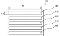
- FIG. 3A is a diagram illustrating a front side of the solar cell unit 100 according to the first embodiment
- FIG. 3B is a diagram illustrating a rear side of the solar cell unit 100 according to the first embodiment
- FIG. 5 is a side sectional view taken along a broken line AA shown in FIG. 4 of the solar cell unit 100 according to the first embodiment.
- FIG. 5 is a side sectional view taken along a broken line BB shown in FIG. 4 of the solar cell unit 100 according to the first embodiment.
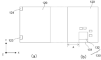
- FIG. 2A is a diagram illustrating a front surface of a substrate 120 according to the first embodiment
- FIG. 2B is a diagram illustrating a back surface of the substrate 120 according to the first embodiment.
- FIG. 3A is a diagram illustrating the front side of the solar cell 110 according to the first embodiment
- FIG. 3B is a diagram illustrating the rear side of the solar cell 110 according to the first embodiment.
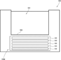
- FIG. 3 is an enlarged view of a communication antenna 131 of the solar cell unit 100 according to the first embodiment. It is an image figure showing rack 500 concerning a 3rd embodiment.
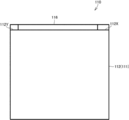
- FIG. 11 is a rear view showing a first glass substrate 111 and a second glass substrate 112 of a solar cell 110 according to a fourth embodiment. It is a side view showing the 1st glass substrate 111, the 2nd glass substrate 112, and substrate 120 of solar cell 110 concerning a 4th embodiment.
- the solar cell unit 100 is installed in a passage where people come and go or a wall 300 of a room.
- the solar cell unit 100 is installed at a position of 130 cm or more from the floor 400 or the ground, and preferably at a height of about 150 cm, so that light from indoor lights is easily received and light is not likely to be blocked by a person. Is done.
- the solar cell unit 100 mounts a solar cell 110 having a plurality of vertically elongated cells 115, 115.
- the cell 115 is substantially rectangular. Are arranged side by side in the short direction. Are connected in series with each other.
- the solar cell unit 100 according to the present embodiment is fixed to a wall, a column, or the like so that the vertical direction of the cells 115, 115,...
- solar cell unit 100 mainly includes a solar cell 110, a substrate 120, and a communication unit 130 of Bluetooth (registered trademark). And Solar cell 110 is mounted on the surface of substrate 120.
- the communication unit 130 includes a communication antenna 131 and a control IC 132 for controlling a signal interval and a signal strength transmitted by the communication antenna 131, and is attached to the back surface of the board 120.
- electronic components such as a power storage element for storing the power generated by the solar cell 110, wiring (not shown) for electrically connecting each electronic component, and the like are provided. It is installed.
- the solar cell unit 100 performs various kinds of communication by the communication unit 130 using the electric power generated by the solar cell 110.
- a signal e.g., Bluetooth (registered trademark)
- a terminal such as a mobile phone can accurately acquire its own position, or a server or the like can accurately acquire the position of the terminal.
- the solar cell 110 includes a first glass substrate 111 and a second glass substrate 112.
- a transparent conductive film is formed on the first glass substrate 111 on the second glass substrate 112 side.
- notches 112X and 112Y are formed at both ends in the Y direction and one end in the X direction in FIG. 8 of the second glass substrate 112, respectively.
- the cutout portion 112X a portion of the first glass substrate 111 where the transparent conductive film is exposed becomes the negative electrode output terminal 113
- the cutout portion 112Y the first glass The portion of the substrate 111 where the transparent conductive film is exposed becomes the positive electrode output terminal 114. That is, the negative electrode output terminal 113 and the positive electrode output terminal 114 are formed on the back surface of the solar cell 110, that is, on the substrate 120 side.
- solar cell 110 is a dye-sensitized solar cell having a monolithic structure. As shown in FIG. 4, when viewed from the surface of the solar cell 110, a plurality of vertically long cells 115, 115... Are arranged side by side in the lateral direction. In the cell 115, a semiconductor layer containing a dye and semiconductor particles, an insulating layer, and a counter electrode conductive layer are stacked over a transparent conductive film. The transparent conductive film of the cell 115 is insulated from the transparent conductive film of the adjacent cell 115, and the counter electrode conductive layer of the cell 115 is electrically connected to the transparent conductive film of the adjacent cell 115 so that the two adjacent cells 115 Are connected in series with each other. More specifically, solar cell 110 according to the present embodiment has a total output of 3 volts by connecting five cells 115 having an electromotive force of 0.6 volts in series.
- a negative input terminal 123 is attached to the surface of the substrate 120 at a position facing the negative output terminal 113 of the solar cell 110, and the positive output of the solar cell 110 is provided.
- a positive input terminal 124 is attached at a position facing the terminal 114.
- the area of the back surface of the portion where the minus pole input terminal 123 and the plus pole input terminal 124 are provided has a flat area. Is formed.
- the flat area includes an end portion of the substrate 120 where the minus pole input terminal 123 and the plus pole input terminal 124 are located in the Y-axis direction in FIG. Preferably, there is.
- the electronic component is arranged from the opposite end to a position at least A of A mm away. It is preferable to keep it flat.
- the degree of flatness does not need to be flat to about 1 ⁇ m or 1 nm, and is not more than 1/10, more preferably less than 1/20, relative to the size of the substrate 120, for example, Amm. Good.
- the substrate 120 can be stably held by placing the substrate 120 on the flat table 200 with the flat area facing down, and work on the surface of the substrate 120 can be performed. Performance can be improved.
- the heights of the surfaces of the projections need only be about the same, and the substrate 120 is placed on the flat table 200 with the area down. By doing so, the substrate 120 can be stably held, and workability on the surface of the substrate 120 can be improved.
- FIG. 9 is an enlarged view of the area C indicated by the broken line in FIG. 4, and is an enlarged view of the communication antenna 131.
- the longitudinal direction of communication antenna 131 is configured to be parallel to the edge of substrate 120.
- the communication antenna 131 includes an antenna body, that is, a director 133, and a support plate 134 for supporting the director 133 having low rigidity.
- the support plate 134 is configured so that the longitudinal direction is along the edge of the substrate 120.
- all or a part of the director 133 may be configured so as to be parallel to the edge of the substrate 120 and along the edge of the substrate 120. That is, it is preferable that the long part of the director 132 is arranged in parallel with the edge of the substrate 120.
- the solar cell unit 100 reduces the possibility that power generation cannot be performed even when a person stops right before, and the possibility that transmission of radio waves from the communication antenna 131 may be interrupted. Can be reduced.
- the communication antenna 131 transmits a signal or the like using Bluetooth (registered trademark). However, it is not limited to such a form.
- the communication antenna 131 may perform wireless communication using WiFi (registered trademark).
- an LED light that emits infrared light may be mounted on the substrate 120 instead of or in addition to the communication unit 130. Then, for example, the control IC 132 may cause the LED lights to output infrared rays according to predetermined conditions.
- a plurality of larger cells 115 may be used as shown in FIG. ⁇ Third embodiment>
- the solar cell unit 100 is mounted on a wall or a pillar. However, it is not limited to such a form.
- the solar cell unit 100 may be mounted on a rack 500 or a shelf of a product.
- the rack 500 includes an opening 501 for accommodating various parts and products, a wall surface 502 for forming the opening 501, and a solar cell unit 100B attached to the wall surface 502. It is preferable that the solar cell unit 100B is attached to the wall surface 502 so that the solar cell 110 faces upward, obliquely upward, or the front, that is, in a direction in which the light is installed.
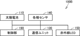
- the solar cell unit 100B includes a communication antenna 131 for Bluetooth (registered trademark) or WiFi (registered trademark), a proximity sensor, an infrared sensor, or the like. It has various sensors 140 and a control unit 190 for controlling each unit of the solar cell unit 100B. As described above, the solar cell units 100 and 100B may have the infrared LED 150 instead of or in addition to the communication unit 130.
- the arrangement method of the cells 115, 115... Of the solar cell unit 100B is adjusted based on the direction in which the shopper of the product points his hand.
- the solar cell 110 and the solar cell unit 100 are arranged so that the longitudinal direction of the cells 115, 115,. Preferably, it is attached.
- the control unit 190 or the like transmits a user or a customer via various sensors 140 such as a proximity sensor or an infrared sensor. Detects that a part or rack has been taken out by inserting a hand through the opening 501, and the information can be provided to the control device via the communication unit 130. Moreover, since the longitudinal direction of the cells 115, 115,... Is arranged substantially at right angles to the direction of the arm, the possibility that any of the cells 115 is completely hidden by the arm can be reduced. That is, it is possible to reduce the possibility that the solar cell unit 100 cannot generate power due to the inability of any of the cells 115 to generate power, or the necessary information cannot be transmitted or received. ⁇ Fourth embodiment>
- the second glass substrate 112 may be cut not only at the notches 112X and 112Y but also at the entire end. That is, as shown in FIGS. 12 and 13, the first glass substrate 111 and the second glass substrate 112 are offset such that the edge of the second glass substrate 112 is inward of the edge of the first glass substrate 111. It may be stuck so that it does.
- the solar cell unit 100 after the first glass substrate 111 and the second glass substrate 112 are bonded together, the first glass substrate 111 and the first glass substrate Between the glass substrate 111 and the second glass substrate 112 is injected. Then, an ultraviolet curable resin 116 is applied to the back surface of the first glass substrate 111 and the side surface of the second glass substrate 112 so as to cover the inlet for the electrolyte. At this time, the ultraviolet curable resin 116 is not applied to the notches 112X and 112Y.
- the dye-sensitized solar cell 110 has been described, but another type of solar cell may be used.
- the communication antenna 130 is disposed at one end of the substrate 120 in the longitudinal direction of the cells 115, 115,... Of the solar cells 110, and the cells 115, 115,. .. Have the minus pole input terminal 123 and the plus pole input terminal 124 at the other end in the longitudinal direction, but the communication antenna 131 is arranged at one short side end of the cells 115 of the solar cell 110.
- a negative pole input terminal 123 and a positive pole input terminal 124 may be arranged at the other ends of the cells 115 of the solar cell 110 in the lateral direction.
- the electronic device includes the substrate 120, the solar cell 110 attached to the substrate 120, and the output unit for transmitting radio waves by the electric power from the solar cell 110.
- the solar cell 110 includes a plurality of cells 115, 115,... Are arranged side by side in the lateral direction.
- the output unit 130 emits communication radio waves for short distances.
- the output unit 150 emits infrared light.
- an installation method is provided in which the solar cell unit 100 is installed indoors such that the longitudinal direction of the plurality of cells 115 is substantially horizontal.
- an installation method is provided in which the solar cell unit 100 is installed at a height of 130 cm or more from the floor.
- solar cell unit 100B solar cell unit 110: dye-sensitized solar cell 111: first glass substrate 112: second glass substrate 112X: cutout portion 112Y: cutout portion 113: minus pole output terminal 114: plus Pole output terminal 115: Cell 116: UV curable resin 120: Substrate 123: Negative pole input terminal 124: Positive pole input terminal 130: Communication unit 131: Communication antenna 132: Control IC 133: director 134: support plate 140: sensor 150: infrared LED 190: control unit 300: wall 400: floor 500: rack 501: opening 502: wall surface
Landscapes
- Photovoltaic Devices (AREA)
Abstract
基板(120)と、基板(120)に取り付けられる太陽電池(110)と、太陽電池(110)からの電力によって電波を発信するための出力部(130)とを備える。太陽電池(110)は、複数のセル(115,115・・・)を含む。複数のセル(115,115・・・)は、互いに短手方向に並べて配置される。
Description
本国際出願は、2018年7月24日に日本国特許庁に出願された日本国特許出願第2018-138847号に基づく優先権を主張するものであり、日本国特許出願第2018-138847号の全内容を参照により本国際出願に援用する。
以下の開示は、太陽電池を搭載した太陽電池ユニットの技術に関する。
従来から、太陽電池や通信アンテナを搭載した太陽電池ユニットが知られている。たとえば、国際公報第2017/013940号パンフレット(特許文献1)には、通信装置が開示されている。特許文献1によると、照射光を受光する受光面を有する太陽電池と、上記受光面の裏面上に設置される蓄電デバイスと、通信用アンテナを有し、上記蓄電デバイスの上記太陽電池との対向面の裏面上に設置される回路基板と、を備える、通信装置が提供される。
本開示の目的は、使い勝手のよい太陽電池ユニットおよびその設置方法を提供することにある。
本開示の一態様に従うと、基板と、基板に取り付けられる太陽電池と、太陽電池からの電力によって電波を発信するための出力部とを備える太陽電池ユニットが提供される。太陽電池は、複数のセルを含む。複数のセルは、互いに短手方向に並べて配置される。
以上のように、本開示によれば、使い勝手のよい太陽電池ユニットおよびその設置方法が提供される。
以下、図面を参照しつつ、本開示の実施の形態について説明する。以下の説明では、同一の部品には同一の符号を付してある。それらの名称および機能も同じである。したがって、それらについての詳細な説明は繰り返さない。
<第1の実施の形態>
<太陽電池ユニット100の概要>
<第1の実施の形態>
<太陽電池ユニット100の概要>
図1に示すように、本実施の形態にかかる太陽電池ユニット100は、人が行き交う通路や部屋の壁300に設置される。たとえば、太陽電池ユニット100は、室内のライトからの光を受けやすく、人によって光を遮られる可能性が低いように、床400や地面から130cm以上の位置、好ましくは150cm程度の高さに設置される。
特に本実施の形態においては、図1および図2に示すように、太陽電池ユニット100は、複数の縦長のセル115,115・・・を有する太陽電池110を搭載する。セル115は、略方形である。セル115,115・・・はお互いに短手方向に並べて配置される。そして、セル115,115・・・は互いに直列に接続される。また本実施の形態にかかる太陽電池ユニット100は、壁への設置作業において、セル115,115・・・の縦長方向が略水平方向となるように、壁や柱などに固定される。
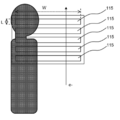
これによって、仮に図3に示すように、通行人などが太陽電池ユニット100の直前に立ち止まっても、いずれかのセル115が当該人によって完全に隠れてしまう可能性を低減することができる。すなわち、いずれかのセル115が発電できなくなることによって太陽電池ユニット100が発電できなくなったり、所定の動作が実行できなくなったりすることを低減することができる。
<太陽電池ユニット100の全体構成>
<太陽電池ユニット100の全体構成>
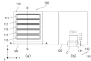
本実施の形態にかかる太陽電池ユニット100の全体構成について説明する。図4から図9を参照して、本実施の形態にかかる太陽電池ユニット100は、主に、太陽電池110と、基板120と、Bluetooth(登録商標)の通信ユニット130を含む。とを含む。太陽電池110は、基板120の表面に取り付けられる。通信ユニット130は、通信用アンテナ131と通信用アンテナ131が発信する信号間隔や信号強度を制御する制御IC132を含み、基板120の裏面に取り付けられる。基板120の裏面には、通信ユニット130の他に、太陽電池110が生み出した電力を蓄電する蓄電素子などの電子部品や、各電子部品を電気的に接続するための配線(不図示)などが取りつけられている。
本実施の形態にかかる太陽電池ユニット100は、太陽電池110で生み出した電力を利用して、通信ユニット130によって各種の通信を行うものである。たとえば、太陽電池110として色素増感太陽電池を利用し、通信ユニット130としてビーコンを利用することによって、屋内のライトからの光によって発電しながら、Bluetooth(登録商標)による信号などを定期的に発することができる。これによって、携帯電話などの端末が自身の位置を正確に取得したり、サーバなどで端末の位置を正確に取得したりすることができる。
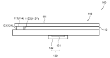
より詳細には、太陽電池110は、第1のガラス基板111と、第2のガラス基板112とを含む。第1のガラス基板111の、第2のガラス基板112側には、透明導電膜が形成されている。そして、第2のガラス基板112の、図8におけるY方向の両端かつX方向の一端にそれぞれ切り欠き部112X,112Yが形成される。そして、切り欠き部112Xが形成されることで、第1のガラス基板111の透明導電膜が露出した部分がマイナス極出力端子113となり、切り欠き部分112Yが形成されることで、第1のガラス基板111の透明導電膜が露出した部分がプラス極出力端子114となる。つまり、太陽電池110の裏面、すなわち基板120側に、マイナス極出力端子113とプラス極出力端子114とが形成される。
なお、本実施の形態においては、太陽電池110は、モノリシック構造を有する色素増感太陽電池である。図4に示すように、太陽電池110の表面視において、複数の縦長のセル115,115・・・が短手方向に並べて配置されるものである。セル115は、透明導電膜上に色素および半導体粒子を含む半導体層と、絶縁層と、対極導電層が積層されている。セル115の透明導電膜は隣接するセル115の透明導電膜と絶縁され、セル115の対極導電層は隣接するセル115の透明導電膜と電気的に接続されることで、隣接した2つのセル115が互いに直列に接続されている。より詳細には、本実施の形態にかかる太陽電池110は、0.6ボルトの起電力を有するセル115を、5個直列につないで、全体的に3ボルトの出力を有する。
図5および図7(a)に示すように、基板120の表面には、太陽電池110のマイナス極出力端子113に対向する位置にマイナス極入力端子123が取り付けられ、太陽電池110のプラス極出力端子114に対向する位置にプラス極入力端子124が取り付けられる。
そして特に、本実施の形態においては、図7(b)に示すように、基板120の裏側においては、マイナス極入力端子123およびプラス極入力端子124が設けられている部分の裏面はエリアがフラットに形成されている。
なお、フラットなエリアは、図7のY軸方向において、マイナス極入力端子123およびプラス極入力端子124が位置する基板120の端部を含み、基板120全体の1/3以上のまとまったエリアであることが好ましい。換言すれば、通信用アンテナ131が配置されている端部から、該端部までの距離をAmmとすると、当該逆の端部からAmmの1/3以上離れた位置までを電子部品が配置されていないフラットにしておくことが好ましい。
また、フラットの程度は、1μmや1nm程度までフラットにする必要はなく、基板120の大きさ、たとえばAmmに対して、1/10未満の凹凸、より好ましくは1/20未満の凹凸であればよい。これによって、図4に示すように、当該フラットなエリアを下にして基板120をフラットな台200に載置することによって、基板120を安定して保持することができ、基板120の表面に対する作業性を向上させることができる。
より詳細には、対象となるエリアに大きな凹凸があったとしても、凸部同士の表面の高さが同程度であればよく、当該エリアを下にして基板120をフラットな台200に載置することによって、基板120を安定して保持することができ、基板120の表面に対する作業性を向上させることができる。
図6が示すように、基板120は、第1のガラス基板111および第2のガラス基板112の一端から突出している部分を有する。通信用アンテナの131は、太陽電池110の表面視において、少なくとも通信用アンテナ131の一部が第1のガラス基板111および第2のガラス基板112と重ならないように、基板120が第1のガラス基板111および第2のガラス基板120の一端から突出している部分の裏面に設けられている。さらに、図7が示すように、通信用アンテナ131の縁が基板120の縁に重なるように配置されている。これによって、通信用アンテナ131が発信する信号が表面に積層されている太陽電池110によって減衰されることを抑制している。
図9は、図4の破線で示された領域Cの拡大した図であり、通信用アンテナ131を拡大した図である。本実施の形態においては、図9が示すように、通信用アンテナ131の長手方向が、基板120の縁と平行に構成されている。図9に示すように、通信用アンテナ131は、アンテナ本体すなわち導波器133と、剛性が弱い導波器133を支持するための支持プレート134とを含む。本実施の形態においては、支持プレート134の長手方向が、基板120の縁に沿うように構成される。
ただし、導波器133の全部または一部が、基板120の縁に平行に、基板120の縁に沿うように構成されてもよい。つまり導波器132の長尺部分が、基板120の縁に平行に配置されることが好ましい。
このように構成されるため、本実施の形態にかかる太陽電池ユニット100は、直前に人が立ち止まっても発電ができなくなる可能性を低減し、通信用アンテナ131からの電波の発信が途絶える可能性を低減することができる。
<第2の実施の形態>
<第2の実施の形態>
上記の実施の形態においては、通信用アンテナ131は、Bluetooth(登録商標)を利用して信号などを発信するものであった。しかしながら、このような形態には限られない。たとえば、通信用アンテナ131は、WiFi(登録商標)による無線通信を行ってもよい。
あるいは、基板120には、通信ユニット130の代わりに、あるいは通信ユニット130に加えて、赤外線を発するLEDライトを搭載してもよい。そしてたとえば、制御IC132が、所定の条件に合わせて、LEDライトに赤外線を出力させてもよい。
また、起電力が足りない場合には、図11に示すように、より大きな複数のセル115,115・・・を利用してもよい。
<第3の実施の形態>
<第3の実施の形態>
上記の実施の形態においては、太陽電池ユニット100は、壁や柱に取り付けられるものであった。しかしながら、このような形態には限られない。
たとえば、図10に示すように、商品のラック500や棚などに太陽電池ユニット100を取り付けもよい。より詳細には、ラック500は、各種のパーツや商品を収容するための開口部501と、開口部501を形成するための壁面502と、壁面502に取り付けられる太陽電池ユニット100Bとを含む。太陽電池ユニット100Bは、太陽電池110が上方または斜め上方または正面など、すなわちライトが設置される向き、に向くように壁面502に取り付けられることが好ましい。
より詳細には、本実施の形態にかかる太陽電池ユニット100Bは、図11に示すように、Bluetooth(登録商標)やWiFi(登録商標)用の通信用アンテナ131や、近接センサや赤外線センサなどの各種センサ140や、太陽電池ユニット100Bの各部を制御するための制御部190を有する。なお、上述したように、太陽電池ユニット100,100Bは、通信ユニット130の代わりに、または通信ユニット130に加えて赤外線LED150を有してもよい。
この場合は、当該商品の買い物客が手を指し伸ばす方向に基づいて、太陽電池ユニット100Bのセル115,115・・・の配置方法を調節する。一例としては、買い物客がラック内に手を差し入れたときに、腕の方向と略直角にセル115,115・・・の長手方向が配置されるように、太陽電池110や太陽電池ユニット100が取り付けられることが好ましい。
このように、ラック500や棚などに太陽電池ユニット100が取り付けられるため、本実施の形態においては、制御部190などが、近接センサや赤外線センサなどの各種センサ140を介して、ユーザや客などが開口部501から手を差し込んでパーツやラックを取り出したことを検知して、通信ユニット130を介して当該情報を制御装置に提供することができる。しかも、腕の方向と略直角にセル115,115・・・の長手方向が配置されるため、いずれかのセル115が腕によって完全に隠れてしまう可能性を低減することができる。すなわち、いずれかのセル115が発電できなくなることによって太陽電池ユニット100が発電できなくなったり、必要な情報が送受信できなくなったりすることを低減することができる。
<第4の実施の形態>
<第4の実施の形態>
上記の実施の形態に加えて、第2のガラス基板112は、切り欠き部112X,112Yだけでなく、端部全体が切りかかれていてもよい。すなわち、図12および図13に示すように、第1のガラス基板111と第2のガラス基板112とが、第2のガラス基板112の縁が第1のガラス基板111の縁よりも内側にオフセットするように張り付けられてもよい。
より詳細には、本実施の形態にかかる太陽電池ユニット100に関しては、第1のガラス基板111と第2のガラス基板112とを貼り合わせた後に、上記のように両者のズレた部分から第1のガラス基板111と第2のガラス基板112との間に電解液を注入する。そして、電解液の注入口をふさぐように、第1のガラス基板111の裏面と第2のガラス基板112の側面に紫外線硬化性樹脂116を塗布する。このとき、切り欠き部112X,112Yには、紫外線硬化性樹脂116を塗布しない。
そして、紫外線硬化性樹脂116が固まると、紫外線硬化性樹脂116が第2のガラス基板112の表面よりも基板120側に飛び出さないように、紫外線硬化性樹脂116の表面を斜めに削り落とす。これによって、太陽電池110の端部と基板120の端部との間に隙間が生じ、より作業性が向上する。
<第5の実施の形態>
<第5の実施の形態>
上記の実施の形態においては、色素増感太陽電池110に関して説明を行ったが、他の種類の太陽電池であってもよい。また、上記の実施の形態においては、基板120のうちの、太陽電池110のセル115,115・・・の長手方向の一端に通信用アンテナ130を配置し、太陽電池110のセル115,115・・・の長手方向の他端にマイナス極入力端子123およびプラス極入力端子124を配置したが、太陽電池110のセル115,115・・・の短手方向の一端に通信用アンテナ131を配置し、太陽電池110のセル115,115・・・の短手方向の他端にマイナス極入力端子123およびプラス極入力端子124を配置してもよい。
<まとめ>
<まとめ>
上記の実施の形態においては、基板120と、基板120に取り付けられる太陽電池110と、太陽電池110からの電力によって電波を発信するための出力部とを備える。太陽電池110は、複数のセル115,115・・・を含む。複数のセル115,115・・・は、互いに短手方向に並べて配置される。
好ましくは、出力部130は近距離用の通信電波を発する。
好ましくは、出力部150は赤外線を発する。
上記の実施の形態においては、太陽電池ユニット100を、複数のセル115,115・・・の長手方向が略水平方向になるように屋内に設置する、設置方法が提供される。
上記の実施の形態においては、太陽電池ユニット100を、床から130cm以上の高さに設置する、設置方法が提供される。
今回開示された実施の形態はすべての点で例示であって制限的なものではないと考えられるべきである。本開示の範囲は、上記した説明ではなく、特許請求の範囲によって示され、特許請求の範囲と均等の意味および範囲内でのすべての変更が含まれることが意図される。
100 :太陽電池ユニット
100B :太陽電池ユニット
110 :色素増感太陽電池
111 :第1のガラス基板
112 :第2のガラス基板
112X :切り欠き部
112Y :切り欠き部
113 :マイナス極出力端子
114 :プラス極出力端子
115 :セル
116 :紫外線硬化性樹脂
120 :基板
123 :マイナス極入力端子
124 :プラス極入力端子
130 :通信ユニット
131 :通信用アンテナ
132 :制御IC
133 :導波器
134 :支持プレート
140 :センサ
150 :赤外線LED
190 :制御部
300 :壁
400 :床
500 :ラック
501 :開口部
502 :壁面
100B :太陽電池ユニット
110 :色素増感太陽電池
111 :第1のガラス基板
112 :第2のガラス基板
112X :切り欠き部
112Y :切り欠き部
113 :マイナス極出力端子
114 :プラス極出力端子
115 :セル
116 :紫外線硬化性樹脂
120 :基板
123 :マイナス極入力端子
124 :プラス極入力端子
130 :通信ユニット
131 :通信用アンテナ
132 :制御IC
133 :導波器
134 :支持プレート
140 :センサ
150 :赤外線LED
190 :制御部
300 :壁
400 :床
500 :ラック
501 :開口部
502 :壁面
Claims (7)
- 基板と、
前記基板に取り付けられる太陽電池と、
前記太陽電池からの電力によって電波を発信するための出力部とを備え、
前記太陽電池は、複数のセルを含み、
前記複数のセルは、互いに短手方向に並べて配置される、太陽電池ユニット。 - 前記出力部は近距離用の通信電波を発する、請求項1に記載の太陽電池ユニット。
- 前記出力部は、通信用アンテナを備え、
前記通信用アンテナの長手方向が、前記複数のセルの短手方向に沿って、配置されている、請求項1または2に記載の太陽電池ユニット。 - 前記通信用アンテナは前記基板の縁に接して配置されている、請求項3に記載の太陽電池ユニット。
- 前記出力部は赤外線を発する、請求項1から4のいずれか1項に記載の太陽電池ユニット。
- 請求項1に記載の太陽電池ユニットを、前記複数のセルの長手方向が略水平方向になるように屋内に設置する、設置方法。
- 請求項1に記載の太陽電池ユニットを、床から130cm以上の高さに設置する、設置方法。
Applications Claiming Priority (2)
| Application Number | Priority Date | Filing Date | Title |
|---|---|---|---|
| JP2018138847A JP2021168317A (ja) | 2018-07-24 | 2018-07-24 | 太陽電池ユニットおよび設置方法 |
| JP2018-138847 | 2018-07-24 |
Publications (1)
| Publication Number | Publication Date |
|---|---|
| WO2020021862A1 true WO2020021862A1 (ja) | 2020-01-30 |
Family
ID=69180479
Family Applications (1)
| Application Number | Title | Priority Date | Filing Date |
|---|---|---|---|
| PCT/JP2019/021919 Ceased WO2020021862A1 (ja) | 2018-07-24 | 2019-06-03 | 太陽電池ユニットおよび設置方法 |
Country Status (2)
| Country | Link |
|---|---|
| JP (1) | JP2021168317A (ja) |
| WO (1) | WO2020021862A1 (ja) |
Citations (6)
| Publication number | Priority date | Publication date | Assignee | Title |
|---|---|---|---|---|
| US20110319137A1 (en) * | 2010-06-25 | 2011-12-29 | Sony Ericsson Mobile Communications Japan, Inc. | Portable device |
| JP2015056293A (ja) * | 2013-09-12 | 2015-03-23 | 株式会社フジクラ | 色素増感太陽電池素子 |
| US20170040801A1 (en) * | 2015-08-04 | 2017-02-09 | Goal Zero Llc | Portable solar panel system electrical control |
| WO2017146074A1 (ja) * | 2016-02-26 | 2017-08-31 | シャープ株式会社 | 太陽電池を用いた電源装置、それを備える通信装置等の電子装置、および看板装置 |
| WO2017154601A1 (ja) * | 2016-03-08 | 2017-09-14 | 株式会社フジクラ | 光電変換装置 |
| JP2017216766A (ja) * | 2016-05-30 | 2017-12-07 | 大日本印刷株式会社 | 太陽電池受光面用の印刷画像作成装置 |
-
2018
- 2018-07-24 JP JP2018138847A patent/JP2021168317A/ja active Pending
-
2019
- 2019-06-03 WO PCT/JP2019/021919 patent/WO2020021862A1/ja not_active Ceased
Patent Citations (6)
| Publication number | Priority date | Publication date | Assignee | Title |
|---|---|---|---|---|
| US20110319137A1 (en) * | 2010-06-25 | 2011-12-29 | Sony Ericsson Mobile Communications Japan, Inc. | Portable device |
| JP2015056293A (ja) * | 2013-09-12 | 2015-03-23 | 株式会社フジクラ | 色素増感太陽電池素子 |
| US20170040801A1 (en) * | 2015-08-04 | 2017-02-09 | Goal Zero Llc | Portable solar panel system electrical control |
| WO2017146074A1 (ja) * | 2016-02-26 | 2017-08-31 | シャープ株式会社 | 太陽電池を用いた電源装置、それを備える通信装置等の電子装置、および看板装置 |
| WO2017154601A1 (ja) * | 2016-03-08 | 2017-09-14 | 株式会社フジクラ | 光電変換装置 |
| JP2017216766A (ja) * | 2016-05-30 | 2017-12-07 | 大日本印刷株式会社 | 太陽電池受光面用の印刷画像作成装置 |
Also Published As
| Publication number | Publication date |
|---|---|
| JP2021168317A (ja) | 2021-10-21 |
Similar Documents
| Publication | Publication Date | Title |
|---|---|---|
| US11503143B2 (en) | Handheld electronic device | |
| EP3832993B1 (en) | Handheld electronic device | |
| EP3832797B1 (en) | Handheld electronic device | |
| CN104067163B (zh) | 包括多功能和通信表面的显示设备 | |
| US10554868B2 (en) | Camera module and mobile terminal | |
| CN108803164B (zh) | 一种显示装置 | |
| EP3832748A1 (en) | Display panel and manufacturing method therefor | |
| CN107393458A (zh) | 一种柔性显示面板及装置 | |
| US20180158382A1 (en) | Information transmitting apparatus | |
| JP2017053821A (ja) | 放射線撮像装置 | |
| WO2020021862A1 (ja) | 太陽電池ユニットおよび設置方法 | |
| CN114188378B (zh) | 一种阵列基板、显示面板以及显示装置 | |
| US8879018B2 (en) | Electronic apparatus and display thereof | |
| CN110896093A (zh) | 输入感测单元和包括该输入感测单元的显示设备 | |
| JP6975859B2 (ja) | 太陽電池ユニットおよび太陽電池ユニットを備えた無線発信機 | |
| CN209590811U (zh) | 一种防静电触摸显示装置 | |
| CN106991313B (zh) | 显示屏、显示装置及电子设备 | |
| KR101189070B1 (ko) | 염료감응형 태양전지와 led 보드를 포함하는 방음벽 |
Legal Events
| Date | Code | Title | Description |
|---|---|---|---|
| 121 | Ep: the epo has been informed by wipo that ep was designated in this application |
Ref document number: 19841750 Country of ref document: EP Kind code of ref document: A1 |
|
| NENP | Non-entry into the national phase |
Ref country code: DE |
|
| 122 | Ep: pct application non-entry in european phase |
Ref document number: 19841750 Country of ref document: EP Kind code of ref document: A1 |
|
| NENP | Non-entry into the national phase |
Ref country code: JP |