WO2020021594A1 - アンテナ装置 - Google Patents
アンテナ装置 Download PDFInfo
- Publication number
- WO2020021594A1 WO2020021594A1 PCT/JP2018/027488 JP2018027488W WO2020021594A1 WO 2020021594 A1 WO2020021594 A1 WO 2020021594A1 JP 2018027488 W JP2018027488 W JP 2018027488W WO 2020021594 A1 WO2020021594 A1 WO 2020021594A1
- Authority
- WO
- WIPO (PCT)
- Prior art keywords
- plate
- antenna device
- length
- conductor
- parallel
- Prior art date
- Legal status (The legal status is an assumption and is not a legal conclusion. Google has not performed a legal analysis and makes no representation as to the accuracy of the status listed.)
- Ceased
Links
Images






Classifications
-
- H—ELECTRICITY
- H01—ELECTRIC ELEMENTS
- H01Q—ANTENNAS, i.e. RADIO AERIALS
- H01Q13/00—Waveguide horns or mouths; Slot antennas; Leaky-waveguide antennas; Equivalent structures causing radiation along the transmission path of a guided wave
- H01Q13/10—Resonant slot antennas
-
- H—ELECTRICITY
- H01—ELECTRIC ELEMENTS
- H01Q—ANTENNAS, i.e. RADIO AERIALS
- H01Q21/00—Antenna arrays or systems
- H01Q21/06—Arrays of individually energised antenna units similarly polarised and spaced apart
Definitions
- the present invention relates to an antenna device.
- TSA Tapered Slot Antenna
- Patent Literature 1 describes a parallel plate-loaded TSA.
- the parallel plate-loaded TSA can easily match with the power supply system even if the antenna aperture is reduced to a half wavelength or less at the upper limit frequency of the frequency band used for transmission and reception.
- radio waves are re-emitted from adjacent element antennas, and a radiation pattern obtained when each of a plurality of element antennas constituting the array antenna is excited by one element, that is, a beam of the array element pattern
- the width becomes narrow.
- the beam width of the array element pattern is reduced, there is a problem in that the gain decrease during beam scanning becomes large depending on the area covered by the array antenna.
- the present invention has been made to solve the above problems, and an object of the present invention is to provide an antenna device that can suppress radio wave leakage between element antennas straddling a parallel plate when used as an element antenna of an array antenna.
- the antenna device has a parallel plate, which is a pair of conductor plates arranged in parallel with each other, and a first surface to which both the pair of conductor plates are electrically connected.
- the length from the first surface to the end of the parallel plate along the direction normal to the first surface of the conductor short-circuit plate is the first length along the direction normal to the first surface. It is longer than the length from the first surface to the end of the tapered conductor plate. This makes it possible to suppress the leakage of radio waves between the element antennas straddling the parallel plate.
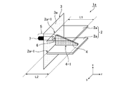
- FIG. 2 is a perspective view showing a configuration of the antenna device according to the first embodiment.
- FIG. 3 is a perspective view showing a configuration of an element antenna in the antenna device according to Embodiment 1.
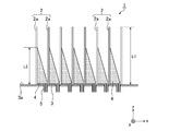
- FIG. 2 is a diagram illustrating the antenna device as viewed in the + y direction in FIG. 1.
- FIG. 2 is a diagram illustrating the antenna device as viewed in the ⁇ x direction of FIG. 1.
- FIG. 2 is a diagram illustrating the antenna device as viewed in the ⁇ z direction of FIG. 1. It is a graph which shows the average value of all elements of a radiation pattern of a radio wave.
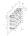
- FIG. 7 is a perspective view showing a configuration of a modification of the antenna device according to Embodiment 1.
- FIG. 1 is a perspective view showing a configuration of a modification of the antenna device according to Embodiment 1.
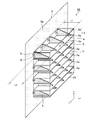
- FIG. 9 is a perspective view illustrating a configuration of an antenna device according to a second embodiment.
- FIG. 13 is a perspective view showing a configuration of a modification of the antenna device according to the second embodiment.
- FIG. 9 is a diagram illustrating a configuration of an antenna device according to a third embodiment.
- FIG. 14 is a diagram illustrating a configuration of a modification of the antenna device according to the third embodiment.
- FIG. 14 is a diagram illustrating a configuration of another modification of the antenna device according to the third embodiment.
- FIG. 14 is a front view showing an element antenna array in the antenna device according to Embodiment 4.
- FIG. 15 is a front view showing an element antenna array in a modification of the antenna device according to the fourth embodiment.
- FIG. 21 is a front view showing an element antenna array in another modification of the antenna device according to Embodiment 4.
- FIG. 21 is a front view showing an element antenna array in still another modification of the antenna device according to Embodiment 4.
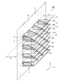
- FIG. 1 is a perspective view showing a configuration of the antenna device 1 according to the first embodiment, and shows a case where the antenna device 1 is an array antenna.
- FIG. 2 is a perspective view showing a configuration of the element antenna 1a in the antenna device 1.
- the antenna device 1 is an array antenna, but the antenna device 1 may be a single element antenna 1a shown in FIG. 1 and 2, the uppermost conductive plate 2a is shown transparent so that the tapered conductive plate 4 provided on the parallel plate 2 can be seen.
- FIG. 3 is a diagram showing the antenna device 1 as viewed in the + y direction of FIG.
- FIG. 4 is a diagram illustrating the antenna device 1 as viewed in the ⁇ x direction of FIG. In FIG.
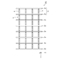
- FIG. 5 is a diagram illustrating the antenna device 1 as viewed in the ⁇ z direction of FIG.
- the antenna device 1 includes a plurality of parallel flat plates 2, a conductor short-circuit plate 3, and a plurality of tapered conductive plates 4.
- the parallel flat plate 2 is a pair of conductive flat plates 2a, 2a arranged in parallel with each other. 1, 3, 4, and 5, among the plurality of conductive flat plates 2 a arranged in parallel, the adjacent conductive flat plate 2 a and the conductive flat plate 2 a are all parallel flat plates 2.
- the conductor short-circuit plate 3 is a conductor plate member at a ground potential, and the surface 3a of the conductor short-circuit plate 3 is a first surface to which both the pair of conductor flat plates 2a, 2a are electrically connected.
- the tapered conductive plate 4 is provided between the pair of conductive flat plates 2a, 2a and along a plane parallel to the normal direction of the surface 3a and the normal direction of the conductive flat plate 2a. It has a shape in which the conductor width decreases along the direction (x direction). 1 to 5, the flat plate surface of the conductive flat plate 2a is provided in parallel with the yz plane, and the flat plate surface of the tapered conductive plate 4 is provided in parallel with the zx plane.
- the radiation direction is the + z direction.
- the normal direction in the first embodiment may be a direction in an angle range in which an angle with respect to the surface can be approximated to a direction orthogonal to the surface, in addition to the direction perpendicular to the surface.
- the respective end faces 2a-1 of the pair of conductor flat plates 2a, 2a, which are the parallel flat plates 2, are end faces facing the surface 3a of the conductor short-circuit plate 3.
- the end face 2a-1 is electrically connected to the face 3a as shown in FIG.
- the parallel flat plate 2, which is a pair of conductive flat plates 2 a, 2 a, is short-circuited on the surface 3 a of the conductive short-circuit plate 3.
- the end surface 4-1 of the tapered conductive plate 4 is an end surface facing the flat surface of the conductive flat plate 2a.
- the end surface 4-1 is electrically connected to the flat plate surface of the conductive flat plate 2a.
- the tapered conductor plate 4 is fed by the inner conductor 6 of the coaxial line 5, and the conductor short-circuit plate 3 is fed by the outer conductor 7 of the coaxial line 5.
- L1 is a length from the surface 3 a along the normal direction (z direction) of the surface 3 a of the conductor short-circuit plate 3 to the end of the parallel plate 2. Is longer than L2 which is the length from the surface 3a along the z direction to the end of the tapered conductive plate 4.
- L1 is a length that is an odd multiple of 1/4 of the free space wavelength at the lower limit frequency of the operating frequency band of the antenna device 1. In the following description, it is assumed that L1 is a length of three quarters of the free space wavelength at the lower limit frequency of the operating frequency band.
- the element antenna 1a includes a pair of conductor plates 2a, 2a, a conductor short-circuit plate 3 to which both the pair of conductor plates 2a, 2a are electrically connected, and a pair of conductor plates 2a, 2a. It is configured to include one tapered conductive plate 4 provided therebetween.
- the antenna device 1 is, for example, an array antenna in which a plurality of element antennas 1a are arranged in a triangular arrangement, as shown in FIG. For example, when the parallel plate 2 at the end in the ⁇ x direction shown in FIG. 5 is the first row, and the parallel plate 2 adjacent in the + x direction is the second row, the triangular arrangement is an odd row.
- the parallel flat plates 2 arranged in even rows are arranged such that the interval between the adjacent tapered conductive plates 4 and 4 is shifted by half.
- the size of the displacement between the adjacent tapered conductor plates 4 and 4 may be strictly half of these intervals, but may be any size as long as the size can be approximated to half.
- Radio waves fed from the coaxial line 5 are in opposite phases between the tapered conductor plate 4 to which the inner conductor 6 of the coaxial line 5 is connected and the conductor short-circuit plate 3 to which the outer conductor 7 of the coaxial line 5 is connected.
- the electric wave fed from the coaxial line 5 is fed in opposite phase between the conductor short-circuit plate 3 and the tapered conductor plate 4, so that an electric field is generated between the conductor short-circuit plate 3 and the tapered conductor plate 4.
- This electric field propagates from a slot line formed by the conductor short-circuit plate 3 and the tapered conductor plate 4 to a tapered slot line formed by the tapered conductor plate 4 and the parallel plate 2, and is free from the parallel plate 2. Radiated into space.
- the length L1 from the surface 3a along the normal direction (z direction) of the surface 3a of the conductor short-circuit plate 3 to the end of the parallel flat plate 2 is changed from the surface 3a along the z direction to the tapered conductor. It is longer than the length L2 to the end of the plate 4.
- L1 is the length of three quarters of the free space wavelength at the lower limit frequency of the operating frequency band of the antenna device 1. Since the length L1 to the end of the parallel flat plate 2 is higher than the length L2 to the end of the tapered conductor 4, a part of the radio wave reflected at the end of the tapered conductor plate 4 is coaxial. It does not return to the line 5 but leaks to the parallel plate 2 and can maintain good reflection characteristics.
- the plurality of conductor plates 2a, 2a electrically connected to the conductor short-circuit plate 3 and arranged in parallel can be regarded as a corrugated structure having a groove depth L1 as shown in FIG.
- L1 is, for example, three-quarters of the free-space wavelength
- the conductor short-circuiting plate 3 at the bottom of the groove is short-circuited
- the opening of the groove is open to an electric field. That is, a high impedance boundary condition is established for the polarization perpendicular to the groove, that is, the polarization in the x direction, and the opening surface of the groove becomes a magnetic wall. Therefore, the radio wave of the polarization component traveling in the x-direction hardly propagates on the surface of the opening of the groove.
- length is compared with the array element pattern of the antenna device (1) is 0.47Ramuda L same as the length of the tapered conductor plate.
- ⁇ L is a free space wavelength at the lower limit frequency of the operating frequency band.
- the length of the parallel plate is a length from the above-mentioned surface along the normal direction of the surface of the conductor short-circuit plate to which both of the pair of conductor plates which are parallel plates are electrically connected to the end of the parallel plate. It is. Further, the length of the tapered conductor plate is determined from the above-mentioned surface along the normal direction of the surface of the conductor short-circuit plate to which both of the pair of conductor flat plates which are parallel plates are electrically connected. Length.
- the antenna device 1 is an array antenna in which a plurality of element antennas 1a are arranged in a triangular arrangement.
- a plurality of parallel plate 2 is the distance L3 of the tapered conductor plate 4 in the x-direction arranged 0.141 ⁇ L, y-direction spacing L4 of the tapered conductor plate 4 which are arranged in the same parallel plate 2 is 0 it is a .155 ⁇ L.
- the x direction corresponds to the direction of the electric field of the antenna device 1
- the y direction corresponds to the direction of the magnetic field of the antenna device 1.
- FIG. 6 is a graph showing the average value of all the elements in the array element pattern.
- the average value of all elements of the array element pattern shown in FIG. 6 is the average value of all elements of the array element pattern on the zx plane of the antenna device 1 and the antenna device (1).
- the average value of all elements of the array element pattern is calculated on the assumption that a plurality of element antennas of the array antenna are fed one by one.
- the horizontal axis in the graph of FIG. 6 indicates the angle formed by the tapered conductor plate 4 from the z axis to the x axis, and the vertical axis indicates the level in the boresight direction (z direction) of the array element pattern of the antenna device (1). It shows the normalized gain.
- the dashed curve (A) is the average value of all the array element patterns on the zx plane for the antenna device (1).
- FIG. 7 is a perspective view showing a configuration of an antenna device 1A which is a modification of the antenna device 1.
- the uppermost conductive plate 2a is shown transparent so that the tapered conductive plate 4 provided on the parallel plate 2 can be seen.
- the same components as those in FIG. 1 are denoted by the same reference numerals, and description thereof will be omitted.
- a plurality of parallel flat plates 2 are arranged along the x direction, and a plurality of dielectric substrates 8 are provided between the pair of conductive flat plates 2a, 2a which are the parallel flat plates 2. They are arranged along the y direction.
- the plurality of dielectric substrates 8 are provided between the conductor plates 2a, 2a, and along a plane parallel to the normal direction of the conductor short-circuit plate 3 and the normal direction of the conductor plate 2a.
- One dielectric substrate 8 is formed with a pair of tapered conductor plates 4a, 4a in which the direction in which the conductor width decreases is reversed.
- the dielectric substrate 8 is formed with a tapered conductor plate 4a whose conductor width decreases in the + x direction and a taper conductor plate 4a whose conductor width decreases in the -x direction shown in FIG.
- the antenna device 1A includes a pair of conductive flat plates 2a, 2a, a parallel flat plate 2, a conductor short-circuit plate 3, and a single dielectric substrate 8 on which a pair of tapered conductive plates 4a, 4a are formed.
- a single element antenna may be used.
- the length L1 from the surface 3a along the normal direction (z direction) of the surface 3a of the conductor short-circuit plate 3 to the end of the parallel flat plate 2 is tapered from the surface 3a along the z direction. It is longer than the length L2 to the end of the conductor plate 4a.
- L1 is, for example, three quarters of the free space wavelength at the lower limit frequency of the operating frequency band of the antenna device 1A.
- the antenna device 1A With this configuration, in the antenna device 1A, a part of the radio wave reflected at the end of the tapered conductor plate 4a leaks to the parallel plate 2 without returning to the coaxial line 5, so that good reflection characteristics are maintained. can do. Furthermore, since the antenna device 1A can be regarded as a corrugated structure having a groove depth of L1 similarly to the antenna device 1, the beam width of the array element pattern on the zx plane is enlarged.
- the length L1 from the surface 3a along the normal direction (z-direction) of the surface 3a of the conductor short-circuit plate 3 to the end of the parallel plate 2 is free at the lower limit frequency of the operating frequency band of the antenna device 1 or 1A. is not limited to the length of three quarters of the spatial wavelength lambda L, it may be a first length of an odd multiple of a quarter of the free space wavelength lambda L. For example, even in L1 is (1/4) ⁇ L or (5/4) ⁇ L, since regarded as opened corrugated structure with respect to the electric field at the opening of the groove is shorted at the bottom of the groove, and the Similar effects can be obtained.
- the length L1 from the surface 3a along the normal direction (z direction) of the surface 3a of the conductor short-circuit plate 3 to the end of the parallel plate 2 is at a specific frequency in the operating frequency band of the antenna device 1 or 1A.
- the length may be an odd multiple of a quarter of the free space wavelength.
- the specific frequency is a frequency at which L1 is an odd multiple of 1/4 of the free space wavelength at frequencies other than the lower limit frequency of the operating frequency band.
- the beam width of the array element pattern is widened, so that a decrease in gain during beam scanning can be reduced.
- the length L1 from the surface 3a along the z direction to the end of the parallel plate 2 is a length at which the minimum value of the gain within the coverage area at each frequency of the operating frequency band of the antenna device 1 or 1A is the largest. is there. For example, if L1 is an odd multiple of one-fourth of the free space wavelength at a specific frequency in the operating frequency band of the antenna device 1 or 1A, the frequency of each of the operating frequency bands of the antenna device 1 or 1A The minimum value of the gain in the covered area at is the largest.
- the length L1 from the surface 3a along the normal direction of the surface 3a of the conductor short-circuit plate 3 to the end of the parallel plate 2 is the surface 3a. Is longer than the length L2 from the surface 3a along the normal direction to the end of the tapered conductive plate 4 or 4a. With such a configuration, the antenna device 1 can suppress the leakage of radio waves between the element antennas 1a straddling the parallel flat plate 2.
- the length L1 of the parallel plate 2 is the length of 3/4 of the free space wavelength lambda L at the lower limit frequency of the operating frequency band.
- FIG. 8 is a perspective view showing a configuration of an antenna device 1B according to the second embodiment.
- the uppermost conductive plate 2a and the dielectric 9 are shown transparent so that the tapered conductive plate 4 provided on the parallel flat plate 2 can be seen.
- the same components as those in FIG. 1 are denoted by the same reference numerals, and description thereof will be omitted.
- the dielectric 9 is entirely filled between the pair of conductive flat plates 2a, 2a arranged in parallel with each other until the tapered conductive plate 4 is completely filled.
- the length L1 from the surface 3a along the normal direction (z direction) of the surface 3a of the conductor short-circuiting plate 3 to the end of the parallel flat plate 2 is from the surface 3a along the z direction to the tapered conductor. It is longer than the length L2 to the end of the plate 4a.
- L1 is the length at which the minimum value of the gain within the coverage area at each frequency of the operating frequency band of the antenna device 1B is the largest.
- L1 is the dielectric material at the lower limit frequency of the operating frequency band of the antenna device 1B.
- 9 is an odd multiple of one-fourth of the propagation wavelength of the radio wave in FIG.
- the wavelength of the radio wave propagating between the conductor plates 2a, 2a is reduced by the dielectric material 9 filled between the conductor plates 2a, 2a.
- the beam width is increased as in the first embodiment.
- ⁇ r is the relative dielectric constant of the dielectric 9. Therefore, in the antenna device 1B, while maintaining the condition that L1 is longer than L2, the length of the element antenna constituting the array antenna is reduced by shortening L1 by an amount corresponding to the reduction of the wavelength of the radio wave by the dielectric material 9. Can be lowered.
- FIG. 9 is a perspective view illustrating a configuration of an antenna device 1B ′, which is a modification of the antenna device 1B.
- the uppermost conductor plate 2a and the dielectric 9 are shown transparent so that the tapered conductor plate 4 provided on the parallel plate 2 can be seen.
- the same components as those in FIG. 8 are denoted by the same reference numerals, and description thereof will be omitted.
- the dielectric 9 is partially filled between the pair of conductive flat plates 2a, 2a arranged in parallel to each other to such an extent that a part of the tapered conductive plate 4 is exposed.
- the length L1 from the surface 3a along the z direction to the end of the parallel flat plate 2 is longer than the length L2 from the surface 3a along the z direction to the end of the tapered conductive plate 4a. Is also long.
- L1 is a length at which the minimum value of the gain in the coverage area at each frequency of the operating frequency band of the antenna device 1B 'is the largest.
- the dielectric material 9 at the lower limit frequency of the operating frequency band of the antenna device 1B' is used.
- the length is an odd multiple of one-fourth of the propagation wavelength of the electric wave in the inside.
- the antenna device 1B ’ has a smaller filling amount of the dielectric material 9 than the antenna device 1B, but the radio wave propagating between the pair of conductor plates 2a, 2a has the wavelength shortened by the dielectric material 9. For this reason, even if L1 is shortened by an amount corresponding to the reduction of the wavelength of the radio wave by the dielectric material 9, the beam width is increased as in the first embodiment. Therefore, also in the antenna device 1B ', while maintaining the condition that L1 is longer than L2, L1 is shortened by an amount corresponding to the shortening of the wavelength of the radio wave by the dielectric 9, so that the element antenna of the array antenna is reduced. It is possible to reduce the height.
- FIG. Embodiment 3 describes an antenna device that has the same effects as Embodiment 1 and can be housed in a radome.
- FIG. 10 is a diagram showing a configuration of the antenna device 1C according to the third embodiment, and shows the antenna device 1C viewed in the ⁇ x direction.
- description of the conductor flat plate 2 a arranged in the + x direction is omitted so that the tapered conductive plate 4 provided on the parallel flat plate 2 can be seen. .
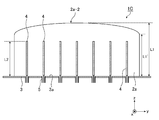
- the end 2a-2 of the conductor flat plate 2a of the antenna device 1C which is opposite to the surface 3a of the conductor short-circuit plate 3, is a curved side as shown in FIG.
- the length from the surface 3a along the normal direction (z direction) of the surface 3a to the end of the conductor plate 2a is the shortest at the side end in the y direction with the length L1 ', and goes to the center in the y direction.
- the center in the y direction is the longest at the length L1.
- the length L1 'of the side end of the conductive plate 2a is longer than the length L2 from the surface 3a along the z direction to the end of the tapered conductive plate 4.
- the y direction corresponds to the magnetic field direction of the antenna device 1C.
- L1 is the length of three quarters of the free space wavelength at the lower limit frequency of the operating frequency band of the antenna device 1.
- the beam width of the array element pattern increases.
- the antenna device 1C the beam width of the array element pattern is increased in the element antenna at the center in the y direction where the length from the surface 3a to the end of the conductor plate 2a is L1. Since the end side 2a-2 of the conductor plate 2a is a curved side, the antenna device 1C can be housed in a curved radome.
- the length of the curved side 2a-2 from the surface 3a along the z direction to the end of the conductive plate 2a is such that the minimum value of the gain within the coverage at each frequency of the operating frequency band is the largest. It has a curvature of a given length.
- the antenna device 1C becomes an antenna having a high minimum value of the gain in the coverage area over all frequencies of the operating frequency band.
- FIG. 11 is a diagram showing a configuration of an antenna device 1C ′ which is a modification of the antenna device 1C, and shows the antenna device 1C ′ as viewed in the ⁇ x direction.
- the description of the conductor flat plate 2a arranged in the + x direction among the pair of conductive flat plates 2a, 2a, which are the parallel flat plates 2, is omitted so that the tapered conductive plate 4 provided on the parallel flat plate 2 can be seen. ing.
- an end 2a-2 of the conductor flat plate 2a of the ’antenna device 1C ' which is opposite to the surface 3a of the conductor short-circuit plate 3, is an irregular side.
- the length from the surface 3a along the normal direction (z direction) of the surface 3a to the end of the conductor plate 2a is such that the side end in the y direction is the length L1 'and the center in the y direction is the length. L1.
- the length L1 'of the side end of the conductive plate 2a is longer than the length L2 from the surface 3a along the z direction to the end of the tapered conductive plate 4.
- the beam width of the array element pattern is increased in the element antenna at the center in the y direction where the length from the surface 3a to the end of the conductor plate 2a is L1.
- the uneven side 2a-2 has the largest length from the surface 3a along the z direction to the end of the conductor plate 2a, and the largest value of the gain within the coverage area at each frequency of the operating frequency band. It has an unevenness amount to be a length.
- the antenna device 1C By having the side 2a-2, the antenna device 1C 'becomes an antenna having a high minimum value of the gain in the coverage area over all frequencies of the operating frequency band.
- FIG. 12 is a diagram showing a configuration of an antenna device 1C "which is a modification of the antenna device 1C, and shows the antenna device 1C" viewed in the + y direction.
- each of the plurality of parallel flat plates 2 arranged along the normal direction (x direction) of the conductive flat plate 2 a is in the normal direction (z direction) of the surface 3 a of the conductive short circuit plate 3.
- From the surface 3a gradually changes along the arrangement direction (x direction) of the plurality of parallel flat plates 2.
- the x direction corresponds to the electric field direction of the antenna device 1C.
- the length from the surface 3a along the z direction to the end of the conductor plate 2a is equal to the length of the conductor plate 2a at the end in the x direction among the plurality of conductor plates 2a arranged in the x direction.
- L1 ' is the shortest, and the length of the conductor plate 2a gradually increases toward the center in the x direction.
- the length of the conductor plate 2a at the center in the x direction is the longest at L1.
- L1 ' is longer than the length L2 from the surface 3a along the z direction to the end of the tapered conductive plate 4.
- the antenna device 1C " since the length of the conductor flat plate 2a at the center in the x direction is L1, the beam width of the array element pattern in the element antenna at the center in the x direction is increased.
- a line connecting ends of the plurality of conductor flat plates 2a arranged in the x direction in the + z direction becomes a curved line when viewed from the y direction. This allows the antenna device 1C ′′ to be housed in a radome curved in the x direction.
- the end side of the conductor plate 2a is a curved side in the y direction
- the length of the plurality of conductor plate 2a arranged in the x direction is changed in the x direction.
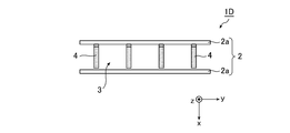
- FIG. 13 is a front view showing an element antenna array in an antenna device 1D according to the fourth embodiment.
- the element antenna includes a pair of conductor flat plates 2a, 2a, a parallel flat plate 2, a conductor short-circuiting plate 3, and one tapered conductive plate 4.
- a plurality of tapered conductive plates 4 are arranged one-dimensionally in the y direction on a pair of conductive flat plates 2a, 2a.
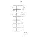
- FIG. 14 is a front view showing an element antenna array in an antenna device 1E which is a modification of the fourth embodiment.
- the element antenna includes a pair of conductor flat plates 2a, 2a, a parallel flat plate 2, a conductor short-circuit plate 3, and one tapered conductive plate 4.
- a plurality of parallel flat plates 2 each having one tapered conductive plate 4 are arranged one-dimensionally in the x direction.
- the length L1 from the surface 3a along the normal direction (z direction) of the surface 3a of the conductor short-circuit plate 3 to the end of the parallel flat plate 2 is the surface along the z direction. It is longer than the length L2 from 3a to the end of the tapered conductor plate 4a. L1 is the length of three quarters of the free space wavelength at the lower limit frequency of the operating frequency band.
- the same effect as that of the first embodiment can be obtained.
- the same effect as in the second embodiment can be obtained by partially or entirely filling the dielectric 9 between the pair of conductor flat plates 2a, 2a arranged in parallel with each other. Is obtained.
- the parallel plate 2 provided in the antenna device 1D has a structure in which L1 is changed along the antenna magnetic field direction, or the parallel plate 2 provided in the antenna device 1E has a structure in which L1 is changed in the antenna electric field direction. The same effect as in the third embodiment can be obtained.
- FIG. 15 is a front view showing an element antenna array in an antenna device 1F according to a modification of the fourth embodiment.
- the element antenna in the antenna device 1F, includes a pair of conductor flat plates 2a, 2a, a parallel flat plate 2, a conductor short-circuiting plate 3, and a single tapered conductive plate 4, and includes a plurality of conductive flat plates.
- the element antennas are arranged in a square. In the square arrangement, a plurality of element antennas form a square in which the adjacent conductor flat plates 2a, 2a and the adjacent tapered conductor plates 4, 4 form sides when viewed from the normal direction of the conductor short-circuit plate 3. Are arranged in a two-dimensional manner.
- FIG. 16 is a front view showing an element antenna array in an antenna device 1G according to a modification of the fourth embodiment.
- the element antenna in the antenna device 1 ⁇ / b> G, the element antenna includes a pair of conductor flat plates 2 a, a parallel flat plate 2, a conductor short-circuit plate 3, and a single tapered conductive plate 4.
- the element antennas are arranged aperiodically.
- the length L1 from the surface 3a along the normal direction (z direction) of the surface 3a of the conductor short-circuit plate 3 to the end of the parallel plate 2 is the surface along the z direction. It is longer than the length L2 from 3a to the end of the tapered conductor plate 4a. L1 is, for example, three-quarters of the free space wavelength at the lower limit frequency of the operating frequency band. In the antenna device 1F and the antenna device 1G having this configuration, the same effect as in the first embodiment can be obtained.
- the same effect as in the first embodiment can be obtained.
- the same effect as in the second embodiment can be obtained by partially or entirely filling the dielectric 9 between the pair of conductor flat plates 2a, 2a arranged in parallel with each other. Is obtained.
- the same effect as in the third embodiment can be obtained by forming the parallel plate 2 provided in the antenna device 1F into a structure in which L1 is changed in the antenna magnetic field direction or a structure in which L1 is changed in the antenna electric field direction.
- the antenna device can suppress radio wave leakage between element antennas straddling a parallel flat plate, so that the beam width of an array antenna can be widened, and can be used for radar or mobile communication equipment, for example. It is.
Landscapes
- Variable-Direction Aerials And Aerial Arrays (AREA)
- Waveguide Aerials (AREA)
Abstract
アンテナ装置(1)において、導体短絡板(3)の面(3a)の法線方向に沿った面(3a)から平行平板(2)の端部までの長さ(L1)が、面(3a)の法線方向に沿った面(3a)からテーパ状導体板(4)の端部までの長さ(L2)よりも長い。
Description
本発明は、アンテナ装置に関する。
超広帯域アンテナの一種として、テーパスロットアンテナ(Tapered Slot Antenna;以下、TSAと略して記載する)が知られている。例えば、特許文献1には、平行平板装荷TSAが記載されている。平行平板装荷TSAは、アンテナ開口を、送受信に使用される周波数帯域の上限周波数における半波長以下まで小型化しても容易に給電系との整合をとることができる。
超広帯域特性が必要なアレーアンテナとして平行平板装荷TSAを使用した場合、周波数帯域の低域側では、波長に換算したときの複数の素子アンテナ間の間隔が高域側よりも非常に狭くなる。このため、各々の素子アンテナが励振されたときに放射される電波が、平行平板を跨いで近接する他の素子アンテナに漏洩することがある。
前述した電波の漏洩が発生すると、近接する素子アンテナから電波の再放射が起こり、アレーアンテナを構成する複数の素子アンテナを各々1素子だけ励振したときに得られる放射パターン、すなわちアレー素子パターンのビーム幅が狭くなる。アレー素子パターンのビーム幅が狭くなると、アレーアンテナとしての覆域によっては、ビーム走査したときの利得低下が大きくなってしまうという課題があった。
本発明は上記課題を解決するものであり、アレーアンテナの素子アンテナとして用いた場合、平行平板を跨いだ素子アンテナ同士の電波の漏洩を抑圧することができるアンテナ装置を得ることを目的とする。
本発明に係るアンテナ装置は、互いに平行に配置された一対の導体平板である平行平板と、一対の導体平板の両方が電気的に接続された第1の面を有し、第1の面にて平行平板を短絡する導体短絡板と、一対の導体平板の間で、かつ、第1の面の法線方向と導体平板の法線方向とに平行な平面に沿って設けられ、導体平板の法線方向に導体幅が減少する形状を有したテーパ状導体板とを備え、第1の面の法線方向に沿った第1の面から平行平板の端部までの長さは、第1の面の法線方向に沿った第1の面からテーパ状導体板の端部までの長さよりも長いことを特徴とする。
本発明によれば、導体短絡板の第1の面の法線方向に沿った、第1の面から平行平板の端部までの長さは、第1の面の法線方向に沿った第1の面からテーパ状導体板の端部までの長さよりも長い。これにより、平行平板を跨いだ素子アンテナ同士の電波の漏洩を抑圧することができる。
実施の形態1.
図1は、実施の形態1に係るアンテナ装置1の構成を示す斜視図であり、アンテナ装置1がアレーアンテナである場合を示している。図2は、アンテナ装置1における素子アンテナ1aの構成を示す斜視図である。なお、以降では、アンテナ装置1がアレーアンテナである場合について説明するが、アンテナ装置1は、図2に示した素子アンテナ1a単体であってもよい。図1および図2において、平行平板2に設けられたテーパ状導体板4が見えるように、最上段の導体平板2aを透明に記載している。図3は、図1の+y方向に見たアンテナ装置1を示す図である。図4は、図1の-x方向に見たアンテナ装置1を示す図である。図4において、平行平板2に設けられたテーパ状導体板4が見えるように、平行平板2である一対の導体平板2a,2aのうち、+x方向に配置される導体平板2aの記載を省略している。図5は、図1の-z方向に見たアンテナ装置1を示す図である。
図1は、実施の形態1に係るアンテナ装置1の構成を示す斜視図であり、アンテナ装置1がアレーアンテナである場合を示している。図2は、アンテナ装置1における素子アンテナ1aの構成を示す斜視図である。なお、以降では、アンテナ装置1がアレーアンテナである場合について説明するが、アンテナ装置1は、図2に示した素子アンテナ1a単体であってもよい。図1および図2において、平行平板2に設けられたテーパ状導体板4が見えるように、最上段の導体平板2aを透明に記載している。図3は、図1の+y方向に見たアンテナ装置1を示す図である。図4は、図1の-x方向に見たアンテナ装置1を示す図である。図4において、平行平板2に設けられたテーパ状導体板4が見えるように、平行平板2である一対の導体平板2a,2aのうち、+x方向に配置される導体平板2aの記載を省略している。図5は、図1の-z方向に見たアンテナ装置1を示す図である。
図1において、アンテナ装置1は、複数の平行平板2、導体短絡板3および複数のテーパ状導体板4を備える。平行平板2は、互いに平行に配置された一対の導体平板2a,2aである。図1、図3、図4および図5において、各々が平行に配置された複数の導体平板2aのうち、隣接している導体平板2aと導体平板2aがいずれも平行平板2である。導体短絡板3は、接地電位とされた導体板部材であり、導体短絡板3の面3aは、一対の導体平板2a,2aの両方が電気的に接続される第1の面である。
テーパ状導体板4は、一対の導体平板2a,2aの間で、かつ、面3aの法線方向と導体平板2aの法線方向に平行な平面に沿って設けられ、導体平板2aの法線方向(x方向)に沿って導体幅が減少する形状を有している。図1から図5において、導体平板2aの平板面がy-z面に平行に設けられ、テーパ状導体板4の平板面がz-x面に平行に設けられ、アンテナ装置1における電波の主放射方向は、+z方向である。
なお、実施の形態1における法線方向は、面に直交した方向に加え、面に対する角度が面に直交した方向に近似され得る角度範囲の方向であってもよい。
なお、実施の形態1における法線方向は、面に直交した方向に加え、面に対する角度が面に直交した方向に近似され得る角度範囲の方向であってもよい。
平行平板2である一対の導体平板2a,2aのそれぞれの端面2a-1は、導体短絡板3の面3aに対向する端面である。端面2a-1は、図2に示すように面3aに電気的に接続されている。一対の導体平板2a,2aである平行平板2は、導体短絡板3の面3aにて短絡される。テーパ状導体板4の端面4-1は、導体平板2aの平板面に対向する端面である。端面4-1は、導体平板2aの平板面に電気的に接続されている。テーパ状導体板4は、同軸線路5における内部導体6によって給電され、導体短絡板3は、同軸線路5の外部導体7によって給電される。
図1、図2、図3および図4に示すように、導体短絡板3の面3aの法線方向(z方向)に沿った面3aから平行平板2の端部までの長さであるL1は、z方向に沿った面3aからテーパ状導体板4の端部までの長さであるL2よりも長い。L1は、アンテナ装置1の動作周波数帯域の下限周波数における自由空間波長の4分の1の奇数倍の長さである。以降の説明では、L1を、動作周波数帯域の下限周波数における自由空間波長の4分の3の長さであるものとする。
素子アンテナ1aは、図2に示すように、一対の導体平板2a,2a、一対の導体平板2a,2aの両方が電気的に接続された導体短絡板3、および一対の導体平板2a,2aの間に設けられた一枚のテーパ状導体板4を備えて構成されている。アンテナ装置1は、例えば、図5に示すように、複数の素子アンテナ1aが三角配列されたアレーアンテナである。三角配列は、例えば、図5に示した-x方向の最も端部にある平行平板2を1行目とし、これに+x方向に隣接する平行平板2を2行目とした場合に、奇数行に配列された平行平板2と偶数行に配列された平行平板2とで、隣接したテーパ状導体板4,4の間隔が半分ずつずれている配列である。なお、隣接したテーパ状導体板4,4がずれる大きさは、厳密にこれらの間隔の半分であってもよいが、半分と近似し得る範囲の大きさであればよい。
次に動作について説明する。
同軸線路5から給電された電波は、同軸線路5の内部導体6が接続されたテーパ状導体板4と、同軸線路5の外部導体7が接続された導体短絡板3との間で逆相で給電される。同軸線路5から給電された電波が、導体短絡板3とテーパ状導体板4との間で逆相で給電されることにより、導体短絡板3とテーパ状導体板4との間には電界が生じる。この電界は、導体短絡板3とテーパ状導体板4とで形成されるスロット線路から、テーパ状導体板4と平行平板2とで形成されるテーパスロット線路を伝搬して、平行平板2から自由空間に放射される。
同軸線路5から給電された電波は、同軸線路5の内部導体6が接続されたテーパ状導体板4と、同軸線路5の外部導体7が接続された導体短絡板3との間で逆相で給電される。同軸線路5から給電された電波が、導体短絡板3とテーパ状導体板4との間で逆相で給電されることにより、導体短絡板3とテーパ状導体板4との間には電界が生じる。この電界は、導体短絡板3とテーパ状導体板4とで形成されるスロット線路から、テーパ状導体板4と平行平板2とで形成されるテーパスロット線路を伝搬して、平行平板2から自由空間に放射される。
アンテナ装置1では、導体短絡板3の面3aの法線方向(z方向)に沿った面3aから平行平板2の端部までの長さL1が、z方向に沿った面3aからテーパ状導体板4の端部までの長さL2よりも長い。L1は、アンテナ装置1の動作周波数帯域の下限周波数における自由空間波長の4分の3の長さである。平行平板2の端部までの長さL1がテーパ状導体4の端部までの長さL2よりも高い位置にあるため、テーパ状導体板4の端部で反射される電波の一部は同軸線路5に戻らずに平行平板2に漏れ出し、良好な反射特性を維持することができる。
導体短絡板3に電気的に接続され、各々が平行に配置された複数の導体平板2a,2aは、図3に示すように溝の深さがL1であるコルゲート構造とみなすことができる。この構造において、L1は、例えば、自由空間波長の4分の3の長さであり、溝の底部である導体短絡板3は短絡され、溝の開口部では電界に対して開放されている。すなわち、溝に対して垂直な偏波、すなわち、x方向の偏波について高インピーダンス境界条件となり、溝の開口部表面は磁気壁となる。従って、溝の開口部表面ではx方向に進行する偏波成分の電波は伝搬しにくくなる。
従来の平行平板装荷TSAでは、自由空間を伝搬してきた電波が平行平板の配列方向(x方向)に近接した素子アンテナに伝搬した場合、アレーアンテナを構成する複数の素子アンテナをそれぞれ1素子だけ励振したときに得られる放射パターン、すなわち、アレー素子パターンのビーム幅が狭くなる。これに対し、アンテナ装置1では、自由空間を伝搬してきた電波がx方向に近接した素子アンテナに伝搬することが抑圧されるので、導体平板2aを跨いだ素子アンテナからの電波の再放射成分が抑えられる。このため、z-x面におけるアレー素子パターンのビーム幅が拡大される。
次に、アンテナ装置1の利点を説明するため、L1がL2よりも長く、L1が(3/4)λL(=0.75λL)であるアンテナ装置1のアレー素子パターンと、平行平板の長さがテーパ状導体板の長さと同一の0.47λLであるアンテナ装置(1)のアレー素子パターンとを比較する。ただし、λLは、動作周波数帯域の下限周波数における自由空間波長である。なお、平行平板の長さとは、平行平板である一対の導体平板の両方が電気的に接続された導体短絡板の面の法線方向に沿った上記面から平行平板の端部までの長さである。さらに、テーパ状導体板の長さは、平行平板である一対の導体平板の両方が電気的に接続された導体短絡板の面の法線方向に沿った上記面からテーパ状導体板の端部までの長さである。
アンテナ装置1として複数の素子アンテナ1aが三角配列されたアレーアンテナを想定する。複数の平行平板2が配列されたx方向のテーパ状導体板4の間隔L3が0.141λLであり、同一の平行平板2に配列されたテーパ状導体板4のy方向の間隔L4が0.155λLである。x方向は、アンテナ装置1の電界方向に相当し、y方向は、アンテナ装置1の磁界方向に相当する。
図6は、アレー素子パターンの全素子平均値を示すグラフである。図6に示すアレー素子パターンの全素子平均値は、アンテナ装置1とアンテナ装置(1)のz-x面におけるアレー素子パターンの全素子平均値である。アレー素子パターンの全素子平均値は、アレーアンテナが備える複数の素子アンテナを1つずつ給電したと仮定して算出される。図6のグラフにおける横軸はテーパ状導体板4がz軸からx軸になす角度を示しており、縦軸はアンテナ装置(1)のアレー素子パターンのボアサイト方向(z方向)のレベルで規格化された利得を示している。
破線の曲線(A)は、アンテナ装置(1)についてのz-x面のアレー素子パターンの全素子平均値である。実線の曲線(B)は、L1が(3/4)λL(=0.75λL)であるアンテナ装置1についてのz-x面のアレー素子パターンの全素子平均値を示している。両者を比較すると、アンテナ装置(1)よりもアンテナ装置1の方が、z-x面におけるアレー素子パターンのビーム幅が広い。これにより、アンテナ装置1では、アレーアンテナとしてビーム走査する場合に、ビーム走査における利得の低下を小さくすることが可能である。
次に、実施の形態1に係るアンテナ装置の変形例について説明する。
図7は、アンテナ装置1の変形例であるアンテナ装置1Aの構成を示す斜視図である。図7において、平行平板2に設けられたテーパ状導体板4が見えるように、最上段の導体平板2aを透明に記載している。また、図1と同一の構成要素には、同一の符号を付して説明を省略する。
図7は、アンテナ装置1の変形例であるアンテナ装置1Aの構成を示す斜視図である。図7において、平行平板2に設けられたテーパ状導体板4が見えるように、最上段の導体平板2aを透明に記載している。また、図1と同一の構成要素には、同一の符号を付して説明を省略する。
図7に示すように、アンテナ装置1Aにおいて、複数の平行平板2がx方向に沿って配列され、平行平板2である一対の導体平板2a,2aの間には、複数の誘電体基板8がy方向に沿って配列されている。複数の誘電体基板8は、導体平板2a,2aの間で、かつ導体短絡板3の法線方向と導体平板2aの法線方向とに平行な平面に沿って設けられる。
また、一つの誘電体基板8には、導体幅の減少する方向が逆である一対のテーパ状導体板4a,4aが形成されている。例えば、誘電体基板8には、図7に示す+x方向に導体幅が減少するテーパ状導体板4aと、-x方向に導体幅が減少するテーパ状導体板4aとが形成されている。なお、アンテナ装置1Aは、一対の導体平板2a,2aである平行平板2、導体短絡板3、および一対のテーパ状導体板4a,4aが形成された一枚の誘電体基板8を備えて構成された素子アンテナ単体であってもよい。
アンテナ装置1Aにおいても、導体短絡板3の面3aの法線方向(z方向)に沿った面3aから平行平板2の端部までの長さL1は、z方向に沿った面3aからテーパ状導体板4aの端部までの長さL2よりも長い。L1は、例えば、アンテナ装置1Aの動作周波数帯域の下限周波数における自由空間波長の4分の3の長さである。
この構成を有することにより、アンテナ装置1Aにおいて、テーパ状導体板4aの端部で反射される電波の一部は、同軸線路5に戻らず平行平板2に漏れ出すため、良好な反射特性を維持することができる。さらに、アンテナ装置1Aは、アンテナ装置1と同様に、溝の深さがL1であるコルゲート構造とみなせるので、z-x面におけるアレー素子パターンのビーム幅が拡大される。
また、導体短絡板3の面3aの法線方向(z方向)に沿った面3aから平行平板2の端部までの長さL1は、アンテナ装置1または1Aの動作周波数帯域の下限周波数における自由空間波長λLの4分の3の長さに限られず、自由空間波長λLの4分の1の奇数倍の長さであればよい。例えば、L1が(1/4)λLまたは(5/4)λLであっても、溝の底部で短絡され溝の開口部で電界に対して開放されたコルゲート構造とみなせるので、上記と同様の効果が得られる。
さらに、導体短絡板3の面3aの法線方向(z方向)に沿った面3aから平行平板2の端部までの長さL1は、アンテナ装置1または1Aの動作周波数帯域の特定の周波数における自由空間波長の4分の1の奇数倍の長さであってもよい。なお、特定の周波数とは、動作周波数帯域の下限周波数以外の周波数においてL1が自由空間波長の4分の1の奇数倍の長さとなる周波数である。このように構成されたアンテナ装置1または1Aでは、アレー素子パターンのビーム幅が広くなるので、ビーム走査するときの利得の低下を小さくすることができる。
z方向に沿った面3aから平行平板2の端部までの長さL1は、アンテナ装置1または1Aの動作周波数帯域の各々の周波数における、覆域内の利得の最小値が最も大きくなる長さである。例えば、L1が、アンテナ装置1または1Aの動作周波数帯域の特定の周波数における自由空間波長の4分の1の奇数倍の長さであると、アンテナ装置1または1Aの動作周波数帯域の各々の周波数における覆域内の利得の最小値は最も大きくなる。
以上のように、実施の形態1に係るアンテナ装置1または1Aにおいて、導体短絡板3の面3aの法線方向に沿った面3aから平行平板2の端部までの長さL1が、面3aの法線方向に沿った面3aからテーパ状導体板4または4aの端部までの長さL2よりも長い。このような構成を有することで、アンテナ装置1は、平行平板2を跨いだ素子アンテナ1a同士の電波の漏洩を抑圧することができる。
実施の形態1に係るアンテナ装置1において、平行平板2の長さL1は、動作周波数帯域の下限周波数における自由空間波長λLの4分の3の長さである。このように構成することにより、アレー素子パターンのビーム幅が広くなるので、ビーム走査するときの利得の低下を小さくすることができる。
実施の形態2.
実施の形態2では、実施の形態1と同様の効果が得られ、かつ、アレーアンテナとした場合に素子アンテナの高さを低くすることができるアンテナ装置について説明する。
図8は、実施の形態2に係るアンテナ装置1Bの構成を示す斜視図である。図8において、平行平板2に設けられたテーパ状導体板4が見えるように、最上段の導体平板2aと誘電体9を透明に記載している。図1と同一の構成要素には、同一の符号を付して説明を省略する。アンテナ装置1Bにおいて、互いに平行に配置された一対の導体平板2a,2aの間には、テーパ状導体板4が完全に埋まるまで全体的に誘電体9が充填されている。
実施の形態2では、実施の形態1と同様の効果が得られ、かつ、アレーアンテナとした場合に素子アンテナの高さを低くすることができるアンテナ装置について説明する。
図8は、実施の形態2に係るアンテナ装置1Bの構成を示す斜視図である。図8において、平行平板2に設けられたテーパ状導体板4が見えるように、最上段の導体平板2aと誘電体9を透明に記載している。図1と同一の構成要素には、同一の符号を付して説明を省略する。アンテナ装置1Bにおいて、互いに平行に配置された一対の導体平板2a,2aの間には、テーパ状導体板4が完全に埋まるまで全体的に誘電体9が充填されている。
アンテナ装置1Bにおいて、導体短絡板3の面3aの法線方向(z方向)に沿った面3aから平行平板2の端部までの長さL1は、z方向に沿った面3aからテーパ状導体板4aの端部までの長さL2よりも長い。L1は、アンテナ装置1Bの動作周波数帯域の各々の周波数における覆域内の利得の最小値が最も大きくなる長さであり、例えば、L1は、アンテナ装置1Bの動作周波数帯域の下限周波数における、誘電体9内の電波の伝搬波長の4分の1の奇数倍の長さである。
導体平板2a,2aの間を伝搬する電波は、導体平板2a,2aの間に充填された誘電体9によって波長が短縮される。一方、平行平板2の長さL1を、誘電体9における電波の波長の短縮分(1/√εr)だけ短くしても、実施の形態1と同様に、ビーム幅は拡大する。なお、εrは、誘電体9の比誘電率である。そこで、アンテナ装置1Bにおいて、L1がL2よりも長いという条件を維持しつつ、誘電体9によって電波の波長が短縮された分だけL1を短くすることで、アレーアンテナを構成する素子アンテナの高さを低くすることができる。
次に、実施の形態2に係るアンテナ装置の変形例について説明する。
図9は、アンテナ装置1Bの変形例である、アンテナ装置1B’の構成を示す斜視図である。図9において、平行平板2に設けられたテーパ状導体板4が見えるように、最上段の導体平板2aおよび誘電体9を透明に記載している。また、図8と同一の構成要素には同一の符号を付して説明を省略する。アンテナ装置1B’において、互いに平行に配置された一対の導体平板2a,2aの間には、テーパ状導体板4の一部が露出する程度に部分的に誘電体9が充填されている。
図9は、アンテナ装置1Bの変形例である、アンテナ装置1B’の構成を示す斜視図である。図9において、平行平板2に設けられたテーパ状導体板4が見えるように、最上段の導体平板2aおよび誘電体9を透明に記載している。また、図8と同一の構成要素には同一の符号を付して説明を省略する。アンテナ装置1B’において、互いに平行に配置された一対の導体平板2a,2aの間には、テーパ状導体板4の一部が露出する程度に部分的に誘電体9が充填されている。
アンテナ装置1B’においても、z方向に沿った面3aから平行平板2の端部までの長さL1は、z方向に沿った面3aからテーパ状導体板4aの端部までの長さL2よりも長い。L1は、アンテナ装置1B’の動作周波数帯域の各々の周波数における覆域内の利得の最小値が最も大きくなる長さであり、例えば、アンテナ装置1B’の動作周波数帯域の下限周波数における、誘電体9内の電波の伝搬波長の4分の1の奇数倍の長さである。
アンテナ装置1B’は、アンテナ装置1Bに比べて誘電体9の充填量が少ないが、一対の導体平板2a,2aの間を伝搬する電波は、誘電体9によって波長が短縮される。このため、誘電体9によって電波の波長が短縮された分だけL1を短くしても、実施の形態1と同様にビーム幅が拡大する。そこで、アンテナ装置1B’においても、L1がL2よりも長いという条件を維持しつつ、誘電体9によって電波の波長が短縮された分だけL1を短くすることで、アレーアンテナを構成する素子アンテナの高さを低くすることが可能である。
実施の形態3.
実施の形態3は、実施の形態1と同様の効果が得られ、かつ、レドームに収納することができるアンテナ装置について説明する。
図10は、実施の形態3に係るアンテナ装置1Cの構成を示す図であって、-x方向に見たアンテナ装置1Cを示している。図10において、平行平板2に設けられたテーパ状導体板4が見えるように、平行平板2である導体平板2a,2aのうち、+x方向に配置された導体平板2aの記載を省略している。
実施の形態3は、実施の形態1と同様の効果が得られ、かつ、レドームに収納することができるアンテナ装置について説明する。
図10は、実施の形態3に係るアンテナ装置1Cの構成を示す図であって、-x方向に見たアンテナ装置1Cを示している。図10において、平行平板2に設けられたテーパ状導体板4が見えるように、平行平板2である導体平板2a,2aのうち、+x方向に配置された導体平板2aの記載を省略している。
アンテナ装置1Cが備える導体平板2aにおける導体短絡板3の面3aとは反対側の端辺2a-2は、図10に示すように、曲線状の辺である。面3aの法線方向(z方向)に沿った面3aから導体平板2aの端部までの長さは、y方向の側端部が長さL1’で最も短く、y方向の中央部に向かうにつれて徐々に長くなり、y方向の中央部が長さL1で最も長い。ただし、導体平板2aの側端部の長さL1’は、z方向に沿った面3aからテーパ状導体板4の端部までの長さL2よりも長い。なお、y方向は、アンテナ装置1Cの磁界方向に相当する。
L1は、アンテナ装置1の動作周波数帯域の下限周波数における自由空間波長の4分の3の長さである。面3aから導体平板2aの端部までの長さがL1である素子アンテナでは、アレー素子パターンのビーム幅が拡大する。このため、アンテナ装置1Cでは、面3aから導体平板2aの端部までの長さがL1であるy方向の中央部の素子アンテナにおいて、アレー素子パターンのビーム幅が拡大する。導体平板2aの端辺2a-2が曲線状の辺であるので、アンテナ装置1Cを曲面状のレドームに収納することができる。
また、曲線状の端辺2a-2は、z方向に沿った面3aから導体平板2aの端部までの長さが、動作周波数帯域の各々の周波数における覆域内の利得の最小値が最も大きくなる長さとなる曲率を有する。この端辺2a-2を有することで、アンテナ装置1Cは、動作周波数帯域の全周波数に亘って覆域内の利得の最小値が高いアンテナとなる。
次に、実施の形態3に係るアンテナ装置の変形例について説明する。
図11はアンテナ装置1Cの変形例であるアンテナ装置1C’の構成を示す図であり、-x方向に見たアンテナ装置1C’を示している。図11において、平行平板2に設けられたテーパ状導体板4が見えるように、平行平板2である一対の導体平板2a,2aのうち、+x方向に配置された導体平板2aの記載を省略している。
図11はアンテナ装置1Cの変形例であるアンテナ装置1C’の構成を示す図であり、-x方向に見たアンテナ装置1C’を示している。図11において、平行平板2に設けられたテーパ状導体板4が見えるように、平行平板2である一対の導体平板2a,2aのうち、+x方向に配置された導体平板2aの記載を省略している。
アンテナ装置1C’が備える導体平板2aにおける導体短絡板3の面3aとは反対側の端辺2a-2は、図11に示すように、凹凸状の辺である。面3aの法線方向(z方向)に沿った面3aから導体平板2aの端部までの長さは、y方向の側端部が長さL1’であり、y方向の中央部が長さL1である。ただし、導体平板2aの側端部の長さL1’は、z方向に沿った面3aからテーパ状導体板4の端部までの長さL2よりも長い。アンテナ装置1C’では、面3aから導体平板2aの端部までの長さがL1であるy方向の中央部の素子アンテナにおいて、アレー素子パターンのビーム幅が拡大する。
また、凹凸状の端辺2a-2は、z方向に沿った面3aから導体平板2aの端部までの長さが、動作周波数帯域の各々の周波数における覆域内の利得の最小値が最も大きくなる長さとなる凹凸量を有する。この端辺2a-2を有することで、アンテナ装置1C’は、動作周波数帯域の全周波数に亘って覆域内の利得の最小値が高いアンテナとなる。
図12はアンテナ装置1Cの変形例であるアンテナ装置1C”の構成を示す図であり、+y方向に見たアンテナ装置1C”を示している。アンテナ装置1C”において、導体平板2aの法線方向(x方向)に沿って配列された複数の平行平板2のそれぞれの導体平板2aは、導体短絡板3の面3aの法線方向(z方向)に沿った面3aからの長さが複数の平行平板2の配列方向(x方向)に沿って徐々に変化している。x方向は、アンテナ装置1Cの電界方向に相当する。
例えば、z方向に沿った面3aから導体平板2aの端部までの長さは、x方向に配列された複数の導体平板2aのうち、x方向の端部にある導体平板2aの長さがL1’で最も短く、x方向の中央部に向かうにつれて導体平板2aの長さが徐々に長くなり、x方向の中央部にある導体平板2aの長さがL1で最も長い。ただし、L1’は、z方向に沿った面3aからテーパ状導体板4の端部までの長さL2よりも長い。
アンテナ装置1C”では、x方向の中央部にある導体平板2aの長さがL1であることから、x方向の中央部にある素子アンテナにおいてアレー素子パターンのビーム幅が拡大する。また、アンテナ装置1C”では、x方向に並んだ複数の導体平板2aの+z方向の端部を結んだ線が、y方向から見て曲線状の線になる。これにより、アンテナ装置1C”は、x方向に曲面状のレドームに収納することができる。
さらに、図11に示したように導体平板2aの端辺をy方向に曲線状の辺とし、図12に示したように、x方向に配列された複数の導体平板2aの長さをx方向に沿って曲線状に変化させたアンテナ装置であれば、y方向とx方向に曲面状のレドームに収納することが可能である。
実施の形態4.
実施の形態4では、三角配列以外の素子アンテナの配列について説明する。
図13は、実施の形態4に係るアンテナ装置1Dにおける素子アンテナ配列を示す正面図である。図13において、素子アンテナは、一対の導体平板2a,2aである平行平板2、導体短絡板3および一枚のテーパ状導体板4を備えて構成される。アンテナ装置1Dでは、一対の導体平板2a,2aにおいて複数のテーパ状導体板4がy方向に沿って一次元に配列されている。
実施の形態4では、三角配列以外の素子アンテナの配列について説明する。
図13は、実施の形態4に係るアンテナ装置1Dにおける素子アンテナ配列を示す正面図である。図13において、素子アンテナは、一対の導体平板2a,2aである平行平板2、導体短絡板3および一枚のテーパ状導体板4を備えて構成される。アンテナ装置1Dでは、一対の導体平板2a,2aにおいて複数のテーパ状導体板4がy方向に沿って一次元に配列されている。
図14は、実施の形態4の変形例であるアンテナ装置1Eにおける素子アンテナ配列を示す正面図である。図14において、素子アンテナは、一対の導体平板2a,2aである平行平板2、導体短絡板3および一枚のテーパ状導体板4を備えて構成される。アンテナ装置1Eは、一枚のテーパ状導体板4を有する複数の平行平板2が、x方向に沿って一次元に配列されている。
アンテナ装置1Dおよびアンテナ装置1Eにおいても、導体短絡板3の面3aの法線方向(z方向)に沿った面3aから平行平板2の端部までの長さL1は、z方向に沿った面3aからテーパ状導体板4aの端部までの長さL2よりも長い。L1は、動作周波数帯域の下限周波数における自由空間波長の4分の3の長さである。このように構成されたアンテナ装置1Dおよびアンテナ装置1Eにおいても実施の形態1と同様の効果が得られる。
また、アンテナ装置1Dまたはアンテナ装置1Eの素子アンテナが、図7に示した一対のテーパ状導体板4a,4aを備える構成であっても、実施の形態1と同様の効果が得られる。さらに、アンテナ装置1Dまたはアンテナ装置1Eにおいて、互いに平行に配置された一対の導体平板2a,2aの間に部分的または全体的に誘電体9を充填することで、実施の形態2と同様の効果が得られる。さらに、アンテナ装置1Dが備える平行平板2をアンテナ磁界方向に沿ってL1を変化させた構造、あるいは、アンテナ装置1Eが備える平行平板2をアンテナ電界方向にL1を変化させた構造にすることにより、実施の形態3と同様の効果が得られる。
図15は、実施の形態4の変形例であるアンテナ装置1Fにおける素子アンテナ配列を示す正面図である。図15に示すように、アンテナ装置1Fにおいて、素子アンテナは、一対の導体平板2a,2aである平行平板2、導体短絡板3および一枚のテーパ状導体板4を備えて構成され、複数の素子アンテナが四角配列されている。なお、四角配列では、導体短絡板3の法線方向から見て、複数の素子アンテナが、隣接した導体平板2a,2aと隣接したテーパ状導体板4,4がそれぞれ辺をなす四角形を形成するように二次元配列されている。
図16は、実施の形態4の変形例であるアンテナ装置1Gにおける素子アンテナ配列を示す正面図である。図16に示すように、アンテナ装置1Gにおいて、素子アンテナが、一対の導体平板2a,2aである平行平板2、導体短絡板3および一枚のテーパ状導体板4を備えて構成され、複数の素子アンテナが非周期配列されている。
アンテナ装置1Fおよびアンテナ装置1Gにおいても、導体短絡板3の面3aの法線方向(z方向)に沿った面3aから平行平板2の端部までの長さL1は、z方向に沿った面3aからテーパ状導体板4aの端部までの長さL2よりも長い。L1は、例えば、動作周波数帯域の下限周波数における自由空間波長の4分の3の長さである。この構成を有するアンテナ装置1Fおよびアンテナ装置1Gにおいても、実施の形態1と同様の効果が得られる。
また、アンテナ装置1Fまたはアンテナ装置1Gの素子アンテナが、図7に示したように一対のテーパ状導体板4a,4aを備える構成であっても、実施の形態1と同様の効果が得られる。さらに、アンテナ装置1Fまたはアンテナ装置1Gにおいて、互いに平行に配置された一対の導体平板2a,2aの間に部分的または全体的に誘電体9を充填することで、実施の形態2と同様の効果が得られる。さらに、アンテナ装置1Fが備える平行平板2を、アンテナ磁界方向にL1を変化させた構造、あるいはアンテナの電界方向にL1を変化させた構造にすることにより、実施の形態3と同様の効果が得られる。
なお、本発明は上記実施の形態に限定されるものではなく、本発明の範囲内において、実施の形態のそれぞれの自由な組み合わせまたは実施の形態のそれぞれの任意の構成要素の変形もしくは実施の形態のそれぞれにおいて任意の構成要素の省略が可能である。
本発明に係るアンテナ装置は、平行平板を跨いだ素子アンテナ同士の電波の漏洩を抑圧することができるので、アレーアンテナのビーム幅を広くすることができ、例えばレーダまたは移動体通信機器に利用可能である。
1,1A,1B,1B',1C,1C',1C”,1D,1E,1F,1G アンテナ装置、1a 素子アンテナ、2 平行平板、2a導体平板、2a-1,4-1 端面、2a-2 端辺、3 導体短絡板、3a 面、4,4a テーパ状導体板、5 同軸線路、6 内部導体、7 外部導体、8 誘電体基板、9 誘電体。
Claims (16)
- 互いに平行に配置された一対の導体平板である平行平板と、
前記一対の前記導体平板の両方が電気的に接続された第1の面を有し、前記第1の面にて前記平行平板を短絡する導体短絡板と、
前記一対の前記導体平板の間で、かつ、前記第1の面の法線方向と前記導体平板の法線方向とに平行な平面に沿って設けられ、前記導体平板の法線方向に沿って導体幅が減少する形状を有したテーパ状導体板とを備え、
前記第1の面の法線方向に沿った前記第1の面から前記平行平板の端部までの長さは、前記第1の面の法線方向に沿った前記第1の面から前記テーパ状導体板の端部までの長さよりも長いこと
を特徴とするアンテナ装置。 - 前記一対の前記導体平板の間に部分的または全体的に充填された誘電体を備えること
を特徴とする請求項1記載のアンテナ装置。 - 前記第1の面の法線方向に沿った前記第1の面から前記平行平板の端部までの長さは、動作周波数帯域の各々の周波数における覆域内の利得の最小値が最も大きくなる長さであること
を特徴とする請求項1記載のアンテナ装置。 - 前記第1の面の法線方向に沿った前記第1の面から前記平行平板の端部までの長さは、動作周波数帯域の特定の周波数における自由空間波長の4分の1の奇数倍の長さであること
を特徴とする請求項1記載のアンテナ装置。 - 前記第1の面の法線方向に沿った前記第1の面から前記平行平板の端部までの長さは、動作周波数帯域の下限周波数における自由空間波長の4分の1の奇数倍の長さであること
を特徴とする請求項1記載のアンテナ装置。 - 前記第1の面の法線方向に沿った前記第1の面から前記平行平板の端部までの長さは、動作周波数帯域の下限周波数における前記誘電体内の電波の伝搬波長の4分の1の奇数倍の長さであること
を特徴とする請求項2記載のアンテナ装置。 - 前記導体平板における前記第1の面とは反対側の端辺は、曲線状の辺であること
を特徴とする請求項1記載のアンテナ装置。 - 前記曲線状の辺は、前記第1の面の法線方向に沿った前記平行平板の前記第1の面からの長さが、動作周波数帯域の各々の周波数における覆域内の利得の最小値が最も大きくなる長さとなる曲率を有すること
を特徴とする請求項7記載のアンテナ装置。 - 前記導体平板における前記第1の面とは反対側の端辺は、凹凸状の辺であること
を特徴とする請求項1記載のアンテナ装置。 - 前記凹凸状の辺は、前記第1の面の法線方向に沿った前記平行平板の前記第1の面からの長さが、動作周波数帯域の各々の周波数における覆域内の利得の最小値が最も大きくなる長さとなる凹凸量を有すること
を特徴とする請求項9記載のアンテナ装置。 - 複数の前記平行平板が前記導体平板の法線方向に沿って配列されている場合、前記第1の面の法線方向に沿った前記第1の面から前記導体平板の端部までの長さは、複数の前記平行平板の配列方向に沿った端部から中央部に向けて徐々に長くなっていること
を特徴とする請求項1記載のアンテナ装置。 - 素子アンテナは、前記一対の前記導体平板である前記平行平板、前記導体短絡板および一枚の前記テーパ状導体板を備えて構成され、
複数の前記素子アンテナは、アンテナ電界方向またはアンテナ磁界方向に沿って配列されていること
を特徴とする請求項1記載のアンテナ装置。 - 素子アンテナは、前記一対の前記導体平板である前記平行平板、前記導体短絡板および一枚の前記テーパ状導体板を備えて構成され、
複数の前記素子アンテナは、二次元配列されていること
を特徴とする請求項1記載のアンテナ装置。 - 複数の前記素子アンテナは、四角配列されていること
を特徴とする請求項13記載のアンテナ装置。 - 複数の前記素子アンテナは、三角配列されていること
を特徴とする請求項13記載のアンテナ装置。 - 複数の前記素子アンテナは、非周期配列されていること
を特徴とする請求項13記載のアンテナ装置。
Priority Applications (2)
| Application Number | Priority Date | Filing Date | Title |
|---|---|---|---|
| PCT/JP2018/027488 WO2020021594A1 (ja) | 2018-07-23 | 2018-07-23 | アンテナ装置 |
| JP2020531840A JP6847313B2 (ja) | 2018-07-23 | 2018-07-23 | アンテナ装置 |
Applications Claiming Priority (1)
| Application Number | Priority Date | Filing Date | Title |
|---|---|---|---|
| PCT/JP2018/027488 WO2020021594A1 (ja) | 2018-07-23 | 2018-07-23 | アンテナ装置 |
Publications (1)
| Publication Number | Publication Date |
|---|---|
| WO2020021594A1 true WO2020021594A1 (ja) | 2020-01-30 |
Family
ID=69182308
Family Applications (1)
| Application Number | Title | Priority Date | Filing Date |
|---|---|---|---|
| PCT/JP2018/027488 Ceased WO2020021594A1 (ja) | 2018-07-23 | 2018-07-23 | アンテナ装置 |
Country Status (2)
| Country | Link |
|---|---|
| JP (1) | JP6847313B2 (ja) |
| WO (1) | WO2020021594A1 (ja) |
Cited By (1)
| Publication number | Priority date | Publication date | Assignee | Title |
|---|---|---|---|---|
| WO2022124168A1 (ja) * | 2020-12-10 | 2022-06-16 | 三菱電機株式会社 | アレーアンテナ装置 |
Citations (2)
| Publication number | Priority date | Publication date | Assignee | Title |
|---|---|---|---|---|
| JP2003152433A (ja) * | 2001-11-09 | 2003-05-23 | Mitsubishi Electric Corp | アンテナ装置 |
| JP2010251960A (ja) * | 2009-04-14 | 2010-11-04 | Mitsubishi Electric Corp | アンテナ装置 |
-
2018
- 2018-07-23 WO PCT/JP2018/027488 patent/WO2020021594A1/ja not_active Ceased
- 2018-07-23 JP JP2020531840A patent/JP6847313B2/ja active Active
Patent Citations (2)
| Publication number | Priority date | Publication date | Assignee | Title |
|---|---|---|---|---|
| JP2003152433A (ja) * | 2001-11-09 | 2003-05-23 | Mitsubishi Electric Corp | アンテナ装置 |
| JP2010251960A (ja) * | 2009-04-14 | 2010-11-04 | Mitsubishi Electric Corp | アンテナ装置 |
Cited By (3)
| Publication number | Priority date | Publication date | Assignee | Title |
|---|---|---|---|---|
| WO2022124168A1 (ja) * | 2020-12-10 | 2022-06-16 | 三菱電機株式会社 | アレーアンテナ装置 |
| JP7143551B1 (ja) * | 2020-12-10 | 2022-09-28 | 三菱電機株式会社 | アレーアンテナ装置 |
| EP4239795A4 (en) * | 2020-12-10 | 2024-06-12 | Mitsubishi Electric Corporation | Array antenna device |
Also Published As
| Publication number | Publication date |
|---|---|
| JPWO2020021594A1 (ja) | 2021-02-15 |
| JP6847313B2 (ja) | 2021-03-24 |
Similar Documents
| Publication | Publication Date | Title |
|---|---|---|
| JP6446547B2 (ja) | ワイヤレス電子デバイスのための周期スロットを有するストリップライン結合アンテナ | |
| US20160365647A1 (en) | Shared-aperture antenna and base station | |
| US20190288397A1 (en) | Microstrip antenna, antenna array and method of manufacturing microstrip antenna | |
| JP3923360B2 (ja) | スロットアレーアンテナ及びスロットアレーアンテナ装置 | |
| WO2015083457A1 (ja) | パッチアンテナ | |
| JP2015185946A (ja) | アンテナ装置 | |
| WO2015029946A1 (ja) | アンテナ及びセクタアンテナ | |
| US20140266957A1 (en) | Wide-angle antenna and array antenna | |
| US10601140B2 (en) | Electromagnetic wave radiator | |
| WO2022068548A1 (zh) | 后盖及终端 | |
| WO2020098441A1 (zh) | 一种周期性漏波天线 | |
| Patil et al. | Gain improvement of lower UWB monopole antenna using FSS layer | |
| EP3830903B1 (en) | Broadband antenna having polarization dependent output | |
| JP3810366B2 (ja) | ホーンアンテナ装置、およびこれを用いた方位探知用アンテナ装置 | |
| JP2014003436A (ja) | Ebg構造体を用いたアンテナ装置 | |
| JP2007059966A (ja) | アンテナおよびアレイアンテナ | |
| WO2020021594A1 (ja) | アンテナ装置 | |
| Giner et al. | Excitation of untilted narrow-wall slot in groove gap waveguide by using a parasitic dipole | |
| JP2010252172A (ja) | アンテナ装置 | |
| US20200185824A1 (en) | Antenna device | |
| JP5605285B2 (ja) | ダイポールアレーアンテナ | |
| US11817625B2 (en) | Electromagnetic wave radiator | |
| JP5520989B2 (ja) | アンテナおよび基地局アンテナ | |
| JP5822003B2 (ja) | セクタアンテナ | |
| JP6536950B2 (ja) | アンテナ装置 |
Legal Events
| Date | Code | Title | Description |
|---|---|---|---|
| 121 | Ep: the epo has been informed by wipo that ep was designated in this application |
Ref document number: 18928098 Country of ref document: EP Kind code of ref document: A1 |
|
| ENP | Entry into the national phase |
Ref document number: 2020531840 Country of ref document: JP Kind code of ref document: A |
|
| NENP | Non-entry into the national phase |
Ref country code: DE |
|
| 122 | Ep: pct application non-entry in european phase |
Ref document number: 18928098 Country of ref document: EP Kind code of ref document: A1 |