WO2020017322A1 - 入力装置 - Google Patents
入力装置 Download PDFInfo
- Publication number
- WO2020017322A1 WO2020017322A1 PCT/JP2019/026336 JP2019026336W WO2020017322A1 WO 2020017322 A1 WO2020017322 A1 WO 2020017322A1 JP 2019026336 W JP2019026336 W JP 2019026336W WO 2020017322 A1 WO2020017322 A1 WO 2020017322A1
- Authority
- WO
- WIPO (PCT)
- Prior art keywords
- resistance
- input device
- base material
- resistor
- portions
- Prior art date
- Legal status (The legal status is an assumption and is not a legal conclusion. Google has not performed a legal analysis and makes no representation as to the accuracy of the status listed.)
- Ceased
Links
Images


Classifications
-
- G—PHYSICS
- G06—COMPUTING OR CALCULATING; COUNTING
- G06F—ELECTRIC DIGITAL DATA PROCESSING
- G06F3/00—Input arrangements for transferring data to be processed into a form capable of being handled by the computer; Output arrangements for transferring data from processing unit to output unit, e.g. interface arrangements
- G06F3/01—Input arrangements or combined input and output arrangements for interaction between user and computer
- G06F3/03—Arrangements for converting the position or the displacement of a member into a coded form
- G06F3/041—Digitisers, e.g. for touch screens or touch pads, characterised by the transducing means
- G06F3/045—Digitisers, e.g. for touch screens or touch pads, characterised by the transducing means using resistive elements, e.g. a single continuous surface or two parallel surfaces put in contact
-
- G—PHYSICS
- G06—COMPUTING OR CALCULATING; COUNTING
- G06F—ELECTRIC DIGITAL DATA PROCESSING
- G06F2203/00—Indexing scheme relating to G06F3/00 - G06F3/048
- G06F2203/041—Indexing scheme relating to G06F3/041 - G06F3/045
- G06F2203/04102—Flexible digitiser, i.e. constructional details for allowing the whole digitising part of a device to be flexed or rolled like a sheet of paper
-
- H—ELECTRICITY
- H01—ELECTRIC ELEMENTS
- H01C—RESISTORS
- H01C1/00—Details
- H01C1/14—Terminals or tapping points or electrodes specially adapted for resistors; Arrangements of terminals or tapping points or electrodes on resistors
-
- H—ELECTRICITY
- H01—ELECTRIC ELEMENTS
- H01C—RESISTORS
- H01C1/00—Details
- H01C1/16—Resistor networks not otherwise provided for
-
- H—ELECTRICITY
- H10—SEMICONDUCTOR DEVICES; ELECTRIC SOLID-STATE DEVICES NOT OTHERWISE PROVIDED FOR
- H10F—INORGANIC SEMICONDUCTOR DEVICES SENSITIVE TO INFRARED RADIATION, LIGHT, ELECTROMAGNETIC RADIATION OF SHORTER WAVELENGTH OR CORPUSCULAR RADIATION
- H10F19/00—Integrated devices, or assemblies of multiple devices, comprising at least one photovoltaic cell covered by group H10F10/00, e.g. photovoltaic modules
- H10F19/30—Integrated devices, or assemblies of multiple devices, comprising at least one photovoltaic cell covered by group H10F10/00, e.g. photovoltaic modules comprising thin-film photovoltaic cells
Definitions
- the present invention relates to an input device.
- a touch panel mounted on a display device such as a liquid crystal display device for inputting information to an electronic device or the like is known.
- Touch panels are used for various purposes because they can be input based on information visually captured by a display device.
- a touch panel As such a touch panel, a resistive type and a capacitive type are widely known. Also, a magnetic touch panel having a switch matrix configuration has been proposed (for example, see Patent Document 1).
- any of the above-mentioned touch panels can obtain two-dimensional information in the XY directions and the like, but cannot obtain three-dimensional information including the Z directions.
- the present invention has been made in view of the above points, and has as its object to provide an input device capable of obtaining three-dimensional information.
- the input device may further include an insulating layer, a plurality of first resistance units arranged on one side of the insulating layer with the longitudinal direction facing the first direction, and the first resistor on the other side of the insulating layer.
- a plurality of second resistance portions juxtaposed in a second direction intersecting the one direction; a pair of electrodes provided at both ends of each of the first resistance portions and each of the second resistance portions; When the first resistance section and the second resistance section are pressed, the resistance between the pair of electrodes of the pressed first resistance section and the second resistance section is a magnitude of the pressing force. It changes continuously according to the degree.
- an input device that can obtain three-dimensional information can be provided.
- FIG. 2 is a plan view illustrating the input device according to the first embodiment. It is a sectional view (the 1) which illustrates the input device concerning a 1st embodiment.
- FIG. 2 is a cross-sectional view (part 2) illustrating the input device according to the first embodiment.
- FIG. 2 is a block diagram illustrating a touch panel according to the first embodiment.
- FIG. 2 is a block diagram illustrating a touch panel control device according to the first embodiment.
- FIG. 9 is a cross-sectional view illustrating an input device according to Modification Example 1 of the first embodiment.
- FIG. 9 is a cross-sectional view illustrating an input device according to a second modification of the first embodiment.
- FIG. 13 is a plan view illustrating an input device according to a third modification of the first embodiment.
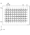
- FIG. 1 is a plan view illustrating the input device according to the first embodiment.
- FIG. 2 is a cross-sectional view illustrating the input device according to the first embodiment, and shows a cross section taken along line AA of FIG.
- the input device 1 includes a base material 10, a resistor 30 (a plurality of resistance units 31 and 32), and a plurality of terminal units 41 and 42.
- the side of the base material 10 on which the resistance portion 31 is provided is on the upper side or one side, and the side on which the resistance portion 32 is provided is on the lower side or the other side. Side.
- the surface on the side where the resistance portion 31 is provided is defined as one surface or upper surface, and the surface on the side where the resistance portion 32 is provided is defined as the other surface or lower surface.
- the input device 1 can be used upside down, or can be arranged at any angle.
- the plan view refers to viewing the target from the normal direction of the upper surface 10a of the base material 10
- the planar shape refers to the shape of the target viewed from the normal direction of the upper surface 10a of the base material 10.
- the base material 10 is an insulating member serving as a base layer for forming the resistor 30 and the like, and has flexibility.
- the thickness of the substrate 10 is not particularly limited and can be appropriately selected depending on the purpose. For example, the thickness can be about 5 ⁇ m to 500 ⁇ m. In particular, it is preferable that the thickness of the base material 10 be 5 ⁇ m to 200 ⁇ m, since the strain sensitivity error of the resistance portions 31 and 32 can be reduced.
- the substrate 10 is made of, for example, a PI (polyimide) resin, an epoxy resin, a PEEK (polyetheretherketone) resin, a PEN (polyethylene naphthalate) resin, a PET (polyethylene terephthalate) resin, a PPS (polyphenylene sulfide) resin, a polyolefin resin, or the like. From an insulating resin film.
- the film refers to a member having a thickness of about 500 ⁇ m or less and having flexibility.
- the base material 10 may be formed from, for example, an insulating resin film containing a filler such as silica or alumina.
- the base material 10 may be made of SiO 2 , ZrO 2 (including YSZ), Si, Si 2 N 3 , and Al 2 O 3 (including sapphire). , ZnO, perovskite ceramics (CaTiO 3 , BaTiO 3 ), and the like.
- the resistor 30 is formed on the base material 10 and is a sensing portion whose resistance value continuously changes according to the pressing force.
- the resistor 30 may be formed directly on the upper surface 10a and the lower surface 10b of the substrate 10, or may be formed on the upper surface 10a and the lower surface 10b of the substrate 10 via another layer.
- the resistor 30 includes a plurality of resistor portions 31 and 32 stacked with the base material 10 interposed therebetween. That is, the resistor 30 is a general term for the plurality of resistors 31 and 32, and is referred to as the resistor 30 unless it is necessary to particularly distinguish the resistors 31 and 32. In FIG. 1, for convenience, the resistance portions 31 and 32 are shown in a satin pattern.
- the plurality of resistance portions 31 are thin films that are juxtaposed in the Y direction at predetermined intervals on the upper surface 10a of the base material 10 with the longitudinal direction facing the X direction.
- the plurality of resistance portions 32 are thin films that are juxtaposed in the X direction at predetermined intervals on the lower surface 10b of the base material 10 with the longitudinal direction facing the Y direction.
- the plurality of resistance portions 31 and the plurality of resistance portions 32 do not need to be orthogonal to each other in a plan view, but may intersect.
- the resistor 30 can be formed from, for example, a material containing Cr (chromium), a material containing Ni (nickel), or a material containing both Cr and Ni. That is, the resistor 30 can be formed from a material containing at least one of Cr and Ni.
- a material containing Cr for example, a Cr mixed-phase film is given.
- the material containing Ni include, for example, Cu—Ni (copper nickel).
- Ni—Cr nickel chrome
- the Cr mixed phase film is a film in which Cr, CrN, Cr 2 N, and the like are mixed.
- the Cr mixed phase film may contain unavoidable impurities such as chromium oxide.
- the thickness of the resistor 30 is not particularly limited and can be appropriately selected depending on the purpose.
- the thickness can be about 0.05 ⁇ m to 2 ⁇ m.
- the thickness of the resistor 30 be 0.1 ⁇ m or more, since the crystallinity of the crystal constituting the resistor 30 (for example, the crystallinity of ⁇ -Cr) is improved.
- the thickness of the resistor 30 be 1 ⁇ m or less in that cracks in the film and warpage from the substrate 10 due to internal stress of the film constituting the resistor 30 can be reduced.
- the width of the resistor 30 is not particularly limited and can be appropriately selected depending on the purpose.
- the width can be about 0.1 ⁇ m to 1000 ⁇ m (1 mm).
- the pitch between the adjacent resistors 30 is not particularly limited and can be appropriately selected according to the purpose.
- the pitch can be about 1 mm to 100 mm.
- FIG. 1 and FIG. 2 show six resistance parts 31 and ten resistance parts 32, the resistance parts 31 and 32 are actually provided in the order of several hundreds to several 10,000s.
- the temperature coefficient of the resistor 30 can be stabilized by using ⁇ -Cr (alpha chromium), which is a stable crystal phase, as a main component, and the resistor 30 can withstand a pressing force.
- ⁇ -Cr alpha chromium
- the main component means that the target substance occupies 50% by mass or more of all the substances constituting the resistor.
- the main component stabilizes the temperature coefficient of the resistor 30 and the sensitivity of the resistor 30 to the pressing force.
- the resistor 30 preferably contains ⁇ -Cr in an amount of 80% by weight or more. Note that ⁇ -Cr is Cr having a bcc structure (body-centered cubic lattice structure).
- the terminal portions 41 extend from both ends of each of the resistance portions 31 on the upper surface 10a of the base material 10, and are formed in a substantially rectangular shape so as to be wider than the resistance portions 31 in plan view.
- the terminal portion 41 is a pair of electrodes for outputting a change in the resistance value of the resistance portion 31 caused by the pressing force to the outside.
- a flexible substrate or a lead wire for external connection is joined.
- the upper surface of the terminal portion 41 may be covered with a metal having better solderability than the terminal portion 41.
- the resistance part 31 and the terminal part 41 are shown with different symbols for convenience, they can be integrally formed of the same material in the same step.
- the terminal portions 42 extend from both ends of each of the resistor portions 32 on the lower surface 10b of the base material 10, and are formed in a substantially rectangular shape so as to be wider than the resistor portions 32 in a plan view.
- the terminal section 42 is a pair of electrodes for outputting a change in the resistance value of the resistance section 32 caused by the pressing force to the outside, and is connected to, for example, a flexible board or a lead wire for external connection.
- the upper surface of the terminal portion 42 may be covered with a metal having better solderability than the terminal portion 42.
- the resistance part 32 and the terminal part 42 are shown with different symbols for convenience, they can be integrally formed of the same material in the same step.
- a through wiring (through hole) penetrating the base material 10 may be provided, and the terminal portions 41 and 42 may be integrated on the upper surface 10a side or the lower surface 10b side of the base material 10.
- a cover layer may be provided on the upper surface 10a of the base material 10 so as to cover the resistance portion 31 and expose the terminal portion 41. Further, a cover layer (insulating resin layer) may be provided on the lower surface 10b of the base material 10 so as to cover the resistance portion 32 and expose the terminal portion 42.
- the cover layer By providing the cover layer, it is possible to prevent mechanical damage or the like from occurring in the resistance portions 31 and 32. By providing the cover layer, the resistance portions 31 and 32 can be protected from moisture and the like. Note that the cover layer may be provided so as to cover the entire portion except for the terminal portions 41 and 42.
- the cover layer can be formed from an insulating resin such as a PI resin, an epoxy resin, a PEEK resin, a PEN resin, a PET resin, a PPS resin, and a composite resin (for example, a silicone resin or a polyolefin resin).
- the cover layer may contain a filler or a pigment.
- the thickness of the cover layer is not particularly limited and can be appropriately selected depending on the purpose. For example, the thickness can be about 2 ⁇ m to 30 ⁇ m.
- the base material 10 is prepared, and the planar resistive part 31 and the terminal part 41 shown in FIG. 1 are formed on the upper surface 10 a of the base material 10.
- the materials and thicknesses of the resistance portion 31 and the terminal portion 41 are as described above.
- the resistance section 31 and the terminal section 41 can be integrally formed of the same material.
- the resistance portion 31 and the terminal portion 41 can be formed by, for example, forming a film by a magnetron sputtering method using a material capable of forming the resistance portion 31 and the terminal portion 41 as a target, and patterning the film by photolithography.
- the resistance section 31 and the terminal section 41 may be formed by a reactive sputtering method, an evaporation method, an arc ion plating method, a pulse laser deposition method, or the like instead of the magnetron sputtering method.
- the film thickness of the underlayer is 1 nm to 100 nm. It is preferable to form a functional layer with a degree of vacuum deposition.
- the functional layer can be formed, for example, by a conventional sputtering method.
- the functional layer is patterned by photolithography together with the resistance part 31 and the terminal part 41 into the planar shape shown in FIG.
- the functional layer refers to a layer having a function of promoting crystal growth of at least the upper resistive portion.
- the functional layer preferably further has a function of preventing oxidation of the resistance portion by oxygen or moisture contained in the base material 10 and a function of improving adhesion between the base material 10 and the resistance portion.
- the functional layer may further have another function.
- the insulating resin film constituting the base material 10 contains oxygen and moisture, especially when the resistance portion contains Cr, Cr forms a self-oxidized film, so that the functional layer has a function of preventing oxidation of the resistance portion. Is valid.
- the material of the functional layer is not particularly limited and may be appropriately selected depending on the purpose as long as it has a function of promoting the crystal growth of at least the upper resistive portion.
- the material include Cr (chromium) and Ti (titanium). ), V (vanadium), Nb (niobium), Ta (tantalum), Ni (nickel), Y (yttrium), Zr (zirconium), Hf (hafnium), Si (silicon), C (carbon), Zn (zinc) ), Cu (copper), Bi (bismuth), Fe (iron), Mo (molybdenum), W (tungsten), Ru (ruthenium), Rh (rhodium), Re (rhenium), Os (osmium), Ir (iridium) ), Pt (platinum), Pd (palladium), Ag (silver), Au (gold), Co (cobalt), Mn (manganese), Al (aluminum) One or more metals, or metal alloys of this group, or
- Examples of the above alloy include FeCr, TiAl, FeNi, NiCr, CrCu and the like.
- Examples of the above compounds include TiN, TaN, Si 3 N 4 , TiO 2 , Ta 2 O 5 , and SiO 2 .
- the functional layer can be formed, for example, by a conventional sputtering method using a material capable of forming the functional layer as a target and introducing an Ar (argon) gas into the chamber.
- Ar argon
- the functional layer is formed while the upper surface 10a of the substrate 10 is etched with Ar, so that the effect of improving the adhesion can be obtained by minimizing the amount of the functional layer formed.
- the functional layer may be formed by another method.
- the upper surface 10a of the base material 10 is activated by plasma treatment using Ar or the like to obtain an adhesion improving effect, and thereafter, the functional layer is formed into a vacuum by a magnetron sputtering method. May be used.
- the combination of the material of the functional layer and the material of the resistor portion 31 and the terminal portion 41 is not particularly limited and can be appropriately selected depending on the purpose.
- the resistance section 31 and the terminal section 41 can be formed by a magnetron sputtering method using a raw material capable of forming a Cr mixed phase film as a target and introducing Ar gas into the chamber.
- the resistive portion 31 and the terminal portion 41 may be formed by reactive sputtering using a target of pure Cr and an appropriate amount of nitrogen gas together with Ar gas.
- the growth surface of the Cr mixed phase film is defined by the function layer made of Ti as a trigger, and a Cr mixed phase film having ⁇ -Cr as a main component, which has a stable crystal structure, can be formed. Further, by diffusing Ti constituting the functional layer into the Cr mixed phase film, it is possible to stabilize the temperature coefficient of the resistance portion 31 and to improve the sensitivity of the resistance portion 31 to the pressing force.
- the Cr mixed phase film may include Ti or TiN (titanium nitride).
- the functional layer made of Ti has a function of promoting crystal growth of the resistance part 31 and a function of preventing oxidation of the resistance part 31 by oxygen or moisture contained in the base material 10. And all the functions of improving the adhesion between the base material 10 and the resistance portion 31.
- Ta, Si, Al, or Fe is used instead of Ti as the functional layer.
- the input device 1 by providing the functional layer below the resistor 31, the crystal growth of the resistor 31 can be promoted, and the resistor 31 having a stable crystal phase can be manufactured. As a result, in the input device 1, it is possible to realize stabilization of the temperature coefficient of the resistance unit 31 and improvement of the sensitivity of the resistance unit 31 to the pressing force. In addition, by diffusing the material forming the functional layer into the resistance portion 31, the input device 1 can realize stabilization of the temperature coefficient of the resistance portion 31 and improvement in sensitivity of the resistance portion 31 to a pressing force. .
- the resistance part 32 and the terminal part 42 having a planar shape shown in FIG. 1 are formed.
- the resistance part 32 and the terminal part 42 can be formed in the same manner as the resistance part 31 and the terminal part 41.
- a cover layer that covers the resistance part 31 on the upper surface 10 a of the base material 10 and exposes the terminal part 41 may be formed on the base material 10.
- a cover layer that covers the resistance portion 32 and exposes the terminal portion 42 may be provided on the lower surface 10b.
- the cover layer is formed, for example, by laminating a thermosetting insulating resin film in a semi-cured state so as to cover the resistance portion 31 on the upper surface 10a of the base material 10 and expose the terminal portion 41, and then heat and cure the film. be able to.
- the cover layer may be formed, for example, by laminating a thermosetting insulating resin film in a semi-cured state so as to cover the resistance portion 32 on the lower surface 10b of the base material 10 and expose the terminal portion 42, and then cure by heating. Can be made.
- the cover layer may be formed by applying a liquid or paste-like thermosetting insulating resin and heating and curing the resin.
- the input device 1 has the cross-sectional shape shown in FIG. Layers indicated by reference numerals 20a and 20b are functional layers.
- the planar shape of the input device 1 provided with the functional layers 20a and 20b is the same as that in FIG.
- the touch panel 3 can be realized by the input device 1 and the control device 2.
- the touch panel 3 is a panel on which an input operation can be performed by touching with a pen or a finger.
- the touch panel 3 is mounted on a front surface or a rear surface of the display device, and can be widely used for various electronic devices such as a personal computer and a smartphone, a portable terminal, and the like.
- Examples of a display device on which the touch panel 3 is mounted include, but are not limited to, a liquid crystal display device and an organic EL (Electro-Luminescence) display device.
- the input device 1 may be mounted on the display device such that the resistance portion 31 is on the display device side, or is mounted on the display device such that the resistance portion 32 is on the display device side. May be done.
- each of the terminal portions 41 and 42 of the input device 1 is connected to the control device 2 using, for example, a flexible substrate or a lead wire.
- the control device 2 can detect the coordinates of the position where the input device 1 is pressed and the magnitude of the pressing force based on the information obtained via the terminals 41 and 42 of the input device 1.
- the resistor 31 of the input device 1 can be used for detecting the X coordinate
- the resistor 32 can be used for detecting the Y coordinate.
- control device 2 can be configured to include, for example, an analog front end unit 21 and a signal processing unit 22.
- the analog front end unit 21 includes, for example, an input signal selection switch, a bridge circuit, an amplifier, an analog / digital conversion circuit (A / D conversion circuit), and the like.
- the analog front end unit 21 may include a temperature compensation circuit.
- all the terminal units 41 and 42 of the input device 1 are connected to an input signal selection switch, and a pair of electrodes is selected by the input signal selection switch.
- the pair of electrodes selected by the input signal selection switch is connected to a bridge circuit.
- one side of the bridge circuit is formed of a resistor between a pair of electrodes selected by the input signal selection switch, and the other three sides are formed of fixed resistors.
- a voltage (analog signal) corresponding to the resistance value of the resistor between the pair of electrodes selected by the input signal selection switch can be obtained as the output of the bridge circuit.
- the input signal selection switch is configured to be controllable by the signal processing unit 22.
- the voltage output from the bridge circuit is amplified by an amplifier, converted to a digital signal by an A / D conversion circuit, and sent to the signal processing unit 22.
- the analog front end unit 21 has a temperature compensation circuit, a digital signal whose temperature has been compensated is sent to the signal processing unit 22.
- a digital signal corresponding to the resistance values of all the terminal units 41 and 42 of the input device 1 can be sent to the signal processing unit 22 in a very short time.
- the signal processing unit 22 can detect the coordinates of the position where the input device 1 is pressed and the magnitude of the pressing force based on the information sent from the analog front end unit 21. For example, when the resistance value of the resistor portion 31 located at the bottom of FIG. 1 and the resistance value of the resistor portion 32 located second from the left change, it is determined that the portion B shown in FIG. Can be detected. Further, based on the magnitude of the change in the resistance value of the lowermost resistor portion 31 and the magnitude of the change in the resistance value of the resistor portion 32 located second from the left, the pressing force at the portion B shown in FIG. Can be detected.
- the magnitude of the pressing force is small, for example, only the resistance portion closer to the pressed side of the resistance portions 31 and 32 is pressed, and the resistance portion farther from the pressed side is It may not be pressed. In this case, only the resistance value between the pair of electrodes of the resistance portion closer to the pressed side changes continuously according to the magnitude of the pressing force, but also in this case, the signal processing unit 22 The magnitude of the pressing force can be detected based on the magnitude of the change in the resistance value of the resistance portion closer to the pressed side.
- the resistance value between the pair of electrodes of the pressed resistance part depends on the magnitude of the pressing force. Change continuously. Then, regardless of whether one of the resistance unit 31 and the resistance unit 32 is pressed or both are pressed, the signal processing unit 22 determines the magnitude of the pressing force based on the magnitude of the change in the resistance value of the pressed resistance unit. Can be detected.
- the signal processing unit 22 can be configured to include, for example, a CPU (Central Processing Unit), a ROM (Read Only Memory), a RAM (Random Access Memory), a main memory, and the like.
- a CPU Central Processing Unit
- ROM Read Only Memory
- RAM Random Access Memory
- various functions of the signal processing unit 22 can be realized by reading a program recorded in a ROM or the like into the main memory and executing the program by the CPU.
- part or all of the signal processing unit 22 may be realized only by hardware.
- the signal processing unit 22 may be physically configured by a plurality of devices or the like.
- the input device 1 can obtain three-dimensional information (the coordinates of the pressed position and the magnitude of the pressing force).
- the three-dimensional information obtained by the input device 1 is sent to the control device 2, and based on the three-dimensional information obtained by the input device 1, the control device 2 determines the coordinates of the position where the input device 1 is pressed. At the same time, the magnitude of the pressing force can be detected.
- the sensitivity of the resistance value to the pressing force (the same as when the resistance portions 31 and 32 are formed from Cu—Ni or Ni—Cr) is the same. (The amount of change in the resistance value of the resistance portions 31 and 32 with respect to the pressing force).
- the sensitivity of the resistance value to the pressing force is about 5 to less than when the resistance portions 31 and 32 are formed of Cu—Ni or Ni—Cr. It becomes about 10 times. Therefore, by forming the resistance portions 31 and 32 from the Cr mixed phase film, the detection accuracy of the coordinates of the pressed position can be improved, and the pressing force can be detected with high sensitivity.
- a predetermined operation is performed when it is detected that the pressing force is small, and another operation is performed when it is detected that the pressing force is medium. Then, when it is detected that the pressing force is large, it is possible to realize control for performing another operation. Alternatively, it is possible to realize a control in which the operation is not performed when the pressing force is detected to be small or medium, and the predetermined operation is performed only when the pressing force is detected to be large. This can prevent a malfunction due to a mistouch.
- the touch panel 3 is mounted on the back side of the display device, and even when the touch panel 3 is pressed via the display device, the presence or absence of the pressing and the magnitude of the pressing force can be detected. . Therefore, the touch panel 3 is mounted on the back side of the display device, and input to the touch panel 3 can be performed without lowering the visibility of the display device.
- the width of the resistance portions 31 and 32 (for example, to 10 ⁇ m or less), it is possible to suppress a decrease in the visibility of the display device, so that the touch panel 3 can be mounted on the front side of the display device. is there.
- FIG. 6 is a cross-sectional view illustrating an input device according to Modification Example 1 of the first embodiment, and shows a cross section corresponding to FIG.
- input device 1A is different from input device 1 (see FIGS. 1 and 2) in that electronic component 200 is mounted on lower surface 10b of base material 10.
- the electronic component 200 is, for example, an IC in which the analog front-end unit 21 shown in FIG. 5 has an IC and has an external communication function (for example, a serial communication function such as I 2 C). That is, the electronic component 200 is, for example, an IC having an input signal selection switch, a bridge circuit, an amplifier, an A / D conversion circuit, an external communication function, and the like, and has a resistance value between a pair of electrodes of the resistance units 31 and 32. Can be converted to a voltage and output as a digital signal.
- the electronic component 200 may include a temperature compensation circuit.
- the electronic component 200 can transmit and receive information to and from the signal processing unit 22 of the control device 2 by an external communication function.
- the electronic component 200 can be flip-chip mounted on, for example, a pad formed on the lower surface 10b of the base material 10.
- the electronic component 200 may be mounted on the lower surface 10 b of the substrate 10 via an adhesive layer such as a die attach film, and may be wire-bonded to a pad formed on the lower surface 10 b of the substrate 10.
- a passive component such as a capacitor may be mounted together with the electronic component 200.
- the electronic component 200 is connected to all the terminal portions 41 and 42 via a wiring pattern (not shown) and a through wiring (through hole).
- the electronic component 200 is configured to be able to supply power from outside the input device 1A.
- a cover layer may be provided on the upper surface 10a of the base material 10 so as to cover the resistance section 31 and the terminal section 41. Further, a cover layer (insulating resin layer) may be provided on the lower surface 10b of the base material 10 so as to cover the resistance part 32, the terminal part 42, and the electronic component 200.
- the cover layer By providing the cover layer, it is possible to prevent mechanical damage or the like from occurring in the resistance portions 31 and 32, the terminal portions 41 and 42, and the electronic component 200. Further, by providing the cover layer, the resistance portions 31 and 32, the terminal portions 41 and 42, and the electronic component 200 can be protected from moisture and the like.
- the terminal portions 41 and 42 and the electronic component 200 are short-distance via the wiring pattern or the through wiring (through hole). Connectable. Therefore, a small input device 1A can be realized.
- This structure is particularly effective for a small-sized input device in which it is difficult to connect a resistor and an electronic component with a lead wire using solder or the like.
- FIG. 6 illustrates an example in which the electronic component 200 is mounted on the lower surface 10 b of the base 10, but the electronic component 200 may be mounted on the upper surface 10 a of the base 10.
- the electronic component 200 is not limited to an IC having the function of the analog front end unit 21, and may be, for example, an IC having the functions of the analog front end unit 21 and the signal processing unit 22.
- a part or all of the control device 2 may be integrated with the input device 1A.
- integrating with the input device 1A means that a part or all of the base material and electronic components used for the control device 2 and a part or all of the base material and electronic components used for the input device 1A are combined. Including being shared.
- Modification 2 of the first embodiment an example of an input device having a solar cell mounted on one surface side or the other surface side of a base material will be described.
- the description of the same components as those of the embodiment described above may be omitted.
- FIG. 7 is a cross-sectional view illustrating an input device according to Modification 2 of the first embodiment, and shows a cross section corresponding to FIG. Referring to FIG. 7, input device 1B is different from input device 1A (see FIG. 6) in that solar cell 300 is mounted.
- the solar cell 300 is mounted on the lower surface 10b side of the base material 10.
- cover layer 60 is provided on lower surface 10 b of base material 10 so as to cover resistance portion 32, terminal portion 42, and electronic component 200, and solar cell 300 is disposed on the lower surface of cover layer 60.
- the solar cell 300 is connected to the electronic component 200 via a wiring pattern (not shown) or a through wiring (through hole), and can supply power to the electronic component 200.
- the solar cell 300 is obtained by laminating an amorphous silicon-based, silicon crystal-based, or compound-based (for example, CIGS) flexible solar cell on the cover layer 60, for example.
- CIGS is a compound solar cell containing copper (Cu), indium (In), gallium (Ga), and selenium (Se) as main components.
- the solar cell 300 which is a power supply for supplying power to the electronic component 200, is mounted.
- a small-sized input device 1B that does not require external power supply can be realized.
- the resistance of the resistor 30 is about 1 k ⁇ .
- the resistance value of the resistor 30 can be made 5 k ⁇ or more. Therefore, when a Cr mixed phase film is used as the material of the resistor 30, the current flowing through the resistor 30 is reduced, and power consumption can be reduced. Further, since the current supplied from the solar cell 300 can be reduced by reducing power consumption, a small-sized solar cell 300 can be used, and the entire input device 1B can be reduced in size.
- FIG. 7 shows an example in which the solar cell 300 is mounted on the lower surface 10b of the substrate 10, but the solar cell 300 may be mounted on the upper surface 10a of the substrate 10.
- the solar cell 300 is directly provided on the upper surface 10a of the base material 10 where the resistance portion 31 is not formed, or on the lower surface 10b of the base material 10 where the resistance portion 32 is not formed without using a cover layer. May be implemented.
- a solar cell 300 instead of a method of laminating a flexible solar cell, a solar cell in which a first electrode layer, a power generation layer, a second electrode layer, and the like are sequentially stacked on a cover layer or the like by, for example, vapor deposition or sputtering.
- a battery may be manufactured.
- a small battery (such as a lithium ion battery) may be used instead of the solar cell 300 as the power supply.
- a third modification of the first embodiment an example is shown in which the resistance section of the input device is formed in a zigzag pattern.
- the description of the same components as those of the embodiment described above may be omitted.
- FIG. 8 is a plan view illustrating an input device according to Modification 3 of the first embodiment, and shows a plane corresponding to FIG.
- input device 1C differs from input device 1 (see FIGS. 1 and 2) in that resistor 30 is replaced with resistor 30C.
- the resistor 30C includes the resistor portions 31C and 32C.
- the resistance portion 31C is a zigzag pattern formed between the pair of terminal portions 41.
- the resistance portion 32C is a zigzag pattern formed between the pair of terminal portions 42.
- the material and thickness of the resistance portions 31C and 32C can be the same as the material and thickness of the resistance portions 31 and 32, for example.
- the resistance value between the pair of terminal portions 41 and the resistance value between the pair of terminal portions 42 are reduced as compared with the case of forming a linear pattern. Can be higher.
- the amount of change in the resistance value between the pair of terminal portions 41 and the amount of change in the resistance value between the pair of terminal portions 42 when pressed are increased, so that the detection accuracy of the coordinates of the pressed position is improved.
- the pressure can be further improved and the pressing force can be detected with higher sensitivity.
- the resistance portion 31 is provided on the upper surface 10a of the base material 10 as the insulating layer and the resistance portion 32 is provided on the lower surface 10b has been described, but the resistance portion 32 is provided on one side of the insulating layer.
- the present invention is not limited to this, as long as the resistor portion 32 is provided on the other side.
- the resistance part 31 may be provided on the upper surface 10a of the base material 10
- the insulating layer covering the resistance part 31 may be provided on the upper surface 10a of the base material 10
- the resistance part 32 may be provided on the insulating layer.
- a first base material provided with the resistance part 31 and a second base material provided with the resistance part 32 are manufactured, and the resistance part 31 and the resistance part 32 are directed inward, and the resistance part 31 is sandwiched with an insulating layer therebetween.
- the provided first base material and the second base material provided with the resistance portion 32 may be bonded together.
- a first base material provided with the resistance part 31 and a second base material provided with the resistance part 32 are produced, and the first base material provided with the resistance part 31 and the second base material provided with the resistance part 32 are prepared. They may be stacked in the same direction. The same applies to the input devices 1A, 1B, and 1C.
Landscapes
- Engineering & Computer Science (AREA)
- General Engineering & Computer Science (AREA)
- Theoretical Computer Science (AREA)
- Microelectronics & Electronic Packaging (AREA)
- Human Computer Interaction (AREA)
- Physics & Mathematics (AREA)
- General Physics & Mathematics (AREA)
- Position Input By Displaying (AREA)
Priority Applications (1)
| Application Number | Priority Date | Filing Date | Title |
|---|---|---|---|
| US17/258,241 US11106323B1 (en) | 2018-07-20 | 2019-07-02 | Input device |
Applications Claiming Priority (2)
| Application Number | Priority Date | Filing Date | Title |
|---|---|---|---|
| JP2018-137172 | 2018-07-20 | ||
| JP2018137172A JP6660424B2 (ja) | 2018-07-20 | 2018-07-20 | 入力装置 |
Publications (1)
| Publication Number | Publication Date |
|---|---|
| WO2020017322A1 true WO2020017322A1 (ja) | 2020-01-23 |
Family
ID=69164335
Family Applications (1)
| Application Number | Title | Priority Date | Filing Date |
|---|---|---|---|
| PCT/JP2019/026336 Ceased WO2020017322A1 (ja) | 2018-07-20 | 2019-07-02 | 入力装置 |
Country Status (3)
| Country | Link |
|---|---|
| US (1) | US11106323B1 (enExample) |
| JP (1) | JP6660424B2 (enExample) |
| WO (1) | WO2020017322A1 (enExample) |
Families Citing this family (2)
| Publication number | Priority date | Publication date | Assignee | Title |
|---|---|---|---|---|
| JP2020074238A (ja) * | 2020-02-07 | 2020-05-14 | ミネベアミツミ株式会社 | 入力装置 |
| JP7390232B2 (ja) * | 2020-03-27 | 2023-12-01 | ローム株式会社 | 容量検出回路、入力装置 |
Citations (2)
| Publication number | Priority date | Publication date | Assignee | Title |
|---|---|---|---|---|
| JP2012163789A (ja) * | 2011-02-07 | 2012-08-30 | Sony Corp | 導電性素子およびその製造方法、配線素子、情報入力装置、表示装置、ならびに電子機器 |
| JP2015041159A (ja) * | 2013-08-20 | 2015-03-02 | 日本写真印刷株式会社 | タッチパネル |
Family Cites Families (10)
| Publication number | Priority date | Publication date | Assignee | Title |
|---|---|---|---|---|
| JPS62106534A (ja) | 1985-11-01 | 1987-05-18 | Wacom Co Ltd | 位置検出装置 |
| JP3551310B2 (ja) * | 2000-12-20 | 2004-08-04 | ミネベア株式会社 | 表示装置用タッチパネル |
| AU2002314496A1 (en) * | 2001-06-20 | 2003-01-02 | Citala Ltd. | Thin planar switches and their applications |
| US20030197688A1 (en) * | 2002-04-22 | 2003-10-23 | 3M Innovative Properties Company | User interface |
| JP2004259256A (ja) * | 2003-02-05 | 2004-09-16 | Nitto Denko Corp | 透明積層体、ペン入力画像表示装置および画像表示方法 |
| CN101911231A (zh) * | 2007-12-27 | 2010-12-08 | 日本写真印刷株式会社 | 附带保护屏的电子器件 |
| US8692646B2 (en) * | 2011-04-05 | 2014-04-08 | Kang Won LEE | Piezoresistive type touch panel; manufacturing method thereof; and display device, touch pad, pressure sensor, touch sensor, game console and keyboard having the panel |
| JP6129769B2 (ja) * | 2013-05-24 | 2017-05-17 | 富士フイルム株式会社 | タッチパネル用透明導電膜、透明導電膜の製造方法、タッチパネル及び表示装置 |
| KR102062353B1 (ko) * | 2013-10-16 | 2020-01-06 | 엘지디스플레이 주식회사 | 유기전계발광소자 및 그 제조방법 |
| WO2016009784A1 (ja) * | 2014-07-16 | 2016-01-21 | 富士フイルム株式会社 | 静電容量式タッチパネル |
-
2018
- 2018-07-20 JP JP2018137172A patent/JP6660424B2/ja active Active
-
2019
- 2019-07-02 US US17/258,241 patent/US11106323B1/en active Active
- 2019-07-02 WO PCT/JP2019/026336 patent/WO2020017322A1/ja not_active Ceased
Patent Citations (2)
| Publication number | Priority date | Publication date | Assignee | Title |
|---|---|---|---|---|
| JP2012163789A (ja) * | 2011-02-07 | 2012-08-30 | Sony Corp | 導電性素子およびその製造方法、配線素子、情報入力装置、表示装置、ならびに電子機器 |
| JP2015041159A (ja) * | 2013-08-20 | 2015-03-02 | 日本写真印刷株式会社 | タッチパネル |
Also Published As
| Publication number | Publication date |
|---|---|
| JP6660424B2 (ja) | 2020-03-11 |
| US20210247864A1 (en) | 2021-08-12 |
| US11106323B1 (en) | 2021-08-31 |
| JP2020013505A (ja) | 2020-01-23 |
Similar Documents
| Publication | Publication Date | Title |
|---|---|---|
| JP7193262B2 (ja) | 触覚センサ | |
| US11499876B2 (en) | Strain gauge and sensor module | |
| JP2023126666A (ja) | ひずみゲージ | |
| US11454489B2 (en) | Sensor module with reduced size | |
| JP6660425B2 (ja) | 姿勢制御装置 | |
| WO2019098048A1 (ja) | ひずみゲージ | |
| US12107243B2 (en) | Battery pack | |
| JP7189293B2 (ja) | 電池パック | |
| JP2023129466A (ja) | ひずみゲージ | |
| JP6660424B2 (ja) | 入力装置 | |
| WO2020045419A1 (ja) | 滑りセンサ | |
| JP2020074238A (ja) | 入力装置 | |
| JP7332770B2 (ja) | 触覚センサ | |
| JP2024088419A (ja) | ひずみゲージ |
Legal Events
| Date | Code | Title | Description |
|---|---|---|---|
| 121 | Ep: the epo has been informed by wipo that ep was designated in this application |
Ref document number: 19837556 Country of ref document: EP Kind code of ref document: A1 |
|
| NENP | Non-entry into the national phase |
Ref country code: DE |
|
| 122 | Ep: pct application non-entry in european phase |
Ref document number: 19837556 Country of ref document: EP Kind code of ref document: A1 |