WO2020012950A1 - 表示装置 - Google Patents
表示装置 Download PDFInfo
- Publication number
- WO2020012950A1 WO2020012950A1 PCT/JP2019/025094 JP2019025094W WO2020012950A1 WO 2020012950 A1 WO2020012950 A1 WO 2020012950A1 JP 2019025094 W JP2019025094 W JP 2019025094W WO 2020012950 A1 WO2020012950 A1 WO 2020012950A1
- Authority
- WO
- WIPO (PCT)
- Prior art keywords
- wiring
- transparent conductive
- insulating film
- display device
- substrate
- Prior art date
- Legal status (The legal status is an assumption and is not a legal conclusion. Google has not performed a legal analysis and makes no representation as to the accuracy of the status listed.)
- Ceased
Links
Images




Classifications
-
- G—PHYSICS
- G02—OPTICS
- G02F—OPTICAL DEVICES OR ARRANGEMENTS FOR THE CONTROL OF LIGHT BY MODIFICATION OF THE OPTICAL PROPERTIES OF THE MEDIA OF THE ELEMENTS INVOLVED THEREIN; NON-LINEAR OPTICS; FREQUENCY-CHANGING OF LIGHT; OPTICAL LOGIC ELEMENTS; OPTICAL ANALOGUE/DIGITAL CONVERTERS
- G02F1/00—Devices or arrangements for the control of the intensity, colour, phase, polarisation or direction of light arriving from an independent light source, e.g. switching, gating or modulating; Non-linear optics
- G02F1/01—Devices or arrangements for the control of the intensity, colour, phase, polarisation or direction of light arriving from an independent light source, e.g. switching, gating or modulating; Non-linear optics for the control of the intensity, phase, polarisation or colour
- G02F1/13—Devices or arrangements for the control of the intensity, colour, phase, polarisation or direction of light arriving from an independent light source, e.g. switching, gating or modulating; Non-linear optics for the control of the intensity, phase, polarisation or colour based on liquid crystals, e.g. single liquid crystal display cells
- G02F1/133—Constructional arrangements; Operation of liquid crystal cells; Circuit arrangements
- G02F1/1333—Constructional arrangements; Manufacturing methods
- G02F1/1339—Gaskets; Spacers; Sealing of cells
-
- G—PHYSICS
- G09—EDUCATION; CRYPTOGRAPHY; DISPLAY; ADVERTISING; SEALS
- G09G—ARRANGEMENTS OR CIRCUITS FOR CONTROL OF INDICATING DEVICES USING STATIC MEANS TO PRESENT VARIABLE INFORMATION
- G09G3/00—Control arrangements or circuits, of interest only in connection with visual indicators other than cathode-ray tubes
- G09G3/20—Control arrangements or circuits, of interest only in connection with visual indicators other than cathode-ray tubes for presentation of an assembly of a number of characters, e.g. a page, by composing the assembly by combination of individual elements arranged in a matrix no fixed position being assigned to or needed to be assigned to the individual characters or partial characters
- G09G3/34—Control arrangements or circuits, of interest only in connection with visual indicators other than cathode-ray tubes for presentation of an assembly of a number of characters, e.g. a page, by composing the assembly by combination of individual elements arranged in a matrix no fixed position being assigned to or needed to be assigned to the individual characters or partial characters by control of light from an independent source
- G09G3/36—Control arrangements or circuits, of interest only in connection with visual indicators other than cathode-ray tubes for presentation of an assembly of a number of characters, e.g. a page, by composing the assembly by combination of individual elements arranged in a matrix no fixed position being assigned to or needed to be assigned to the individual characters or partial characters by control of light from an independent source using liquid crystals
- G09G3/3611—Control of matrices with row and column drivers
- G09G3/3648—Control of matrices with row and column drivers using an active matrix
-
- G—PHYSICS
- G02—OPTICS
- G02F—OPTICAL DEVICES OR ARRANGEMENTS FOR THE CONTROL OF LIGHT BY MODIFICATION OF THE OPTICAL PROPERTIES OF THE MEDIA OF THE ELEMENTS INVOLVED THEREIN; NON-LINEAR OPTICS; FREQUENCY-CHANGING OF LIGHT; OPTICAL LOGIC ELEMENTS; OPTICAL ANALOGUE/DIGITAL CONVERTERS
- G02F1/00—Devices or arrangements for the control of the intensity, colour, phase, polarisation or direction of light arriving from an independent light source, e.g. switching, gating or modulating; Non-linear optics
- G02F1/01—Devices or arrangements for the control of the intensity, colour, phase, polarisation or direction of light arriving from an independent light source, e.g. switching, gating or modulating; Non-linear optics for the control of the intensity, phase, polarisation or colour
- G02F1/13—Devices or arrangements for the control of the intensity, colour, phase, polarisation or direction of light arriving from an independent light source, e.g. switching, gating or modulating; Non-linear optics for the control of the intensity, phase, polarisation or colour based on liquid crystals, e.g. single liquid crystal display cells
- G02F1/133—Constructional arrangements; Operation of liquid crystal cells; Circuit arrangements
- G02F1/1333—Constructional arrangements; Manufacturing methods
- G02F1/1343—Electrodes
- G02F1/134309—Electrodes characterised by their geometrical arrangement
- G02F1/134363—Electrodes characterised by their geometrical arrangement for applying an electric field parallel to the substrate, i.e. in-plane switching [IPS]
-
- G—PHYSICS
- G02—OPTICS
- G02F—OPTICAL DEVICES OR ARRANGEMENTS FOR THE CONTROL OF LIGHT BY MODIFICATION OF THE OPTICAL PROPERTIES OF THE MEDIA OF THE ELEMENTS INVOLVED THEREIN; NON-LINEAR OPTICS; FREQUENCY-CHANGING OF LIGHT; OPTICAL LOGIC ELEMENTS; OPTICAL ANALOGUE/DIGITAL CONVERTERS
- G02F1/00—Devices or arrangements for the control of the intensity, colour, phase, polarisation or direction of light arriving from an independent light source, e.g. switching, gating or modulating; Non-linear optics
- G02F1/01—Devices or arrangements for the control of the intensity, colour, phase, polarisation or direction of light arriving from an independent light source, e.g. switching, gating or modulating; Non-linear optics for the control of the intensity, phase, polarisation or colour
- G02F1/13—Devices or arrangements for the control of the intensity, colour, phase, polarisation or direction of light arriving from an independent light source, e.g. switching, gating or modulating; Non-linear optics for the control of the intensity, phase, polarisation or colour based on liquid crystals, e.g. single liquid crystal display cells
- G02F1/133—Constructional arrangements; Operation of liquid crystal cells; Circuit arrangements
- G02F1/1333—Constructional arrangements; Manufacturing methods
- G02F1/1345—Conductors connecting electrodes to cell terminals
- G02F1/13458—Terminal pads
-
- G—PHYSICS
- G02—OPTICS
- G02F—OPTICAL DEVICES OR ARRANGEMENTS FOR THE CONTROL OF LIGHT BY MODIFICATION OF THE OPTICAL PROPERTIES OF THE MEDIA OF THE ELEMENTS INVOLVED THEREIN; NON-LINEAR OPTICS; FREQUENCY-CHANGING OF LIGHT; OPTICAL LOGIC ELEMENTS; OPTICAL ANALOGUE/DIGITAL CONVERTERS
- G02F1/00—Devices or arrangements for the control of the intensity, colour, phase, polarisation or direction of light arriving from an independent light source, e.g. switching, gating or modulating; Non-linear optics
- G02F1/01—Devices or arrangements for the control of the intensity, colour, phase, polarisation or direction of light arriving from an independent light source, e.g. switching, gating or modulating; Non-linear optics for the control of the intensity, phase, polarisation or colour
- G02F1/13—Devices or arrangements for the control of the intensity, colour, phase, polarisation or direction of light arriving from an independent light source, e.g. switching, gating or modulating; Non-linear optics for the control of the intensity, phase, polarisation or colour based on liquid crystals, e.g. single liquid crystal display cells
- G02F1/133—Constructional arrangements; Operation of liquid crystal cells; Circuit arrangements
- G02F1/136—Liquid crystal cells structurally associated with a semi-conducting layer or substrate, e.g. cells forming part of an integrated circuit
- G02F1/1362—Active matrix addressed cells
- G02F1/136286—Wiring, e.g. gate line, drain line
-
- G—PHYSICS
- G09—EDUCATION; CRYPTOGRAPHY; DISPLAY; ADVERTISING; SEALS
- G09F—DISPLAYING; ADVERTISING; SIGNS; LABELS OR NAME-PLATES; SEALS
- G09F9/00—Indicating arrangements for variable information in which the information is built-up on a support by selection or combination of individual elements
- G09F9/30—Indicating arrangements for variable information in which the information is built-up on a support by selection or combination of individual elements in which the desired character or characters are formed by combining individual elements
-
- G—PHYSICS
- G09—EDUCATION; CRYPTOGRAPHY; DISPLAY; ADVERTISING; SEALS
- G09G—ARRANGEMENTS OR CIRCUITS FOR CONTROL OF INDICATING DEVICES USING STATIC MEANS TO PRESENT VARIABLE INFORMATION
- G09G2300/00—Aspects of the constitution of display devices
- G09G2300/04—Structural and physical details of display devices
- G09G2300/0421—Structural details of the set of electrodes
- G09G2300/0426—Layout of electrodes and connections
-
- G—PHYSICS
- G09—EDUCATION; CRYPTOGRAPHY; DISPLAY; ADVERTISING; SEALS
- G09G—ARRANGEMENTS OR CIRCUITS FOR CONTROL OF INDICATING DEVICES USING STATIC MEANS TO PRESENT VARIABLE INFORMATION
- G09G3/00—Control arrangements or circuits, of interest only in connection with visual indicators other than cathode-ray tubes
- G09G3/20—Control arrangements or circuits, of interest only in connection with visual indicators other than cathode-ray tubes for presentation of an assembly of a number of characters, e.g. a page, by composing the assembly by combination of individual elements arranged in a matrix no fixed position being assigned to or needed to be assigned to the individual characters or partial characters
- G09G3/34—Control arrangements or circuits, of interest only in connection with visual indicators other than cathode-ray tubes for presentation of an assembly of a number of characters, e.g. a page, by composing the assembly by combination of individual elements arranged in a matrix no fixed position being assigned to or needed to be assigned to the individual characters or partial characters by control of light from an independent source
- G09G3/36—Control arrangements or circuits, of interest only in connection with visual indicators other than cathode-ray tubes for presentation of an assembly of a number of characters, e.g. a page, by composing the assembly by combination of individual elements arranged in a matrix no fixed position being assigned to or needed to be assigned to the individual characters or partial characters by control of light from an independent source using liquid crystals
- G09G3/3611—Control of matrices with row and column drivers
- G09G3/3674—Details of drivers for scan electrodes
Definitions
- the present invention relates to a display device, and is particularly applicable to an IPS display device.
- a transparent conductive layer for shielding is formed on the outside of the opposing substrate to prevent noise, and a conductive tape is provided on an earth pad provided on the TFT substrate side.
- a display panel of a display device generally includes a display region in which a plurality of pixels are formed, and a frame region provided to surround an outer periphery of the display region.
- various wirings such as power supply wiring and inspection wiring may be arranged below the ground pad.
- An object of the present invention is to provide a configuration capable of improving the reliability of a display device.
- the display device includes a first substrate having a pad, a second substrate having a shield conductive layer, and a conductor connected to the pad and the shield conductive layer.
- the first substrate includes a first wiring provided below the pad, and the pad is provided on an organic insulating film provided to cover the first wiring and on the organic insulating film.
- a transparent conductive film includes a first transparent conductive film provided on the organic insulating film, and a second transparent conductive film connected to the first transparent conductive film.
- the first transparent conductive film is provided so as to avoid above the first wiring in plan view
- the second transparent electrode film is provided on the first wiring and the first wiring in plan view. It is provided so as to cover the transparent electrode film.
- FIG. 3 is a diagram illustrating a basic configuration of a pixel PX and an equivalent circuit of a display device DSP.
- FIG. 4 is a cross-sectional view of the first substrate SUB1 in a display area DA of the display panel PLN.
- FIG. 5 is a cross-sectional view of a display area DA of the display panel PLN.
- FIG. 3 is a cross-sectional view of the vicinity of a ground pad in the embodiment.
- FIG. 3 is a plan view illustrating an appearance of a display device DSP in a state where a conductive tape is not present.
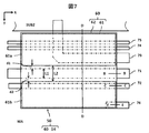
- FIG. 7 is a plan view near the ground pad in FIG. 6.
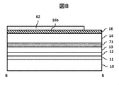
- FIG. 8 is a sectional view taken along the line BB of FIG. 7.
- FIG. 8 is a sectional view taken along the line CC of FIG. 7.
- FIG. 8 is a sectional view taken along the line DD in FIG. 7.
- FIG. 8 is a sectional view taken along the line EE in FIG. 7.
- a liquid crystal display device is disclosed as an example of the display device.
- This liquid crystal display device can be used for various devices such as a smartphone, a tablet terminal, a mobile phone terminal, a personal computer, a television receiver, a vehicle-mounted device, and a game device.
- the terms such as “over” and “below” in describing the drawings represent the relative positional relationship between the structure of interest and another structure. Specifically, when viewed from the side, the direction from the first substrate (array substrate) to the second substrate (counter substrate) is defined as “up”, and the opposite direction is defined as “down”.
- “inside” and “outside” indicate the relative positional relationship between the two parts based on the display area. That is, “inside” indicates a side relatively closer to the display area with respect to one part, and “outside” indicates a side relatively far from the display area with respect to one part.
- the definitions of “inside” and “outside” here are in a state where the liquid crystal display device is not bent.
- Display device refers to all display devices that display images using a display panel.
- Display panel refers to a structure that displays an image using an electro-optic layer.
- the term display panel may refer to a display cell including an electro-optical layer, or to a structure in which another optical member (for example, a polarizing member, a backlight, a touch panel, or the like) is attached to the display cell.
- the “electro-optic layer” may include a liquid crystal layer, an electrochromic (EC) layer, and the like, unless technical contradiction occurs. Therefore, in the embodiments described below, a liquid crystal panel including a liquid crystal layer will be described as an example of a display panel, but application to a display panel including another electro-optical layer described above is not excluded.
- FIG. 1 is a plan view showing the appearance of the display device DSP of the present embodiment.
- the display device DSP includes a display panel PNL, a flexible printed circuit board 1, an IC chip 2, and a circuit board 3.
- the display panel PNL is an IPS type liquid crystal display panel, and includes a first substrate (also referred to as an array substrate) SUB1, a second substrate (also referred to as a counter substrate) SUB2, a liquid crystal layer LC described later, a sealing material SE, It has.
- the display panel PNL includes a display section (display area) DA for displaying an image, and a frame-shaped non-display section (non-display area, frame area) NDA surrounding the display section DA.
- the second substrate SUB2 faces the first substrate SUB1.
- the first substrate SUB1 has a mounting portion MA that extends in the second direction Y from the second substrate SUB2.
- the sealing material SE is located in the non-display portion NDA, and bonds the first substrate SUB1 and the second substrate SUB2 and seals the liquid crystal layer LC.
- the display unit DA includes a plurality of pixels PX arranged in a matrix in the first direction X and the second direction Y.
- the flexible printed circuit board 1 is mounted on the mounting section MA and connected to the circuit board 3.
- the IC chip 2 is mounted on the flexible printed circuit board 1. Note that the IC chip 2 may be mounted on the mounting section MA.
- the IC chip 2 has a built-in display driver DD for outputting a signal necessary for image display in a display mode for displaying an image.
- the display panel PNL of the present embodiment is a transmission type having a transmission display function of displaying an image by selectively transmitting light from the back side of the first substrate SUB1, and light from the front side of the second substrate SUB2.
- the transmittance of the liquid crystal layer LC is changed by rotating the liquid crystal molecules by an electric field (lateral electric field) parallel to the main surfaces of the substrate (SUB1, SUB2). It has viewing angle characteristics.
- the substrate main surface is a surface parallel to the XY plane defined by the first direction X and the second direction Y.
- the display panel PNL has a display mode using a vertical electric field along a normal line of the main surface of the substrate, a display mode using an inclined electric field inclined in an oblique direction with respect to the main surface of the substrate, and the above-described lateral electric field.
- a vertical electric field, and a display mode using a gradient electric field in an appropriate combination may be provided.
- FIG. 1 shows a liquid crystal display panel PNL of the IPS system, in which a shield conductive layer (ITO for shielding) is formed on the back surface or upper side of the counter substrate SUB2.
- a shield conductive layer ITO for shielding
- a ground pad is formed on the mounting portion MA, and the ground pad and the shielding ITO of the counter substrate SUB2 are connected to each other by, for example, a conductive member ( It is electrically connected by a conductor 100.
- a conductive tape, a conductive resin, a conductive paste, or the like can be used as the conductive member 100.
- the conductive tape has a configuration in which, for example, an adhesive material in which conductive fine particles are dispersed is formed on one surface of a tape of a metal such as aluminum (Al) or copper (Cu).
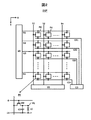
- FIG. 2 is a diagram illustrating a basic configuration of the pixel PX and an equivalent circuit of the display device DSP.
- the plurality of pixels PX are arranged in a matrix in the first direction X and the second direction Y.
- the plurality of scanning lines G (G1, G2,...) Are connected to a scanning line driving circuit GD.
- the plurality of signal lines S (S1, S2,%) are connected to a signal line driving circuit SD.
- the plurality of common electrodes CE CE1, CE2,...) are connected to a voltage supply unit CD for a common voltage (Vcom), and are arranged over a plurality of pixels PX.
- One pixel PX is connected to one scanning line, one signal line, and one common electrode CE.
- the scanning lines G and the signal lines S do not necessarily need to extend linearly, and some of them may be bent. For example, it is assumed that the signal line S extends in the second direction Y even if a part thereof is bent.
- Each pixel PX includes a switching element SW, a pixel electrode PE, a common electrode CE, a liquid crystal layer LC, and the like.
- the switching element SW is composed of, for example, a thin film transistor (TFT), and is electrically connected to the scanning line G and the signal line S.
- the scanning line G is connected to the switching element SW in each of the pixels PX arranged in the first direction X.
- the signal line S is connected to the switching element SW in each of the pixels PX arranged in the second direction Y.
- the pixel electrode PE is electrically connected to the switching element SW.
- Each of the pixel electrodes PE faces the common electrode CE, and drives the liquid crystal layer LC by an electric field generated between the pixel electrode PE and the common electrode CE.
- the storage capacitor CS is formed, for example, between an electrode having the same potential as the common electrode CE and an electrode having the same potential as the pixel electrode PE.
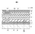
- FIG. 3 is a cross-sectional view of the first substrate SUB1 in the display area DA of the display panel PLN.
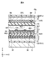
- FIG. 4 is a sectional view of the display area DA of the display panel PLN. 3 and 4 are described using reference numbers such as the scanning line G2, the signal lines S5 and S6, and the pixel electrode PE11, for example, but are not limited thereto.
- a first substrate SUB1 is formed of an insulating substrate 10, insulating films 11 to 16, a semiconductor layer SC, a scanning line (first metal wiring) G2 formed of a first metal layer, and a second metal layer.
- a pixel electrode (second transparent electrode) PE11 formed of two transparent conductive films, an alignment film AL1, and the like are provided.
- the pixel electrode PE11 will be described later with reference to FIG.
- the insulating substrate 10 is a substrate having optical transparency, such as a glass substrate or a flexible resin substrate.
- the insulating film 11 is located on the insulating substrate 10.
- the semiconductor layer SC is located on the insulating film 11 and is covered by the insulating film 12.
- the semiconductor layer SC is formed of, for example, polycrystalline silicon, but may be formed of amorphous silicon or an oxide semiconductor.
- the gate electrode GE1 which is a part of the scanning line G2, is located on the insulating film 12 and is covered with the insulating film (inorganic insulating film) 13. Note that other scanning lines (not shown) are also located on the same layer as the scanning line G2.
- the scanning line G2 is made of a metal material such as aluminum (Al), titanium (Ti), silver (Ag), molybdenum (Mo), tungsten (W), copper (Cu), chromium (Cr), or a metal material such as these. It may be formed of a combined alloy or the like, and may have a single-layer structure or a multilayer structure. In one example, the scanning line G2 is formed of a molybdenum-tungsten alloy.
- the signal line S6 is located on the insulating film 13 and is covered by the insulating film (first organic insulating film). Note that other signal lines not shown are also located in the same layer as the signal line S6.
- the signal line S6 is formed of the above-mentioned metal material, an alloy obtained by combining the above-described metal materials, or the like, and may have a single-layer structure or a multilayer structure. In one example, the signal line S6 is a laminate in which titanium (Ti), aluminum (Al), and titanium (Ti) are laminated in this order.
- the signal line S6 is in contact with the semiconductor layer SC through a contact hole CH1 penetrating the insulating films 12 and 13.
- the metal wiring ML6 is located on the insulating film 14 and is covered by the insulating film (second organic insulating film) 15.
- the metal wiring ML6 is formed of the above-mentioned metal material, an alloy obtained by combining the above-described metal materials, or the like, and may have a single-layer structure or a multilayer structure.
- the metal wiring ML6 is formed by stacking titanium (Ti), aluminum (Al), and titanium (Ti) in this order, or by using molybdenum (Mo), aluminum (Al), and molybdenum (Mo). ) Is a laminated body laminated in this order.
- the common electrode CE is located on the insulating film 15 and is covered by the insulating film (inorganic insulating film) 16.
- the common electrode CE is a transparent electrode formed of a transparent conductive material such as indium tin oxide (ITO) or indium zinc oxide (IZO).
- ITO indium tin oxide
- IZO indium zinc oxide
- the common electrode CE is in contact with the metal wiring ML6 through a contact hole CH3 penetrating the insulating film 15.
- the alignment film AL1 is located on the insulating film 16.
- Each of the insulating films 11 to 13 and the insulating film 16 is an inorganic insulating film formed using an inorganic insulating material such as silicon oxide, silicon nitride, or silicon oxynitride, and may have a single-layer structure. It may have a multilayer structure.
- the insulating film 14 is, for example, an organic insulating film (first organic insulating film) formed of an organic insulating material such as an acrylic resin.
- the insulating film 15 is, for example, an organic insulating film (a second organic insulating film) formed of an organic insulating material such as an acrylic resin. Note that the insulating film 15 may be an inorganic insulating film.
- the insulating film 14 has a thickness of, for example, about 2.5 ⁇ m.
- the insulating film 15 has a thickness of, for example, about 1.5 ⁇ m.
- the signal lines S5 and S6 are located on the insulating film 13 and covered with the insulating film.
- the metal wirings ML5 and ML6 are located immediately above the signal lines S5 and S6, respectively.
- the pixel electrode PE11 is located on the insulating film 16 and is covered by the alignment film AL1.
- the pixel electrode PE11 is a transparent electrode formed of a transparent conductive material such as ITO and IZO.
- the second substrate SUB2 includes a shield conductive layer (ITO for shielding) 19, an insulating substrate 20, a light shielding layer BM, a color filter CFG, an overcoat layer OC, an alignment film AL2, and the like.
- ITO shield conductive layer
- the shield conductive layer 19 is made of a transparent conductive material such as indium tin oxide (ITO) or indium zinc oxide (IZO).
- the shield conductive layer 19 is located outside the insulating substrate 20.
- the insulating substrate 20, like the insulating substrate 10, is a light-transmitting substrate such as a glass substrate or a resin substrate.
- the light-blocking layer BM and the color filter CFG are located on the side of the insulating substrate 20 facing the first substrate SUB1.
- the color filter CFG is arranged at a position facing the pixel electrode PE11, and a part of the color filter CFG overlaps the light shielding layer BM.
- the overcoat layer OC covers the green color filter CFG.
- the overcoat layer OC is formed of a transparent resin.
- the other red and blue color filters are arranged at positions facing the pixel electrodes PE, respectively, and are covered with the overcoat layer OC.
- the alignment film AL2 covers the overcoat layer OC.
- the alignment film AL1 and the alignment film AL2 are formed, for example, of a material exhibiting horizontal alignment.
- the first substrate SUB1 and the second substrate SUB2 described above are arranged such that the alignment films AL1 and AL2 face each other.
- the main spacer and the sub spacer are formed of a resin material, and are disposed between the first substrate SUB1 and the second substrate SUB2.
- the main spacer forms a predetermined cell gap between the alignment films AL1 and AL2.
- the cell gap is, for example, 2 to 5 ⁇ m.
- the first substrate SUB1 and the second substrate SUB2 are bonded with a sealing material in a state where a predetermined cell gap is formed.
- the liquid crystal layer LC is located between the first substrate SUB1 and the second substrate SUB2, and is held between the alignment films AL1 and AL2.
- the liquid crystal layer LC includes liquid crystal molecules LM.
- the liquid crystal layer LC is formed of a positive liquid crystal material (having a positive dielectric anisotropy) or a negative liquid crystal material (having a negative dielectric anisotropy).
- the optical element OD1 including the polarizing plate PL1 is bonded to the insulating substrate 10.
- the optical element OD2 including the polarizing plate PL2 is bonded to the shield conductive layer 19.
- the optical element OD1 and the optical element OD2 may include a retardation plate, a scattering layer, an anti-reflection layer, and the like, if necessary.
- the liquid crystal molecules LM In such a display panel PNL, in an off state where no electric field is formed between the pixel electrode PE and the common electrode CE, the liquid crystal molecules LM initially move in a predetermined direction between the alignment films AL1 and AL2. Oriented. In such an off state, light emitted from the illumination device IL toward the display panel PNL is absorbed by the optical elements OD1 and OD2, and a dark display is obtained. On the other hand, in the ON state in which an electric field is formed between the pixel electrode PE and the common electrode CE, the liquid crystal molecules LM are oriented in a direction different from the initial orientation direction by the electric field, and the orientation direction is controlled by the electric field. . In such an ON state, a part of the light from the illumination device IL passes through the optical elements OD1 and OD2, and a bright display is obtained.
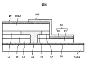
- FIG. 5 is a cross-sectional view of the vicinity of the ground pad in the present embodiment.
- FIG. 5 is a cross-sectional view taken along line AA of FIG.
- the first substrate SUB1 and the second substrate SUB2 are adhered by a sealing material SE, and the liquid crystal layer LC is sandwiched between the first substrate SUB1 and the second substrate SUB2.
- the wall-shaped spacer SP is formed at an end of the second substrate SUB2. Only the organic insulating films 14 and 15 are described for the layer on the first substrate SUB1 side.
- a groove 40 is formed in the organic insulating films 14 and 15 at a portion overlapping with the sealing material SE. This is to prevent moisture from entering from outside through the organic insulating films 14 and 15.
- the organic insulating film 14 extends to a portion where the ground pad 50 is formed in the mounting portion MA.
- the connection transparent conductive film 60 is formed on the organic insulating film 14, thereby forming the ground pad 50.
- the area under the ground pad 50 can be used as a wiring area, and the area of the mounting portion MA can be reduced accordingly.
- a wiring 70 passing below the ground pad 50 is shown as an example.
- the wiring 70 may include a wiring for leading a video signal line, a wiring for a power supply, a wiring for inspection, and the like.
- connection transparent conductive film 60 of the ground pad 50 is connected by wiring to an external connection terminal (GND) for power supply provided on the mounting part MA of the first substrate SUB1.
- a reference potential such as a ground potential or a ground potential is supplied to the external connection terminal (GND).
- FIG. 6 is a plan view showing the appearance of the display device DSP in a state where the conductive tape does not exist.
- FIG. 6 shows a state before the shield conductive layer 19 and the ground pad 50 are connected by the conductive tape 100.
- a ground pad 50 is formed in a portion adjacent to the second substrate SUB2.
- the ground pad 50 includes the organic insulating film 14 and the connecting transparent conductive film 60 formed thereon.
- Other configurations are the same as those described with reference to FIG.
- FIG. 7 is a plan view of the vicinity of the ground pad 50 in FIG.
- FIG. 8 is a sectional view taken along line BB of FIG.
- FIG. 9 is a sectional view taken along the line CC of FIG.
- FIG. 10 is a sectional view taken along line DD in FIG.
- FIG. 11 is a sectional view taken along line EE in FIG.
- a ground pad 50 is provided adjacent to second substrate SUB2 in plan view.
- the ground pad 50 has a rectangular shape, but may have another planar shape.
- the ground pad 50 is formed by forming a transparent conductive film 60 for connection on the organic insulating film 14. Under the organic insulating film 14, first to fifth wirings (71 to 75) are formed.
- the first wiring 71, the second wiring 72, the fourth wiring 74, and the fifth wiring 75 extend linearly in the first direction X in plan view, and extend below the ground pad 50. It is provided so as to cross.
- the third wiring 73 has a first wiring part provided along the first direction X and a second wiring part provided along the second direction Y.
- the wiring portion provided along the second direction Y of the third wiring 73 is provided so as to pass over the fourth wiring 74 and the fifth wiring 75. Therefore, the third wiring 73 is a wiring that crosses the fourth wiring 74 and the fifth wiring 75 in a plan view.
- the first to third wirings 71 to 73 are formed by the same wiring layer as the signal lines S5 and S6.
- the fourth wiring 74 and the fifth wiring 75 are formed by the same wiring layer as the scanning line G2.
- the first wiring 71 is supplied with a first reference potential such as a power supply potential (Vdd) or 7V.
- the first wiring 71 is, for example, a power supply wiring for supplying a high potential voltage of the scanning line G2.
- the third wiring 73 is supplied with a second reference potential lower than the first reference potential, such as ground potential (GND) or 0V.
- the third wiring 73 is, for example, a power supply wiring for supplying a low potential voltage of the scanning line G2.
- the first wiring 71 and the third wiring 73 are relatively thick in plan view as compared with the second wiring 72 and the fourth and fifth wirings 74 and 75. Since the relatively thick wiring such as the power supply wiring is arranged in the wiring area below the ground pad 50, the area of the mounting portion MA can be reduced accordingly.
- the sixth wiring 76 is provided to supply a ground potential or a reference potential such as a ground potential to the ground pad 50.
- One end of the sixth wiring 76 is electrically connected to the connecting transparent conductive film 60 of the ground pad 50.
- the other end of the sixth wiring 76 is connected to an external connection terminal (GND) provided on the mounting part MA of the first substrate SUB1.
- a reference potential such as a ground potential or a ground potential is supplied to the external connection terminal (GND).
- the connection transparent conductive film 60 includes a first connection transparent conductive film 61 and a second connection transparent conductive film 62.
- the first connection transparent conductive film 61 is located in the same layer as the common electrode CE, and is formed of the same material as the common electrode CE.
- the second connection transparent conductive film 62 is located in the same layer as the pixel electrode PE11, and is formed of the same material as the pixel electrode PE11.
- the second connection transparent conductive film 62 is formed on the first connection transparent conductive film 61, and the first connection transparent conductive film 61 and the second connection transparent conductive film 62 are electrically connected. .
- the first connection transparent conductive film 61 is provided divided into the first electrode portion 61a and the second electrode portion 61b.
- the second connection transparent conductive film 62 is provided in the region of the ground pad 50 corresponding to the upper side of the first wiring 71. Not provided.
- the transparent conductive film 62 for the second connection and the transparent conductive film 61 for the first connection are provided in the region of the ground pad 50 corresponding to the upper side of the second to fifth wirings (72-75). Both are provided in layers.
- the width L1 of the first wiring 71 in the second direction Y is smaller than the distance L2 between the first electrode portion 61a and the second electrode portion 61b in the second direction Y (L1 ⁇ L2).
- the first wiring 71 having the width L1 is disposed between the first electrode portion 61a and the second electrode portion 61b in the interval L2 in the second direction Y. That is, the first connection transparent conductive film 61 is provided so as to avoid over the first wiring 71 in plan view. Therefore, the first connection transparent conductive film 61 is divided into a first electrode portion 61a and a second electrode portion 61b.
- the distance d1 between the upper end of the first wiring 71 and the lower end of the first electrode portion 61a, and the lower end of the first wiring 71 and the second electrode portion It is preferable that the interval d2 between the upper ends of the upper portions 61b is, for example, about 5 ⁇ m.
- the present invention is not limited thereto.
- the first wiring 71 is provided at a position adjacent to the second substrate SUB2 along the edge of the second substrate SUB2, it is not necessary to divide the first connection transparent conductive film 61.
- the first connection transparent conductive film 61 can be divided into two or more. .
- FIG. 8 is a cross-sectional view taken along the line BB of FIG.
- the first wiring 71 is located in the same layer as the signal lines S5 and S6, and is formed of the same material as the signal lines S5 and S6.
- the first wiring 71 is formed on the insulating film 13, and the first wiring 71 is covered with the organic insulating film 14.
- the organic insulating film 14 is covered with an insulating film 16 formed of an inorganic insulating material.
- the second connection transparent conductive film 62 is provided on the insulating film 16.
- the insulating film 16 located under the second connection transparent conductive film 62 is shown as an insulating film 16b.
- the insulating film 16b will be described later with reference to FIG.
- the first connection transparent conductive film 61 is not provided and only the second connection transparent conductive film 62 is provided over the entire area where the first wiring 71 is disposed.
- FIG. 9 is a cross-sectional view taken along the line CC of FIG. 7, and is a cross-sectional view of an arrangement portion of the second wiring 72.
- the second wiring 72 is located in the same layer as the signal lines S5 and S6, and is formed of the same material as the signal lines S5 and S6.
- the second wiring 72 is formed on the insulating film 13, and the upper part of the second wiring 72 is covered with the organic insulating film 14.
- the second electrode portion 61b of the first connection transparent conductive film 61 is selectively provided on the organic insulating film 14.
- the insulating film 16 is provided so as to cover the end of the second electrode portion 61b and the portion of the organic insulating film 14 where the second electrode portion 61b is not formed.
- the second connection transparent conductive film 62 is provided on the second electrode portion 61b and on the insulating film 16 covering the end of the second electrode portion 61b.
- both the first connection transparent conductive film 61 and the second connection transparent conductive film 62 are provided in a stacked manner over the entire area where the second wiring 72 is disposed.
- first to third wirings 71 to 73 are arranged on insulating film 13
- fourth and fifth wirings 74 and 75 are arranged on insulating film 12.
- the first to third wirings 71 to 73 are located in the same layer as the signal lines S5 and S6, and are formed of the same material as the signal lines S5 and S6.
- the fourth and fifth wirings 74 and 75 are located in the same layer as the scanning line G2 and are formed of the same material as the scanning line G2.
- a first electrode portion 61a of the first connection transparent conductive film 61 is provided above the third to fifth wirings 73-75.
- the second electrode portion 61b of the first connection transparent conductive film 61 is provided above the second wiring 72.
- the first connection transparent conductive film 61 is not provided above the first wiring 71.
- An insulating film 16b is provided between the first electrode portion 61a and the second electrode portion 61b of the first connection transparent conductive film 61.
- the insulating film 16 b is the same insulating film as the insulating film 16.
- the insulating film 16b is formed on the surface of the organic insulating film 14 exposed from between the first electrode portion 61a and the second electrode portion 61b, and on opposite ends of the first electrode portion 61a and the second electrode portion 61b. Is provided so as to cover.
- the second connection transparent conductive film 62 is provided on the first electrode portion 61a, the second electrode portion 61b, and the insulating film 16b, and includes the first electrode portion 61a, the second electrode portion 61b, and the second connection portion. Transparent conductive film 62 is electrically connected.
- the second transparent conductive film 62 for connection is formed on the first electrode portion 61a exposed from the openings O1 provided in the insulating films 16 and 16b, and on the first electrode portion 61a exposed from the openings O2 provided in the insulating films 16 and 16b. It is provided so as to cover the two electrode portions 61b, the insulating film 16b, and the ends of the insulating films 16 on both sides.
- the first connection transparent conductive film 61 and the second connection transparent conductive film 62 of the ground pad 50 can be formed, for example, as follows.
- a transparent conductive film is formed on the organic insulating film 14 at the same time as the formation of the common electrode CE, and the formed transparent conductive film is patterned to form the first connection transparent conductive film.
- the first electrode portion 61a and the second electrode portion 61b of the film 61 are selectively formed.
- the insulating film 16 is formed in a region where the ground pad 50 is formed, and the insulating film 16 is patterned to form openings O1 and O2 in the insulating film 16. Thereby, the first electrode portion 61a and the second electrode portion 61b are selectively exposed.
- a transparent conductive film is formed in the formation region of the ground pad 50 simultaneously with the formation of the pixel electrode PE11, and the transparent conductive film is patterned to form the second connection transparent conductive film 62.
- an energization test may be performed in a high temperature and high humidity state.
- the high temperature is 85 ° C. and the high humidity is a relative humidity of 85% RH.
- the energization test is a test in which the display device DSP is operated for a long time (for example, 240 hours) in an operation state in which the same power supply potential as the actual operation is supplied.
- the low-potential first connection transparent conductive film 61 does not exist above the first wiring 71 that is the high-potential power supply wiring, and the insulating films 14 and 16 are not provided.
- a second connection transparent conductive film 62 is provided.
- FIG. 11 is a cross-sectional view taken along the line EE in FIG.
- the sixth wiring 76 is located in the same layer as the scanning line G2 and is formed of the same material as the scanning line G2, and is located in the same layer as the signal lines S5 and S6 and the same material as the signal lines S5 and S6. It has a laminated structure with the wiring 762 formed.
- One end of the sixth wiring 76, that is, one end of the wiring 762 is connected to the first electrode portion 61 a of the first transparent conductive film 61 for connection.
- the other end of the sixth wiring 76 is connected to an external connection terminal (GND) provided on the mounting part MA.
- GND external connection terminal
- the corrosion of the ground pad 50 can be prevented, and the area of the mounting part MA is reduced. be able to.
- the frame area of the display device can be narrowed.
- ⁇ ⁇ Various inventions can be formed by appropriately combining a plurality of constituent elements disclosed in the above embodiments. For example, some components may be deleted from all the components shown in the embodiment. Further, components of different embodiments may be appropriately combined.
- DSP display device PNL: display panel
- SUB1 first substrate (array substrate)
- SUB2 Second substrate (counter substrate)
- Organic insulating film 19 Shield conductive layer 50: Earth pad
- 60 Transparent conductive film 61 for connection: First transparent conductive film 61a for connection: First electrode portion 61b: Second electrode portion 62: Transparent conductive film for second connection Film
- 71 first wiring (power supply wiring)
- 72 second wiring 100: conductor (conductive tape)
Landscapes
- Physics & Mathematics (AREA)
- Nonlinear Science (AREA)
- General Physics & Mathematics (AREA)
- Crystallography & Structural Chemistry (AREA)
- Chemical & Material Sciences (AREA)
- Mathematical Physics (AREA)
- Optics & Photonics (AREA)
- Engineering & Computer Science (AREA)
- Microelectronics & Electronic Packaging (AREA)
- Theoretical Computer Science (AREA)
- Geometry (AREA)
- Computer Hardware Design (AREA)
- Liquid Crystal (AREA)
- Devices For Indicating Variable Information By Combining Individual Elements (AREA)
Abstract
本発明の目的は、表示装置の信頼性を向上することが可能な構成を提供することにある。表示装置は、パッドを有する第1基板と、シールド導電層を有する第2基板と、前記パッドと前記シールド導電層とに接続された導電体と、を含む。前記第1基板は、前記パッドの下に設けられた第1配線を含み、前記パッドは、前記第1配線を覆う様に設けられた有機絶縁膜と、前記有機絶縁膜の上に設けられた透明導電膜と、を含む。前記透明導電膜は、前記有機絶縁膜の上に設けられた第1透明導電膜と、前記第1透明導電膜に接続された第2透明導電膜と、を含む。前記第1透明導電膜は、平面視において、前記第1配線の上を回避するように設けられ、前記第2透明電極膜は、平面視において、前記第1配線の上、および、前記第1透明電極膜の上を覆う様に設けられる。
Description
本発明は表示装置に関し、特に、IPS方式の表示装置に適用可能である。
IPS(In Plane Switchin)方式の表示装置では、ノイズ防止のため、対向基板の外側にシールド用透明導電層を形成し、シールド用透明導電層をTFT基板側に設けたアースパッドに、導電性テープで接続することが行われる(特開2017-146450号公報参照)。
表示装置の表示パネルは、一般的に、複数の画素が形成された表示領域と、表示領域の外周を囲む様に設けられた額縁領域と、を有する。近年、たとえば、スマートフォンや携帯電話などにおいて、額縁領域を狭くし、表示パネルを上面から見た場合の表示領域の割合を大面積化することが行われている。
IPS方式の表示装置において、額縁領域が狭くされた場合、アースパッドの下側に、電源配線、検査用配線などの各種の配線を配置する場合がある。
アースパッドの下側に、高電位の電源配線が配置された構成において、高温高湿の環境下において、表示装置に電源を供給して動作させる様な通電試験を実施すると、アースパッドの構成に起因して、アースパッドに腐食が発生する場合があることを、発明者は見出した。つまり、アースパッドと電源配線との電位差により、アースパッドと電源配線との間に縦電界が生じる。この縦電界と水分との影響により、アースパッドに腐食が発生する。
本発明の目的は、表示装置の信頼性を向上することが可能な構成を提供することにある。
その他の課題と新規な特徴は、本明細書の記述および添付図面から明らかになるであろう。
本発明のうち代表的なものの概要を簡単に説明すれば下記の通りである。
すなわち、表示装置は、パッドを有する第1基板と、シールド導電層を有する第2基板と、前記パッドと前記シールド導電層とに接続された導電体と、を含む。前記第1基板は、前記パッドの下に設けられた第1配線を含み、前記パッドは、前記第1配線を覆う様に設けられた有機絶縁膜と、前記有機絶縁膜の上に設けられた透明導電膜と、を含む。前記透明導電膜は、前記有機絶縁膜の上に設けられた第1透明導電膜と、前記第1透明導電膜に接続された第2透明導電膜と、を含む。前記第1透明導電膜は、平面視において、前記第1配線の上を回避するように設けられ、前記第2透明電極膜は、平面視において、前記第1配線の上、および、前記第1透明電極膜の上を覆う様に設けられる。
以下に、本発明の各実施の形態について、図面を参照しつつ説明する。
なお、開示はあくまで一例にすぎず、当業者において、発明の主旨を保っての適宜変更について容易に想到し得るものについては、当然に本発明の範囲に含有されるものである。また、図面は説明をより明確にするため、実際の態様に比べ、各部の幅、厚さ、形状等について模式的に表される場合があるが、あくまで一例であって、本発明の解釈を限定するものではない。
また、本明細書と各図において、既出の図に関して前述したものと同様の要素には、同一の符号を付して、詳細な説明を適宜省略することがある。
本実施形態においては、表示装置の一例として、液晶表示装置を開示する。この液晶表示装置は、例えば、スマートフォン、タブレット端末、携帯電話端末、パーソナルコンピュータ、テレビ受像装置、車載装置、ゲーム機器等の種々の装置に用いることができる。
なお、本明細書及び請求の範囲において、図面を説明する際の「上」、「下」などの表現は、着目する構造体と他の構造体との相対的な位置関係を表現している。具体的には、側面から見た場合において、第1基板(アレイ基板)から第2基板(対向基板)に向かう方向を「上」と定義し、その逆の方向を「下」と定義する。
また、「内側」及び「外側」とは、2つの部位における、表示領域を基準とした相対的な位置関係を示す。すなわち、「内側」とは、一方の部位に対し相対的に表示領域に近い側を指し、「外側」とは、一方の部位に対し相対的に表示領域から遠い側を指す。ただし、ここで言う「内側」及び「外側」の定義は、液晶表示装置を折り曲げていない状態におけるものとする。
「表示装置」とは、表示パネルを用いて映像を表示する表示装置全般を指す。「表示パネル」とは、電気光学層を用いて映像を表示する構造体を指す。例えば、表示パネルという用語は、電気光学層を含む表示セルを指す場合もあるし、表示セルに対して他の光学部材(例えば、偏光部材、バックライト、タッチパネル等)を装着した構造体を指す場合もある。ここで、「電気光学層」には、技術的な矛盾を生じない限り、液晶層、エレクトロクロミック(EC)層などが含まれ得る。したがって、後述する実施形態について、表示パネルとして、液晶層を含む液晶パネルを例示して説明するが、上述した他の電気光学層を含む表示パネルへの適用を排除するものではない。
(表示装置の全体構成例)
図1は、本実施形態の表示装置DSPの外観を示す平面図である。表示装置DSPは、表示パネルPNLと、フレキシブルプリント回路基板1と、ICチップ2と、回路基板3と、を備えている。表示パネルPNLは、IPS方式の液晶表示パネルであり、第1基板(アレイ基板ともいう)SUB1と、第2基板(対向基板ともいう)SUB2と、後述する液晶層LCと、シール材SEと、を備えている。
図1は、本実施形態の表示装置DSPの外観を示す平面図である。表示装置DSPは、表示パネルPNLと、フレキシブルプリント回路基板1と、ICチップ2と、回路基板3と、を備えている。表示パネルPNLは、IPS方式の液晶表示パネルであり、第1基板(アレイ基板ともいう)SUB1と、第2基板(対向基板ともいう)SUB2と、後述する液晶層LCと、シール材SEと、を備えている。
表示パネルPNLは、画像を表示する表示部(表示領域)DAと、表示部DAを囲む額縁状の非表示部(非表示領域、額縁領域)NDAと、を備えている。第2基板SUB2は、第1基板SUB1に対向している。第1基板SUB1は、第2基板SUB2よりも第2方向Yに延出した実装部MAを有している。シール材SEは、非表示部NDAに位置し、第1基板SUB1と第2基板SUB2とを接着するとともに、液晶層LCを封止している。
表示部DAは、第1方向X及び第2方向Yにマトリクス状に配置された複数の画素PXを備えている。
フレキシブルプリント回路基板1は、実装部MAに実装され、回路基板3に接続されている。ICチップ2は、フレキシブルプリント回路基板1に実装されている。なお、ICチップ2は、実装部MAに実装されてもよい。ICチップ2は、画像を表示する表示モードにおいて画像表示に必要な信号を出力するディスプレイドライバDDを内蔵している。
本実施形態の表示パネルPNLは、第1基板SUB1の背面側からの光を選択的に透過させることで画像を表示する透過表示機能を備えた透過型、第2基板SUB2の前面側からの光を選択的に反射させることで画像を表示する反射表示機能を備えた反射型、あるいは、透過表示機能及び反射表示機能を備えた半透過型のいずれであってもよい。
IPS(In Plane Switchin)方式の場合、基板主面(SUB1、SUB2)と平行方向の電界(横電界)によって液晶分子を回転させることによって、液晶層LCの透過率を変えるものであり、優れた視野角特性を有している。IPS方式では、基本的には、対向基板SUB2には対向電極を形成する必要がない。ここでの基板主面とは、第1方向X及び第2方向Yで規定されるX-Y平面と平行な面である。表示パネルPNLは、また、基板主面の法線に沿った縦電界を利用する表示モード、基板主面に対して斜め方向に傾斜した傾斜電界を利用する表示モード、さらには、上記の横電界、縦電界、及び、傾斜電界を適宜組み合わせて利用する表示モードに対応したいずれの構成を備えていてもよい。
図1はIPS方式の液晶表示パネルPNLであり、対向基板SUB2の裏面または上側にはシールド導電層(シールド用ITO)が形成されている。シールド用ITOをアース電位あるいは接地電位のような基準電位と接続するために、実装部MAにアースパッドを形成し、このアースパッドと対向基板SUB2のシールド用ITOとを、例えば、導電性部材(導電体)100で電気的に接続する。導電性部材100は、導電性テープ、導電性樹脂、導電性ペースト等を利用することができる。導電性テープは、例えば、アルミニウム(Al)、銅(Cu)等の金属のテープの一方の面に、導電性微粒子が分散された粘着材が形成された構成となっている。
(表示装置の回路構成例)
図2は、画素PXの基本構成及び表示装置DSPの等価回路を示す図である。複数の画素PXは、第1方向X及び第2方向Yにマトリクス状に配置されている。複数本の走査線G(G1、G2・・・)は、走査線駆動回路GDに接続されている。複数本の信号線S(S1、S2・・・)は、信号線駆動回路SDに接続されている。複数本の共通電極CE(CE1、CE2・・・)は、コモン電圧(Vcom)の電圧供給部CDに接続され、複数の画素PXに亘って配置されている。1つの画素PXは、1本の走査線と、1本の信号線と、1本の共通電極CEと、に接続されている。なお、走査線G及び信号線Sは、必ずしも直線的に延出していなくてもよく、それらの一部が屈曲していてもよい。例えば、信号線Sは、その一部が屈曲していたとしても、第2方向Yに延出しているものとする。
図2は、画素PXの基本構成及び表示装置DSPの等価回路を示す図である。複数の画素PXは、第1方向X及び第2方向Yにマトリクス状に配置されている。複数本の走査線G(G1、G2・・・)は、走査線駆動回路GDに接続されている。複数本の信号線S(S1、S2・・・)は、信号線駆動回路SDに接続されている。複数本の共通電極CE(CE1、CE2・・・)は、コモン電圧(Vcom)の電圧供給部CDに接続され、複数の画素PXに亘って配置されている。1つの画素PXは、1本の走査線と、1本の信号線と、1本の共通電極CEと、に接続されている。なお、走査線G及び信号線Sは、必ずしも直線的に延出していなくてもよく、それらの一部が屈曲していてもよい。例えば、信号線Sは、その一部が屈曲していたとしても、第2方向Yに延出しているものとする。
各画素PXは、スイッチング素子SW、画素電極PE、共通電極CE、液晶層LC等を備えている。スイッチング素子SWは、例えば薄膜トランジスタ(TFT)によって構成され、走査線G及び信号線Sと電気的に接続されている。走査線Gは、第1方向Xに並んだ画素PXの各々におけるスイッチング素子SWと接続されている。信号線Sは、第2方向Yに並んだ画素PXの各々におけるスイッチング素子SWと接続されている。画素電極PEは、スイッチング素子SWと電気的に接続されている。画素電極PEの各々は、共通電極CEと対向し、画素電極PEと共通電極CEとの間に生じる電界によって液晶層LCを駆動している。保持容量CSは、例えば、共通電極CEと同電位の電極、及び、画素電極PEと同電位の電極の間に形成される。
(表示領域の断面構成例)
図3は、表示パネルPLNの表示領域DAにおける第1基板SUB1の断面図である。図4は、表示パネルPLNの表示領域DAの断面図である。なお、図3および図4は、例示的に、走査線G2、信号線S5、S6、画素電極PE11の等の参照番号を用いて説明するが、それに限定されるわけではない。
図3は、表示パネルPLNの表示領域DAにおける第1基板SUB1の断面図である。図4は、表示パネルPLNの表示領域DAの断面図である。なお、図3および図4は、例示的に、走査線G2、信号線S5、S6、画素電極PE11の等の参照番号を用いて説明するが、それに限定されるわけではない。
図3を参照し、第1基板SUB1は、絶縁基板10、絶縁膜11乃至16、半導体層SC、第1金属層で形成される走査線(第1金属配線)G2、第2金属層で形成される信号線(第2金属配線)S6、第3金属層で形成される金属配線(第3金属配線)ML6、第1透明導電膜で形成される共通電極(第1透明電極)CE、第2透明導電膜で形成される画素電極(第2透明電極)PE11、配向膜AL1などを備えている。なお、画素電極PE11は後述する図4にて説明する。
絶縁基板10は、ガラス基板や可撓性の樹脂基板などの光透過性を有する基板である。絶縁膜11は、絶縁基板10の上に位置している。半導体層SCは、絶縁膜11の上に位置し、絶縁膜12によって覆われている。半導体層SCは、例えば、多結晶シリコンによって形成されているが、アモルファスシリコンや酸化物半導体によって形成されていてもよい。
走査線G2の一部であるゲート電極GE1は、絶縁膜12の上に位置し、絶縁膜(無機絶縁膜)13によって覆われている。なお、図示しない他の走査線も、走査線G2と同一層に位置している。走査線G2は、アルミニウム(Al)、チタン(Ti)、銀(Ag)、モリブデン(Mo)、タングステン(W)、銅(Cu)、クロム(Cr)などの金属材料や、これらの金属材料を組み合わせた合金などによって形成され、単層構造であってもよいし、多層構造であってもよい。一例では、走査線G2は、モリブデン-タングステン合金によって形成されている。
信号線S6は、絶縁膜13の上に位置し、絶縁膜(第1有機絶縁膜)14によって覆われている。なお、図示しない他の信号線も、信号線S6と同一層に位置している。信号線S6は、上記の金属材料や、上記の金属材料を組み合わせた合金などによって形成され、単層構造であってもよいし、多層構造であってもよい。一例では、信号線S6は、チタン(Ti)、アルミニウム(Al)、及び、チタン(Ti)がこの順に積層された積層体である。信号線S6は、絶縁膜12及び絶縁膜13を貫通するコンタクトホールCH1を通じて半導体層SCにコンタクトしている。
金属配線ML6は、絶縁膜14の上に位置し、絶縁膜(第2有機絶縁膜)15によって覆われている。金属配線ML6は、上記の金属材料や、上記の金属材料を組み合わせた合金などによって形成され、単層構造であってもよいし、多層構造であってもよい。一例では、金属配線ML6は、チタン(Ti)、アルミニウム(Al)、及び、チタン(Ti)がこの順に積層された積層体、あるいは、モリブデン(Mo)、アルミニウム(Al)、及び、モリブデン(Mo)がこの順に積層された積層体である。
共通電極CEは、絶縁膜15の上に位置し、絶縁膜(無機絶縁膜)16によって覆われている。共通電極CEは、インジウム・ティン・オキサイド(ITO)やインジウム・ジンク・オキサイド(IZO)などの透明な導電材料によって形成された透明電極である。共通電極CEは、絶縁膜15を貫通するコンタクトホールCH3を通じて金属配線ML6にコンタクトしている。配向膜AL1は、絶縁膜16の上に位置している。
絶縁膜11乃至13、及び、絶縁膜16は、シリコン酸化物、シリコン窒化物、シリコン酸窒化物などの無機絶縁材料によって形成された無機絶縁膜であり、単層構造であってもよいし、多層構造であってもよい。絶縁膜14は、例えば、アクリル樹脂などの有機絶縁材料によって形成された有機絶縁膜(第1有機絶縁膜)である。絶縁膜15は、例えば、アクリル樹脂などの有機絶縁材料によって形成された有機絶縁膜(第2有機絶縁膜)である。なお、絶縁膜15は、無機絶縁膜であってもよい。絶縁膜14は、たとえば、2.5μm程度の膜厚である。絶縁膜15は、たとえば、1.5μm程度の膜厚である。
図4を参照し、第1基板SUB1において、信号線S5及びS6は、絶縁膜13の上に位置し、絶縁膜14によって覆われている。金属配線ML5及びML6は、それぞれ信号線S5及びS6の直上に位置している。画素電極PE11は、絶縁膜16の上に位置し、配向膜AL1によって覆われている。画素電極PE11は、ITOやIZOなどの透明な導電材料によって形成された透明電極である。
第2基板SUB2は、シールド導電層(シールド用ITO)19、絶縁基板20、遮光層BM、カラーフィルタCFG、オーバーコート層OC、配向膜AL2などを備えている。
シールド導電層19は、インジウム・ティン・オキサイド(ITO)やインジウム・ジンク・オキサイド(IZO)などの透明な導電材料によって形成されている。シールド導電層19は、絶縁基板20の外側に位置している。絶縁基板20は、絶縁基板10と同様に、ガラス基板や樹脂基板などの光透過性を有する基板である。遮光層BM及びカラーフィルタCFGは、絶縁基板20の第1基板SUB1と対向する側に位置している。カラーフィルタCFGは、画素電極PE11と対向する位置に配置され、その一部が遮光層BMに重なっている。オーバーコート層OCは、緑色用のカラーフィルタCFGを覆っている。オーバーコート層OCは、透明な樹脂によって形成されている。他の赤色用及び青色用のカラーフィルタも、カラーフィルタCFGと同様に、それぞれ画素電極PEと対向する位置に配置され、オーバーコート層OCによって覆われている。配向膜AL2は、オーバーコート層OCを覆っている。配向膜AL1及び配向膜AL2は、例えば、水平配向性を呈する材料によって形成されている。
上述した第1基板SUB1及び第2基板SUB2は、配向膜AL1及び配向膜AL2が対向するように配置されている。図示しないが、メインスペーサ及びサブスペーサは、樹脂材料によって形成され、第1基板SUB1及び第2基板SUB2の間に配置されている。メインスペーサは、配向膜AL1と配向膜AL2との間に所定のセルギャップを形成する。セルギャップは、例えば2~5μmである。第1基板SUB1及び第2基板SUB2は、所定のセルギャップが形成された状態でシール材によって接着されている。
液晶層LCは、第1基板SUB1及び第2基板SUB2の間に位置し、配向膜AL1と配向膜AL2との間に保持されている。液晶層LCは、液晶分子LMを備えている。液晶層LCは、ポジ型(誘電率異方性が正)の液晶材料、あるいは、ネガ型(誘電率異方性が負)の液晶材料によって構成されている。
偏光板PL1を含む光学素子OD1は、絶縁基板10に接着されている。偏光板PL2を含む光学素子OD2は、シールド導電層19に接着されている。なお、光学素子OD1及び光学素子OD2は、必要に応じて位相差板、散乱層、反射防止層などを備えていてもよい。
このような表示パネルPNLにおいては、画素電極PEと共通電極CEとの間に電界が形成されていないオフ状態において、液晶分子LMは、配向膜AL1及び配向膜AL2の間で所定の方向に初期配向している。このようなオフ状態では、照明装置ILから表示パネルPNLに向けて照射された光は、光学素子OD1及び光学素子OD2によって吸収され、暗表示となる。一方、画素電極PEと共通電極CEとの間に電界が形成されたオン状態においては、液晶分子LMは、電界により初期配向方向とは異なる方向に配向し、その配向方向は電界によって制御される。このようなオン状態では、照明装置ILからの光の一部は、光学素子OD1及び光学素子OD2を透過し、明表示となる。
(アースパッドの構成例)
図5は、本実施形態におけるアースパッド付近の断面図である。図5は、図1のA-Aに沿う断面図であり、アースパッド50部分の断面図を示している。
図5は、本実施形態におけるアースパッド付近の断面図である。図5は、図1のA-Aに沿う断面図であり、アースパッド50部分の断面図を示している。
図5において、第1基板SUB1と第2基板SUB2がシール材SEによって接着し、液晶層LCが第1基板SUB1と第2基板SUB2の間に挟持されている。壁状スペーサSPが第2基板SUB2の端部に形成されている。第1基板SUB1側の層は有機絶縁膜14、15のみを記載している。有機絶縁膜14、15にはシール材SEとオーバーラップした部分に溝40が形成されている。外部から水分が有機絶縁膜14、15を通して侵入することを防止するためである。
有機絶縁膜14は、実装部MAにおいて、アースパッド50が形成される部分にまで延在している。そして、有機絶縁膜14の上に接続用透明導電膜60が形成されることによって、アースパッド50が形成されている。これにより、アースパッド50の下も配線領域として使用することができ、実装部MAの面積をその分縮小することができる。図5において、例示的に示されるように、アースパッド50の下を通過する配線70が示される。配線70は、映像信号線の引出し配線、電源用の配線、検査用の配線などを含んでもよい。
アースパッド50と第2基板SUB2のシールド導電層19は導電テープ100によって接続している。アースパッド50の接続用透明導電膜60は、配線によって第1基板SUB1の実装部MAに設けられた電源供給用の外部接続端子(GND)に接続される。外部接続端子(GND)には、アース電位あるいは接地電位のような基準電位が供給される。
図6は、導電テープが存在しない状態における表示装置DSPの外観を示す平面図である。図6は、導電性テープ100によって、シールド導電層19とアースパッド50とを接続する前の状態を示している。図6の実装部MAにおいて、第2基板SUB2と隣接する部分において、アースパッド50が形成されている。アースパッド50は、有機絶縁膜14とその上に形成された接続用透明導電膜60で構成される。その他の構成は、図1で説明したのと同様である。
図7は、図6におけるアースパッド50付近の平面図である。図8は、図7のB-B線に沿う断面図である。図9は、図7のC-C線に沿う断面図である。図10は、図7のD-D線に沿う断面図である。図11は、図7のE-E線に沿う断面図である。
図7を参照し、平面視において、アースパッド50が第2基板SUB2と隣接して設けられている。アースパッド50は、この例では、矩形形状にされているが、他の平面形状でもよい。アースパッド50は、有機絶縁膜14の上に接続用透明導電膜60が形成されたものである。有機絶縁膜14の下には、第1配線ないし第5配線(71-75)が形成されている。
第1配線71、第2配線72、第4配線74および第5配線75は、この例では、平面視において、第1方向Xに沿って直線状に延在して、アースパッド50の下側を横断するように設けられている。第3配線73は、第1方向Xに沿って設けられた第1配線部分と第2方向Yに沿って設けられた第2配線部分とを有している。第3配線73の第2方向Yに沿って設けられた配線部分は、第4配線74および第5配線75の上を通過するように設けられる。したがって、第3配線73は、平面視において、第4配線74および第5配線75と交差する配線である。
後述されるように、第1ないし第3配線71-73は、信号線S5及びS6と同層の配線層により形成される。一方、第4配線74および第5配線75は、走査線G2と同層の配線層により形成される。このように、アースパッド50の下側に設けられる複数の配線を、複数の配線層を利用して形成するので、アースパッド50の下側の配線領域に設けられる配線の本数を多くでき、実装部MAの面積をその分縮小することができる。
第1配線71は、たとえば、電源電位(Vdd)または7Vの様な第1参照電位が供給される。第1配線71は、一例では、走査線G2の高電位の電圧を供給するための電源配線である。
第3配線73は、たとえば、接地電位(GND)または0Vの様な、第1参照電位と比較して、低い第2参照電位が供給される。第3配線73は、一例では、走査線G2の低電位の電圧を供給するための電源配線である。
第1配線71および第3配線73は、平面視において、第2配線72、第4および第5配線74、75と比較して、比較的太い配線である。電源配線のような比較的太い配線を、アースパッド50の下側の配線領域に配置するので、実装部MAの面積をその分縮小することができる。
第6配線76は、アースパッド50にアース電位あるいは接地電位のような基準電位を供給するために設けられている。第6配線76の一端は、アースパッド50の接続用透明導電膜60に電気的に接続されている。第6配線76の他端は第1基板SUB1の実装部MAに設けられた外部接続端子(GND)に接続される。外部接続端子(GND)には、アース電位あるいは接地電位のような基準電位が供給される。
図7において、接続用透明導電膜60は、第1接続用透明導電膜61と、第2接続用透明導電膜62とを含む。第1接続用透明導電膜61は、共通電極CEと同一層に位置し、共通電極CEと同一材料によって形成されている。第2接続用透明導電膜62は、画素電極PE11と同一層に位置し、画素電極PE11と同一材料によって形成されている。第2接続用透明導電膜62は、第1接続用透明導電膜61の上に形成され、第1接続用透明導電膜61と第2接続用透明導電膜62とは電気的に接続されている。
この例では、第1接続用透明導電膜61は、第1電極部61aと第2電極部61bとに分割されて設けられる。アースパッド50の平面視において、第1配線71の上側に対応するアースパッド50の領域部分には、第2接続用透明導電膜62が設けられているが、第1接続用透明導電膜61は設けられていない。一方、第2ないし第5配線(72-75)の上側に対応するアースパッド50の領域部分には、第2接続用透明導電膜62および第1接続用透明導電膜61(61a、61b)の両方が積層して設けられている。
平面視において、第1配線71の第2方向Yの幅L1は、第1電極部61aと第2電極部61bとの第2方向Yの間隔L2より狭くなっている(L1<L2)。言い換えるならば、第1電極部61aと第2電極部61bとの第2方向Yの間隔L2の間に、幅L1の第1配線71が配置されている。つまり、第1接続用透明導電膜61は、平面視において、第1配線71の上を回避するように設けられている。そのため、第1接続用透明導電膜61は、第1電極部61aと第2電極部61bとに分割されている。
また、平面視において、第1配線71の上側の端部と第1電極部61aの下側の端部の間の間隔d1、および、第1配線71の下側の端部と第2電極部61bの上側の端部の間の間隔d2は、たとえば、5μm程度のとするのが好ましい。
上記では、第1接続用透明導電膜61を、第1電極部61aと第2電極部61bとの2つに分割した例を説明したが、それ限定されない。第1配線71が第2基板SUB2と隣接する位置に、第2基板SUB2の端部に沿って設けられる場合、第1接続用透明導電膜61を分割する必要はない。また、第1配線71のような高電位の配線が、アースパッド50の下側の配線領域に、複数設けられる場合、第1接続用透明導電膜61は2以上に分割することも可能である。
図8は、図7のB-B線に沿う断面図であり、第1配線71の配置部分の断面図である。
第1配線71は、信号線S5及びS6と同一層に位置し、信号線S5及びS6と同一材料によって形成されている。第1配線71は、絶縁膜13の上に形成され、第1配線71の上は有機絶縁膜14によって覆われている。有機絶縁膜14は、無機絶縁材料によって形成された絶縁膜16によって覆われている。絶縁膜16の上には、第2接続用透明導電膜62が設けられている。なお、図8において、第2接続用透明導電膜62の下に位置する絶縁膜16は、絶縁膜16bとして示される。絶縁膜16bについては、後述の図10で説明される。図7に示すように、アースパッド50の平面視において、第1配線71の配置部分の全域において、第1接続用透明導電膜61は設けられず、第2接続用透明導電膜62のみが設けられる。
図9は、図7のC-C線に沿う断面図であり、第2配線72の配置部分の断面図である。
第2配線72は、信号線S5及びS6と同一層に位置し、信号線S5及びS6と同一材料によって形成されている。第2配線72は、絶縁膜13の上に形成され、第2配線72の上は有機絶縁膜14によって覆われている。有機絶縁膜14の上には、第1接続用透明導電膜61の第2電極部61bが選択的に設けられる。第2電極部61bの端部の上および第2電極部61bの形成されていない部分の有機絶縁膜14の上を覆うように、絶縁膜16が設けられる。第2接続用透明導電膜62は、第2電極部61bの上および第2電極部61bの端部を覆う絶縁膜16の上に設けられる。図7に示すように、アースパッド50の平面視において、第2配線72の配置部分の全域において、第1接続用透明導電膜61および第2接続用透明導電膜62の両方が積層されて設けられる。
図10を参照し、第1ないし第3配線71-73は絶縁膜13の上に配置され、第4および第5配線74、75は絶縁膜12の上に配置されている。第1ないし第3配線71-73は信号線S5及びS6と同一層に位置し、信号線S5、S6と同一材料によって形成されている。第4および第5配線74、75は、走査線G2と同一層に位置し、走査線G2と同一材料によって形成されている。
第3ないし第5配線73-75の上側には、図7に示すように、第1接続用透明導電膜61の第1電極部61aが設けられている。第2配線72の上側には、図7および図9に示すように、第1接続用透明導電膜61の第2電極部61bが設けられている。第1配線71の上側には、図7および図8で示すように、第1接続用透明導電膜61が設けられてない。
第1接続用透明導電膜61の第1電極部61aと第2電極部61bと間には、絶縁膜16bが設けられている。絶縁膜16bは、絶縁膜16と同層の絶縁膜である。絶縁膜16bは、第1電極部61aと第2電極部61bと間から露出する有機絶縁膜14の表面の上、および、第1電極部61aと第2電極部61bの対向する端部の上を覆う様に設けられる。
第2接続用透明導電膜62は、第1電極部61a、第2電極部61bおよび絶縁膜16bの上に設けられており、第1電極部61a、第2電極部61b、および、第2接続用透明導電膜62が電気的に接続されている。第2接続用透明導電膜62は、絶縁膜16、16bに設けられた開口部O1から露出する第1電極部61aの上と、絶縁膜16、16bに設けられた開口部O2から露出する第2電極部61bの上と、絶縁膜16bの上と、両側の絶縁膜16の端部の上と、を覆う様に設けられる。
アースパッド50の第1接続用透明導電膜61および第2接続用透明導電膜62は、たとえば、次のようにして形成することかできる。
まず、アースパッド50の形成領域において、有機絶縁膜14の上に、共通電極CEの形成と同時に透明導電膜を形成し、形成された透明導電膜をパターニンすることで、第1接続用透明導電膜61の第1電極部61aおよび第2電極部61bを選択的に形成する。
次に、アースパッド50の形成領域に絶縁膜16を形成し、絶縁膜16をパターニングして、絶縁膜16に開口部O1、O2を形成する。これにより、第1電極部61aおよび第2電極部61bを選択的に露出させる。
その後、アースパッド50の形成領域に、画素電極PE11の形成と同時に透明導電膜を形成し、透明導電膜をパターニングして、第2接続用透明導電膜62を形成する。
表示装置DSPの信頼性の評価および検証を行うため、高温高湿の状態で通電試験を行うことがある。ここで、高温とは85°Cであり、高湿とは相対湿度85%RHである。通電試験とは、表示装置DSPに、実動作と同様な電源電位を供給した動作状態で、長時間(例えば、240時間)の試験を行うものである。
図7および図8に示される構成によれば、高電位の電源配線である第1配線71の上側には、低電位の第1接続用透明導電膜61が存在せず、絶縁膜14および16を介して、第2接続用透明導電膜62が設けられる。高温高湿の状態で通電試験を行った場合、高電位の第1配線71の上側に低電位の第1接続用透明導電膜61が存在しないので、第1接続用透明導電膜61が縦電界および水分の影響によって腐食されてしまうという問題を解決できる。
平面視において、比較的太い電源配線である第1配線71をアースパッド50の下側の配線領域に設けても、アースパッド50の腐食を防止できるので、実装部MAの面積をその分縮小することができる。また、これにより、表示装置の額縁領域を狭くすることが可能である。
図11は、図7のE-E線に沿う断面図であり、第6配線76の配置部分の断面図である。第6配線76は、走査線G2と同一層に位置し、走査線G2と同一材料によって形成された配線761と、信号線S5及びS6と同一層に位置し、信号線S5及びS6と同一材料によって形成された配線762との積層構造となっている。第6配線76の一端、すなわち、配線762の一端は、第1接続用透明導電膜61の第1電極部61aに接続されている。第6配線76の他端は、実装部MAに設けられた外部接続端子(GND)に接続される。これにより、アースパッド50に、アース電位あるいは接地電位のような基準電位を供給することができる。
実施形態によれば、以下の1または複数の効果を得ることができる。
1)高温高湿の状態で通電試験を行った場合でも、アースパッド50の腐食を防止できる。
2)上記1)により、表示装置の信頼性を向上することができる。
3)アースパッド50の下側において、配線の数を多くできるので、実装部MAの面積を縮小することができる。
4)平面視において、比較的太い電源配線である第1配線71をアースパッド50の下側の配線領域に設けても、アースパッド50の腐食を防止できるので、実装部MAの面積を縮小することができる。
5)上記4)により、表示装置の額縁領域を狭くすることが可能である。
本発明の実施の形態として上述した表示装置を基にして、当業者が適宜設計変更して実施し得る全ての表示装置も、本発明の要旨を包含する限り、本発明の範囲に属する。
本発明の思想の範疇において、当業者であれば、各種の変更例及び修正例に想到し得るものであり、それら変更例及び修正例についても本発明の範囲に属するものと了解される。例えば、上述の各実施形態に対して、当業者が適宜、構成要素の追加、削除もしくは設計変更を行ったもの、又は、工程の追加、省略若しくは条件変更を行ったものも、本発明の要旨を備えている限り、本発明の範囲に含まれる。
また、本実施形態において述べた態様によりもたらされる他の作用効果について本明細書記載から明らかなもの、又は当業者において適宜想到し得るものについては、当然に本発明によりもたらされるものと解される。
上記実施形態に開示されている複数の構成要素の適宜な組み合せにより種々の発明を形成できる。例えば、実施形態に示される全構成要素から幾つかの構成要素を削除してもよい。更に、異なる実施形態に亘る構成要素を適宜組み合せてもよい。
DSP:表示装置
PNL:表示パネル
SUB1:第1基板(アレイ基板)
SUB2:第2基板(対向基板)
14:有機絶縁膜
19:シールド導電層
50:アースパッド
60:接続用透明導電膜
61:第1接続用透明導電膜
61a:第1電極部
61b:第2電極部
62:第2接続用透明導電膜
71:第1配線(電源配線)
72:第2配線
100:導電体(導電性テープ)
PNL:表示パネル
SUB1:第1基板(アレイ基板)
SUB2:第2基板(対向基板)
14:有機絶縁膜
19:シールド導電層
50:アースパッド
60:接続用透明導電膜
61:第1接続用透明導電膜
61a:第1電極部
61b:第2電極部
62:第2接続用透明導電膜
71:第1配線(電源配線)
72:第2配線
100:導電体(導電性テープ)
Claims (11)
- パッドを有する第1基板と、
シールド導電層を有する第2基板と、
前記パッドと前記シールド導電層とに接続された導電体と、を含み、
前記第1基板は、前記パッドの下に設けられた第1配線を含み、
前記パッドは、
前記第1配線を覆う様に設けられた有機絶縁膜と、
前記有機絶縁膜の上に設けられた透明導電膜と、を含み、
前記透明導電膜は、
前記有機絶縁膜の上に設けられた第1透明導電膜と、
前記第1透明導電膜に接続された第2透明導電膜と、を含み、
前記第1透明導電膜は、平面視において、前記第1配線の上を回避するように設けられ、
前記第2透明導電膜は、平面視において、前記第1配線の上、および、前記第1透明導電膜の上を覆う様に設けられる、
表示装置。 - 請求項1において、
前記第1配線は、電源配線である、表示装置。 - 請求項2において、
前記電源配線は、高電位の電圧である第1参照電位を供給され、
前記パッドは、前記第1参照電位と比較して、低い第2参照電位を供給される、表示装置。 - 請求項1において、
前記第1配線に隣接して設けられた第2配線を含み、
前記第2配線の上には、平面視において、前記第1透明導電膜と前記第2透明導電膜とが配置される、表示装置。 - 請求項1において、
前記第1透明導電膜は、前記第1基板に設けられる共通電極と同一材料である、表示装置。 - 請求項5において、
前記第2透明導電膜は、前記第1基板に設けられる画素電極と同一材料である、表示装置。 - 請求項6において、
前記第1基板は、さらに、
第1有機絶縁膜と、
前記第1有機絶縁膜の上に形成された第2有機絶縁膜と、を有し、
前記有機絶縁膜は、前記第1有機絶縁膜と同一材料である、表示装置。 - 請求項1において、
前記第1透明導電膜は、第1電極部と、第2電極部と、を含み、
前記第1配線は、平面視において、前記第1電極部と前記第2電極部との間に配置される、表示装置。 - 請求項8において、
前記パッドは、さらに、絶縁膜を有し、
前記第1電極部と前記第2電極部との間に露出する前記有機絶縁膜の上に、前記絶縁膜が設けられる、表示装置。 - 請求項9において、
前記第1基板は、前記パッドの下に設けられた複数の配線を含み、
前記第1配線は、前記第1基板に設けられる信号線と同一材料であり、
前記複数の配線は、前記信号線と同一材料の配線と、前記第1基板に設けられる走査線と同一材料の配線と、を含む、表示装置。 - 請求項1ないし10のいずれか1項に記載の表示装置において、
前記表示装置は、IPS方式の液晶表示装置である、表示装置。
Priority Applications (1)
| Application Number | Priority Date | Filing Date | Title |
|---|---|---|---|
| US17/142,326 US11300836B2 (en) | 2018-07-13 | 2021-01-06 | Display device |
Applications Claiming Priority (2)
| Application Number | Priority Date | Filing Date | Title |
|---|---|---|---|
| JP2018133058A JP7094810B2 (ja) | 2018-07-13 | 2018-07-13 | 表示装置 |
| JP2018-133058 | 2018-07-13 |
Related Child Applications (1)
| Application Number | Title | Priority Date | Filing Date |
|---|---|---|---|
| US17/142,326 Continuation US11300836B2 (en) | 2018-07-13 | 2021-01-06 | Display device |
Publications (1)
| Publication Number | Publication Date |
|---|---|
| WO2020012950A1 true WO2020012950A1 (ja) | 2020-01-16 |
Family
ID=69142929
Family Applications (1)
| Application Number | Title | Priority Date | Filing Date |
|---|---|---|---|
| PCT/JP2019/025094 Ceased WO2020012950A1 (ja) | 2018-07-13 | 2019-06-25 | 表示装置 |
Country Status (3)
| Country | Link |
|---|---|
| US (1) | US11300836B2 (ja) |
| JP (1) | JP7094810B2 (ja) |
| WO (1) | WO2020012950A1 (ja) |
Families Citing this family (2)
| Publication number | Priority date | Publication date | Assignee | Title |
|---|---|---|---|---|
| JP6655417B2 (ja) * | 2016-02-17 | 2020-02-26 | 株式会社ジャパンディスプレイ | 表示装置 |
| KR20250131658A (ko) * | 2024-02-27 | 2025-09-03 | 엘지디스플레이 주식회사 | 표시 장치 |
Citations (7)
| Publication number | Priority date | Publication date | Assignee | Title |
|---|---|---|---|---|
| JP2008165179A (ja) * | 2006-12-08 | 2008-07-17 | Epson Imaging Devices Corp | 液晶装置、電子機器 |
| JP2009109562A (ja) * | 2007-10-26 | 2009-05-21 | Mitsubishi Electric Corp | 液晶表示装置 |
| JP2010055005A (ja) * | 2008-08-29 | 2010-03-11 | Hitachi Displays Ltd | 液晶表示装置 |
| JP2011095451A (ja) * | 2009-10-29 | 2011-05-12 | Sony Corp | 横電界方式の液晶表示装置 |
| JP2012220677A (ja) * | 2011-04-07 | 2012-11-12 | Mitsubishi Electric Corp | 液晶表示装置 |
| JP2017097040A (ja) * | 2015-11-19 | 2017-06-01 | 三菱電機株式会社 | 液晶表示装置 |
| JP2017146450A (ja) * | 2016-02-17 | 2017-08-24 | 株式会社ジャパンディスプレイ | 表示装置 |
Family Cites Families (3)
| Publication number | Priority date | Publication date | Assignee | Title |
|---|---|---|---|---|
| KR20080023466A (ko) * | 2006-09-11 | 2008-03-14 | 삼성에스디아이 주식회사 | 평판 표시 장치 |
| US7663726B2 (en) | 2006-12-08 | 2010-02-16 | Epson Imaging Devices Corporation | Liquid crystal apparatus and electronic apparatus |
| JP4353243B2 (ja) * | 2006-12-26 | 2009-10-28 | エプソンイメージングデバイス株式会社 | 液晶表示装置 |
-
2018
- 2018-07-13 JP JP2018133058A patent/JP7094810B2/ja active Active
-
2019
- 2019-06-25 WO PCT/JP2019/025094 patent/WO2020012950A1/ja not_active Ceased
-
2021
- 2021-01-06 US US17/142,326 patent/US11300836B2/en active Active
Patent Citations (7)
| Publication number | Priority date | Publication date | Assignee | Title |
|---|---|---|---|---|
| JP2008165179A (ja) * | 2006-12-08 | 2008-07-17 | Epson Imaging Devices Corp | 液晶装置、電子機器 |
| JP2009109562A (ja) * | 2007-10-26 | 2009-05-21 | Mitsubishi Electric Corp | 液晶表示装置 |
| JP2010055005A (ja) * | 2008-08-29 | 2010-03-11 | Hitachi Displays Ltd | 液晶表示装置 |
| JP2011095451A (ja) * | 2009-10-29 | 2011-05-12 | Sony Corp | 横電界方式の液晶表示装置 |
| JP2012220677A (ja) * | 2011-04-07 | 2012-11-12 | Mitsubishi Electric Corp | 液晶表示装置 |
| JP2017097040A (ja) * | 2015-11-19 | 2017-06-01 | 三菱電機株式会社 | 液晶表示装置 |
| JP2017146450A (ja) * | 2016-02-17 | 2017-08-24 | 株式会社ジャパンディスプレイ | 表示装置 |
Also Published As
| Publication number | Publication date |
|---|---|
| JP2020012866A (ja) | 2020-01-23 |
| JP7094810B2 (ja) | 2022-07-04 |
| US20210124195A1 (en) | 2021-04-29 |
| US11300836B2 (en) | 2022-04-12 |
Similar Documents
| Publication | Publication Date | Title |
|---|---|---|
| US11009738B2 (en) | Liquid crystal display device | |
| JP5013554B2 (ja) | 液晶表示装置 | |
| US20090180069A1 (en) | Liquid crystal device and electronic apparatus | |
| US12504662B2 (en) | Display device | |
| KR101682755B1 (ko) | 전자 컴포넌트, 터치 패널 및 이를 이용하는 액정 표시 장치 | |
| JP7109982B2 (ja) | 表示装置 | |
| JP2014224840A (ja) | 液晶表示パネル | |
| JP7132032B2 (ja) | 表示装置 | |
| US11300836B2 (en) | Display device | |
| JP7237665B2 (ja) | 表示装置 | |
| JP5207422B2 (ja) | 液晶表示装置 | |
| JP2011002609A (ja) | 横電界方式の液晶表示装置 | |
| JP2019008062A (ja) | 表示装置 | |
| CN102385199B (zh) | 液晶显示面板及其制造方法 | |
| JP2020030312A (ja) | 表示装置 | |
| JP7242340B2 (ja) | 表示装置 | |
| JP2018091914A (ja) | 表示装置 | |
| JP2021043420A (ja) | 表示装置 |
Legal Events
| Date | Code | Title | Description |
|---|---|---|---|
| 121 | Ep: the epo has been informed by wipo that ep was designated in this application |
Ref document number: 19833445 Country of ref document: EP Kind code of ref document: A1 |
|
| NENP | Non-entry into the national phase |
Ref country code: DE |
|
| 122 | Ep: pct application non-entry in european phase |
Ref document number: 19833445 Country of ref document: EP Kind code of ref document: A1 |