WO2020011202A1 - 一种有机电致发光器件 - Google Patents
一种有机电致发光器件 Download PDFInfo
- Publication number
- WO2020011202A1 WO2020011202A1 PCT/CN2019/095436 CN2019095436W WO2020011202A1 WO 2020011202 A1 WO2020011202 A1 WO 2020011202A1 CN 2019095436 W CN2019095436 W CN 2019095436W WO 2020011202 A1 WO2020011202 A1 WO 2020011202A1
- Authority
- WO
- WIPO (PCT)
- Prior art keywords
- light
- layer
- energy
- functional layer
- emitting
- Prior art date
- Legal status (The legal status is an assumption and is not a legal conclusion. Google has not performed a legal analysis and makes no representation as to the accuracy of the status listed.)
- Ceased
Links
Images

Classifications
-
- H—ELECTRICITY
- H10—SEMICONDUCTOR DEVICES; ELECTRIC SOLID-STATE DEVICES NOT OTHERWISE PROVIDED FOR
- H10K—ORGANIC ELECTRIC SOLID-STATE DEVICES
- H10K50/00—Organic light-emitting devices
- H10K50/10—OLEDs or polymer light-emitting diodes [PLED]
- H10K50/14—Carrier transporting layers
- H10K50/15—Hole transporting layers
- H10K50/155—Hole transporting layers comprising dopants
-
- H—ELECTRICITY
- H10—SEMICONDUCTOR DEVICES; ELECTRIC SOLID-STATE DEVICES NOT OTHERWISE PROVIDED FOR
- H10K—ORGANIC ELECTRIC SOLID-STATE DEVICES
- H10K50/00—Organic light-emitting devices
- H10K50/10—OLEDs or polymer light-emitting diodes [PLED]
- H10K50/14—Carrier transporting layers
- H10K50/16—Electron transporting layers
- H10K50/165—Electron transporting layers comprising dopants
-
- H—ELECTRICITY
- H10—SEMICONDUCTOR DEVICES; ELECTRIC SOLID-STATE DEVICES NOT OTHERWISE PROVIDED FOR
- H10K—ORGANIC ELECTRIC SOLID-STATE DEVICES
- H10K50/00—Organic light-emitting devices
- H10K50/80—Constructional details
- H10K50/86—Arrangements for improving contrast, e.g. preventing reflection of ambient light
- H10K50/865—Arrangements for improving contrast, e.g. preventing reflection of ambient light comprising light absorbing layers, e.g. light-blocking layers
-
- H—ELECTRICITY
- H10—SEMICONDUCTOR DEVICES; ELECTRIC SOLID-STATE DEVICES NOT OTHERWISE PROVIDED FOR
- H10K—ORGANIC ELECTRIC SOLID-STATE DEVICES
- H10K2101/00—Properties of the organic materials covered by group H10K85/00
- H10K2101/40—Interrelation of parameters between multiple constituent active layers or sublayers, e.g. HOMO values in adjacent layers
-
- H—ELECTRICITY
- H10—SEMICONDUCTOR DEVICES; ELECTRIC SOLID-STATE DEVICES NOT OTHERWISE PROVIDED FOR
- H10K—ORGANIC ELECTRIC SOLID-STATE DEVICES
- H10K2102/00—Constructional details relating to the organic devices covered by this subclass
- H10K2102/301—Details of OLEDs
- H10K2102/331—Nanoparticles used in non-emissive layers, e.g. in packaging layer
-
- H—ELECTRICITY
- H10—SEMICONDUCTOR DEVICES; ELECTRIC SOLID-STATE DEVICES NOT OTHERWISE PROVIDED FOR
- H10K—ORGANIC ELECTRIC SOLID-STATE DEVICES
- H10K2102/00—Constructional details relating to the organic devices covered by this subclass
- H10K2102/301—Details of OLEDs
- H10K2102/351—Thickness
-
- H—ELECTRICITY
- H10—SEMICONDUCTOR DEVICES; ELECTRIC SOLID-STATE DEVICES NOT OTHERWISE PROVIDED FOR
- H10K—ORGANIC ELECTRIC SOLID-STATE DEVICES
- H10K85/00—Organic materials used in the body or electrodes of devices covered by this subclass
- H10K85/30—Coordination compounds
-
- H—ELECTRICITY
- H10—SEMICONDUCTOR DEVICES; ELECTRIC SOLID-STATE DEVICES NOT OTHERWISE PROVIDED FOR
- H10K—ORGANIC ELECTRIC SOLID-STATE DEVICES
- H10K85/00—Organic materials used in the body or electrodes of devices covered by this subclass
- H10K85/60—Organic compounds having low molecular weight
-
- H—ELECTRICITY
- H10—SEMICONDUCTOR DEVICES; ELECTRIC SOLID-STATE DEVICES NOT OTHERWISE PROVIDED FOR
- H10K—ORGANIC ELECTRIC SOLID-STATE DEVICES
- H10K85/00—Organic materials used in the body or electrodes of devices covered by this subclass
- H10K85/60—Organic compounds having low molecular weight
- H10K85/631—Amine compounds having at least two aryl rest on at least one amine-nitrogen atom, e.g. triphenylamine
-
- H—ELECTRICITY
- H10—SEMICONDUCTOR DEVICES; ELECTRIC SOLID-STATE DEVICES NOT OTHERWISE PROVIDED FOR
- H10K—ORGANIC ELECTRIC SOLID-STATE DEVICES
- H10K85/00—Organic materials used in the body or electrodes of devices covered by this subclass
- H10K85/60—Organic compounds having low molecular weight
- H10K85/649—Aromatic compounds comprising a hetero atom
- H10K85/657—Polycyclic condensed heteroaromatic hydrocarbons
- H10K85/6572—Polycyclic condensed heteroaromatic hydrocarbons comprising only nitrogen in the heteroaromatic polycondensed ring system, e.g. phenanthroline or carbazole
Definitions
- the present application generally relates to the field of lighting, in particular to the field of OLED lighting, and in particular to an organic electroluminescent device.
- OLED Organic Light Emitting Diode, Organic Light Emitting Diode
- OLED Organic Light Emitting Diode
- the principle is to use transparent / translucent metal / metal oxide electrodes and metal / metal oxide electrodes as the anode and cathode of the device, respectively.
- carriers electrons and holes
- Electrons and holes are transferred to the light-emitting layer through the electron and hole transport functional layers, respectively, and exciton is formed in the light-emitting material.
- the high-energy light that is mainly present in the general environment is light whose luminous energy falls between 2.8 and 4.1 electron volts.
- Some materials in OLED devices may be attenuated due to the entry of high-energy light in the environment.
- the attenuation rule is: The product of the illuminance of high-energy light and the amount of irradiation time is close to a fixed value.
- a certain ratio of attenuation to the original brightness will be defined as the life of the OLED lighting. If the OLED device application (such as automotive or aviation lighting) will be illuminated by a large amount of high-energy light, the high-energy light in it will be Accelerate the aging of the screen body and shorten its life.
- an organic electroluminescence device that can substantially improve the resistance to high-energy light irradiation of the OLED device itself without affecting the appearance design.
- the present application provides an organic electroluminescent device, which includes a substrate, a first electrode, an organic layer, a second electrode, and a packaging structure that are sequentially stacked; a light emitting surface of the organic electroluminescent device is located on the first electrode or One side of the second electrode; the organic layer includes a light-emitting layer, a hole-transporting functional layer and an electron-transporting functional layer located on both sides of the light-emitting layer; and between the first electrode or the second electrode where the light emitting surface of the light-emitting device is located and the light-emitting layer A high-energy light sacrificial layer is provided, and a first additional functional layer for avoiding electroluminescence is provided between the high-energy light sacrificial layer and the light-emitting layer.
- the high-energy light sacrificial layer is doped with a light-absorbing material by using a hole-transporting functional layer or an electron-transporting functional layer as a doping host.
- the high-energy light sacrificial layer includes a hole transporting function layer / electron transporting function layer and a light absorbing material layer located in or on the hole transporting function layer / electron transporting function layer;
- the light-absorbing material layer is formed of a light-absorbing material.
- the light absorbing material includes at least one of a photoluminescent material, a colored light absorbing material, and an exciton quenching material.
- the lowest energy starting position of the absorption spectrum of the photoluminescent material is higher than the highest energy main peak energy position of the light emitting spectrum of the light emitting layer material and lower than the high energy light transmitting layer.
- Optical energy gap of the doped host material is higher than the highest energy main peak energy position of the light emitting spectrum of the light emitting layer material and lower than the high energy light transmitting layer.
- the photoluminescent material is one or two of a fluorescent material, a phosphorescent material, or a quantum dot light emitting material.
- a volume percentage of the light absorbing material in the high-energy light sacrificial layer is greater than or equal to 0.1% and less than or equal to 30%.
- a volume percentage of the photoluminescent material in the high-energy light sacrificial layer is greater than or equal to 0.1% and less than or equal to 15%.
- a volume percentage of the colored light absorbing material in the high-energy light sacrificial layer is greater than or equal to 0.1% and less than or equal to 10%.
- a volume percentage of the exciton quenching material in the high-energy light sacrificial layer is 2% or more and 15% or less.
- the colored light absorbing materials are salicylate, benzophenone, benzotriazole, substituted acrylonitrile, triazine, direct dye, basic dye, At least one of an acid dye, a disperse dye, a reactive dye, a sulfur dye, a vat dye, and a cationic dye.
- the colored light absorbing material is 2- (2'-fluorenyl 3 ', 5'-di-t-pentylphenyl) benzotriazole, 2-fluorenyl-4-n Either or both of octyloxybenzophenones.
- the exciton quenching material includes an alkali metal group ionic compound, a metal salt, a metal oxide, a metal, a high-electron affinity organic material or an organic metal complex, or a carbon material. At least one.
- the exciton quenching material and the host material of the high-energy light sacrificial layer meet the following energy requirements: the gap between the organic material and the organometal complex that does not occupy the lowest molecular orbital 0.6 eV or less; the work function of the alkali metal group ionic compound, metal salt, metal oxide, metal, and carbon material is lower than the minimum unoccupied molecular orbital of the colored light absorbing material by 0.2 eV or more.
- the material of the first additional functional layer and the host material of the high-energy light sacrificial layer have the same charge transport characteristics.
- the thickness of the first additional functional layer is greater than or equal to 10 nm and less than or equal to 100 nm.
- the thickness of the high-energy light sacrificial layer is 30 nm or more and 250 nm or less.
- the present application provides a method for preparing an organic electroluminescent device, including the following steps:
- the vacuum electrodeposition, wet process, inkjet printing technology, spin coating, and slit coating are used to sequentially form a first electrode, an electron transporting function layer or a hole transporting function layer, and emit light on the substrate.
- the high-energy light sacrificial layer contains a light-absorbing material capable of absorbing high-energy light
- the first additional functional layer contains a material to avoid electroluminescence.
- a high-energy light sacrificial layer is provided between a specific position of an organic electroluminescence device (OLED device), a light-emitting layer, and an electrode layer on a light emitting surface, so that the OLED device itself has the ability to resist high-energy light, thereby Significantly improve the reliability and service life of OLED-related products, and also increase the application space.
- OLED device organic electroluminescence device
- the high-energy light sacrificial layer is disposed in the hole-transporting functional layer or the electron-transporting functional layer.
- the high-energy light-sacrifice layer is doped with light in the hole-transporting functional layer or the electron-transporting functional layer.
- light-absorbing materials have the function of shielding high-energy light.
- the high-energy light sacrificial layer is disposed in the hole transport function layer or the electron transport function layer or forms a light absorbing material layer on the surface of the hole transport function layer or the electron transport function layer.
- the layer is composed of a light absorbing material, and the solution has a simple process and is easy to prepare.
- the light-absorbing material in the high-energy light sacrificial layer of the present application is mainly selected from at least one of a photoluminescent material, a colored light-absorbing material, and an exciton quenching material.
- the selection of the material is convenient and general, and the effect on the efficiency of the original OLED device is below 15%
- the absorption of high-energy light by this layer can slow down the voltage rise of the OLED screen body after long-term high-energy light irradiation, making the voltage of the OLED screen body rise to a lower point after high-energy light irradiation.
- the decrease in photoelectric performance is characterized by a decrease in brightness and a rise in voltage. Therefore, slowing the rise in voltage and the highest point of voltage increase can increase the life of the screen. Tests show that the technical solution of this application increases the life of the screen by at least 30%. .
- the application of the first additional functional layer between the high-energy light sacrificial layer and the light-emitting layer can effectively avoid the occurrence of electroluminescence, especially when the additional functional layer is made of the high-energy light sacrificial layer host material, the effect is better and the process is more simple.
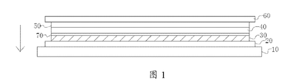
- FIG. 1 is a schematic structural diagram of a first embodiment of an organic electroluminescent device of the present application
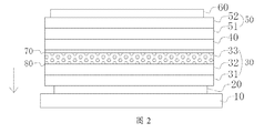
- FIG. 2 is a schematic diagram of a specific structure of a high-energy light sacrificial layer in a first embodiment of an organic electroluminescent device of the present application;
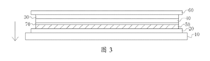
- FIG. 3 is a schematic structural diagram of a second embodiment of an organic electroluminescent device of the present application.
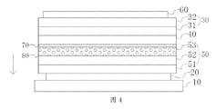
- FIG. 4 is a schematic diagram of a specific structure of a high-energy light sacrificial layer in a second embodiment of an organic electroluminescence device of the present application;
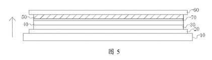
- FIG. 5 is a schematic structural diagram of a third embodiment of an organic electroluminescent device of the present application.
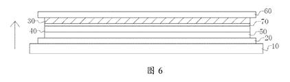
- FIG. 6 is a schematic structural diagram of a fourth embodiment of an organic electroluminescent device according to the present application.
- FIG. 7 is a schematic structural diagram of a fifth embodiment of an organic electroluminescent device according to the present application.
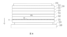
- FIG. 8 is a schematic structural diagram of a sixth embodiment of an organic electroluminescent device according to the present application.
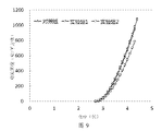
- FIG. 9 is an instantaneous current and voltage trend graph of the control group 1 and the experimental group 1 and the experimental group 2 in the present application.
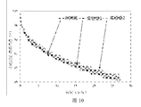
- FIG. 10 is a comparison diagram of device lifetimes of the control group 1 and the experimental group 1 and the experimental group 2 in the present application; FIG.
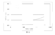
- 11 is a comparison chart of experimental results of the control group 2 and the experimental group 4 in the present application.
- Reference numerals in the figure 10, substrate; 20, first electrode; 30, hole transport functional layer; 60, second electrode; 40, light emitting layer; 50, electron transport functional layer; 32, hole transport layer HT; 31, Hole injection layer HI; 33, high energy light sacrificial layer; 52, electron injection layer EI; 51, electron transport layer ET; 70, first additional functional layer; 80, light absorbing material; 81, light absorbing material layer.
- FIG. 1 is a schematic structural diagram of a first embodiment of an organic electroluminescence device in this application.
- the organic electroluminescence device is an OLED device, which includes a substrate 10 and a first electrode 20 which are sequentially stacked.
- the layer HI 31, the hole transport layer HT32, and the hole blocking layer HBL, and the high-energy light sacrifice layer 33 is composed of a hole blocking layer HBL doped with a light absorbing material 80.
- the light absorbing material is a photoluminescent material, specifically a fluorescent material; in other embodiments, the light absorbing material may also be other photoluminescent material, such as a phosphorescent material or a quantum dot light emitting material (also called a quantum dot material) );
- the fluorescent material is a red fluorescent material.
- the fluorescent material may also be a green fluorescent material or a blue fluorescent material, such as C545T (2,3,6,7-Tetrahydro-1,1,7,7. , -Tetramethyl-1H, 5H, 11H-10- (2-benzothiazolyl) quinolizino [9,9a, 1gh] coumarin), AND (9,10-Di (naphth-2-yl) anthracene), DBP (Dibenzo ⁇ [ f, f ']-4,4', 7,7'-tetraphenyl ⁇ diindeno [1,2,3-cd: 1 ', 2', 3'-lm] perylene), Rubrene (5,6,11, 12-Tetrapheny lnaphthacene) and the like; the fluorescent material may be, for example, a thermally delayed fluorescent material such as 2PXZ-OXD (2,5-bis (4,5-bis (4,
- Quantum dot luminescent materials can be, for example, perovskite quantum dots.
- the most common quantum dots are II-VII (Cdse, Cds, Znse, Cds, Pbs, Pbse), III-VI (InP, InAs), or I-III- Semiconductor nanoparticles composed of Group VII (CuIns2, AgIns2).
- the energy gap of the photoluminescent material is higher than the energy gap of the material of the light emitting layer and lower than the energy gap of the doped host material of the high-energy light transmission layer; the photoluminescent material becomes excited after absorbing high-energy light When the state is converted from the excited state back to the ground state, energy is released in the form of light emission. This mechanism is called photoluminescence. Since photoluminescence absorbs high-energy light, the light emitted by the photoluminescent material is emitted by the photoluminescent material.
- the characteristics determine that the light emitted by the photoluminescent material after absorbing high-energy light is in the visible light band of light blue-green-yellow-red with a wavelength of 500-700nm, so the high-energy light sacrificial layer can also be called a color conversion layer;
- the light emitting band of most OLED devices is between 450nm and 700nm, and the energy gap of the photoluminescent material is lower than that of the light-emitting layer. Therefore, the light emitted by the OLED will not be affected by the photoluminescent material (color Conversion layer) absorption.
- the volume percentage of the photoluminescent material in the high-energy light sacrificial layer is 10%. In other embodiments, the volume percentage of the photoluminescent material in the high-energy light sacrificial layer is greater than or equal to 0.1 % Is other than 15%.
- a first additional functional layer 70 is provided between the high-energy light sacrificial layer 33 and the light-emitting layer 40 to avoid electroluminescence.
- the hole transporting functional layer 30 may be made of a material capable of realizing hole transport
- the electron transporting functional layer 50 may be made of a material capable of realizing electron transport.
- the high-energy light sacrificial layer may emit light under electric driving.
- a first additional functional layer 70 is placed between the high-energy light sacrificial layer and the light-emitting layer.
- the material has the same charge transport characteristics as the host material of the high-energy light sacrificial layer; in this way, it can ensure that there is only a single type of carrier (electron or hole) in the high-energy light sacrificial layer, and the effect of avoiding electroluminescence can be achieved.
- the concept of the same body material is the same charge transport characteristics; in this embodiment, since the light absorbing material is doped in the hole transport functional layer, the first additional functional layer 70 may be made of the hole transport functional material.
- the hole transport functional material can be different types of HBL, such as HBL1, HBL2, or HBL3 ...
- FIG. 3 a schematic structural diagram of a second embodiment of an organic electroluminescent device of the present application.
- the OLED is also a bottom-emission type in this embodiment, and the difference from the first embodiment is as follows:
- the electron-transporting functional layer 50 is formed between the light-emitting layer 40 and the first electrode 20.
- the high-energy light sacrifice layer is formed by doping a light-absorbing material in the electron-transporting functional layer 50.
- the first additional functional layer 70 is also Accordingly, it is provided between the electron-transporting functional layer 50 and the light-emitting layer 40.
- the electron transport function layer 50 is composed of an electron injection layer EI 51, an electron transport layer ET 52, and a hole blocking layer HBL53.
- a light absorbing material 80 is doped in the hole blocking layer 53, and the high-energy light sacrificial layer is The hole blocking layer HBL53 doped with the light absorbing material 80 is composed; the material of the first additional functional layer 70 is also HBL.
- FIG. 5 is a schematic structural diagram of a third embodiment of an organic electroluminescent device of the present application.
- the OLED is a top-emission type
- the electron transmission functional layer 50 is provided.
- the high-energy light sacrifice layer is formed by doping a light-absorbing material in the electron-transporting functional layer 50, and the first additional functional layer 70 is correspondingly disposed on the electron-transporting functional layer 50 and Between the light emitting layers 40.
- FIG. 6 a schematic structural diagram of a fourth embodiment of an organic electroluminescence device of the present application.
- the OLED in this embodiment is also a top-emission type.
- the difference is that in this implementation, In the example, the hole-transporting functional layer 30 is disposed between the light-emitting layer 40 and the second electrode 60; at this time, the high-energy light sacrifice layer is formed by doping a light-absorbing material in the hole-transporting functional layer 30, and the first additional functional layer 70 is correspondingly formed. Ground is provided between the hole-transporting functional layer 30 and the light-emitting layer 40.
- Embodiments 1 to 4 illustrate that the technical solution of the present application is not only applicable to OLED devices having a PIN (hole transport function layer-light-emitting layer-electron transport function layer) structure, but also applicable to NIP structures (electron transport function layer-light emitting device).
- Layer-hole transport functional layer) OLED devices are not only suitable for bottom-emitting OLED devices but also for top-emitting OLED devices.
- the light absorbing material 80 is separately set up to form a single light absorbing material layer 81, and the light absorbing material layer 81 is located between the light emitting layer and the hole blocking layer HBL.
- a light absorbing material layer 81 is disposed between the hole injection layer HI31 and the hole transport layer HT32.
- the light absorbing material layer 81 may be disposed between the hole blocking layer HBL and the hole transporting layer HT32. Therefore, the high-energy light sacrificial layer of the present application is defined as: layered or hole-transporting functional layer doped with light-absorbing material, layered or electron-transporting functional layer doped with light-absorbing material, light-absorbing material layer and its phase The layered superposition of the hole transport function layer adjacent to the light emitting layer or the layer of the light absorbing material layer and the electron transport function layer adjacent to the layer and the electron transport function layer adjacent to the light emitting layer.
- the light-absorbing material 80 in the first embodiment is replaced by a photoluminescent material with a colored light-absorbing material, specifically 2- (2'-fluorenyl 3 ', 5'-di-t-pentylphenyl ) Benzotriazole; in other embodiments, the colored light absorbing material may be, for example, salicylate, benzophenone, benzotriazole, substituted acrylonitrile, triazine, direct dye, basic At least one of a dye, an acid dye, a disperse dye, a reactive dye, a sulfur dye, a vat dye, and a cationic dye.
- a colored light-absorbing material specifically 2- (2'-fluorenyl 3 ', 5'-di-t-pentylphenyl ) Benzotriazole
- the colored light absorbing material may be, for example, salicylate, benzophenone, benzotriazole, substituted acrylonitrile, triazine, direct dye, basic At least one
- Direct dyes are, for example, diaminostilbene disulfonic acids, 4.4 ⁇ -diaminodiphenylureas, 4.4 ⁇ -diaminobenzoyl anilines, 4.4 ⁇ -diaminobenzene sulfanilides, diamino Heterocyclics and other types of dyes, such as 2- (2'-fluorenyl 3 ', 5'-di-t-pentylphenyl) benzotriazole, 2-fluorenyl-4-n-octyloxydiphenyl Methyl ketone; acid dyes such as bromine derivatives; colored light-absorbing materials are colored dyes, which can be defined as ultraviolet / near-ultraviolet / blue light absorbers, because the main absorption band is in the ultraviolet / near-ultraviolet / dark blue light band, A green translucent / yellow translucent / red translucent visual appearance will appear in the color.
- Colored light-absorbing materials can absorb most of the short-wave high-energy rays (greater than 60%) below 450nm, and the range is 450-500nm.
- the percentage of the blue light band that is absorbed is between 30% and 60%, and for the range of 500nm-750nm (this band is also the light emitting band of the light-emitting layer), the transmittance of the optical band is above 80%, that is, the ratio of absorption Below 20%.
- the volume percentage of the colored light absorbing material in the high-energy light sacrificial layer is 5%, and in other embodiments, the volume percentage of the colored light absorbing material in the high-energy light sacrificial layer Other values may be 0.1% or more and 10% or less.
- an exciton quenching material is further added to the high-energy light sacrifice layer in the first embodiment.
- the exciton quenching material is used as a second additional functional material and is incorporated in hole transport.
- the functional layer it is used to improve the charge transport capability;
- the exciton quenching material may be, for example, an alkali metal group ionic compound, a metal salt, a metal oxide, a metal, a high electron affinity organic material or an organic metal complex, carbon At least one of the materials, the exciton quenching material may also be other materials having an exciton quenching function.
- the exciton quenching material may form a single layer.
- this mechanism may also cause the host light-absorbing material (hole / electron transfer or injection material) to accelerate cracking and reduce performance, so at least one kind is added to the high-energy light sacrificial layer
- the exciton quenching material quenches the luminescent material in the excited state in microseconds (us) or less, which helps to shorten the time that all luminescent materials are in the unstable excited state, that is, it increases the luminescent material. The lifetime of the organic electroluminescent device is thus improved.
- the exciton quenching material may be at least one of an alkali metal group ionic compound, a metal salt, a metal oxide, a metal, an organic material with a high electron affinity, an organic metal complex, or a carbon material.
- the alkali metal group ionic compound is a salt.
- the metal oxide may be MoO 3 molybdenum oxide, WO 3 tungsten oxide, Al 2 O 3 alumina; the metal material may be Al aluminum, Ag silver, Au gold, Li lithium, Cs cesium, etc .; Compounds such as F4-TCNQ, F16-CuPc, HAT-CN, Pentacene, NDP-9, etc .; carbon materials such as C60, Graphene, carbon nanotubes, fullerene, etc .; high electron affinity organic materials such as It is F4-TCNQ, Liq (8-hydroxy-quinolinato lithium), the chemical formula of F4-TCNQ is tetracyanodimethyl p-benzoquinone,
- the exciton quenching material and the host material of the high-energy light sacrificial layer satisfy the following energy requirements: the highest occupied molecular orbital of the host material and the lowest unoccupied molecules of the organic material and organometallic complex
- the orbital gap is less than or equal to 0.6 eV; the work function of the alkali metal group ionic compound, metal salt, metal oxide, metal, and carbon material is lower than the minimum unoccupied molecular orbital of the colored light absorbing material by more than 0.2 eV.
- the above-mentioned exciton quenching material and the host material of the high-energy light sacrificial layer will form a so-called charge exchange complex or exciplex after satisfying the above-mentioned energy; the change of the above state can change the host material Optical gaps, such as high electron affinity organic materials or organometallic complexes (F4-TCNQ, F16-CuPc, HAT-CN, Pentacene, NDP-9, etc.) and hole transport materials NPB (N, N'-Bis ( naphthalen-1-yl) -N, N'-bis (phenyl) -benzidine), m-MTDATA (4,4 ', 4 "-Tris (N-3-methylphenyl-N-phenyl-amino) triphenylamine) It has the effect of adjusting the optical energy gap; reducing the energy gap of the doped host material makes the material state more stable, and the hole transport material NPB is the host material of the hole transport functional layer.
- an exciton quenching material is further added to the high-energy light sacrifice layer in Embodiment 7.
- the exciton quenching material is used as a second additional functional material, which is incorporated in hole transport In the functional layer, it is used to improve the charge transport capability; the choice of the exciton quenching material can be the same as that in the eighth embodiment.
- the volume percentage of the exciton quenching material in the high-energy light sacrificial layer is 10%.
- the volume of the exciton quenching material in the high-energy light sacrificial layer is 10%. The percentage may be other values from 2% to 15%.
- the light absorbing material 80 in the first embodiment is replaced by a photoluminescence material with an exciton quenching material; the choice of the exciton quenching material is the same as that in the eighth embodiment.
- the volume percentage of the exciton quenching material in the high-energy light sacrificial layer is 8%. In other embodiments, the volume of the exciton quenching material in the high-energy light sacrificial layer is 8%. The percentage may be other values from 2% to 15%.
- the light absorbing material in this application may be at least one of a photoluminescent material, a colored light absorbing material, or an exciton quenching material.
- the "light absorbing material” is defined as capable of absorbing high-energy light.
- the volume percentage of the light-absorbing material in the high-energy light sacrificial layer is greater than or equal to 0.1% and less than or equal to 30%.
- this embodiment also provides an embodiment of a method for preparing an organic electroluminescent device, including the following steps:
- the vacuum electrodeposition, wet process, inkjet printing technology, spin coating, and slit coating are used to sequentially form a first electrode, an electron transporting function layer or a hole transporting function layer, and emit light on the substrate.
- the high-energy light sacrificial layer contains a light-absorbing material capable of absorbing high-energy light
- the first additional functional layer contains a material to avoid electroluminescence.
- the high-energy light sacrificial layer of the doped light-absorbing material in the OLED device can achieve the effect of uniform mixing by means of vacuum thermal evaporation; the light-absorbing material can also be dissolved in a solvent by a wet process, and the polymer semiconductor material or Dissolve small-molecule semiconductor materials (the host material of the electron transport function layer or the hole transport function layer) and mix them uniformly. They are evenly distributed on the substrate by thin film processes such as inkjet printing technology, spin coating, and slit coating.
- the solvent is then evacuated by means of vacuum volatilization and heating to volatilize the solvent to form a dense and dry high-energy light sacrificial layer.
- the first additional functional layer 70 is made of the main material of the high-energy light sacrifice layer or a material with similar functions.
- the concept of the same main material is the same charge transfer characteristics:
- the material of the first additional functional layer 70 is capable of realizing the hole-transporting function.
- the material can be, for example, different types of HT, such as HT1, HT2, or HT3 ...;
- the material of the first additional functional layer 70 is capable of hole injection. Functional materials are sufficient;
- the material of the first additional functional layer 70 may be a material capable of realizing the electron-blocking function.
- the material of the first additional functional layer 70 may be a material capable of realizing the electron injection function
- the material of the first additional functional layer 70 may be a material capable of realizing the electron-transporting function
- the material of the first additional functional layer 70 is a material capable of realizing the hole blocking function.
- the high-energy light sacrifice layer when the high-energy light sacrifice layer is disposed on the hole-transporting functional layer, it can and is not limited to the situations described in Table 1 below:
- experimental group 1 and experimental group 2 are composition descriptions of each layer of the organic layer of the OLED panel in the examples provided in the present application; control group 1 is the component of the OLED panel in the prior art of the present application. The composition of each layer of the organic layer is explained.
- Experiment group 2 HI / HT (17nm) / Yellow dopant (3nm) / HT (20nm) / Light-emitting layer / ET
- the experimental group 1 is based on the control group 1, and a yellow fluorescent material (Yellow dopant) is mixed in the HT layer of the control group 1.
- the experimental group 2 is provided with a 3 nm thick yellow layer on the surface of the HT layer in the control group 1. Fluorescent material layer; HT (20 nm) adjacent to the light emitting layer in the experimental group 1 and the experimental group 2 was used as the first additional functional layer. As shown in FIG. 9 and FIG. 10 and Table 3, after the high-energy light sacrifice layer is provided, the electrical parameters of the screen are relatively close to those of the control group 1, but the life of the screen is significantly improved.
- the materials of the first additional functional layer 70 of the experimental group 1 and the experimental group 2 are both HT and the thickness are both 20 nm. In other embodiments, the thickness of the first additional functional layer may also be Other values are 10nm or more and 100nm or less.
- FIG. 10 is a comparison chart of the device lifetime of the control group 1 and the experimental group 1 and the experimental group 2. This figure is a case of lighting for a long time under a specific brightness condition, and measuring the brightness reduction at different times.
- the ordinate in FIG. 10 is Brightness value.
- the brightness in experimental group 1 and experimental group 2 is brighter than that in control group 1, which indicates that the brightness attenuation of experimental group 1 and experimental group 2 is better than the control.
- Group 1 is slower, which means that experimental group 1 and experimental group 2 have a longer service life than control group 1.
- the yellow fluorescent material may be replaced with another photoluminescent material.
- experimental group 1 and experimental group 3 are component descriptions of each layer of the organic layer of the OLED panel in the example provided by the present application.
- control group 2 is a composition description of each layer of the organic layer of the OLED screen in the prior art
- experimental group 4 is a composition of each layer of the organic layer of the OLED screen in an embodiment of the present application Instructions.
- the high-energy light sacrificial layer structure is NPB: F4-TCNQ: Rubrene, and the three are doped according to an optimized ratio; Rubrene is a fluorescent dye.
- the two screens in the control group 2 and the experimental group 4 were irradiated with simulated sunlight for 1300 hours, and the photoelectric characteristics were measured every 48 hours.
- the experimental results indicate that the experimental group 4 was photoelectrically The characteristics are stable, while the voltage of the same current density in the control group 2 increased by 1.7V due to the influence of irradiation, and the area unevenness phenomenon appeared.
- the effect of the high-energy light sacrificial layer was obvious.
- the experimental group 5 to experimental group 9 of this control experiment respectively correspond to the examples provided in this application.
- the device structure of the OLED panel of each example is: ITO-glass / NPB: Rubrene: F4-TCNQ (x nm) / NPB (250-x nm) / ET (15nm) / EML / ET / Al where x is the thickness of the high-energy light sacrificial layer.
- ITO-glass is the first electrode
- NPB Rubrene: F4-TCNQ (xnm) / NPB (250-xnm) is a hole transport functional layer doped with fluorescent dye-Rubrene and exciton quenching material-F4-TCNQ ET (15nm) is the first additional functional layer
- EML is the light-emitting layer
- ET is the electron transport functional layer
- Al is the second electrode
- the numerical values of x corresponding to the above experimental group 5 to experimental group 9 are 10nm, 30nm, 100nm, 200nm, 250nm.
- the main material of the high energy light sacrificial layer in the above experimental group 5 to experimental group 9 is the hole transport material NPB, the light absorbing material uses a fluorescent dye Rubrene (concentration of 2%), and the exciton quenching material uses F4-TCNQ (concentration is 8%).
- the OLED screens of the above experimental group 5 to experimental group 9 were stored under simulated sunlight for 1000 hours under 1000W / m ⁇ 2 (with a wavelength of 300nm-400nm and an ultraviolet intensity of 30W / m ⁇ 2), and the driving voltage was the same under the same current. Results The results are shown in Table 7 below:
- the above experimental results show that the thickness of the high-energy light sacrificial layer is more than 30nm, which has an improvement effect on the photoelectric performance of the OLED screen.
- This experiment is mainly used to test the effect of different concentrations of exciton quenching materials on the photoelectric properties of OLED screens.
- experimental group 10 to experimental group 13 are composition descriptions of each layer of the organic layer of the OLED panel in the examples provided in the present application.
- the following prime represents the first additional functional layer; Table 9 corresponds to this control.
- the exciton quenching material generally has the function of improving the charge transporting ability.
- the exciton quenching material in this experimental group is generally used to improve the charge transporting ability.
- the doping concentration of the material used to improve the charge transporting ability Generally, the charge transfer ability can be significantly improved at about 2%.
- the material that further enhances the charge transport ability that is, the concentration of the exciton quenching material.
- the concentration is increased to 2-10%, the photoelectric transmission performance of the OLED panel is affected by 10%.
- the charge transport capacity is improved by at least two orders of magnitude; and in the above experimental group 10 to experimental group 13, the hole transport material m-TDATA with an optical energy gap of about 2.91 electron volts is used to mix the high electron affinity material F4- TCNQ obtains a hole-transporting functional layer with an F4-TCNQ concentration of about 2-10%; when the hole-transporting functional layer has an m-TDATA: F4-TCNQ (20%, 150nm) structure, its optical energy gap is calculated to decrease from 2.91 To 2.55 electron volts, the mold layer was visually observed to change from near transparent to light yellow.
- the characteristics under irradiation were compared.
- the screen body was at 1000 W / m ⁇ 2 (the ultraviolet intensity at a wavelength of 300-400 nm was 30 W / m ⁇ 2).
- the stability of the screen is significantly improved, and the voltage can basically achieve a significant improvement without change in the measurement time. That is to say, this experimental group shows that doping a high concentration of exciton quenching material (charge transporting property improving material) alone in the hole transport function layer or the electron transport function layer can not only play the role of exciton quenching, but also To the role of charge enhancement, and the excess light absorbing material can further play a role in blocking high-energy light.
- charge transporting property improving material charge transporting property improving material
- the doped exciton quenching material makes a large amount of charge exist in the doped electron transport function layer and the hole transport function layer, while the light emitting layer theoretically has a large number of excitons.
- the exciton dominates the luminous efficiency and luminescence characteristics.
- the exciton It is easy to interact with the charge, this interaction can easily cause the exciton to quench; the exciton easily interacts with the charge, but the formation of the exciton also starts from the charge (holes and electrons enter the light-emitting layer respectively, and electrons and holes recombine
- the excited state before light emission is called an exciton)
- the first additional functional layer has the same carrier transport characteristics as the electron transport functional layer or hole transport functional layer, but the characteristics are worse than the doped layer, which can make the charge Deposition occurs at the contact surface between the high-energy light sacrificial layer and the first additional functional layer, and at the same time can supply the charges required for the light-emitting layer to generate excitons, because the separation of the first additional functional layer can effectively reduce the interaction between excitons and charges Quenching effect caused by action.
- the first additional functional layer designed in the above embodiments of the present application may also be called a protective layer.
- the charge can be reduced. It interacts with excitons; it can also limit the exciton staying in the light-emitting layer, avoiding the occurrence of quenching phenomenon.
- experimental group 14 and experimental group 15 are composition descriptions of each layer of the organic layer of the OLED panel in the examples of the present application; control group 1 is an organic layer of the OLED panel in the prior art of the present application. The composition of each layer of the layer is explained.
- the experimental group 14 is based on the control group 1 and is mixed with a colored light absorbing material (2- (2'-fluorenyl 3 ', 5'-di-t-pentylphenyl) benzotris) in the HT layer of the control group 1.
- Azole a colored light absorbing material
- experimental group 15 is a layer of colored light-absorbing material with a thickness of 3 nm on the surface of the HT layer in control group 1; HT (20 nm) adjacent to the light-emitting layer in experimental group 14 and experimental group 15 is the first Additional functional layers.
- Table 11 after the high-energy light sacrificial layer is set, the electrical parameters of the screen are relatively close to those of the control group 1, but the life of the screen is significantly improved.
- the experimental group 14 and the experimental group 16 are composition descriptions of each layer of the organic layer of the OLED panel in the examples of the present application.
- the experimental results in Table 13 above indicate that the experimental group 16 containing p-type doping (F4-TCNQ) containing exciton quenching material has a significantly lower operating voltage than the experimental group 14 at the same brightness, showing a better performance.
- the photoluminescence phenomenon can be observed in the high-energy light sacrifice layer and the light-emitting layer in the experimental group 14, but not in the experimental group 16
- the photoluminescence of the luminescent material in the light emitting layer of the device shows that most of the ultraviolet light is absorbed and quenched by the high energy light sacrificial layer. Therefore, the experimental group 16 is more effective than the experimental group 14 in protecting the light emitting layer from the impact of high energy light.
- the photoluminescent material and the colored light absorbing material can also be used in the high-energy light sacrificial layer at the same time, for example, HT: 2- (2'-fluorenyl 3 ', 5'- Add difluoropentylphenyl) benzotriazole (20nm) layer with fluorescent dye, or HT: 2- (2'-fluorenyl 3 ', 5'-dipentylphenyl) in experimental group 16 Benzotriazole (20 nm) was added with a phosphorescent dye.
- the design principles of the high-energy light sacrificial layer provided in the above embodiments are applicable to various forms of OLED light-emitting devices, including basic single-light-emitting layer originals, stacked devices, inverted devices, and top-emitting devices.
- a hole injection material commonly used in the industry can be used to co-evaporate with the commonly used commercial material NDP-9 and the fluorescent material Rubrene to complete a high-energy light sacrificial layer at the hole-transport side.
- the high-energy light sacrificial layer uses absorption radiation to block high-energy light. And ways to improve hole transport capabilities;
- the high-energy light sacrificial layer uses Bphen and silver complexes to improve the electron transmission characteristics, and some silver atoms Does not react with organic molecules, has the ability to absorb light irradiation.
Landscapes
- Physics & Mathematics (AREA)
- Optics & Photonics (AREA)
- Electroluminescent Light Sources (AREA)
Abstract
本申请公开了一种有机电致发光器件,包括依次设置的基板、第一电极、有机层、第二电极和封装结构;有机层包括发光层、位于发光层两侧的空穴传输功能层和电子传输功能层;发光器件的出光面对应的电极与发光层之间设置有高能量光线牺牲层,高能量光线牺牲层内含有吸光材料;高能量光线牺牲层与发光层之间设置有用于避免电致发光的第一附加功能层。本申请通过在发光器件内部设置高能量光线牺牲层,从本质上使得OLED器件具有对抗高能量光线的能力,从而大幅度提升OLED相关产品的可靠性与使用寿命,也能增加应用空间。
Description
本申请一般涉及照明领域,具体涉及OLED照明领域,尤其涉及一种有机电致发光器件。
OLED(Organic Light Emitting Diode,有机发光二极管)是指有机半导体材料和发光材料在电场驱动下,通过载流子注入和复合导致发光的现象。其原理是用透明/半透明金属/金属氧化物电极和金属/金属氧化物电极分别作为器件的阳极和阴极,在外部电场驱动下,载子(电子和空穴)分别从阴极和阳极注入到电子和空穴传输功能层,电子和空穴分别经过电子和空穴传输功能层传递到发光层,并在发光材料中形成激子(exciton),激子中受限的电子-空穴复合后消失,能量以可见光的形式辐射(发光波长受限于发光材料特性)。辐射光可从透明/半透明电极侧观察到。此发光原理被大量应用在照明与显示屏上。
但多数有机材料对高能量光线敏感,一般环境中主要存在的高能量光线为发光能量落在2.8-4.1电子伏特的光线,OLED器件中部分材料有可能因为环境中的高能量光线进入而导致衰减,衰减的规则为:高能量光线的照度和照射时间量值的乘积接近一固定值。OLED照明应用上,把衰减达到原始亮度的某个比例会定义成OLED照明的寿命,如果OLED器件应用上(如车用或航空照明)会大量被高能量光线照射,则其中的高能量光线会加速屏体的老化,缩短其寿命。
针对上述问题,业界通常的做法有:在屏体外部制备能够阻挡高能量光线的组件,减少高能量光进入OLED器件,缓解其对器件的劣化,比如使用外部壳罩、抗紫外薄膜、反射层等,从而增加OLED屏体使用寿命。但这些做法无一例外都会引入新的材料或组件,增加工艺和成本,增大产品体积和重量,甚至带来新的产品隐患。
发明内容
鉴于现有技术中的上述缺陷或不足,期望提供一种可以从本质上提高OLED器件本身的抗高能量光线辐照能力且不影响外观设计的有机电致发光器件。
第一方面本申请提供一种有机电致发光器件,包括依次叠加设置的基板、第一电极、有机层、第二电极和封装结构;所述有机电致发光器件的出光面位于第一电极或第二电极一侧;所述有机层包括发光层、位于发光层两侧的空穴传输功能层和电子传输功能层;发光器件的出光面所在的第一电极或第二电极与发光层之间设置有高能量光线牺牲层,所述高能量光线牺牲层与所述发光层之间设置有用于避免电致发光的第一附加功能层。
根据本申请实施例提供的技术方案,所述高能量光线牺牲层由空穴传输功能层或电子传输功能层作为掺杂主体掺杂吸光材料。
根据本申请实施例提供的技术方案,所述高能量光线牺牲层包括空穴传输功能层/电子传输功能层及位于空穴传输功能层/电子传输功能层内或表面的吸光材料层;所述吸光材料层由吸光材料形成。
根据本申请实施例提供的技术方案,所述吸光材料包括光致发光材料、有色吸光材料和激子淬灭材料中的至少一种。
根据本申请实施例提供的技术方案,所述光致发光材料的吸收光谱最低能量起始位置高于所述发光层材料的发光光谱的最高能量主峰能量位置且低于所述高能量光线传输层的掺杂主体材料的光学能隙。
根据本申请实施例提供的技术方案,所述光致发光材料为荧光材料、磷光材料或量子点发光材料中的一种或两种。
根据本申请实施例提供的技术方案,所述吸光材料在所述高能量光线牺牲层中的体积百分比大于等于0.1%小于等于30%。
根据本申请实施例提供的技术方案,所述光致发光材料在所述在所述高能量光线牺牲层中的体积百分比大于等于0.1%小于等于15%。
根据本申请实施例提供的技术方案,所述有色吸光材料在所述在所述高能量光线牺牲层中的体积百分比大于等于0.1%小于等于10%。
根据本申请实施例提供的技术方案,所述激子淬灭材料在所述在所述高能量光线牺牲层中的体积百分比大于等于2%小于等于15%。
根据本申请实施例提供的技术方案,所述有色吸光材料为水杨酸酯类、二苯甲酮类、苯并三唑类、取代丙烯腈类、三嗪类,直接染料、碱性染料、酸性染料、分散染料、活性染料、硫化染料、还原染料、阳离子染料中的至少一种。
根据本申请实施例提供的技术方案,所述有色吸光材料为2-(2’-羫基3’,5’-二特戊基苯基)苯并三唑,2-羫基-4-正辛氧基二苯甲酮的任意一种或两种。
根据本申请实施例提供的技术方案,所述激子淬灭材料包括碱金属族离子化合物、金属盐类、金属氧化物、金属、高电子亲和力有机材料或有机金属错合物、碳材中的至少一种。
根据本申请实施例提供的技术方案,所述激子淬灭材料与所述高能量光线牺牲层的主体材料满足以下能量要求:所述有机材料及有机金属错合物最低未占分子轨道的差距小于等于0.6eV;所述碱金属族离子化合物、金属盐类、金属氧化物、金属、碳材的功函数低于所述有色吸光材料的最低未占分子轨道0.2eV以上。
根据本申请实施例提供的技术方案,所述第一附加功能层的材料与所述高能量光线牺牲层的主体材料具有相同的电荷传输特性。
根据本申请实施例提供的技术方案,所述第一附加功能层的厚度大于等于10nm小于等于100nm。
根据本申请实施例提供的技术方案,所述高能量光线牺牲层的厚度大于等于30nm小于等于250nm。
第二方面,本申请提供一种有机电致发光器件的制备方法,包括以下步骤:
采用真空热蒸镀、湿法工艺、喷墨印刷技术、旋转涂布、狭缝涂布中的任意一种方式在基板上依次形成第一电极、高能量光线牺牲层、第一附加功能层、发光层、电子传输功能层或空穴传输功能层、第二电极;所述发光层的出光面位于所述第一电极一侧;
或,
采用真空热蒸镀、湿法工艺、喷墨印刷技术、旋转涂布、狭缝涂布中的任意一种方式在基板上依次形成第一电极、电子传输功能层或空穴传输功能层、发光层、第一附加功能层、高能量光线牺牲层、第二电极;所述发光层的出光面位于所述第二电极一侧;
所述高能量光线牺牲层含有可吸收高能量光线的吸光材料;
所述第一附加功能层中含有避免电致发光的材料。
本申请通过在有机电致发光器件(OLED器件)的特定位置-发光层与出光面的电极层之间设置高能量光线牺牲层,从本质上使得OLED器件自身具有对抗高能量光线的能力,从而大幅度提升OLED相关产品的可靠性与使用寿命,也能增加应用空间。
根据本申请实施例提供的技术方案,高能量光线牺牲层设置在空穴传输功能层或电子传输功能层中,尤其高能量光线牺牲层为空穴传输功能层或电子传输功能层中掺杂吸光材料时,吸光材料具有屏蔽高能量光线的作用,该方案使得本申请的技术方案可在不影响原有OLED器件结构和生产工艺的前提下提高OLED器件的吸收高能量光线的能力;吸光材料采用光致发光材料、有色吸光材料、激子淬灭材料中的至少一种,使得高能量光线牺牲层对外来高能量光辐照吸收并转换成低能量光线或能量转化为声子消散;可以显著改善高能量光线对OLED屏体造成发光不均匀的影响,也可以减缓长时间高能光线照射后OLED屏体电压上升的情况。
根据本申请实施例提供的技术方案,高能量光线牺牲层设置在空穴传输功能层或电子传输功能层中或在空穴传输功能层或电子传输功能层表面形成一层吸光材料层,吸光材料层由吸光材料组成,该方案工艺简单,易于制备。
本申请高能量光线牺牲层中的吸光材料主要选自光致发光材料、有色吸光材料、激子淬灭材料中的至少一种,选材通用方便,对原OLED器件效能的影响在15%以下,但该层对高能量光线的吸收,可以减缓长时间高能光线照射后OLED屏体电压的上升速度,使得高能量光线照射后OLED屏体的电压上升的至高点更低,因OLED屏衰减效果在光电性能下降上表征为亮度下降和电压上升,因此减缓电压的 上升速度和电压上升的最高点就等于可以增加屏体使用寿命,试验表明本申请的技术方案使得屏体的使用寿命提高至少30%。
本申请在高能量光线牺牲层与发光层之间设置第一附加功能层可有效避免电致发光的出现,尤其当附加功能层采用高能量光线牺牲层主体材料制备时,效果更佳,工艺更简单。
通过阅读参照以下附图所作的对非限制性实施例所作的详细描述,本申请的其它特征、目的和优点将会变得更明显:
图1是本申请有机电致发光器件第一种实施例的结构示意图;
图2是本申请有机电致发光器件第一种实施例中高能量光线牺牲层的具体结构示意图;
图3是本申请有机电致发光器件第二种实施例的结构示意图;
图4是本申请有机电致发光器件第二种实施例中高能量光线牺牲层的具体结构示意图;
图5是本申请有机电致发光器件第三种实施例的结构示意图;
图6是本申请有机电致发光器件第四种实施例的结构示意图;
图7是本申请有机电致发光器件第五种实施例的结构示意图;
图8是本申请有机电致发光器件第六种实施例的结构示意图;
图9是本申请中对照组1与实验组1和实验组2的瞬时电流和电压趋势图;
图10是本申请中对照组1与实验组1和实验组2的器件寿命的对比图;
图11为本申请中对照组2和实验组4的实验结果对比图;
图中标号:10、基板;20、第一电极;30、空穴传输功能层;60、第二电极;40、发光层;50、电子传输功能层;32、空穴传输层HT;31、空穴注入层HI;33、高能量光线牺牲层;52、电子注入层EI;51、电子传输层ET;70、第一附加功能层;80、吸光材料;81、吸光材料层。
下面结合附图和实施例对本申请作进一步的详细说明。可以理解 的是,此处所描述的具体实施例仅仅用于解释相关发明,而非对该发明的限定。另外还需要说明的是,为了便于描述,附图中仅示出了与发明相关的部分。
需要说明的是,在不冲突的情况下,本申请中的实施例及实施例中的特征可以相互组合。下面将参考附图并结合实施例来详细说明本申请。
实施例一
请参考图1为本申请一种有机电致发光器件第一种实施例的结构示意图,在本实施例中,有机电致发光器件为OLED器件,包括依次叠加设置的基板10、第一电极20、空穴传输功能层30、发光层40、电子传输功能层50、第二电极60和封装结构(图中未画出);所述空穴传输功能层30、发光层40和电子传输功能层50形成OLED器件的有机层;所述有机电致发光器件的出光面在第一电极20一侧,第一电极20与发光层40之间设置有高能量光线牺牲层(设置在图中画斜杆的层内),高能量光线牺牲层由空穴传输功能层30作为掺杂主体掺杂吸光材料形成;如图2所示,在本实施例中,空穴传输功能层30包括空穴注入层HI 31、空穴传输层HT32和空穴阻挡层HBL,高能量光线牺牲层33由掺杂有吸光材料80的空穴阻挡层HBL组成。
在本实施例中,吸光材料为光致发光材料,具体为荧光材料;在其他实施例中,吸光材料也可以是其他光致发光材料,例如磷光材料或量子点发光材料(也叫量子点材料);
在本实施例中荧光材料为红色荧光材料,在其他实施例中荧光材料也可以是绿荧光材料或者蓝荧光材料,例如C545T(2,3,6,7-Tetrahydro-1,1,7,7,-tetramethyl-1H,5H,11H-10-(2-benzothiazolyl)quinolizino[9,9a,1gh]coumarin)、AND(9,10-Di(naphth-2-yl)anthracene)、DBP(Dibenzo{[f,f']-4,4',7,7'-tetraphenyl}diindeno[1,2,3-cd:1',2',3'-lm]perylene)、Rubrene(5,6,11,12-Tetrapheny lnaphthacene)等;荧光材料例如可以优选为热延迟荧光材料,例如2PXZ-OXD(2,5-bis(4-(10H-phenoxazin-10-yl)phenyl)-1,3,4-oxadiazole);磷光材料例如可以是Ir(btp)2(acac)(Bis(2- benzo[b]thiophen-2-yl-pyridine)(acetylacetonate)iridium(III))、Ir(mppy)3(Tris[2-(p-tolyl)pyridine]iridium(III))、FIrPic(Bis(3,5-difluoro-2-(2-pyridyl)phenyl-(2-carboxypyridyl)iridium(III))。
量子点发光材料例如可以是钙钛矿量子点,最常见量子点由II-VII族(Cdse,Cds,Znse,Cds,Pbs,Pbse)、III-VI族(InP、InAs)或I-III-VII族(CuIns2,AgIns2)组成的半导体纳米颗粒。
上述光致发光材料的能隙高于所述发光层材料能隙且低于所述高能量光线传输层的掺杂主体材料的能隙;上述光致发光材料在吸收高能量光线后会成为激发状态,从激发态转换回基态的时候,会以发光形式释放能量,此机制称为光致发光,由于光致发光是吸收高能量光线,光致发光材料发出的光线由该光致发光材料的特性决定,上述光致发光材料吸收高能量光线后释放的光线为波长介于500-700nm的浅蓝-绿-黄-红的可见光波段,因此高能量光线牺牲层也可以称为色转换层;多数OLED器件发光波段介于450nm-700nm的可光波段;而由于光致发光材料的能隙低于发光层材料的能隙,因此OLED所发出的光线是不会被该光致发光材料(色转换层)吸收。
所述光致发光材料在所述高能量光线牺牲层中的体积百分比为10%,在其他实施例中,所述光致发光材料在所述高能量光线牺牲层中的体积百分比为大于等于0.1%小于等于15%中的其他数值。
所述高能量光线牺牲层33与所述发光层40之间设置有用于避免电致发光的第一附加功能层70。上述空穴传输功能层30由能实现空穴传输的材料制成即可,上述电子传输功能层50由能实现电子传输的材料制成即可。
高能量光线牺牲层在电驱动下有可能会发光,为了避免这种情况出现,在高能量光线牺牲层与发光层之间放置有第一附加功能层70,所述第一附加功能层70的材料与所述高能量光线牺牲层的主体材料具有相同的电荷传输特性;如此可保证高能量光线牺牲层内只有单一种类载子(电子或空穴),可以达到避免电致发光的效果。
主体材质相同的概念为,具有相同的电荷传输特性;在本实施例 中,由于吸光材料掺杂在空穴传输功能层中,所以第一附加功能层70采用空穴传输功能材料制成即可,例如可以是不同类型的HBL,例如HBL1、HBL2、或HBL3……。
实施例二
请参考图3为本申请一种有机电致发光器件第二种实施例的结构示意图,和实施例一一样,在本实施例中OLED也是底面发光型的,和实施例一的区别为:本实施例中,发光层40和第一电极20之间为电子传输功能层50,此时高能量光线牺牲层即为电子传输功能层50中掺杂吸光材料形成,第一附加功能层70也相应地设置在电子传输功能层50和发光层40之间。
电子传输功能层50由电子注入层EI 51、电子传输层ET 52和空穴阻挡层HBL53组成;如图4所示,吸光材料80掺杂在空穴阻挡层53中,高能量光线牺牲层为掺杂有吸光材料80的空穴阻挡层HBL53组成;第一附加功能层70的材料也为HBL。
实施例三
请参考图5为本申请一种有机电致发光器件第三种实施例的结构示意图,和实施例二区别的是,在本实施例中OLED为顶面发光型的,电子传输功能层50设置在发光层40和第二电极60之间;此时高能量光线牺牲层即为电子传输功能层50中掺杂吸光材料形成,第一附加功能层70也相应地设置在电子传输功能层50和发光层40之间。
实施例四
请参考图6为本申请一种有机电致发光器件第四种实施例的结构示意图,和实施例三一样,本实施例中的OLED也是顶面发光型的,区别的是,在本实施例中空穴传输功能层30设置在发光层40和第二电极60之间;此时高能量光线牺牲层即为空穴传输功能层30中掺杂吸光材料形成,第一附加功能层70也相应地设置在空穴传输功能层30和发光层40之间。
上述实施例一至实施例四说明,本申请的技术方案不仅适用于PIN(空穴传输功能层-发光层-电子传输功能层)结构的OLED器件,也适用于NIP结构(电子传输功能层-发光层-空穴传输功能层)的 OLED器件,不仅适用于底面发光型的OLED器件,还适用于顶面发光型的OLED器件。
实施例五
如图7所示,在实施例一的基础上,将吸光材料80单独设立出来形成单独的一层吸光材料层81,且吸光材料层81位于发光层与空穴阻挡层HBL之间。
实施例六
如图8所示,在实施例五的基础上,在本实施例中,将吸光材料层81设置在空穴注入层HI31和空穴传输层HT32之间。
在其他实施例中,吸光材料层81也可以设置在空穴阻挡层HBL与空穴传输层HT32之间。因此本申请的高能量光线牺牲层的定义为:掺杂有吸光材料的空穴传输功能层的分层或,掺杂有吸光材料的电子传输功能层的分层或,吸光材料层及与其相邻的且靠近发光层一侧的空穴传输功能层的分层的叠加层或,吸光材料层及和其相邻的且靠近发光层一侧的电子传输功能层的分层叠加层。
实施例七
在实施例一的基础上,将实施例一中的吸光材料80由光致发光材料替换为有色吸光材料,具体为2-(2’-羫基3’,5’-二特戊基苯基)苯并三唑;在其他实施例中,有色吸光材料例如可以是水杨酸酯类、二苯甲酮类、苯并三唑类、取代丙烯腈类、三嗪类、直接染料、碱性染料、酸性染料、分散染料、活性染料、硫化染料、还原染料、阳离子染料中的至少一种。
直接染料例如为二氨基二苯乙烯二磺酸类、4.4`-二氨基二苯脲类、4.4`-二氨基苯甲酰替苯胺类、4.4`-二氨基苯磺酰替苯胺类、二氨基杂环类等类型的染料,具体例如为2-(2’-羫基3’,5’-二特戊基苯基)苯并三唑,2-羫基-4-正辛氧基二苯甲酮;酸性染料例如为溴氨酸衍生物等;有色吸光材料为有色染料,可以被定义为紫外线/近紫外/蓝光吸收剂,因为主要吸收波段落于紫外/近紫外/深蓝光波段,因此在颜色上会出现绿色半透明状/黄色半透明状/红色半透明状的视觉外观,有色吸光材料可以让450nm以下波短高能光线大部分(大于60%)被吸收,而界于 450-500nm的蓝光波段部分被吸收的比例介于30%-60%,而对于500nm-750nm(该波段也为发光层的发光的波段)的区间光波段穿透度在80%以上,即被吸收的比例在20%以下。
优选地,在本实施例中,有色吸光材料在所述高能量光线牺牲层中的体积百分比为5%,在其他实施例中所述有色吸光材料在所述高能量光线牺牲层中的体积百分比也可以是大于等于0.1%小于等于10%的其他数值。
实施例八
在实施例一的基础上,在实施例一中的高能量光线牺牲层中进一步加入包括激子淬灭材料,此时激子淬灭材料用作第二附加功能材料,掺入在空穴传输功能层中,用于提升电荷传输能力;所述激子淬灭材料例如可以是碱金属族离子化合物、金属盐类、金属氧化物、金属、高电子亲和力有机材料或有机金属错合物、碳材中的至少一种,所述激子淬灭材料也可以是其他具有激子淬灭功能的材料。
在其他实施例中,激子淬灭材料也可以单独形成一层。
由于在发光材料被高能量光线照射成为激发态时,能量除了以发光的形式消失以外,还有可能利用能量传递的方式把能量给发光材料(位于发光层内)周围的主体材料(例如电子传输功能层或空穴传输功能层内的材料),此机制也有可能造成主体吸光材料(空穴/电子传递或注入材料)加速裂解造成性能下降,因此在该高能量光线牺牲层中加入至少一种激子淬灭材料,将处于激发态的发光材料在微秒(us)或更短的时间内发生淬灭,有助于缩短所有发光材料处于不稳定激发态的时间,也即增加了发光材料的寿命,从而提高了有机电致发光器件的寿命。
激子淬灭材料可以为碱金属族离子化合物、金属盐类、金属氧化物、金属、高电子亲和力有机材料或有机金属错合物、碳材中的至少一种,碱金属族离子化合物即盐类,例如可以是氟化锂LiF,氯化钠NaCl,氟化铯CsF等;金属盐类,例如可以是Liq,Alq
2等;Liq的化学式为8-hydroxyquinolato-lithium,为一种有机金属错合物;金属氧化物例如可以是MoO
3氧化钼,WO
3氧化钨,Al
2O
3氧化铝;金属材料例如 可以是Al铝,Ag银,Au金,Li锂,Cs铯…;有机金属错合物例如F4-TCNQ,F16-CuPc,HAT-CN,Pentacene,NDP-9、等;碳材例如可是C60,Graphene石墨烯、奈米碳管、富勒烯等;高电子亲和力有机材料例如可以是F4-TCNQ、Liq(8-hydroxy-quinolinato lithium),F4-TCNQ的化学式为四氰二甲基对苯醌,Liq为8羟基喹啉锂;同时上述激子淬灭材料还有助于提升主体材料的空穴或电子传输能力。
优选地,所述激子淬灭材料与所述高能量光线牺牲层的主体材料满足以下能量要求:所述主体材料的最高占据分子轨道与所述有机材料及有机金属错合物最低未占分子轨道的差距小于等于0.6eV;所述碱金属族离子化合物、金属盐类、金属氧化物、金属、碳材的功函数低于有色吸光材料的最低未占分子轨道0.2eV以上。
上述激子淬灭材料与高能量光线牺牲层的主体材料在满足上述能量后会形成所谓的电荷交换复合体(charge transfer complex)或激基复合物(exciplex);上述状态的改变可以改变主体材料的光学隙,如高电子亲和力有机材料或有机金属错合物(F4-TCNQ,F16-CuPc,HAT-CN,Pentacene,NDP-9等)与空穴传输材料NPB(N,N'-Bis(naphthalen-1-yl)-N,N'-bis(phenyl)-benzidine)、m-MTDATA(4,4',4"-Tris(N-3-methylphenyl-N-phenyl-amino)triphenylamine)之间就具有调节光学能隙的作用;降低掺杂主体材料的能隙,使得材料状态更稳定,空穴传输材料NPB为空穴传输功能层的主体材料。
实施例九
在实施例七的基础上,在实施例七中的高能量光线牺牲层中进一步加入包括激子淬灭材料,此时激子淬灭材料用作第二附加功能材料,掺入在空穴传输功能层中,用于提升电荷传输能力;激子淬灭材料的选择可同实施例八。在本实施例中,所述激子淬灭材料在所述高能量光线牺牲层中的体积百分比为10%,在其他实施例中激子淬灭材料在所述高能量光线牺牲层中的体积百分比也可以是大于等于2%小于等于15%中的其他数值。
实施例十
在实施例一的基础上,将实施例一中的吸光材料80由光致发光材料替换为激子淬灭材料;激子淬灭材料的选择同实施例八。在本实施例中,所述激子淬灭材料在所述高能量光线牺牲层中的体积百分比为8%,在其他实施例中激子淬灭材料在所述高能量光线牺牲层中的体积百分比也可以是大于等于2%小于等于15%中的其他数值。
综上实施例所述,本申请中吸光材料可以是光致发光材料、有色吸光材料或者激子淬灭材料中的至少一种,在本方案里,“吸光材料”定义为可以吸收高能量光线的材料;所述吸光材料在所述高能量光线牺牲层中的体积百分比大于等于0.1%小于等于30%。
实施例十一
与上述实施例的技术方案对应的,本实施例还提供一种有机电致发光器件的制备方法的实施例,包括以下步骤:
采用真空热蒸镀、湿法工艺、喷墨印刷技术、旋转涂布、狭缝涂布中的任意一种方式在基板上依次形成第一电极、高能量光线牺牲层、第一附加功能层、发光层、电子传输功能层或空穴传输功能层、第二电极;所述发光层的出光面位于所述第一电极一侧;
或,
采用真空热蒸镀、湿法工艺、喷墨印刷技术、旋转涂布、狭缝涂布中的任意一种方式在基板上依次形成第一电极、电子传输功能层或空穴传输功能层、发光层、第一附加功能层、高能量光线牺牲层、第二电极;所述发光层的出光面位于所述第二电极一侧;
所述高能量光线牺牲层含有可吸收高能量光线的吸光材料;
所述第一附加功能层中含有避免电致发光的材料。
上述掺杂吸光材料在OLED器件中的高能量光线牺牲层可以利用真空热蒸镀的方式达到均匀混合的效果;也可以利用湿法工艺将吸光材料溶于溶剂当中,与高分子半导体材料或可溶解小分子半导体材料(电子传输功能层或者空穴传输功能层的主体材料)进行均匀混合,采用喷墨印刷技术、旋转涂布、狭缝涂布等薄膜制程方式均匀分布在基材之上,再将溶剂采用真空挥发、加热挥发等方式驱赶溶剂形成致密且干燥的高能量光线牺牲层。
综上实施例所述,上述第一附加功能层70采用所述高能量光线牺牲层的主体材料或功能类似材料制成,主体材质相同的概念为,具有相同的电荷传输特性:
如吸光材料掺杂在空穴传输功能层的空穴传输层HT中时或者吸光材料层与空穴传输层HT相邻时,则第一附加功能层70的材料为能实现空穴传输功能的材料即可,例如可以是不同类型的HT,例如HT1、HT2、或HT3……;
如吸光材料掺杂在空穴传输功能层的空穴注入层HI 31中时或者吸光材料层与空穴注入层HI 31相邻时,则第一附加功能层70的材料为能实现空穴注入功能的材料即可;
如吸光材料掺杂在空穴传输功能层的电子阻挡层EBL中时或者吸光材料层与电子阻挡层EBL相邻时,则第一附加功能层70的材料为能实现电子阻挡功能的材料即可;
如吸光材料掺杂在电子传输功能层的电子注入层EI中时或者吸光材料层与电子注入层EI相邻时,则第一附加功能层70的材料为能实现电子注入功能的材料即可;
如吸光材料掺杂在电子传输功能层的电子传输层ET中时或者吸光材料层与电子传输层ET相邻时,则第一附加功能层70的材料为能实现电子传输功能的材料即可;
如吸光材料掺杂在电子传输功能层的空穴阻挡层HBL中时或者吸光材料层与空穴阻挡层HBL相邻时,则第一附加功能层70的材料为能实现空穴阻挡功能的材料即可;
所以,当高能量光线牺牲层设置在空穴传输功能层的时候,可以且不限于有如下表1所述的情况:
| 序号 | 有机层的分布情况(斜杆将层与层之间分开) |
| 1 | HT1:吸光材料/HT1/发光层/ET |
| 2 | HT1:吸光材料/HT2/发光层/ET |
| 3 | EBL:吸光材料/EBL/发光层/ET |
| 4 | HI/HT:吸光材料/HT/发光层/ET |
| 5 | HT/EBL:吸光材料/EBL/发光层/ET |
| 6 | HI/HT/EBL:吸光材料/EBL/发光层/ET |
表1
对照实验一:
如下表2所示,实验组1和实验组2为本申请提供的实施例中OLED屏体的有机层的各层的成份说明;对照组1为本申请的现有技术中的OLED屏体的有机层的各层的成份说明。
| 实验组 | 有机层各层的成份 |
| 对照组1 | HI/HT(40nm)/发光层/ET |
| 实验组1 | HI/HT:Yellow dopant(20nm)/HT(20nm)/发光层/ET |
| 实验组2 | HI/HT(17nm)/Yellow dopant(3nm)/HT(20nm)/发光层/ET |
表2
[根据细则91更正 25.07.2019]
实验组1为在对照组1的基础上,在对照组1的HT层混掺有黄色荧光材料(Yellow dopant);实验组2为在对照组1中的HT层表面设置一层3nm厚的黄色荧光材料层;实验组1和实验组2中的与发光层相邻的HT(20nm)做为第一附加功能层。如图9和图10以及表3所示,设置高能量光线牺牲层后,屏体的各项电参数和对照组1是比较接近的,但是屏体的寿命得到了显著的提升。
实验组1为在对照组1的基础上,在对照组1的HT层混掺有黄色荧光材料(Yellow dopant);实验组2为在对照组1中的HT层表面设置一层3nm厚的黄色荧光材料层;实验组1和实验组2中的与发光层相邻的HT(20nm)做为第一附加功能层。如图9和图10以及表3所示,设置高能量光线牺牲层后,屏体的各项电参数和对照组1是比较接近的,但是屏体的寿命得到了显著的提升。

表3
在上述实施例中,实验组1和实验组2的第一附加功能层70的材质均为HT,厚度均为20nm,在其他实施例中,所述所述第一附加功能层的厚度也可以是大于等于10nm小于等于100nm中其他数值。
[根据细则91更正 25.07.2019]
图10为对照组1与实验组1和实验组2器件寿命的对比图,此图是在特定亮度条件下长时间点亮,在不同的时间测量亮度率减的情况,图10中纵坐标为亮度值,从图10可以看出,在相同的时间,实验组1 和实验组2中的亮度都比对照组1更亮,这就说明了实验组1和实验组2的亮度衰减是比对照组1更慢的,也就是说实验组1和实验组2的使用寿命比对照组1长。
图10为对照组1与实验组1和实验组2器件寿命的对比图,此图是在特定亮度条件下长时间点亮,在不同的时间测量亮度率减的情况,图10中纵坐标为亮度值,从图10可以看出,在相同的时间,实验组1 和实验组2中的亮度都比对照组1更亮,这就说明了实验组1和实验组2的亮度衰减是比对照组1更慢的,也就是说实验组1和实验组2的使用寿命比对照组1长。
在实验组1和实验组2中,也可以将黄色荧光材料替换为其他光致发光材料。
对照实验二:
如下表4所示,实验组1和实验组3为本申请提供的实施例中OLED屏体的有机层的各层的成份说明。

表4
上述实验组1和实验组3的实验结果对比如下表5所示,

表5
上述表5的实验结果指出,含激子淬灭材料即p型掺杂(F4-TCNQ)的实验组3在相同的亮度下,相比实验组1,其工作电压显著下降,展现出较好的光电性能;同时实验中也发现,在相同的高能量光线的照射下,实验组1中可以在高能量光线牺牲层和发光层中观察到光致发光现象,而在实验组3无法观察到器件发光层中发光材料的光致发光,显示多数紫外光被高能量光线牺牲层吸收并淬灭,因此实验组3相对于实验组1更有效保护发光层不受高能量光线照射的影响。
对照实验三:
如下表6所示,对照组2为现有技术中OLED屏体的有机层的各层的成份说明;实验组4为本申请的一种实施例中OLED屏体的有机层的各层的成份说明。

表6
上述实验组4中高能量光线牺牲层架构为NPB:F4-TCNQ:Rubrene,三者按照优化比例进行掺杂;Rubrene为荧光染料。
对照组2和实验组4的两种屏体在模拟太阳光原下照射1300小时,每48小时进行一次光电特性测量,如图11所示,实验结果指出实验组4在长时间辐照后光电特性稳定,而对照组2因为辐照的影响,相同电流密度的电压上升1.7V,且出现面积不均匀现象,显现出高能量光线牺牲层的效果明显。
对照实验四
本对照实验的实验组5-实验组9分别对应本申请提供的实施例,本对照实验中,各实施例的OLED屏体的器件构为:ITO-glass/NPB:Rubrene:F4-TCNQ(x nm)/NPB(250-x nm)/ET(15nm)/EML/ET/Al其中x为上述高能量光线牺牲层的厚度。ITO-glass为第一电极;NPB:Rubrene:F4-TCNQ(x nm)/NPB(250-x nm)为掺杂荧光染料-Rubrene及激子淬灭材料-F4-TCNQ的空穴传输功能层;ET(15nm)为第一附加功能层;EML为发光层;ET为电子传输功能层;Al为第二电极;上述实验组5-实验组9分别对应的x的数值分别为10nm、30nm、100nm、200nm、250nm。
上述实验组5-实验组9中高能量光线牺牲层的主体材料为空穴传输材料NPB,吸光材料采用一种荧光染料Rubrene(浓度为2%),激子淬灭材料采用F4-TCNQ(浓度为8%)。
上述实验组5-实验组9的OLED屏体在1000W/m^2(波长位于300nm-400nm的紫外线强度为30W/m^2)的模拟太阳光原照射存储600小时,其相同电流下驱动电压结果结果如下表7所示:


表7
上述实验结果说明高能量光线牺牲层的厚度在30nm以上开始对OLED屏体的光电性能具备改善效果。
对照实验五
本实验主要用于实验不同浓度的激子淬灭材料对OLED屏体的光电性能的影响。
如下表8所示,实验组10至实验组13为本申请提供的实施例中OLED屏体的有机层的各层的成份说明,下述prime表示第一附加功能层;表9为对应本对照实验的各组OLED屏体的光电特性的对比说明。

表8


表9
激子淬灭材料一般具有提升电荷传输能力的作用,本实验组中的激子淬灭材料一般用于提升电荷传输能力,在本技术领域中,用于提升电荷传输能力的材料的掺杂浓度一般在2%左右即可显著提高电荷传输能力。
本实验中发现进一步提高提升电荷传输能力的材料,也即激子淬灭材料的浓度,例如将该浓度提升到2-10%范围内的时候,对OLED屏体的光电传输性能影响在10%以下,但是对于电荷传输能力提升至少两个数量级;并且,上述实验组10至实验组13中,利用光学能隙约在2.91电子伏特的空穴传输材料m-TDATA掺混高电子亲和力材料F4-TCNQ得到空穴传输功能层,F4-TCNQ浓度约2-10%;当空穴传输功能层为m-TDATA:F4-TCNQ(20%,150nm)结构的时候,其光学能隙经计算从2.91降至2.55电子伏特,目测该模层从接近透明转为淡黄,制作器件后比较辐照下特性,该屏体在1000W/m^2(波长位于300-400nm的紫外线强度为30W/m^2)的模拟太阳光原照射存储,屏体稳定性明显改善,电压基本上在测量时间内可达成无变化的显著改善。也即本实验组表明,在空穴传输功能层或者电子传输功能层单独掺杂高浓度的激子淬灭材料(电荷传输特性提升材料)不仅可以起到激子淬灭的作用,还可以起到电荷提升的作用,并且多余的吸光材料还可以进一步起到阻挡高能量光线的作用。
掺杂的激子淬灭材料使得被掺杂的电子传输功能层和空穴传输功能层内存在大量电荷,而发光层理论上存在大量激子,激子主导发光效率与发光特性,然而激子很容易与电荷交互作用,此交互作用很容易造成激子焠灭;激子容易与电荷交互作用,但激子的形成也是从电荷开始(空穴与电子分别进入发光层,电子与空穴复合发光前的激发状态称为激子),因此第一附加功能层与电子传输功能层或空穴传输功能层具备相同的载流子输特性,但特性比掺杂层差,这样可以让电荷的堆积出现在高能量光线牺牲层与第一附加功能层的接触面,同时又能供应发光层所需的电荷产生激子,因为第一附加功能层的分隔,可 以有效减少激子与电荷的交互作用造成的焠灭效应。因此本申请的上述实施例中设计的第一附加功能层也可以叫保护层,其内的载流子传输特性与其所掺杂在的传输功能层的载流子传输特性一致时,可减少电荷与激子交互作用;还可限制激子停留在发光层内,避免了淬灭现象的发生。
对照实验六:
如下表10所示,实验组14和实验组15为本申请的实施例中OLED屏体的有机层的各层的成份说明;对照组1为本申请的现有技术中的OLED屏体的有机层的各层的成份说明。

表10
实验组14为在对照组1的基础上,在对照组1的HT层混掺有有色吸光材料(2-(2’-羫基3’,5’-二特戊基苯基)苯并三唑);实验组15为在对照组1中的HT层表面设置一层3nm厚的有色吸光材料层;实验组14和实验组15中的与发光层相邻的HT(20nm)做为第一附加功能层。如表11所示,设置高能量光线牺牲层后,屏体的各项电参数和对照组1是比较接近的,但是屏体的寿命得到了显著的提升。

表11
在实验组14和实验组15中,也可以将2-(2’-羫基3’,5’-二特戊 基苯基)苯并三唑替换为2-羫基-4-正辛氧基二苯甲酮等其他吸光材料。
对照实验七:
如下表12所示,实验组14和实验组16为本申请的实施例中OLED屏体的有机层的各层的成份说明。

表12
上述实验组14和实验组16的实验结果对比如下表13所示,

表13
上述表13的实验结果指出,含激子淬灭材料即p型掺杂(F4-TCNQ)的实验组16在相同的亮度下,相比实验组14,其工作电压显著下降,展现出较好的光电性能;同时实验中也发现,在相同的高能量光线的照射下,实验组14中可以在高能量光线牺牲层和发光层中观察到光致发光现象,而在实验组16无法观察到器件发光层中发光材料的光致发光,显示多数紫外光被高能量光线牺牲层吸收并淬灭,因此实验组16相对于实验组14更有效保护发光层不受高能量光线照射的影响。
在本申请的技术方案中,光致发光材料和有色吸光材料也可以同时使用在高能量光线牺牲层中,例如在实验组14的HT:2-(2’-羫基3’,5’-二特戊基苯基)苯并三唑(20nm)层中再加入荧光染料,或者在实验组16的HT:2-(2’-羫基3’,5’-二特戊基苯基)苯并三唑(20nm)再加入磷光染料。
上述实施例中提供的高能量光线牺牲层设计原则适用于各种形式的OLED发光器件,包含基本单发光层原件、叠层器件、反置型器件、顶发射器件。
例如可以使用业界常用的空穴注入材料搭配惯用商用材料NDP-9与荧光材料Rubrene进行共蒸镀完成空穴传输端的高能量光线牺牲层,该高能量光线牺牲层采用吸收辐照阻挡高能量光线并改善空穴传输能力的方式;
也可以使用常见电子传输材料Bphen与特定比例金属银进行共蒸镀完成电子传输端的高能量光线牺牲层设计;该高能量光线牺牲层采用Bphen与银错合物提升电子传输特性,且部分银原子未与有机分子反应,具有吸收光辐照能力。
实验中分别针对单发光层原件、叠层器件、反置型器件、顶发射器件在出光侧根据器件结构放置不同类型的高能量光线牺牲层50nm,在模拟太阳光原照射存储500小时,所有屏体的升压情况皆小于0.5V,而未使用高能量光线牺牲层结构的对照屏体,电压变化皆在1V以上,而且因为受光不均匀而出现严重明暗分布不均匀现象。
以上描述仅为本申请的较佳实施例以及对所运用技术原理的说明。本领域技术人员应当理解,本申请中所涉及的发明范围,并不限于上述技术特征的特定组合而成的技术方案,同时也应涵盖在不脱离所述发明构思的情况下,由上述技术特征或其等同特征进行任意组合而形成的其它技术方案。例如上述特征与本申请中公开的(但不限于)具有类似功能的技术特征进行互相替换而形成的技术方案。
Claims (18)
- 一种有机电致发光器件,包括依次叠加设置的基板、第一电极、有机层、第二电极和封装结构;所述有机电致发光器件的出光面位于第一电极或第二电极一侧;所述有机层包括发光层、位于发光层两侧的空穴传输功能层和电子传输功能层;其特征在于,发光器件的出光面所在的第一电极或第二电极与发光层之间设置有高能量光线牺牲层,所述高能量光线牺牲层与所述发光层之间设置有用于避免电致发光的第一附加功能层。
- 根据权利要求1所述的有机电致发光器件,其特征在于,所述高能量光线牺牲层由空穴传输功能层或电子传输功能层作为掺杂主体掺杂吸光材料。
- 根据权利要求1所述的有机电致发光器件,其特征在于,所述高能量光线牺牲层包括空穴传输功能层/电子传输功能层及位于空穴传输功能层/电子传输功能层内或表面的吸光材料层;所述吸光材料层由吸光材料形成。
- 根据权利要求2或3所述的有机电致发光器件,其特征在于,所述吸光材料包括光致发光材料、有色吸光材料和激子淬灭材料中的至少一种。
- 根据权利要求4所述的有机电致发光器件,其特征在于,所述光致发光材料的吸收光谱最低能量起始位置高于所述发光层材料的发光光谱的最高能量主峰能量位置且低于所述高能量光线牺牲层的掺杂主体材料的光学能隙。
- 根据权利要求4所述的有机电致发光器件,其特征在于,所述光致发光材料为荧光材料、磷光材料或量子点发光材料中的任意一种。
- 根据权利要求4所述的有机电致发光器件,其特征在于,所述吸光材料在所述高能量光线牺牲层中的体积百分比大于等于0.1%小于等于30%。
- 根据权利要求7所述的有机电致发光器件,其特征在于,所述光致发光材料在所述高能量光线牺牲层中的体积百分比大于等于0.1%小于等于15%。
- 根据权利要求7所述的有机电致发光器件,其特征在于,所述有色吸光材料在所述高能量光线牺牲层中的体积百分比大于等于0.1%小于等于10%。
- 根据权利要求7所述的有机电致发光器件,其特征在于,所述激子淬灭材料在所述在所述高能量光线牺牲层中的体积百分比大于等于2%小于等于15%。
- 根据权利要求4所述的有机电致发光器件,其特征在于,所述有色吸光材料为水杨酸酯类、二苯甲酮类、苯并三唑类、取代丙烯腈类、三嗪类、直接染料、碱性染料、酸性染料、分散染料、活性染料、硫化染料、还原染料、阳离子染料中的至少一种。
- 根据权利要求11所述的有机电致发光器件,其特征在于,所述有色吸光材料为2-(2’-羫基3’,5’-二特戊基苯基)苯并三唑,2-羫基-4-正辛氧基二苯甲酮的至少一种。
- 根据权利要求4所述的有机电致发光器件,其特征在于,所述激子淬灭材料包括碱金属族离子化合物、金属盐类、金属氧化物、金属、高电子亲和力有机材料或有机金属错合物、碳材中的至少一种。
- 根据权利要求4所述的有机电致发光器件,其特征在于,所述激子淬灭材料与所述高能量光线牺牲层的主体材料满足以下能量要求:所述主体材料的最高占据分子轨道与所述有机材料及有机金属错合物最低未占分子轨道的差距小于等于0.6eV;所述碱金属族离子化合物、金属盐类、金属氧化物、金属、碳材的功函数低于所述有色吸光材料的最低未占分子轨道0.2eV以上。
- 根据权利要求1-3中任意一项所述的有机电致发光器件,其特征在于,所述第一附加功能层的材料与所述高能量光线牺牲层的主体材料具有相同的电荷传输特性。
- 根据权利要求1-3中任意一项所述的有机电致发光器件,其特征在于,所述第一附加功能层的厚度大于等于10nm小于等于100nm。
- 根据权利要求1-3中任意一项所述的有机电致发光器件,其特征在于,所述高能量光线牺牲层的厚度大于等于30nm小于等于 250nm。
- 一种有机电致发光器件的制备方法,其特征在于:包括以下步骤:采用真空热蒸镀、湿法工艺、喷墨印刷技术、旋转涂布、狭缝涂布中的任意一种方式在基板上依次形成第一电极、高能量光线牺牲层、第一附加功能层、发光层、电子传输功能层或空穴传输功能层、第二电极;所述发光层的出光面位于所述第一电极一侧;或,采用真空热蒸镀、湿法工艺、喷墨印刷技术、旋转涂布、狭缝涂布中的任意一种方式在基板上依次形成第一电极、电子传输功能层或空穴传输功能层、发光层、第一附加功能层、高能量光线牺牲层、第二电极;所述发光层的出光面位于所述第二电极一侧;所述高能量光线牺牲层含有可吸收高能量光线的吸光材料;所述第一附加功能层中含有避免电致发光的材料。
Priority Applications (2)
| Application Number | Priority Date | Filing Date | Title |
|---|---|---|---|
| EP19834725.4A EP3751630B1 (en) | 2018-07-12 | 2019-07-10 | Organic electroluminescent device |
| US16/976,533 US11444267B2 (en) | 2018-07-12 | 2019-07-10 | Organic light emitting device |
Applications Claiming Priority (4)
| Application Number | Priority Date | Filing Date | Title |
|---|---|---|---|
| CN201810763668.X | 2018-07-12 | ||
| CN201810763668.XA CN108963094B (zh) | 2018-07-12 | 2018-07-12 | 一种有机电致发光器件 |
| CN201811398407.9A CN109473562A (zh) | 2018-11-22 | 2018-11-22 | 一种有机电致发光器件 |
| CN201811398407.9 | 2018-11-22 |
Publications (1)
| Publication Number | Publication Date |
|---|---|
| WO2020011202A1 true WO2020011202A1 (zh) | 2020-01-16 |
Family
ID=69142174
Family Applications (1)
| Application Number | Title | Priority Date | Filing Date |
|---|---|---|---|
| PCT/CN2019/095436 Ceased WO2020011202A1 (zh) | 2018-07-12 | 2019-07-10 | 一种有机电致发光器件 |
Country Status (3)
| Country | Link |
|---|---|
| US (1) | US11444267B2 (zh) |
| EP (1) | EP3751630B1 (zh) |
| WO (1) | WO2020011202A1 (zh) |
Families Citing this family (1)
| Publication number | Priority date | Publication date | Assignee | Title |
|---|---|---|---|---|
| TWI725553B (zh) * | 2019-09-24 | 2021-04-21 | 友達光電股份有限公司 | 顯示裝置及其製造方法 |
Citations (4)
| Publication number | Priority date | Publication date | Assignee | Title |
|---|---|---|---|---|
| CN1535095A (zh) * | 2003-03-28 | 2004-10-06 | ������������ʽ���� | 有机场致发光元件及其制造方法 |
| CN1578561A (zh) * | 2003-07-29 | 2005-02-09 | 三星Sdi株式会社 | 含有紫外光稳定剂的有机电致发光显示装置 |
| CN108963094A (zh) * | 2018-07-12 | 2018-12-07 | 固安翌光科技有限公司 | 一种有机电致发光器件 |
| CN109473562A (zh) * | 2018-11-22 | 2019-03-15 | 固安翌光科技有限公司 | 一种有机电致发光器件 |
Family Cites Families (5)
| Publication number | Priority date | Publication date | Assignee | Title |
|---|---|---|---|---|
| TWI293211B (en) | 2004-06-11 | 2008-02-01 | Au Optronics Corp | Organic electroluminescent device and method of manufacturing the same |
| KR100860278B1 (ko) | 2007-06-04 | 2008-09-25 | 엘지전자 주식회사 | 유기 전계발광 소자 |
| CN101593813A (zh) | 2008-05-28 | 2009-12-02 | 财团法人工业技术研究院 | 有机电致发光器件 |
| KR20120008359A (ko) | 2010-07-16 | 2012-01-30 | 삼성모바일디스플레이주식회사 | 봉지 기판 및 유기 발광부 사이에 uv 차단 성능 등을 가지는 층을 포함하는 유기 발광 소자 |
| KR20180053379A (ko) | 2015-09-21 | 2018-05-21 | 사빅 글로벌 테크놀러지스 비.브이. | 블루 oled 조명 애플리케이션을 위한 마이크로 공동을 갖는 색 변환 층 위에 분포 브래그 반사기 |
-
2019
- 2019-07-10 US US16/976,533 patent/US11444267B2/en active Active
- 2019-07-10 EP EP19834725.4A patent/EP3751630B1/en active Active
- 2019-07-10 WO PCT/CN2019/095436 patent/WO2020011202A1/zh not_active Ceased
Patent Citations (4)
| Publication number | Priority date | Publication date | Assignee | Title |
|---|---|---|---|---|
| CN1535095A (zh) * | 2003-03-28 | 2004-10-06 | ������������ʽ���� | 有机场致发光元件及其制造方法 |
| CN1578561A (zh) * | 2003-07-29 | 2005-02-09 | 三星Sdi株式会社 | 含有紫外光稳定剂的有机电致发光显示装置 |
| CN108963094A (zh) * | 2018-07-12 | 2018-12-07 | 固安翌光科技有限公司 | 一种有机电致发光器件 |
| CN109473562A (zh) * | 2018-11-22 | 2019-03-15 | 固安翌光科技有限公司 | 一种有机电致发光器件 |
Non-Patent Citations (1)
| Title |
|---|
| See also references of EP3751630A4 * |
Also Published As
| Publication number | Publication date |
|---|---|
| US20210074956A1 (en) | 2021-03-11 |
| EP3751630B1 (en) | 2024-12-04 |
| EP3751630A4 (en) | 2021-04-07 |
| US11444267B2 (en) | 2022-09-13 |
| EP3751630A1 (en) | 2020-12-16 |
Similar Documents
| Publication | Publication Date | Title |
|---|---|---|
| CN109411633B (zh) | 一种有机电致发光器件及其制备方法和显示装置 | |
| Li et al. | Combinatorial fabrication and studies of bright white organic light-emitting devices based on emission from rubrene-doped 4, 4′-bis (2, 2′-diphenylvinyl)-1, 1′-biphenyl | |
| CN1602556B (zh) | 透光、热稳定的含有有机层的发光元件 | |
| CN103562342B (zh) | 有机发光器件及其制造方法 | |
| KR102053443B1 (ko) | 유기전계발광소자 | |
| KR101199695B1 (ko) | 유기 이엘 소자 | |
| CN109378392B (zh) | 一种有机电致发光器件及显示装置 | |
| TW201843857A (zh) | 有機電致發光器件 | |
| TW200533230A (en) | White color organic electroluminescence device | |
| CN106206974A (zh) | 热致延迟荧光有机电致发光体系以及使用该体系的发光二极管 | |
| TW200935639A (en) | Organic EL device | |
| CN110492007B (zh) | 一种吖啶化合物及其在机电致发光器件中的应用 | |
| CN116803233A (zh) | 薄层电阻组件 | |
| CN104319353B (zh) | 单色oled、制作方法及oled 显示面板 | |
| KR102890885B1 (ko) | 유기 el 소자 | |
| CN114050221B (zh) | 一种基于多元界面激基复合物的有机电致发光器件 | |
| CN107425137A (zh) | 一种高显色指数的白光oled器件 | |
| US11444267B2 (en) | Organic light emitting device | |
| TWI740209B (zh) | 量子點發光二極體及其製造方法 | |
| CN110034243A (zh) | 一种白光有机电致发光器件 | |
| CN119277893A (zh) | 有机电极发光器件及包含其的显示装置 | |
| CN113363399B (zh) | 一种有机电致发光器件和显示装置 | |
| CN113451523B (zh) | 一种全荧光发射的白光有机发光二极管 | |
| Chen et al. | High-contrast top-emitting organic light-emitting diodes with a Ni/ZnS/CuPc/Ni contrast-enhancing stack and a ZnS anti-reflection layer | |
| CN117501828B (zh) | 有机发光器件、显示装置 |
Legal Events
| Date | Code | Title | Description |
|---|---|---|---|
| 121 | Ep: the epo has been informed by wipo that ep was designated in this application |
Ref document number: 19834725 Country of ref document: EP Kind code of ref document: A1 |
|
| ENP | Entry into the national phase |
Ref document number: 2019834725 Country of ref document: EP Effective date: 20200912 |
|
| NENP | Non-entry into the national phase |
Ref country code: DE |