WO2020008689A1 - 導電性ペースト及び焼結体 - Google Patents
導電性ペースト及び焼結体 Download PDFInfo
- Publication number
- WO2020008689A1 WO2020008689A1 PCT/JP2019/011634 JP2019011634W WO2020008689A1 WO 2020008689 A1 WO2020008689 A1 WO 2020008689A1 JP 2019011634 W JP2019011634 W JP 2019011634W WO 2020008689 A1 WO2020008689 A1 WO 2020008689A1
- Authority
- WO
- WIPO (PCT)
- Prior art keywords
- silver powder
- mass
- parts
- median diameter
- conductive paste
- Prior art date
- Legal status (The legal status is an assumption and is not a legal conclusion. Google has not performed a legal analysis and makes no representation as to the accuracy of the status listed.)
- Ceased
Links
Images






Classifications
-
- H—ELECTRICITY
- H01—ELECTRIC ELEMENTS
- H01B—CABLES; CONDUCTORS; INSULATORS; SELECTION OF MATERIALS FOR THEIR CONDUCTIVE, INSULATING OR DIELECTRIC PROPERTIES
- H01B1/00—Conductors or conductive bodies characterised by the conductive materials; Selection of materials as conductors
- H01B1/02—Conductors or conductive bodies characterised by the conductive materials; Selection of materials as conductors mainly consisting of metals or alloys
-
- B—PERFORMING OPERATIONS; TRANSPORTING
- B22—CASTING; POWDER METALLURGY
- B22F—WORKING METALLIC POWDER; MANUFACTURE OF ARTICLES FROM METALLIC POWDER; MAKING METALLIC POWDER; APPARATUS OR DEVICES SPECIALLY ADAPTED FOR METALLIC POWDER
- B22F1/00—Metallic powder; Treatment of metallic powder, e.g. to facilitate working or to improve properties
- B22F1/05—Metallic powder characterised by the size or surface area of the particles
- B22F1/052—Metallic powder characterised by the size or surface area of the particles characterised by a mixture of particles of different sizes or by the particle size distribution
-
- B—PERFORMING OPERATIONS; TRANSPORTING
- B22—CASTING; POWDER METALLURGY
- B22F—WORKING METALLIC POWDER; MANUFACTURE OF ARTICLES FROM METALLIC POWDER; MAKING METALLIC POWDER; APPARATUS OR DEVICES SPECIALLY ADAPTED FOR METALLIC POWDER
- B22F1/00—Metallic powder; Treatment of metallic powder, e.g. to facilitate working or to improve properties
- B22F1/10—Metallic powder containing lubricating or binding agents; Metallic powder containing organic material
- B22F1/107—Metallic powder containing lubricating or binding agents; Metallic powder containing organic material containing organic material comprising solvents, e.g. for slip casting
-
- C—CHEMISTRY; METALLURGY
- C22—METALLURGY; FERROUS OR NON-FERROUS ALLOYS; TREATMENT OF ALLOYS OR NON-FERROUS METALS
- C22C—ALLOYS
- C22C5/00—Alloys based on noble metals
- C22C5/06—Alloys based on silver
-
- H—ELECTRICITY
- H01—ELECTRIC ELEMENTS
- H01B—CABLES; CONDUCTORS; INSULATORS; SELECTION OF MATERIALS FOR THEIR CONDUCTIVE, INSULATING OR DIELECTRIC PROPERTIES
- H01B1/00—Conductors or conductive bodies characterised by the conductive materials; Selection of materials as conductors
- H01B1/20—Conductive material dispersed in non-conductive organic material
- H01B1/22—Conductive material dispersed in non-conductive organic material the conductive material comprising metals or alloys
-
- H—ELECTRICITY
- H05—ELECTRIC TECHNIQUES NOT OTHERWISE PROVIDED FOR
- H05K—PRINTED CIRCUITS; CASINGS OR CONSTRUCTIONAL DETAILS OF ELECTRIC APPARATUS; MANUFACTURE OF ASSEMBLAGES OF ELECTRICAL COMPONENTS
- H05K1/00—Printed circuits
- H05K1/02—Details
- H05K1/09—Use of materials for the conductive, e.g. metallic pattern
- H05K1/092—Dispersed materials, e.g. conductive pastes or inks
-
- H—ELECTRICITY
- H10—SEMICONDUCTOR DEVICES; ELECTRIC SOLID-STATE DEVICES NOT OTHERWISE PROVIDED FOR
- H10W—GENERIC PACKAGES, INTERCONNECTIONS, CONNECTORS OR OTHER CONSTRUCTIONAL DETAILS OF DEVICES COVERED BY CLASS H10
- H10W70/00—Package substrates; Interposers; Redistribution layers [RDL]
- H10W70/40—Leadframes
- H10W70/411—Chip-supporting parts, e.g. die pads
- H10W70/417—Bonding materials between chips and die pads
-
- B—PERFORMING OPERATIONS; TRANSPORTING
- B22—CASTING; POWDER METALLURGY
- B22F—WORKING METALLIC POWDER; MANUFACTURE OF ARTICLES FROM METALLIC POWDER; MAKING METALLIC POWDER; APPARATUS OR DEVICES SPECIALLY ADAPTED FOR METALLIC POWDER
- B22F1/00—Metallic powder; Treatment of metallic powder, e.g. to facilitate working or to improve properties
- B22F1/06—Metallic powder characterised by the shape of the particles
- B22F1/065—Spherical particles
-
- B—PERFORMING OPERATIONS; TRANSPORTING
- B22—CASTING; POWDER METALLURGY
- B22F—WORKING METALLIC POWDER; MANUFACTURE OF ARTICLES FROM METALLIC POWDER; MAKING METALLIC POWDER; APPARATUS OR DEVICES SPECIALLY ADAPTED FOR METALLIC POWDER
- B22F1/00—Metallic powder; Treatment of metallic powder, e.g. to facilitate working or to improve properties
- B22F1/06—Metallic powder characterised by the shape of the particles
- B22F1/068—Flake-like particles
-
- B—PERFORMING OPERATIONS; TRANSPORTING
- B22—CASTING; POWDER METALLURGY
- B22F—WORKING METALLIC POWDER; MANUFACTURE OF ARTICLES FROM METALLIC POWDER; MAKING METALLIC POWDER; APPARATUS OR DEVICES SPECIALLY ADAPTED FOR METALLIC POWDER
- B22F1/00—Metallic powder; Treatment of metallic powder, e.g. to facilitate working or to improve properties
- B22F1/10—Metallic powder containing lubricating or binding agents; Metallic powder containing organic material
-
- B—PERFORMING OPERATIONS; TRANSPORTING
- B22—CASTING; POWDER METALLURGY
- B22F—WORKING METALLIC POWDER; MANUFACTURE OF ARTICLES FROM METALLIC POWDER; MAKING METALLIC POWDER; APPARATUS OR DEVICES SPECIALLY ADAPTED FOR METALLIC POWDER
- B22F2301/00—Metallic composition of the powder or its coating
- B22F2301/25—Noble metals, i.e. Ag Au, Ir, Os, Pd, Pt, Rh, Ru
- B22F2301/255—Silver or gold
-
- B—PERFORMING OPERATIONS; TRANSPORTING
- B22—CASTING; POWDER METALLURGY
- B22F—WORKING METALLIC POWDER; MANUFACTURE OF ARTICLES FROM METALLIC POWDER; MAKING METALLIC POWDER; APPARATUS OR DEVICES SPECIALLY ADAPTED FOR METALLIC POWDER
- B22F2999/00—Aspects linked to processes or compositions used in powder metallurgy
-
- B—PERFORMING OPERATIONS; TRANSPORTING
- B22—CASTING; POWDER METALLURGY
- B22F—WORKING METALLIC POWDER; MANUFACTURE OF ARTICLES FROM METALLIC POWDER; MAKING METALLIC POWDER; APPARATUS OR DEVICES SPECIALLY ADAPTED FOR METALLIC POWDER
- B22F3/00—Manufacture of workpieces or articles from metallic powder characterised by the manner of compacting or sintering; Apparatus specially adapted therefor ; Presses and furnaces
- B22F3/10—Sintering only
-
- B—PERFORMING OPERATIONS; TRANSPORTING
- B22—CASTING; POWDER METALLURGY
- B22F—WORKING METALLIC POWDER; MANUFACTURE OF ARTICLES FROM METALLIC POWDER; MAKING METALLIC POWDER; APPARATUS OR DEVICES SPECIALLY ADAPTED FOR METALLIC POWDER
- B22F7/00—Manufacture of composite layers, workpieces, or articles, comprising metallic powder, by sintering the powder, with or without compacting wherein at least one part is obtained by sintering or compression
- B22F7/06—Manufacture of composite layers, workpieces, or articles, comprising metallic powder, by sintering the powder, with or without compacting wherein at least one part is obtained by sintering or compression of composite workpieces or articles from parts, e.g. to form tipped tools
- B22F7/062—Manufacture of composite layers, workpieces, or articles, comprising metallic powder, by sintering the powder, with or without compacting wherein at least one part is obtained by sintering or compression of composite workpieces or articles from parts, e.g. to form tipped tools involving the connection or repairing of preformed parts
- B22F7/064—Manufacture of composite layers, workpieces, or articles, comprising metallic powder, by sintering the powder, with or without compacting wherein at least one part is obtained by sintering or compression of composite workpieces or articles from parts, e.g. to form tipped tools involving the connection or repairing of preformed parts using an intermediate powder layer
-
- H—ELECTRICITY
- H01—ELECTRIC ELEMENTS
- H01B—CABLES; CONDUCTORS; INSULATORS; SELECTION OF MATERIALS FOR THEIR CONDUCTIVE, INSULATING OR DIELECTRIC PROPERTIES
- H01B5/00—Non-insulated conductors or conductive bodies characterised by their form
- H01B5/14—Non-insulated conductors or conductive bodies characterised by their form comprising conductive layers or films on insulating-supports
-
- H—ELECTRICITY
- H05—ELECTRIC TECHNIQUES NOT OTHERWISE PROVIDED FOR
- H05K—PRINTED CIRCUITS; CASINGS OR CONSTRUCTIONAL DETAILS OF ELECTRIC APPARATUS; MANUFACTURE OF ASSEMBLAGES OF ELECTRICAL COMPONENTS
- H05K2201/00—Indexing scheme relating to printed circuits covered by H05K1/00
- H05K2201/02—Fillers; Particles; Fibers; Reinforcement materials
- H05K2201/0203—Fillers and particles
- H05K2201/0242—Shape of an individual particle
- H05K2201/0245—Flakes, flat particles or lamellar particles
-
- H—ELECTRICITY
- H05—ELECTRIC TECHNIQUES NOT OTHERWISE PROVIDED FOR
- H05K—PRINTED CIRCUITS; CASINGS OR CONSTRUCTIONAL DETAILS OF ELECTRIC APPARATUS; MANUFACTURE OF ASSEMBLAGES OF ELECTRICAL COMPONENTS
- H05K2201/00—Indexing scheme relating to printed circuits covered by H05K1/00
- H05K2201/02—Fillers; Particles; Fibers; Reinforcement materials
- H05K2201/0203—Fillers and particles
- H05K2201/0263—Details about a collection of particles
- H05K2201/0266—Size distribution
-
- H—ELECTRICITY
- H05—ELECTRIC TECHNIQUES NOT OTHERWISE PROVIDED FOR
- H05K—PRINTED CIRCUITS; CASINGS OR CONSTRUCTIONAL DETAILS OF ELECTRIC APPARATUS; MANUFACTURE OF ASSEMBLAGES OF ELECTRICAL COMPONENTS
- H05K2203/00—Indexing scheme relating to apparatus or processes for manufacturing printed circuits covered by H05K3/00
- H05K2203/11—Treatments characterised by their effect, e.g. heating, cooling, roughening
- H05K2203/1131—Sintering, i.e. fusing of metal particles to achieve or improve electrical conductivity
-
- H—ELECTRICITY
- H10—SEMICONDUCTOR DEVICES; ELECTRIC SOLID-STATE DEVICES NOT OTHERWISE PROVIDED FOR
- H10W—GENERIC PACKAGES, INTERCONNECTIONS, CONNECTORS OR OTHER CONSTRUCTIONAL DETAILS OF DEVICES COVERED BY CLASS H10
- H10W70/00—Package substrates; Interposers; Redistribution layers [RDL]
- H10W70/01—Manufacture or treatment
- H10W70/05—Manufacture or treatment of insulating or insulated package substrates, or of interposers, or of redistribution layers
- H10W70/098—Applying pastes or inks, e.g. screen printing
-
- H—ELECTRICITY
- H10—SEMICONDUCTOR DEVICES; ELECTRIC SOLID-STATE DEVICES NOT OTHERWISE PROVIDED FOR
- H10W—GENERIC PACKAGES, INTERCONNECTIONS, CONNECTORS OR OTHER CONSTRUCTIONAL DETAILS OF DEVICES COVERED BY CLASS H10
- H10W72/00—Interconnections or connectors in packages
- H10W72/01—Manufacture or treatment
- H10W72/019—Manufacture or treatment of bond pads
- H10W72/01931—Manufacture or treatment of bond pads using blanket deposition
- H10W72/01938—Manufacture or treatment of bond pads using blanket deposition in gaseous form, e.g. by CVD or PVD
-
- H—ELECTRICITY
- H10—SEMICONDUCTOR DEVICES; ELECTRIC SOLID-STATE DEVICES NOT OTHERWISE PROVIDED FOR
- H10W—GENERIC PACKAGES, INTERCONNECTIONS, CONNECTORS OR OTHER CONSTRUCTIONAL DETAILS OF DEVICES COVERED BY CLASS H10
- H10W72/00—Interconnections or connectors in packages
- H10W72/071—Connecting or disconnecting
- H10W72/073—Connecting or disconnecting of die-attach connectors
-
- H—ELECTRICITY
- H10—SEMICONDUCTOR DEVICES; ELECTRIC SOLID-STATE DEVICES NOT OTHERWISE PROVIDED FOR
- H10W—GENERIC PACKAGES, INTERCONNECTIONS, CONNECTORS OR OTHER CONSTRUCTIONAL DETAILS OF DEVICES COVERED BY CLASS H10
- H10W72/00—Interconnections or connectors in packages
- H10W72/071—Connecting or disconnecting
- H10W72/073—Connecting or disconnecting of die-attach connectors
- H10W72/07331—Connecting techniques
-
- H—ELECTRICITY
- H10—SEMICONDUCTOR DEVICES; ELECTRIC SOLID-STATE DEVICES NOT OTHERWISE PROVIDED FOR
- H10W—GENERIC PACKAGES, INTERCONNECTIONS, CONNECTORS OR OTHER CONSTRUCTIONAL DETAILS OF DEVICES COVERED BY CLASS H10
- H10W72/00—Interconnections or connectors in packages
- H10W72/071—Connecting or disconnecting
- H10W72/073—Connecting or disconnecting of die-attach connectors
- H10W72/07341—Controlling the bonding environment, e.g. atmosphere composition or temperature
-
- H—ELECTRICITY
- H10—SEMICONDUCTOR DEVICES; ELECTRIC SOLID-STATE DEVICES NOT OTHERWISE PROVIDED FOR
- H10W—GENERIC PACKAGES, INTERCONNECTIONS, CONNECTORS OR OTHER CONSTRUCTIONAL DETAILS OF DEVICES COVERED BY CLASS H10
- H10W72/00—Interconnections or connectors in packages
- H10W72/30—Die-attach connectors
- H10W72/321—Structures or relative sizes of die-attach connectors
- H10W72/325—Die-attach connectors having a filler embedded in a matrix
-
- H—ELECTRICITY
- H10—SEMICONDUCTOR DEVICES; ELECTRIC SOLID-STATE DEVICES NOT OTHERWISE PROVIDED FOR
- H10W—GENERIC PACKAGES, INTERCONNECTIONS, CONNECTORS OR OTHER CONSTRUCTIONAL DETAILS OF DEVICES COVERED BY CLASS H10
- H10W72/00—Interconnections or connectors in packages
- H10W72/30—Die-attach connectors
- H10W72/351—Materials of die-attach connectors
-
- H—ELECTRICITY
- H10—SEMICONDUCTOR DEVICES; ELECTRIC SOLID-STATE DEVICES NOT OTHERWISE PROVIDED FOR
- H10W—GENERIC PACKAGES, INTERCONNECTIONS, CONNECTORS OR OTHER CONSTRUCTIONAL DETAILS OF DEVICES COVERED BY CLASS H10
- H10W72/00—Interconnections or connectors in packages
- H10W72/30—Die-attach connectors
- H10W72/351—Materials of die-attach connectors
- H10W72/352—Materials of die-attach connectors comprising metals or metalloids, e.g. solders
-
- H—ELECTRICITY
- H10—SEMICONDUCTOR DEVICES; ELECTRIC SOLID-STATE DEVICES NOT OTHERWISE PROVIDED FOR
- H10W—GENERIC PACKAGES, INTERCONNECTIONS, CONNECTORS OR OTHER CONSTRUCTIONAL DETAILS OF DEVICES COVERED BY CLASS H10
- H10W72/00—Interconnections or connectors in packages
- H10W72/30—Die-attach connectors
- H10W72/351—Materials of die-attach connectors
- H10W72/353—Materials of die-attach connectors not comprising solid metals or solid metalloids, e.g. ceramics
-
- H—ELECTRICITY
- H10—SEMICONDUCTOR DEVICES; ELECTRIC SOLID-STATE DEVICES NOT OTHERWISE PROVIDED FOR
- H10W—GENERIC PACKAGES, INTERCONNECTIONS, CONNECTORS OR OTHER CONSTRUCTIONAL DETAILS OF DEVICES COVERED BY CLASS H10
- H10W72/00—Interconnections or connectors in packages
- H10W72/50—Bond wires
- H10W72/59—Bond pads specially adapted therefor
-
- H—ELECTRICITY
- H10—SEMICONDUCTOR DEVICES; ELECTRIC SOLID-STATE DEVICES NOT OTHERWISE PROVIDED FOR
- H10W—GENERIC PACKAGES, INTERCONNECTIONS, CONNECTORS OR OTHER CONSTRUCTIONAL DETAILS OF DEVICES COVERED BY CLASS H10
- H10W72/00—Interconnections or connectors in packages
- H10W72/90—Bond pads, in general
- H10W72/921—Structures or relative sizes of bond pads
- H10W72/923—Bond pads having multiple stacked layers
-
- H—ELECTRICITY
- H10—SEMICONDUCTOR DEVICES; ELECTRIC SOLID-STATE DEVICES NOT OTHERWISE PROVIDED FOR
- H10W—GENERIC PACKAGES, INTERCONNECTIONS, CONNECTORS OR OTHER CONSTRUCTIONAL DETAILS OF DEVICES COVERED BY CLASS H10
- H10W72/00—Interconnections or connectors in packages
- H10W72/90—Bond pads, in general
- H10W72/951—Materials of bond pads
- H10W72/952—Materials of bond pads comprising metals or metalloids, e.g. PbSn, Ag or Cu
-
- H—ELECTRICITY
- H10—SEMICONDUCTOR DEVICES; ELECTRIC SOLID-STATE DEVICES NOT OTHERWISE PROVIDED FOR
- H10W—GENERIC PACKAGES, INTERCONNECTIONS, CONNECTORS OR OTHER CONSTRUCTIONAL DETAILS OF DEVICES COVERED BY CLASS H10
- H10W90/00—Package configurations
- H10W90/701—Package configurations characterised by the relative positions of pads or connectors relative to package parts
- H10W90/731—Package configurations characterised by the relative positions of pads or connectors relative to package parts of die-attach connectors
- H10W90/734—Package configurations characterised by the relative positions of pads or connectors relative to package parts of die-attach connectors between a chip and a stacked insulating package substrate, interposer or RDL
-
- H—ELECTRICITY
- H10—SEMICONDUCTOR DEVICES; ELECTRIC SOLID-STATE DEVICES NOT OTHERWISE PROVIDED FOR
- H10W—GENERIC PACKAGES, INTERCONNECTIONS, CONNECTORS OR OTHER CONSTRUCTIONAL DETAILS OF DEVICES COVERED BY CLASS H10
- H10W90/00—Package configurations
- H10W90/701—Package configurations characterised by the relative positions of pads or connectors relative to package parts
- H10W90/731—Package configurations characterised by the relative positions of pads or connectors relative to package parts of die-attach connectors
- H10W90/736—Package configurations characterised by the relative positions of pads or connectors relative to package parts of die-attach connectors between a chip and a stacked lead frame, conducting package substrate or heat sink
Definitions
- the present invention relates to a conductive paste and a sintered body.
- conductive pastes using metal powder of ⁇ m size (hereinafter sometimes referred to as “micron size”) or nm size (hereinafter sometimes referred to as “nano size”) are widely used as conductive materials.
- micron size ⁇ m size
- nano size nm size
- Such a conductive paste using micron-sized or nano-sized metal powder is used, for example, for forming an electronic circuit such as an electrode and a wiring on a printed wiring board, and for bonding between an electronic board and an electronic component. I have.
- Patent Document 1 discloses a non-spherical silver particle having an average particle diameter of 0.1 to 18 ⁇ m and a carbon content of 1.0% by weight or less; There has been proposed a paste-like silver particle composition, which is a paste-like substance comprising a dispersion medium, wherein the volatile dispersion medium is volatilized by heating and the non-spherical silver particles are sintered. Patent Document 1 specifically discloses a conductive paste using flake-like silver particles as the non-spherical silver particles.
- Patent Document 2 proposes a conductive paste containing silver particles having an average particle diameter (median diameter) of 0.1 ⁇ m to 15 ⁇ m and alcohol.
- the silver particles two types of silver particles having an average particle diameter (median diameter) of 0.3 ⁇ m and silver particles having an average particle diameter (median diameter) of 2.0 to 3.2 ⁇ m are mixed.
- the disclosed conductive paste is specifically disclosed.
- a conductive paste containing only two types of silver particles (silver powder) having a small average particle size of 15 ⁇ m or less, as described in Patent Document 2 is described below.
- the wiring is formed by sintering, the electric resistance is high and the conductivity is not sufficient.
- Patent Document 3 discloses a method for producing a conductive paste mainly composed of silver powder, comprising at least two kinds of spherical silver powders having mutually different average particle diameters and at least two kinds of flakes having mutually different average particle diameters. There has been proposed a manufacturing method including a step of preparing a conductive powder obtained by mixing silver powder and a step of dispersing the conductive powder in an organic medium.
- Patent Document 3 as the above-mentioned at least two kinds of spherical silver powder and at least two kinds of flaky silver powder, spherical silver powder having an average particle diameter of 0.1 to 0.8 ⁇ m, average particle diameter of 1.0 to 2.0 ⁇ m It is also disclosed that a combination of a spherical silver powder, a flaky silver powder having an average particle diameter of 1 to 4 ⁇ m, and a flake silver powder having an average particle diameter of 5 to 15 ⁇ m is used. However, each of the four types of silver powders described in Patent Document 3 has a small average particle size of 15 ⁇ m or less.
- a conductive paste containing no silver powder having a median diameter of 25 ⁇ m or more as described in Patent Document 3 is used when an electronic substrate and an electronic component are joined. Bonding strength is not enough.
- Patent Document 4 loading of bulky silver powder apparent density 0.01g / cm 3 ⁇ 0.1g / cm 3 with an average particle size of 45 [mu] m ⁇ 1000 .mu.m obtained by pulverizing the silver foil containing the wrinkled shape silver powder 5
- a conductive adhesive characterized in that the weight of the adhesive is not less than 25% by weight and the filling amount of the adhesive is not less than 75% by weight and not more than 95% by weight.
- the conductive adhesive described in Patent Document 4 is based on the premise that it contains a polymer compound, and is a material different from a conductive paste in which only silver powder is mixed with a solvent.
- Conventional conductive paste has a high electric resistance value when sintering after being applied on a printed wiring board to form a wiring, has insufficient conductivity, and also has a joint when an electronic substrate and an electronic component are joined. There is a problem that the strength is not enough.
- An object of the present invention is to provide a conductive paste having a low electric resistance value and excellent conductivity when formed into a sintered body, and a sintered body thereof. It is another object of the present invention to provide a conductive paste and a sintered body thereof having excellent bonding strength when bonding an electronic substrate or the like in addition to excellent conductivity.
- the present inventors have conducted intensive studies to solve the above problems, and as a result, combined a flaky silver powder having a median diameter D50 of 15 ⁇ m or less, a silver powder having a median diameter D50 of 25 ⁇ m or more, and a solvent.
- the inventors have found that the above-mentioned problems can be solved by using the same, and have completed the present invention.
- the specific embodiments of the present invention are as follows. In the present specification, when a numerical range is expressed by using “to”, the range includes the numerical values at both ends.
- a flake silver powder having a median diameter D50 of 15 ⁇ m or less, a silver powder having a median diameter D50 of 25 ⁇ m or more, and a solvent The total content of the flake silver powder and the silver powder having a median diameter D50 of 25 ⁇ m or more is 100 parts by mass, and the content of the flake silver powder is 15 to 70 parts by mass, and the median diameter D50 is 25 ⁇ m or more.
- the content of the flake silver powder is 8 to 55 parts by mass with respect to 100 parts by mass of the flake silver powder, the silver powder having a median diameter D50 of 25 ⁇ m or more, and the silver powder having the bimodal particle size distribution.
- the silver powder having a median diameter D50 of 25 ⁇ m or more is 15 to 65 parts by mass, and the silver powder having a bimodal particle size distribution is 4 to 45 parts by mass.
- the content of the flake silver powder is 30 to 42 parts by mass with respect to 100 parts by mass in total of the flake silver powder and the silver powder having a median diameter D50 of 25 ⁇ m or more, and the median diameter of 25 ⁇ m or more.
- the content of the flake silver powder is 23 to 35 with respect to a total of 100 parts by mass of the flake silver powder, the silver powder having a median diameter D50 of 25 ⁇ m or more, and the silver powder having a bimodal particle size distribution.
- the conductive paste according to [2] which is characterized in that: [5] A sintered body obtained by sintering the conductive paste according to any one of [1] to [4]. [6] A sintered body obtained by sintering a laminate including a substrate, the conductive paste according to any one of [1] to [4], and a conductor.
- the conductive paste and the sintered body of the present invention have a low electric resistance value when formed into a sintered body and have excellent conductivity. Further, the conductive paste and the sintered body of the present invention have excellent bonding strength when electronic substrates and the like are bonded in addition to excellent conductivity.
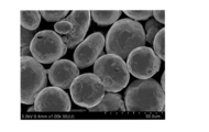
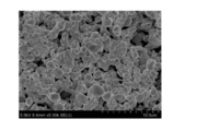
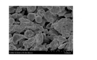
- 4 is an image obtained by photographing the surface of a silver powder (2-1) in an example using a scanning electron microscope (magnification: 1000 times).
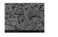
- 5 is an image obtained by photographing the surface of a silver powder (2-2) in an example with a scanning electron microscope (magnification: 1000 times).
- 5 is an image obtained by photographing the surface of a silver powder (2-3) in an example with a scanning electron microscope (magnification: 1000 times).
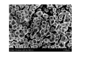
- 4 is an image obtained by photographing the surface of a silver powder (2-4) in an example with a scanning electron microscope (magnification: 20000 times).
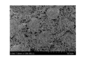
- 9 is an image obtained by photographing the surface of a wiring made of the sintered body of Example 3 with a scanning electron microscope (magnification: 1000 times).
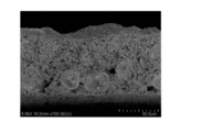
- 9 is an image obtained by photographing a cross section of a wiring made of the sintered body of Example 3 with a scanning electron microscope (magnification: 700 times).
- 9 is an image obtained by photographing the surface of a wiring formed of the sintered body of Example 3 with a scanning electron microscope (magnification: 5000 times).
- 9 is an image obtained by photographing the surface of a wiring made of the sintered body of Example 3 with a scanning electron microscope (magnification: 10000 times).
- 9 is an image obtained by photographing the surface of a wiring formed of the sintered body of Comparative Example 3 with a scanning electron microscope (magnification: 1000 times).
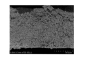
- 9 is an image obtained by photographing a cross section of a wiring made of the sintered body of Comparative Example 3 with a scanning electron microscope (magnification: 700 times).
- 11 is an image obtained by photographing the surface of a wiring formed of the sintered body of Comparative Example 3 with a scanning electron microscope (magnification: 5000 times).
- 11 is an image obtained by photographing the surface of a wiring formed of the sintered body of Comparative Example 3 with a scanning electron microscope (magnification: 10000 times).
- 13 is an image obtained by photographing the surface of a wiring formed of the sintered body of Comparative Example 7 with a scanning electron microscope (400 times magnification).
- 11 is an image obtained by photographing the surface of a wiring formed of the sintered body of Comparative Example 7 with a scanning electron microscope (magnification: 1000 times).
- 6 is an image obtained by photographing a cross section of a sample for measuring shear strength after sintering in Example 3 by using a scanning electron microscope (magnification: 1000 times).
- 5 is an image obtained by photographing a cross section of a sample for measuring shear strength after sintering in Example 3 by using a scanning electron microscope (magnification: 2500 times).
- 9 is an image obtained by photographing a cross section of a sample for measuring shear strength after sintering in Comparative Example 3 with a scanning electron microscope (magnification: 1000 times).
- 9 is an image obtained by photographing a cross section of a sample for measuring shear strength after sintering of Comparative Example 3 by using a scanning electron microscope (magnification: 2500 times).
- the conductive paste of the present invention comprises a flake silver powder having a median diameter D50 of 15 ⁇ m or less, a silver powder having a median diameter D50 of 25 ⁇ m or more, and a solvent, and the flake silver powder and a silver powder having a median diameter D50 of 25 ⁇ m or more.
- the content of the flake silver powder is 15 to 70 parts by mass, and the content of the silver powder having a median diameter D50 of 25 ⁇ m or more is 30 to 85 parts by mass with respect to the total of 100 parts by mass.
- the median diameter D50 of the flake silver powder is 15 ⁇ m or less, preferably 0.1 ⁇ m to 15 ⁇ m, more preferably 2 ⁇ m to 10 ⁇ m.
- the surface area increases as compared with the case where the spherical powder is used, so that a sintered body is easily formed.
- the median diameter D50 of each silver powder means a value measured by a laser diffraction method using SALD-2300 (manufactured by Shimadzu Corporation).
- the flake-like silver powder may be any as long as a majority of particles constituting the silver powder can be recognized as a flake (flake or flake) under a microscope. Typically, it means that 51% by mass or more of the particles (primary particles) constituting the silver powder have a flake (flake or flake) shape.
- the flake-like (flake-like or flake-like) particles mean particles having an aspect ratio (ratio of longest major axis / shortest minor axis) of 5 to 300.
- the silver powder having a median diameter D50 of 25 ⁇ m or more has a median diameter D50 of 25 ⁇ m or more, preferably 25 ⁇ m to 100 ⁇ m, and more preferably 30 ⁇ m to 80 ⁇ m.
- the current flows along each particle, so that the number of contact points of the particles increases and the overall resistivity increases.
- the median diameter of the silver powder having a median diameter D50 of 25 ⁇ m or more is within the above numerical range, one particle contains large particles, so that the number of contact points of the particles can be reduced, and the overall resistivity decreases. . Therefore, a conductive paste having a lower electric resistance value and a higher conductivity when a sintered body is obtained than when only a particle size of less than 25 ⁇ m is used is obtained.
- the shape of the silver powder having a median diameter D50 of 25 ⁇ m or more is not particularly limited, but may be spherical or non-spherical.
- non-spherical, flake-like, needle-like, horn-like, dendritic, granular, irregular, teardrop-like, plate-like, ultra-thin plate-like, hexagonal plate-like, columnar, rod-like, porous, fibrous, Lumped, spongy, horned, rounded and the like are preferable.
- the content of the flaky silver powder is 15 to 70 parts by mass, preferably 30 to 60 parts by mass, and more preferably 30 to 50 parts by mass based on 100 parts by mass of the total of the flaky silver powder and the silver powder having a median diameter D50 of 25 ⁇ m or more. More preferred.
- the content of the silver powder having a median diameter D50 of 25 ⁇ m or more based on 100 parts by mass of the total of the flaky silver powder and the silver powder having a median diameter D50 of 25 ⁇ m or more is 30 to 85 parts by mass, preferably 40 to 70 parts by mass. 50 to 70 parts by mass is more preferred.
- the sintered body has a low electric resistance value, excellent electrical conductivity, and high electron conductivity.
- a conductive paste having excellent bonding strength when bonding substrates and the like is obtained.
- the content of the flaky silver powder with respect to 100 parts by mass of the conductive paste is preferably 10 to 50 parts by mass, more preferably 20 to 50 parts by mass, and most preferably 30 to 50 parts by mass. If the content of the flake silver powder is less than 10 parts by mass with respect to 100 parts by mass of the conductive paste, it is difficult to make the composition containing the flake silver powder into a paste. Further, even if the composition containing the flake silver powder can be made into a paste, the sintered body obtained from such a conductive paste has a high electric resistance value and is inferior in conductivity.
- the content of the silver powder having a median diameter D50 of 25 ⁇ m or more based on 100 parts by mass of the conductive paste is preferably 15 to 60 parts by mass, more preferably 20 to 55 parts by mass, and most preferably 30 to 55 parts by mass.
- the content of the silver powder having a median diameter D50 of 25 ⁇ m or more is within the above-mentioned numerical range, the electrical resistance of the sintered body is low, the electrical conductivity is low, and the bonding strength when an electronic substrate or the like is bonded is improved. An excellent conductive paste is obtained.
- Examples of the solvent include water, alcohol solvents, glycol ether solvents, terpineols, and the like.
- Examples of alcohol solvents include isopropyl alcohol, 1,2-butanediol, isobornylcyclohexanol, 2,4-diethyl-1,5-pentanediol, 2,2-dimethyl-1,3-propanediol, 2,5 -Dimethyl-2,5-hexanediol, 2,5-dimethyl-3-hexyne-2,5-diol, 2,3-dimethyl-2,3-butanediol, 1,1,1-tris (hydroxymethyl) Ethane, 2-ethyl-2-hydroxymethyl-1,3-propanediol, 2,2'-oxybis (methylene) bis (2-ethyl-1,3-propanediol), 2,2-bis (hydroxymethyl) 1,3-propanediol, 1,2,6-trihydroxyhe
- glycol ether solvent examples include diethylene glycol mono-2-ethylhexyl ether, ethylene glycol monophenyl ether, 2-methylpentane-2,4-diol, diethylene glycol monohexyl ether, diethylene glycol dibutyl ether, and triethylene glycol monobutyl ether.
- the content of the solvent with respect to 100 parts by mass of the conductive paste is preferably 2 to 20 parts by mass, more preferably 2 to 15 parts by mass, and most preferably 5 to 10 parts by mass.
- the content of the solvent is within the above numerical range, a paste having good coatability can be obtained.
- the conductive paste of the present invention has a flaky silver powder having a median diameter D50 of 15 ⁇ m or less, a silver powder having a median diameter D50 of 25 ⁇ m or more, and a bimodal powder having peaks at 0.1 ⁇ m to 0.5 ⁇ m and 1 ⁇ m to 15 ⁇ m.
- Silver powder having a particle size distribution, and a solvent the flake silver powder, silver powder having a median diameter D50 of 25 ⁇ m or more, and a total of 100 parts by mass of the silver powder having a bimodal particle size distribution, the flake-like
- the content of silver powder is 8 to 55 parts by mass
- the content of silver powder having a median diameter D50 of 25 ⁇ m or more is 15 to 65 parts by mass
- the content of silver powder having a bimodal particle size distribution is 4 parts by mass. 4545 parts by mass.
- Median diameter D50 of flake silver powder, definition of flake shape, content of flake silver powder with respect to 100 parts by mass of conductive paste, median diameter D50 and shape of silver powder having median diameter D50 of 25 ⁇ m or more, with respect to 100 parts by mass of conductive paste As the content of silver powder having a median diameter D50 of 25 ⁇ m or more, the type of solvent, and the content of solvent with respect to 100 parts by mass of the conductive paste, those described in the first embodiment can be used.
- a silver powder having a bimodal particle size distribution has peaks at 0.1 ⁇ m to 0.5 ⁇ m and 1 ⁇ m to 15 ⁇ m, and preferably has peaks at 0.1 ⁇ m to 0.3 ⁇ m and 3 ⁇ m to 10 ⁇ m.
- the bimodal particle size distribution means a value measured by a laser diffraction method using SALD-2300 (manufactured by Shimadzu Corporation).
- the shape of the silver powder having a bimodal particle size distribution is not particularly limited, but may be spherical or non-spherical.
- non-spherical, flake-like, needle-like, horn-like, dendritic, granular, irregular, teardrop-like, plate-like, ultra-thin plate-like, hexagonal plate-like, columnar, rod-like, porous, fibrous, Lumped, spongy, horned, rounded and the like are examples of such shapes.
- the shape of the silver powder having a bimodal particle size distribution is spherical
- the shape is not limited to a true spherical shape, and any shape may be used as long as the majority of the particles constituting the silver powder are recognized as spherical under a microscope.
- it means that 80% by mass or more of the particles (primary particles) constituting the silver powder have a spherical shape or a shape similar thereto.
- the spherical particles mean particles having an aspect ratio (ratio of major axis / minor axis) of 1.0 to 1.3.
- the content of the flake silver powder is 8 to 55 parts by mass, and 15 to 40 parts by mass with respect to 100 parts by mass of the total of the flake silver powder, the silver powder having a median diameter D50 of 25 ⁇ m or more, and the silver powder having a bimodal particle size distribution. Parts by mass, more preferably 20 to 35 parts by mass.
- the content of the silver powder having a median diameter D50 of 25 ⁇ m or more based on a total of 100 parts by mass of the flake silver powder, the silver powder having a median diameter D50 of 25 ⁇ m or more, and the silver powder having a bimodal particle size distribution is 15 to 65 parts by mass.
- the amount is preferably 20 to 65 parts by mass, more preferably 30 to 60 parts by mass.
- the content of the silver powder having a bimodal particle size distribution with respect to a total of 100 parts by mass of the flaky silver powder, the silver powder having a median diameter D50 of 25 ⁇ m or more, and the silver powder having a bimodal particle size distribution is 4 to 45 parts by mass. And preferably 10 to 40 parts by mass, more preferably 15 to 30 parts by mass.
- the sintered body When the content of the flake silver powder, the content of the silver powder having a median diameter D50 of 25 ⁇ m or more, and the content of the silver powder having a bimodal particle size distribution were all within the above numerical ranges, the sintered body was obtained. In this case, a conductive paste having a low electric resistance value, excellent conductivity, and excellent joining strength when an electronic substrate or the like is joined can be obtained.
- the content of silver powder having a bimodal particle size distribution with respect to 100 parts by mass of the conductive paste is preferably 5 to 40 parts by mass, more preferably 10 to 35 parts by mass, and most preferably 10 to 30 parts by mass.
- the conductive paste of the present invention is prepared by using ARV-310 (manufactured by Sinky Co., Ltd.) using flake silver powder, silver powder having a median diameter D50 of 25 ⁇ m or more, a solvent, and optionally silver powder having a bimodal particle size distribution. ) It can be kneaded and manufactured using an apparatus.
- the present invention provides a sintered body obtained by sintering the above conductive paste.
- a sintered body can be obtained by printing or applying a conductive paste on a substrate and then sintering. Since such a sintered body has conductivity, it functions as a wiring (electronic circuit) on a substrate.
- the method of printing or applying the conductive paste is not particularly limited, and examples thereof include dispense application, print application, spray application, brushing, and injection.
- the substrate on which the sintered body is provided is not particularly limited, but a glass fiber reinforced epoxy printed board such as FR4 having high heat resistance, a polyimide-based board, a ceramic such as DBA (Direct Bonded Aluminum) or DBC (Direct Bonded Copper).
- a glass fiber reinforced epoxy printed board such as FR4 having high heat resistance
- a polyimide-based board such as DBA (Direct Bonded Aluminum) or DBC (Direct Bonded Copper).
- DBA Direct Bonded Aluminum
- DBC Direct Bonded Copper
- Substrates, metal substrates such as copper, silver, and aluminum, and Cu lead frames are exemplified. Electronic components are mounted on the substrate.
- the metal substrate may be plated with metal. Examples of the metal used for metal plating include gold, silver, nickel, and tin.
- the conditions for sintering the conductive paste are not particularly limited, but the heating temperature in sintering is preferably 150 to 350 ° C, more preferably 180 to 300 ° C, and most preferably 200 to 300 ° C.
- the heating time in sintering is preferably from 10 to 60 minutes, more preferably from 15 to 45 minutes, and most preferably from 20 to 30 minutes. No pressure is applied to the conductive paste during sintering.
- the sintering can be performed in an air atmosphere or an atmosphere having an oxygen concentration of 1% or more.
- the shape of the sintered body is not particularly limited, and examples thereof include a sheet, a film, a tape, a line, a disk, a block, a spot, and an irregular shape.
- the sintered body of the present invention can achieve an electric resistance value of 8.5 ⁇ ⁇ cm or less.
- the electric resistance value of the sintered body can be measured by the method described in “(1) Evaluation of electric resistance value” of (Evaluation) described later.
- the present invention provides a sintered body obtained by sintering a laminate including a substrate, the above-mentioned conductive paste, and a conductor.
- a laminate can be manufactured by sequentially laminating a conductive paste and a conductor on a substrate. Then, a sintered body can be obtained by sintering the laminate. In such a sintered body, a portion derived from the conductive paste has conductivity and bonds the substrate and the conductor, and thus functions as a conductive bonding portion (adhesion portion).
- the substrate to be bonded include a circuit substrate, a glass fiber reinforced epoxy-based printed substrate, a polyimide-based substrate, a ceramic substrate, a metal substrate, a Cu lead frame, and the like.
- Examples of the conductor to be bonded include chip components such as a capacitor and a resistor, a chip obtained by forming a semiconductor element such as a resistor, a transistor, a capacitor, and an integrated circuit on a wafer and then cutting a section of each semiconductor element from the wafer. Is mentioned.
- Conditions for sintering the above-mentioned laminated body differ depending on an object to be joined.
- the conditions are as follows. The conditions under an air atmosphere are mentioned.
- the above laminated body after sintering can achieve a shear strength of 25 MPa or more.
- the shear strength means a value measured by a method in accordance with JIS Z 3198, and the bonding strength (shear strength) of the laminated body after sintering is described in “(2) of (Evaluation) described later. Evaluation of Shear Strength ".
- Example 1 (1) Evaluation of Electric Resistance
- the conductive pastes of Examples 1 to 11 and Comparative Examples 1 to 13 were applied to a glass substrate (2 mm in thickness) by screen printing using a metal mask (100 ⁇ m in thickness).
- the glass substrate to which the conductive paste was applied was heated at 200 ° C. for 30 minutes under atmospheric pressure and atmospheric pressure, and sintering was performed to form wiring.
- the wiring by the sintered body of the conductive paste thus obtained was 3 mm ⁇ 30 mm in length ⁇ width.
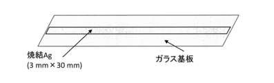
- FIG. 1 shows a schematic diagram of the obtained wiring.
- a copper substrate (length ⁇ width: 50 mm ⁇ 50 mm) in which a Ti layer (thickness: 40 nm) and an Ag layer (thickness: 1000 nm) are laminated in order from the copper substrate side (hereinafter, a test piece) (Referred to as (1)).
- the conductive pastes of Examples 1 to 11 and Comparative Examples 1 to 13 were screen-printed on the Ag layer of the test piece (1) using a metal mask (thickness: 100 ⁇ m).
- a Si chip (length ⁇ width: 3 mm ⁇ 3 mm) in which a Ti layer (thickness: 40 nm) and an Ag layer (thickness: 1000 nm) are laminated by sputtering in order from the Si chip side (hereinafter, referred to as a test piece (2)) was prepared.
- Example 1 to 3 and 5 to 11 and Comparative Examples 1 to 3 and 5 to 13 a chip mounter (product name SMT-64RH, product name) was placed on the conductive paste applied to the test piece (1).
- the Ag layer side of the test piece (2) was laminated using Okuhara Electric Co., Ltd. to obtain a sample including the test piece (1), the conductive paste, and the test piece (2).
- the obtained sample was heated at 200 ° C. for 30 minutes under atmospheric pressure and atmospheric pressure to perform sintering.
- Example 4 and Comparative Example 4 using ethanol as a solvent when a chip mounter was used, the solvent was volatilized before the test piece (2) was laminated on the conductive paste, and the test piece (2) was used.
- Example 4 shows a schematic diagram of the obtained sample after sintering.
- Example 1 to 11 Comparative Examples 1 to 13
- a commercially available product name AgC239 manufactured by Fukuda Metal Foil & Powder Co., Ltd., median diameter D50: 2.5 ⁇ m, flake shape
- silica powder (1) a commercially available product name AgC239 (manufactured by Fukuda Metal Foil & Powder Co., Ltd., median diameter D50: 2.5 ⁇ m, flake shape)
- silver powder (2-1) two types of silver powder having a median diameter D50 of 25 ⁇ m or more
- siver powder (2-2) two types of silver powder having a median diameter D50 of 25 ⁇ m or more
- silver powder (2-2) a silver powder having a median diameter D50 of less than 25 ⁇ m
- silver powder (2-4) silver powder having a particle size distribution of 300 to 700 nm
- silver powder (3) silver powder having a bimodal particle size distribution
- Spherical silver powder having a median diameter D50: 36.34 ⁇ m was obtained by heating silver to a molten state, spraying the molten silver, and cooling (melt spraying method). 2-1) was prepared.
- Silver powder having a peak at 300 to 700 nm was produced by the following production method. First, 1.0 g of silver nitrate (silver compound) was dissolved in 50 g of ethylene glycol (polyhydric alcohol). Next, 0.5 g of polyvinylpyrrolidone (dispersant) was dispersed in ethylene glycol. Next, after the ethylene glycol was heated to 150 ° C. (reaction temperature), the reaction was carried out for 1 hour while stirring at a rotation speed of 500 rpm while maintaining the reaction temperature at 150 ° C. The silver powder after the reaction was separated from ethylene glycol (polyhydric alcohol) using a metal mesh, and the separated silver powder was washed with ethanol to obtain silver powder (2-4).
- 3A to 3D show images of the obtained silver powders (2-1) to (2-4) taken by a field emission scanning electron microscope (FE-SEM) (JSM-7000F manufactured by JEOL Ltd.).
- 3A to 3C are photographs of the surfaces of the silver powders (2-1) to (2-3) at a magnification of 1000 times
- FIG. 3D is a photograph of the surfaces of the silver powders (2-4) at a magnification of 20000 times. It was done.
- silver powder (2) the silver powders (2-1) to (2-4) are collectively referred to as silver powder (2).
- Silver powder (3) having a bimodal particle size distribution having peaks at 0.1 ⁇ m to 0.5 ⁇ m and 1 ⁇ m to 15 ⁇ m was produced by the following production method.
- silver powder A was produced by exactly the same production method as silver powder (2-4). Then, while stirring 50 g of ethylene glycol at a rotation speed of 500 rpm, 2.0 g of silver nitrate was dissolved in ethylene glycol, and then 0.05 g of silver powder A was further dispersed in ethylene glycol. Next, after the ethylene glycol was heated to 150 ° C. (reaction temperature), the reaction was carried out for 1 hour while stirring at a rotation speed of 500 rpm while maintaining the reaction temperature at 150 ° C. Thereafter, the silver powder after the reaction was separated from ethylene glycol using a metal mesh, and the separated silver powder was washed with ethanol to obtain silver powder (3).
- the median diameter D50 of the silver powders (1) and (2-1) to (2-3) and the particle size distribution of the silver powder (2-4) and the silver powder (3) used in this example and the comparative example are SALD- 2300 (manufactured by Shimadzu Corporation) was measured by a laser diffraction method.
- the conductive pastes of Examples 1 to 11 each contained flake silver powder having a median diameter D50 of 15 ⁇ m or less, silver powder having a median diameter D50 of 25 ⁇ m or more, and a solvent, and contained the flake silver powder and the median diameter D50 of 25 ⁇ m or more.
- the content of the flaky silver powder is 15 to 70 parts by mass, and the content of the silver powder having a median diameter D50 of 25 ⁇ m or more is 30 to 85 parts by mass with respect to a total of 100 parts by mass of the silver powder having It is a conductive paste.
- the electric resistance value of the wiring made of the sintered body is low, and has better conductivity, and the sintered body has excellent shear strength and has better jointability.
- the content of the flake silver powder was 30 to 42 parts by mass with respect to the total of 100 parts by mass of the flake silver powder and the silver powder having a median diameter D50 of 25 ⁇ m or more, and the median diameter of 25 ⁇ m or more was used.
- Comparative Example 1 shown in Table 2 above is a conductive paste containing no silver powder (1) and silver powder (2).
- Comparative Examples 2 to 4 and 10 are conductive pastes containing no silver powder (2).
- Comparative Examples 7 and 9 are conductive pastes containing no silver powder (1).
- Comparative Examples 5 and 8 contain both the silver powder (1) and the silver powder (2-1), but the silver powder (1) was added to the silver powder (1) and the silver powder (2-1) in a total of 100 parts by mass.
- the conductive paste has a content of less than 15 parts by mass and a silver powder (2-1) content of more than 85 parts by mass.
- Comparative Example 6 contained both silver powder (1) and silver powder (2-1), but the content of silver powder (1) was 100 parts by mass in total of silver powder (1) and silver powder (2). Is more than 70 parts by mass and the content of silver powder (2-1) is less than 30 parts by mass.
- Comparative Examples 11 to 13 are conductive pastes containing no silver powder and having a median diameter D50 of 25 ⁇ m or more.
- the conductive pastes of Comparative Examples 1 to 5, 7 to 10, and 13 have a lower electric resistance value of the wiring made of the sintered body than the conductive pastes of Examples 1 to 13. It was high, the conductivity was insufficient, and the shear strength of the sintered body was low, and the bondability was poor.
- the conductive paste of Comparative Example 6 although the sintered body had good bonding properties, the electrical resistance of the wiring formed by the sintered body was high and the conductivity was insufficient.
- the wiring of the sintered body had good conductivity, but the shear strength of the sintered body was low and the bonding property was poor.
- 4A to 6B show images of the wirings of the sintered bodies of Example 3 and Comparative Examples 3 and 7 taken by a field emission scanning electron microscope (FE-SEM) (JSM-7000F manufactured by JEOL).
- 4A, 4C, and 4D are photographs of the surface of the wiring of Example 3 at magnifications of 1,000, 5,000, and 10,000, respectively.
- FIG. 4B is a photograph of a cross section of the wiring of Example 3 taken at a magnification of 700 times.
- 5A, 5C, and 5D are photographs of the surface of the wiring of Comparative Example 3 at magnifications of 1,000, 5,000, and 10,000, respectively.
- FIG. 5B is a photograph of a cross section of the wiring of Comparative Example 3 taken at a magnification of 700 times.
- 6A and 6B are photographs of the surface of the wiring of Comparative Example 7 at magnifications of 400 and 1000, respectively.
- Example 3 in the wiring of Example 3, the silver powder (1) having a small diameter and a flaky silver powder (2-1), the silver powder having a large diameter (2-1), and the silver powder (3) having a small diameter and a bimodal particle size distribution were obtained. ) Were observed in the sintered body. Then, in the wiring of Example 3, it was found that the flake silver particles and the silver particles having a small diameter and the silver particles having a large diameter were sufficiently in contact with each other and fused. As a result, it is considered that in the wiring of Example 3, the moving speed of the electrons in the wiring was increased, and the electric resistance was reduced.
- the wiring of Comparative Example 3 in the wiring of Comparative Example 3, the structures derived from the flake silver powder (1) having a small diameter and the silver powder (3) having a small diameter and a bimodal particle size distribution were respectively sintered. Observed in the body.
- the wiring of Comparative Example 3 is composed of only the silver powders (1) and (3) having a small diameter and does not include the silver powder (2-1) or (2-2) having a large diameter. It was found that the silver particles were not sufficiently in contact with each other and were not sufficiently fused in other portions, although they were in some contact. Thus, it is considered that the electrical resistance of the wiring of Comparative Example 3 was higher than that of the wiring of Example 3.
- the wiring of Comparative Example 7 is composed of only the large-diameter silver powder (2-1) and does not include the small-diameter silver powders (1) and (3). It was found that silver particles existed independently and hardly fused together. Thus, it is considered that the electrical resistance value of the wiring of Comparative Example 7 was extremely high.
- 7A to 8B show images of the samples for measuring the shear strength after sintering of Example 3 and Comparative Example 3 taken by a field emission scanning electron microscope (FE-SEM) (JSM-7000F manufactured by JEOL). Show. 7A and 7B are cross-sectional images of the sample of Example 3 taken at magnifications of 1000 and 2500, respectively. 8A and 8B are cross-sectional images of the sample of Comparative Example 3 taken at magnifications of 1000 and 2500, respectively.
- FE-SEM field emission scanning electron microscope
- the sample of Comparative Example 3 is composed of only the small-diameter silver powders (1) and (3) and does not include the large-diameter silver powder (2-1) or (2-2). Therefore, it was found that the contact area between the silver particles was small and did not sufficiently fuse, so that there were many voids inside the sintered body. Thus, it is considered that the shear strength of the sample of Comparative Example 3 was lower than that of the sample of Example 3.
- the flake silver powder having a median diameter D50 of 15 ⁇ m or less, the silver powder having a median diameter D50 of 25 ⁇ m or more, and a solvent, the flake silver powder and the median diameter D50 of 25 ⁇ m or more are included.
Landscapes
- Chemical & Material Sciences (AREA)
- Dispersion Chemistry (AREA)
- Engineering & Computer Science (AREA)
- Microelectronics & Electronic Packaging (AREA)
- Spectroscopy & Molecular Physics (AREA)
- Physics & Mathematics (AREA)
- Materials Engineering (AREA)
- Mechanical Engineering (AREA)
- Metallurgy (AREA)
- Organic Chemistry (AREA)
- Conductive Materials (AREA)
- Powder Metallurgy (AREA)
- Parts Printed On Printed Circuit Boards (AREA)
- Die Bonding (AREA)
- Non-Insulated Conductors (AREA)
Abstract
本発明は、焼結体とした際の電気抵抗値が低く導電性に優れた導電性ペースト及びその焼結体を提供することを目的とする。 15μm以下のメディアン径D50を有するフレーク状銀粉、25μm以上のメディアン径D50を有する銀粉、及び溶剤を含み、 前記フレーク状銀粉と前記25μm以上のメディアン径D50を有する銀粉との合計100質量部に対して、前記フレーク状銀粉の含有量が15~70質量部であり、前記25μm以上のメディアン径D50を有する銀粉の含有量が30~85質量部であることを特徴とする導電性ペースト。
Description
本発明は、導電性ペースト及び焼結体に関する。
従来、μmサイズ(以下、「ミクロンサイズ」ということがある。)又はnmサイズ(以下、「ナノサイズ」ということがある。)の金属粉を用いた導電性ペーストは、導電性材料として広く用いられている。このようなミクロンサイズ又はナノサイズの金属粉を用いた導電性ペーストは、例えば、プリント配線基板における電極、配線などの電子回路の形成や、電子基板と電子部品との間の接合に使用されている。
このような金属粉を用いた導電性ペーストとして、特許文献1においては、平均粒径が0.1~18μmであり、炭素量が1.0重量%以下である非球状銀粒子と、揮発性分散媒とからなるペースト状物であり、加熱により該揮発性分散媒が揮散し該非球状銀粒子同士が焼結することを特徴とするペースト状銀粒子組成物が提案されている。特許文献1においては、上記非球状銀粒子として、フレーク状銀粒子を用いた導電性ペーストが具体的に開示されている。しかし、本願の比較例2において後述するように、特許文献1に記載されているような、18μm以下の小さな平均粒径の銀粒子(銀粉)のみを用いた導電性ペーストは、焼結させて配線とした際の電気抵抗値が高く、導電性が十分ではない。
また、特許文献2においては、0.1μm~15μmの平均粒径(メジアン径)を有する銀粒子と、アルコールとを含む導電性ペーストが提案されている。特許文献2においては、上記銀粒子として、平均粒径(メジアン径)が0.3μmの銀粒子と平均粒径(メジアン径)が2.0~3.2μmの銀粒子との2種類を混合した導電性ペーストが具体的に開示されている。しかし、本願の比較例3及び4において後述するように、特許文献2に記載されているような、15μm以下の小さな平均粒径の2種類の銀粒子(銀粉)のみを混合した導電性ペーストは、焼結させて配線とした際の電気抵抗値が高く、導電性が十分ではない。
特許文献3においては、銀粉末を主体とする導体ペーストの製造方法であって、相互に平均粒径が異なる少なくとも2種の球状銀粉末と、相互に平均粒径が異なる少なくとも2種のフレーク状銀粉末とが混合されて成る導電性粉末を用意する工程と、前記導電性粉末を有機媒質中に分散させる工程と、を包含する製造方法が提案されている。特許文献3においては、上記少なくとも2種の球状銀粉末及び少なくとも2種のフレーク状銀粉末として、平均粒径0.1~0.8μmの球状銀粉末、平均粒径1.0~2.0μmの球状銀粉末、平均粒径1~4μmのフレーク状銀粉末、及び平均粒径5~15μmのフレーク状銀粉末の組み合わせを用いることも開示されている。しかし、特許文献3に記載されている4種類の銀粉末は、いずれも15μm以下の小さな平均粒径を有するものである。本願の比較例11~13において後述するように、特許文献3に記載されているような、25μm以上のメディアン径を有する銀粉を含まない導電性ペーストは、電子基板と電子部品とを接合した際の接合強度が十分ではない。
特許文献4においては、銀箔を粉砕して得られた平均粒径45μm~1000μmでしわくちゃ状銀粉を含む見掛密度0.01g/cm3~0.1g/cm3の嵩高銀粉の充填量が5重量%以上25重量%未満、接着剤の充填量が75重量%を越えて95重量%以下であることを特徴とする導電性接着剤が提案されている。しかし、特許文献4に記載の導電性接着剤は、高分子化合物を含有することを前提としており、銀粉のみを溶剤と混合した導電性ペーストとは異なる材料である。
従来の導電性ペーストは、プリント配線基板上に塗布後に焼結させて配線とした際の電気抵抗値が高く、導電性が十分ではなく、また、電子基板と電子部品とを接合した際の接合強度も十分ではないという問題がある。
したがって、焼結体とした際の電気抵抗値が低く導電性に優れた導電性ペーストが望まれている。さらに、優れた導電性に加えて電子基板等を接合した際の接合強度に優れた導電性ペーストも望まれている。
本発明は、焼結体とした際の電気抵抗値が低く導電性に優れた導電性ペースト及びその焼結体を提供することを目的とする。また、本発明は、優れた導電性に加えて電子基板等を接合した際の接合強度にも優れた導電性ペースト及びその焼結体を提供することも別の目的とする。
本発明者らは、上記課題を解決するべく鋭意研究した結果、特定量の15μm以下のメディアン径D50を有するフレーク状銀粉、特定量の25μm以上のメディアン径D50を有する銀粉、及び溶剤を組み合わせて用いることで上記課題を解決できることを知見し、本発明を完成するに至った。本発明の具体的態様は以下のとおりである。
なお、本明細書において、「~」を用いて数値範囲を表す際は、その範囲は両端の数値を含むものとする。
なお、本明細書において、「~」を用いて数値範囲を表す際は、その範囲は両端の数値を含むものとする。
[1] 15μm以下のメディアン径D50を有するフレーク状銀粉、25μm以上のメディアン径D50を有する銀粉、及び溶剤を含み、
前記フレーク状銀粉と前記25μm以上のメディアン径D50を有する銀粉との合計100質量部に対して、前記フレーク状銀粉の含有量が15~70質量部であり、前記25μm以上のメディアン径D50を有する銀粉の含有量が30~85質量部であることを特徴とする導電性ペースト。
[2] 15μm以下のメディアン径D50を有するフレーク状銀粉、25μm以上のメディアン径D50を有する銀粉、0.1μm~0.5μmと1μm~15μmとにピークを有する二峰性の粒度分布を有する銀粉、及び溶剤を含み、
前記フレーク状銀粉、前記25μm以上のメディアン径D50を有する銀粉、及び前記二峰性の粒度分布を有する銀粉の合計100質量部に対して、前記フレーク状銀粉の含有量が8~55質量部であり、前記25μm以上のメディアン径D50を有する銀粉の含有量が15~65質量部であり、前記二峰性の粒度分布を有する銀粉の含有量が4~45質量部であることを特徴とする導電性ペースト。
[3] 前記フレーク状銀粉と前記25μm以上のメディアン径D50を有する銀粉との合計100質量部に対して、前記フレーク状銀粉の含有量が30~42質量部であり、前記25μm以上のメディアン径D50を有する銀粉の含有量が58~70質量部であることを特徴とする[1]に記載の導電性ペースト。
[4] 前記フレーク状銀粉、前記25μm以上のメディアン径D50を有する銀粉、及び前記二峰性の粒度分布を有する銀粉の合計100質量部に対して、前記フレーク状銀粉の含有量が23~35質量部であり、前記25μm以上のメディアン径D50を有する銀粉の含有量が40~63質量部であり、前記二峰性の粒度分布を有する銀粉の含有量が12~35質量部であることを特徴とする[2]に記載の導電性ペースト。
[5] [1]~[4]のいずれか1つに記載の導電性ペーストを焼結してなる焼結体。
[6] 基板、[1]~[4]のいずれか1つに記載の導電性ペースト、及び導電体を含む積層体を焼結してなる焼結体。
前記フレーク状銀粉と前記25μm以上のメディアン径D50を有する銀粉との合計100質量部に対して、前記フレーク状銀粉の含有量が15~70質量部であり、前記25μm以上のメディアン径D50を有する銀粉の含有量が30~85質量部であることを特徴とする導電性ペースト。
[2] 15μm以下のメディアン径D50を有するフレーク状銀粉、25μm以上のメディアン径D50を有する銀粉、0.1μm~0.5μmと1μm~15μmとにピークを有する二峰性の粒度分布を有する銀粉、及び溶剤を含み、
前記フレーク状銀粉、前記25μm以上のメディアン径D50を有する銀粉、及び前記二峰性の粒度分布を有する銀粉の合計100質量部に対して、前記フレーク状銀粉の含有量が8~55質量部であり、前記25μm以上のメディアン径D50を有する銀粉の含有量が15~65質量部であり、前記二峰性の粒度分布を有する銀粉の含有量が4~45質量部であることを特徴とする導電性ペースト。
[3] 前記フレーク状銀粉と前記25μm以上のメディアン径D50を有する銀粉との合計100質量部に対して、前記フレーク状銀粉の含有量が30~42質量部であり、前記25μm以上のメディアン径D50を有する銀粉の含有量が58~70質量部であることを特徴とする[1]に記載の導電性ペースト。
[4] 前記フレーク状銀粉、前記25μm以上のメディアン径D50を有する銀粉、及び前記二峰性の粒度分布を有する銀粉の合計100質量部に対して、前記フレーク状銀粉の含有量が23~35質量部であり、前記25μm以上のメディアン径D50を有する銀粉の含有量が40~63質量部であり、前記二峰性の粒度分布を有する銀粉の含有量が12~35質量部であることを特徴とする[2]に記載の導電性ペースト。
[5] [1]~[4]のいずれか1つに記載の導電性ペーストを焼結してなる焼結体。
[6] 基板、[1]~[4]のいずれか1つに記載の導電性ペースト、及び導電体を含む積層体を焼結してなる焼結体。
本発明の導電性ペースト及びその焼結体は、焼結体とした際の電気抵抗値が低く導電性に優れる。
また、本発明の導電性ペースト及び焼結体は、優れた導電性に加えて電子基板等を接合した際の接合強度にも優れる。
また、本発明の導電性ペースト及び焼結体は、優れた導電性に加えて電子基板等を接合した際の接合強度にも優れる。
以下、本発明の導電性ペースト及び焼結体について、説明する。
[第一の実施形態]
本発明の導電性ペーストは、15μm以下のメディアン径D50を有するフレーク状銀粉、25μm以上のメディアン径D50を有する銀粉、及び溶剤を含み、前記フレーク状銀粉と前記25μm以上のメディアン径D50を有する銀粉との合計100質量部に対して、前記フレーク状銀粉の含有量が15~70質量部であり、前記25μm以上のメディアン径D50を有する銀粉の含有量が30~85質量部である。
本発明の導電性ペーストは、15μm以下のメディアン径D50を有するフレーク状銀粉、25μm以上のメディアン径D50を有する銀粉、及び溶剤を含み、前記フレーク状銀粉と前記25μm以上のメディアン径D50を有する銀粉との合計100質量部に対して、前記フレーク状銀粉の含有量が15~70質量部であり、前記25μm以上のメディアン径D50を有する銀粉の含有量が30~85質量部である。
フレーク状銀粉のメディアン径D50は、15μm以下であり、0.1μm~15μmが好ましく、2μm~10μmがより好ましい。フレーク状銀粉のメディアン径D50が上記数値範囲内であると、球状粉を使用した場合よりも表面積が増えるので、焼結体が形成されやすくなる。
本発明において、各銀粉のメディアン径D50は、SALD-2300(島津製作所製)を用いて、レーザー回折法により測定したものを意味する。
本発明において、フレーク状銀粉は、当該銀粉を構成する粒子の過半数が顕微鏡下でフレーク状(薄片状又は剥片状)と認められるものであればよい。典型的には、当該銀粉を構成する粒子(一次粒子)の51質量%以上がフレーク(薄片又は剥片)形状を有していることをいう。ここで、フレーク状(薄片状又は剥片状)の粒子とは、アスペクト比(最も長い長径/最も短い短径の比)が5~300である粒子を意味する。
25μm以上のメディアン径D50を有する銀粉のメディアン径D50は、25μm以上であり、25μm~100μmが好ましく、30μm~80μmがより好ましい。
25μm未満の粒径のみを使用した場合は、電流は各粒子を伝って流れるので、粒子の接点数が多くなり、全体の抵抗率が高くなる。一方、25μm以上のメディアン径D50を有する銀粉のメディアン径が上記数値範囲内であると、1粒が大きい粒子を含むので、粒子の接点数を少なくすることができ、全体の抵抗率が低くなる。よって、25μm未満の粒径のみを使用した場合よりも焼結体とした際の電気抵抗値が低く導電性に優れる導電性ペーストが得られる。
25μm未満の粒径のみを使用した場合は、電流は各粒子を伝って流れるので、粒子の接点数が多くなり、全体の抵抗率が高くなる。一方、25μm以上のメディアン径D50を有する銀粉のメディアン径が上記数値範囲内であると、1粒が大きい粒子を含むので、粒子の接点数を少なくすることができ、全体の抵抗率が低くなる。よって、25μm未満の粒径のみを使用した場合よりも焼結体とした際の電気抵抗値が低く導電性に優れる導電性ペーストが得られる。
25μm以上のメディアン径D50を有する銀粉の形状は、特に限定されないが、球状及び非球状のいずれでもよい。非球状の例としては、フレーク状、針状、角状、樹枝状、粒状、不規則形状、涙滴状、板状、極薄板状、六角板状、柱状、棒状、多孔状、繊維状、塊状、海綿状、けい角状、丸み状等が挙げられる。このような形状の中でも、球状、柱状が好ましい。
フレーク状銀粉と25μm以上のメディアン径D50を有する銀粉との合計100質量部に対するフレーク状銀粉の含有量は、15~70質量部であり、30~60質量部が好ましく、30~50質量部がより好ましい。
フレーク状銀粉と25μm以上のメディアン径D50を有する銀粉との合計100質量部に対する25μm以上のメディアン径D50を有する銀粉の含有量は、30~85質量部であり、40~70質量部が好ましく、50~70質量部がより好ましい。
フレーク状銀粉の含有量及び25μm以上のメディアン径D50を有する銀粉の含有量のいずれもが上記数値範囲内であると、焼結体とした際の電気抵抗値が低く導電性に優れる上に電子基板等を接合した際の接合強度に優れる導電性ペーストが得られる。
導電性ペースト100質量部に対するフレーク状銀粉の含有量は、10~50質量部が好ましく、20~50質量部がより好ましく、30~50質量部が最も好ましい。
導電性ペースト100質量部に対するフレーク状銀粉の含有量が10質量部未満であると、フレーク状銀粉を含む組成物をペースト状とすることが困難である。また、仮にフレーク状銀粉を含む組成物をペースト状とすることが可能であったとしても、このような導電性ペーストから得られる焼結体は、電気抵抗値が高くなり導電性に劣る。
導電性ペースト100質量部に対するフレーク状銀粉の含有量が10質量部未満であると、フレーク状銀粉を含む組成物をペースト状とすることが困難である。また、仮にフレーク状銀粉を含む組成物をペースト状とすることが可能であったとしても、このような導電性ペーストから得られる焼結体は、電気抵抗値が高くなり導電性に劣る。
導電性ペースト100質量部に対する25μm以上のメディアン径D50を有する銀粉の含有量は、15~60質量部が好ましく、20~55質量部がより好ましく、30~55質量部が最も好ましい。25μm以上のメディアン径D50を有する銀粉の含有量が上記数値範囲内であると、焼結体とした際の電気抵抗値が低く導電性に優れる上に電子基板等を接合した際の接合強度に優れる導電性ペーストが得られる。
溶剤としては、水、アルコール系溶剤、グリコールエーテル系溶剤、テルピネオール類等が挙げられる。
アルコール系溶剤としてはイソプロピルアルコール、1,2-ブタンジオール、イソボルニルシクロヘキサノール、2,4-ジエチル-1,5-ペンタンジオール、2,2-ジメチル-1,3-プロパンジオール、2,5-ジメチル-2,5-ヘキサンジオール、2,5-ジメチル-3-ヘキシン-2,5-ジオール、2,3-ジメチル-2,3-ブタンジオール、1,1,1-トリス(ヒドロキシメチル)エタン、2-エチル-2-ヒドロキシメチル-1,3-プロパンジオール、2,2′-オキシビス(メチレン)ビス(2-エチル-1,3-プロパンジオール)、2,2-ビス(ヒドロキシメチル)-1,3-プロパンジオール、1,2,6-トリヒドロキシヘキサン、ビス[2,2,2-トリス(ヒドロキシメチル)エチル]エーテル、1-エチニル-1-シクロヘキサノール、1,4-シクロヘキサンジオール、1,4-シクロヘキサンジメタノール、エリトリトール、トレイトール、グアヤコールグリセロールエーテル、3,6-ジメチル-4-オクチン-3,6-ジオール、2,4,7,9-テトラメチル-5-デシン-4,7-ジオール等が挙げられる。
グリコールエーテル系溶剤としては、ジエチレングリコールモノ-2-エチルヘキシルエーテル、エチレングリコールモノフェニルエーテル、2-メチルペンタン-2,4-ジオール、ジエチレングリコールモノヘキシルエーテル、ジエチレングリコールジブチルエーテル、トリエチレングリコールモノブチルエーテル等が挙げられる。
アルコール系溶剤としてはイソプロピルアルコール、1,2-ブタンジオール、イソボルニルシクロヘキサノール、2,4-ジエチル-1,5-ペンタンジオール、2,2-ジメチル-1,3-プロパンジオール、2,5-ジメチル-2,5-ヘキサンジオール、2,5-ジメチル-3-ヘキシン-2,5-ジオール、2,3-ジメチル-2,3-ブタンジオール、1,1,1-トリス(ヒドロキシメチル)エタン、2-エチル-2-ヒドロキシメチル-1,3-プロパンジオール、2,2′-オキシビス(メチレン)ビス(2-エチル-1,3-プロパンジオール)、2,2-ビス(ヒドロキシメチル)-1,3-プロパンジオール、1,2,6-トリヒドロキシヘキサン、ビス[2,2,2-トリス(ヒドロキシメチル)エチル]エーテル、1-エチニル-1-シクロヘキサノール、1,4-シクロヘキサンジオール、1,4-シクロヘキサンジメタノール、エリトリトール、トレイトール、グアヤコールグリセロールエーテル、3,6-ジメチル-4-オクチン-3,6-ジオール、2,4,7,9-テトラメチル-5-デシン-4,7-ジオール等が挙げられる。
グリコールエーテル系溶剤としては、ジエチレングリコールモノ-2-エチルヘキシルエーテル、エチレングリコールモノフェニルエーテル、2-メチルペンタン-2,4-ジオール、ジエチレングリコールモノヘキシルエーテル、ジエチレングリコールジブチルエーテル、トリエチレングリコールモノブチルエーテル等が挙げられる。
導電性ペースト100質量部に対する溶剤の含有量は、2~20質量部が好ましく、2~15質量部がより好ましく、5~10質量部が最も好ましい。溶剤の含有量が上記数値範囲内であることにより、塗布性の良いペーストを得ることができる。
[第二の実施形態]
本発明の導電性ペーストは、15μm以下のメディアン径D50を有するフレーク状銀粉、25μm以上のメディアン径D50を有する銀粉、0.1μm~0.5μmと1μm~15μmとにピークを有する二峰性の粒度分布を有する銀粉、及び溶剤を含み、前記フレーク状銀粉、前記25μm以上のメディアン径D50を有する銀粉、及び前記二峰性の粒度分布を有する銀粉の合計100質量部に対して、前記フレーク状銀粉の含有量が8~55質量部であり、前記25μm以上のメディアン径D50を有する銀粉の含有量が15~65質量部であり、前記二峰性の粒度分布を有する銀粉の含有量が4~45質量部である。
本発明の導電性ペーストは、15μm以下のメディアン径D50を有するフレーク状銀粉、25μm以上のメディアン径D50を有する銀粉、0.1μm~0.5μmと1μm~15μmとにピークを有する二峰性の粒度分布を有する銀粉、及び溶剤を含み、前記フレーク状銀粉、前記25μm以上のメディアン径D50を有する銀粉、及び前記二峰性の粒度分布を有する銀粉の合計100質量部に対して、前記フレーク状銀粉の含有量が8~55質量部であり、前記25μm以上のメディアン径D50を有する銀粉の含有量が15~65質量部であり、前記二峰性の粒度分布を有する銀粉の含有量が4~45質量部である。
フレーク状銀粉のメディアン径D50、フレーク形状の定義、導電性ペースト100質量部に対するフレーク状銀粉の含有量、25μm以上のメディアン径D50を有する銀粉のメディアン径D50及び形状、導電性ペースト100質量部に対する25μm以上のメディアン径D50を有する銀粉の含有量、溶剤の種類、並びに導電性ペースト100質量部に対する溶剤の含有量としては、第一の実施形態において示したものを使用することができる。
二峰性の粒度分布を有する銀粉は、0.1μm~0.5μmと1μm~15μmとにピークを有し、好ましくは0.1μm~0.3μmと3μm~10μmとにピークを有する。
本発明において、二峰性の粒度分布は、SALD-2300(島津製作所製)を用いて、レーザー回折法により測定したものを意味する。
二峰性の粒度分布を有する銀粉の形状は、特に限定されないが、球状及び非球状のいずれでもよい。非球状の例としては、フレーク状、針状、角状、樹枝状、粒状、不規則形状、涙滴状、板状、極薄板状、六角板状、柱状、棒状、多孔状、繊維状、塊状、海綿状、けい角状、丸み状等が挙げられる。このような形状の中でも、球状が好ましい。
二峰性の粒度分布を有する銀粉の形状が球状である場合、真球状のものに限られず、当該銀粉を構成する粒子の過半数が顕微鏡下で球状と認められるものであればよい。典型的には、当該銀粉を構成する粒子(一次粒子)の80質量%以上が球状又はそれに類似する形状を有していることをいう。ここで、球状の粒子とは、アスペクト比(長径/短径の比)が1.0~1.3である粒子を意味する。
フレーク状銀粉、25μm以上のメディアン径D50を有する銀粉、及び二峰性の粒度分布を有する銀粉の合計100質量部に対するフレーク状銀粉の含有量は、8~55質量部であり、15~40質量部が好ましく、20~35質量部がより好ましい。
フレーク状銀粉、25μm以上のメディアン径D50を有する銀粉、及び二峰性の粒度分布を有する銀粉の合計100質量部に対する25μm以上のメディアン径D50を有する銀粉の含有量は、15~65質量部であり、20~65質量部が好ましく、30~60質量部がより好ましい。
フレーク状銀粉、25μm以上のメディアン径D50を有する銀粉、及び二峰性の粒度分布を有する銀粉の合計100質量部に対する二峰性の粒度分布を有する銀粉の含有量は、4~45質量部であり、10~40質量部が好ましく、15~30質量部がより好ましい。
フレーク状銀粉の含有量、25μm以上のメディアン径D50を有する銀粉の含有量、及び二峰性の粒度分布を有する銀粉の含有量のいずれもが上記数値範囲内であると、焼結体とした際の電気抵抗値が低く導電性に優れる上に電子基板等を接合した際の接合強度に優れる導電性ペーストが得られる。
導電性ペースト100質量部に対する二峰性の粒度分布を有する銀粉の含有量は、5~40質量部が好ましく、10~35質量部がより好ましく、10~30質量部が最も好ましい。
本発明の導電性ペーストは、フレーク状銀粉、25μm以上のメディアン径D50を有する銀粉、及び溶剤、並びに場合によっては二峰性の粒度分布を有する銀粉を用いて、ARV-310(株式会社シンキー製)装置を用いて、混錬し、作製することができる。
[第三の実施形態]
本発明は、上記の導電性ペーストを焼結してなる焼結体を提供する。
本発明は、上記の導電性ペーストを焼結してなる焼結体を提供する。
焼結体は、基板の上に導電性ペーストを印刷又は塗布した後に焼結することにより得ることができる。このような焼結体は、導電性を有しているため、基板上の配線(電子回路)として機能する。導電性ペーストを印刷又は塗布する方法としては、特に限定されないが、ディスペンス塗布、印刷塗布、スプレー塗布、はけ塗り、注入等が挙げられる。
焼結体が設けられる基板としては、特に限定されないが、高耐熱のFR4等のガラス繊維強化エポキシ系プリント基板やポリイミド系の基板、DBA(Direct Bonded Aluminum)やDBC(Direct Bonded Copper)などのセラミックス基板、銅、銀、アルミニウムなどのメタル基板、Cuリードフレームなどが挙げられる。基板には電子部品が搭載される。メタル基板には金属メッキが施されていてもよい。金属メッキに使用する金属としては、金、銀、ニッケル、スズ等が挙げられる。
導電性ペーストを焼結する際の条件は、特に限定されないが、焼結における加熱温度は、150~350℃が好ましく、180~300℃がより好ましく、200~300℃が最も好ましい。また、焼結における加熱時間は、10~60分が好ましく、15~45分がより好ましく、20~30分が最も好ましい。焼結時に導電性ペーストには、圧力は加えない。焼結は、大気雰囲気下もしくは酸素濃度が1%以上の雰囲気下で行うことができる。
焼結体の形状としては、特に限定されないが、シート状、フィルム状、テープ状、線状、円盤状、ブロック状、スポット状、不定形状などが挙げられる。
本発明の焼結体は、8.5μΩ・cm以下の電気抵抗値を達成できる。焼結体の電気抵抗値は、後述の(評価)の「(1)電気抵抗値の評価」に記載の方法により測定することができる。
[第四の実施形態]
本発明は、基板、上記の導電性ペースト、及び導電体を含む積層体を焼結してなる焼結体を提供する。
本発明は、基板、上記の導電性ペースト、及び導電体を含む積層体を焼結してなる焼結体を提供する。
基板の上に、導電性ペースト及び導電体を順番に積層させ積層体を製造することができる。そして、当該積層体を焼結することにより、焼結体が得ることができる。このような焼結体において、導電性ペーストに由来する部分は、導電性を有し、かつ基板と導電体とを接合しているため、導電性の接合部(接着部)として機能する。接合される基板としては、回路基板、ガラス繊維強化エポキシ系プリント基板やポリイミド系の基板、セラミックス基板、メタル基板、Cuリードフレームなどが挙げられる。また、接合される導電体としては、コンデンサ及び抵抗等のチップ部品や、ウエハに抵抗、トランジスタ、コンデンサ、及び集積回路などの半導体素子を形成した後にウエハから各半導体素子の区画を切り出したチップなどが挙げられる。
上記積層体を焼結する際の条件は、接合すべき対象により異なるが、例えば、AgメッキCuリードフレームに対して4mm×4mmシリコンチップを焼結する場合、250℃で30分間、大気圧、大気雰囲気下の条件が挙げられる。
焼結後の上記積層体は、25MPa以上のせん断強度を達成することができる。本発明において、せん断強度は、JIS Z 3198に準拠した方法により測定されたものを意味し、焼結後の上記積層体の接合強度(せん断強度)は、後述の(評価)の「(2)せん断強度の評価」に記載の方法により測定することができる。
以下、本発明について実施例により具体的に説明するが、本発明は実施例に記載の内容に限定されるものではない。
(評価)
実施例1~11及び比較例1~13それぞれの導電性ペーストについて、以下のとおり、電気抵抗値及びせん断強度の評価を行った。
実施例1~11及び比較例1~13それぞれの導電性ペーストについて、以下のとおり、電気抵抗値及びせん断強度の評価を行った。
(1)電気抵抗値の評価
実施例1~11及び比較例1~13それぞれの導電性ペーストを、ガラス基板(厚み2mm)に、メタルマスク(厚み100μm)を用いたスクリーン印刷により塗布した。導電性ペーストが塗布されたガラス基板を、大気雰囲気下、大気圧にて、200℃で30分間加熱し、焼結を行って配線を形成した。このようにして得られた導電性ペーストの焼結体による配線は、縦×横の寸法:3mm×30mmであった。得られた配線の概要図を図1に示す。
実施例1~11及び比較例1~13それぞれの導電性ペーストを、ガラス基板(厚み2mm)に、メタルマスク(厚み100μm)を用いたスクリーン印刷により塗布した。導電性ペーストが塗布されたガラス基板を、大気雰囲気下、大気圧にて、200℃で30分間加熱し、焼結を行って配線を形成した。このようにして得られた導電性ペーストの焼結体による配線は、縦×横の寸法:3mm×30mmであった。得られた配線の概要図を図1に示す。
このようにして得られた実施例1~11及び比較例1~13それぞれの焼結体による配線について、室温(25℃)及び相対湿度50%の条件下、標準外側マイクロメーターM110(株式会社ミツトヨ製)を用いて、配線の厚みを測定した。そして、実施例1~11及び比較例1~13それぞれの配線について、室温(25℃)及び相対湿度50%の条件下、lozesta-GP MCP-T610(三菱化学株式会社製)を用いて、4端子法にて配線の電気抵抗値(μΩ・cm)の測定を行った。電気抵抗値の測定における4端子プローブとしては、ESPプローブ(三菱化学株式会社製、MCP-TP08P、No.014052B)を用いた。各配線について3回測定を行い、電気抵抗値(μΩ・cm)の平均値を算出した。
配線の電気抵抗値の平均値が8.5μΩ・cm以下であれば、導電性が良好であるといえる。
配線の電気抵抗値の平均値が8.5μΩ・cm以下であれば、導電性が良好であるといえる。
(2)せん断強度の評価
銅基板側から順に、Ti層(厚み40nm)及びAg層(厚み1000nm)がスパッタリングにより積層された銅基板(縦×横の寸法:50mm×50mm)(以下、試験片(1)という)を準備した。試験片(1)のAg層の上に、実施例1~11及び比較例1~13それぞれの導電性ペーストを、メタルマスク(厚み100μm)を用いたスクリーン印刷した。
銅基板側から順に、Ti層(厚み40nm)及びAg層(厚み1000nm)がスパッタリングにより積層された銅基板(縦×横の寸法:50mm×50mm)(以下、試験片(1)という)を準備した。試験片(1)のAg層の上に、実施例1~11及び比較例1~13それぞれの導電性ペーストを、メタルマスク(厚み100μm)を用いたスクリーン印刷した。
一方、Siチップ側から順に、Ti層(厚み40nm)及びAg層(厚み1000nm)がスパッタリングにより積層されたSiチップ(縦×横の寸法:3mm×3mm)(以下、試験片(2)という)を準備した。
そして、実施例1~3及び5~11、並びに比較例1~3及び5~13については、試験片(1)に塗布された導電性ペーストの上に、チップマウンター(製品名SMT―64RH、奥原電気株式会社製)を用いて、試験片(2)のAg層側を積層させて、試験片(1)、導電性ペースト、及び試験片(2)を含む試料を得た。得られた試料を、大気雰囲気下、大気圧下にて、200℃で30分間加熱し、焼結を行った。溶剤としてエタノールを使用した実施例4及び比較例4については、チップマウンターを使用すると、導電性ペーストの上に試験片(2)を積層させる前に溶剤が揮発してしまい試験片(2)を接合させることができず、また、大気圧下で焼結を行うと溶剤の揮発が早いために試験片(2)を接合させることができなかった。そのため、実施例4及び比較例4については、導電性ペーストの上への試験片(2)の積層を手動で素早く行い、焼結時の圧力を0.4MPaとし、それ以外の条件は実施例1~3及び5~11、並びに比較例1~3及び5~13と同様にして焼結後の試料を得た。
得られた焼結後の試料の概要図を図2に示す。
得られた焼結後の試料の概要図を図2に示す。
そして、比較例2、3、及び10それぞれの焼結後の試料について、万能型ボンドテスター NordsonDAGE Series4000(Noedon Corporation製)を使用して、室温(25℃)条件下、JIS Z 3198に準拠した方法で、試験片(1)と試験片(2)との間のせん断強度(MPa)の測定を行った。各試料について5回測定を行い、せん断強度(MPa)の平均値を算出した。
試料のせん断強度の平均値が25MPa以上であれば、試験片同士の接合性が良好であるといえる。
試料のせん断強度の平均値が25MPa以上であれば、試験片同士の接合性が良好であるといえる。
(実施例1~11、比較例1~13)
フレーク状銀粉としては、市販の製品名AgC239(福田金属箔粉工業株式会社製、メディアン径D50:2.5μm、フレーク状)(以下「銀粉(1)」という)を使用した。
また、25μm以上のメディアン径D50を有する2種類の銀粉(以下それぞれ「銀粉(2-1)」及び「銀粉(2-2)」という)、25μm未満のメディアン径D50を有する銀粉(以下「銀粉(2-3)」という)、300~700nmの粒度分布を有する銀粉(以下「銀粉(2-4)」という)、及び二峰性の粒度分布を有する銀粉(以下「銀粉(3)」という)は以下の手順により調製した。
フレーク状銀粉としては、市販の製品名AgC239(福田金属箔粉工業株式会社製、メディアン径D50:2.5μm、フレーク状)(以下「銀粉(1)」という)を使用した。
また、25μm以上のメディアン径D50を有する2種類の銀粉(以下それぞれ「銀粉(2-1)」及び「銀粉(2-2)」という)、25μm未満のメディアン径D50を有する銀粉(以下「銀粉(2-3)」という)、300~700nmの粒度分布を有する銀粉(以下「銀粉(2-4)」という)、及び二峰性の粒度分布を有する銀粉(以下「銀粉(3)」という)は以下の手順により調製した。
・銀粉(2-1)の製造
銀を加熱して溶融状態とし、この溶融した銀を噴霧して冷却する方法(溶融噴霧法)により、メディアン径D50:36.34μmの球状の銀粉(銀粉(2-1))を作製した。
銀を加熱して溶融状態とし、この溶融した銀を噴霧して冷却する方法(溶融噴霧法)により、メディアン径D50:36.34μmの球状の銀粉(銀粉(2-1))を作製した。
・銀粉(2-2)の製造
銀を加熱して溶融状態とし、この溶融した銀を噴霧して冷却する方法(溶融噴霧法)により、メディアン径D50:31.13μmの球状の銀粉(銀粉(2-2))を作製した。
銀を加熱して溶融状態とし、この溶融した銀を噴霧して冷却する方法(溶融噴霧法)により、メディアン径D50:31.13μmの球状の銀粉(銀粉(2-2))を作製した。
・銀粉(2-3)の製造
銀を加熱して溶融状態とし、この溶融した銀を噴霧して冷却する方法(溶融噴霧法)により、メディアン径D50:13.67μmの球状の銀粉(銀粉(2-3))を作製した。
銀を加熱して溶融状態とし、この溶融した銀を噴霧して冷却する方法(溶融噴霧法)により、メディアン径D50:13.67μmの球状の銀粉(銀粉(2-3))を作製した。
・銀粉(2-4)の製造
300~700nmにピークを有する銀粉(銀粉(2-4))について下記製造方法にて作製した。
まず、50gのエチレングリコール(多価アルコール)中に硝酸銀(銀化合物)を1.0g溶解させた。次いで、エチレングリコール中にポリビニルピロリドン(分散剤)を0.5g分散させた。次いで、エチレングリコールを150℃(反応温度)まで昇温させた後、反応温度150℃を保ちつつ500rpmの回転速度で攪拌しながら1時間反応を行った。反応後の銀粉を、金属メッシュを用いてエチレングリコール(多価アルコール)から分離させ、分離した銀粉をエタノールを用いて洗浄し、銀粉(2-4)を得た。
300~700nmにピークを有する銀粉(銀粉(2-4))について下記製造方法にて作製した。
まず、50gのエチレングリコール(多価アルコール)中に硝酸銀(銀化合物)を1.0g溶解させた。次いで、エチレングリコール中にポリビニルピロリドン(分散剤)を0.5g分散させた。次いで、エチレングリコールを150℃(反応温度)まで昇温させた後、反応温度150℃を保ちつつ500rpmの回転速度で攪拌しながら1時間反応を行った。反応後の銀粉を、金属メッシュを用いてエチレングリコール(多価アルコール)から分離させ、分離した銀粉をエタノールを用いて洗浄し、銀粉(2-4)を得た。
得られた銀粉(2-1)~(2-4)について、電界放出形走査電子顕微鏡(FE-SEM)(日本電子製 JSM-7000F)により撮影した画像を図3A~3Dに示す。図3A~3Cは、それぞれ銀粉(2-1)~(2-3)の表面を倍率1000倍で撮影したものであり、図3Dは、銀粉(2-4)の表面を倍率20000倍で撮影したものである。
以下、上記銀粉(2-1)~(2-4)を銀粉(2)と総称する。
・銀粉(3)の製造
0.1μm~0.5μmと1μm~15μmとにピークを有する二峰性の粒度分布を有する銀粉(銀粉(3))について下記製造方法にて作製した。
まず、銀粉(2-4)と全く同じ作製方法にて銀粉Aを作製した。そして、500rpmの回転速度で50gのエチレングリコールを攪拌しながら、エチレングリコール中に硝酸銀を2.0g溶解させた後、更にエチレングリコール中に銀粉Aを0.05g分散させた。次いで、エチレングリコールを150℃(反応温度)まで昇温させた後、反応温度150℃を保ちつつ500rpmの回転速度で攪拌しながら1時間反応を行った。その後、金属メッシュを用いて反応後の銀粉をエチレングリコールから分離させ、分離した銀粉をエタノールを用いて洗浄し、銀粉(3)を得た。
0.1μm~0.5μmと1μm~15μmとにピークを有する二峰性の粒度分布を有する銀粉(銀粉(3))について下記製造方法にて作製した。
まず、銀粉(2-4)と全く同じ作製方法にて銀粉Aを作製した。そして、500rpmの回転速度で50gのエチレングリコールを攪拌しながら、エチレングリコール中に硝酸銀を2.0g溶解させた後、更にエチレングリコール中に銀粉Aを0.05g分散させた。次いで、エチレングリコールを150℃(反応温度)まで昇温させた後、反応温度150℃を保ちつつ500rpmの回転速度で攪拌しながら1時間反応を行った。その後、金属メッシュを用いて反応後の銀粉をエチレングリコールから分離させ、分離した銀粉をエタノールを用いて洗浄し、銀粉(3)を得た。
なお、本実施例及び比較例において用いる銀粉(1)及び(2-1)~(2-3)のメディアン径D50、並びに銀粉(2-4)及び銀粉(3)の粒度分布は、SALD-2300(島津製作所製)を用いて、レーザー回折法により測定したものを意味する。
・導電性ペーストの製造
以下の表1及び2に示す組成で実施例1~11並びに比較例1~13の導電性ペーストを調製した。
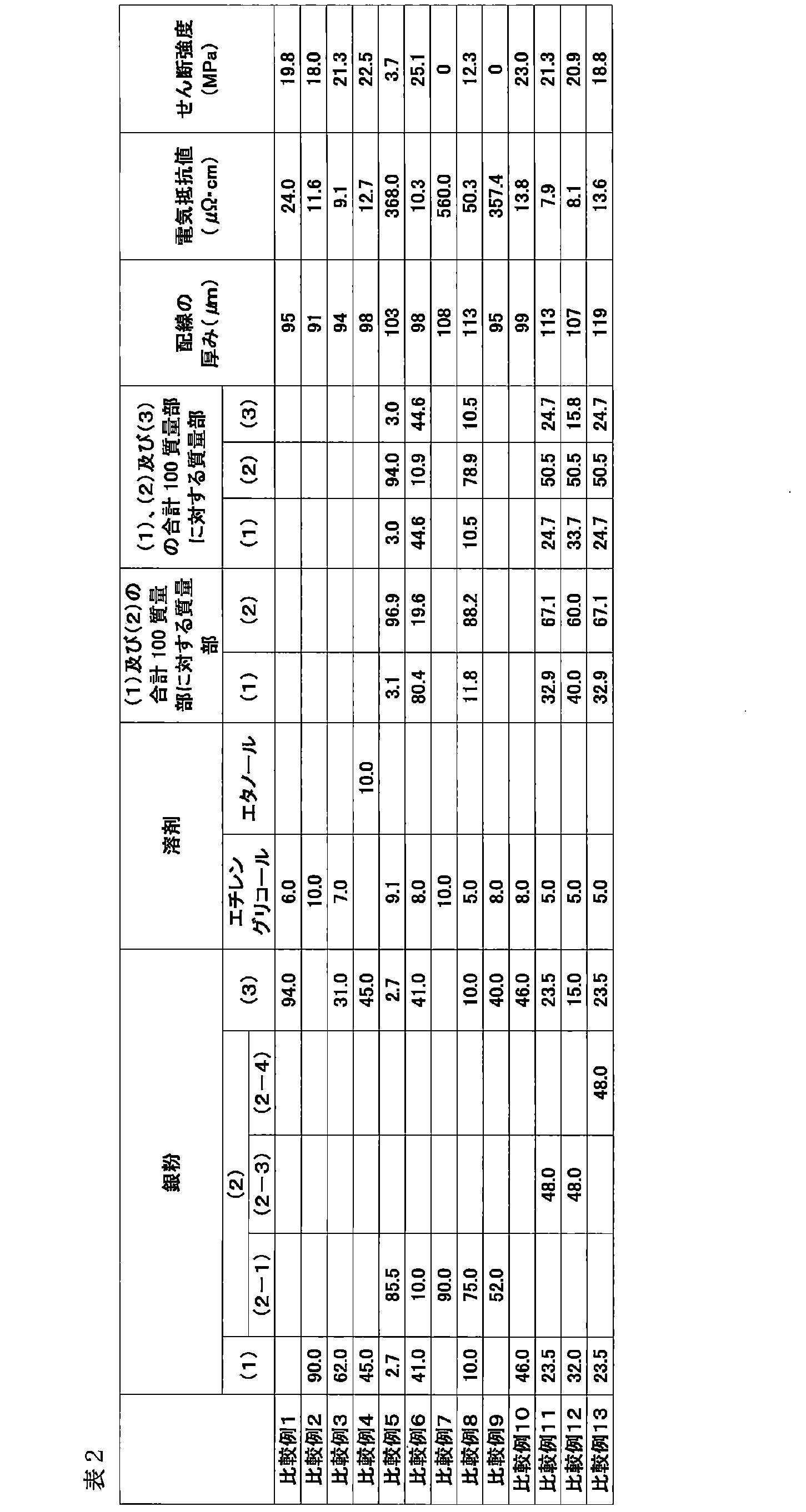
なお、以下の表1及び2中の各成分の数値は、導電性ペースト100質量部に対する各成分の質量部を表す。
以下の表1及び2に示す組成で実施例1~11並びに比較例1~13の導電性ペーストを調製した。
なお、以下の表1及び2中の各成分の数値は、導電性ペースト100質量部に対する各成分の質量部を表す。
そして、実施例1~11及び比較例1~13の導電性ペーストについて、上記の電気抵抗値及びせん断強度の評価を行った。評価結果を以下の表1及び2に示す。

実施例1~11の導電性ペーストは、15μm以下のメディアン径D50を有するフレーク状銀粉、25μm以上のメディアン径D50を有する銀粉、及び溶剤を含み、前記フレーク状銀粉と前記25μm以上のメディアン径D50を有する銀粉との合計100質量部に対して、前記フレーク状銀粉の含有量が15~70質量部であり、前記25μm以上のメディアン径D50を有する銀粉の含有量が30~85質量部である導電性ペーストである。
上記表1の結果より、実施例1~11の導電性ペーストにおいては、焼結体による配線の電気抵抗値が低く、良好な導電性を有し、また、焼結体がせん断強度に優れ、良好な接合性を有することがわかった。
上記表1の結果より、実施例1~11の導電性ペーストにおいては、焼結体による配線の電気抵抗値が低く、良好な導電性を有し、また、焼結体がせん断強度に優れ、良好な接合性を有することがわかった。
その中でも特に、実施例2及び3は、焼結体による配線の電気抵抗値が低く、より良好な導電性を有し、また、焼結体がせん断強度に優れ、より良好な接合性を有することがわかった。実施例2及び3は、フレーク状銀粉と25μm以上のメディアン径D50を有する銀粉との合計100質量部に対して、フレーク状銀粉の含有量が30~42質量部であり、25μm以上のメディアン径D50を有する銀粉の含有量が58~70質量部である導電性ペーストである。
一方、上記表2に示した比較例1は、銀粉(1)及び銀粉(2)を含まない導電性ペーストである。比較例2~4及び10は、銀粉(2)を含まない導電性ペーストである。また、比較例7及び9は、銀粉(1)を含まない導電性ペーストである。比較例5及び8は、銀粉(1)と銀粉(2-1)との両方を含むものの、銀粉(1)及び銀粉(2-1)の合計100質量部に対して、銀粉(1)の含有量が15質量部未満であり、銀粉(2-1)の含有量が85質量部を超える導電性ペーストである。また、比較例6は、銀粉(1)と銀粉(2-1)との両方を含むものの、銀粉(1)及び銀粉(2)の合計100質量部に対して、銀粉(1)の含有量が70質量部を超え、銀粉(2-1)の含有量が30質量部未満の導電性ペーストである。比較例11~13は、メディアン径D50が25μm以上である銀粉を含まない導電性ペーストである。
表2の結果からわかるように、比較例1~5、7~10、及び13の導電性ペーストは、実施例1~13の導電性ペーストに比べて、焼結体による配線の電気抵抗値が高く、導電性が不十分であり、また、焼結体のせん断強度が低く、接合性に劣っていた。比較例6の導電性ペーストは、焼結体が良好な接合性を有していたものの、焼結体による配線の電気抵抗値が高く、導電性が不十分であった。また、比較例11及び12の導電性ペーストは、焼結体による配線が良好な導電性を有していたものの、焼結体のせん断強度が低く、接合性に劣っていた。
実施例3、並びに比較例3及び7の焼結体による配線について、電界放出形走査電子顕微鏡(FE-SEM)(日本電子製 JSM-7000F)により撮影した画像を図4A~6Bに示す。
図4A、4C、及び4Dは、実施例3の配線の表面をそれぞれ倍率1000、5000、10000倍で撮影したものである。図4Bは、実施例3の配線の断面を倍率700倍で撮影したものである。
図5A、5C、及び5Dは、比較例3の配線の表面をそれぞれ倍率1000、5000、10000倍で撮影したものである。図5Bは、比較例3の配線の断面を倍率700倍で撮影したものである。
図6A及び6Bは、比較例7の配線の表面をそれぞれ倍率400、1000倍で撮影したものである。
図4A、4C、及び4Dは、実施例3の配線の表面をそれぞれ倍率1000、5000、10000倍で撮影したものである。図4Bは、実施例3の配線の断面を倍率700倍で撮影したものである。
図5A、5C、及び5Dは、比較例3の配線の表面をそれぞれ倍率1000、5000、10000倍で撮影したものである。図5Bは、比較例3の配線の断面を倍率700倍で撮影したものである。
図6A及び6Bは、比較例7の配線の表面をそれぞれ倍率400、1000倍で撮影したものである。
図4A~4Dより、実施例3の配線においては、径が小さくフレーク状の銀粉(1)、径の大きい銀粉(2-1)、及び径が小さく二峰性の粒度分布を有する銀粉(3)にそれぞれ由来する構造が焼結体において観察された。そして、実施例3の配線においては、フレーク状の銀粒子及び径の小さい銀粒子と径の大きい銀粒子とが互いに十分に接触し、かつ融合していることがわかった。これによって、実施例3の配線においては、配線内の電子の移動速度が大きくなり、電気抵抗値が低くなったと考えられる。
一方、図5A~5Dより、比較例3の配線においては、径が小さくフレーク状の銀粉(1)、及び径が小さく二峰性の粒度分布を有する銀粉(3)にそれぞれ由来する構造が焼結体において観察された。しかし、比較例3の配線においては、径の小さい銀粉(1)及び(3)のみで構成され、径の大きい銀粉(2-1)又は(2-2)を含まないため、銀粒子同士が一部接触しているものの、その他の部分では、銀粒子同士が十分に接触しておらず十分に融合していないことがわかった。これによって、比較例3の配線においては、実施例3の配線に比べて、電気抵抗値が高くなったと考えられる。
また、図6A及び6Bより、比較例7の配線においては、径の大きい銀粉(2-1)のみで構成され、径の小さな銀粉(1)及び(3)を含まないため、銀粒子それぞれが独立して存在しており銀粒子同士がほとんど融合していないことがわかった。これによって、比較例7の配線においては、電気抵抗値が極めて高くなったと考えられる。
また、実施例3及び比較例3の焼結後のせん断強度測定用試料について、電界放出形走査電子顕微鏡(FE-SEM)(日本電子製 JSM-7000F)により撮影した画像を図7A~8Bに示す。
図7A及び7Bは、実施例3の試料の断面をそれぞれ倍率1000、2500倍で撮影したものである。図8A及び8Bは、比較例3の試料の断面をそれぞれ倍率1000、2500倍で撮影したものである。
図7A及び7Bは、実施例3の試料の断面をそれぞれ倍率1000、2500倍で撮影したものである。図8A及び8Bは、比較例3の試料の断面をそれぞれ倍率1000、2500倍で撮影したものである。
図7A及び7Bより、実施例3の試料においては、径が小さくフレーク状の銀粉(1)、径の大きい銀粉(2-1)、及び径が小さく二峰性の粒度分布を有する銀粉(3)にそれぞれ由来する構造が焼結体において観察された。そして、実施例3の試料においては、フレーク状の銀粒子及び径の小さい銀粒子と径の大きい銀粒子とが互いに十分に接触及び融合し、焼結体内部の空隙が少ないことがわかった。これによって、実施例3の試料においては、焼結体が試験片に密着し、良好なせん断強度を示したと考えられる。
一方、図8A及び8Bより、比較例3の試料においては、径の小さな銀粉(1)及び(3)のみで構成され、径の大きい銀粉(2-1)又は(2-2)を含まないため、銀粒子同士が接触する面積が小さく十分に融合しないため、焼結体内部の空隙が多いことがわかった。これによって、比較例3の試料においては、実施例3の試料に比べて、せん断強度が低くなったと考えられる。
なお、図7A及び7Bと図8A及び8Bとの比較より、比較例3の試料においては、実施例3の試料に比べて、焼結体の部分の厚みが小さくなっていることがわかった。この原因について、チップマウンターを用いて試験片(2)を導電性ペーストの上に搭載する際に、チップマウンターのノズル荷重により、径の大きい銀粉(2-1)又は(2-2)を含まない比較例3は、導電性ペーストが押し潰され厚みが小さくなったと考えられる。また、比較例3は、径の大きい銀粉(2-1)又は(2-2)を含まず、より多くの溶剤を含むため、溶剤が焼結時に蒸発し収縮したと考えられる。
以上、表1及び2の結果より、15μm以下のメディアン径D50を有するフレーク状銀粉、25μm以上のメディアン径D50を有する銀粉、及び溶剤を含み、前記フレーク状銀粉と前記25μm以上のメディアン径D50を有する銀粉との合計100質量部に対して、前記フレーク状銀粉の含有量が15~70質量部であり、前記25μm以上のメディアン径D50を有する銀粉の含有量が30~85質量部である導電性ペーストを用いることにより、焼結体とした際の導電性に優れ、また、良好な接合性を示すことがわかった。
Claims (6)
- 15μm以下のメディアン径D50を有するフレーク状銀粉、25μm以上のメディアン径D50を有する銀粉、及び溶剤を含み、
前記フレーク状銀粉と前記25μm以上のメディアン径D50を有する銀粉との合計100質量部に対して、前記フレーク状銀粉の含有量が15~70質量部であり、前記25μm以上のメディアン径D50を有する銀粉の含有量が30~85質量部であることを特徴とする導電性ペースト。 - 15μm以下のメディアン径D50を有するフレーク状銀粉、25μm以上のメディアン径D50を有する銀粉、0.1μm~0.5μmと1μm~15μmとにピークを有する二峰性の粒度分布を有する銀粉、及び溶剤を含み、
前記フレーク状銀粉、前記25μm以上のメディアン径D50を有する銀粉、及び前記二峰性の粒度分布を有する銀粉の合計100質量部に対して、前記フレーク状銀粉の含有量が8~55質量部であり、前記25μm以上のメディアン径D50を有する銀粉の含有量が15~65質量部であり、前記二峰性の粒度分布を有する銀粉の含有量が4~45質量部であることを特徴とする導電性ペースト。 - 前記フレーク状銀粉と前記25μm以上のメディアン径D50を有する銀粉との合計100質量部に対して、前記フレーク状銀粉の含有量が30~42質量部であり、前記25μm以上のメディアン径D50を有する銀粉の含有量が58~70質量部であることを特徴とする請求項1に記載の導電性ペースト。
- 前記フレーク状銀粉、前記25μm以上のメディアン径D50を有する銀粉、及び前記二峰性の粒度分布を有する銀粉の合計100質量部に対して、前記フレーク状銀粉の含有量が23~35質量部であり、前記25μm以上のメディアン径D50を有する銀粉の含有量が40~63質量部であり、前記二峰性の粒度分布を有する銀粉の含有量が12~35質量部であることを特徴とする請求項2に記載の導電性ペースト。
- 請求項1~4のいずれか1つに記載の導電性ペーストを焼結してなる焼結体。
- 基板、請求項1~4のいずれか1つに記載の導電性ペースト、及び導電体を含む積層体を焼結してなる焼結体。
Priority Applications (5)
| Application Number | Priority Date | Filing Date | Title |
|---|---|---|---|
| US17/258,271 US11710580B2 (en) | 2018-07-06 | 2019-03-20 | Electrically conductive paste and sintered body |
| EP22193544.8A EP4148748B1 (en) | 2018-07-06 | 2019-03-20 | Electrically conductive paste and sintered body |
| CN201980039267.2A CN112272851B (zh) | 2018-07-06 | 2019-03-20 | 导电性糊料和烧结体 |
| JP2020528691A JP6756085B2 (ja) | 2018-07-06 | 2019-03-20 | 導電性ペースト及び焼結体 |
| EP19830980.9A EP3806111B1 (en) | 2018-07-06 | 2019-03-20 | Electrically conductive paste and sintered body |
Applications Claiming Priority (2)
| Application Number | Priority Date | Filing Date | Title |
|---|---|---|---|
| JP2018129163 | 2018-07-06 | ||
| JP2018-129163 | 2018-07-06 |
Publications (1)
| Publication Number | Publication Date |
|---|---|
| WO2020008689A1 true WO2020008689A1 (ja) | 2020-01-09 |
Family
ID=69060536
Family Applications (1)
| Application Number | Title | Priority Date | Filing Date |
|---|---|---|---|
| PCT/JP2019/011634 Ceased WO2020008689A1 (ja) | 2018-07-06 | 2019-03-20 | 導電性ペースト及び焼結体 |
Country Status (6)
| Country | Link |
|---|---|
| US (1) | US11710580B2 (ja) |
| EP (2) | EP3806111B1 (ja) |
| JP (1) | JP6756085B2 (ja) |
| CN (1) | CN112272851B (ja) |
| TW (1) | TWI729373B (ja) |
| WO (1) | WO2020008689A1 (ja) |
Cited By (3)
| Publication number | Priority date | Publication date | Assignee | Title |
|---|---|---|---|---|
| JP2021091819A (ja) * | 2019-12-12 | 2021-06-17 | スタンレー電気株式会社 | 焼結用インク、その製造方法、金属粒子、その製造方法、および、回路基板の製造方法 |
| CN113168931A (zh) * | 2020-06-24 | 2021-07-23 | 千住金属工业株式会社 | 导电性糊料、层叠体及Cu基板或Cu电极与导电体的接合方法 |
| WO2021260960A1 (ja) | 2020-06-24 | 2021-12-30 | 千住金属工業株式会社 | 導電性ペースト、積層体、及びCu基板又はCu電極と導電体との接合方法 |
Families Citing this family (1)
| Publication number | Priority date | Publication date | Assignee | Title |
|---|---|---|---|---|
| EP4324578B1 (de) * | 2022-08-17 | 2024-10-09 | Heraeus Electronics GmbH & Co. KG | Silbersinterpaste und deren verwendung zum verbinden von bauelementen |
Citations (5)
| Publication number | Priority date | Publication date | Assignee | Title |
|---|---|---|---|---|
| JPH0581923A (ja) | 1991-01-31 | 1993-04-02 | Fukuda Metal Foil & Powder Co Ltd | 導電性接着剤 |
| JP2004362950A (ja) | 2003-06-05 | 2004-12-24 | Noritake Co Ltd | 銀粉末を主体とする導体ペースト及びその製造方法 |
| WO2007034833A1 (ja) | 2005-09-21 | 2007-03-29 | Nihon Handa Co., Ltd. | ペースト状銀粒子組成物、固形状銀の製造方法、固形状銀、接合方法およびプリント配線板の製造方法 |
| JP2009170277A (ja) | 2008-01-17 | 2009-07-30 | Osaka Univ | 導電性ペースト |
| JP2012028250A (ja) * | 2010-07-27 | 2012-02-09 | Jsr Corp | 導電性ペースト組成物および導電接着方法 |
Family Cites Families (10)
| Publication number | Priority date | Publication date | Assignee | Title |
|---|---|---|---|---|
| US6814795B2 (en) * | 2001-11-27 | 2004-11-09 | Ferro Corporation | Hot melt conductor paste composition |
| JP4790238B2 (ja) | 2004-08-27 | 2011-10-12 | 鬼怒川ゴム工業株式会社 | 導電性弾性体組成物 |
| JP5281529B2 (ja) * | 2009-09-28 | 2013-09-04 | 京都エレックス株式会社 | 加熱硬化型導電性ペースト組成物およびその導電性ペースト組成物を用いた電極並びに配線パターンの形成方法 |
| SG188359A1 (en) * | 2010-09-01 | 2013-04-30 | Ferro Corp | Via fill material for solar applications |
| US8419981B2 (en) * | 2010-11-15 | 2013-04-16 | Cheil Industries, Inc. | Conductive paste composition and electrode prepared using the same |
| WO2012133627A1 (ja) * | 2011-03-31 | 2012-10-04 | 戸田工業株式会社 | 銀コート銅粉及びその製造法、該銀コート銅粉を含有する導電性ペースト、導電性接着剤、導電性膜、及び電気回路 |
| CN103000248B (zh) * | 2012-11-10 | 2015-10-28 | 江苏瑞德新能源科技有限公司 | 一种适应高方阻浅结的太阳能电池正银浆料用粉体料 |
| US8828536B2 (en) * | 2013-02-04 | 2014-09-09 | Eastman Kodak Company | Conductive article having silver nanoparticles |
| WO2016007351A1 (en) * | 2014-07-11 | 2016-01-14 | E. I. Du Pont De Nemours And Company | Flowable compositions with low temperature curing to form thermally conductive pathways in electronics type applications and methods relating thereto |
| EP3381047A4 (en) * | 2015-11-24 | 2019-07-03 | Hitachi Chemical Co., Ltd. | BURNED MULTILAYER STACKS IN INTEGRATED CIRCUITS AND SOLAR CELLS |
-
2019
- 2019-03-20 CN CN201980039267.2A patent/CN112272851B/zh active Active
- 2019-03-20 JP JP2020528691A patent/JP6756085B2/ja active Active
- 2019-03-20 EP EP19830980.9A patent/EP3806111B1/en active Active
- 2019-03-20 US US17/258,271 patent/US11710580B2/en active Active
- 2019-03-20 EP EP22193544.8A patent/EP4148748B1/en active Active
- 2019-03-20 WO PCT/JP2019/011634 patent/WO2020008689A1/ja not_active Ceased
- 2019-04-01 TW TW108111518A patent/TWI729373B/zh active
Patent Citations (5)
| Publication number | Priority date | Publication date | Assignee | Title |
|---|---|---|---|---|
| JPH0581923A (ja) | 1991-01-31 | 1993-04-02 | Fukuda Metal Foil & Powder Co Ltd | 導電性接着剤 |
| JP2004362950A (ja) | 2003-06-05 | 2004-12-24 | Noritake Co Ltd | 銀粉末を主体とする導体ペースト及びその製造方法 |
| WO2007034833A1 (ja) | 2005-09-21 | 2007-03-29 | Nihon Handa Co., Ltd. | ペースト状銀粒子組成物、固形状銀の製造方法、固形状銀、接合方法およびプリント配線板の製造方法 |
| JP2009170277A (ja) | 2008-01-17 | 2009-07-30 | Osaka Univ | 導電性ペースト |
| JP2012028250A (ja) * | 2010-07-27 | 2012-02-09 | Jsr Corp | 導電性ペースト組成物および導電接着方法 |
Non-Patent Citations (1)
| Title |
|---|
| See also references of EP3806111A4 |
Cited By (10)
| Publication number | Priority date | Publication date | Assignee | Title |
|---|---|---|---|---|
| JP2021091819A (ja) * | 2019-12-12 | 2021-06-17 | スタンレー電気株式会社 | 焼結用インク、その製造方法、金属粒子、その製造方法、および、回路基板の製造方法 |
| CN113168931A (zh) * | 2020-06-24 | 2021-07-23 | 千住金属工业株式会社 | 导电性糊料、层叠体及Cu基板或Cu电极与导电体的接合方法 |
| KR102307809B1 (ko) | 2020-06-24 | 2021-09-30 | 센주긴조쿠고교 가부시키가이샤 | 도전성 페이스트, 적층체, 및 Cu 기판 또는 Cu 전극과 도전체와의 접합 방법 |
| WO2021260960A1 (ja) | 2020-06-24 | 2021-12-30 | 千住金属工業株式会社 | 導電性ペースト、積層体、及びCu基板又はCu電極と導電体との接合方法 |
| US11278955B2 (en) | 2020-06-24 | 2022-03-22 | Senju Metal Industry Co., Ltd. | Electrically conductive paste, laminated body, and method for bonding Cu substrate or Cu electrode to electrical conductor |
| EP3958279A4 (en) * | 2020-06-24 | 2022-09-14 | Senju Metal Industry Co., Ltd | CONDUCTIVE PASTE, LAMINATE BODY, METHOD OF CONNECTING COPPER LAMINATE/COPPER ELECTRODE AND CONDUCTOR |
| EP4279265A2 (en) | 2020-06-24 | 2023-11-22 | Senju Metal Industry Co., Ltd. | Conductive paste, laminate body, method of bonding copper laminate/copper electrode and conductor |
| EP4279264A2 (en) | 2020-06-24 | 2023-11-22 | Senju Metal Industry Co., Ltd. | Conductive paste, laminate body, method of bonding copper laminate/copper electrode and conductor |
| EP4279264A3 (en) * | 2020-06-24 | 2024-02-21 | Senju Metal Industry Co., Ltd. | Conductive paste, laminate body, method of bonding copper laminate/copper electrode and conductor |
| EP4279265A3 (en) * | 2020-06-24 | 2024-02-21 | Senju Metal Industry Co., Ltd. | Conductive paste, laminate body, method of bonding copper laminate/copper electrode and conductor |
Also Published As
| Publication number | Publication date |
|---|---|
| EP3806111B1 (en) | 2024-03-13 |
| JPWO2020008689A1 (ja) | 2020-12-17 |
| JP6756085B2 (ja) | 2020-09-16 |
| TWI729373B (zh) | 2021-06-01 |
| US11710580B2 (en) | 2023-07-25 |
| EP3806111A1 (en) | 2021-04-14 |
| TW202006749A (zh) | 2020-02-01 |
| EP4148748A1 (en) | 2023-03-15 |
| CN112272851B (zh) | 2022-03-01 |
| EP3806111A4 (en) | 2021-08-11 |
| CN112272851A (zh) | 2021-01-26 |
| US20210245242A1 (en) | 2021-08-12 |
| EP4148748B1 (en) | 2025-07-09 |
Similar Documents
| Publication | Publication Date | Title |
|---|---|---|
| JP4353380B2 (ja) | ペースト状銀粒子組成物、固形状銀の製造方法、固形状銀、接合方法およびプリント配線板の製造方法 | |
| JP6756085B2 (ja) | 導電性ペースト及び焼結体 | |
| CN1665899A (zh) | 导电性粘接剂及使用它的电路 | |
| US11278955B2 (en) | Electrically conductive paste, laminated body, and method for bonding Cu substrate or Cu electrode to electrical conductor | |
| KR20120004122A (ko) | 전도성 페이스트 및 이를 이용한 전극 | |
| US12257622B2 (en) | Joining material, production method for joining material, and joined body | |
| JP6778389B1 (ja) | 導電性ペースト、積層体、及びCu基板又はCu電極と導電体との接合方法 | |
| JP7317397B2 (ja) | 酸化銅ペースト及び電子部品の製造方法 | |
| CN114845827A (zh) | 银膏及其制造方法以及接合体的制造方法 | |
| HK40086695A (en) | Electrically conductive paste and sintered body | |
| HK40086695B (en) | Electrically conductive paste and sintered body | |
| HK40103214B (en) | Conductive paste, laminate body, method of bonding copper laminate/copper electrode and conductor | |
| HK40103214A (en) | Conductive paste, laminate body, method of bonding copper laminate/copper electrode and conductor | |
| HK40102045A (en) | Conductive paste, laminate body, method of bonding copper laminate/copper electrode and conductor | |
| HK40102045B (en) | Conductive paste, laminate body, method of bonding copper laminate/copper electrode and conductor | |
| TWI789698B (zh) | 氧化銅糊料及電子零件之製造方法 | |
| WO2026058762A1 (ja) | 焼結性接合用ペースト及び接合構造体 | |
| WO2026058964A1 (ja) | 銅ペースト |
Legal Events
| Date | Code | Title | Description |
|---|---|---|---|
| 121 | Ep: the epo has been informed by wipo that ep was designated in this application |
Ref document number: 19830980 Country of ref document: EP Kind code of ref document: A1 |
|
| WWE | Wipo information: entry into national phase |
Ref document number: 2020528691 Country of ref document: JP |
|
| NENP | Non-entry into the national phase |
Ref country code: DE |
|
| ENP | Entry into the national phase |
Ref document number: 2019830980 Country of ref document: EP Effective date: 20210106 |