WO2020008618A1 - 内視鏡用撮像装置、および、内視鏡 - Google Patents
内視鏡用撮像装置、および、内視鏡 Download PDFInfo
- Publication number
- WO2020008618A1 WO2020008618A1 PCT/JP2018/025671 JP2018025671W WO2020008618A1 WO 2020008618 A1 WO2020008618 A1 WO 2020008618A1 JP 2018025671 W JP2018025671 W JP 2018025671W WO 2020008618 A1 WO2020008618 A1 WO 2020008618A1
- Authority
- WO
- WIPO (PCT)
- Prior art keywords
- imaging device
- optical
- endoscope
- lens
- resin
- Prior art date
- Legal status (The legal status is an assumption and is not a legal conclusion. Google has not performed a legal analysis and makes no representation as to the accuracy of the status listed.)
- Ceased
Links
Images







Classifications
-
- H—ELECTRICITY
- H04—ELECTRIC COMMUNICATION TECHNIQUE
- H04N—PICTORIAL COMMUNICATION, e.g. TELEVISION
- H04N23/00—Cameras or camera modules comprising electronic image sensors; Control thereof
- H04N23/50—Constructional details
- H04N23/55—Optical parts specially adapted for electronic image sensors; Mounting thereof
-
- H—ELECTRICITY
- H10—SEMICONDUCTOR DEVICES; ELECTRIC SOLID-STATE DEVICES NOT OTHERWISE PROVIDED FOR
- H10F—INORGANIC SEMICONDUCTOR DEVICES SENSITIVE TO INFRARED RADIATION, LIGHT, ELECTROMAGNETIC RADIATION OF SHORTER WAVELENGTH OR CORPUSCULAR RADIATION
- H10F39/00—Integrated devices, or assemblies of multiple devices, comprising at least one element covered by group H10F30/00, e.g. radiation detectors comprising photodiode arrays
- H10F39/80—Constructional details of image sensors
- H10F39/804—Containers or encapsulations
-
- A—HUMAN NECESSITIES
- A61—MEDICAL OR VETERINARY SCIENCE; HYGIENE
- A61B—DIAGNOSIS; SURGERY; IDENTIFICATION
- A61B1/00—Instruments for performing medical examinations of the interior of cavities or tubes of the body by visual or photographical inspection, e.g. endoscopes; Illuminating arrangements therefor
- A61B1/00064—Constructional details of the endoscope body
- A61B1/00071—Insertion part of the endoscope body
- A61B1/0008—Insertion part of the endoscope body characterised by distal tip features
- A61B1/00096—Optical elements
-
- A—HUMAN NECESSITIES
- A61—MEDICAL OR VETERINARY SCIENCE; HYGIENE
- A61B—DIAGNOSIS; SURGERY; IDENTIFICATION
- A61B1/00—Instruments for performing medical examinations of the interior of cavities or tubes of the body by visual or photographical inspection, e.g. endoscopes; Illuminating arrangements therefor
- A61B1/00064—Constructional details of the endoscope body
- A61B1/0011—Manufacturing of endoscope parts
-
- A—HUMAN NECESSITIES
- A61—MEDICAL OR VETERINARY SCIENCE; HYGIENE
- A61B—DIAGNOSIS; SURGERY; IDENTIFICATION
- A61B1/00—Instruments for performing medical examinations of the interior of cavities or tubes of the body by visual or photographical inspection, e.g. endoscopes; Illuminating arrangements therefor
- A61B1/00163—Optical arrangements
-
- A—HUMAN NECESSITIES
- A61—MEDICAL OR VETERINARY SCIENCE; HYGIENE
- A61B—DIAGNOSIS; SURGERY; IDENTIFICATION
- A61B1/00—Instruments for performing medical examinations of the interior of cavities or tubes of the body by visual or photographical inspection, e.g. endoscopes; Illuminating arrangements therefor
- A61B1/04—Instruments for performing medical examinations of the interior of cavities or tubes of the body by visual or photographical inspection, e.g. endoscopes; Illuminating arrangements therefor combined with photographic or television appliances
- A61B1/05—Instruments for performing medical examinations of the interior of cavities or tubes of the body by visual or photographical inspection, e.g. endoscopes; Illuminating arrangements therefor combined with photographic or television appliances characterised by the image sensor, e.g. camera, being in the distal end portion
-
- A—HUMAN NECESSITIES
- A61—MEDICAL OR VETERINARY SCIENCE; HYGIENE
- A61B—DIAGNOSIS; SURGERY; IDENTIFICATION
- A61B1/00—Instruments for performing medical examinations of the interior of cavities or tubes of the body by visual or photographical inspection, e.g. endoscopes; Illuminating arrangements therefor
- A61B1/04—Instruments for performing medical examinations of the interior of cavities or tubes of the body by visual or photographical inspection, e.g. endoscopes; Illuminating arrangements therefor combined with photographic or television appliances
- A61B1/05—Instruments for performing medical examinations of the interior of cavities or tubes of the body by visual or photographical inspection, e.g. endoscopes; Illuminating arrangements therefor combined with photographic or television appliances characterised by the image sensor, e.g. camera, being in the distal end portion
- A61B1/051—Details of CCD assembly
-
- G—PHYSICS
- G02—OPTICS
- G02B—OPTICAL ELEMENTS, SYSTEMS OR APPARATUS
- G02B13/00—Optical objectives specially designed for the purposes specified below
- G02B13/001—Miniaturised objectives for electronic devices, e.g. portable telephones, webcams, PDAs, small digital cameras
- G02B13/0085—Miniaturised objectives for electronic devices, e.g. portable telephones, webcams, PDAs, small digital cameras employing wafer level optics
-
- G—PHYSICS
- G02—OPTICS
- G02B—OPTICAL ELEMENTS, SYSTEMS OR APPARATUS
- G02B23/00—Telescopes, e.g. binoculars; Periscopes; Instruments for viewing the inside of hollow bodies; Viewfinders; Optical aiming or sighting devices
- G02B23/24—Instruments or systems for viewing the inside of hollow bodies, e.g. fibrescopes
- G02B23/2407—Optical details
- G02B23/2423—Optical details of the distal end
- G02B23/243—Objectives for endoscopes
-
- H—ELECTRICITY
- H04—ELECTRIC COMMUNICATION TECHNIQUE
- H04N—PICTORIAL COMMUNICATION, e.g. TELEVISION
- H04N25/00—Circuitry of solid-state image sensors [SSIS]; Control thereof
- H04N25/70—SSIS architectures; Circuits associated therewith
-
- H—ELECTRICITY
- H10—SEMICONDUCTOR DEVICES; ELECTRIC SOLID-STATE DEVICES NOT OTHERWISE PROVIDED FOR
- H10F—INORGANIC SEMICONDUCTOR DEVICES SENSITIVE TO INFRARED RADIATION, LIGHT, ELECTROMAGNETIC RADIATION OF SHORTER WAVELENGTH OR CORPUSCULAR RADIATION
- H10F39/00—Integrated devices, or assemblies of multiple devices, comprising at least one element covered by group H10F30/00, e.g. radiation detectors comprising photodiode arrays
- H10F39/80—Constructional details of image sensors
- H10F39/806—Optical elements or arrangements associated with the image sensors
-
- H—ELECTRICITY
- H10—SEMICONDUCTOR DEVICES; ELECTRIC SOLID-STATE DEVICES NOT OTHERWISE PROVIDED FOR
- H10F—INORGANIC SEMICONDUCTOR DEVICES SENSITIVE TO INFRARED RADIATION, LIGHT, ELECTROMAGNETIC RADIATION OF SHORTER WAVELENGTH OR CORPUSCULAR RADIATION
- H10F39/00—Integrated devices, or assemblies of multiple devices, comprising at least one element covered by group H10F30/00, e.g. radiation detectors comprising photodiode arrays
- H10F39/80—Constructional details of image sensors
- H10F39/806—Optical elements or arrangements associated with the image sensors
- H10F39/8063—Microlenses
-
- G—PHYSICS
- G02—OPTICS
- G02B—OPTICAL ELEMENTS, SYSTEMS OR APPARATUS
- G02B23/00—Telescopes, e.g. binoculars; Periscopes; Instruments for viewing the inside of hollow bodies; Viewfinders; Optical aiming or sighting devices
- G02B23/24—Instruments or systems for viewing the inside of hollow bodies, e.g. fibrescopes
- G02B23/2476—Non-optical details, e.g. housings, mountings, supports
- G02B23/2484—Arrangements in relation to a camera or imaging device
-
- H—ELECTRICITY
- H04—ELECTRIC COMMUNICATION TECHNIQUE
- H04N—PICTORIAL COMMUNICATION, e.g. TELEVISION
- H04N23/00—Cameras or camera modules comprising electronic image sensors; Control thereof
- H04N23/50—Constructional details
- H04N23/555—Constructional details for picking-up images in sites, inaccessible due to their dimensions or hazardous conditions, e.g. endoscopes or borescopes
Definitions
- the present invention relates to an endoscope imaging device including an optical unit including a resin lens, and an endoscope including an endoscope imaging device including an optical unit including a resin lens.
- Japanese Patent Application Laid-Open No. 2012-18993 discloses an imaging module including a wafer-level laminated body. This imaging module is manufactured by bonding an optical wafer including a plurality of optical elements and an imaging wafer including a plurality of imaging elements, and then cutting the wafer into individual pieces.
- Japanese Patent Application Laid-Open No. 2015-38538 discloses a so-called hybrid lens element in which a lens made of resin is provided on a parallel flat glass plate.
- the resin lens of the hybrid lens element has higher moisture permeability than the glass lens.
- the endoscope is used in a high-humidity environment or is subjected to an autoclave process (high-temperature high-pressure steam process). For this reason, when an imaging device including a hybrid lens element is used for an endoscope, the resin lens absorbs moisture, which may cause a change in shape or fogging, thereby deteriorating optical characteristics.
- An object of the embodiments of the present invention is to provide a small endoscope imaging device excellent in moisture resistance and a minimally invasive endoscope excellent in moisture resistance.
- a plurality of optical elements are joined, and at least one of the plurality of optical elements is provided with a resin lens on a main surface of a parallel flat glass plate.
- the main surface around the resin lens and the resin lens is a transparent inorganic film.
- An endoscope of another embodiment includes an endoscope imaging device, wherein the endoscope imaging device has a plurality of optical elements joined thereto, and at least one of the plurality of optical elements is a parallel plate.
- An optical unit that is a hybrid lens element in which a resin lens is disposed on a main surface of a glass plate, and an imaging unit that receives a subject image condensed by the optical unit, and the surface of the resin lens and the The main surface around the resin lens is covered with a transparent inorganic film.
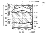
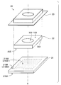
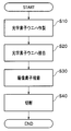
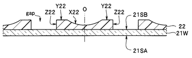
- FIG. 3 is a cross-sectional view of the imaging device for an endoscope according to the embodiment, taken along line III-III of FIG. 2. It is an exploded view of the optical element of the imaging device for endoscopes of the embodiment. It is a flow chart for explaining the manufacturing method of the imaging device for endoscopes of an embodiment. It is sectional drawing of the optical element wafer for demonstrating the manufacturing method of the imaging device for endoscopes of embodiment. It is sectional drawing of the optical element wafer for demonstrating the manufacturing method of the imaging device for endoscopes of embodiment.
- FIG. 3 is an exploded cross-sectional view of a bonded wafer for describing a method of manufacturing the imaging device for an endoscope according to the embodiment. It is sectional drawing of the joining wafer for demonstrating the manufacturing method of the imaging device for endoscopes of embodiment. It is sectional drawing of the joining wafer for demonstrating the manufacturing method of the imaging device for endoscopes of embodiment. It is sectional drawing of the joining wafer for demonstrating the manufacturing method of the imaging device for endoscopes of embodiment. It is sectional drawing of the imaging device for endoscopes of the modification 1 of embodiment.
- an endoscope system 8 including the endoscope 9 of the embodiment includes the endoscope 9, a processor 80, a light source device 81, and a monitor 82.
- the endoscope 9 has the insertion unit 90 inserted into the body cavity of the subject, captures an in-vivo image of the subject, and outputs an imaging signal.
- the insertion portion 90 includes a rigid distal end portion 90A in which the imaging device 1 for an endoscope (hereinafter, referred to as an “imaging device 1”) is disposed, and a freely bendable connected to a proximal end portion of the rigid distal end portion 90A.
- the bending portion 90B includes a flexible portion 90B and a flexible portion 90C connected to the base end of the bending portion 90B.
- the bending section 90 ⁇ / b> B is bent by the operation of the operation section 91.
- the universal cord 92 extending from the operation unit 91 is connected to the processor 80 and the light source device 81 via the connector 93.
- a signal cable 94 that transmits an electric signal output by the imaging device 1 is inserted through the insertion unit 90, the operation unit 91, and the universal cord 92.
- the processor 80 controls the entire endoscope system 8, performs signal processing on an image signal output from the image capturing apparatus 1, and outputs the image signal as an image signal.
- the monitor 82 displays an image signal output by the processor 80.
- the light source device 81 has, for example, a white LED.
- the illumination light emitted from the light source device 81 is guided to the rigid distal end portion 90A via a light guide (not shown) passing through the universal cord 92 and the insertion portion 90, and illuminates the subject.
- the imaging device 1 of the endoscope 9 is small and excellent in moisture resistance as described later, the endoscope 9 is minimally invasive and excellent in moisture resistance.
- the endoscope 9 is a medical flexible endoscope
- the endoscope according to another embodiment may be a rigid endoscope or an industrial endoscope.
- the imaging device 1 for an endoscope includes an optical unit 10 and an imaging unit 50.
- the optical unit 10 is a wafer-level laminate in which a plurality of optical elements 20, 29, 30, 39, 40, and 49 are joined. That is, since the optical unit 10 is manufactured by cutting the bonded wafer 10W (see FIG. 10) in which a plurality of optical element wafers are bonded, there is a cut mark on the side surface 10SS, and the outer dimensions in the optical axis orthogonal direction are the same or substantially the same. (For example, within ⁇ 5% of the average outer dimension).
- the optical elements 20, 30, and 40 are hybrid lens elements in which resin lenses 22, 32, and 42 are disposed on parallel flat glass plates (hereinafter, referred to as "glass plates") 21, 31, and 41, respectively.
- the lens transparent resin constituting the resin lenses 22, 32, 42 is, for example, an acrylic resin.
- the imaging unit 50 including the imaging element 51 and the cover glass 52 has the cover glass 52 joined to the optical unit 10 and receives the subject image condensed by the optical unit 10.
- the intervals between the plurality of optical elements 20, 30, 40 and the imaging unit 50 are defined by the optical elements 29, 39, 49, which are spacer elements, respectively.
- the optical elements 29, 39, and 49 are made of, for example, silicon, and a region constituting an optical path is a space.
- the optical elements 29, 39, and 49 may be glass having a predetermined shape.
- the optical element 20 is a hybrid lens element in which an aspheric concave lens 22 made of resin is disposed on a second main surface 21SB of a glass plate 21 having a first main surface 21SA and a second main surface 21SB. is there.
- the first main surface 21SA is the front surface 10SA of the optical unit 10.
- the optical element 30 is a hybrid lens element in which an aspherical convex lens 32 made of resin is disposed on a third main surface 31SA of a glass plate 31 having a third main surface 31SA and a fourth main surface 31SB. is there.
- the optical element 40 is a hybrid lens element in which an aspheric convex lens 42 made of resin is disposed on a sixth main surface 41SB of a glass plate 41 having a fifth main surface 41SA and a sixth main surface 41SB. is there.
- the configuration of the optical unit 10, that is, the type and number of the optical elements and the stacking order can be variously modified according to the specifications.
- a patterned light-shielding film having a diaphragm function may be provided on the main surface of the optical element.
- the entire surfaces of all the resin lenses 22, 32, and the main surfaces 21SB, 31SA, and 41SB around all the resin lenses 22, 32, and 42 are formed of the transparent inorganic film 23 made of a transparent inorganic material. , 33, 43.
- the side surface 10SS of the optical unit 10 is not exposed to the outside.
- the front surface 10SA of the optical unit 10 (the first main surface 21SA of the optical element 20) is exposed. Even if covered with a transparent inorganic film, the reliability of the resin lens is not sufficient compared to the glass lens. Moreover, the exposed resin lens may be damaged.
- the imaging device 1 has high reliability because no resin lens is provided on the front surface (first main surface 20SA) of the optical element 20.
- the resin lens 22, which is a concave lens, has a transparent inorganic film 23 covering a surface composed of a concave optical path surface X22 constituting an optical path, an outer peripheral surface Y22 surrounding the optical path surface X22, and an outer surface Z22.
- the joint surface A22 facing the optical path surface X22 and the outer peripheral surface Y22 is integrally formed with the second main surface 21SB1 (21SB) of the glass plate 21.
- the second principal surface 21SB2 (21SB) around the resin lens 22 is also provided. It is covered with a transparent inorganic film 23.
- the outer surface Z22 which is the peripheral portion of the outer peripheral surface Y22, which is the starting point of peeling, is covered with the transparent inorganic film 23 disposed over the second main surface 21SB (21SB2). Therefore, the joining reliability is high.
- the optical element 30 which is a convex lens, has the entire surface of the resin lens 32 and the third main surface 31 SA around the resin lens 32 covered with the transparent inorganic film 33. I have.
- the optical element 40 which is a convex lens, the entire surface of the resin lens 42 and the sixth main surface 41SB around the resin lens 42 are covered with the transparent inorganic film 43.
- Direct bonding is performed by, for example, performing vacuum plasma processing to remove contamination on the surface that is the bonding surface or performing activation processing to form a dangling bond, and press-bonding the activated surfaces to each other. This is a technology for bonding substrates. After bonding at room temperature, the bonding strength can be further increased by heat treatment. For direct bonding, a metal film or an inorganic film such as silicon oxide may be formed on the bonding surface.
- the imaging device 1 is small because it includes the optical unit 10 made of a wafer-level laminate. Further, since the resin lenses 22, 32, and 42 are covered with the transparent inorganic film 43 having low moisture permeability, they have excellent moisture resistance.
- the endoscope 9 including the imaging device 1 is minimally invasive and has excellent moisture resistance.
- the junction between the optical unit 10 and the imaging unit 50 and the junction between the imaging element 51 and the cover glass 52 do not contain an organic material having high moisture permeability.
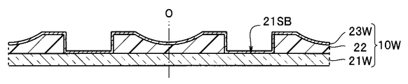
- Optical Element Wafer Manufacturing Step For example, as shown in FIG. 6, a glass wafer 21W that is a parallel plate glass is prepared. The thickness of the glass wafer 21 ⁇ / b> W is determined according to the specifications of the imaging device 1. When the glass wafer 21W is cut, it becomes the glass plate 21 of the optical element 20.
- a plurality of resin lenses 22 are arranged at predetermined positions on the second main surface 20SB of the glass wafer 21W. For example, by applying a transparent resin for a lens and pressing a mold (not shown) having a predetermined shape against the second main surface 21SB, ultraviolet rays (UV) are irradiated from the direction of the first main surface 21SA. When the transparent resin for the lens is cured, the molded resin lens 22 is disposed on the second main surface 21SB.
- UV ultraviolet rays
- the resin lens 22 is a concave lens, and its surfaces are an optical path surface X22, an outer peripheral surface Y22 surrounding the optical path surface X22, and an outer surface Z22.
- the plurality of resin lenses 22 have an outer peripheral surface Y22 that is separated from the outer peripheral surface Y22 of each of the resin lenses 22 with a gap therebetween.
- a silicon oxide (SiO 2 ) film is formed as a transparent inorganic film 23W on the entire surface of the second main surface 21SB of the glass wafer 21W provided with the plurality of resin lenses 22. That is, the transparent inorganic film 23W covers the entire surface of the plurality of resin lenses 22 and the second main surface 20SB of the glass wafer 21W around the plurality of resin lenses 22.
- the transparent inorganic film preferably has a moisture permeability of 5 g / (m 2 ⁇ day) or less in a water vapor permeability test defined in JIS Z 0208, even in a region where the film thickness is the smallest, and is preferably 1 g / (m 2). ⁇ day) or less. Further, the transparent inorganic film preferably has a transmittance of 90% or more at the wavelength of the light to be collected. Further, the film thickness on the optical path plane X22 is preferably 0.1 ⁇ m or more and 10 ⁇ m or less, and the film thickness variation is preferably within ⁇ 10% of the film thickness.
- the film thickness is not less than the above range, the effect of improving moisture permeability is ensured.
- the film thickness and the film thickness variation are less than the above ranges, the surface of the resin lens 22, particularly the shape of the optical path plane X22 does not change, so that the optical characteristics do not deteriorate.
- the transparent inorganic film 23W may be a multilayer film including a plurality of transparent inorganic layers as long as it has the above characteristics.
- the transparent inorganic film 23W is made of aluminum oxide (Al 2 O 3 ), silicon nitride (SiN), magnesium oxide (MgO), niobium oxide (Nb 2 O 5 ), silicon oxide (SiO 2 ), and tantalum oxide (Ta 2 ). O 5 ), at least one of titanium oxide (TiO 2 ), zirconium oxide (ZrO 2 ), magnesium fluoride (MgF 2 ), antimony sulfide (Sb 2 S 3 ), and zinc sulfide (ZnS), or , A multilayer film made of a plurality of materials.
- the transparent inorganic film 23W is preferably formed at a temperature equal to or lower than the softening point of the resin lens 22, for example, at 100 ° C. to 200 ° C. in order to prevent the resin lens 22 from being deteriorated and deformed.
- the transparent inorganic film 23W is provided by, for example, a CVD method, a sputtering method, a vapor deposition method, or a dehydration condensation method such as alkoxysilane (water glass).
- the optical element wafer 20W is manufactured by disposing the plurality of resin lenses 22 on the glass wafer 21W and forming the transparent inorganic film 23W covering the resin lenses 22.
- an optical element wafer 30W is manufactured by disposing a plurality of resin lenses 32 on a glass wafer 31W and forming a transparent inorganic film 33W covering the resin lenses 32 (see FIG. 10).
- an optical element wafer 40W is manufactured (see FIG. 10).
- the optical element wafers 20W, 30W, and 40W may have resin lenses 22, 32, and 42 formed of different resins, or may have different transparent inorganic films 23W, 33W, and 43W formed thereon.
- an etching mask 28 for forming a space serving as an optical path is provided on the main surface of the silicon wafer 29W.
- a support substrate 27 is bonded to a main surface (back surface) opposite to the main surface on which the etching mask 28 is provided.
- an optical element wafer which is a spacer wafer having a plurality of through-holes H29, which is a space serving as an optical path, by dry etching using an ICP-RIE method or the like or wet etching using an alkaline solution such as KOH or TMAH. 29W is produced.
- the through hole H29 may be formed by a physical processing method such as laser processing.
- the inner diameter of the through hole H29 in the direction orthogonal to the optical axis is set slightly larger than the outer diameter of the outer peripheral surface Y22 of the resin lens 22.
- Optical element wafers 39W and 49W to be a plurality of spacers 39 and 49 are manufactured by the same method as the optical element wafer 29W (see FIG. 10).
- the material of the optical element wafers 29W, 39W, and 49W is not limited to silicon, but may be ceramic, glass, metal, or resin as described later. Note that, for direct bonding, a silicon oxide film or the like is formed on the main surface of a wafer made of metal or resin.
- the transparent inorganic film 23W may be formed.
- the plurality of image pickup units 50 are bonded to the bonded wafer 10W by a bonding layer (not shown).
- a light receiving unit 53 such as a CMOS light receiving element is provided on the light receiving surface 50SA by a known semiconductor manufacturing method for a semiconductor wafer. Then, by producing a through wiring (not shown), an imaging element wafer (not shown) in which the light receiving portion 53 and the external connection electrode 54 on the back surface 50SB are connected is produced. After the glass wafer is joined to the light receiving surface 50SA of the imaging element wafer by an adhesive layer (not shown) and then cut, the imaging unit 50 having the imaging element 51 and the cover glass 52 is manufactured.
- junction between the optical unit 10 and the imaging unit 50 and the junction between the imaging element 51 and the cover glass 52 are also directly joined or joined using an inorganic adhesive containing no organic material. . That is, in the imaging device of the present embodiment, all of the plurality of joints do not include an organic material.
- the inorganic adhesive is selected from materials having the same moisture permeability as the transparent inorganic film.
- examples of the inorganic adhesive include a silicon oxide layer formed by a dehydration condensation method (sol-gel method) such as water glass (silane alkoxide), an adhesive containing an inorganic binder, a low-melting glass having a melting point of 100 ° C. to 200 ° C., or a solder. Consisting of a dehydration condensation method (sol-gel method) such as water glass (silane alkoxide), an adhesive containing an inorganic binder, a low-melting glass having a melting point of 100 ° C. to 200 ° C., or a solder. Consisting of
- alkali metal silicates such as sodium silicate, potassium silicate and lithium silicate, phosphates such as aluminum phosphate, magnesium phosphate and calcium phosphate, and silica sol can be used.
- the inorganic adhesive as a curing aid, zinc oxide, magnesium oxide, oxides such as calcium oxide, zinc hydroxide, magnesium hydroxide, hydroxides such as calcium hydroxide, calcium borate, barium borate, It may contain a borate such as magnesium borate.
- the inorganic adhesive may contain an inorganic powder for preventing cracks or the like due to heat shrinkage.
- the inorganic powder include ceramics such as zirconia, silica, alumina, magnesia, aluminum nitride, and yttrium oxide.
- One type of inorganic powder may be used, or two or more types may be used in combination.
- an inorganic adhesive containing alumina and silica is preferable.
- the average particle size of the inorganic powder is preferably in the range of 0.1 ⁇ m to 5 ⁇ m.
- At least one of the plurality of joints is bonded to an adhesive layer made of an organic resin having a low moisture permeability, for example, a water vapor permeability of 30 g / (m 2 ⁇ day) or less, instead of the inorganic adhesive. May be used. Even if water enters through the adhesive layer, the resin lens itself is not affected by water because the surface of the resin lens is covered with the transparent inorganic film.
- the plurality of joints may not all include an organic material, may include all organic materials, or may include a joint including no organic material and a joint including an organic material. You may.
- Step S40> Cutting Step As shown in FIG. 12, by cutting the bonded wafer 10W to which the plurality of imaging units 50 are bonded, the imaging device 1 including the optical unit 10 and the imaging unit 50 is manufactured. On the side surface 10SS of the optical unit 10 singulated by a dicing saw or the like, there is a cut mark which is a fine unevenness. That is, there is a cut mark on the side surface 10SS of the optical unit 10 that is a wafer-level structure.
- the external shape of the plurality of optical elements constituting the optical unit 10 is the same or substantially the same, and the outer dimensions are the same or substantially the same (for example, within ⁇ 5% of the average outer dimension).
- the cutting step may be, for example, a cutting step by laser dicing, or an individualizing step of forming a cutting groove by sandblasting or etching.
- the plurality of concave lenses provided on the glass wafer have a function as an optical element even if the outer peripheral surface Y22 is continuous as long as each has an optical path surface X22.
- the plurality of concave lenses having the continuous outer peripheral surface Y22 are covered with the transparent inorganic film, if the concave lenses are singulated (cut), the resin of the concave lenses is exposed on the side surfaces.
- the plurality of resin lenses 22 provided on the glass wafer 21 are separated from each other by the outer peripheral surface Y22 of each resin lens 22 with a gap therebetween.
- the resin lens 22 has an outer peripheral surface Y22. For this reason, when the concave lens is singulated (cut), only the transparent inorganic film is exposed on the side surface.
- the plurality of optical elements 20 and the like are all rectangular parallelepipeds, and have the same shape and the same cross section in the direction orthogonal to the optical axis, so that the optical unit 10 is a square pole.
- the cross section of the imaging unit 50 in the direction orthogonal to the optical axis has substantially the same shape and the same size as the cross section of the optical unit 10 in the direction orthogonal to the optical axis.
- the size of the cross section of the imaging unit 50 in the direction orthogonal to the optical axis is equal to or smaller than the size of the cross section of the optical unit 10 in the direction orthogonal to the optical axis. It is preferable that the imaging unit 50 is housed in a space extending 10SA in the optical axis direction.
- the image pickup device 1 may be manufactured by bonding the image pickup device wafer to the bonded wafer 10W and then cutting the image pickup device wafer.
- the cross section of the imaging unit 50 in the direction orthogonal to the optical axis has the same shape and the same size as the cross section of the optical unit 10 in the direction orthogonal to the optical axis.
- the imaging device 1 having a small size and excellent moisture resistance can be easily manufactured in large quantities.
- the imaging device 1 is provided at the rigid distal end portion 90A of the endoscope 9.
- imaging devices 1A to 1D according to a modification of the embodiment and endoscopes 9A to 9D according to a modification including the imaging devices 1A to 1D will be described.
- the imaging devices 1A to 1D of the modified example or the endoscopes 9A to 9D of the modified example are similar to the imaging device 1 or the endoscope 9 and have the same functions. And the description is omitted.
- An imaging device 1A illustrated in FIG. 13 includes an optical unit 10A having a plurality of optical elements 20A, 29, 30A, 39, 40A, and 49, and an imaging unit 50A.
- the optical element 20A has a resin lens 22A that is a concave lens.
- the outer surface Z22 of the resin lens 22A is inclined with respect to the optical axis O.
- the optical element 29 as a spacer element is joined to the outer peripheral surface Y22 of the optical element 20A. Therefore, the transparent inorganic film 23 covering the outer side surface Z22 of the optical element 20A is partially exposed on the side surface 10SS of the optical unit 10A.
- a resin lens 32A as a convex lens is provided on a third main surface 31SA of the glass plate 31, and a resin lens 32B as a convex lens is provided on a fourth main surface 31SB. That is, the resin lenses 32 ⁇ / b> A and 32 ⁇ / b> B are arranged on both main surfaces of the glass plate 31.
- the optical element 40A is an infrared cut filter element having a function of blocking infrared rays, and has no resin lens. That is, the optical unit 10A only needs to have at least one of the optical elements as a hybrid lens element.
- the imaging unit 50A is the imaging element 51 and does not have a cover glass. Further, the size of the cross section in the direction orthogonal to the optical axis of the imaging unit 50A of the imaging device 1A is smaller than that of the optical unit 10A.
- optical elements 20A, 29, 30A, 39, 40A, 49 and the imaging unit 50A are bonded by an adhesive layer made of silicon oxide.
- the surfaces of the resin lenses 22A, 32A, and 32B and the main surfaces 21SB, 31SA, and 31SB of the glass plates 31, 32 around the resin lenses are covered with the transparent inorganic films 23, 33A, and 33B. Further, a plurality of joints of the plurality of optical elements 20A, 29, 30A, 39, 40A, and 49 are joined using the inorganic adhesives 28, 37, 38, 47, and 48 described above. It is preferable that the inorganic adhesive 28 further covers the transparent inorganic film 23 covering the outer surface Z22 of the optical element 20A.
- the imaging device 1A Since the inorganic adhesives 28, 37, 38, 47, and 48 are selected from materials having the same moisture permeability as the transparent inorganic film, the imaging device 1A has the same effect as the imaging device 1.
- At least one of the plurality of joints may be directly joined without using an adhesive, and the joints not directly joined may be joined using an inorganic adhesive.
- the optical element 20B has functions of a concave lens and a spacer.
- the optical element 20B made of resin is covered with the transparent inorganic film 23.
- the imaging device 1B does not require the optical element 29 as a spacer element as compared with the imaging device 1A, and thus has a simple structure and is easy to manufacture, but has the same effect as the imaging device 1A.
- the spacer element may be a resin lens element covered with a transparent inorganic film. Further, a resin element in which the spacer element is covered with a transparent inorganic film may be used.
- the resin lens 22 ⁇ / b> C of the optical element 20 ⁇ / b> C which is a concave lens disposed on the second main surface 21 ⁇ / b> SB of the glass plate 21, emits light of the outer surface Z ⁇ b> 22.
- the shape in the direction perpendicular to the axis is a substantially rectangular shape with a curved corner.
- the resin lens 22D which is a concave lens provided on the second main surface 21SB of the glass plate 21 of the optical element 20D is different from the outer surface Z22. Is a circle in the direction orthogonal to the optical axis.
- the resin lenses 22C and 22D are less likely to be separated from the glass plates 21 and 21D than in the imaging device 1 including the resin lens 22 in which the shape of the outer surface Z22 in the direction orthogonal to the optical axis is a rectangular parallelepiped. For this reason, the imaging devices 1C and 1D have higher reliability than the imaging device 1.
- the corners of the glass plate 21D of the optical element 20D of the imaging device 1D are chamfered in the optical axis direction, and the cross-sectional shape in the direction orthogonal to the optical axis is hexagonal.
- corners parallel to the optical axis of the other optical elements of the optical unit are chamfered similarly to the optical element 20D. That is, the optical unit of the imaging device 1D is not a square prism but a hexagonal prism.
- the imaging device 1D has a smaller size in the direction orthogonal to the optical axis than the imaging device 1 and is smaller.
- the endoscopes 9A to 9D including the imaging devices 1A to 1D have the effects of the imaging devices 1A to 1D in addition to the effects of the endoscope 9.
- Endoscope imaging device 8 Endoscope system 9A to 9D: Endoscope 10: Optical unit 10W: Bonded wafers 20, 29, 30 , 39, 40, 49 ... Optical elements 20W, 29W, 30W, 39W, 40W, 49W ... Optical element wafers 21, 31, 41 ... Parallel flat glass plates 22, 32, 42 ... Resin lens 23, 33, 43 ... transparent inorganic film 50 ... imaging unit 51 ... imaging element 52 ... cover glass A22 ... adhesive surface H29 ... through hole X22 ... optical path surface Y22 ... ⁇ Outer peripheral surface Z22 ⁇ ⁇ ⁇ Outer surface
Landscapes
- Health & Medical Sciences (AREA)
- Life Sciences & Earth Sciences (AREA)
- Surgery (AREA)
- Engineering & Computer Science (AREA)
- Physics & Mathematics (AREA)
- Optics & Photonics (AREA)
- Biomedical Technology (AREA)
- Veterinary Medicine (AREA)
- Biophysics (AREA)
- Pathology (AREA)
- Radiology & Medical Imaging (AREA)
- Nuclear Medicine, Radiotherapy & Molecular Imaging (AREA)
- Public Health (AREA)
- Heart & Thoracic Surgery (AREA)
- Medical Informatics (AREA)
- Molecular Biology (AREA)
- Animal Behavior & Ethology (AREA)
- General Health & Medical Sciences (AREA)
- Multimedia (AREA)
- Signal Processing (AREA)
- General Physics & Mathematics (AREA)
- Manufacturing & Machinery (AREA)
- Astronomy & Astrophysics (AREA)
- Endoscopes (AREA)
- Instruments For Viewing The Inside Of Hollow Bodies (AREA)
- Lenses (AREA)
Abstract
内視鏡用撮像装置1は、複数の光学素子20、29、30、39、40、49が接合されており、前記複数の光学素子の少なくともいずれかが、ガラス板21、31、41の主面に樹脂レンズ22、32、42が配設されているハイブリッドレンズ素子20、30、40である光学部10と、前記光学部10が集光した被写体像を受光する撮像部50と、を具備し、前記樹脂レンズ22、32、42の表面および前記樹脂レンズの周囲の前記主面が、透明無機膜23、33、43によって覆われている。
Description
本発明は、樹脂レンズを含む光学部を具備する内視鏡用撮像装置、および、樹脂レンズを含む光学部を具備する内視鏡用撮像装置を有する内視鏡に関する。
内視鏡用撮像装置は低侵襲化のため小型化が重要である。
小型の撮像装置を効率良く製造する方法として、それぞれが複数の光学素子を含む複数の素子ウエハが接合された接合ウエハを切断するウエハレベルによる作製方法がある。
日本国特開2012-18993号公報には、ウエハレベル積層体からなる撮像モジュールが開示されている。この撮像モジュールは、複数の光学素子を含む光学ウエハと複数の撮像素子を含む撮像ウエハとを接合後に、切断し個片化することによって作製されている。
日本国特開2015-38538号公報には、平行平板ガラス板に樹脂からなるレンズが配設されている、いわゆる、ハイブリッドレンズ素子が開示されている。
複数のハイブリッドレンズ素子を含む光学部をウエハレベル法を用いて作製することによって、小型の撮像装置を効率良く製造できる。
しかし、ハイブリッドレンズ素子の樹脂レンズは、ガラスレンズに比べて透湿性が高い。内視鏡は、高湿環境において使用されたり、オートクレーブ処理(高温高圧蒸気処理)が行われたりする。このため、ハイブリッドレンズ素子を含む撮像装置を内視鏡に用いると、樹脂レンズが吸湿することによって、形状が変化したり、曇りが生じたりして、光学特性が劣化するおそれがあった。
本発明の実施形態は、耐湿性に優れた小型の内視鏡用撮像装置、および、耐湿性に優れた低侵襲な内視鏡を提供することを目的とする。
本発明の実施形態の内視鏡用撮像装置は、複数の光学素子が接合されており、前記複数の光学素子の少なくともいずれかが、平行平板ガラス板の主面に樹脂レンズが配設されているハイブリッドレンズ素子である光学部と、前記光学部が集光した被写体像を受光する撮像部と、を具備し、前記樹脂レンズの表面および前記樹脂レンズの周囲の前記主面が、透明無機膜によって覆われている。
別の実施形態の内視鏡は、内視鏡用撮像装置を含み、内視鏡用撮像装置は、複数の光学素子が接合されており、前記複数の光学素子の少なくともいずれかが、平行平板ガラス板の主面に樹脂レンズが配設されているハイブリッドレンズ素子である光学部と、前記光学部が集光した被写体像を受光する撮像部と、を具備し、前記樹脂レンズの表面および前記樹脂レンズの周囲の前記主面が、透明無機膜によって覆われている。
本発明の実施形態によれば、耐湿性に優れた小型の内視鏡用撮像装置、および、耐湿性に優れた低侵襲な内視鏡を提供できる。
<実施形態>
図1に示すように、実施形態の内視鏡9を含む内視鏡システム8は、内視鏡9と、プロセッサ80と、光源装置81と、モニタ82と、を具備する。内視鏡9は、挿入部90が被検体の体腔内に挿入されて、被検体の体内画像を撮影し撮像信号を出力する。
図1に示すように、実施形態の内視鏡9を含む内視鏡システム8は、内視鏡9と、プロセッサ80と、光源装置81と、モニタ82と、を具備する。内視鏡9は、挿入部90が被検体の体腔内に挿入されて、被検体の体内画像を撮影し撮像信号を出力する。
内視鏡9の挿入部90の基端部には、内視鏡9を操作するための各種ボタン類が設けられた操作部91が配設されている。挿入部90は、内視鏡用撮像装置1(以下、「撮像装置1」という。)が配設されている硬性先端部90Aと、硬性先端部90Aの基端部に連設された湾曲自在な湾曲部90Bと、湾曲部90Bの基端部に連設された軟性部90Cとによって構成されている。湾曲部90Bは、操作部91の操作によって湾曲する。
操作部91から延設されているユニバーサルコード92は、コネクタ93を経由してプロセッサ80および光源装置81に接続される。挿入部90、操作部91、およびユニバーサルコード92には、撮像装置1が出力する電気信号を伝送する信号ケーブル94が挿通している。
プロセッサ80は内視鏡システム8の全体を制御するとともに、撮像装置1が出力する撮像信号に信号処理を行い画像信号として出力する。モニタ82は、プロセッサ80が出力する画像信号を表示する。
光源装置81は、例えば、白色LEDを有する。光源装置81が出射する照明光は、ユニバーサルコード92および挿入部90を挿通するライトガイド(不図示)を経由して硬性先端部90Aに導光され、被写体を照明する。
内視鏡9の撮像装置1は、後述するように小型であり、かつ耐湿性に優れているため、内視鏡9は、低侵襲であり、かつ耐湿性に優れている。
なお、内視鏡9は医療用の軟性鏡であるが、別の実施形態の内視鏡は、硬性鏡であってもよいし、工業用の内視鏡であってもよい。
<内視鏡用撮像装置の構成>
図2および図3に示すように、実施形態の内視鏡用撮像装置1は、光学部10と撮像部50とを具備する。
図2および図3に示すように、実施形態の内視鏡用撮像装置1は、光学部10と撮像部50とを具備する。
なお、以下の説明において、各実施形態に基づく図面は、模式的なものであり、各部分の厚みと幅との関係、夫々の部分の厚みの比率などは現実のものとは異なることに留意すべきであり、図面の相互間においても互いの寸法の関係や比率が異なる部分が含まれている場合がある。また、一部の構成要素の図示、符号の付与を省略する場合がある。また、被写体の方向を上方向という。
光学部10は、複数の光学素子20、29、30、39、40、49が接合されたウエハレベル積層体である。すなわち光学部10は複数の光学素子ウエハが接合された接合ウエハ10W(図10参照)の切断によって作製されるため、側面10SSに切断痕があり、光軸直交方向の外寸が同一または略同一(例えば、平均外寸の±5%以内)である。
光学素子20、30、40は、平行平板ガラス板(以下、「ガラス板」という。)21、31、41に、樹脂レンズ22、32、42が配設されているハイブリッドレンズ素子である。樹脂レンズ22、32、42を構成しているレンズ用透明樹脂は、例えば、アクリル系樹脂である。
撮像素子51とカバーガラス52とを含む撮像部50は、カバーガラス52が光学部10と接合されており、光学部10が集光した被写体像を受光する。
複数の光学素子20、30、40および撮像部50の間隔は、それぞれ、スペーサ素子である光学素子29、39、49によって規定されている。光学素子29、39、49は、例えば、シリコンからなり、光路を構成している領域が空間となっている。光学素子29、39、49は、所定の形状のガラスでもよい。
光学素子20は、第1の主面21SAと第2の主面21SBとを有するガラス板21の第2の主面21SBに樹脂からなる非球面の凹レンズ22が配設されているハイブリッドレンズ素子である。第1の主面21SAは、光学部10の前面10SAである。光学素子30は、第3の主面31SAと第4の主面31SBとを有するガラス板31の第3の主面31SAに樹脂からなる非球面の凸レンズ32が配設されているハイブリッドレンズ素子である。光学素子40は、第5の主面41SAと第6の主面41SBとを有するガラス板41の第6の主面41SBに樹脂からなる非球面の凸レンズ42が配設されているハイブリッドレンズ素子である。
なお、光学部10の構成、すなわち、光学素子の種類、数、および積層順序は、仕様に応じて種々の変形が可能である。例えば、光学素子の主面に絞り機能を有するパターニングされた遮光膜が配設されていてもよい。
そして、撮像装置1では、全ての樹脂レンズ22、32、42の全表面および全ての樹脂レンズ22、32、42の周囲の主面21SB、31SA、41SBが、透明無機材料からなる透明無機膜23、33、43によって覆われている。
なお、複数の光学素子20、30、40のうちの被写体に最も近い最前部に配置されている第1の光学素子である光学素子20の第1の主面20SA、すなわち、光学部10の前面10SAには、樹脂レンズが配設されていない。
撮像装置1は、内視鏡9の硬性先端部90Aに収容されると、光学部10の側面10SSは外部に露出しない。しかし、光学部10の前面10SA(光学素子20の第1の主面21SA)は露出する。透明無機膜によって覆われていても樹脂レンズの信頼性は、ガラスレンズに比べると十分ではない。また、露出している樹脂レンズは、破損するおそれがある。
撮像装置1は、光学素子20の前面(第1の主面20SA)には、樹脂レンズが配設されていないため、信頼性が高い。
以下、図4に示す光学素子20を例に、ハイブリッドレンズ素子について説明する。凹レンズである樹脂レンズ22は、光路を構成している凹面の光路面X22と光路面X22を囲んでいる外周面Y22と外側面Z22とからなる表面が、透明無機膜23によって覆われている。光路面X22および外周面Y22と、対向している接合面A22は、ガラス板21の第2の主面21SB1(21SB)と一体的に成型されている。
なお、樹脂レンズ22の外側面Z22を完全に覆うため、および、樹脂レンズ22がガラス板21から剥離することを防止するために、樹脂レンズ22の周囲の第2の主面21SB2(21SB)も透明無機膜23によって覆われている。樹脂レンズ22は、剥離の起点となる外周面Y22の辺縁部である外側面Z22が、第2の主面21SB(21SB2)にまたがって配設されている透明無機膜23に覆われているため、接合信頼性が高い。
光学素子20と同様に、分解図は図示しないが、凸レンズである光学素子30は、樹脂レンズ32の全表面および樹脂レンズ32の周囲の第3の主面31SAが透明無機膜33によって覆われている。また、凸レンズである光学素子40は、樹脂レンズ42の全表面および樹脂レンズ42の周囲の第6の主面41SBが透明無機膜43によって覆われている。
すなわち、樹脂レンズ22、32、42は、透明無機膜23、33、43と、ガラス板21、31、41とによって、全表面が覆われているため、外部に露出している表面がない。
さらに、複数の光学素子20、29、30、39、40、49は、全ての接合部が、接着剤を用いないで直接接合されている。直接接合は、例えば、真空プラズマ処理によって、接合面である表面の汚染を除去したり、ダングリングボンドを形成したりする活性化処理を行い、活性化した表面同士を圧着するだけで、2枚の基板を接合する技術である。室温において貼り合わせた後に、さらに熱処理によって接合強度を増すこともできる。直接接合するために接合面に金属膜または酸化シリコン等の無機膜が成膜されていてもよい。
樹脂レンズ22、32、42の全表面は、レンズ用透明樹脂よりも透湿性に優れた透明無機膜23、33、43およびガラス板21、31、41によって完全に覆われている。さらに、光学部10の複数の接合部は、直接接合されており、透湿性の高い有機材料を含まない。
撮像装置1は、ウエハレベル積層体からなる光学部10を具備するため小型である。さらに、樹脂レンズ22、32、42は、透湿性の低い透明無機膜43によって覆われているため、耐湿性に優れている。撮像装置1を含む内視鏡9は、低侵襲であり、かつ耐湿性に優れている。
なお、後述するように、光学部10と撮像部50との接合部および撮像素子51とカバーガラス52との接合部も、透湿性の高い有機材料を含まないことが好ましい。
<撮像装置の製造方法>
次に図5に示すフローチャートに沿って、内視鏡用撮像装置1の製造方法を説明する。
次に図5に示すフローチャートに沿って、内視鏡用撮像装置1の製造方法を説明する。
<ステップS10>光学素子ウエハ作製工程
例えば、図6に示すように、平行平板ガラスであるガラスウエハ21Wが準備される。ガラスウエハ21Wの厚さは、撮像装置1の仕様に応じて決定される。なお、ガラスウエハ21Wは切断されると、光学素子20のガラス板21となる。
例えば、図6に示すように、平行平板ガラスであるガラスウエハ21Wが準備される。ガラスウエハ21Wの厚さは、撮像装置1の仕様に応じて決定される。なお、ガラスウエハ21Wは切断されると、光学素子20のガラス板21となる。
そして、ガラスウエハ21Wの第2の主面20SBの所定位置に複数の樹脂レンズ22が配設される。例えば、レンズ用透明樹脂を塗布し、所定形状の金型(不図示)を第2の主面21SBに押し付けた状態において、紫外線(UV)を第1の主面21SAの方向から照射することによって、レンズ用透明樹脂を硬化すると、モールド成型された樹脂レンズ22が第2の主面21SBに配設される。
樹脂レンズ22は、凹レンズであり、その表面は、光路面X22、光路面X22を囲んでいる外周面Y22、および外側面Z22である。撮像装置1では、複数の樹脂レンズ22は、それぞれの樹脂レンズ22の外周面Y22は、隙間(gap)を挾んで分離しているため、それぞれの樹脂レンズ22が外周面Y22を有する。
図7に示すように、複数の樹脂レンズ22が配設されたガラスウエハ21Wの第2の主面21SBの全面に、透明無機膜23Wとして酸化シリコン(SiO2)膜が成膜される。すなわち、透明無機膜23Wは、複数の樹脂レンズ22の全表面および複数の樹脂レンズ22の周囲のガラスウエハ21Wの第2の主面20SBを覆っている。
なお、透明無機膜は、膜厚が最も薄い領域でも、JIS Z 0208に定められる水蒸気透湿性試験における透湿度が、5g/(m2×day)以下であることが好ましく、1g/(m2×day)以下であることが特に好ましい。さらに、透明無機膜は、集光する光の波長において透過率が90%以上であることが好ましい。また、光路面X22における膜厚は、0.1μm以上10μm以下が好ましく、膜厚ばらつきは、膜厚の±10%以内であることが好ましい。
膜厚が前記範囲以上であれば、透湿性改善効果が担保される。膜厚および膜厚ばらつきが前記範囲以下であれば、樹脂レンズ22の表面、特に、光路面X22の形状が変化しないため、光学特性が劣化することがない。
透明無機膜23Wは、上記特性を有していれば、複数の透明無機層からなる多層膜であってもよい。
例えば、透明無機膜23Wは、酸化アルミニウム(Al2O3)、窒化シリコン(SiN)、酸化マグネシウム(MgO)、酸化ニオブ(Nb2O5)、酸化シリコン(SiO2)、酸化タンタル(Ta2O5)、酸化チタン(TiO2)、酸化ジルコニウム(ZrO2)、フッ化マグネシウム(MgF2)、硫化アンチモン(Sb2S3)、硫化亜鉛(ZnS)の少なくともいずれかの単層膜、または、複数の材料からなる多層膜である。
透明無機膜23Wは、樹脂レンズ22の変質および変形を防止するため、樹脂レンズ22の軟化点以下の、例えば、100℃~200℃において成膜されることが好ましい。透明無機膜23Wは、例えば、CVD法、スパッタ法、蒸着法、または、アルコキシシラン(水ガラス)等の脱水縮合法によって配設される。
以上の説明のように、ガラスウエハ21Wに複数の樹脂レンズ22を配設し、樹脂レンズ22を覆う透明無機膜23Wを成膜することによって、光学素子ウエハ20Wが作製される。同様に、ガラスウエハ31Wに複数の樹脂レンズ32を配設し、樹脂レンズ32を覆う透明無機膜33Wを成膜することによって、光学素子ウエハ30Wが作製される(図10参照)。また、ガラスウエハ41Wに複数の樹脂レンズ42を配設し、樹脂レンズ42を覆う透明無機膜43Wを成膜することによって、光学素子ウエハ40Wが作製される(図10参照)。
なお、光学素子ウエハ20W、30W、40Wは、異なる樹脂によって樹脂レンズ22、32、42が配設されていてもよいし、異なる透明無機膜23W、33W、43Wが成膜されていてもよい。
一方、図8に示すように、複数のスペーサ29となる光学素子ウエハ29Wの作製工程では、例えばシリコンウエハ29Wの主面に、光路となる空間を形成するためのエッチングマスク28が配設される。エッチングマスク28が配設された主面と対向する主面(裏面)には、サポート基板27が接着される。
図9に示すように、ICP-RIE法等によるドライエッチング、または、KOHもしくはTMAH等のアルカリ溶液によるウェットエッチングによって、光路となる空間である複数の貫通孔H29のあるスペーサウエハである光学素子ウエハ29Wが作製される。なお、貫通孔H29は、レーザー加工等の物理的加工方法によって形成されてもよい。なお、貫通孔H29は光軸直交方向の内径が、樹脂レンズ22の外周面Y22の外径よりも、少し大きく設定されている。
光学素子ウエハ29Wと同様の方法によって、複数のスペーサ39、49となる光学素子ウエハ39W、49Wが作製される(図10参照)。
また、光学素子ウエハ29W、39W、49Wの材料は、シリコンに限られるものではなく、セラミック、ガラス、金属、または、後述するように樹脂でもよい。なお、直接接合するために、金属、または樹脂からなるウエハの主面には、酸化シリコン膜等が成膜される。
また、例えば、複数の樹脂レンズ22が配設されたガラスウエハ21Wに、スペーサウエハであるシリコンウエハ29Wを接合した後、透明無機膜23Wを成膜してもよい。
<ステップS20>光学素子ウエハ接合工程
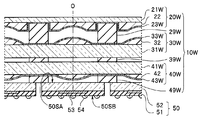
図10に示すように、光学素子ウエハ20W、29W、30W、39W、40W、49Wが接合されることによって、接合ウエハ10Wが作製される。
図10に示すように、光学素子ウエハ20W、29W、30W、39W、40W、49Wが接合されることによって、接合ウエハ10Wが作製される。
例えば、接合面がプラズマ活性化処理された光学素子ウエハ20W、29W、30W、39W、40W、49Wが、室温において圧着接合された後に、120℃1時間の熱処理が行われる。なお、全ての光学素子ウエハを同時に接合する必要はない。
<ステップS30>撮像素子接着工程
図11に示すように、接合ウエハ10Wに複数の撮像部50が接合層(不図示)によって接着される。
図11に示すように、接合ウエハ10Wに複数の撮像部50が接合層(不図示)によって接着される。
撮像部50の作製方法では、半導体ウエハに公知の半導体製造方法によって、CMOS受光素子等の受光部53が受光面50SAに配設される。そして、貫通配線(不図示)を作製することによって、受光部53と裏面50SBの外部接続電極54とが接続された撮像素子ウエハ(不図示)が作製される。撮像素子ウエハの受光面50SAに、ガラスウエハが接着層(不図示)によって接合されてから、切断されることによって、撮像素子51とカバーガラス52とを有する撮像部50が作製される。
なお、光学部10と撮像部50との接合部および撮像素子51とカバーガラス52との接合部も、直接接合されているか、または、有機材料を含まない無機接着剤を用いて接合されている。すなわち、本実施形態の撮像装置では、複数の接合部は、全てが有機材料を含んでいない。
無機接着剤は、透明無機膜と同じ透湿性を有する材料から選択される。例えば、無機接着剤は、水ガラス(シランアルコキシド)等の脱水縮合法(ゾルゲル法)による酸化シリコン層、無機系のバインダを含有する接着剤、融点が100℃~200℃の低融点ガラスまたは半田、からなる。
無機系のバインダとしては、ケイ酸ナトリウム、ケイ酸カリウム、ケイ酸リチウム等のアルカリ金属ケイ酸塩、リン酸アルミニウム、リン酸マグネシウム、リン酸カルシウム等のリン酸塩、またはシリカゾル等を使用できる。
また、無機接着剤は、硬化補助剤として、酸化亜鉛、酸化マグネシウム、酸化カルシウム等の酸化物、水酸化亜鉛、水酸化マグネシウム、水酸化カルシウム等の水酸化物、ホウ酸カルシウム、ホウ酸バリウム、ホウ酸マグネシウム等のホウ酸塩等を含んでいてもよい。
さらに、無機接着剤は、熱収縮によるわれ等の防止のために無機粉体を含んでいてもよい。無機粉体としては、ジルコニア、シリカ、アルミナ、マグネシア、窒化アルミニウム、酸化イットリウム等のセラミックスが例示される。無機粉体は、1種類でもよく、または2種以上を混合して使用してもよい。無機粉体として、アルミナおよびシリカを配合した無機接着剤が好ましい。無機粉体の平均粒径は、0.1μm~5μmの範囲が好ましい。
なお、複数の接合部の少なくともいずれかの接合には、無機接着剤に替えて、透湿性の低い、例えば、透湿度が、30g/(m2×day)以下の有機樹脂からなる接着層を用いてもよい。接着層を経由して水の浸入があったとしても、樹脂レンズの表面は透明無機膜で覆われているので、樹脂レンズそのものは水の影響を受けない。
複数の接合部は、全てが有機材料を含んでいなくともよいし、全てが有機材料を含んでいてもよいし、有機材料を含まない接合部と有機材料を含む接合部とから構成されていてもよい。
<ステップS40>切断工程
図12に示すように、複数の撮像部50が接着された接合ウエハ10Wの切断によって、光学部10と撮像部50とを有する撮像装置1が作製される。ダイシングソー等によって個片化された光学部10の側面10SSには、微細な凹凸である切断痕がある。すなわち、ウエハレベル構造体である光学部10の側面10SSには切断痕がある。また、光学部10を構成している複数の光学素子の外形形状は同一または略同一であり、外寸は同一または略同一(例えば、平均外寸の±5%以内)である。
図12に示すように、複数の撮像部50が接着された接合ウエハ10Wの切断によって、光学部10と撮像部50とを有する撮像装置1が作製される。ダイシングソー等によって個片化された光学部10の側面10SSには、微細な凹凸である切断痕がある。すなわち、ウエハレベル構造体である光学部10の側面10SSには切断痕がある。また、光学部10を構成している複数の光学素子の外形形状は同一または略同一であり、外寸は同一または略同一(例えば、平均外寸の±5%以内)である。
切断工程は、例えば、レーザダイシングによる切断工程、サンドブラストまたはエッチングによる切断溝を形成する個片化工程でもよい。
なお、ガラスウエハに配設される複数の凹レンズは、それぞれが光路面X22を有していれば、外周面Y22が連続していても光学素子としての機能は有している。しかし、外周面Y22が連続している複数の凹レンズは透明無機膜に覆われていても、凹レンズに個片化(切断)されると、側面に凹レンズの樹脂が露出してしまう。
これに対して、撮像装置1ではガラスウエハ21に配設される複数の樹脂レンズ22は、それぞれの樹脂レンズ22の外周面Y22は、隙間(gap)を挾んで分離されているため、それぞれの樹脂レンズ22が外周面Y22を有する。このため、凹レンズに個片化(切断)されると、側面には透明無機膜しか露出しない。
なお、複数の光学素子20等は、全て直方体であり、光軸直交方向の断面が同じ形状かつ同じ大きさのため、光学部10は四角柱である。なお、撮像装置1では、撮像部50の光軸直交方向の断面が、光学部10の光軸直交方向の断面と略同じ形状かつ略同じ大きさである。
すなわち、撮像装置1の小型化のためには、撮像部50の光軸直交方向の断面の大きさが、光学部10の光軸直交方向の断面の大きさ以下であり、光学部10の前面10SAを光軸方向に延長した空間内に、撮像部50が収容されていることが好ましい。
また、接合ウエハ10Wに撮像素子ウエハを接着してから、切断することによって撮像装置1を作製してもよい。この場合には、撮像部50の光軸直交方向の断面が、光学部10の光軸直交方向の断面と同じ形状かつ同じ大きさとなる。
上記製造方法によって、小型であり、かつ耐湿性に優れている撮像装置1を、容易に、かつ、大量に作製することができる。撮像装置1は内視鏡9の硬性先端部90Aに配設される。
<変形例>
次に実施形態の変形例の撮像装置1A~1Dおよび撮像装置1A~1Dを含む変形例の内視鏡9A~9Dについて説明する。変形例の撮像装置1A~1Dまたは変形例の内視鏡9A~9Dは、撮像装置1または内視鏡9と類似し、同じ機能を有しているため、同じ機能の構成要素には同じ符号を付し説明は省略する。
次に実施形態の変形例の撮像装置1A~1Dおよび撮像装置1A~1Dを含む変形例の内視鏡9A~9Dについて説明する。変形例の撮像装置1A~1Dまたは変形例の内視鏡9A~9Dは、撮像装置1または内視鏡9と類似し、同じ機能を有しているため、同じ機能の構成要素には同じ符号を付し説明は省略する。
<変形例1>
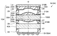
図13に示す撮像装置1Aは、複数の光学素子20A、29、30A、39、40A、49を有する光学部10Aと、撮像部50Aと、を含む。
図13に示す撮像装置1Aは、複数の光学素子20A、29、30A、39、40A、49を有する光学部10Aと、撮像部50Aと、を含む。
光学素子20Aは、凹レンズである樹脂レンズ22Aを有する。樹脂レンズ22Aは外側面Z22が、光軸Oに対して傾斜している。また、スペーサ素子である光学素子29は、光学素子20Aの外周面Y22と接合されている。このため、光学素子20Aの外側面Z22を覆っている透明無機膜23は、光学部10Aの側面10SSに一部が露出している。
光学素子30Aは、ガラス板31の第3の主面31SAに凸レンズである樹脂レンズ32Aは配設され、第4の主面31SBに凸レンズである樹脂レンズ32Bは配設されている。すなわち、ガラス板31の主面の両面に、樹脂レンズ32A、32Bが配設されている。
光学素子40Aは、赤外線を遮断する機能を有する赤外線カットフィルタ素子であり、樹脂レンズは配設されていない。すなわち、光学部10Aは、少なくともいずれかの光学素子が、ハイブリッドレンズ素子であればよい。
撮像部50Aは、撮像素子51であり、カバーガラスを有していない。また、撮像装置1Aの撮像部50Aは、光軸直交方向の断面の大きさが、光学部10Aよりも小さい。
なお、光学素子20A、29、30A、39、40A、49および撮像部50Aは、酸化シリコンからなる接着層によって接着されている。
撮像装置1Aは、樹脂レンズ22A、32A、32Bの表面および樹脂レンズの周囲のガラス板31、32の主面21SB、31SA、31SBが、透明無機膜23、33A、33Bによって覆われている。また、複数の光学素子20A、29、30A、39、40A、49の複数の接合部が、すでに説明した無機接着剤28、37、38、47、48を用いて接合されている。なお、無機接着剤28が、光学素子20Aの外側面Z22を覆っている透明無機膜23を、さらに覆っていることが好ましい。
無機接着剤28、37、38、47、48は、透明無機膜と同じ透湿性を有する材料から選択されるため、撮像装置1Aは、撮像装置1と同じ効果を有する。
なお、複数の接合部の少なくともいずれかが、接着剤を用いることなく、直接接合されており、直接接合されていない接合部が、無機接着剤を用いて接合されていてもよい。
<変形例2>
図14に示すように、変形例2の撮像装置1Bでは、光学素子20Bが、凹レンズおよびスペーサの機能を有している。樹脂からなる光学素子20Bは透明無機膜23によって覆われている。
図14に示すように、変形例2の撮像装置1Bでは、光学素子20Bが、凹レンズおよびスペーサの機能を有している。樹脂からなる光学素子20Bは透明無機膜23によって覆われている。
撮像装置1Bは、撮像装置1Aと比較するとスペーサ素子である光学素子29が不要であるため、構造が簡単であるため製造が容易であるが、撮像装置1Aと同じ効果を有する。すなわち、スペーサ素子は透明無機膜によって覆われている樹脂レンズ素子であってもよい。また、スペーサ素子が透明無機膜によって覆われている樹脂素子であってもよい。
<変形例3、4>
図15に示すように、変形例3の撮像装置1Cでは、光学素子20Cの、ガラス板21の第2の主面21SBに配設されている凹レンズである樹脂レンズ22Cは、外側面Z22の光軸直交方向の形状が、角部が曲線の略矩形である。
図15に示すように、変形例3の撮像装置1Cでは、光学素子20Cの、ガラス板21の第2の主面21SBに配設されている凹レンズである樹脂レンズ22Cは、外側面Z22の光軸直交方向の形状が、角部が曲線の略矩形である。
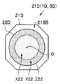
また、図16に示すように、変形例4の撮像装置1Dでは、光学素子20Dの、ガラス板21の第2の主面21SBに配設されている凹レンズである樹脂レンズ22Dは、外側面Z22の光軸直交方向の形状が、円形である。
撮像装置1C、1Dは、外側面Z22の光軸直交方向の形状が直方体である樹脂レンズ22を含む撮像装置1よりも、樹脂レンズ22C、22Dがガラス板21、21Dから剥離しにくい。このため、撮像装置1C、1Dは、撮像装置1よりも、信頼性が高い。
また、撮像装置1Dの光学素子20Dのガラス板21Dは、角部が光軸方向に面取り加工されており、光軸直交方向の断面形状が、六角形である。撮像装置1Dは、光学部の他の光学素子も光学素子20Dと同じく、光軸に平行な角部が面取り加工されている。すなわち、撮像装置1Dの光学部は、四角柱ではなく、六角柱である。
撮像装置1Dは、光軸直交方向のサイズが、撮像装置1よりも小さく、より小型である。
撮像装置1A~1Dを含む内視鏡9A~9Dが、内視鏡9が有する効果に加えて、撮像装置1A~1Dが有する効果を有することは言うまでも無い。
本発明は、上述した実施形態等に限定されるものではなく、発明の趣旨を逸脱しない範囲内において種々の変更、組み合わせおよび応用が可能である。
1、1A~1D・・・内視鏡用撮像装置
8・・・内視鏡システム
9、9A~9D・・・内視鏡
10・・・光学部
10W・・・接合ウエハ
20、29、30、39、40、49・・・光学素子
20W、29W、30W、39W、40W、49W・・・光学素子ウエハ
21、31、41・・・平行平板ガラス板
22、32、42・・・樹脂レンズ
23、33、43・・・透明無機膜
50・・・撮像部
51・・・撮像素子
52・・・カバーガラス
A22・・・接着面
H29・・・貫通孔
X22・・・光路面
Y22・・・外周面
Z22・・・外側面
8・・・内視鏡システム
9、9A~9D・・・内視鏡
10・・・光学部
10W・・・接合ウエハ
20、29、30、39、40、49・・・光学素子
20W、29W、30W、39W、40W、49W・・・光学素子ウエハ
21、31、41・・・平行平板ガラス板
22、32、42・・・樹脂レンズ
23、33、43・・・透明無機膜
50・・・撮像部
51・・・撮像素子
52・・・カバーガラス
A22・・・接着面
H29・・・貫通孔
X22・・・光路面
Y22・・・外周面
Z22・・・外側面
Claims (10)
- 複数の光学素子が接合されており、前記複数の光学素子の少なくともいずれかが、平行平板ガラス板の主面に樹脂レンズが配設されているハイブリッドレンズ素子である光学部と、
前記光学部が集光した被写体像を受光する撮像部と、を具備し、
前記樹脂レンズの表面および前記樹脂レンズの周囲の前記主面が、透明無機膜によって覆われていることを特徴とする内視鏡用撮像装置。 - 前記樹脂レンズが、凹レンズであり、前記透明無機膜によって覆われている前記樹脂レンズの前記表面が、光路面、前記光路面を囲んでいる外周面、および外側面であることを特徴とする請求項1に記載の内視鏡用撮像装置。
- 前記複数の光学素子の複数の接合部の少なくともいずれかが、有機材料を含まないことを特徴とする請求項2に記載の内視鏡用撮像装置。
- 前記複数の接合部の少なくともいずれかが、直接接合されていることを特徴とする請求項3に記載の内視鏡用撮像装置。
- 前記複数の接合部の少なくともいずれかが、無機接着剤を用いて接合されていることを特徴とする請求項3または請求項4に記載の内視鏡用撮像装置。
- 前記複数の光学素子の複数の接合部の少なくともいずれかが、有機接着剤を用いて接合されていることを特徴とする請求項2から請求項5のいずれか1項に記載の内視鏡用撮像装置。
- 前記光学部の側面に切断痕があることを特徴とする請求項2から請求項6のいずれか1項に記載の内視鏡用撮像装置。
- 前記凹レンズの前記外側面の光軸直交方向の形状が、円形または角部が曲線の略矩形であることを特徴とする請求項2から請求項7のいずれか1項に記載の内視鏡用撮像装置。
- 前記複数の光学素子のうちの被写体に最も近い最前部に配置されている第1の光学素子の前面には、前記樹脂レンズが配設されていないことを特徴とする請求項2から請求項8のいずれか1項に記載の内視鏡用撮像装置。
- 請求項1から請求項9のいずれか1項に記載の内視鏡用撮像装置を含むことを特徴とする内視鏡。
Priority Applications (3)
| Application Number | Priority Date | Filing Date | Title |
|---|---|---|---|
| PCT/JP2018/025671 WO2020008618A1 (ja) | 2018-07-06 | 2018-07-06 | 内視鏡用撮像装置、および、内視鏡 |
| CN201880093674.7A CN112189258A (zh) | 2018-07-06 | 2018-07-06 | 内窥镜用摄像装置和内窥镜 |
| US17/123,271 US20210137372A1 (en) | 2018-07-06 | 2020-12-16 | Image pickup apparatus for endoscope and endoscope |
Applications Claiming Priority (1)
| Application Number | Priority Date | Filing Date | Title |
|---|---|---|---|
| PCT/JP2018/025671 WO2020008618A1 (ja) | 2018-07-06 | 2018-07-06 | 内視鏡用撮像装置、および、内視鏡 |
Related Child Applications (1)
| Application Number | Title | Priority Date | Filing Date |
|---|---|---|---|
| US17/123,271 Continuation US20210137372A1 (en) | 2018-07-06 | 2020-12-16 | Image pickup apparatus for endoscope and endoscope |
Publications (1)
| Publication Number | Publication Date |
|---|---|
| WO2020008618A1 true WO2020008618A1 (ja) | 2020-01-09 |
Family
ID=69060045
Family Applications (1)
| Application Number | Title | Priority Date | Filing Date |
|---|---|---|---|
| PCT/JP2018/025671 Ceased WO2020008618A1 (ja) | 2018-07-06 | 2018-07-06 | 内視鏡用撮像装置、および、内視鏡 |
Country Status (3)
| Country | Link |
|---|---|
| US (1) | US20210137372A1 (ja) |
| CN (1) | CN112189258A (ja) |
| WO (1) | WO2020008618A1 (ja) |
Cited By (1)
| Publication number | Priority date | Publication date | Assignee | Title |
|---|---|---|---|---|
| JP2023132925A (ja) * | 2022-03-11 | 2023-09-22 | キヤノン株式会社 | 光学系および撮像装置 |
Families Citing this family (1)
| Publication number | Priority date | Publication date | Assignee | Title |
|---|---|---|---|---|
| WO2023218633A1 (ja) * | 2022-05-13 | 2023-11-16 | オリンパスメディカルシステムズ株式会社 | 撮像ユニット、内視鏡、および、撮像ユニットの製造方法 |
Citations (3)
| Publication number | Priority date | Publication date | Assignee | Title |
|---|---|---|---|---|
| JPH07159601A (ja) * | 1993-12-09 | 1995-06-23 | Hitachi Ltd | 保護膜付き光学素子及びその製造方法並びに電子写真記録装置 |
| JP2011107510A (ja) * | 2009-11-19 | 2011-06-02 | Konica Minolta Opto Inc | 光学素子及び光学素子の製造方法 |
| WO2017203592A1 (ja) * | 2016-05-24 | 2017-11-30 | オリンパス株式会社 | 内視鏡用光学ユニット、内視鏡、および内視鏡用光学ユニットの製造方法 |
Family Cites Families (5)
| Publication number | Priority date | Publication date | Assignee | Title |
|---|---|---|---|---|
| JP4940517B2 (ja) * | 2001-08-07 | 2012-05-30 | ソニー株式会社 | 固体撮像装置およびその製造方法 |
| JP2006119485A (ja) * | 2004-10-25 | 2006-05-11 | Hitachi Maxell Ltd | 光学素子及び光学式記録再生装置 |
| JP4815319B2 (ja) * | 2006-09-29 | 2011-11-16 | 富士フイルム株式会社 | 撮像レンズ及びこれを備えたカメラ装置 |
| TWI530726B (zh) * | 2012-06-15 | 2016-04-21 | 鴻海精密工業股份有限公司 | 鏡片及鏡頭模組 |
| JP2018050769A (ja) * | 2016-09-27 | 2018-04-05 | オリンパス株式会社 | 光学素子、内視鏡用光学ユニット、内視鏡、および内視鏡用光学ユニットの製造方法。 |
-
2018
- 2018-07-06 CN CN201880093674.7A patent/CN112189258A/zh active Pending
- 2018-07-06 WO PCT/JP2018/025671 patent/WO2020008618A1/ja not_active Ceased
-
2020
- 2020-12-16 US US17/123,271 patent/US20210137372A1/en not_active Abandoned
Patent Citations (3)
| Publication number | Priority date | Publication date | Assignee | Title |
|---|---|---|---|---|
| JPH07159601A (ja) * | 1993-12-09 | 1995-06-23 | Hitachi Ltd | 保護膜付き光学素子及びその製造方法並びに電子写真記録装置 |
| JP2011107510A (ja) * | 2009-11-19 | 2011-06-02 | Konica Minolta Opto Inc | 光学素子及び光学素子の製造方法 |
| WO2017203592A1 (ja) * | 2016-05-24 | 2017-11-30 | オリンパス株式会社 | 内視鏡用光学ユニット、内視鏡、および内視鏡用光学ユニットの製造方法 |
Cited By (1)
| Publication number | Priority date | Publication date | Assignee | Title |
|---|---|---|---|---|
| JP2023132925A (ja) * | 2022-03-11 | 2023-09-22 | キヤノン株式会社 | 光学系および撮像装置 |
Also Published As
| Publication number | Publication date |
|---|---|
| CN112189258A (zh) | 2021-01-05 |
| US20210137372A1 (en) | 2021-05-13 |
Similar Documents
| Publication | Publication Date | Title |
|---|---|---|
| US12015045B2 (en) | Manufacturing method of image pickup apparatus for endoscope, image pickup apparatus for endoscope, and endoscope | |
| US20190079280A1 (en) | Manufacturing method of optical unit for endoscope, optical unit for endoscope, and endoscope | |
| WO2017203594A1 (ja) | 内視鏡用撮像ユニット、および内視鏡 | |
| WO2016147556A1 (ja) | 光コネクタ、光コネクタセット、撮像ユニット、撮像システム及び光伝送モジュール | |
| US11096567B2 (en) | Endoscope system and method of manufacturing an image capturing module used in the endoscope system | |
| WO2018198266A1 (ja) | 内視鏡、撮像モジュール、および、撮像モジュールの製造方法 | |
| JP2013013712A (ja) | 電子内視鏡装置及びその製造方法 | |
| WO2020008618A1 (ja) | 内視鏡用撮像装置、および、内視鏡 | |
| WO2022234627A1 (ja) | 撮像ユニット、および、内視鏡 | |
| JP2002050751A (ja) | 固体撮像素子用カバーガラス | |
| JP5074133B2 (ja) | 撮像装置用プリズムユニット | |
| WO2020084728A1 (ja) | 内視鏡レンズユニット、内視鏡、および、内視鏡レンズユニットの製造方法 | |
| CN109952646B (zh) | 摄像模块以及内窥镜 | |
| US20210099620A1 (en) | Image pickup apparatus, endoscope, and manufacturing method of image pickup apparatus | |
| WO2011092904A1 (ja) | 内視鏡先端部構造 | |
| TW201325540A (zh) | 整合光源的內視鏡 | |
| JP7627764B2 (ja) | 撮像装置、および、内視鏡 | |
| CN112136213B (zh) | 摄像装置、内窥镜和摄像装置的制造方法 | |
| WO2023002540A1 (ja) | レンズユニット、撮像装置、および、内視鏡 | |
| WO2023218633A1 (ja) | 撮像ユニット、内視鏡、および、撮像ユニットの製造方法 | |
| WO2023007652A1 (ja) | レンズユニット、撮像装置、内視鏡、および、レンズユニットの製造方法 | |
| WO2019138463A1 (ja) | 光学ユニットの製造方法、光学ユニット、および内視鏡 | |
| WO2019171460A1 (ja) | 内視鏡用撮像装置、内視鏡、および内視鏡用撮像装置の製造方法 | |
| US12564308B2 (en) | Image pickup unit, endoscope, and method for manufacturing image pickup unit | |
| WO2021176704A1 (ja) | 光学ユニット、光学ユニットの製造方法、および、内視鏡 |
Legal Events
| Date | Code | Title | Description |
|---|---|---|---|
| 121 | Ep: the epo has been informed by wipo that ep was designated in this application |
Ref document number: 18925379 Country of ref document: EP Kind code of ref document: A1 |
|
| NENP | Non-entry into the national phase |
Ref country code: DE |
|
| 122 | Ep: pct application non-entry in european phase |
Ref document number: 18925379 Country of ref document: EP Kind code of ref document: A1 |
|
| NENP | Non-entry into the national phase |
Ref country code: JP |