WO2020008569A1 - 第1コネクタ、第2コネクタ、および、コネクタ装置 - Google Patents
第1コネクタ、第2コネクタ、および、コネクタ装置 Download PDFInfo
- Publication number
- WO2020008569A1 WO2020008569A1 PCT/JP2018/025375 JP2018025375W WO2020008569A1 WO 2020008569 A1 WO2020008569 A1 WO 2020008569A1 JP 2018025375 W JP2018025375 W JP 2018025375W WO 2020008569 A1 WO2020008569 A1 WO 2020008569A1
- Authority
- WO
- WIPO (PCT)
- Prior art keywords
- connector
- signal terminal
- terminal
- frame
- ground
- Prior art date
- Legal status (The legal status is an assumption and is not a legal conclusion. Google has not performed a legal analysis and makes no representation as to the accuracy of the status listed.)
- Ceased
Links
Images








Classifications
-
- H—ELECTRICITY
- H01—ELECTRIC ELEMENTS
- H01R—ELECTRICALLY-CONDUCTIVE CONNECTIONS; STRUCTURAL ASSOCIATIONS OF A PLURALITY OF MUTUALLY-INSULATED ELECTRICAL CONNECTING ELEMENTS; COUPLING DEVICES; CURRENT COLLECTORS
- H01R13/00—Details of coupling devices of the kinds covered by groups H01R12/70 or H01R24/00 - H01R33/00
- H01R13/648—Protective earth or shield arrangements on coupling devices, e.g. anti-static shielding
- H01R13/6485—Electrostatic discharge protection
-
- H—ELECTRICITY
- H01—ELECTRIC ELEMENTS
- H01R—ELECTRICALLY-CONDUCTIVE CONNECTIONS; STRUCTURAL ASSOCIATIONS OF A PLURALITY OF MUTUALLY-INSULATED ELECTRICAL CONNECTING ELEMENTS; COUPLING DEVICES; CURRENT COLLECTORS
- H01R13/00—Details of coupling devices of the kinds covered by groups H01R12/70 or H01R24/00 - H01R33/00
- H01R13/648—Protective earth or shield arrangements on coupling devices, e.g. anti-static shielding
- H01R13/652—Protective earth or shield arrangements on coupling devices, e.g. anti-static shielding with earth pin, blade or socket
-
- H—ELECTRICITY
- H01—ELECTRIC ELEMENTS
- H01R—ELECTRICALLY-CONDUCTIVE CONNECTIONS; STRUCTURAL ASSOCIATIONS OF A PLURALITY OF MUTUALLY-INSULATED ELECTRICAL CONNECTING ELEMENTS; COUPLING DEVICES; CURRENT COLLECTORS
- H01R2107/00—Four or more poles
-
- H—ELECTRICITY
- H01—ELECTRIC ELEMENTS
- H01R—ELECTRICALLY-CONDUCTIVE CONNECTIONS; STRUCTURAL ASSOCIATIONS OF A PLURALITY OF MUTUALLY-INSULATED ELECTRICAL CONNECTING ELEMENTS; COUPLING DEVICES; CURRENT COLLECTORS
- H01R24/00—Two-part coupling devices, or either of their cooperating parts, characterised by their overall structure
- H01R24/60—Contacts spaced along planar side wall transverse to longitudinal axis of engagement
- H01R24/62—Sliding engagements with one side only, e.g. modular jack coupling devices
Definitions
- the present invention relates to a first connector, a second connector, and a connector device.
- the receptacle described in Patent Document 1 is defined by an interface standard for performing data transfer using differential signals.
- the receptacle transmits a signal by being connected to the plug.
- the receptacle includes a power terminal, a ground terminal, a first differential signal terminal transmitting a first differential signal, a second differential signal terminal transmitting a second differential signal, and a protection element.
- the protection element is provided between the power supply terminal and the ground terminal.
- the protection element protects the electronic device on which the receptacle is mounted from a transient voltage or static electricity that enters the power supply terminal or the ground terminal of the receptacle from the outside.
- the protection element includes a chip capacitor and a Zener diode. Zener diodes can be replaced with varistors.
- the receptacle described in Patent Document 1 requires electronic components such as a chip capacitor and a zener diode. Therefore, in order to protect the electronic device on which the receptacle is mounted from electrostatic discharge (Electrostatic Discharge: EDS), the manufacturing cost of the receptacle (a type of connector) increases.
- EDS Electrostatic Discharge
- An object of the present invention is to provide a first connector, a second connector, and a connector device that can reduce manufacturing costs while protecting electronic devices from electrostatic discharge.
- the first connector is connected to the second connector.
- the first connector includes a first frame, a first signal terminal, and a ground unit.
- the first frame has a first opening.
- the second connector is inserted into the first frame through the first opening.
- the first signal terminal is arranged inside the first frame, and is connected to a second signal terminal of the second connector. After the insertion of the second connector into the first frame body is started, the grounding portion is in a connected state in which the insertion is completed and the first signal terminal and the second signal terminal are connected.
- the second signal terminal is disposed so as to contact the second signal terminal before and separate from the second signal terminal in the connection state.
- the second connector is connected to the first connector.
- the second connector includes the second signal terminal.
- the second signal terminal is in contact with the ground portion before the connection state is established after the insertion of the second connector into the first frame is started, and is separated from the ground portion in the connection state. are doing.
- a connector device includes the first connector and the second connector.
- manufacturing costs can be reduced while protecting electronic devices from electrostatic discharge.
- FIG. 2 is a perspective view illustrating a first connector of the connector device according to the first embodiment of the present invention.
- FIG. 2 is a plan view illustrating a first connector of the connector device according to the first embodiment.
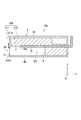
- FIG. 3 is a cross-sectional view illustrating a first connector of the connector device according to the first embodiment.
- FIG. 3 is a perspective view illustrating a second connector of the connector device according to the first embodiment.
- FIG. 3 is a plan view illustrating a second connector of the connector device according to the first embodiment.
- FIG. 3 is a cross-sectional view illustrating a second connector of the connector device according to the first embodiment.
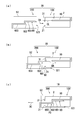
- FIG. 2A is a schematic cross-sectional view illustrating a state where a first connector and a second connector of the connector device according to the first embodiment are separated from each other.
- FIG. 3B is a schematic cross-sectional view illustrating a state where the first connector and the second connector of the connector device according to the first embodiment are being connected.
- FIG. 3C is a schematic cross-sectional view illustrating a connection state in which the first connector and the second connector of the connector device according to the first embodiment are connected.
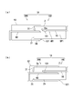
- FIG. 2A is a schematic plan view illustrating a state where a first connector and a second connector of the connector device according to the first embodiment are separated from each other.
- FIG. 2B is a schematic plan view illustrating a state where the first connector and the second connector of the connector device according to the first embodiment are being connected.
- FIG. 3C is a schematic plan view illustrating a connection state in which the first connector and the second connector of the connector device according to the first embodiment are connected.
- FIG. 7A is a schematic cross-sectional view illustrating a state where the first connector and the second connector of the connector device according to the first modification of the first embodiment are being connected.
- FIG. 4B is a schematic cross-sectional view illustrating a connection state in which the first connector and the second connector of the connector device according to the first modification of the first embodiment are connected.
- FIG. 10 is a cross-sectional view illustrating a first connector of the connector device according to the second embodiment.
- A is a typical sectional view showing the state where the 1st connector and the 2nd connector of the connector device concerning Embodiment 2 were separated.
- 9B is a schematic cross-sectional view illustrating a state where the first connector and the second connector of the connector device according to the second embodiment are being connected.
- C is a schematic sectional view showing a connected state where the first connector and the second connector of the connector device according to Embodiment 2 are connected.
- A is a typical sectional view showing the state where the 1st connector and the 2nd connector of the connector device concerning the 1st modification of Embodiment 2 are connected.
- (B) is a schematic sectional view showing the connected state where the 1st connector and the 2nd connector of the connector device concerning the 1st modification of Embodiment 2 are connected.
- (A) is a typical sectional view showing the state where the 1st connector and the 2nd connector of the connector device concerning the 2nd modification of Embodiment 2 are connected.
- (B) is a schematic sectional view showing the connected state where the first connector and the second connector of the connector device according to the second modified example of the second embodiment are connected. It is sectional drawing which shows the 1st connector of the connector apparatus which concerns on the 3rd modification of Embodiment 2.
- connection device 1 The connector device according to the first embodiment of the present invention (hereinafter, referred to as “connector device 1”) will be described with reference to FIGS. 1 to 8C.
- the connector device 1 realizes electrical connection.
- the connector device 1 will be described with reference to FIGS.
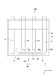
- FIG. 1 is a perspective view showing the first connector 100 of the connector device 1.
- FIG. 2 is a plan view showing the first connector 100.
- FIG. In FIG. 2, the first connector 100 is viewed from the direction D1 of FIG.
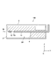
- FIG. 3 is a sectional view showing the first connector 100.
- FIG. 3 shows a cross section when the first connector 100 is viewed from the direction D2 in FIG.
- FIG. 4 is a perspective view showing the second connector 200 of the connector device 1.
- FIG. 5 is a plan view showing the second connector 200.
- FIG. 5 is viewed from the direction D3 in FIG.
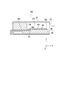
- FIG. 6 is a sectional view showing the second connector 200.
- FIG. 6 shows a cross section when the second connector 200 is viewed from the direction D4 in FIG.
- the connector device 1 includes a first connector 100 and a second connector 200.
- the first connector 100 is electrically connected to the second connector 200.
- the second connector 200 is electrically connected to the first connector 100. Therefore, each of the first connector 100 and the second connector 200 is an electrical connector.
- the second connector 200 is moved in the first direction DA and fitted to the first connector 100. Then, the second connector 200 is electrically connected to the first connector 100.
- the first direction DA corresponds to the “insertion direction of the second connector 200”.
- the first connector 100 includes a first frame 2, a first holder 4, a first power supply terminal 6, a first ground terminal 8, and a plurality of first signal terminals. 10 and a grounding unit 12.
- the first connector 100 includes two first signal terminals 10.
- the first connector 100 is a type A receptacle conforming to the USB (Universal Serial Bus) standard.
- the first frame 2 is indicated by a dashed line
- the first holder 4 is indicated by a two-dot chain line for easy viewing of the drawings.
- the first frame 2 is hollow and has a substantially rectangular parallelepiped shape.
- the first frame 2 is, for example, in a substantially rectangular tube shape.
- the material of the first frame 2 is a conductive material.
- the first frame 2 is made of, for example, metal.
- the first frame 2 is grounded, for example.
- the first frame 2 has a substantially rectangular first opening 21.
- the second connector 200 is inserted into the first frame 2 through the first opening 21. Specifically, when the second connector 200 is connected to the first connector 100, the second connector 200 passes through the first opening 21 in the first direction DA.
- the first direction DA is substantially orthogonal to the first opening 21.
- the side where the first opening 21 is located is the front or front side of the first connector 100, and the side opposite to the first opening 21 is the rear or rear side of the first connector 100.
- the rear end of the first frame 2 is covered with a cover (not shown) made of synthetic resin.
- the first holding member 4 has a one-step shape. That is, the first holding body 4 has a shape in which two substantially rectangular parallelepiped flat plates are joined while being shifted in the first direction DA.
- the material of the first holder 4 is an electrically insulating material.
- the first holder 4 is made of, for example, a synthetic resin.
- the first holder 4 is arranged inside the first frame 2.
- each of the first power supply terminal 6, the plurality of first signal terminals 10, and the first ground terminal 8 is a conductive material.
- Each of the first power supply terminal 6, the plurality of first signal terminals 10, and the first ground terminal 8 is made of, for example, metal.
- the first power terminal 6, the plurality of first signal terminals 10, and the first ground terminal 8 are arranged inside the first frame 2.
- the first power supply terminal 6, the plurality of first signal terminals 10, and the first ground terminal 8 are arranged substantially parallel to each other with an interval therebetween.
- the plurality of first signal terminals 10 are arranged between the first power terminal 6 and the first ground terminal 8.
- the first power supply terminal 6, the plurality of first signal terminals 10, and the first ground terminal 8 are held by the first holder 4. Then, as shown in FIGS. 2 and 3, a part of each of the first power supply terminal 6, the plurality of first signal terminals 10, and the first ground terminal 8 is connected to the inner space SP ⁇ b> 1 of the first frame 2. 1 is exposed from the holder 4. A part of each of the first power supply terminal 6, the plurality of first signal terminals 10, and the first ground terminal 8 is located on the first opening 21 side.
- FIG. 3 shows a cross section when the first signal terminal 10 and the ground portion 12 are cut along a cutting plane parallel to the YZ plane.
- Each of the first power supply terminal 6, the plurality of first signal terminals 10, and the first ground terminal 8 extends in the direction away from the first opening 21 from the first opening 21 inside the first frame 2. I have. In other words, each of the first power supply terminal 6, the plurality of first signal terminals 10, and the first ground terminal 8 extends in the first direction DA from the side of the first opening 21 inside the first frame 2. ing. In other words, each of the first power supply terminal 6, the plurality of first signal terminals 10, and the first ground terminal 8 extends along the first direction DA inside the first frame 2. In this specification, “along the first direction DA” means “substantially parallel to the first direction DA”.
- a power supply voltage is applied to the first power supply terminal 6.
- the first ground terminal 8 is grounded.
- the first ground terminal 8 has a ground potential.
- a signal voltage is applied to each of the first signal terminals 10.
- one signal voltage (D +) of two signal voltages forming a differential signal is applied to one of the two first signal terminals 10, and the other signal signal is applied to the other first signal terminal 10.
- the other signal voltage (D ⁇ ) is applied to the first signal terminal 10.
- the first ground terminal 8 includes the end 8a.
- the end 8 a is an end on the first opening 21 side of both ends of the first ground terminal 8.
- the first signal terminal 10 includes an end 10a.
- the end 10 a is an end on the first opening 21 side of both ends of the first signal terminal 10.
- the grounding section 12 is grounded. When the grounding section 12 is grounded, the grounding section 12 has a ground potential.
- the grounding portion 12 is a flat, substantially plate-shaped member.
- the material of the ground part 12 is a conductive material.
- the grounding part 12 is made of, for example, metal.
- the ground portion 12 extends from the end 8 a of the first ground terminal 8 so as to pass between the end 10 a of the first signal terminal 10 and the first opening 21.
- the grounding section 12 extends the first signal terminal 10 from the end 10 a on the first opening 21 side of the first signal terminal 10 toward the first opening 21 along the first direction DA. It is located on the area.
- the “extended area” for the first signal terminal 10 is referred to as “extended area EA”.
- the grounding section 12 is disposed so as to intersect with each extension line EL of the first signal terminal 10.
- the extension line EL extends along the first direction DA from the end 10 a of the first signal terminal 10 on the first opening 21 side toward the first opening 21.
- the extension line EL is a line within the extension area EA.
- the ground portion 12 bends from the end 8 a of the first ground terminal 8 and extends so as to pass between the end 10 a of the first signal terminal 10 and the first opening 21. More specifically, the grounding portion 12 is bent at a substantially right angle from the end 8 a of the first ground terminal 8 and extends so as to pass between the end 10 a of the first signal terminal 10 and the first opening 21. Therefore, the ground portion 12 extends along the direction DB.
- the grounding section 12 is disposed between the first opening 21 and the end 10a of the first signal terminal 10.
- the direction DB is substantially orthogonal to the first direction DA and indicates a direction from the first ground terminal 8 to the first power supply terminal 6. Note that the first power supply terminal 6, the plurality of first signal terminals 10, and the first ground terminal 8 are arranged along the direction DB.
- the grounding unit 12 is configured as a part of the first grounding terminal 8. That is, the ground portion 12 and the first ground terminal 8 are integrally molded products. Therefore, the number of parts of the first connector 100 can be reduced. As a result, the manufacturing cost of the first connector 100 can be reduced. As shown in FIG. 2, the integrally molded product including the ground portion 12 and the first ground terminal 8 is substantially L-shaped in plan view.
- the first ground terminal 8 has a first portion 81 and a second portion 82.
- the first portion 81 extends along the first direction DA.
- the second portion 82 extends from the end 8 a of the first portion 81 on the first opening 21 side so as to pass between the first signal terminal 10 and the first opening 21. Then, the second portion 82 of the first grounding terminal 8 forms the grounding portion 12.
- the second connector 200 includes a second frame 52, a second holder 54, a second power supply terminal 56, a second ground terminal 58, and a plurality of second signal terminals. 60.
- the plurality of second signal terminals 60 are provided corresponding to the plurality of first signal terminals 10 of the first connector 100. Each of the plurality of second signal terminals 60 is connected to the corresponding first signal terminal 10.
- the second connector 200 includes two second signal terminals 60 corresponding to the two first signal terminals 10, respectively.
- the second connector 200 is a type A plug conforming to the USB standard.
- the second frame 52 is indicated by a dashed line and the second holder 54 is indicated by a two-dot chain line for easy viewing of the drawings.
- the second frame 52 is hollow and has a substantially rectangular parallelepiped shape.
- the second frame 52 is, for example, in a substantially rectangular tube shape.
- the material of the second frame 52 is a conductive material.
- the second frame 52 is made of, for example, metal.
- the second frame 52 is grounded, for example.
- the second frame 52 has a substantially rectangular second opening 521.
- the side where the second opening 521 is located is the front or front side of the second connector 200, and the side opposite to the second opening 521 is the rear or rear side of the second connector 200.
- the rear end of the second frame 52 is covered with a cover (not shown) made of synthetic resin.
- the second holding member 54 has a one-step shape. That is, the second holding member 54 has a shape in which two substantially rectangular parallelepiped flat plates are shifted in the first direction DA and joined.
- the material of the second holder 54 is an electrically insulating material.
- the second holder 54 is made of, for example, a synthetic resin.
- the second holder 54 is arranged inside the second frame 52.
- each of the second power supply terminal 56, the plurality of second signal terminals 60, and the second ground terminal 58 is a conductive material.
- Each of the second power supply terminal 56, the plurality of second signal terminals 60, and the second ground terminal 58 is made of, for example, metal.
- the second power terminal 56, the plurality of second signal terminals 60, and the second ground terminal 58 are disposed inside the second frame 52.
- the second power supply terminal 56, the plurality of second signal terminals 60, and the second ground terminal 58 are arranged substantially in parallel at intervals.
- the plurality of second signal terminals 60 are arranged between the second power terminal 56 and the second ground terminal 58.
- the second power supply terminal 56, the plurality of second signal terminals 60, and the second ground terminal 58 are held by the second holder 54. Then, as shown in FIGS. 5 and 6, a part of each of the second power supply terminal 56, the plurality of second signal terminals 60, and the second ground terminal 58 is connected to the inner space SP ⁇ b> 2 of the second frame 52. 2 is exposed from the holder 54. A part of each of the second power supply terminal 56, the plurality of second signal terminals 60, and the second ground terminal 58 is located on the side of the second opening 521.
- FIG. 6 shows a cross section when the second signal terminal 60 is cut along a cutting plane parallel to the YZ plane.
- Each of the second power supply terminal 56, the plurality of second signal terminals 60, and the second ground terminal 58 extends from the second opening 521 side in the direction away from the second opening 521 inside the second frame 52. I have. In other words, each of the second power supply terminal 56, the plurality of second signal terminals 60, and the second ground terminal 58 is located inside the second frame 52 from the side of the second opening 521 in the first direction DA. And extends in the opposite second direction DC. In other words, each of the second power supply terminal 56, the plurality of second signal terminals 60, and the second ground terminal 58 extends along the first direction DA inside the second frame 52.
- the second power supply terminal 56 is bent at a predetermined position P ⁇ b> 1 into the second holding body 54 inside the second frame 52, and extends in a direction away from the second opening 521.
- the second power supply terminal 56 includes an end 56a.
- the end portion 56a is an end portion on the side of the second opening 521 among both end portions of the second power supply terminal 56.
- the end 56a is inclined at an acute angle with respect to the first direction DA.
- the predetermined position P1 indicates a position farther from the second opening 521 than the end portion 56a of the second power supply terminal 56.
- a power supply voltage is applied to the second power supply terminal 56.
- the second grounding terminal 58 is bent at a predetermined position P2 inside the second frame body 52, enters the second holding body 54, and extends in a direction away from the second opening 521.
- the second ground terminal 58 includes an end 58a.
- the end 58a is an end on the side of the second opening 521 among both ends of the second ground terminal 58.
- the end 58a is inclined at an acute angle with respect to the first direction DA.
- the predetermined position P2 indicates a position farther from the second opening 521 than the end 58a of the second ground terminal 58.
- the second ground terminal 58 is grounded. When the second ground terminal 58 is grounded, the second ground terminal 58 has a ground potential.
- the second signal terminal 60 is bent inside the second frame 52 at a predetermined position P ⁇ b> 3, enters the second holding member 54, and extends away from the second opening 521. That is, the second signal terminal 60 bends at the predetermined position P ⁇ b> 3 inside the second frame 52, enters the second holder 54, and extends in the second direction DC.
- the second signal terminal 60 includes an end 60a.
- the end 60 a is an end on the second opening 521 side of both ends of the second signal terminal 60.
- the end 60a is inclined at an acute angle with respect to the first direction DA.
- the predetermined position P3 indicates a position farther from the second opening 521 than the end 60a of the second signal terminal 60.
- the second signal terminal 60 has a substantially linear contact portion 601, a bent portion 602, and a substantially linear non-contact portion 603.
- the contact portion 601 is exposed in the internal space SP2 of the second frame 52.
- connection state CS indicates a state in which the first connector 100 and the second connector 200 are fitted with each other, and the first connector 100 and the second connector 200 are completely connected. Therefore, the connection state CS does not include a state during connection even when the first connector 100 and the second connector 200 are in contact with each other.
- the non-contact portion 603 is separated from the first signal terminal 10 (FIG. 3) of the first connector 100 in the connection state CS and does not contact the first signal terminal 10.
- the bent portion 602 is bent at a predetermined position P3, and connects the contact portion 601 and the non-contact portion 603.
- a signal voltage is applied to each of the second signal terminals 60.
- one signal voltage (D +) of two signal voltages constituting a differential signal is applied to one second signal terminal 60 of the two second signal terminals 60, and the other signal voltage is applied to the other signal signal.
- the other signal voltage (D ⁇ ) is applied to the second signal terminal 60.
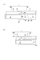
- FIGS. 7A and 8A are a schematic cross-sectional view and a plan view, respectively, showing a state where the first connector 100 and the second connector 200 are separated from each other.
- FIGS. 7B and 8B are a schematic cross-sectional view and a plan view, respectively, showing a state in which the first connector 100 and the second connector 200 are being connected.
- FIGS. 7C and 8C are a schematic cross-sectional view and a plan view showing a connection state CS in which the first connector 100 and the second connector 200 are connected. Note that, in FIGS.
- the first holder 4 and the second holder 54 are omitted for easy viewing of the drawings.
- the second connector 200 is indicated by a thick line in order to clearly distinguish the first connector 100 from the second connector 200.
- the first connector 100 and the second connector 200 are separated. Then, the second connector 200 is moved in the first direction DA toward the first connector 100.
- the second signal terminal 60 of the second connector 200 passes through the first opening 21 of the first connector 100.
- the ground portion 12 of the first connector 100 is arranged on the first opening 21 side with respect to the first signal terminal 10. Therefore, before the first signal terminal 10 contacts the second signal terminal 60, the grounding portion 12 contacts the second signal terminal 60.
- the insertion is completed and the first signal terminal 10 and the second signal terminal 60 are connected.
- the grounding section 12 contacts the second signal terminal 60.
- the second signal terminal 60 contacts the ground portion 12 after the insertion of the second connector 200 into the first frame 2 is started and before the connection state is established.
- the first signal terminal 10 may be caused by the static electricity of the second signal terminal 60 before the first signal terminal 10 contacts the second signal terminal 60.
- the discharged charge can be discharged through the grounding section 12.
- the electronic device on which the first connector 100 is mounted can be protected from electrostatic discharge (ESD).
- Electrostatic discharge is a phenomenon in which electrostatic discharge occurs when charged objects come into contact with each other. Note that the connection state in which the first signal terminal 10 and the second signal terminal 60 are connected substantially indicates the connection state CS. Therefore, the connection state in which the first signal terminal 10 and the second signal terminal 60 are connected is also described as “connection state CS”.
- the first connector 100 includes the grounding portion 12 as a component for protecting the electronic device from electrostatic discharge. Therefore, the first connector 100 and the second connector 200 are not required to include electronic components (such as a chip capacitor, a zener diode, and a varistor) for preventing electrostatic discharge. Further, there is no need to perform an operation of electrically connecting electronic components for measures against electrostatic discharge. As a result, the manufacturing cost of the first connector 100 and the second connector 200 can be reduced. In other words, the manufacturing cost of the connector device 1 can be reduced.
- the first connector 100 is mounted on the first connector 100 while protecting the electronic device from the electrostatic discharge.
- 100 and the manufacturing cost of the second connector 200 can be reduced.
- the manufacturing cost of the connector device 1 can be reduced while protecting the electronic device on which the first connector 100 is mounted from electrostatic discharge.
- the countermeasure against electrostatic discharge can be easily performed by the grounding portion 12.
- the end 60a of the second signal terminal 60 is inclined. Therefore, the second signal terminal 60 (specifically, the end portion 60a) can travel in the first direction DA while smoothly abutting on the ground portion 12.
- the grounding portion 12 extends between the end 8 a of the first ground terminal 8 and the end 10 a of the first signal terminal 10 and the first opening 21. Extend to pass through. Therefore, as shown in FIG. 8B, the second signal terminal 60 easily contacts the ground portion 12 before contacting the first signal terminal 10. As a result, the charge caused by the static electricity of the second signal terminal 60 can be easily discharged through the grounding portion 12, and the electronic device on which the first connector 100 is mounted can be protected from the electrostatic discharge.
- the grounding portion 12 is disposed on the extension area EA with respect to the first signal terminal 10 (in the first embodiment, on the extension line EL) (FIGS.
- the first signal terminal 10 is not connected to the first signal terminal 10.
- the second signal terminal 60 Before contacting the second signal terminal 60, the second signal terminal 60 can be more easily brought into contact with the grounding portion 12. As a result, the charge caused by the static electricity of the second signal terminal 60 can be more easily discharged through the grounding portion 12.
- the grounding portion 12 crosses the second signal terminal 60.
- the grounding section 12 is substantially orthogonal to the second signal terminal 60.
- second power terminal 56 contacts first power terminal 6 and second ground terminal 58 contacts the first ground terminal 8.
- the second power terminal 56 may not be in contact with the first power terminal 6, and the second ground terminal 58 is in contact with the first ground terminal 8. It is not necessary.
- connection state CS the second power terminal 56 is in contact with the first power terminal 6, and the second ground terminal 58 is in contact with the first ground terminal 8.
- first power terminal 6 is connected to the second power terminal 56
- first ground terminal 8 is connected to the second ground terminal 58.
- the grounding part 12 is arranged so as to be separated from the second signal terminal 60 in the connection state CS in which the first signal terminal 10 and the second signal terminal 60 are connected.
- the second signal terminal 60 is separated from the ground part 12 in the connection state CS.
- the signal voltage can be transmitted from the first signal terminal 10 to the second signal terminal 60, Alternatively, a signal voltage can be transmitted from the second signal terminal 60 to the first signal terminal 10.
- the first signal terminal 10 and the second signal terminal 60 are in contact with each other due to the elasticity of the first signal terminal 10 and the second signal terminal 60. Due to the elasticity of the first power terminal 6 and the second power terminal 56, the first power terminal 6 and the second power terminal 56 come into contact with each other. Due to the elasticity of the first ground terminal 8 and the second ground terminal 58, the first ground terminal 8 and the second ground terminal 58 come into contact with each other.
- the second signal terminal 60 Bent away. Therefore, in the connection state CS, the ground portion 12 and the second signal terminal 60 can be easily separated from each other by a simple structure. As a result, transmission of the signal voltage between the first signal terminal 10 and the second signal terminal 60 can be prevented from being hindered by the grounding portion 12.
- the non-contact portion 603 of the second signal terminal 60 extends in the second direction DC while being separated from the ground portion 12. Therefore, the non-contact part 603 is separated from the ground part 12 and the first signal terminal 10. In particular, since the non-contact portion 603 is covered by the second holder 54 (FIG. 6), it does not contact the ground portion 12.
- the contact portion 601 is in contact with the first signal terminal 10 while being separated from the ground portion 12. Note that the first opening 21 of the first frame 2 is larger than the outer periphery of the second opening 521 of the second frame 52. Therefore, the second connector 200 is fitted inside the first connector 100.
- FIGS. 9A to 10B 9 (a) to 10 (b), the first holder 4 and the second holder 54 are omitted for easy viewing of the drawings.
- a connector device 1 according to a first modification of the first embodiment will be described with reference to FIGS. 9A and 9B.
- the first modification is the connector device 1 according to the first modification in that the ground portion 12 and the second signal terminal 60 are separated by the first protrusion 101 of the first signal terminal 10 in the connection state CS. This is mainly different from the first embodiment described with reference to FIG.
- the points in which the first modified example is different from the first embodiment will be mainly described.
- FIG. 9A is a schematic cross-sectional view showing a state where the first connector 100 and the second connector 200 according to the first modification are being connected.
- FIG. 9B is a schematic cross-sectional view illustrating a connection state CS in which the first connector 100 and the second connector 200 according to the first modification are connected.
- each of the first signal terminals 10 includes a first convex portion 101.
- the first protrusion 101 projects into the internal space SP1 of the first frame 2.
- the first convex portion 101 protrudes into the entry area AR1 of the second signal terminal 60 in the internal space SP1 of the first frame 2.
- the first convex portion 101 is arranged near the end 10a of the first signal terminal 10 in the first modification.
- the first convex portion 101 is disposed in the front region of the front region and the rear region of the first signal terminal 10.
- the first convex portion 101 has, for example, a substantially semicircular shape, a substantially circular arc shape, or a substantially polygonal shape (for example, a substantially triangular shape) in a sectional view.
- the first convex portion 101 has, for example, a curved surface. Therefore, the second signal terminal 60 (specifically, the end portion 60a) can travel in the first direction DA while smoothly abutting on the first convex portion 101.
- the second signal terminal 60 contacts the ground portion 12 before contacting the first signal terminal 10. Therefore, even when the second signal terminal 60 has static electricity, before the first signal terminal 10 comes into contact with the second signal terminal 60, the charge caused by the static electricity of the second signal terminal 60 is transferred to the ground portion 12. Can be discharged through.
- connection state CS the state of the connector device 1 becomes the connection state CS.
- the connection state CS the first protrusion 101 is in contact with the second signal terminal 60.
- the elasticity of the first signal terminal 10 and the second signal terminal 60 causes the first convex portion 101 and the second signal terminal 60 to be in contact with each other. That is, the first convex portion 101 contacts the second signal terminal 60.
- the first protrusion 101 separates the second signal terminal 60 from the grounding portion 12. Therefore, according to the first modification, even in the case where the first connector 100 includes the grounding portion 12, the signal voltage can be transmitted from the first signal terminal 10 to the second signal terminal 60 in the connection state CS. Alternatively, a signal voltage can be transmitted from the second signal terminal 60 to the first signal terminal 10.
- the second signal terminal 60 is separated from the ground portion 12 by the first convex portion 101 in the connection state CS. It is not necessary to have the contact part 603 (FIG. 6). Therefore, in the first modified example, the second signal terminal 60 can be separated from the ground portion 12 with a simple configuration like the first convex portion 101.
- a connector device 1 according to a second modification of the first embodiment will be described with reference to FIGS. 10A and 10B.
- the second modification is different from the connector device 1 according to the second modification in that the ground portion 12 and the second signal terminal 60 are separated by the second protrusion 605 of the second signal terminal 60 in the connection state CS.
- This is mainly different from the first embodiment described with reference to FIG.
- the points in which the second modified example is different from the first embodiment will be mainly described.
- FIG. 10A is a schematic cross-sectional view showing a state where the first connector 100 and the second connector 200 according to the second modification are being connected.
- FIG. 10B is a schematic cross-sectional view illustrating a connection state CS in which the first connector 100 and the second connector 200 according to the second modification are connected.
- each of the second signal terminals 60 includes a plurality of second convex portions 605.
- each of the second signal terminals 60 includes two second convex portions 605.
- the second protrusion 605 closer to the second opening 521 is referred to as a second protrusion 605a
- the second protrusion 605 farther from the second opening 521 is referred to as a second protrusion. It may be described as a part 605b.
- each of the second protrusions 605 protrudes into the internal space SP2 of the second frame 52. Specifically, each of the second protrusions 605 protrudes into the entry area AR2 of the first signal terminal 10 in the internal space SP1 of the second frame 52.
- the second convex portion 605a is arranged near the end 60a of the second signal terminal 60 in the second modification. Specifically, the second convex portion 605a is disposed in the front region of the front region and the rear region of the second signal terminal 60.
- the second convex portion 605b is arranged at a position farther from the end 60a of the second signal terminal 60 in the second direction DC than the second convex portion 605a.
- Each of the second convex portion 605a and the second convex portion 605b can have the same shape as the shape of the first convex portion 101 according to the first modification.
- the second signal terminal 60 (for example, the second convex portion 605a) is connected to the grounding portion before contacting the first signal terminal 10. Touch 12 Therefore, even when the second signal terminal 60 has static electricity, before the first signal terminal 10 comes into contact with the second signal terminal 60, the charge caused by the static electricity of the second signal terminal 60 is transferred to the ground portion 12. Can be discharged through.
- connection state CS the second protrusion 605a and the second protrusion 605b are in contact with the first signal terminal 10.
- the second protrusion 605a and the second protrusion 605b and the first signal terminal 10 are in contact with each other. That is, the second protrusion 605a and the second protrusion 605b abut on the first signal terminal 10.
- the second convex portion 605a and the second convex portion 605b separate the second signal terminal 60 from the ground portion 12. Therefore, according to the second modified example, even when the first connector 100 includes the grounding portion 12, the signal voltage can be transmitted from the first signal terminal 10 to the second signal terminal 60 in the connection state CS. Alternatively, a signal voltage can be transmitted from the second signal terminal 60 to the first signal terminal 10.
- the second protrusion 605 b is located near the end 10 a of the first signal terminal 10. Therefore, the second convex portion 605b is located at a position relatively close to the grounding portion 12. As a result, even when the second signal terminal 60 has elasticity, the second signal terminal 60 can be reliably separated from the ground portion 12 in the connection state CS.
- the second signal terminal 60 in the connection state CS, the second signal terminal 60 is separated from the grounding portion 12 by the second convex portion 605. Therefore, the second signal terminal 60 is connected to the bent portion 602 as in the first embodiment. It is not necessary to have the contact part 603 (FIG. 6). Therefore, in the second modification, the second signal terminal 60 can be separated from the grounding portion 12 with a simple configuration like the second convex portion 605.
- the connector device 1A according to the second embodiment of the present invention will be described with reference to FIGS. 11 to 13C.
- the second embodiment is mainly different from the first embodiment in that the connector device 1A according to the second embodiment has a ground portion 31 protruding from the inner surface F of the first frame 2.
- differences between the second embodiment and the first embodiment will be mainly described.
- FIG. 11 is a perspective view showing the first connector 100.
- the first frame 2 is shown by a dashed line and the first holder 4 is shown by a two-dot chain line so as to make the drawing easy to see.
- FIG. 12 is a sectional view showing the first connector 100.
- FIG. 12 shows a cross section when the first connector 100 is viewed from the direction D2 in FIG.
- the first connector 100 according to the second embodiment includes a plurality of ground portions 31 instead of the ground portion 12 (FIG. 1) of the first connector 100 according to the first embodiment.
- the plurality of ground portions 31 correspond to the plurality of first signal terminals 10, respectively.
- the first connector 100 includes two grounding portions 31.
- the two ground portions 31 correspond to the two first signal terminals 10, respectively.
- FIG. 12 shows a cross section when the first signal terminal 10 and the grounding portion 31 are cut along a cutting plane parallel to the YZ plane.
- Each of the grounding portions 31 is grounded.
- the grounding part 31 When the grounding part 31 is grounded, the grounding part 31 has a ground potential.
- the material of the ground part 31 is a conductive material.
- the ground part 31 is made of, for example, metal.
- the grounding portion 31 is a curved substantially plate-shaped member. Specifically, the grounding portion 31 has a substantially J-shape in cross section, and forms a leaf spring.
- the first frame 2 will be described in order to describe the grounding portion 31 in detail.
- the first frame 2 has a first frame element 2a and a second frame element 2b facing each other.
- Each of the first frame element 2a and the second frame element 2b is substantially flat and substantially rectangular.
- the first power terminal 6, the plurality of first signal terminals 10, and the first ground terminal 8 are exposed toward the second frame element 2b in the internal space SP1 of the first frame 2.
- the first opening 21 of the first frame 2 has a substantially rectangular opening edge 211.
- the opening edge 211 has a first edge 211a and a second edge 211b facing each other.
- the first edge 211a is an edge of the first frame element 2a on the first opening 21 side.
- the second edge 211b is an edge of the second frame element 2b on the first opening 21 side.
- the ground contact portion 31 protrudes from the inner surface F of the first frame 2 (specifically, the first frame element 2a). Specifically, the ground portion 31 protrudes from the opening edge 211 of the first frame 2 toward the first opening 21. More specifically, the ground part 31 protrudes from the first edge 211a of the opening edge 211 toward the second edge 211b. In the second embodiment, the grounding portion 31 protrudes toward the second edge 211b with respect to the first signal terminal 10.
- the grounding part 31 is arranged in front of the first signal terminal 10.
- the grounding portion 31 and the end 10a of the first signal terminal 10 face each other with an interval.
- the grounding portion 31 and the first frame 2 are integrally formed products. Therefore, the number of parts of the first connector 100 can be reduced. As a result, the manufacturing cost of the first connector 100 can be reduced. Since the first frame 2 is grounded, the grounding portion 31 is grounded via the first frame 2.
- the configuration of the second connector 200 of the connector device 1A according to the second embodiment is the same as the configuration of the second connector 200 according to the first embodiment described with reference to FIGS.
- the first connector 100 is fitted inside the second connector 200. Therefore, the second opening 521 of the second frame 52 of the second connector 200 is larger than the outer periphery of the first opening 21 of the first frame 2. Since the first connector 100 is fitted inside the second connector 200, a gap is appropriately formed between the second frame 52 and the second holder 54.
- the second connector 200 is inserted into the first frame 2 through the first opening 21.
- a part of the second connector 200 is inserted into the first frame 2 through the first opening 21. That is, “the second connector 200 is inserted through the first opening 21” includes “part of the second connector 200 is inserted through the first opening 21”.
- the “part of the second connector 200” is, for example, the second signal terminal 60, the second power supply terminal 56, and the second ground terminal 58 as shown in FIG.
- the second signal terminal 60 of the second connector 200 is inserted into the first frame 2 through the first opening 21.
- the first power supply terminal 56 of the second connector 200 and the second ground Terminal 58 is inserted.
- FIG. 13A is a schematic cross-sectional view illustrating a state where the first connector 100 and the second connector 200 are separated from each other.
- FIG. 13B is a schematic cross-sectional view showing a state where the first connector 100 and the second connector 200 are being connected.
- FIG. 13C is a schematic cross-sectional view showing a connection state CS in which the first connector 100 and the second connector 200 are connected. 13 (a) to 13 (c), the first holder 4 and the second holder 54 are omitted for easy viewing of the drawings.
- the first connector 100 and the second connector 200 are separated. Then, the second connector 200 is moved in the first direction DA toward the first connector 100.
- the second signal terminal 60 of the second connector 200 passes through the first opening 21 of the first connector 100.
- the ground portion 31 of the first connector 100 is arranged on the side of the first opening 21 with respect to the first signal terminal 10. Therefore, the second signal terminal 60 contacts the ground part 31 before contacting the first signal terminal 10.
- the connection state CS in which the first signal terminal 10 and the second signal terminal 60 are connected is determined.
- the ground part 31 contacts the second signal terminal 60.
- the second signal terminal 60 contacts the ground portion 31 after the insertion of the second connector 200 into the first frame 2 is started and before the connection state CS is established.
- the second signal terminal 60 has static electricity, before the first signal terminal 10 comes into contact with the second signal terminal 60, the charge caused by the static electricity of the second signal terminal 60 is transferred to the grounding unit. 31 can be discharged. Therefore, the electronic device on which the first connector 100 is mounted can be protected from electrostatic discharge (ESD). Further, similarly to the first embodiment, as a component for protecting the electronic device from the electrostatic discharge, it is sufficient that the first connector 100 is provided with the grounding portion 31. In comparison, the manufacturing cost of the connector device 1A (the first connector 100 and the second connector 200) can be reduced.
- the grounding portion 31 protrudes from the inner surface F of the first frame 2. Therefore, as shown in FIG. 13B, the second signal terminal 60 easily comes into contact with the ground portion 31 before coming into contact with the first signal terminal 10. As a result, the charge caused by the static electricity of the second signal terminal 60 can be easily discharged through the grounding portion 31, and the electronic device on which the first connector 100 is mounted can be protected from the electrostatic discharge.
- the grounding portion 31 is disposed on the extension area EA with respect to the first signal terminal 10 (on the extension line EL in the second embodiment) (FIG. 11 and FIG.
- the first signal terminal 10 is Before contacting the second signal terminal 60, the second signal terminal 60 can be more easily brought into contact with the grounding portion 31. As a result, the charge caused by the static electricity of the second signal terminal 60 can be more easily discharged through the ground portion 31. Further, since the grounding portion 31 is separated from the first grounding terminal 8 (FIG. 11), it is possible to prevent the force caused by the contact between the grounding portion 31 and the second signal terminal 60 from acting on the first grounding terminal 8. . As a result, the durability of the first ground terminal 8 can be improved.
- connection state CS the two second signal terminals 60 are in contact with the two first signal terminals 10, respectively.
- the second signal terminal 60 is separated from the ground portion 31 of the first connector 100.
- the ground part 31 is arranged so as to be separated from the second signal terminal 60 in the connection state CS in which the first signal terminal 10 and the second signal terminal 60 are connected.
- the second signal terminal 60 is separated from the ground part 31 in the connection state CS.
- the signal voltage can be transmitted from the first signal terminal 10 to the second signal terminal 60, Alternatively, a signal voltage can be transmitted from the second signal terminal 60 to the first signal terminal 10.
- the second signal terminal 60 in the connection state CS, is bent away from the ground portion 31 at a predetermined position P3 closer to the second opening 521 than the position of the ground portion 31.
- the ground portion 31 is pushed into the first frame 2 by the second signal terminal 60. However, as shown in FIG. 13C, in the connection state CS, the grounding portion 31 returns to the original position due to the elasticity of the grounding portion 31.
- a connector device 1A according to a first modification of the second embodiment will be described with reference to FIGS. 14A and 14B.
- the connector device 1A according to the first modified example has the first convex portion 101 according to the first modified example of the first embodiment described with reference to FIGS. 9A and 9B.
- the modified example is mainly different from the second embodiment described with reference to FIGS. 11 to 13C.
- the points in which the first modified example is different from the first modified example of the first embodiment and the second embodiment will be mainly described.
- the second signal terminal 60 is connected to the grounding portion 31 before contacting the first signal terminal 10.
- the first convex portion 101 of the first signal terminal 10 Contacts the second signal terminal 60.
- the connection state CS the first convex portion 101 separates the second signal terminal 60 from the ground portion 31.
- connection state CS in the connection state CS, the first convex portion 101 protrudes more toward the second frame element 2b than the ground portion 31.
- the connection state CS in the connection state CS, the second signal terminal 60 can be reliably separated from the ground portion 31.
- FIGS. 15A and 15B a connector device 1A according to a second modification of the second embodiment will be described.
- the connector device 1A according to the second modified example has the second convex portion 605 according to the second modified example of the first embodiment described with reference to FIGS. 10A and 10B.
- the modified example is mainly different from the second embodiment described with reference to FIGS. 11 to 13C.
- differences between the second modified example and the second modified example of the first embodiment and the second embodiment will be mainly described.
- the second signal terminal 60 (for example, the second convex portion 605a) is connected to the first signal terminal 10. Before touching, it contacts the ground part 31.
- the second connector 200 further moves in the first direction DA, and as shown in FIG. 15B, when the state of the connector device 1A becomes the connection state CS, the second protrusion 605a and the second protrusion 605b. Contacts the first signal terminal 10.
- the connection state CS the second convex portion 605a and the second convex portion 605b separate the second signal terminal 60 from the ground portion 31.
- the tip 31a of the ground portion 31 is flush with the exposed surface 10b of the first signal terminal 10, or is higher than the exposed surface 10b of the first signal terminal 10. It is located slightly on the side of the first frame element 2a.
- the second signal terminal 60 can be reliably separated from the ground portion 31.
- a connector device 1A according to a third modification of the second embodiment will be described with reference to FIG.
- the third modification is the second embodiment described with reference to FIGS. 11 to 13C in that the connector device 1A according to the third modification has a grounding portion 31A as another member of the first frame 2. And mainly different.
- the points in which the third modified example is different from the second embodiment will be mainly described.
- FIG. 16 is a cross-sectional view showing the first connector 100 of the connector device 1A according to the third modification.
- the first connector 100 according to the third modification includes a grounding portion 31A (a plurality of grounding portions 31A) instead of the grounding portion 31 (a plurality of grounding portions 31) shown in FIG.
- the material of the ground part 31A is the same as the material of the ground part 31.
- the grounding section 31A is grounded.
- the grounding part 31A has a ground potential.
- the ground portion 31 ⁇ / b> A is in contact with the first frame 2. Therefore, the ground portion 31 ⁇ / b> A is grounded via the first frame 2.
- the grounding portion 31A includes a protruding portion 311 and a support portion 312.
- the support 312 supports the protrusion 311.
- the support 312 is substantially flat and extends along the inner surface F of the first frame element 2a.
- the support 312 is sandwiched between the first frame element 2a and the first holder 4. Then, the support portion 312 is installed inside the first frame 2.
- the support portion 312 and the protruding portion 311 are integrally molded products.
- the protrusion 311 protrudes from the inner surface F of the first frame 2 (specifically, the first frame element 2a). Otherwise, the configuration of the protruding portion 311 is the same as the configuration of the grounding portion 31 shown in FIG. In addition, the function and function of the protruding part 311 are the same as the function and function of the ground part 31 shown in FIG. Therefore, the second signal terminal 60 (FIG. 13B) of the second connector 200 contacts the protrusion 311 before contacting the first signal terminal 10. As a result, in the third modified example, the charge due to the static electricity of the second signal terminal 60 can be discharged through the protrusion 311, and the electronic device on which the first connector 100 is mounted can be protected from the electrostatic discharge.
- the electrostatic discharge can be easily performed by disposing the grounding portion 31 ⁇ / b> A on the first frame 2. Measures can be taken. Further, in the third modified example, since the grounding portion 31A is separated from the first grounding terminal 8 (FIG. 11), the force caused by the contact between the grounding portion 31A and the second signal terminal 60 is applied to the first grounding terminal 8. It can be prevented from acting. As a result, the durability of the first ground terminal 8 can be improved.
- the first connector 100 may be provided with a single ground portion GND as long as the first connector 100 is disposed on the side of the first opening 21 with respect to the first signal terminal 10.
- the shape of the portion GND is not particularly limited.
- the grounding section 12 (FIG. 1) may be separated from the first ground terminal 8 as long as it is grounded.
- the ground portion 31 (FIG. 11) or the protruding portion 311 (FIG. 16) may be arranged inside the first frame 2.
- the connector devices 1 and 1A do not need to conform to the USB standard.
- the end 60a (FIG. 4) of the second signal terminal 60 does not have to be inclined.
- the first signal terminal 10 has a plurality of first convex portions 101 (FIGS. 9A and 14A). It may be.
- the second signal terminal 60 has a single second protrusion 605 (FIGS. 10A and 15A). And may have three or more second convex portions 605.
- the present invention provides a first connector, a second connector, and a connector device, and has industrial applicability.
Landscapes
- Details Of Connecting Devices For Male And Female Coupling (AREA)
Abstract
第1コネクタ(100)は、第2コネクタ(200)に接続される。第1コネクタ(100)は、第1枠体(2)と、第1信号端子(10)と、接地部(12)とを備える。第1枠体(2)は、第1開口(21)を有する。第1枠体(2)には、第1開口(21)を通って第2コネクタ(200)が挿入される。第1信号端子(10)は、第1枠体(2)の内部に配置され、第2コネクタ(200)が備える第2信号端子(60)に接続される。接地部(12)は、第2コネクタ(200)の第1枠体(2)への挿入が開始された後で、挿入が完了して第1信号端子(10)と第2信号端子(60)とが接続された接続状態となる前に第2信号端子(60)に接触するとともに、接続状態において第2信号端子(60)から離隔するように配置されている。
Description
本発明は、第1コネクタ、第2コネクタ、および、コネクタ装置に関する。
特許文献1に記載されたレセプタクルは、差動信号を用いてデータ転送を行うインターフェース規格によって定義されている。そして、レセプタクルは、プラグと接続されることで信号を伝達する。具体的には、レセプタクルは、電源端子と、接地端子と、第1差動信号を伝達する第1差動信号端子と、第2差動信号を伝達する第2差動信号端子と、保護素子とを有する。
保護素子は、電源端子と接地端子との間に設けられる。保護素子は、レセプタクルが搭載された電子機器を、レセプタクルの電源端子または接地端子に外部から侵入する過渡電圧または静電気から保護する。保護素子は、チップコンデンサとツェナダイオードとからなる。ツェナダイオードは、バリスタに置き換えることができる。
しかしながら、特許文献1に記載されたレセプタクルでは、チップコンデンサおよびツェナダイオード等の電子部品が必要になる。従って、静電気放電(Electrostatic Discharge:EDS)から、レセプタクルが搭載される電子機器を保護するためには、レセプタクル(コネクタの一種)の製造コストが増大する。
本発明の目的は、静電気放電から電子機器を保護しつつ、製造コストを低減できる第1コネクタ、第2コネクタ、および、コネクタ装置を提供することにある。
本発明の一局面によれば、第1コネクタは、第2コネクタに接続される。第1コネクタは、第1枠体と、第1信号端子と、接地部とを備える。第1枠体は、第1開口を有する。第1枠体には、前記第1開口を通って前記第2コネクタが挿入される。第1信号端子は、前記第1枠体の内部に配置され、前記第2コネクタが備える第2信号端子に接続される。接地部は、前記第2コネクタの前記第1枠体への挿入が開始された後で、前記挿入が完了して前記第1信号端子と前記第2信号端子とが接続された接続状態となる前に前記第2信号端子に接触するとともに、前記接続状態において前記第2信号端子から離隔するように配置されている。
本発明の他の局面によれば、第2コネクタは、上記の第1コネクタに接続される。第2コネクタは、前記第2信号端子を備える。前記第2信号端子は、前記第2コネクタの前記第1枠体への挿入が開始された後で前記接続状態となる前に前記接地部に接触するとともに、前記接続状態において前記接地部から離隔している。
本発明の更に他の局面によれば、コネクタ装置は、上記の第1コネクタと、上記の第2コネクタとを備える。
本発明によれば、静電気放電から電子機器を保護しつつ、製造コストを低減できる。
以下、本発明の実施形態について、図面を参照しながら説明する。なお、図中、同一または相当部分については同一の参照符号を付して説明を繰り返さない。また、図中、理解の容易のため、三次元直交座標系のX軸、Y軸、およびZ軸を適宜記載している。
(実施形態1)
図1~図8(c)を参照して、本発明の実施形態1に係るコネクタ装置(以下、「コネクタ装置1」と記載する。)を説明する。コネクタ装置1は電気的な接続を実現する。まず、図1~図6を参照して、コネクタ装置1を説明する。
図1~図8(c)を参照して、本発明の実施形態1に係るコネクタ装置(以下、「コネクタ装置1」と記載する。)を説明する。コネクタ装置1は電気的な接続を実現する。まず、図1~図6を参照して、コネクタ装置1を説明する。
図1は、コネクタ装置1の第1コネクタ100を示す斜視図である。図2は、第1コネクタ100を示す平面図である。図2では、図1の方向D1から第1コネクタ100を見ている。図3は、第1コネクタ100を示す断面図である。図3では、図1の方向D2から第1コネクタ100を見たときの断面が示される。
図4は、コネクタ装置1の第2コネクタ200を示す斜視図である。図5は、第2コネクタ200を示す平面図である。図5では、図4の方向D3から第2コネクタ200を見ている。図6は、第2コネクタ200を示す断面図である。図6では、図4の方向D4から第2コネクタ200を見たときの断面が示される。
図1および図4に示すように、コネクタ装置1は、第1コネクタ100と、第2コネクタ200とを備える。第1コネクタ100は第2コネクタ200に電気的に接続される。換言すれば、第2コネクタ200は第1コネクタ100に電気的に接続される。従って、第1コネクタ100および第2コネクタ200の各々は電気コネクタである。具体的には、第2コネクタ200が、第1方向DAに移動されて、第1コネクタ100に嵌合される。そして、第2コネクタ200が第1コネクタ100に電気的に接続される。第1方向DAは、「第2コネクタ200の挿入方向」に相当する。
次に、図1~図3を参照して、第1コネクタ100を説明する。図1~図3に示すように、第1コネクタ100は、第1枠体2と、第1保持体4と、第1電源端子6と、第1接地端子8と、複数の第1信号端子10と、接地部12とを備える。
実施形態1では、第1コネクタ100は2つの第1信号端子10を備えている。また、実施形態1では、第1コネクタ100は、USB(Universal Serial Bus)規格に準じたタイプAのレセプタクルである。なお、図1および図2では、図面を見易くするために、第1枠体2を一点鎖線で示し、第1保持体4を二点鎖線で示している。
第1枠体2は、中空であり、略直方体状である。第1枠体2は、例えば、略四角筒状である。第1枠体2の材料は、導電性材料である。第1枠体2は例えば金属製である。第1枠体2は例えば接地される。第1枠体2は、略矩形状の第1開口21を有する。第1枠体2には、第1開口21を通って第2コネクタ200が挿入される。具体的には、第2コネクタ200が第1コネクタ100に接続される際には、第1開口21を第1方向DAに第2コネクタ200が通る。
第1方向DAは第1開口21に略直交する。ここで、実施形態1では、説明の便宜上、第1開口21の位置する側が第1コネクタ100の前方または前側であり、第1開口21の反対側が第1コネクタ100の後方または後側である。なお、第1枠体2の後端部分は、合成樹脂製のカバー(不図示)で覆われている。
第1保持体4は一段の階段状である。つまり、第1保持体4は、2枚の略直方体状の平板を第1方向DAにずらして接合した形状を有する。第1保持体4の材料は、電気絶縁材料である。第1保持体4は例えば合成樹脂製である。第1保持体4は第1枠体2の内部に配置される。
第1電源端子6と複数の第1信号端子10と第1接地端子8との各々の材料は、導電性材料である。第1電源端子6と複数の第1信号端子10と第1接地端子8との各々は例えば金属製である。
第1電源端子6と複数の第1信号端子10と第1接地端子8とは、第1枠体2の内部に配置される。第1電源端子6と複数の第1信号端子10と第1接地端子8とは、互いに間隔をあけて略平行に配置される。複数の第1信号端子10は、第1電源端子6と第1接地端子8との間に配置される。
第1電源端子6と複数の第1信号端子10と第1接地端子8とは、第1保持体4に保持される。そして、図2および図3に示すように、第1電源端子6と複数の第1信号端子10と第1接地端子8との各々の一部が、第1枠体2の内部空間SP1で第1保持体4から露出している。このような、第1電源端子6と複数の第1信号端子10と第1接地端子8との各々の一部は、第1開口21の側に位置する。なお、図3では、第1信号端子10および接地部12をYZ平面に平行な切断面で切断したときの断面が示されている。
第1電源端子6と複数の第1信号端子10と第1接地端子8との各々は、第1枠体2の内部において、第1開口21の側から第1開口21から離れる方向に延びている。換言すれば、第1電源端子6と複数の第1信号端子10と第1接地端子8との各々は、第1枠体2の内部において、第1開口21の側から第1方向DAに延びている。更に換言すれば、第1電源端子6と複数の第1信号端子10と第1接地端子8との各々は、第1枠体2の内部において、第1方向DAに沿って延びている。本明細書では、「第1方向DAに沿って」は、「第1方向DAに略平行に」を意味する。
第1電源端子6には電源電圧が印加される。第1接地端子8は接地される。第1接地端子8が接地されると、第1接地端子8は接地電位を有する。第1信号端子10の各々には、信号電圧が印加される。実施形態1では、2つの第1信号端子10のうちの一方の第1信号端子10には、差動信号を構成する2つの信号電圧のうち一方の信号電圧(D+)が印加され、他方の第1信号端子10には、他方の信号電圧(D-)が印加される。
第1接地端子8は端部8aを含む。端部8aは、第1接地端子8の両端部のうち第1開口21の側の端部である。第1信号端子10は端部10aを含む。端部10aは、第1信号端子10の両端部のうち第1開口21の側の端部である。
接地部12は接地される。接地部12が接地されると、接地部12は接地電位を有する。接地部12は、扁平な略板状の部材である。接地部12の材料は、導電性材料である。接地部12は例えば金属製である。接地部12は、第1接地端子8の端部8aから、第1信号端子10の端部10aと第1開口21との間を通るように延びる。また、接地部12は、第1信号端子10の第1開口21側の端部10aから第1開口21に向かって第1信号端子10を第1方向DAに沿って延長したときの当該延長の領域上に配置されている。以下、第1信号端子10に対する「延長の領域」を「延長領域EA」と記載する。実施形態1では、接地部12は、第1信号端子10の各々の延長線ELと交差するように配置されている。延長線ELは、第1信号端子10の第1開口21側の端部10aから第1開口21に向かって第1方向DAに沿って延びる。延長線ELは、延長領域EA内の線である。
具体的には、接地部12は、第1接地端子8の端部8aから曲がって、第1信号端子10の端部10aと第1開口21との間を通るように延びる。更に具体的には、接地部12は、第1接地端子8の端部8aから略直角に曲がって、第1信号端子10の端部10aと第1開口21との間を通るように延びる。従って、接地部12は方向DBに沿って延びている。そして、接地部12は、第1開口21と第1信号端子10の端部10aとの間に配置される。方向DBは、第1方向DAに対して略直交し、第1接地端子8から第1電源端子6に向かう方向を示す。なお、第1電源端子6と複数の第1信号端子10と第1接地端子8とは方向DBに沿って並んでいる。
また、実施形態1では、接地部12は第1接地端子8の一部として構成される。つまり、接地部12と第1接地端子8とは、一体成形品である。従って、第1コネクタ100の部品点数を削減できる。その結果、第1コネクタ100の製造コストを低減できる。図2に示すように、接地部12と第1接地端子8とからなる一体成形品は、平面視において略L字状である。
具体的には、第1接地端子8は、第1部分81と第2部分82とを有する。第1部分81は、第1方向DAに沿って延びる。第2部分82は、第1部分81の第1開口21側の端部8aから第1信号端子10と第1開口21との間を通るように延びる。そして、第1接地端子8の第2部分82が接地部12を構成する。
次に、図4~図6を参照して、第2コネクタ200を説明する。図4~図6に示すように、第2コネクタ200は、第2枠体52と、第2保持体54と、第2電源端子56と、第2接地端子58と、複数の第2信号端子60とを備える。複数の第2信号端子60は、第1コネクタ100の複数の第1信号端子10に対応して設けられている。複数の第2信号端子60は、それぞれ、対応する第1信号端子10に接続される。
実施形態1では、第2コネクタ200は、2つの第1信号端子10にそれぞれ対応して2つの第2信号端子60を備えている。また、実施形態1では、第2コネクタ200は、USB規格に準じたタイプAのプラグである。なお、図4および図5では、図面を見易くするために、第2枠体52を一点鎖線で示し、第2保持体54を二点鎖線で示している。
第2枠体52は、中空であり、略直方体状である。第2枠体52は、例えば、略四角筒状である。第2枠体52の材料は、導電性材料である。第2枠体52は例えば金属製である。第2枠体52は例えば接地される。第2枠体52は、略矩形状の第2開口521を有する。
ここで、実施形態1では、説明の便宜上、第2開口521の位置する側が第2コネクタ200の前方または前側であり、第2開口521の反対側が第2コネクタ200の後方または後側である。なお、第2枠体52の後端部分は、合成樹脂製のカバー(不図示)で覆われている。
第2保持体54は一段の階段状である。つまり、第2保持体54は、2枚の略直方体状の平板を第1方向DAにずらして接合した形状を有する。第2保持体54の材料は、電気絶縁材料である。第2保持体54は例えば合成樹脂製である。第2保持体54は第2枠体52の内部に配置される。
第2電源端子56と複数の第2信号端子60と第2接地端子58との各々の材料は、導電性材料である。第2電源端子56と複数の第2信号端子60と第2接地端子58との各々は例えば金属製である。
第2電源端子56と複数の第2信号端子60と第2接地端子58とは、第2枠体52の内部に配置される。第2電源端子56と複数の第2信号端子60と第2接地端子58とは、互いに間隔をあけて略平行に配置される。複数の第2信号端子60は、第2電源端子56と第2接地端子58との間に配置される。
第2電源端子56と複数の第2信号端子60と第2接地端子58とは、第2保持体54に保持される。そして、図5および図6に示すように、第2電源端子56と複数の第2信号端子60と第2接地端子58との各々の一部が、第2枠体52の内部空間SP2で第2保持体54から露出している。このような、第2電源端子56と複数の第2信号端子60と第2接地端子58との各々の一部は、第2開口521の側に位置する。なお、図6では、第2信号端子60をYZ平面に平行な切断面で切断したときの断面が示されている。
第2電源端子56と複数の第2信号端子60と第2接地端子58との各々は、第2枠体52の内部において、第2開口521の側から第2開口521から離れる方向に延びている。換言すれば、第2電源端子56と複数の第2信号端子60と第2接地端子58との各々は、第2枠体52の内部において、第2開口521の側から第1方向DAに対して逆の第2方向DCに延びている。更に換言すれば、第2電源端子56と複数の第2信号端子60と第2接地端子58との各々は、第2枠体52の内部において、第1方向DAに沿って延びている。
第2電源端子56は、第2枠体52の内部において、所定位置P1で曲がって第2保持体54に潜り込み、第2開口521から離れる方向に延びる。第2電源端子56は端部56aを含む。端部56aは、第2電源端子56の両端部のうち第2開口521の側の端部である。端部56aは、第1方向DAに対して鋭角に傾斜している。所定位置P1は、第2電源端子56の端部56aよりも、第2開口521から離れた位置を示す。第2電源端子56には電源電圧が印加される。
第2接地端子58は、第2枠体52の内部において、所定位置P2で曲がって第2保持体54に潜り込み、第2開口521から離れる方向に延びる。第2接地端子58は端部58aを含む。端部58aは、第2接地端子58の両端部のうち第2開口521の側の端部である。端部58aは、第1方向DAに対して鋭角に傾斜している。所定位置P2は、第2接地端子58の端部58aよりも、第2開口521から離れた位置を示す。第2接地端子58は接地される。第2接地端子58が接地されると、第2接地端子58は接地電位を有する。
第2信号端子60は、第2枠体52の内部において、所定位置P3で曲がって第2保持体54に潜り込み、第2開口521から離れる方向に延びる。つまり、第2信号端子60は、第2枠体52の内部において、所定位置P3で曲がって第2保持体54に潜り込み、第2方向DCに延びる。第2信号端子60は端部60aを含む。端部60aは、第2信号端子60の両端部のうち第2開口521の側の端部である。端部60aは、第1方向DAに対して鋭角に傾斜している。所定位置P3は、第2信号端子60の端部60aよりも、第2開口521から離れた位置を示す。
具体的には、第2信号端子60は、略直線状の接触部601と、屈曲部602と、略直線状の非接触部603とを有する。接触部601は、第2枠体52の内部空間SP2で露出する。そして、第1コネクタ100と第2コネクタ200とが接続された接続状態(以下、「接続状態CS」と記載する。)において、接触部601は、第1コネクタ100の第1信号端子10と接触する。接続状態CSは、第1コネクタ100と第2コネクタ200とが互いに嵌合して、第1コネクタ100と第2コネクタ200とが完全に接続された状態を示す。従って、接続状態CSは、第1コネクタ100と第2コネクタ200とが接触している場合であっても、接続途中の状態を含まない。
非接触部603は、接続状態CSにおいて、第1コネクタ100の第1信号端子10(図3)から離隔しており、第1信号端子10に接触しない。屈曲部602は、所定位置P3で屈曲しており、接触部601と非接触部603とを接続する。
第2信号端子60の各々には、信号電圧が印加される。実施形態1では、2つの第2信号端子60のうちの一方の第2信号端子60には、差動信号を構成する2つの信号電圧のうち一方の信号電圧(D+)が印加され、他方の第2信号端子60には、他方の信号電圧(D-)が印加される。
次に、図7(a)~図8(c)を参照して、第1コネクタ100と第2コネクタ200とが離間している状態から接続状態CSになるまでを説明する。図7(a)および図8(a)は、それぞれ、第1コネクタ100と第2コネクタ200とが離間している状態を示す模式的断面図および平面図である。図7(b)および図8(b)は、それぞれ、第1コネクタ100と第2コネクタ200とが接続される途中の状態を示す模式的断面図および平面図である。図7(c)および図8(c)は、第1コネクタ100と第2コネクタ200とが接続された接続状態CSを示す模式的断面図および平面図である。なお、図7(a)~図8(c)では、図面を見易くするために、第1保持体4および第2保持体54を省略している。また、図8(a)~図8(c)では、第1コネクタ100と第2コネクタ200とを明確に区別するために、第2コネクタ200を太線で示している。
図7(a)および図8(a)に示すように、第1コネクタ100と第2コネクタ200とが離間している。そして、第2コネクタ200が、第1コネクタ100に向かって第1方向DAに移動される。
そして、図7(b)および図8(b)に示すように、第2コネクタ200の第2信号端子60は、第1コネクタ100の第1開口21を通る。一方、第1コネクタ100の接地部12は、第1信号端子10に対して第1開口21の側に配置される。従って、第1信号端子10が第2信号端子60に接触する前に、接地部12は第2信号端子60に接触する。
具体的には、第2コネクタ200の第1枠体2への挿入が開始された後で、挿入が完了して第1信号端子10と第2信号端子60とが接続された接続状態となる前に、接地部12は第2信号端子60に接触する。換言すれば、第2信号端子60は、第2コネクタ200の第1枠体2への挿入が開始された後で接続状態となる前に接地部12に接触する。
従って、実施形態1によれば、第2信号端子60が静電気を有している場合でも、第1信号端子10が第2信号端子60に接触する前に、第2信号端子60の静電気に起因する電荷を、接地部12を通して放電できる。その結果、静電気放電(ESD)から、第1コネクタ100が搭載される電子機器を保護することができる。静電気放電とは、帯電した物体同士が接触したときに、静電気の放電が発生する現象のことである。なお、第1信号端子10と第2信号端子60とが接続された接続状態は、実質的には接続状態CSを示す。従って、第1信号端子10と第2信号端子60とが接続された接続状態も、「接続状態CS」と記載する。
加えて、実施形態1では、静電気放電から電子機器を保護するための部品として、第1コネクタ100に接地部12を備えれば足りる。従って、第1コネクタ100および第2コネクタ200は、静電気放電の対策のための電子部品(チップコンデンサ、ツェナダイオード、およびバリスタ等)を備えることを要求されない。さらに、静電気放電の対策のための電子部品を電気的に接続する作業が要求されない。その結果、第1コネクタ100および第2コネクタ200の製造コストを低減できる。換言すれば、コネクタ装置1の製造コストを低減できる。
以上、図7(b)および図8(b)を参照して説明したように、実施形態1によれば、第1コネクタ100が搭載される電子機器を静電気放電から保護しつつ、第1コネクタ100および第2コネクタ200の製造コストを低減できる。換言すれば、第1コネクタ100が搭載される電子機器を静電気放電から保護しつつ、コネクタ装置1の製造コストを低減できる。また、静電気放電の対策のための電子部品を電気的に接続する場所を確保することが要求されないため、接地部12によって容易に静電気放電の対策を行うことができる。
なお、接地部12および第2信号端子60の弾性によって、接地部12と第2信号端子60とは、互いに接触する。
また、実施形態1では、第2信号端子60の端部60aは傾斜している。従って、第2信号端子60(具体的には端部60a)は、接地部12に円滑に当接しつつ、第1方向DAに進行できる。
さらに、実施形態1では、図8(a)に示すように、接地部12は、第1接地端子8の端部8aから、第1信号端子10の端部10aと第1開口21との間を通るように延びる。従って、図8(b)に示すように、第2信号端子60は、第1信号端子10に接触する前に、接地部12に接触し易い。その結果、第2信号端子60の静電気に起因する電荷を、接地部12を通して容易に放電できて、第1コネクタ100が搭載される電子機器を静電気放電から保護することができる。特に、接地部12が第1信号端子10に対する延長領域EA上(実施形態1では延長線EL上)に配置されているため(図1、図7(a))、第1信号端子10が第2信号端子60に接触する前に、第2信号端子60を更に容易に接地部12に接触させることができる。その結果、第2信号端子60の静電気に起因する電荷を、接地部12を通して更に容易に放電できる。なお、接地部12と第2信号端子60とが接触しているときは、接地部12は第2信号端子60に対して交差している。具体的には、接地部12は第2信号端子60に対して略直交している。
再び図7(b)および図8(b)を参照して、第2信号端子60が接地部12に接触すると、第2電源端子56が第1電源端子6に接触するとともに、第2接地端子58が第1接地端子8に接触する。なお、図8(b)のコネクタ装置1の状態において、第2電源端子56が第1電源端子6に接触していなくてもよく、第2接地端子58が第1接地端子8に接触していなくてもよい。
そして、第2コネクタ200が第1方向DAに更に移動されると、図7(c)および図8(c)に示すように、コネクタ装置1の状態は、第1コネクタ100と第2コネクタ200とが接続された接続状態CSになる。
すなわち、接続状態CSでは、第2電源端子56が第1電源端子6に接触し、第2接地端子58が第1接地端子8に接触している。換言すれば、接続状態CSにおいて、第1電源端子6が第2電源端子56に接続され、第1接地端子8が第2接地端子58に接続される。加えて、接地部12は、第1信号端子10と第2信号端子60とが接続された接続状態CSにおいて第2信号端子60から離隔するように配置されている。換言すれば、第2信号端子60は、接続状態CSにおいて接地部12から離隔している。
従って、実施形態1によれば、第1コネクタ100が接地部12を備えている場合であっても、接続状態CSでは、第1信号端子10から第2信号端子60に信号電圧を伝達でき、または、第2信号端子60から第1信号端子10に信号電圧を伝達できる。
なお、第1信号端子10および第2信号端子60の弾性によって、第1信号端子10と第2信号端子60とは、互いに接触する。第1電源端子6および第2電源端子56の弾性によって、第1電源端子6と第2電源端子56とは、互いに接触する。第1接地端子8および第2接地端子58の弾性によって、第1接地端子8と第2接地端子58とは、互いに接触する。
また、実施形態1では、図7(c)に示すように、接続状態CSにおいて接地部12の位置よりも第2開口521に近い所定位置P3で、第2信号端子60は、接地部12から離れる側に曲がっている。従って、接続状態CSにおいて、接地部12と第2信号端子60とを簡素な構造によって容易に離隔させることができる。その結果、第1信号端子10と第2信号端子60との間の信号電圧の伝達が、接地部12によって阻害されることを回避できる。
具体的には、接続状態CSにおいて、第2信号端子60の非接触部603が、接地部12から離隔しつつ第2方向DCに延びている。従って、非接触部603は、接地部12および第1信号端子10から離隔している。特に、非接触部603は、第2保持体54(図6)に覆われているため、接地部12と接触しない。そして、接続状態CSにおいて、接触部601は、接地部12から離隔しつつ、第1信号端子10に接触している。なお、第1枠体2の第1開口21は、第2枠体52の第2開口521の外周よりも大きい。従って、第1コネクタ100の内部に第2コネクタ200が嵌合される。
次に、図9(a)~図10(b)を参照して、実施形態1の第1変形例および第2変形例を説明する。なお、図9(a)~図10(b)では、図面を見易くするために、第1保持体4および第2保持体54を省略している。
(第1変形例)
図9(a)および図9(b)を参照して、実施形態1の第1変形例に係るコネクタ装置1を説明する。第1変形例に係るコネクタ装置1が、接続状態CSにおいて第1信号端子10の第1凸部101によって接地部12と第2信号端子60とを離隔させる点で、第1変形例は図1~図8(c)を参照して説明した実施形態1と主に異なる。以下、第1変形例が実施形態1と異なる点を主に説明する。
図9(a)および図9(b)を参照して、実施形態1の第1変形例に係るコネクタ装置1を説明する。第1変形例に係るコネクタ装置1が、接続状態CSにおいて第1信号端子10の第1凸部101によって接地部12と第2信号端子60とを離隔させる点で、第1変形例は図1~図8(c)を参照して説明した実施形態1と主に異なる。以下、第1変形例が実施形態1と異なる点を主に説明する。
図9(a)は、第1変形例に係る第1コネクタ100と第2コネクタ200とが接続される途中の状態を示す模式的断面図である。図9(b)は、第1変形例に係る第1コネクタ100と第2コネクタ200とが接続された接続状態CSを示す模式的断面図である。
図9(a)に示すように、第1信号端子10の各々は第1凸部101を含む。第1凸部101は、第1枠体2の内部空間SP1に突出する。具体的には、第1凸部101は、第1枠体2の内部空間SP1のうち、第2信号端子60の進入領域AR1に突出している。第1凸部101は、第1変形例では、第1信号端子10の端部10aの近傍に配置される。具体的には、第1凸部101は、第1信号端子10のうち前側領域と後側領域とのうち前側領域に配置される。
第1凸部101は、例えば、断面視において、略半円状、略円弧状、または、略多角形状(例えば、略三角形状)である。第1凸部101は、例えば、湾曲面を有している。従って、第2信号端子60(具体的には端部60a)は、第1凸部101に円滑に当接しつつ、第1方向DAに進行できる。
ここで、第1コネクタ100と第2コネクタ200とが接続される途中の状態において、第2信号端子60は、第1信号端子10に接触する前に、接地部12に接触する。従って、第2信号端子60が静電気を有している場合でも、第1信号端子10が第2信号端子60に接触する前に、第2信号端子60の静電気に起因する電荷を、接地部12を通して放電できる。
そして、第2コネクタ200が第1方向DAに更に移動されると、図9(b)に示すように、コネクタ装置1の状態は接続状態CSになる。接続状態CSでは、第1凸部101が第2信号端子60に接触している。特に、第1信号端子10および第2信号端子60の弾性によって、第1凸部101と第2信号端子60とは、互いに接触する。つまり、第1凸部101は第2信号端子60に当接する。
また、接続状態CSにおいて、第1凸部101は、接地部12から第2信号端子60を離隔させる。従って、第1変形例によれば、第1コネクタ100が接地部12を備えている場合であっても、接続状態CSでは、第1信号端子10から第2信号端子60に信号電圧を伝達でき、または、第2信号端子60から第1信号端子10に信号電圧を伝達できる。
なお、第1変形例では、接続状態CSにおいて第1凸部101によって接地部12から第2信号端子60を離隔させるため、第2信号端子60は、実施形態1のような屈曲部602および非接触部603(図6)を有していなくてもよい。従って、第1変形例では、第1凸部101のような簡素な構成で、接地部12から第2信号端子60を離隔させることができる。
(第2変形例)
図10(a)および図10(b)を参照して、実施形態1の第2変形例に係るコネクタ装置1を説明する。第2変形例に係るコネクタ装置1が、接続状態CSにおいて第2信号端子60の第2凸部605によって接地部12と第2信号端子60とを離隔させる点で、第2変形例は図1~図8(c)を参照して説明した実施形態1と主に異なる。以下、第2変形例が実施形態1と異なる点を主に説明する。
図10(a)および図10(b)を参照して、実施形態1の第2変形例に係るコネクタ装置1を説明する。第2変形例に係るコネクタ装置1が、接続状態CSにおいて第2信号端子60の第2凸部605によって接地部12と第2信号端子60とを離隔させる点で、第2変形例は図1~図8(c)を参照して説明した実施形態1と主に異なる。以下、第2変形例が実施形態1と異なる点を主に説明する。
図10(a)は、第2変形例に係る第1コネクタ100と第2コネクタ200とが接続される途中の状態を示す模式的断面図である。図10(b)は、第2変形例に係る第1コネクタ100と第2コネクタ200とが接続された接続状態CSを示す模式的断面図である。
図10(a)に示すように、第2信号端子60の各々は複数の第2凸部605を含む。第2変形例では、第2信号端子60の各々は2つの第2凸部605を含む。2つの第2凸部605のうち、第2開口521に近い側の第2凸部605を第2凸部605aと記載し、第2開口521から遠い側の第2凸部605を第2凸部605bと記載する場合がある。
第2凸部605の各々は、第2枠体52の内部空間SP2に突出する。具体的には、第2凸部605の各々は、第2枠体52の内部空間SP1のうち、第1信号端子10の進入領域AR2に突出している。第2凸部605aは、第2変形例では、第2信号端子60の端部60aの近傍に配置される。具体的には、第2凸部605aは、第2信号端子60のうち前側領域と後側領域とのうち前側領域に配置される。第2凸部605bは、第2凸部605aよりも、第2信号端子60の端部60aから第2方向DCに離れた位置に配置される。第2凸部605aおよび第2凸部605bの各々は、第1変形例に係る第1凸部101の形状と同様の形状をとり得る。
ここで、第1コネクタ100と第2コネクタ200とが接続される途中の状態において、第2信号端子60(例えば第2凸部605a)は、第1信号端子10に接触する前に、接地部12に接触する。従って、第2信号端子60が静電気を有している場合でも、第1信号端子10が第2信号端子60に接触する前に、第2信号端子60の静電気に起因する電荷を、接地部12を通して放電できる。
そして、第2コネクタ200が第1方向DAに更に移動されると、図10(b)に示すように、コネクタ装置1の状態は接続状態CSになる。接続状態CSでは、第2凸部605aおよび第2凸部605bが第1信号端子10に接触している。特に、第1信号端子10および第2信号端子60の弾性によって、第2凸部605aおよび第2凸部605bと、第1信号端子10とは、互いに接触する。つまり、第2凸部605aおよび第2凸部605bは第1信号端子10に当接する。
また、接続状態CSにおいて、第2凸部605aおよび第2凸部605bは、接地部12から第2信号端子60を離隔させる。従って、第2変形例によれば、第1コネクタ100が接地部12を備えている場合であっても、接続状態CSでは、第1信号端子10から第2信号端子60に信号電圧を伝達でき、または、第2信号端子60から第1信号端子10に信号電圧を伝達できる。
特に、接続状態CSにおいて、第2凸部605bは、第1信号端子10の端部10aの近傍に位置している。従って、第2凸部605bは、接地部12に比較的近い位置に位置する。その結果、第2信号端子60が弾性を有する場合であっても、接続状態CSにおいて、接地部12から第2信号端子60を確実に離隔させることができる。
なお、第2変形例では、接続状態CSにおいて第2凸部605によって接地部12から第2信号端子60を離隔させるため、第2信号端子60は、実施形態1のような屈曲部602および非接触部603(図6)を有していなくてもよい。従って、第2変形例では、第2凸部605のような簡素な構成で、接地部12から第2信号端子60を離隔させることができる。
(実施形態2)
図11~図13(c)を参照して、本発明の実施形態2に係るコネクタ装置1Aを説明する。実施形態2に係るコネクタ装置1Aが、第1枠体2の内面Fに対して突出する接地部31を有する点で、実施形態2は実施形態1と主に異なる。以下、実施形態2が実施形態1と異なる点を主に説明する。
図11~図13(c)を参照して、本発明の実施形態2に係るコネクタ装置1Aを説明する。実施形態2に係るコネクタ装置1Aが、第1枠体2の内面Fに対して突出する接地部31を有する点で、実施形態2は実施形態1と主に異なる。以下、実施形態2が実施形態1と異なる点を主に説明する。
まず、図11および図12を参照して、実施形態2に係るコネクタ装置1Aの第1コネクタ100を説明する。図11は、第1コネクタ100を示す斜視図である。図11では、図面を見易くするために、第1枠体2を一点鎖線で示し、第1保持体4を二点鎖線で示している。図12は、第1コネクタ100を示す断面図である。図12では、図11の方向D2から第1コネクタ100を見たときの断面が示される。
図11および図12に示すように、実施形態2に係る第1コネクタ100は、実施形態1に係る第1コネクタ100の接地部12(図1)に代えて、複数の接地部31を備える。複数の接地部31は、それぞれ、複数の第1信号端子10に対応している。実施形態2では、第1コネクタ100は2つの接地部31を備える。そして、2つの接地部31は、それぞれ、2つの第1信号端子10に対応している。なお、図12では、第1信号端子10および接地部31をYZ平面に平行な切断面で切断したときの断面が示されている。
接地部31の各々は接地される。接地部31が接地されると、接地部31は接地電位を有する。接地部31の材料は、導電性材料である。接地部31は例えば金属製である。接地部31は、湾曲した略板状の部材である。具体的には、接地部31は、断面視略J字状であり、板バネを構成している。
ここで、接地部31を詳細に説明するために、第1枠体2を説明する。第1枠体2は、互いに対向する第1枠要素2aと第2枠要素2bとを有する。第1枠要素2aおよび第2枠要素2bの各々は、略扁平であり、かつ、略矩形状である。第1電源端子6と複数の第1信号端子10と第1接地端子8とは、第1枠体2の内部空間SP1において、第2枠要素2bに向かって露出している。
第1枠体2の第1開口21は、略矩形状の開口縁211を有する。開口縁211は、互いに対向する第1縁211aおよび第2縁211bを有する。第1縁211aは、第1枠要素2aの第1開口21側の縁である。第2縁211bは、第2枠要素2bの第1開口21側の縁である。
接地部31は、第1枠体2(具体的には第1枠要素2a)の内面Fに対して突出する。具体的には、接地部31は、第1枠体2の開口縁211から第1開口21に向かって突出している。更に具体的には、接地部31は、開口縁211の第1縁211aから第2縁211bに向かって突出している。実施形態2では、接地部31は、第1信号端子10に対して、第2縁211bの側に突出している。接地部31は、第1信号端子10の前方に配置される。接地部31と第1信号端子10の端部10aとは、間隔をあけて互いに対向する。
また、実施形態2では、接地部31と第1枠体2とは一体成形品である。従って、第1コネクタ100の部品点数を削減できる。その結果、第1コネクタ100の製造コストを低減できる。また、第1枠体2は接地されるため、接地部31は第1枠体2を介して接地される。
なお、実施形態2に係るコネクタ装置1Aの第2コネクタ200の構成は、図4~図6を参照して説明した実施形態1に係る第2コネクタ200の構成と同様である。ただし、実施形態2では、第2コネクタ200の内部に第1コネクタ100が嵌合される。従って、第2コネクタ200の第2枠体52の第2開口521は、第1枠体2の第1開口21の外周よりも大きい。また、第2コネクタ200の内部に第1コネクタ100が嵌合されるため、第2枠体52と第2保持体54とには適宜隙間が形成されている。
また、実施形態1と同様に、第1枠体2には、第1開口21を通って第2コネクタ200が挿入される。特に、実施形態2では、第1枠体2には、第1開口21を通って第2コネクタ200の一部が挿入される。つまり、「第1開口21を通って第2コネクタ200が挿入されること」は、「第1開口21を通って第2コネクタ200の一部が挿入されること」を含む。「第2コネクタ200の一部」は、例えば、図5に示すように、第2信号端子60、第2電源端子56、及び第2接地端子58である。例えば、後述する図13(a)~図15(b)に示すように、第1枠体2には、第1開口21を通って第2コネクタ200の第2信号端子60が挿入される。なお、図13(a)~図15(b)には図示されていないが、第1枠体2には、第1開口21を通って第2コネクタ200の第2電源端子56及び第2接地端子58が挿入される。
次に、図13(a)~図13(c)を参照して、第1コネクタ100と第2コネクタ200とが離間している状態から接続状態CSになるまでを説明する。図13(a)は、第1コネクタ100と第2コネクタ200とが離間している状態を示す模式的断面図である。図13(b)は、第1コネクタ100と第2コネクタ200とが接続される途中の状態を示す模式的断面図である。図13(c)は、第1コネクタ100と第2コネクタ200とが接続された接続状態CSを示す模式的断面図である。なお、図13(a)~図13(c)では、図面を見易くするために、第1保持体4および第2保持体54を省略している。
図13(a)に示すように、第1コネクタ100と第2コネクタ200とが離間している。そして、第2コネクタ200が、第1コネクタ100に向かって第1方向DAに移動される。
そして、図13(b)に示すように、第2コネクタ200の第2信号端子60は、第1コネクタ100の第1開口21を通る。一方、第1コネクタ100の接地部31は、第1信号端子10に対して第1開口21の側に配置される。従って、第2信号端子60は、第1信号端子10に接触する前に、接地部31に接触する。
具体的には、第2コネクタ200の第1枠体2への挿入が開始された後で、挿入が完了して第1信号端子10と第2信号端子60とが接続された接続状態CSとなる前に、接地部31は第2信号端子60に接触する。換言すれば、第2信号端子60は、第2コネクタ200の第1枠体2への挿入が開始された後で接続状態CSとなる前に接地部31に接触する。
その結果、第2信号端子60が静電気を有している場合でも、第1信号端子10が第2信号端子60に接触する前に、第2信号端子60の静電気に起因する電荷を、接地部31を通して放電できる。よって、静電気放電(ESD)から、第1コネクタ100が搭載される電子機器を保護することができる。また、実施形態1と同様に、静電気放電から電子機器を保護するための部品として、第1コネクタ100に接地部31を備えれば足りるため、静電気放電の対策のための電子部品を備える場合と比較して、コネクタ装置1A(第1コネクタ100および第2コネクタ200)の製造コストを低減できる。
なお、接地部31および第2信号端子60の弾性によって、接地部31と第2信号端子60とは、互いに接触する。
また、実施形態2では、図13(a)に示すように、接地部31は、第1枠体2の内面Fに対して突出している。従って、図13(b)に示すように、第2信号端子60は、第1信号端子10に接触する前に、接地部31に接触し易い。その結果、第2信号端子60の静電気に起因する電荷を、接地部31を通して容易に放電できて、第1コネクタ100が搭載される電子機器を静電気放電から保護することができる。特に、接地部31が第1信号端子10に対する延長領域EA上(実施形態2では延長線EL上)に配置されているため(図11、図13(a))、第1信号端子10が第2信号端子60に接触する前に、第2信号端子60を更に容易に接地部31に接触させることができる。その結果、第2信号端子60の静電気に起因する電荷を、接地部31を通して更に容易に放電できる。また、接地部31は第1接地端子8(図11)から離隔しているため、接地部31と第2信号端子60との接触に伴う力が第1接地端子8に作用することを防止できる。その結果、第1接地端子8の耐久性を向上できる。
図13(b)に示すように、第2コネクタ200が第1方向DAに更に移動されると、図13(c)に示すように、コネクタ装置1Aの状態は接続状態CSになる。
すなわち、接続状態CSでは、2つの第2信号端子60は、それぞれ、2つの第1信号端子10に接触している。加えて、接続状態CSにおいて、第2信号端子60は、第1コネクタ100の接地部31から離隔している。換言すれば、接地部31は、第1信号端子10と第2信号端子60とが接続された接続状態CSにおいて第2信号端子60から離隔するように配置されている。更に換言すれば、第2信号端子60は、接続状態CSにおいて接地部31から離隔している。従って、実施形態2によれば、第1コネクタ100が接地部31を備えている場合であっても、接続状態CSでは、第1信号端子10から第2信号端子60に信号電圧を伝達でき、または、第2信号端子60から第1信号端子10に信号電圧を伝達できる。
また、実施形態2では、接続状態CSにおいて接地部31の位置よりも第2開口521に近い所定位置P3で、第2信号端子60は、接地部31から離れる側に曲がっている。
なお、図13(b)に示すように、接地部31は第2信号端子60によって第1枠体2の内部に押し込まれる。ただし、図13(c)に示すように、接続状態CSでは、接地部31は、接地部31の弾性により、元の位置に復帰する。
(第1変形例)
図14(a)および図14(b)を参照して、実施形態2の第1変形例に係るコネクタ装置1Aを説明する。第1変形例に係るコネクタ装置1Aが、図9(a)および図9(b)を参照して説明した実施形態1の第1変形例に係る第1凸部101を有する点で、第1変形例は図11~図13(c)を参照して説明した実施形態2と主に異なる。以下、第1変形例が実施形態1の第1変形例および実施形態2と異なる点を主に説明する。
図14(a)および図14(b)を参照して、実施形態2の第1変形例に係るコネクタ装置1Aを説明する。第1変形例に係るコネクタ装置1Aが、図9(a)および図9(b)を参照して説明した実施形態1の第1変形例に係る第1凸部101を有する点で、第1変形例は図11~図13(c)を参照して説明した実施形態2と主に異なる。以下、第1変形例が実施形態1の第1変形例および実施形態2と異なる点を主に説明する。
図14(a)に示すように、第1コネクタ100と第2コネクタ200とが接続される途中の状態において、第2信号端子60は、第1信号端子10に接触する前に、接地部31に接触する。
そして、第2コネクタ200が第1方向DAに更に移動されて、図14(b)に示すように、コネクタ装置1の状態が接続状態CSになると、第1信号端子10の第1凸部101が第2信号端子60に接触する。また、接続状態CSにおいて、第1凸部101は、接地部31から第2信号端子60を離隔させる。
特に、第1変形例では、接続状態CSにおいて、第1凸部101は、接地部31よりも、第2枠要素2bの側に突出している。その結果、接続状態CSにおいて、第2信号端子60を接地部31から確実に離隔させることができる。
(第2変形例)
図15(a)および図15(b)を参照して、実施形態2の第2変形例に係るコネクタ装置1Aを説明する。第2変形例に係るコネクタ装置1Aが、図10(a)および図10(b)を参照して説明した実施形態1の第2変形例に係る第2凸部605を有する点で、第2変形例は図11~図13(c)を参照して説明した実施形態2と主に異なる。以下、第2変形例が実施形態1の第2変形例および実施形態2と異なる点を主に説明する。
図15(a)および図15(b)を参照して、実施形態2の第2変形例に係るコネクタ装置1Aを説明する。第2変形例に係るコネクタ装置1Aが、図10(a)および図10(b)を参照して説明した実施形態1の第2変形例に係る第2凸部605を有する点で、第2変形例は図11~図13(c)を参照して説明した実施形態2と主に異なる。以下、第2変形例が実施形態1の第2変形例および実施形態2と異なる点を主に説明する。
図15(a)に示すように、第1コネクタ100と第2コネクタ200とが接続される途中の状態において、第2信号端子60(例えば第2凸部605a)は、第1信号端子10に接触する前に、接地部31に接触する。
そして、第2コネクタ200が第1方向DAに更に移動して、図15(b)に示すように、コネクタ装置1Aの状態が接続状態CSになると、第2凸部605aおよび第2凸部605bが第1信号端子10に接触する。また、接続状態CSにおいて、第2凸部605aおよび第2凸部605bは、接地部31から第2信号端子60を離隔させる。
特に、第2変形例では、接続状態CSにおいて、接地部31の先端31aは、第1信号端子10の露出面10bと面一であるか、または、第1信号端子10の露出面10bよりも僅かに第1枠要素2aの側に位置している。その結果、接続状態CSにおいて、第2信号端子60を接地部31から確実に離隔させることができる。
(第3変形例)
図16を参照して、実施形態2の第3変形例に係るコネクタ装置1Aを説明する。第3変形例に係るコネクタ装置1Aが、第1枠体2の別部材として接地部31Aを有する点で、第3変形例は図11~図13(c)を参照して説明した実施形態2と主に異なる。以下、第3変形例が実施形態2と異なる点を主に説明する。
図16を参照して、実施形態2の第3変形例に係るコネクタ装置1Aを説明する。第3変形例に係るコネクタ装置1Aが、第1枠体2の別部材として接地部31Aを有する点で、第3変形例は図11~図13(c)を参照して説明した実施形態2と主に異なる。以下、第3変形例が実施形態2と異なる点を主に説明する。
図16は、第3変形例に係るコネクタ装置1Aの第1コネクタ100を示す断面図である。図16に示すように、第3変形例に係る第1コネクタ100は、図12に示す接地部31(複数の接地部31)に代えて、接地部31A(複数の接地部31A)を備える。接地部31Aの材料は接地部31の材料と同様である。接地部31Aは接地される。接地部31Aが接地されると、接地部31Aは接地電位を有する。第3変形例では、接地部31Aは第1枠体2に接触している。従って、接地部31Aは、第1枠体2を介して接地される。
具体的には、接地部31Aは、突出部311と、支持部312とを含む。支持部312は突出部311を支持する。支持部312は、略平板状であり、第1枠要素2aの内面Fに沿って延びる。支持部312は、第1枠要素2aと第1保持体4とに挟持される。そして、支持部312は、第1枠体2の内部に設置される。第3変形例では、支持部312と突出部311とは一体成形品である。
突出部311は、第1枠体2(具体的には第1枠要素2a)の内面Fに対して突出する。その他、突出部311の構成は、図12に示す接地部31の構成と同様である。加えて、突出部311の機能および作用は、図12に示す接地部31の機能および作用と同様である。従って、第2コネクタ200の第2信号端子60(図13(b))は、第1信号端子10に接触する前に、突出部311に接触する。その結果、第3変形例では、第2信号端子60の静電気に起因する電荷を、突出部311を通して放電できて、第1コネクタ100が搭載される電子機器を静電気放電から保護することができる。
また、第3変形例では、第1枠体2に接地部31(図12)を形成することが困難な場合でも、接地部31Aを第1枠体2に配置することで、容易に静電気放電の対策を行うことができる。さらに、第3変形例では、接地部31Aは第1接地端子8(図11)から離隔しているため、接地部31Aと第2信号端子60との接触に伴う力が第1接地端子8に作用することを防止できる。その結果、第1接地端子8の耐久性を向上できる。
以上、図面を参照しながら本発明の実施形態について説明した。但し、本発明は、上記の実施形態に限られるものではなく、その要旨を逸脱しない範囲で種々の態様において実施することが可能である(例えば、下記(1)、(2))。また、上記の実施形態に開示されている複数の構成要素を適宜組み合わせることによって、種々の発明の形成が可能である。例えば、実施形態に示される全構成要素から幾つかの構成要素を削除してもよい。さらに、異なる実施形態にわたる構成要素を適宜組み合わせてもよい。図面は、理解しやすくするために、それぞれの構成要素を主体に模式的に示しており、図示された各構成要素の厚み、長さ、個数、間隔等は、図面作成の都合上から実際とは異なる場合もある。また、上記の実施形態で示す各構成要素の材質、形状、寸法等は一例であって、特に限定されるものではなく、本発明の効果から実質的に逸脱しない範囲で種々の変更が可能である。
(1)実施形態1(変形例を含む。)および実施形態2(変形例を含む。)において、接地部12、接地部31、および、接地部31A(以下、総称して、「接地部GND」と記載する場合がある。)が第1信号端子10に対して第1開口21の側に配置される限りにおいては、第1コネクタ100は単数の接地部GNDを備えていてもよく、接地部GNDの形状は特に限定されない。また、接地部12(図1)は、接地される限りにおいては、第1接地端子8から離隔していてもよい。さらに、接地部31(図11)または突出部311(図16)は、第1枠体2の内部に配置されてもよい。また、コネクタ装置1、1AはUSB規格に準じていなくてもよい。さらに、第2信号端子60の端部60a(図4)は傾斜していなくてもよい。
(2)実施形態1の第1変形例および実施形態2の第1変形例において、第1信号端子10は複数の第1凸部101(図9(a)、図14(a))を有していてもよい。実施形態1の第2変形例および実施形態2の第2変形例において、第2信号端子60は、単数の第2凸部605(図10(a)、図15(a))を有していてもよいし、3以上の第2凸部605を有していてもよい。
本発明は、第1コネクタ、第2コネクタ、および、コネクタ装置を提供するものであり、産業上の利用可能性を有する。
1 コネクタ装置
2 第1枠体
8 第1接地端子
10 第1信号端子
12、31、31A 接地部
21 第1開口
52 第2枠体
58 第2接地端子
60 第2信号端子
100 第1コネクタ
101 第1凸部
200 第2コネクタ
311 突出部
312 支持部
521 第2開口
605 第2凸部
2 第1枠体
8 第1接地端子
10 第1信号端子
12、31、31A 接地部
21 第1開口
52 第2枠体
58 第2接地端子
60 第2信号端子
100 第1コネクタ
101 第1凸部
200 第2コネクタ
311 突出部
312 支持部
521 第2開口
605 第2凸部
Claims (11)
- 第2コネクタに接続される第1コネクタであって、
第1開口を有し、前記第1開口を通って前記第2コネクタが挿入される第1枠体と、
前記第1枠体の内部に配置され、前記第2コネクタが備える第2信号端子に接続される第1信号端子と、
前記第2コネクタの前記第1枠体への挿入が開始された後で、前記挿入が完了して前記第1信号端子と前記第2信号端子とが接続された接続状態となる前に前記第2信号端子に接触するとともに、前記接続状態において前記第2信号端子から離隔するように配置された接地部と
を備える、第1コネクタ。 - 前記第1信号端子は、前記第2コネクタの挿入方向に沿って延びており、
前記接地部は、前記第1信号端子の前記第1開口側の端部から前記第1開口に向かって前記第1信号端子を前記挿入方向に沿って延長したときの当該延長の領域上に配置されている、請求項1に記載の第1コネクタ。 - 前記第1枠体の内部に配置され、前記接続状態において前記第2コネクタが備える第2接地端子に接続される第1接地端子をさらに備え、
前記第1接地端子は、前記第2コネクタの挿入方向に沿って延びる第1部分と、前記第1部分の前記第1開口側の端部から前記第1信号端子と前記第1開口との間を通るように延びる第2部分とを有し、
前記第2部分が前記接地部を構成する、請求項1または請求項2に記載の第1コネクタ。 - 前記接地部は、前記第1枠体の内面に対して突出する、請求項1または請求項2に記載の第1コネクタ。
- 前記接地部と前記第1枠体とは、一体成形品である、請求項4に記載の第1コネクタ。
- 前記接地部は、
前記第1枠体の内面に対して突出する突出部と、
前記突出部を支持する支持部と
を含み、
前記支持部は、前記第1枠体の内部に設置される、請求項4に記載の第1コネクタ。 - 前記第1信号端子は、前記第1枠体の内部空間に突出する第1凸部を含み、
前記接続状態において、前記第1凸部は、前記接地部から前記第2信号端子を離隔させる、請求項1から請求項6のいずれか1項に記載の第1コネクタ。 - 請求項1から請求項7のいずれか1項に記載の第1コネクタに接続される第2コネクタであって、
前記第2信号端子を備え、
前記第2信号端子は、前記第2コネクタの前記第1枠体への挿入が開始された後で前記接続状態となる前に前記接地部に接触するとともに、前記接続状態において前記接地部から離隔している、第2コネクタ。 - 第2開口を有する第2枠体をさらに備え、
前記第2信号端子は、前記第2枠体の内部に配置され、前記第2コネクタの挿入方向に沿って延びており、
前記第2信号端子は、前記接続状態において前記接地部の位置よりも前記第2開口に近い所定位置で、前記接地部から離れる側に曲がっている、請求項8に記載の第2コネクタ。 - 第2開口を有する第2枠体をさらに備え、
前記第2信号端子は、前記第2枠体の内部空間に突出する第2凸部を含み、
前記接続状態において、前記第2凸部は、前記接地部から前記第2信号端子を離隔させる、請求項8に記載の第2コネクタ。 - 請求項1から請求項7のいずれか1項に記載の第1コネクタと、
請求項8から請求項10のいずれか1項に記載の第2コネクタと
を備える、コネクタ装置。
Priority Applications (3)
| Application Number | Priority Date | Filing Date | Title |
|---|---|---|---|
| PCT/JP2018/025375 WO2020008569A1 (ja) | 2018-07-04 | 2018-07-04 | 第1コネクタ、第2コネクタ、および、コネクタ装置 |
| US17/255,363 US20210296827A1 (en) | 2018-07-04 | 2018-07-04 | First connector, second connector, and connector device |
| CN201880097074.8A CN112640225A (zh) | 2018-07-04 | 2018-07-04 | 第一连接器、第二连接器以及连接器装置 |
Applications Claiming Priority (1)
| Application Number | Priority Date | Filing Date | Title |
|---|---|---|---|
| PCT/JP2018/025375 WO2020008569A1 (ja) | 2018-07-04 | 2018-07-04 | 第1コネクタ、第2コネクタ、および、コネクタ装置 |
Publications (1)
| Publication Number | Publication Date |
|---|---|
| WO2020008569A1 true WO2020008569A1 (ja) | 2020-01-09 |
Family
ID=69060193
Family Applications (1)
| Application Number | Title | Priority Date | Filing Date |
|---|---|---|---|
| PCT/JP2018/025375 Ceased WO2020008569A1 (ja) | 2018-07-04 | 2018-07-04 | 第1コネクタ、第2コネクタ、および、コネクタ装置 |
Country Status (3)
| Country | Link |
|---|---|
| US (1) | US20210296827A1 (ja) |
| CN (1) | CN112640225A (ja) |
| WO (1) | WO2020008569A1 (ja) |
Cited By (1)
| Publication number | Priority date | Publication date | Assignee | Title |
|---|---|---|---|---|
| DE102024106502A1 (de) * | 2024-03-06 | 2025-09-11 | Giesecke+Devrient ePayments GmbH | Handhabungseinrichtung zur handhabung von ein datenträgermodul aufweisenden datenträgern und hersellungsanlage mit selbiger |
Citations (3)
| Publication number | Priority date | Publication date | Assignee | Title |
|---|---|---|---|---|
| JP2007193523A (ja) * | 2006-01-18 | 2007-08-02 | Sony Corp | 情報処理装置 |
| JP2011171036A (ja) * | 2010-02-17 | 2011-09-01 | Hitachi Cable Ltd | 電気コネクタ |
| JP6302637B2 (ja) * | 2012-08-31 | 2018-03-28 | 三星電子株式会社Samsung Electronics Co.,Ltd. | 電子装置用の入出力ポート及びそれを備えた電子装置 |
Family Cites Families (5)
| Publication number | Priority date | Publication date | Assignee | Title |
|---|---|---|---|---|
| JP2639364B2 (ja) * | 1994-12-26 | 1997-08-13 | 日本電気株式会社 | コネクタ |
| JP2004055354A (ja) * | 2002-07-19 | 2004-02-19 | Espec Corp | カードエッジコネクタ接続治具およびカードエッジコネクタ接続構造 |
| WO2008083167A1 (en) * | 2006-12-29 | 2008-07-10 | Sandisk Corporation | Electrical connector with esd grounding clip |
| CN201230095Y (zh) * | 2008-04-21 | 2009-04-29 | 富士康(昆山)电脑接插件有限公司 | 电连接器 |
| CN202231176U (zh) * | 2008-09-30 | 2012-05-23 | 苹果公司 | 尺寸减小的多引脚阴性插座连接器 |
-
2018
- 2018-07-04 WO PCT/JP2018/025375 patent/WO2020008569A1/ja not_active Ceased
- 2018-07-04 CN CN201880097074.8A patent/CN112640225A/zh active Pending
- 2018-07-04 US US17/255,363 patent/US20210296827A1/en not_active Abandoned
Patent Citations (3)
| Publication number | Priority date | Publication date | Assignee | Title |
|---|---|---|---|---|
| JP2007193523A (ja) * | 2006-01-18 | 2007-08-02 | Sony Corp | 情報処理装置 |
| JP2011171036A (ja) * | 2010-02-17 | 2011-09-01 | Hitachi Cable Ltd | 電気コネクタ |
| JP6302637B2 (ja) * | 2012-08-31 | 2018-03-28 | 三星電子株式会社Samsung Electronics Co.,Ltd. | 電子装置用の入出力ポート及びそれを備えた電子装置 |
Cited By (1)
| Publication number | Priority date | Publication date | Assignee | Title |
|---|---|---|---|---|
| DE102024106502A1 (de) * | 2024-03-06 | 2025-09-11 | Giesecke+Devrient ePayments GmbH | Handhabungseinrichtung zur handhabung von ein datenträgermodul aufweisenden datenträgern und hersellungsanlage mit selbiger |
Also Published As
| Publication number | Publication date |
|---|---|
| US20210296827A1 (en) | 2021-09-23 |
| CN112640225A (zh) | 2021-04-09 |
Similar Documents
| Publication | Publication Date | Title |
|---|---|---|
| JP5057400B2 (ja) | 静電気放電保護を有する電気コネクタ | |
| USRE44448E1 (en) | Electrical connector with ESD protection | |
| EP3086416B1 (en) | Connector | |
| US7445505B1 (en) | Electrical connector with ESD protection | |
| US5066240A (en) | High density electrical connector with electrostatic discharge protection | |
| CN105636336B (zh) | 印刷电路板和移动终端 | |
| US6358084B1 (en) | Shorting contact support for igniter receptacles | |
| JP2021036524A (ja) | 電気接地部品、それに対応する電子基板及び電子機器 | |
| US20190245295A1 (en) | Electrical connector | |
| CN102448242A (zh) | 便携式信息处理装置 | |
| CN103682856A (zh) | Io端口和具有io端口的电子装置 | |
| CN110121816B (zh) | 具有沿轴向布置在接触元件之前的屏蔽触头舌片的插头 | |
| US11050194B2 (en) | Connector | |
| CN110290632B (zh) | 一种静电放电防护的电子装置 | |
| TW201616734A (zh) | 半導體記憶裝置 | |
| CN112640225A (zh) | 第一连接器、第二连接器以及连接器装置 | |
| TWM477625U (zh) | 觸控顯示裝置 | |
| US20190319379A1 (en) | High-rate signal connector module | |
| KR20200016002A (ko) | 커넥터 장치 | |
| WO2010052526A1 (en) | Connector assembly with contact protection function | |
| KR200499938Y1 (ko) | 플로팅 커넥터 | |
| EP4066332B1 (en) | Electric plug for connection to a vehicle camera, as well as arrangement | |
| JP2014132520A (ja) | 電気コネクタ・システム | |
| KR102294103B1 (ko) | 리셉터클 커넥터 | |
| JP5281190B1 (ja) | Usbコネクタを含む電気コネクタ・システム |
Legal Events
| Date | Code | Title | Description |
|---|---|---|---|
| 121 | Ep: the epo has been informed by wipo that ep was designated in this application |
Ref document number: 18925129 Country of ref document: EP Kind code of ref document: A1 |
|
| NENP | Non-entry into the national phase |
Ref country code: DE |
|
| 122 | Ep: pct application non-entry in european phase |
Ref document number: 18925129 Country of ref document: EP Kind code of ref document: A1 |
|
| NENP | Non-entry into the national phase |
Ref country code: JP |