WO2019235196A1 - 酸化膜除去方法、および、酸化膜除去装置 - Google Patents
酸化膜除去方法、および、酸化膜除去装置 Download PDFInfo
- Publication number
- WO2019235196A1 WO2019235196A1 PCT/JP2019/019854 JP2019019854W WO2019235196A1 WO 2019235196 A1 WO2019235196 A1 WO 2019235196A1 JP 2019019854 W JP2019019854 W JP 2019019854W WO 2019235196 A1 WO2019235196 A1 WO 2019235196A1
- Authority
- WO
- WIPO (PCT)
- Prior art keywords
- reaction product
- oxide film
- processing target
- gas
- energy
- Prior art date
- Legal status (The legal status is an assumption and is not a legal conclusion. Google has not performed a legal analysis and makes no representation as to the accuracy of the status listed.)
- Ceased
Links
Images


Classifications
-
- H—ELECTRICITY
- H05—ELECTRIC TECHNIQUES NOT OTHERWISE PROVIDED FOR
- H05H—PLASMA TECHNIQUE; PRODUCTION OF ACCELERATED ELECTRICALLY-CHARGED PARTICLES OR OF NEUTRONS; PRODUCTION OR ACCELERATION OF NEUTRAL MOLECULAR OR ATOMIC BEAMS
- H05H1/00—Generating plasma; Handling plasma
- H05H1/24—Generating plasma
- H05H1/46—Generating plasma using applied electromagnetic fields, e.g. high frequency or microwave energy
-
- H—ELECTRICITY
- H10—SEMICONDUCTOR DEVICES; ELECTRIC SOLID-STATE DEVICES NOT OTHERWISE PROVIDED FOR
- H10P—GENERIC PROCESSES OR APPARATUS FOR THE MANUFACTURE OR TREATMENT OF DEVICES COVERED BY CLASS H10
- H10P50/00—Etching of wafers, substrates or parts of devices
- H10P50/20—Dry etching; Plasma etching; Reactive-ion etching
- H10P50/24—Dry etching; Plasma etching; Reactive-ion etching of semiconductor materials
- H10P50/242—Dry etching; Plasma etching; Reactive-ion etching of semiconductor materials of Group IV materials
-
- H—ELECTRICITY
- H10—SEMICONDUCTOR DEVICES; ELECTRIC SOLID-STATE DEVICES NOT OTHERWISE PROVIDED FOR
- H10P—GENERIC PROCESSES OR APPARATUS FOR THE MANUFACTURE OR TREATMENT OF DEVICES COVERED BY CLASS H10
- H10P72/00—Handling or holding of wafers, substrates or devices during manufacture or treatment thereof
- H10P72/04—Apparatus for manufacture or treatment
- H10P72/0402—Apparatus for fluid treatment
- H10P72/0418—Apparatus for fluid treatment for etching
- H10P72/0421—Apparatus for fluid treatment for etching for drying etching
Definitions
- the present invention relates to an oxide film removing method and an oxide film removing apparatus.
- the method for removing the silicon oxide film formed on the surface of the silicon substrate includes a first step and a second step.
- an etchant containing hydrogen and fluorine is supplied to the surface of the silicon substrate to generate a reaction product of the silicon oxide film and radicals.
- the reaction product has higher volatility than the silicon oxide film.
- the reaction product attached to the silicon substrate is volatilized by heating the reaction product to a temperature higher than that at which the reaction product volatilizes.
- the reaction product is heated to a temperature of, for example, 200 ° C. or higher (see, for example, Patent Document 1).
- the reaction product when the reaction product is heated, the entire silicon substrate is held in the vacuum chamber, and the temperature in the vacuum chamber is equal to or higher than the target temperature of the reaction product. Therefore, not only the reaction product but also the silicon substrate to which the reaction product is attached is heated to a temperature as high as that of the reaction product.
- silicon reacts with oxygen in the atmosphere on the surface of the silicon substrate, thereby forming an oxide film on the surface of the silicon substrate.
- An object of the present invention is to provide an oxide film removing method and an oxide film removing apparatus capable of suppressing the formation of a silicon oxide film on the surface of a silicon substrate after the silicon oxide film is removed.
- a reaction product having higher volatility than the silicon oxide film is generated by supplying an etchant containing fluorine and hydrogen to a silicon oxide film included in a process target. Removing the reaction product from the object to be treated by providing the reaction product with energy for volatilization of the reaction product. Removing the reaction product includes maintaining the temperature of the treatment target at a temperature of less than 80 ° C.
- An oxide film removing apparatus includes a vacuum chamber that accommodates a processing target having a silicon oxide film, an etchant supply unit that supplies an etchant containing fluorine and hydrogen to the silicon oxide film, and the etchant and the silicon oxide film.
- An energy supply unit that supplies energy for volatilization of the reaction product to the reaction product generated from the above and supplies the processing target with an amount of heat that heats the processing target to a temperature of less than 80 ° C. .
- the temperature of the object to be treated is a temperature below which silicon and oxygen react in the atmosphere. Therefore, even if the processing target after the silicon oxide film is removed is exposed to the atmosphere, the silicon forming the surface of the processing target is suppressed from being oxidized. In other words, the formation of a silicon oxide film on the object to be processed can be suppressed.
- the reaction product is removed by providing the energy to the reaction product by exposing the processing target to which the reaction product adheres to plasma generated from a rare gas. May be included.
- the temperature of the object to be treated it is possible to set the temperature of the object to be treated to a temperature lower than the temperature at which silicon and oxygen react in the atmosphere while giving the reaction product energy large enough to volatilize the reaction product.
- the reaction product is generated by separately supplying a fluorine-containing gas and at least one of a hydrogen radical and an ammonia radical, the fluorine-containing gas, the hydrogen radical, and the hydrogen radical.
- the etchant may be generated by separately diffusing at least one of the ammonia radicals with the shower plate and supplying the ammonia radicals to the object to be processed.
- removing the reaction product may include applying a bias voltage to the processing target in at least a part of a period in which the energy is applied to the reaction product.
- the etchant supply unit includes a fluorine gas supply unit that supplies a fluorine-containing gas to the shower plate, and at least one of hydrogen radicals and ammonia radicals separately from the fluorine-containing gas.
- a radical supply unit for supplying to the gas, a gas containing fluorine, and the shower plate for separately supplying at least one of the hydrogen radical and the ammonia radical to the object to be processed.
- the oxide film removing apparatus may further include a bias high-frequency power source that applies a bias voltage to the processing target in at least a part of a period in which the energy is applied to the reaction product.
- the volatilization rate of the reaction product can be increased as compared with the case where no bias voltage is applied to the object to be processed.
- the oxide film removing apparatus includes a vacuum chamber, an etchant supply unit, and an energy supply unit.
- the vacuum chamber accommodates a processing target having a silicon oxide film.
- the etchant supply unit supplies an etchant containing fluorine and hydrogen to the silicon oxide film.
- a reaction product is generated from the etchant and the silicon oxide film.
- the energy supply unit supplies energy for volatilization of the reaction product to the reaction product, and silicon and oxygen that form a surface of the processing target after the silicon oxide film is removed react with each other in an air atmosphere. An amount of heat for heating the processing target to a temperature lower than the temperature is supplied to the processing target.
- the oxide film removing apparatus 10 includes a vacuum chamber 11 that accommodates the processing target S.
- a shower plate 12 that bisects the space defined by the vacuum chamber 11 is located in the vacuum chamber 11.
- the space defined by the vacuum chamber 11 is divided into a first space 11A and a second space 11B by the shower plate 12.
- the support portion 13 that supports the processing target S is located in the second space 11B.
- the support unit 13 is a stage on which the processing target S is arranged, for example.
- An exhaust unit 14 for exhausting the inside of the vacuum chamber 11 is connected to the second space 11B. Since the shower plate 12 has a plurality of through holes that connect the first space 11A and the second space 11B, the exhaust unit 14 exhausts both the first space 11A and the second space 11B. When the exhaust unit 14 exhausts the inside of the vacuum chamber 11, the fluid in the vacuum chamber 11 flows along the direction from the first space 11A toward the second space 11B.
- the exhaust unit 14 includes, for example, a pump and a valve.
- the oxide film removing apparatus 10 includes a first gas supply unit 15A, a discharge tube 16, and a microwave source 17.
- the first gas supply unit 15 ⁇ / b > A supplies, for example, ammonia (NH 3 ) gas and nitrogen (N 2 ) gas to the discharge tube 16.
- the microwave source 17 excites microwaves.
- the microwave source 17 irradiates the discharge tube 16 supplied with NH 3 gas and N 2 gas with the excited microwave.
- plasma is generated from the NH 3 gas and the N 2 gas in the discharge tube 16.
- the generated plasma generated in the discharge tube 16 includes active species such as hydrogen radicals (H * ). Active species generated in the discharge tube 16 are supplied to the first space 11 ⁇ / b> A of the vacuum chamber 11.
- the oxide film removing apparatus 10 further includes a second gas supply unit 15B.
- the second gas supply unit 15B supplies, for example, nitrogen trifluoride (NF 3 ) gas to the first space 11A.
- NF 3 nitrogen trifluoride
- the etchant containing fluorine and hydrogen is, for example, NF x H y .
- x is 1 or more and 3 or less
- y is 1 or more and 4 or less.
- the plasma generated in the discharge tube 16 may include radicals containing hydrogen such as ammonia radicals (NH 2 * ).
- the exhaust unit 14 forms a fluid flow along the direction from the first space 11A toward the second space 11B. Therefore, NF x H y generated in the first space 11A is supplied from the first space 11A to the second space 11B through the through hole of the shower plate 12 that connects the first space 11A and the second space 11B. Accordingly, NF x H y is supplied to the processing target S. Note that NF x H y is not generated only in the first space 11A, but is generated between the first space 11A and the processing target S.
- the exhaust part 14, the first gas supply part 15A, the discharge tube 16, the microwave source 17, and the second gas supply part 15B constitute an etchant supply part.
- the etchant supply unit supplies an etchant for generating a reaction product by reaction with the silicon oxide film to the silicon oxide film of the processing target S.
- the silicon oxide film is made of silicon oxide (SiO x ).
- the NF x H y supplied to the processing object S reacts with SiO x . Thereby, a reaction product having higher volatility than the silicon oxide film is generated.
- the reaction product is, for example, (NF 4 ) 2 SiF 6 .
- the processing target S is, for example, a silicon substrate. When the processing target S is a silicon substrate, a silicon oxide film that covers the entire surface is formed on the surface of the processing target S.
- the oxide film removing apparatus 10 further includes a third gas supply unit 15C, a high frequency antenna 18, and a high frequency power source 19 for antenna.
- the third gas supply unit 15C supplies, for example, a rare gas to the first space 11A.
- the rare gas supplied by the third gas supply unit 15C is, for example, argon (Ar) gas.
- the high frequency antenna 18 is located outside the vacuum chamber 11.
- the high frequency antenna 18 has a shape surrounding the outer surface of the vacuum chamber 11 in the circumferential direction of the vacuum chamber 11.
- the high frequency antenna 18 is located on the opposite side to the first space 11 ⁇ / b> A with respect to the shower plate 12. In other words, the high frequency antenna 18 is located closer to the exhaust part 14 than the shower plate 12.
- the high frequency antenna 18 is preferably positioned between the shower plate 12 and the support position where the support portion 13 supports the processing target S in the direction in which the first space 11A and the second space 11B are arranged.
- the high frequency power supply 19 for the antenna is connected to the high frequency antenna 18.
- the antenna high frequency power supply 19 supplies power having a predetermined frequency to the high frequency antenna 18.
- Ar gas is also supplied to the second space 11B.
- the antenna high-frequency power source 19 supplies high-frequency power to the high-frequency antenna 18, whereby plasma is generated from the Ar gas in the second space 11B.
- the exhaust part 14, the 3rd gas supply part 15C, the high frequency antenna 18, and the high frequency power supply 19 for antenna comprise the energy supply part.
- the energy supply unit supplies energy for heating the processing target S to a temperature lower than the temperature at which silicon and oxygen forming the surface of the processing target S after the silicon oxide film is removed react in the air atmosphere. give. It is preferable that an energy supply part gives the process target S the energy by which the temperature of the process target S is heated to the temperature below 80 degreeC.
- the magnitude of energy given to the processing object S by the energy supply unit in other words, the temperature of the processing object S, for example, tends to increase as the magnitude of power supplied to the high-frequency antenna 18 increases. 18 has a tendency to increase as the time during which power is supplied is longer. Therefore, the magnitude of energy given to the processing object S by the energy supply unit can be controlled by the magnitude of power supplied to the high-frequency antenna 18 and the time during which power is supplied to the high-frequency antenna 18.
- the oxide film removing method includes generating a reaction product and removing the reaction product.
- Generating the reaction product includes generating a reaction product having higher volatility than the silicon oxide film by supplying an etchant containing fluorine and hydrogen to the silicon oxide film to be processed S.
- Removing the reaction product includes removing the reaction product from the processing target S by giving the reaction product energy for volatilization of the reaction product.
- Removing the reaction product includes maintaining the temperature of the processing target S below the temperature at which silicon and oxygen forming the surface of the processing target S after the silicon oxide film is removed react in the air atmosphere.
- the oxide film removing method will be described in more detail with reference to FIGS.
- a method that is performed using the oxide film removal apparatus 10 described with reference to FIG. 1 will be described.
- the oxide film removal method includes a generation process (step S11) and a removal process (step S12).
- step S11 a generation process
- step S12 a removal process
- NF x H y is generated.
- the generated NF x H y is supplied to the silicon oxide film of the processing target S, and (NF 4 ) 2 SiF 6 is generated by the reaction of SiO x forming the silicon oxide film with NF x H y.
- the reaction product is removed from the processing target S by volatilizing the reaction product.
- all of the reaction product attached to the processing target S may be removed from the processing target S, or only a part of the reaction product may be removed from the processing target S. In other words, it is sufficient that at least a part of the reaction product generated in the generation process is removed from the processing target S.
- the temperature of the processing target S is a temperature lower than the temperature at which silicon and oxygen react in the air atmosphere.
- the temperature of the processing target S is a temperature below which silicon and oxygen react in the atmosphere. Therefore, even if the processing target S after the silicon oxide film is removed is exposed to the atmosphere, the silicon forming the surface of the processing target S can be suppressed from being oxidized. In other words, the formation of a silicon oxide film on the processing object S can be suppressed.
- the reaction product volatilizes the processing target S to which the reaction product adheres. It is located in a heating chamber maintained at a temperature higher than the temperature to be.
- the heating chamber is maintained at a temperature of 200 ° C. or higher, for example.
- the temperature of the processing object S is also heated to a temperature similar to the temperature in the heating chamber. Therefore, when the processing target S after the removal of the silicon oxide film is exposed to the atmosphere, it is necessary to cool the processing target S using a cooling unit in a decompressed space. Alternatively, it is necessary to position the processing target S in the decompressed space until the temperature of the processing target S becomes low enough that silicon forming the surface of the processing target S does not react with oxygen in the atmosphere.
- the configuration of the apparatus used for removing the silicon oxide film can be simplified because the cooling unit for cooling the processing target S can be omitted.
- the time required for removing the silicon oxide film can be shortened because the time for cooling the processing target S can be omitted.
- the temperature of the processing target S is preferably less than 80 ° C.
- the removing step energy is given to the reaction product by exposing the processing target S to which the reaction product adheres to the plasma generated from the Ar gas.
- energy is given to the reaction product from the active species contained in the plasma.
- the active species can include, for example, argon ions (Ar + ), argon radicals (Ar * ), and electrons (e ⁇ ).
- the processing target S is heated together with the reaction product, it is possible to suppress heat input to the processing target S while giving the reaction product energy that allows the reaction product to volatilize. . Therefore, by exposing the processing target S to the plasma, the reaction product is given energy that is large enough to volatilize the reaction product, and the temperature of the processing target S is less than that in which the silicon and oxygen react in the atmosphere. It can be temperature.
- the amount of heat given from the plasma to the processing target S is maintained at the amount of heat by which the processing target is heated to a temperature lower than the temperature at which silicon and oxygen forming the surface of the processing target S react in the air atmosphere.
- the amount of heat given from the plasma to the processing object S can be controlled by, for example, the condition of the power supplied from the antenna high frequency power supply 19 to the high frequency antenna 18.
- the temperature of the processing target S is heated to a temperature higher than the temperature at which silicon and oxygen on the surface of the processing target S react in the air atmosphere without cooling the processing target S. Is suppressed. Therefore, compared with the case where the temperature of the processing target S is controlled by both the application of energy to the processing target S and the cooling of the processing target S, the complexity of the temperature control can be suppressed.
- FIG. 3 is a timing chart for explaining the oxide film removing method.
- FIG. 3 shows the supply of NH 3 gas and N 2 gas by the first gas supply unit 15A, the irradiation of microwaves by the microwave source 17, the supply of NF 3 gas by the second gas supply unit 15B, and the third gas supply unit.
- An example of the timing in each of the Ar gas supply by 15C and the high-frequency power supply by the antenna high-frequency power source 19 is shown.
- timing T1 supply of NH 3 gas and N 2 gas to the discharge tube 16 and supply of NF 3 gas to the first space 11A are started.
- timing T2 microwave irradiation to the discharge tube 16 is started.
- the period between the timing T1 and the timing T2 is a period until the pressure in the discharge tube 16 becomes substantially constant.
- the discharge tube 16 is irradiated with microwaves. Is done.
- supply of NF x H y to the silicon oxide film and generation of (NF 4 ) 2 SiF 6 as a reaction product are started.
- the microwave irradiation to the discharge tube 16 is stopped.
- NF x H y for generating the reaction product is generated in a period from timing T2 to timing T3. Therefore, the period from timing T2 to timing T3 is set according to the volume of the silicon oxide film formed on the processing target S, for example.
- the supply of NH 3 gas and N 2 gas to the discharge tube 16 is stopped, and the supply of NF 3 gas to the first space 11A is stopped.
- the supply of Ar gas to the first space 11A is also started.
- the supply of NF 3 gas to the first space 11A is stopped and the supply of Ar gas is started at the same time. Therefore, the pressure in the vacuum chamber 11 is less likely to fluctuate than when the NF 3 gas supply is stopped and the Ar gas supply is started at different timings.
- timing T5 supply of high-frequency power to the high-frequency antenna 18 is started.
- a period between the timing T4 and the timing T5 is a period until the pressure in the vacuum chamber 11 becomes substantially constant, and high-frequency power is supplied to the high-frequency antenna 18 after the pressure in the vacuum chamber 11 is stabilized. Is done.
- the period between the timing T4 and the timing T5 is a period in which the NF 3 gas supplied into the vacuum chamber 11 is exhausted out of the vacuum chamber 11 with Ar gas.
- Active species containing fluorine contained in the plasma for example, radicals containing fluorine or ions containing fluorine may corrode a part of the processing target S. According to the present embodiment, since the plasma is generated after the NF 3 gas is exhausted, the corrosion of the processing target S can be suppressed.
- timing T6 the supply of high-frequency power to the high-frequency antenna 18 is stopped.
- the period between the timing T5 and the timing T6 is a period in which energy for volatilizing the reaction product is given to the reaction product when the reaction product is exposed to the plasma. Therefore, the period from timing T5 to timing T6 can be set according to, for example, the volume of the silicon oxide film.
- timing T7 the supply of Ar gas to the first space 11A is stopped.
- the reaction product is removed by exposing the processing target S to the plasma generated from the Ar gas, the removal of the reaction product is started after the generation of the plasma, that is, from the timing T5.
- the delay between is short.
- the temperature of the processing target S to which the reaction product is attached reaches the target temperature for removing the reaction product.
- a predetermined time is required. In this respect, according to the present embodiment, it is possible to shorten the time from when the supply of energy to the reaction product is started until the removal of the reaction product is started.
- the period from timing T1 to timing T4 corresponds to the generation process (step S11), and the period from timing T4 to timing T7 corresponds to the removal process (step S12).
- the effects listed below can be obtained. (1) Even if the processing target S after the removal of the silicon oxide film is exposed to the atmosphere, silicon forming the surface of the processing target S is oxidized, in other words, a silicon oxide film is formed on the processing target S. Is suppressed.
- the temperature of the processing target S is less than 80 ° C., the certainty of suppressing the formation of the silicon oxide film on the surface of the processing target S is increased.
- the reaction product is given energy that is large enough to volatilize the reaction product, and the temperature of the treatment target S is less than the reaction of silicon and oxygen in the atmosphere. It can be temperature.
- the oxide film removing apparatus 20 further includes a bias high frequency power supply 21 in addition to the configuration of the oxide film removing apparatus 10 of the first embodiment.
- the bias high-frequency power source 21 is electrically connected to the support portion 13 or an electrode located in the support portion 13.
- the bias high frequency power supply 21 applies a bias voltage to the processing target S supported by the support unit 13 by applying a high frequency voltage to the support unit 13 or the electrode.
- the bias high frequency power supply 21 applies a high frequency voltage having a frequency of 100 kHz to 20 MHz, for example.
- the power supplied from the bias high-frequency power source 21 is, for example, 1 W or more and 50 W or less, and more preferably 1 W or more and 10 W or less. That is, the power density is 0.14 ⁇ 10 2 W / m 2 or more and 7.08 ⁇ 10 2 W / m 2 or less, and 0.14 ⁇ 10 2 W / m 2 or more and 1.42 ⁇ 10 2 W / m.
- m is preferably 2 or less.
- the bias high-frequency power source 21 applies a bias voltage to the processing target S.
- the electric power is 50 W or less, it is possible to suppress the ions drawn by the bias voltage applied to the processing target S from damaging the processing target S. That is, it is suppressed that ion energy is raised to such an extent that the process target S is damaged. Moreover, it can suppress more reliably that ion damages the process target S because electric power is 10 W or less.
- the peak-to-peak voltage Vpp of the bias voltage applied by the bias high-frequency power source 21 may be 500 V or less.
- the DC applied voltage Vdc of the bias voltage applied by the bias high-frequency power source 21 is 500 V or less. It is preferable.
- the application of the bias voltage to the processing object S by the bias high-frequency power source 21 may be performed while the antenna high-frequency power source 19 is applying the high-frequency voltage to the high-frequency antenna 18.
- a bias voltage is not applied to the processing target S while the NF 3 gas and the NH 3 gas are supplied to the processing target S. Thereby, it is suppressed that the ion contained in the plasma produced
- the application of the bias voltage to the processing target S is started between the timing T4 and the timing T5 in the timing chart of FIG. 3 described above.
- the application of the bias voltage to the processing target S may be started at the timing T4 or may be started at the timing T5.
- the application of the bias voltage to the processing target S may be started after the timing T5.
- the application of the bias voltage to the processing target S is preferably finished between the timing T6 and the timing T7 in the timing chart of FIG.
- the application of the bias voltage to the processing target S may be terminated at timing T6 or may be terminated at timing T7.
- the application of the bias voltage to the processing target S may be terminated before the timing T6.
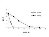
- FIG. 5 shows a process for supplying the reaction product with the thickness of the reaction product formed on the processing target S and energy for volatilizing the reaction product, and applying a bias voltage to the processing target S. Shows the relationship with time.
- the processing target S is a silicon substrate, and by exposing the processing target S to plasma generated from Ar gas, energy exceeding the volatilization of the reaction product is supplied to the reaction product. .
- FIG. 5 when the processing time is 0 second, application of energy for volatilizing the reaction product and application of a bias voltage are started simultaneously.
- the following effects can be obtained in addition to the effects (1) to (4) described above. it can. (5)
- a bias voltage to the processing target S, compared to a case where no bias voltage is applied to the processing target S, It is possible to increase the volatilization rate of the reaction product.
- the energy supply unit may supply the reaction product with more energy than volatilizing the reaction product by irradiating the processing target S with energy rays such as ultraviolet rays and electron beams.
- the energy supply unit may include a cooling unit that cools the processing target S.
- the temperature of the processing target S depends on the balance between the amount of heat given to the processing target S and the amount of heat taken by the cooling unit from the processing target S.
- the temperature that is lower than the temperature at which silicon and oxygen constituting the surface of the processing target S react in the air atmosphere may be used.
- the etchant supply unit may generate active species including hydrogen by an excitation unit other than the microwave source 17.
- Examples of the excitation unit include a configuration including a high-frequency antenna and a power source connected to the high-frequency antenna.
- the first gas supply unit 15A may supply the discharge tube 16 with a gas capable of generating plasma containing H * . Therefore, the first gas supply unit 15 ⁇ / b> A may supply a gas other than the NH 3 gas to the discharge tube 16. Examples of gases other than NH 3 gas include H 2 gas.
- fluorine may be supplied NF 3 gas other than the gas as the gas containing.
- gases other than NF 3 gas include F 2 gas.
- the third gas supply unit 15C is configured to supply a rare gas other than Ar gas such as helium (He) gas, neon (Ne) gas, krypton (Kr) gas, or xenon (Xe) gas in the vacuum chamber 11. May be supplied.
- a rare gas other than Ar gas such as helium (He) gas, neon (Ne) gas, krypton (Kr) gas, or xenon (Xe) gas in the vacuum chamber 11. May be supplied.
- the timing at which the third gas supply unit starts supplying Ar gas may not be the same as the timing at which the first gas supply unit and the second gas supply unit stop supplying gas.
- the timing at which the third gas supply unit starts supplying Ar gas may be after the timing at which the first gas supply unit and the second gas supply unit stop supplying gas.
- the high frequency antenna 18 may be located on the opposite side of the shower space 12 from the second space 11 ⁇ / b> B outside the vacuum chamber 11. That is, the high frequency antenna 18 may have a shape surrounding the first space 11 ⁇ / b> A outside the vacuum chamber 11. Even in this case, it is possible to generate plasma from the Ar gas supplied to the first space 11A by the third gas supply unit 15C. However, in order to make Ar + reach the processing target S before Ar +, which is one of the active species contained in Ar gas, is deactivated, the high-frequency antenna 18 is located outside the vacuum chamber 11 as described above. However, it is preferable to have a shape surrounding the second space 11B.
- the processing target S may be configured to include a silicon substrate and one or more insulating layers formed on the silicon substrate.
- the insulating layer only needs to have a through hole for exposing a part of the silicon substrate.
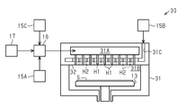
- the oxide film removing device 30 may include a shower plate 32 having a plurality of first holes H1 and a plurality of second holes H2.
- the first hole H1 connects the first space 31A and the second space 31B in the vacuum chamber 31.
- the second hole H2 connects the gas flow path 31C, which is a space independent from the first space 31A, and the second space 31B.
- the first gas supply unit 15A is connected to the discharge tube 16, and the discharge tube 16 supplies at least one of H * and NH 2 * from the first hole H1 toward the processing target S through the first space 31A.
- the second gas supply unit 15B supplies the NF 3 gas toward the processing target S from the second hole H2.
- the third gas supply unit 15 ⁇ / b> C is connected to the discharge tube 16. Thereby, radicals, such as Ar gas which 15 C of 3rd gas supply parts supply, can be supplied to the process target S. FIG. Therefore, the high frequency antenna 18 and the antenna high frequency power supply 19 can be omitted.
- the oxide film removing apparatus 30 including the shower plate 32 when used, the fluorine-containing gas and at least one of H * and NH 2 * are separately supplied to the shower plate 32. Then, an etchant is generated by separately diffusing a gas containing fluorine and at least one of H * and NH 2 * by the shower plate 32 and supplying the gas to the processing object S. Therefore, an etchant can be generated in the space on the processing target S.
- the first gas supply unit 15A, the second gas supply unit 15B, the discharge tube 16, the microwave source 17, and the shower plate 32 are included in the etchant supply unit.
- the oxide film removing apparatus 30 of this modification can be implemented in combination with the configuration of the oxide film removing apparatus 20 of the second embodiment. That is, the oxide film removing apparatus 30 may include a bias high-frequency power source 21.
- the oxide film removing apparatus 10 may include two or more vacuum chambers. In this case, the reaction for generating the reaction product is performed in one vacuum chamber, and the reaction product is removed in the other vacuum chamber.
Landscapes
- Physics & Mathematics (AREA)
- Engineering & Computer Science (AREA)
- Plasma & Fusion (AREA)
- Electromagnetism (AREA)
- Spectroscopy & Molecular Physics (AREA)
- Drying Of Semiconductors (AREA)
Abstract
Description
上記酸化膜除去装置において、前記エッチャント供給部は、フッ素を含むガスをシャワープレートに供給するフッ素ガス供給部と、水素ラジカルおよびアンモニアラジカルの少なくとも一方を前記フッ素を含むガスとは別々に前記シャワープレートに供給するラジカル供給部と、前記フッ素を含むガスと、前記水素ラジカルおよび前記アンモニアラジカルの少なくとも一方とを別々に前記処理対象に供給する前記シャワープレートと、を含んでもよい。
上記酸化膜除去装置はさらに、前記エネルギーを前記反応生成物に与える期間の少なくとも一部においてバイアス電圧を前記処理対象に印加するバイアス用高周波電源を含んでもよい。
図1から図3を参照して、酸化膜除去方法および酸化膜除去装置の第1実施形態を説明する。以下では、酸化膜除去装置の構成、および、酸化膜除去方法を順に説明する。
図1を参照して、酸化膜除去装置の構成を説明する。なお、図1に示される構成は、酸化膜除去装置の構成における一例である。
図2および図3を参照して、酸化膜除去方法を説明する。
酸化膜除去方法は、反応生成物を生成すること、および、反応生成物を除去することを含む。反応生成物を生成することは、処理対象Sのシリコン酸化膜に、フッ素と水素とを含むエッチャントを供給することによって、シリコン酸化膜よりも揮発性が高い反応生成物を生成することを含む。反応生成物を除去することは、反応生成物が揮発するためのエネルギーを反応生成物に与えることによって、処理対象S上から反応生成物を除去することを含む。反応生成物を除去することは、シリコン酸化膜が除去された後の処理対象Sにおける表面を形成するシリコンと酸素とが大気雰囲気において反応する温度未満に処理対象Sの温度を維持することを含む。以下、図2および図3を参照して、酸化膜除去方法をより詳しく説明する。以下では、酸化膜除去方法の一例として、図1を参照して説明した酸化膜除去装置10を用いて実施される方法を説明する。
(1)シリコン酸化膜が除去された後の処理対象Sを大気に暴露しても、処理対象Sの表面を形成するシリコンが酸化されること、言い換えれば、処理対象Sにシリコン酸化膜が形成されることが抑えられる。
(3)処理対象Sをプラズマに暴露することによって、反応生成物が揮発する程度に大きいエネルギーを反応生成物に与えつつ、処理対象Sの温度を大気中においてシリコンと酸素とが反応する未満の温度とすることができる。
図4および図5を参照して、酸化膜除去方法および酸化膜除去装置の第2実施形態を説明する。第2実施形態において、上述した第1実施形態に対して、酸化膜が除去される処理対象に高周波電圧を印加する点が異なっている。そのため以下では、こうした相違点を詳しく説明する一方で、第2実施形態において第1実施形態と共通する構成には、第1実施形態と同一の符号を付すことによって、当該構成の詳しい説明を省略する。以下では、酸化膜除去装置の構成と、酸化膜除去装置の作用とを順に説明する。
図4を参照して、酸化膜除去装置の構成を説明する。
図4が示すように、酸化膜除去装置20は、第1実施形態の酸化膜除去装置10の構成に加えて、さらにバイアス用高周波電源21を備えている。バイアス用高周波電源21は、支持部13、あるいは、支持部13内に位置する電極に電気的に接続されている。バイアス用高周波電源21は、支持部13あるいは電極に高周波電圧を印加することによって、支持部13に支持された処理対象Sにバイアス電圧を印加する。
図5を参照して、酸化膜除去装置20の作用を説明する。
図5は、処理対象S上に形成された反応生成物の厚さと、反応生成物を揮発させるためのエネルギーを反応生成物に供給し、かつ、バイアス電圧を処理対象Sに印加する処理を行った時間との関係を示している。なお、図5において、処理対象Sはシリコン基板であり、処理対象SをArガスから生成されたプラズマに暴露することによって、反応生成物を揮発させる以上のエネルギーを反応生成物に供給している。また、図5において、処理時間が0秒であるときに、反応生成物を揮発させるためのエネルギーの付与と、バイアス電圧の印加とが同時に開始されている。
(5)反応生成物を揮発させる以上のエネルギーを反応生成物に供給することに加えて、処理対象Sにバイアス電圧を印加することによって、処理対象Sにバイアス電圧を印加しない場合に比べて、反応生成物の揮発速度を高めることが可能である。
[エネルギー供給部]
・エネルギー供給部は、処理対象Sに対して紫外線、および、電子ビームなどのエネルギー線を照射することによって、反応生成物を揮発させる以上のエネルギーを反応生成物に供給してもよい。
・エッチャント供給部は、マイクロ波源17以外の励起部によって水素を含む活性種を生成してもよい。励起部には、例えば、高周波アンテナと、高周波アンテナに接続された電源とを含む構成を挙げることができる。
・第1ガス供給部15Aは、H*を含むプラズマを生成することが可能なガスを放電管16に供給すればよい。そのため、第1ガス供給部15Aは、NH3ガス以外のガスを放電管16に供給してもよい。NH3ガス以外のガスには、例えば、H2ガスなどを挙げることができる。
・第2ガス供給部15Bは、フッ素を含むガスとしてNF3ガス以外のガスを供給してもよい。NF3ガス以外のガスには、例えば、F2ガスなどを挙げることができる。
・第3ガス供給部15Cは、Arガス以外の希ガス例えば、ヘリウム(He)ガス、ネオン(Ne)ガス、クリプトン(Kr)ガス、および、キセノン(Xe)ガスのいずれかを真空槽11内に供給してもよい。
・高周波アンテナ18は、真空槽11よりも外側において、シャワープレート12に対して第2空間11Bとは反対側に位置してもよい。すなわち、高周波アンテナ18は、真空槽11よりも外側において、第1空間11Aを囲む形状を有してもよい。この場合であっても、第3ガス供給部15Cが第1空間11Aに供給したArガスからプラズマを生成することは可能である。ただし、Arガスに含まれる活性種の1つであるAr+が失活する前にAr+を処理対象Sに到達させる上では、上述したように、高周波アンテナ18は、真空槽11よりも外側において、第2空間11Bを囲む形状を有することが好ましい。
・処理対象Sは、シリコン基板と、シリコン基板上に形成された1つ以上の絶縁層を備える構成でもよい。この場合には、絶縁層が、シリコン基板の一部を露出させるための貫通孔を有していればよい。
・図6が示すように、酸化膜除去装置30は、複数の第1孔H1と複数の第2孔H2とを有するシャワープレート32を備えてもよい。第1孔H1は、真空槽31における第1空間31Aと第2空間31Bとを接続する。これに対して、第2孔H2は、第1空間31Aから独立した空間であるガス流路31Cと第2空間31Bとを接続する。
Claims (7)
- 処理対象に含まれるシリコン酸化膜に、フッ素と水素とを含むエッチャントを供給することによって、前記シリコン酸化膜よりも揮発性が高い反応生成物を生成することと、
前記反応生成物が揮発するためのエネルギーを前記反応生成物に与えることによって、前記処理対象上から前記反応生成物を除去することと、を含み、
前記反応生成物を除去することは、前記処理対象の温度を80℃未満に維持することを含む
酸化膜除去方法。 - 前記反応生成物を除去することは、希ガスから生成したプラズマに前記反応生成物が付着した前記処理対象を暴露することによって、前記反応生成物に前記エネルギーを与えることを含む
請求項1に記載の酸化膜除去方法。 - 前記反応生成物を生成することは、フッ素を含むガスと、水素ラジカルおよびアンモニアラジカルの少なくとも一方とを別々にシャワープレートに供給し、前記フッ素を含むガスと、前記水素ラジカルおよび前記アンモニアラジカルの少なくとも一方とを前記シャワープレートによって別々に拡散して前記処理対象に供給することによって前記エッチャントを生成することを含む
請求項1または2に記載の酸化膜除去方法。 - 前記反応生成物を除去することは、前記エネルギーを前記反応生成物に与える期間の少なくとも一部においてバイアス電圧を前記処理対象に印加することを含む、請求項1~3のいずれか一項に記載の酸化膜除去方法。
- シリコン酸化膜を有する処理対象を収容する真空槽と、
フッ素と水素とを含むエッチャントを前記シリコン酸化膜に供給するエッチャント供給部と、
前記エッチャントと前記シリコン酸化膜とから生成された反応生成物に、前記反応生成物が揮発するためのエネルギーを供給し、かつ、80℃未満の温度に前記処理対象を加熱する熱量を前記処理対象に供給するエネルギー供給部と、を備える
酸化膜除去装置。 - 前記エッチャント供給部は、
フッ素を含むガスをシャワープレートに供給するフッ素ガス供給部と、
水素ラジカルおよびアンモニアラジカルの少なくとも一方を前記フッ素を含むガスとは別々に前記シャワープレートに供給するラジカル供給部と、
前記フッ素を含むガスと、前記水素ラジカルおよび前記アンモニアラジカルの少なくとも一方とを別々に前記処理対象に供給する前記シャワープレートと、を含む
請求項5に記載の酸化膜除去装置。 - 前記エネルギーを前記反応生成物に与える期間の少なくとも一部においてバイアス電圧を前記処理対象に印加するバイアス用高周波電源をさらに含む
請求項5または6に記載の酸化膜除去装置。
Priority Applications (3)
| Application Number | Priority Date | Filing Date | Title |
|---|---|---|---|
| CN201980035215.8A CN112204713A (zh) | 2018-06-08 | 2019-05-20 | 氧化膜除去方法及氧化膜除去装置 |
| KR1020207034142A KR20210003230A (ko) | 2018-06-08 | 2019-05-20 | 산화막 제거 방법, 및 산화막 제거 장치 |
| JP2020523602A JPWO2019235196A1 (ja) | 2018-06-08 | 2019-05-20 | 酸化膜除去方法、および、酸化膜除去装置 |
Applications Claiming Priority (2)
| Application Number | Priority Date | Filing Date | Title |
|---|---|---|---|
| JP2018110335 | 2018-06-08 | ||
| JP2018-110335 | 2018-06-08 |
Publications (1)
| Publication Number | Publication Date |
|---|---|
| WO2019235196A1 true WO2019235196A1 (ja) | 2019-12-12 |
Family
ID=68770234
Family Applications (1)
| Application Number | Title | Priority Date | Filing Date |
|---|---|---|---|
| PCT/JP2019/019854 Ceased WO2019235196A1 (ja) | 2018-06-08 | 2019-05-20 | 酸化膜除去方法、および、酸化膜除去装置 |
Country Status (4)
| Country | Link |
|---|---|
| JP (1) | JPWO2019235196A1 (ja) |
| KR (1) | KR20210003230A (ja) |
| CN (1) | CN112204713A (ja) |
| WO (1) | WO2019235196A1 (ja) |
Citations (5)
| Publication number | Priority date | Publication date | Assignee | Title |
|---|---|---|---|---|
| JP2011508433A (ja) * | 2007-12-21 | 2011-03-10 | アプライド マテリアルズ インコーポレイテッド | 自然酸化物の成長を低減するためのプラズマクリーンプロセスによるパッシベーション層の形成 |
| US20160042968A1 (en) * | 2014-08-05 | 2016-02-11 | Applied Materials, Inc. | Integrated oxide and si etch for 3d cell channel mobility improvements |
| JP2016027594A (ja) * | 2014-07-01 | 2016-02-18 | 東京エレクトロン株式会社 | 被処理体を処理する方法 |
| JP2016134623A (ja) * | 2015-01-16 | 2016-07-25 | エーエスエム アイピー ホールディング ビー.ブイ. | プラスマエンハンスト原子層エッチングの方法 |
| JP2017208510A (ja) * | 2016-05-20 | 2017-11-24 | 東京エレクトロン株式会社 | エッチング方法 |
Family Cites Families (5)
| Publication number | Priority date | Publication date | Assignee | Title |
|---|---|---|---|---|
| JP4854317B2 (ja) * | 2006-01-31 | 2012-01-18 | 東京エレクトロン株式会社 | 基板処理方法 |
| JP2013038109A (ja) | 2011-08-03 | 2013-02-21 | Ulvac Japan Ltd | 酸化膜の除去方法及びバッチ式半導体デバイス製造装置 |
| JP6063181B2 (ja) * | 2012-08-29 | 2017-01-18 | 東京エレクトロン株式会社 | プラズマ処理方法、及びプラズマ処理装置 |
| JP6400425B2 (ja) * | 2014-10-15 | 2018-10-03 | 東京エレクトロン株式会社 | 多層膜をエッチングする方法 |
| JP6692202B2 (ja) * | 2016-04-08 | 2020-05-13 | 東京エレクトロン株式会社 | 基板処理方法及び基板処理装置 |
-
2019
- 2019-05-20 KR KR1020207034142A patent/KR20210003230A/ko not_active Abandoned
- 2019-05-20 JP JP2020523602A patent/JPWO2019235196A1/ja active Pending
- 2019-05-20 CN CN201980035215.8A patent/CN112204713A/zh active Pending
- 2019-05-20 WO PCT/JP2019/019854 patent/WO2019235196A1/ja not_active Ceased
Patent Citations (5)
| Publication number | Priority date | Publication date | Assignee | Title |
|---|---|---|---|---|
| JP2011508433A (ja) * | 2007-12-21 | 2011-03-10 | アプライド マテリアルズ インコーポレイテッド | 自然酸化物の成長を低減するためのプラズマクリーンプロセスによるパッシベーション層の形成 |
| JP2016027594A (ja) * | 2014-07-01 | 2016-02-18 | 東京エレクトロン株式会社 | 被処理体を処理する方法 |
| US20160042968A1 (en) * | 2014-08-05 | 2016-02-11 | Applied Materials, Inc. | Integrated oxide and si etch for 3d cell channel mobility improvements |
| JP2016134623A (ja) * | 2015-01-16 | 2016-07-25 | エーエスエム アイピー ホールディング ビー.ブイ. | プラスマエンハンスト原子層エッチングの方法 |
| JP2017208510A (ja) * | 2016-05-20 | 2017-11-24 | 東京エレクトロン株式会社 | エッチング方法 |
Also Published As
| Publication number | Publication date |
|---|---|
| JPWO2019235196A1 (ja) | 2021-06-17 |
| KR20210003230A (ko) | 2021-01-11 |
| CN112204713A (zh) | 2021-01-08 |
Similar Documents
| Publication | Publication Date | Title |
|---|---|---|
| CN110660663B (zh) | 蚀刻处理方法以及蚀刻处理装置 | |
| KR102364322B1 (ko) | 에칭 방법 | |
| US12087591B2 (en) | Plasma processing apparatus and system | |
| KR102364950B1 (ko) | 진공 배기 방법 및 진공 처리 장치 | |
| US10347499B2 (en) | Method for etching layer to be etched | |
| KR20160003565A (ko) | 피처리체를 처리하는 방법 | |
| JP2020136669A (ja) | エッチング方法 | |
| CN111048389B (zh) | 等离子体处理方法和等离子体处理装置 | |
| CN101950721B (zh) | 表面处理方法 | |
| KR20190031101A (ko) | 플라즈마 처리 방법 | |
| JP4256064B2 (ja) | プラズマ処理装置の制御方法 | |
| JP2012064773A (ja) | プラズマ処理装置 | |
| CN111681956B (zh) | 等离子体处理方法和等离子体处理装置 | |
| JPWO2019235196A1 (ja) | 酸化膜除去方法、および、酸化膜除去装置 | |
| JP7114384B2 (ja) | 酸化膜除去方法、および、酸化膜除去装置 | |
| JP7629594B2 (ja) | 成膜方法及び成膜装置 | |
| JP4480012B2 (ja) | エッチング方法およびエッチング装置 | |
| JP7348019B2 (ja) | エッチング方法、および、エッチング装置 | |
| JP7543059B2 (ja) | プラズマ処理装置、およびプラズマ処理方法 | |
| JP6259610B2 (ja) | プラズマ処理装置およびプラズマ処理方法 | |
| JPH08241886A (ja) | プラズマ処理方法 | |
| JP5324144B2 (ja) | プラズマ処理方法及び処理装置 | |
| JP2002285317A (ja) | アルマイト製品及びその表面処理方法 | |
| JPH05109675A (ja) | 電子ビーム励起ドライエツチング方法および装置 | |
| JP2003332317A (ja) | プラズマを用いたレジスト剥離装置及び方法 |
Legal Events
| Date | Code | Title | Description |
|---|---|---|---|
| 121 | Ep: the epo has been informed by wipo that ep was designated in this application |
Ref document number: 19815271 Country of ref document: EP Kind code of ref document: A1 |
|
| ENP | Entry into the national phase |
Ref document number: 20207034142 Country of ref document: KR Kind code of ref document: A |
|
| WWE | Wipo information: entry into national phase |
Ref document number: 2020523602 Country of ref document: JP |
|
| NENP | Non-entry into the national phase |
Ref country code: DE |
|
| 122 | Ep: pct application non-entry in european phase |
Ref document number: 19815271 Country of ref document: EP Kind code of ref document: A1 |