WO2019235154A1 - 表示装置 - Google Patents
表示装置 Download PDFInfo
- Publication number
- WO2019235154A1 WO2019235154A1 PCT/JP2019/019405 JP2019019405W WO2019235154A1 WO 2019235154 A1 WO2019235154 A1 WO 2019235154A1 JP 2019019405 W JP2019019405 W JP 2019019405W WO 2019235154 A1 WO2019235154 A1 WO 2019235154A1
- Authority
- WO
- WIPO (PCT)
- Prior art keywords
- region
- insulating layer
- layer
- organic
- wiring
- Prior art date
- Legal status (The legal status is an assumption and is not a legal conclusion. Google has not performed a legal analysis and makes no representation as to the accuracy of the status listed.)
- Ceased
Links
Images

Classifications
-
- H—ELECTRICITY
- H10—SEMICONDUCTOR DEVICES; ELECTRIC SOLID-STATE DEVICES NOT OTHERWISE PROVIDED FOR
- H10K—ORGANIC ELECTRIC SOLID-STATE DEVICES
- H10K59/00—Integrated devices, or assemblies of multiple devices, comprising at least one organic light-emitting element covered by group H10K50/00
- H10K59/10—OLED displays
- H10K59/12—Active-matrix OLED [AMOLED] displays
-
- G—PHYSICS
- G09—EDUCATION; CRYPTOGRAPHY; DISPLAY; ADVERTISING; SEALS
- G09F—DISPLAYING; ADVERTISING; SIGNS; LABELS OR NAME-PLATES; SEALS
- G09F9/00—Indicating arrangements for variable information in which the information is built-up on a support by selection or combination of individual elements
- G09F9/30—Indicating arrangements for variable information in which the information is built-up on a support by selection or combination of individual elements in which the desired character or characters are formed by combining individual elements
-
- H—ELECTRICITY
- H05—ELECTRIC TECHNIQUES NOT OTHERWISE PROVIDED FOR
- H05B—ELECTRIC HEATING; ELECTRIC LIGHT SOURCES NOT OTHERWISE PROVIDED FOR; CIRCUIT ARRANGEMENTS FOR ELECTRIC LIGHT SOURCES, IN GENERAL
- H05B33/00—Electroluminescent light sources
- H05B33/02—Details
-
- H—ELECTRICITY
- H05—ELECTRIC TECHNIQUES NOT OTHERWISE PROVIDED FOR
- H05B—ELECTRIC HEATING; ELECTRIC LIGHT SOURCES NOT OTHERWISE PROVIDED FOR; CIRCUIT ARRANGEMENTS FOR ELECTRIC LIGHT SOURCES, IN GENERAL
- H05B33/00—Electroluminescent light sources
- H05B33/02—Details
- H05B33/04—Sealing arrangements, e.g. against humidity
-
- H—ELECTRICITY
- H05—ELECTRIC TECHNIQUES NOT OTHERWISE PROVIDED FOR
- H05B—ELECTRIC HEATING; ELECTRIC LIGHT SOURCES NOT OTHERWISE PROVIDED FOR; CIRCUIT ARRANGEMENTS FOR ELECTRIC LIGHT SOURCES, IN GENERAL
- H05B33/00—Electroluminescent light sources
- H05B33/02—Details
- H05B33/06—Electrode terminals
-
- H—ELECTRICITY
- H05—ELECTRIC TECHNIQUES NOT OTHERWISE PROVIDED FOR
- H05B—ELECTRIC HEATING; ELECTRIC LIGHT SOURCES NOT OTHERWISE PROVIDED FOR; CIRCUIT ARRANGEMENTS FOR ELECTRIC LIGHT SOURCES, IN GENERAL
- H05B33/00—Electroluminescent light sources
- H05B33/12—Light sources with substantially two-dimensional radiating surfaces
- H05B33/22—Light sources with substantially two-dimensional radiating surfaces characterised by the chemical or physical composition or the arrangement of auxiliary dielectric or reflective layers
-
- H—ELECTRICITY
- H10—SEMICONDUCTOR DEVICES; ELECTRIC SOLID-STATE DEVICES NOT OTHERWISE PROVIDED FOR
- H10K—ORGANIC ELECTRIC SOLID-STATE DEVICES
- H10K59/00—Integrated devices, or assemblies of multiple devices, comprising at least one organic light-emitting element covered by group H10K50/00
- H10K59/10—OLED displays
- H10K59/12—Active-matrix OLED [AMOLED] displays
- H10K59/131—Interconnections, e.g. wiring lines or terminals
-
- H—ELECTRICITY
- H10—SEMICONDUCTOR DEVICES; ELECTRIC SOLID-STATE DEVICES NOT OTHERWISE PROVIDED FOR
- H10K—ORGANIC ELECTRIC SOLID-STATE DEVICES
- H10K59/00—Integrated devices, or assemblies of multiple devices, comprising at least one organic light-emitting element covered by group H10K50/00
- H10K59/80—Constructional details
- H10K59/87—Passivation; Containers; Encapsulations
- H10K59/873—Encapsulations
-
- H—ELECTRICITY
- H10—SEMICONDUCTOR DEVICES; ELECTRIC SOLID-STATE DEVICES NOT OTHERWISE PROVIDED FOR
- H10K—ORGANIC ELECTRIC SOLID-STATE DEVICES
- H10K59/00—Integrated devices, or assemblies of multiple devices, comprising at least one organic light-emitting element covered by group H10K50/00
- H10K59/10—OLED displays
- H10K59/12—Active-matrix OLED [AMOLED] displays
- H10K59/122—Pixel-defining structures or layers, e.g. banks
-
- H—ELECTRICITY
- H10—SEMICONDUCTOR DEVICES; ELECTRIC SOLID-STATE DEVICES NOT OTHERWISE PROVIDED FOR
- H10K—ORGANIC ELECTRIC SOLID-STATE DEVICES
- H10K59/00—Integrated devices, or assemblies of multiple devices, comprising at least one organic light-emitting element covered by group H10K50/00
- H10K59/10—OLED displays
- H10K59/12—Active-matrix OLED [AMOLED] displays
- H10K59/124—Insulating layers formed between TFT elements and OLED elements
-
- H—ELECTRICITY
- H10—SEMICONDUCTOR DEVICES; ELECTRIC SOLID-STATE DEVICES NOT OTHERWISE PROVIDED FOR
- H10K—ORGANIC ELECTRIC SOLID-STATE DEVICES
- H10K59/00—Integrated devices, or assemblies of multiple devices, comprising at least one organic light-emitting element covered by group H10K50/00
- H10K59/40—OLEDs integrated with touch screens
Definitions
- Embodiments of the present invention relate to a display device.
- a part of the display panel may be bent from the viewpoint of performance or design.
- the stress on the wiring increases.
- the wiring may be disconnected due to an impact due to contact with the wiring or a temperature change, and the reliability of the display device may be reduced.
- the purpose of this embodiment is to provide a display device with high reliability.
- a substrate having a first region having a display region, a second region having a mounting region, and a third region located between the first region and the second region;
- a first inorganic insulating layer provided on the substrate in the first region and the second region, and formed on the first inorganic insulating layer, the first region, the second region, and the first region
- a wiring extending over three regions, and a second inorganic insulating layer provided on the wiring, wherein the second inorganic insulating layer extends at least in a region overlapping with the first inorganic insulating layer.
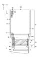
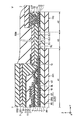
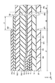
- FIG. 1 is a perspective view schematically showing a display device 1 according to the present embodiment.
- FIG. 2 is a diagram illustrating a state in which the bending area BA illustrated in FIG. 1 is bent.
- FIG. 3 is a cross-sectional view showing the display area DA shown in FIG. 4 is a cross-sectional view taken along the line IV-IV 'shown in FIG.
- FIG. 5 is a cross-sectional view taken along the line V-V ′ shown in FIG.
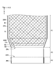
- FIG. 6 is an enlarged cross-sectional view showing the vicinity of the third region A3 shown in FIG.
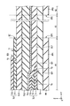
- FIG. 7 is a plan view showing a region where the insulating layer 11 and the inorganic layer 171 are provided.
- FIG. 8 is a cross-sectional view showing another example of the display panel 2.
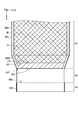
- FIG. 9 is a plan view of the display panel 2 shown in FIG.
- FIG. 10 is a cross-sectional view showing another example of the display panel 2.
- FIG. 11 is a plan view of
- FIG. 1 is a plan view schematically showing the display device 1 according to the present embodiment.
- the display device 1 is an organic EL display device having an organic electroluminescence (EL) element as an example.
- the display device 1 may be another display device such as a liquid crystal display device having a liquid crystal layer or an electronic paper type display device having an electrophoretic element.
- the first direction X, the second direction Y, and the third direction Z shown in the figure are orthogonal to each other. Note that the first direction X, the second direction Y, and the third direction Z may intersect at an angle other than 90 degrees.
- the direction toward the tip of the arrow indicating the third direction Z is defined as “up”, and the direction opposite from the tip of the arrow is defined as “down”.
- the second member above the first member and “the second member below the first member” the second member may be in contact with the first member and is located away from the first member. It may be. In the latter case, a third member may be interposed between the first member and the second member.
- observation position for observing the display device 1 is on the tip side of the arrow indicating the third direction Z, and from this observation position toward the XY plane defined by the first direction X and the second direction Y. This is called planar view.
- the display device 1 includes a display panel 2, a wiring board 3, and the like.
- the display panel 2 has a shape in which the length along the second direction Y is larger than the length along the first direction X.
- the display panel 2 has sides EX1 and EX2 along the first direction X, and a side EY along the second direction Y. Sides EX1 and EX2 are shorter than side EY. Further, the side EX1 is shorter than the side EX2.
- the display panel 2 has a display area DA for displaying an image and a non-display area NDA located outside the display area DA.
- the display area DA has a substantially rectangular shape having a pair of long sides along the second direction Y and a pair of short sides along the first direction X.
- the display area DA includes a plurality of pixels PX arranged in a matrix.
- the pixel PX includes an organic EL element, a switching element for driving the organic EL element, and the like.
- the display panel 2 has a mounting region MT including the terminal TE in the vicinity of the side EX1.
- the terminals TE and the pixels PX are one-to-one and are electrically connected by the wiring WL.
- the power supply potential and the signal potential supplied from the external device are supplied to each pixel PX via the terminal TE and the wiring WL.
- the display panel 2 has flexibility.
- the display panel 2 has a bent area BA in the non-display area NDA, as indicated by hatching in the drawing.
- the folding area BA corresponds to an area that is bent when the display device 1 is accommodated in a housing or the like.
- the folding area BA is located between the display area DA and the mounting area MT.
- the wiring WL electrically connects the pixel PX and the terminal TE through the bent area BA.
- the wiring board 3 is mounted in the mounting area MT.
- the wiring board 3 is electrically connected to the display panel 2 via the terminal TE.
- the wiring board 3 is a flexible printed circuit board, for example.
- the wiring substrate 3 is mounted with an IC chip 4 for driving the pixel PX.
- the IC chip 4 may be mounted on the display panel 2.
- the length of the side along the first direction X of the wiring board 3 is equal to the side EX1, but may be different.
- the display panel 2 has a first area A1, a second area A2, and a third area A3.
- the first area A1 includes the display area DA and corresponds to an area between the side EX2 and the bent area BA.
- the second area A2 includes the mounting area MT and corresponds to an area between the bent area BA and the side EX1.
- the third area A3 is an area between the first area A1 and the second area A2. In the illustrated example, the third area A3 corresponds to the bent area BA.
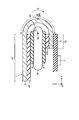
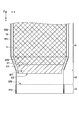
- FIG. 2 is a diagram showing a state where the folding area BA shown in FIG. 1 is bent.
- FIG. 2 shows a plane parallel to the YZ plane. Here, only the configuration necessary for the description is shown.
- the display device 1 includes a support substrate PP (PP1, PP2), a support member 50, an adhesive 51, and the like.
- the support substrate PP is provided on the surface opposite to the display surface of the display panel 2 except for the third region A3 (that is, the bent region BA).
- the first region A1 corresponds to a region where the support substrate PP1 is attached to the display panel 2.
- the second region A2 corresponds to a region where the support substrate PP2 is attached to the display panel 2.
- the third region A3 corresponds to a region where the support substrate PP is not provided, that is, a region between the support substrate PP1 and the support substrate PP2.
- the support substrate PP functions as a support layer that suppresses the bending of the display panel 2 in the display area DA and the mounting area MT, for example. Further, the support substrate PP has moisture resistance that suppresses intrusion of moisture and the like into the display panel 2 and gas barrier property that suppresses intrusion of gas, and also functions as a barrier layer.
- the support substrate PP is a film formed using polyethylene terephthalate. Note that another thin film may be interposed between the support substrate PP and the display panel 2.
- the display panel 2 is bent so as to sandwich the support member 50, and is attached to the support member 50 with an adhesive 51.
- the support substrates PP1 and PP2 and the adhesive 51 are in contact with each other.
- the wiring board 3 is located below the display panel 2 and faces the display panel 2 and the support member 50 substantially in parallel. Note that the support member 50 may be omitted.
- the bending area BA is bent around a bending axis AX along the first direction X.
- the third region A3 has a curved surface shape, and in one example, is curved along the circumference.
- a curved generatrix GN formed by the folding area BA is parallel to the folding axis AX. That is, the generatrix GN of the bending area BA is parallel to the first direction X.
- a direction from the first region A1 side to the second region A2 side along the curved surface of the bent region BA is defined as a circumferential direction C.
- the curvature radius R1 of the bending area BA is defined as a distance from the bending axis AX to the inner surface of the display panel 2, for example. In one example, the radius of curvature R1 is 0.3 mm.
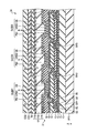
- FIG. 3 is a cross-sectional view showing the display area DA shown in FIG.
- the display panel 2 includes an insulating substrate 10, insulating layers 11 to 15, ribs 16, switching elements SW (SW1, SW2, SW3), organic EL elements OLED (OLED1, OLED2, OLED3), sealing film 17, adhesive layer 18, Optical elements OD1 and OD2 are provided.
- the support substrate PP ⁇ b> 1 is pasted under the insulating substrate 10.
- the insulating substrate 10 is made of an organic insulating material such as polyimide.
- the insulating layer 11 is formed on the insulating substrate 10.
- the insulating layer 11 may include a barrier layer for suppressing entry of moisture or the like from the insulating substrate 10 into the organic EL element OLED. Note that the insulating layer 11 may be omitted.
- the insulating substrate 10 may have a laminated structure including an inorganic insulating material sandwiched between organic insulating materials.
- the switching element SW is formed on the insulating layer 11.
- the switching element SW is configured by, for example, a thin film transistor (TFT).
- TFT thin film transistor
- the switching element SW is a top gate type, but may be a bottom gate type.
- the configuration of the switching element SW1 will be described as an example.
- the switching element SW1 includes a semiconductor layer SC, a gate electrode GE, a source electrode SE, and a drain electrode DE.
- the semiconductor layer SC is formed on the insulating layer 11 and covered with the insulating layer 12.
- the gate electrode GE is formed on the insulating layer 12 and is covered with the insulating layer 13.
- the source electrode SE and the drain electrode DE are each formed on the insulating layer 13.
- the source electrode SE and the drain electrode DE are in contact with the semiconductor layer SC in contact holes that penetrate the insulating layer 13 and the insulating layer 12 to the semiconductor layer SC, respectively.
- the gate electrode GE is formed of a metal material such as aluminum, titanium, silver, molybdenum, tungsten, copper, or chromium, or an alloy that combines these metal materials, and may have a single layer structure or a multilayer structure. There may be.
- the above metal materials can be applied as the material for forming the source electrode SE and the drain electrode DE.
- Each switching element SW is covered with an insulating layer 14.
- the insulating layer 14 is covered with the insulating layer 15.
- the insulating layers 11 to 13 and the insulating layer 15 are formed of an inorganic insulating material such as silicon oxide, silicon nitride, or silicon oxynitride.
- the insulating layer 14 is made of an organic insulating material such as polyimide, for example.
- the organic EL element OLED is formed on the insulating layer 15.
- the organic EL element OLED is a so-called top emission type that emits light to the side opposite to the insulating substrate 10, but is not limited to this example, and so-called bottom emission that emits light to the insulating substrate 10 side. It may be a type.
- the organic EL element OLED1 includes an organic light emitting layer ORG1 that emits red light
- the organic EL element OLED2 includes an organic light emitting layer ORG2 that emits blue light
- the organic EL element OLED3 emits an green light emitting layer. ORG3 is provided. Below, the structure is demonstrated taking the organic EL element OLED1 as an example.
- the organic EL element OLED1 includes a pixel electrode PE1, a common electrode CE, and an organic light emitting layer ORG1.
- the pixel electrode PE1 is provided on the insulating layer 15.
- the pixel electrode PE1 is in contact with the drain electrode DE of the switching element SW1 in a contact hole provided in the insulating layers 15 and 14. Thereby, the pixel electrode PE1 and the switching element SW1 are electrically connected to each other.
- the organic light emitting layer ORG1 is formed on the pixel electrode PE1.
- the organic light emitting layer ORG1 may further include an electron injection layer, a hole injection layer, an electron transport layer, a hole transport layer, and the like in order to improve the light emission efficiency.
- the common electrode CE is formed on the organic light emitting layer ORG1.
- the common electrode CE and the pixel electrode PE are formed of a transparent conductive material such as indium tin oxide (ITO) or indium zinc oxide (IZO).
- the organic EL element OLED1 configured as described above emits light with luminance according to a voltage (or current) applied between the pixel electrode PE1 and the common electrode CE. Although illustration is omitted, in the case of the top emission type, it is desirable that the organic EL element OLED1 includes a reflective layer between the insulating layer 15 and the pixel electrode PE1.
- the reflective layer is formed of a metal material having high reflectivity such as aluminum or silver.
- the reflective surface of the reflective layer that is, the surface on the organic light emitting layer ORG1 side may be flat, or irregularities may be formed to impart light scattering properties.
- Each organic EL element OLED is partitioned for each pixel PX by a rib 16 made of an organic insulating material.
- the rib 16 covers both ends of each pixel electrode PE and is in contact with the insulating layer 15.
- the rib 16 is made of polyimide, for example.
- the organic light emitting layers ORG1, ORG2, and ORG3 are in contact with the pixel electrodes PE1, PE2, and PE3, respectively, in regions where the ribs 16 are not provided.
- the common electrode CE is formed over the entire display area DA. That is, the common electrode CE is in contact with the organic light emitting layers ORG1, ORG2, and ORG3 and covers the ribs 16.
- the display panel 2 may have a common organic light emitting layer over the plurality of pixels PX.
- the display panel 2 includes a color filter at a position facing each organic EL element OLED.
- the color filter is formed of a resin material colored in red, green, blue, or the like, for example.
- the sealing film 17 covers the organic EL element OLED.
- the sealing film 17 suppresses intrusion of moisture and oxygen into the organic EL element OLED, and suppresses deterioration of the organic EL element OLED.
- the sealing film 17 includes an inorganic layer 171, an organic layer 172, and an inorganic layer 173.
- the inorganic layer 171 is formed on the organic EL element OLED.
- the inorganic layer 171 is in contact with the common electrode CE.
- the inorganic layer 173 is located above the inorganic layer 171.
- the organic layer 172 is located between the inorganic layer 171 and the inorganic layer 173 and is in contact with both the inorganic layer 171 and the inorganic layer 173.
- the inorganic layer 171 and the inorganic layer 173 mainly have a function of blocking moisture from entering the organic EL element OLED.
- the inorganic layer 171 and the inorganic layer 173 are transparent, and are formed of an inorganic insulating material such as silicon oxide, silicon nitride, or silicon oxynitride.
- the inorganic layer 171 and the inorganic layer 173 may be formed of the same material or different materials.
- the organic layer 172 is formed of a transparent organic insulating material.
- transparent means that the transmitted light is allowed to be colored within a range that does not affect the display.
- the optical elements OD1 and OD2 are provided on the sealing film 17.
- the optical element OD1 is an optical member such as a retardation plate.
- the optical element OD2 is an optical member such as a polarizing plate.
- the optical element OD1 is closer to the sealing film 17 than the optical element OD2, and is bonded to the sealing film 17 by the adhesive layer 18.
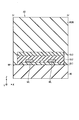
- FIG. 4 is a cross-sectional view taken along line IV-IV ′ shown in FIG. FIG. 4 shows a plane parallel to the XZ plane defined by the first direction X and the third direction Z.
- the display panel 2 includes organic layers OL1, OL2, OL3, and a resin layer RSN in addition to the insulating substrate 10 and the wiring WL.
- the organic layer OL1 is located on the insulating substrate 10.
- the wiring WL is located on the organic layer OL1 and is covered with the organic layer OL2.
- both ends of the organic layer OL1 are covered with the organic layer OL2. That is, the organic layer OL2 is in contact with the wiring WL and the organic layer OL1, and is also in contact with the insulating substrate 10 on both sides of the organic layer OL1.
- the organic layer OL3 is provided on the organic layer OL2.
- the resin layer RSN is provided on the organic layer OL3. In the illustrated example, the resin layer RSN is in contact with the insulating substrate 10 on both sides of the organic layers OL1, OL2, and OL3.
- the organic layers OL1, OL2, and OL3 are formed of an organic insulating material such as polyimide, for example.
- the organic layer OL1 and the organic layer OL2 are desirably formed of the same material.
- the organic layer OL3 may or may not contain fluorine.
- the resin layer RSN is an acrylic resin and is cured by irradiation with ultraviolet rays. Such a resin layer RSN functions as a protective layer for protecting the wiring WL.
- the Young's modulus of the organic layers OL1, OL2, and OL3 are all greater than the Young's modulus of the resin layer RSN.
- the neutral plane NP when the bent area BA is bent is located in the vicinity of the boundary between the insulating substrate 10 and the organic layer OL1, as indicated by a broken line in the drawing.
- the neutral surface NP is a surface where the tensile stress and the compressive stress are balanced when the folding area BA is bent.
- FIG. 5 is a cross-sectional view taken along the line V-V ′ shown in FIG. FIG. 5 shows a plane parallel to the YZ plane.
- the first region A1, the third region A3, and the second region A2 are arranged along the second direction Y in this order.
- the support substrate PP1 provided in the first region A1 is a support substrate PP that overlaps with the organic EL element OLED.
- the support substrate PP2 provided in the second region A2 is a support substrate PP that overlaps the terminal TE.
- the second direction Y corresponds to the circumferential direction C shown in FIG.
- the display panel 2 includes an insulating substrate 10, insulating layers 11 to 15, ribs 16, organic EL elements OLED, sealing film 17, adhesive layer 18, optical elements OD1 and OD2, wiring WL, organic layers OL1, OL2, and OL3, In addition to the terminal TE, the wiring GL and the conductive layer CL are provided.
- the insulating substrate 10 is provided over the first region A1, the second region A2, and the third region A3.
- the insulating layers 11 to 13 are provided in the first region A1 and the second region A2, but are not provided in the third region A3.
- the insulating layers 11 to 13 are removed in a region slightly wider than the third region A3. In other words, the insulating layers 11 to 13 are not provided at the end of the first region A1 on the third region A3 side and the end of the second region A2 on the third region A3 side.
- the insulating layer 11 extends further to the second region A2 side than the insulating layers 12 and 13.
- the insulating layer 11 extends further to the first region A1 side than the insulating layers 12 and 13.
- the wiring GL is located on the insulating layer 12 and covered with the insulating layer 13 in the first region A1.
- the wiring GL is electrically connected to the gate electrode GE of the switching element SW shown in FIG.
- Such a wiring GL can be formed with the same material and the same process as the gate electrode GE of the switching element SW shown in FIG. 3, for example.
- the wiring WL extends from the end of the first region A1 on the third region A3 side to the second region A2.
- the wiring WL is formed on the insulating layer 13 in the first region A1 and the second region A2, and is formed on the organic layer OL1 in the third region A3.
- the wiring WL is in contact with the wiring GL in the contact hole formed in the insulating layer 13.
- the wiring WL and the wiring GL are electrically connected.
- the wiring WL can be formed using the same material and the same process as the source electrode SE and the drain electrode DE of the switching element SW shown in FIG.
- the organic layer OL1 is provided at least in the third region A3. In the illustrated example, both end portions in the second direction Y of the organic layer OL1 are located in the first region A1 and the second region A2.
- the organic layer OL1 is formed on the insulating substrate 10 in the third region A3.
- the organic layer OL1 is formed on the insulating substrate 10 and covers a part of the insulating layers 11 to 13 in the first region A1 and the second region A2.
- the organic layer OL1 covers a part of the insulating layers 11 to 13 in the first region A1 and the second region A2, so that the step formed in the vicinity of the end portions of the insulating layers 11 to 13 is alleviated. Therefore, in the first region A1 and the second region A2, disconnection of the wiring WL formed on the insulating layer 13 and the organic layer OL1 can be suppressed.
- the organic layer OL2 is provided over the first region A1, the second region A2, and the third region A3, and covers the wiring WL.
- the organic layer OL2 covers the wiring WL in the first region A1 and the second region A2, and is in contact with the insulating layer 13 as well.
- the organic layer OL2 can be formed by the same material and the same process as the insulating layer 14, for example.
- the organic layer OL2 has a contact hole that exposes the wiring WL in the second region A2.
- the conductive layer CL is provided in the contact hole and is in contact with the wiring WL.
- the conductive layer CL can be formed, for example, with the same material and the same process as the pixel electrode PE.
- the organic layer OL3 is provided in a region overlapping with the organic layer OL2. That is, the organic layer OL3 is provided over the first region A1, the second region A2, and the third region A3.
- the organic layer OL3 can be formed by the same material and the same process as the rib 16, for example.
- the organic layer OL3 has a contact hole that exposes the conductive layer CL in the second region A2.
- the terminal TE is provided in the contact hole and is in contact with the conductive layer CL. Thereby, the terminal TE and the wiring WL are electrically connected via the conductive layer CL.
- the terminal TE can be formed at the same time as the common electrode CE, for example. In the illustrated example, the terminal TE is electrically connected to the wiring board 3 via the anisotropic conductive film ACF.
- the insulating layer 14 is provided in the first region A1, and is located on the side farther from the second region A2 than the wiring WL.
- the insulating layer 14 has a groove 14 ⁇ / b> T that exposes the insulating layer 13.
- the groove 14T moisture permeation through the insulating layer 14 from the second region A2 side to the first region A1 side is suppressed, and deterioration of the organic EL element OLED is suppressed.
- a crack is generated in the inorganic layers 171 and 173, which will be described later, when the third region A3 is bent, the display of the crack is caused by the formation of the groove 14T and the unevenness resulting therefrom. Propagation to the area DA side can be suppressed.
- Such a groove 14T is preferably formed in an annular shape surrounding the display area DA in plan view.
- the insulating layer 15 is provided in the first region A1 and covers the entire insulating layer 14. That is, the insulating layer 15 is in contact with the insulating layer 13 in the groove 14T, extends to the second region A2 side from the insulating layer 14, and is in contact with the insulating layer 13.
- the organic EL element OLED and the rib 16 are located in a region inside the groove 14T, that is, a side farther from the second region A2 than the groove 14T (or the display region DA side).
- the sealing film 17 is provided in the first region A1, and a part thereof extends to the second region A2 side with respect to the insulating layer 14. More specifically, the inorganic layer 171 in the sealing film 17 extends to the second region A2 side with respect to the insulating layer 14, and is in contact with the organic layers OL2 and OL3. In the illustrated example, the inorganic layer 171 covers the side surfaces of the organic layers OL2 and OL3 and extends to above the organic layer OL3.
- the organic layer 172 of the sealing film 17 is provided in a region overlapping with the insulating layer 14. Of the sealing film 17, the inorganic layer 173 extends toward the second region A ⁇ b> 2 with respect to the organic layer 172, and is in contact with the inorganic layer 171.
- the inorganic layers 171 and 173 extend at least in a region overlapping with the inorganic layers located below the wiring WL, that is, the insulating layers 11 to 13. In one example, both of the inorganic layers 171 and 173 extend to the second region A2 side with respect to the insulating layers 11 to 13.
- the insulating layers 11 to 13 and the inorganic layers 171 and 173 overlap the optical elements OD1 and OD2, and extend to the second region A2 side from the optical elements OD1 and OD2.
- the wiring WL and the organic layers OL2 and OL3 are arranged in a region closer to the second region A2 than the optical elements OD1 and OD2.
- the wiring WL does not overlap with the optical elements OD1 and OD2, but the ends of the organic layers OL2 and OL3 on the organic EL element OLED side overlap with the optical elements OD1 and OD2.
- the wiring WL and the organic layers OL2 and OL3 are sandwiched between the insulating layers 11 to 13 and the inorganic layers 171 and 173.
- the resin layer RSN is provided over the first region A1, the second region A2, and the third region A3.
- the resin layer RSN covers the organic layer OL3 and the inorganic layers 171 and 173, and is in contact with the adhesive layer 18 and the optical elements OD1 and OD2.
- the resin layer RSN covers the organic layer OL3 and the wiring board 3.
- the resin layer RSN covers the organic layer OL3.
- a crosslinking agent may be added to at least the organic layer OL1 and the resin layer RSN among the organic layers OL1, OL2, and OL3 and the resin layer RSN.
- the display panel has a multilayer structure including various conductive layers such as wiring and various insulating layers. For this reason, in the bent region where the display panel is deformed to have a curvature, if the adhesion between the layers is weak, peeling between the layers due to bending or a crack accompanying the peeling may occur. is there. Particularly, since stress due to bending is likely to be applied to the starting point of bending (in the present embodiment, in the vicinity of the boundary between the first region A1 and the third region A3), layer peeling is likely to occur. Such a peeled portion can be a moisture intrusion path into the display panel.
- the organic layer OL1 contains a crosslinking agent
- the adhesion between the organic layer OL1 and the insulating substrate 10 is improved.
- the crosslinking agent is contained in the resin layer RSN
- the adhesion between the resin layer RSN and the organic layer OL3 is improved.
- the resin layer RSN contains a cross-linking agent
- the adhesion between the resin layer RSN and the optical elements OD1 and OD2, the adhesive layer 18, and the inorganic layers 171 and 173 is also improved in the first region A1. . Therefore, peeling of the resin layer RSN can be suppressed in the vicinity of the bending start point in the first region A1. As a result, a decrease in reliability of the display device 1 can be suppressed.
- FIG. 6 is an enlarged sectional view showing the vicinity of the third region A3 shown in FIG.
- the support substrate PP1 has an end EP1 on the second region A2 side.
- the support substrate PP2 has an end portion EP2 on the first region A1 side.
- the third region A3 corresponds to a region between the end portion EP1 and the end portion EP2.
- both the end portion EI2 of the inorganic layer 171 and the end portion EI3 of the inorganic layer 173 are in the second region than both the end portion EI1 of the insulating layer 11 and the end portions EI4 of the insulating layers 12 and 13. Close to A2.
- both the end portions EI1 and EI4 overlap with the inorganic layers 171 and 173.
- the end portions EI1, EI2, EI3, and EI4 are end portions on the second region A2 side.
- the end portions EI1, EI2, EI3, and EI4 are located in the first region A1. That is, the end portions EI1, EI2, EI3, and EI4 are further away from the second region A2 than the end portion EP1.
- the position of the end EI2 and the position of the end EI3 are aligned in the second direction Y.
- the position of the end portion EI2 and the position of the end portion EI3 may be aligned with the position of the end portion EI1.
- the end portion EI1 is closer to the second region A2 than the end portion EI4.
- the end of the insulating layer 12 and the end of the insulating layer 13 are aligned, but may not be aligned. In this case, the end portion of the insulating layer 12 is closer to the second region A2 than the end portion of the insulating layer 13.
- the insulating layers 11 to 13 are preferably formed of silicon oxide. Since silicon oxide has a larger tensile stress than silicon nitride, generation of cracks when the third region A3 is bent can be suppressed.
- FIG. 7 is a plan view showing a region where the insulating layer 11 and the inorganic layer 171 are provided.
- the insulating layer 11 is provided over substantially the entire first region A1.
- the inorganic layer 171 is provided at least in a region overlapping with the insulating layer 11, and in this embodiment, extends to the second region A2 side from the insulating layer 11. I'm out. That is, the end portion EI2 is closer to the second region A2 than the end portion EI1.
- the end portions EI1 and EI2 extend along the first direction X in one example.
- the support substrate PP substantially overlaps the insulating substrate 10 except for the third region A3. That is, the shape of the support substrate PP1 is substantially equal to the shape of the first region A1, and the shape of the support substrate PP2 is substantially equal to the shape of the second region A2.
- the end portion EP1 of the support substrate PP1 and the end portion EP2 of the support substrate PP2 extend along the first direction X.
- the end portions EI1 and EI2 are located between the end portion EOD of the optical element OD2 and the end portion EP1 of the support substrate PP1.
- the inorganic layers 171 and 173 extend at least in the region where the insulating layers 11 to 13 are provided.
- the elastic modulus of the inorganic layer is higher than that of the organic layer. Therefore, by laminating the insulating layers 11 to 13 made of an inorganic layer and the inorganic layers 171 and 173 in the first region A1, the rigidity of the first region A1 can be increased.
- the insulating layers 11 to 13 and the inorganic layers 171 and 173 are not provided in the third region A3. For this reason, the rigidity of the third area A3 is lower than the rigidity of the first area A1.
- the first region A1 which is an originally unfolded region
- the wiring WL may be disconnected also in the first region A1.
- the inorganic layers 171 and 173 in the region overlapping the insulating layers 11 to 13 in the first region A1
- the bending rigidity of the third region A3 that is the bending region BA is reduced.
- the bending rigidity of the first region A1 can be increased.
- the bending of the first region A1 when the third region A3 is bent can be suppressed, and the disconnection of the wiring WL in the first region A1 can be suppressed.
- the two organic layers OL2 and OL3 are stacked on the wiring WL, and the inorganic layers 171 and 173 are provided on the organic layer OL3.
- the inorganic layers 171 and 173 having a large elastic modulus are arranged above the wiring WL (on the outer peripheral side when bent).
- the position of the neutral plane NP when the third region A3 is bent can be brought closer to the wiring WL. Therefore, the stress in the vicinity of the wiring WL when the third region A3 is bent can be relaxed, and breakage of the wiring WL can be suppressed.
- the display device 1 capable of improving the reliability is provided.
- another example of the display panel 2 will be described with reference to FIGS. 8 to 11.
- FIG. 8 is a cross-sectional view showing another example of the display panel 2.
- FIG. 9 is a plan view of the display panel 2 shown in FIG.
- the example shown in FIGS. 8 and 9 is different from the example shown in FIGS. 6 and 7 in that the inorganic layer 171 extends to the second region A2 side than the inorganic layer 173.
- the inorganic layer 171 is provided over the entire first region A1. That is, in the second direction Y, the position of the end portion EI2 and the position of the end portion EP1 are aligned.
- the insulating layers 11, 12, and 13 located below the wiring WL are regarded as the insulating layer IL1
- the inorganic layers 171 and 173 located above the wiring WL are regarded as the insulating layer IL2.
- the insulating layer IL2 is thin in the vicinity of the third region A3.
- the thickness T1 on the third region A3 side of the insulating layer IL2 is smaller than the thickness T2 on the side away from the third region A3 (that is, the organic EL element OLED side).
- the thickness T1 corresponds to the thickness of the inorganic layer 171 and the thickness T2 corresponds to the total thickness of the inorganic layers 171 and 173.
- the thickness T1 is 200 nm or less.
- the thickness of the inorganic layer 173 is equal to the thickness T1, but may be different.
- the insulating layer 11 extends to the second region A2 side from the insulating layers 12 and 13, the insulating layer IL1 is thin in the vicinity of the third region A3.
- the thickness T3 on the third region A3 side of the insulating layer IL1 is smaller than the thickness T4 on the side away from the third region A3.
- the thickness T3 corresponds to the thickness of the insulating layer 11
- the thickness T4 corresponds to the total thickness of the insulating layers 11, 12, and 13.
- the thickness T3 is 200 nm or less.
- each of the thickness of the insulating layer 12 and the thickness of the insulating layer 13 is equal to the thickness T3, but may be different.
- both the insulating layer IL2 located above the wiring WL and the insulating layer IL1 located below the wiring WL are thin in the vicinity of the third area A3 that is the bent area BA, and the third area A3. It is thicker on the side away from it.
- the greater the thickness of the inorganic layer the greater the amount of strain when the inorganic layer is bent, and cracks are more likely to occur in the inorganic layer.
- the thickness of the insulating layer IL1 and the thickness of the IL2 are reduced, so that the first Generation of cracks in the insulating layers IL1 and IL2 when the three regions A3 are bent can be suppressed.
- the inorganic layer 171 is provided in the whole 1st area
- FIG. 10 is a cross-sectional view showing another example of the display panel 2.
- FIG. 11 is a plan view of the display panel 2 shown in FIG.
- the example shown in FIGS. 10 and 11 is different from the example shown in FIGS. 8 and 9 in that the inorganic layer 171 extends to the third region A3. That is, the end portion EI2 is located in the third region A3.
- the length L1 of the inorganic layer 171 extending to the third region A3 is set so that the strain amount when the third region A3 is bent is 4% or less.
- the inorganic layer 173 is provided over the entire first region A1. That is, in the second direction Y, the position of the end portion EI3 and the position of the end portion EP1 are aligned. Note that the end portion EI3 does not need to exceed the third region A3 toward the second region A2, and may be positioned between the end portion EI1 and the end portion EP1 in the second direction Y.
- the same effect as the example shown in FIGS. 8 and 9 can be obtained.
- both the inorganic layer 171 and the inorganic layer 173 are provided in the whole 1st area
- the inorganic layer 171 is provided in the third region A3, the position of the neutral plane NP in the third region A3 can be brought closer to the wiring WL. Therefore, disconnection of the wiring WL when the third region A3 is bent can be suppressed.
- the organic EL display device having the organic EL element OLED has been described as an example.
- the present embodiment is also applicable to a liquid crystal display device having a liquid crystal layer.
- the display device is a liquid crystal display device, for example, an effect similar to the above effect can be obtained by extending an inorganic insulating layer provided between the pixel electrode and the common electrode to the bent area BA side.
- the present embodiment is applicable to a flexible substrate that includes a functional element such as a sensor but does not include a display element.
- the insulating layer 11 corresponds to the first inorganic insulating layer
- the inorganic layer 171 corresponds to the second inorganic insulating layer
- the inorganic layer 173 corresponds to the third inorganic insulating layer
- the insulating layer Reference numeral 12 corresponds to a fourth inorganic insulating layer.
- the end portion EI1 corresponds to a first end portion
- the end portion EI2 corresponds to a second end portion.
- the end portion EP1 of the support substrate PP1 corresponds to a third end portion.
- the organic layer OL1 corresponds to a first organic insulating layer
- the organic layer OL2 corresponds to a second organic insulating layer
- the organic layer OL3 corresponds to a third organic insulating layer.
Landscapes
- Engineering & Computer Science (AREA)
- Microelectronics & Electronic Packaging (AREA)
- Physics & Mathematics (AREA)
- General Physics & Mathematics (AREA)
- Theoretical Computer Science (AREA)
- Electroluminescent Light Sources (AREA)
- Devices For Indicating Variable Information By Combining Individual Elements (AREA)
Priority Applications (3)
| Application Number | Priority Date | Filing Date | Title |
|---|---|---|---|
| US16/953,628 US11849609B2 (en) | 2018-06-06 | 2020-11-20 | Display device |
| US18/503,242 US12171123B2 (en) | 2018-06-06 | 2023-11-07 | Display device |
| US18/944,458 US20250072243A1 (en) | 2018-06-06 | 2024-11-12 | Display device |
Applications Claiming Priority (2)
| Application Number | Priority Date | Filing Date | Title |
|---|---|---|---|
| JP2018108798A JP7098425B2 (ja) | 2018-06-06 | 2018-06-06 | 表示装置 |
| JP2018-108798 | 2018-06-06 |
Related Child Applications (1)
| Application Number | Title | Priority Date | Filing Date |
|---|---|---|---|
| US16/953,628 Continuation US11849609B2 (en) | 2018-06-06 | 2020-11-20 | Display device |
Publications (1)
| Publication Number | Publication Date |
|---|---|
| WO2019235154A1 true WO2019235154A1 (ja) | 2019-12-12 |
Family
ID=68770127
Family Applications (1)
| Application Number | Title | Priority Date | Filing Date |
|---|---|---|---|
| PCT/JP2019/019405 Ceased WO2019235154A1 (ja) | 2018-06-06 | 2019-05-15 | 表示装置 |
Country Status (3)
| Country | Link |
|---|---|
| US (3) | US11849609B2 (enExample) |
| JP (1) | JP7098425B2 (enExample) |
| WO (1) | WO2019235154A1 (enExample) |
Cited By (1)
| Publication number | Priority date | Publication date | Assignee | Title |
|---|---|---|---|---|
| CN115275045A (zh) * | 2022-07-19 | 2022-11-01 | 武汉华星光电半导体显示技术有限公司 | 显示面板及显示终端 |
Families Citing this family (5)
| Publication number | Priority date | Publication date | Assignee | Title |
|---|---|---|---|---|
| JP7098425B2 (ja) * | 2018-06-06 | 2022-07-11 | 株式会社ジャパンディスプレイ | 表示装置 |
| CN110634402A (zh) * | 2019-08-28 | 2019-12-31 | 武汉华星光电半导体显示技术有限公司 | 显示面板及其折弯方法及显示装置 |
| CN115777125B (zh) * | 2020-07-20 | 2025-10-10 | 夏普株式会社 | 显示装置 |
| CN115482721A (zh) * | 2021-05-31 | 2022-12-16 | 京东方科技集团股份有限公司 | 柔性显示面板和滑卷显示装置 |
| KR102891078B1 (ko) * | 2021-12-15 | 2025-11-24 | 엘지디스플레이 주식회사 | 표시 장치 |
Citations (4)
| Publication number | Priority date | Publication date | Assignee | Title |
|---|---|---|---|---|
| US20160174304A1 (en) * | 2014-12-10 | 2016-06-16 | Lg Display Co., Ltd. | Flexible display device with multiple types of micro-coating layers |
| JP2017111435A (ja) * | 2015-12-15 | 2017-06-22 | エルジー ディスプレイ カンパニー リミテッド | フレキシブル表示装置 |
| US20170237025A1 (en) * | 2016-02-12 | 2017-08-17 | Samsung Display Co., Ltd. | Display device |
| US20170262109A1 (en) * | 2016-03-11 | 2017-09-14 | Samsung Display Co., Ltd. | Display apparatus and method of manufacturing the same |
Family Cites Families (4)
| Publication number | Priority date | Publication date | Assignee | Title |
|---|---|---|---|---|
| EP3000659A1 (en) | 2014-09-26 | 2016-03-30 | Manucher Azmudeh | Interior rear view mirror assembly |
| JP6396879B2 (ja) | 2015-11-20 | 2018-09-26 | 株式会社ジャパンディスプレイ | 表示装置 |
| KR102597681B1 (ko) | 2016-09-19 | 2023-11-06 | 삼성디스플레이 주식회사 | 표시 장치 |
| JP7098425B2 (ja) * | 2018-06-06 | 2022-07-11 | 株式会社ジャパンディスプレイ | 表示装置 |
-
2018
- 2018-06-06 JP JP2018108798A patent/JP7098425B2/ja active Active
-
2019
- 2019-05-15 WO PCT/JP2019/019405 patent/WO2019235154A1/ja not_active Ceased
-
2020
- 2020-11-20 US US16/953,628 patent/US11849609B2/en active Active
-
2023
- 2023-11-07 US US18/503,242 patent/US12171123B2/en active Active
-
2024
- 2024-11-12 US US18/944,458 patent/US20250072243A1/en active Pending
Patent Citations (4)
| Publication number | Priority date | Publication date | Assignee | Title |
|---|---|---|---|---|
| US20160174304A1 (en) * | 2014-12-10 | 2016-06-16 | Lg Display Co., Ltd. | Flexible display device with multiple types of micro-coating layers |
| JP2017111435A (ja) * | 2015-12-15 | 2017-06-22 | エルジー ディスプレイ カンパニー リミテッド | フレキシブル表示装置 |
| US20170237025A1 (en) * | 2016-02-12 | 2017-08-17 | Samsung Display Co., Ltd. | Display device |
| US20170262109A1 (en) * | 2016-03-11 | 2017-09-14 | Samsung Display Co., Ltd. | Display apparatus and method of manufacturing the same |
Cited By (1)
| Publication number | Priority date | Publication date | Assignee | Title |
|---|---|---|---|---|
| CN115275045A (zh) * | 2022-07-19 | 2022-11-01 | 武汉华星光电半导体显示技术有限公司 | 显示面板及显示终端 |
Also Published As
| Publication number | Publication date |
|---|---|
| US20250072243A1 (en) | 2025-02-27 |
| US20210074795A1 (en) | 2021-03-11 |
| JP7098425B2 (ja) | 2022-07-11 |
| US12171123B2 (en) | 2024-12-17 |
| US11849609B2 (en) | 2023-12-19 |
| JP2019211676A (ja) | 2019-12-12 |
| US20240074264A1 (en) | 2024-02-29 |
Similar Documents
| Publication | Publication Date | Title |
|---|---|---|
| KR102636836B1 (ko) | 표시 장치 | |
| JP7098425B2 (ja) | 表示装置 | |
| US10754463B2 (en) | Display device having shaped sealing member | |
| CN107819006B (zh) | 显示装置 | |
| US11653531B2 (en) | Transparent display device having display area including transmissive area and non-transmissive area | |
| US10840463B2 (en) | Display device | |
| JP7077001B2 (ja) | 表示装置 | |
| US20180175324A1 (en) | Display device having a protection layer | |
| KR20170071662A (ko) | 가요성 표시 장치 | |
| US10268092B2 (en) | Display device | |
| US10636989B2 (en) | Display device including an insulating substrate with pixels disposed on a first surface | |
| CN116419599A (zh) | 显示装置 | |
| CN120344098A (zh) | 显示设备及制造显示设备的方法 | |
| JP2019003142A (ja) | 表示装置 | |
| US11758754B2 (en) | Display apparatus | |
| KR102392175B1 (ko) | 플렉서블 장치 | |
| KR102769474B1 (ko) | 표시 장치 | |
| TWI862190B (zh) | 可撓顯示裝置 | |
| JP2018156850A (ja) | 表示装置 | |
| KR20250047452A (ko) | 표시 장치 | |
| KR20240038891A (ko) | 표시 장치 | |
| JP2019159280A (ja) | 電気光学装置及び偏光板 | |
| KR20080057892A (ko) | 표시 장치 |
Legal Events
| Date | Code | Title | Description |
|---|---|---|---|
| 121 | Ep: the epo has been informed by wipo that ep was designated in this application |
Ref document number: 19814164 Country of ref document: EP Kind code of ref document: A1 |
|
| NENP | Non-entry into the national phase |
Ref country code: DE |
|
| 122 | Ep: pct application non-entry in european phase |
Ref document number: 19814164 Country of ref document: EP Kind code of ref document: A1 |