WO2019235154A1 - Display device - Google Patents
Display device Download PDFInfo
- Publication number
- WO2019235154A1 WO2019235154A1 PCT/JP2019/019405 JP2019019405W WO2019235154A1 WO 2019235154 A1 WO2019235154 A1 WO 2019235154A1 JP 2019019405 W JP2019019405 W JP 2019019405W WO 2019235154 A1 WO2019235154 A1 WO 2019235154A1
- Authority
- WO
- WIPO (PCT)
- Prior art keywords
- region
- insulating layer
- layer
- organic
- wiring
- Prior art date
Links
Images

Classifications
-
- H—ELECTRICITY
- H10—SEMICONDUCTOR DEVICES; ELECTRIC SOLID-STATE DEVICES NOT OTHERWISE PROVIDED FOR
- H10K—ORGANIC ELECTRIC SOLID-STATE DEVICES
- H10K59/00—Integrated devices, or assemblies of multiple devices, comprising at least one organic light-emitting element covered by group H10K50/00
- H10K59/10—OLED displays
- H10K59/12—Active-matrix OLED [AMOLED] displays
- H10K59/131—Interconnections, e.g. wiring lines or terminals
-
- G—PHYSICS
- G09—EDUCATION; CRYPTOGRAPHY; DISPLAY; ADVERTISING; SEALS
- G09F—DISPLAYING; ADVERTISING; SIGNS; LABELS OR NAME-PLATES; SEALS
- G09F9/00—Indicating arrangements for variable information in which the information is built-up on a support by selection or combination of individual elements
- G09F9/30—Indicating arrangements for variable information in which the information is built-up on a support by selection or combination of individual elements in which the desired character or characters are formed by combining individual elements
-
- H—ELECTRICITY
- H05—ELECTRIC TECHNIQUES NOT OTHERWISE PROVIDED FOR
- H05B—ELECTRIC HEATING; ELECTRIC LIGHT SOURCES NOT OTHERWISE PROVIDED FOR; CIRCUIT ARRANGEMENTS FOR ELECTRIC LIGHT SOURCES, IN GENERAL
- H05B33/00—Electroluminescent light sources
- H05B33/02—Details
-
- H—ELECTRICITY
- H05—ELECTRIC TECHNIQUES NOT OTHERWISE PROVIDED FOR
- H05B—ELECTRIC HEATING; ELECTRIC LIGHT SOURCES NOT OTHERWISE PROVIDED FOR; CIRCUIT ARRANGEMENTS FOR ELECTRIC LIGHT SOURCES, IN GENERAL
- H05B33/00—Electroluminescent light sources
- H05B33/02—Details
- H05B33/04—Sealing arrangements, e.g. against humidity
-
- H—ELECTRICITY
- H05—ELECTRIC TECHNIQUES NOT OTHERWISE PROVIDED FOR
- H05B—ELECTRIC HEATING; ELECTRIC LIGHT SOURCES NOT OTHERWISE PROVIDED FOR; CIRCUIT ARRANGEMENTS FOR ELECTRIC LIGHT SOURCES, IN GENERAL
- H05B33/00—Electroluminescent light sources
- H05B33/02—Details
- H05B33/06—Electrode terminals
-
- H—ELECTRICITY
- H05—ELECTRIC TECHNIQUES NOT OTHERWISE PROVIDED FOR
- H05B—ELECTRIC HEATING; ELECTRIC LIGHT SOURCES NOT OTHERWISE PROVIDED FOR; CIRCUIT ARRANGEMENTS FOR ELECTRIC LIGHT SOURCES, IN GENERAL
- H05B33/00—Electroluminescent light sources
- H05B33/12—Light sources with substantially two-dimensional radiating surfaces
- H05B33/22—Light sources with substantially two-dimensional radiating surfaces characterised by the chemical or physical composition or the arrangement of auxiliary dielectric or reflective layers
-
- H—ELECTRICITY
- H10—SEMICONDUCTOR DEVICES; ELECTRIC SOLID-STATE DEVICES NOT OTHERWISE PROVIDED FOR
- H10K—ORGANIC ELECTRIC SOLID-STATE DEVICES
- H10K50/00—Organic light-emitting devices
-
- H—ELECTRICITY
- H10—SEMICONDUCTOR DEVICES; ELECTRIC SOLID-STATE DEVICES NOT OTHERWISE PROVIDED FOR
- H10K—ORGANIC ELECTRIC SOLID-STATE DEVICES
- H10K50/00—Organic light-emitting devices
- H10K50/80—Constructional details
- H10K50/84—Passivation; Containers; Encapsulations
- H10K50/844—Encapsulations
-
- H—ELECTRICITY
- H10—SEMICONDUCTOR DEVICES; ELECTRIC SOLID-STATE DEVICES NOT OTHERWISE PROVIDED FOR
- H10K—ORGANIC ELECTRIC SOLID-STATE DEVICES
- H10K59/00—Integrated devices, or assemblies of multiple devices, comprising at least one organic light-emitting element covered by group H10K50/00
- H10K59/10—OLED displays
- H10K59/12—Active-matrix OLED [AMOLED] displays
- H10K59/122—Pixel-defining structures or layers, e.g. banks
-
- H—ELECTRICITY
- H10—SEMICONDUCTOR DEVICES; ELECTRIC SOLID-STATE DEVICES NOT OTHERWISE PROVIDED FOR
- H10K—ORGANIC ELECTRIC SOLID-STATE DEVICES
- H10K59/00—Integrated devices, or assemblies of multiple devices, comprising at least one organic light-emitting element covered by group H10K50/00
- H10K59/10—OLED displays
- H10K59/12—Active-matrix OLED [AMOLED] displays
- H10K59/124—Insulating layers formed between TFT elements and OLED elements
-
- H—ELECTRICITY
- H10—SEMICONDUCTOR DEVICES; ELECTRIC SOLID-STATE DEVICES NOT OTHERWISE PROVIDED FOR
- H10K—ORGANIC ELECTRIC SOLID-STATE DEVICES
- H10K59/00—Integrated devices, or assemblies of multiple devices, comprising at least one organic light-emitting element covered by group H10K50/00
- H10K59/40—OLEDs integrated with touch screens
Definitions
- Embodiments of the present invention relate to a display device.
- a part of the display panel may be bent from the viewpoint of performance or design.
- the stress on the wiring increases.
- the wiring may be disconnected due to an impact due to contact with the wiring or a temperature change, and the reliability of the display device may be reduced.
- the purpose of this embodiment is to provide a display device with high reliability.
- a substrate having a first region having a display region, a second region having a mounting region, and a third region located between the first region and the second region;
- a first inorganic insulating layer provided on the substrate in the first region and the second region, and formed on the first inorganic insulating layer, the first region, the second region, and the first region
- a wiring extending over three regions, and a second inorganic insulating layer provided on the wiring, wherein the second inorganic insulating layer extends at least in a region overlapping with the first inorganic insulating layer.
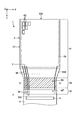
- FIG. 1 is a perspective view schematically showing a display device 1 according to the present embodiment.
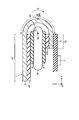
- FIG. 2 is a diagram illustrating a state in which the bending area BA illustrated in FIG. 1 is bent.
- FIG. 3 is a cross-sectional view showing the display area DA shown in FIG. 4 is a cross-sectional view taken along the line IV-IV 'shown in FIG.
- FIG. 5 is a cross-sectional view taken along the line V-V ′ shown in FIG.
- FIG. 6 is an enlarged cross-sectional view showing the vicinity of the third region A3 shown in FIG.
- FIG. 7 is a plan view showing a region where the insulating layer 11 and the inorganic layer 171 are provided.
- FIG. 8 is a cross-sectional view showing another example of the display panel 2.
- FIG. 9 is a plan view of the display panel 2 shown in FIG.
- FIG. 10 is a cross-sectional view showing another example of the display panel 2.
- FIG. 11 is a plan view of
- FIG. 1 is a plan view schematically showing the display device 1 according to the present embodiment.
- the display device 1 is an organic EL display device having an organic electroluminescence (EL) element as an example.
- the display device 1 may be another display device such as a liquid crystal display device having a liquid crystal layer or an electronic paper type display device having an electrophoretic element.
- the first direction X, the second direction Y, and the third direction Z shown in the figure are orthogonal to each other. Note that the first direction X, the second direction Y, and the third direction Z may intersect at an angle other than 90 degrees.
- the direction toward the tip of the arrow indicating the third direction Z is defined as “up”, and the direction opposite from the tip of the arrow is defined as “down”.
- the second member above the first member and “the second member below the first member” the second member may be in contact with the first member and is located away from the first member. It may be. In the latter case, a third member may be interposed between the first member and the second member.
- observation position for observing the display device 1 is on the tip side of the arrow indicating the third direction Z, and from this observation position toward the XY plane defined by the first direction X and the second direction Y. This is called planar view.
- the display device 1 includes a display panel 2, a wiring board 3, and the like.
- the display panel 2 has a shape in which the length along the second direction Y is larger than the length along the first direction X.
- the display panel 2 has sides EX1 and EX2 along the first direction X, and a side EY along the second direction Y. Sides EX1 and EX2 are shorter than side EY. Further, the side EX1 is shorter than the side EX2.
- the display panel 2 has a display area DA for displaying an image and a non-display area NDA located outside the display area DA.
- the display area DA has a substantially rectangular shape having a pair of long sides along the second direction Y and a pair of short sides along the first direction X.
- the display area DA includes a plurality of pixels PX arranged in a matrix.
- the pixel PX includes an organic EL element, a switching element for driving the organic EL element, and the like.
- the display panel 2 has a mounting region MT including the terminal TE in the vicinity of the side EX1.
- the terminals TE and the pixels PX are one-to-one and are electrically connected by the wiring WL.
- the power supply potential and the signal potential supplied from the external device are supplied to each pixel PX via the terminal TE and the wiring WL.
- the display panel 2 has flexibility.
- the display panel 2 has a bent area BA in the non-display area NDA, as indicated by hatching in the drawing.
- the folding area BA corresponds to an area that is bent when the display device 1 is accommodated in a housing or the like.
- the folding area BA is located between the display area DA and the mounting area MT.
- the wiring WL electrically connects the pixel PX and the terminal TE through the bent area BA.
- the wiring board 3 is mounted in the mounting area MT.
- the wiring board 3 is electrically connected to the display panel 2 via the terminal TE.
- the wiring board 3 is a flexible printed circuit board, for example.
- the wiring substrate 3 is mounted with an IC chip 4 for driving the pixel PX.
- the IC chip 4 may be mounted on the display panel 2.
- the length of the side along the first direction X of the wiring board 3 is equal to the side EX1, but may be different.
- the display panel 2 has a first area A1, a second area A2, and a third area A3.
- the first area A1 includes the display area DA and corresponds to an area between the side EX2 and the bent area BA.
- the second area A2 includes the mounting area MT and corresponds to an area between the bent area BA and the side EX1.
- the third area A3 is an area between the first area A1 and the second area A2. In the illustrated example, the third area A3 corresponds to the bent area BA.
- FIG. 2 is a diagram showing a state where the folding area BA shown in FIG. 1 is bent.
- FIG. 2 shows a plane parallel to the YZ plane. Here, only the configuration necessary for the description is shown.
- the display device 1 includes a support substrate PP (PP1, PP2), a support member 50, an adhesive 51, and the like.
- the support substrate PP is provided on the surface opposite to the display surface of the display panel 2 except for the third region A3 (that is, the bent region BA).
- the first region A1 corresponds to a region where the support substrate PP1 is attached to the display panel 2.
- the second region A2 corresponds to a region where the support substrate PP2 is attached to the display panel 2.
- the third region A3 corresponds to a region where the support substrate PP is not provided, that is, a region between the support substrate PP1 and the support substrate PP2.
- the support substrate PP functions as a support layer that suppresses the bending of the display panel 2 in the display area DA and the mounting area MT, for example. Further, the support substrate PP has moisture resistance that suppresses intrusion of moisture and the like into the display panel 2 and gas barrier property that suppresses intrusion of gas, and also functions as a barrier layer.
- the support substrate PP is a film formed using polyethylene terephthalate. Note that another thin film may be interposed between the support substrate PP and the display panel 2.
- the display panel 2 is bent so as to sandwich the support member 50, and is attached to the support member 50 with an adhesive 51.
- the support substrates PP1 and PP2 and the adhesive 51 are in contact with each other.
- the wiring board 3 is located below the display panel 2 and faces the display panel 2 and the support member 50 substantially in parallel. Note that the support member 50 may be omitted.
- the bending area BA is bent around a bending axis AX along the first direction X.
- the third region A3 has a curved surface shape, and in one example, is curved along the circumference.
- a curved generatrix GN formed by the folding area BA is parallel to the folding axis AX. That is, the generatrix GN of the bending area BA is parallel to the first direction X.
- a direction from the first region A1 side to the second region A2 side along the curved surface of the bent region BA is defined as a circumferential direction C.
- the curvature radius R1 of the bending area BA is defined as a distance from the bending axis AX to the inner surface of the display panel 2, for example. In one example, the radius of curvature R1 is 0.3 mm.
- FIG. 3 is a cross-sectional view showing the display area DA shown in FIG.
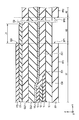
- the display panel 2 includes an insulating substrate 10, insulating layers 11 to 15, ribs 16, switching elements SW (SW1, SW2, SW3), organic EL elements OLED (OLED1, OLED2, OLED3), sealing film 17, adhesive layer 18, Optical elements OD1 and OD2 are provided.
- the support substrate PP ⁇ b> 1 is pasted under the insulating substrate 10.
- the insulating substrate 10 is made of an organic insulating material such as polyimide.
- the insulating layer 11 is formed on the insulating substrate 10.
- the insulating layer 11 may include a barrier layer for suppressing entry of moisture or the like from the insulating substrate 10 into the organic EL element OLED. Note that the insulating layer 11 may be omitted.
- the insulating substrate 10 may have a laminated structure including an inorganic insulating material sandwiched between organic insulating materials.
- the switching element SW is formed on the insulating layer 11.
- the switching element SW is configured by, for example, a thin film transistor (TFT).
- TFT thin film transistor
- the switching element SW is a top gate type, but may be a bottom gate type.
- the configuration of the switching element SW1 will be described as an example.
- the switching element SW1 includes a semiconductor layer SC, a gate electrode GE, a source electrode SE, and a drain electrode DE.
- the semiconductor layer SC is formed on the insulating layer 11 and covered with the insulating layer 12.
- the gate electrode GE is formed on the insulating layer 12 and is covered with the insulating layer 13.
- the source electrode SE and the drain electrode DE are each formed on the insulating layer 13.
- the source electrode SE and the drain electrode DE are in contact with the semiconductor layer SC in contact holes that penetrate the insulating layer 13 and the insulating layer 12 to the semiconductor layer SC, respectively.
- the gate electrode GE is formed of a metal material such as aluminum, titanium, silver, molybdenum, tungsten, copper, or chromium, or an alloy that combines these metal materials, and may have a single layer structure or a multilayer structure. There may be.
- the above metal materials can be applied as the material for forming the source electrode SE and the drain electrode DE.
- Each switching element SW is covered with an insulating layer 14.
- the insulating layer 14 is covered with the insulating layer 15.
- the insulating layers 11 to 13 and the insulating layer 15 are formed of an inorganic insulating material such as silicon oxide, silicon nitride, or silicon oxynitride.
- the insulating layer 14 is made of an organic insulating material such as polyimide, for example.
- the organic EL element OLED is formed on the insulating layer 15.
- the organic EL element OLED is a so-called top emission type that emits light to the side opposite to the insulating substrate 10, but is not limited to this example, and so-called bottom emission that emits light to the insulating substrate 10 side. It may be a type.
- the organic EL element OLED1 includes an organic light emitting layer ORG1 that emits red light
- the organic EL element OLED2 includes an organic light emitting layer ORG2 that emits blue light
- the organic EL element OLED3 emits an green light emitting layer. ORG3 is provided. Below, the structure is demonstrated taking the organic EL element OLED1 as an example.
- the organic EL element OLED1 includes a pixel electrode PE1, a common electrode CE, and an organic light emitting layer ORG1.
- the pixel electrode PE1 is provided on the insulating layer 15.
- the pixel electrode PE1 is in contact with the drain electrode DE of the switching element SW1 in a contact hole provided in the insulating layers 15 and 14. Thereby, the pixel electrode PE1 and the switching element SW1 are electrically connected to each other.
- the organic light emitting layer ORG1 is formed on the pixel electrode PE1.
- the organic light emitting layer ORG1 may further include an electron injection layer, a hole injection layer, an electron transport layer, a hole transport layer, and the like in order to improve the light emission efficiency.
- the common electrode CE is formed on the organic light emitting layer ORG1.
- the common electrode CE and the pixel electrode PE are formed of a transparent conductive material such as indium tin oxide (ITO) or indium zinc oxide (IZO).
- the organic EL element OLED1 configured as described above emits light with luminance according to a voltage (or current) applied between the pixel electrode PE1 and the common electrode CE. Although illustration is omitted, in the case of the top emission type, it is desirable that the organic EL element OLED1 includes a reflective layer between the insulating layer 15 and the pixel electrode PE1.
- the reflective layer is formed of a metal material having high reflectivity such as aluminum or silver.
- the reflective surface of the reflective layer that is, the surface on the organic light emitting layer ORG1 side may be flat, or irregularities may be formed to impart light scattering properties.
- Each organic EL element OLED is partitioned for each pixel PX by a rib 16 made of an organic insulating material.
- the rib 16 covers both ends of each pixel electrode PE and is in contact with the insulating layer 15.
- the rib 16 is made of polyimide, for example.
- the organic light emitting layers ORG1, ORG2, and ORG3 are in contact with the pixel electrodes PE1, PE2, and PE3, respectively, in regions where the ribs 16 are not provided.
- the common electrode CE is formed over the entire display area DA. That is, the common electrode CE is in contact with the organic light emitting layers ORG1, ORG2, and ORG3 and covers the ribs 16.
- the display panel 2 may have a common organic light emitting layer over the plurality of pixels PX.
- the display panel 2 includes a color filter at a position facing each organic EL element OLED.
- the color filter is formed of a resin material colored in red, green, blue, or the like, for example.
- the sealing film 17 covers the organic EL element OLED.
- the sealing film 17 suppresses intrusion of moisture and oxygen into the organic EL element OLED, and suppresses deterioration of the organic EL element OLED.
- the sealing film 17 includes an inorganic layer 171, an organic layer 172, and an inorganic layer 173.
- the inorganic layer 171 is formed on the organic EL element OLED.
- the inorganic layer 171 is in contact with the common electrode CE.
- the inorganic layer 173 is located above the inorganic layer 171.
- the organic layer 172 is located between the inorganic layer 171 and the inorganic layer 173 and is in contact with both the inorganic layer 171 and the inorganic layer 173.
- the inorganic layer 171 and the inorganic layer 173 mainly have a function of blocking moisture from entering the organic EL element OLED.
- the inorganic layer 171 and the inorganic layer 173 are transparent, and are formed of an inorganic insulating material such as silicon oxide, silicon nitride, or silicon oxynitride.
- the inorganic layer 171 and the inorganic layer 173 may be formed of the same material or different materials.
- the organic layer 172 is formed of a transparent organic insulating material.
- transparent means that the transmitted light is allowed to be colored within a range that does not affect the display.
- the optical elements OD1 and OD2 are provided on the sealing film 17.
- the optical element OD1 is an optical member such as a retardation plate.
- the optical element OD2 is an optical member such as a polarizing plate.
- the optical element OD1 is closer to the sealing film 17 than the optical element OD2, and is bonded to the sealing film 17 by the adhesive layer 18.
- FIG. 4 is a cross-sectional view taken along line IV-IV ′ shown in FIG. FIG. 4 shows a plane parallel to the XZ plane defined by the first direction X and the third direction Z.
- the display panel 2 includes organic layers OL1, OL2, OL3, and a resin layer RSN in addition to the insulating substrate 10 and the wiring WL.
- the organic layer OL1 is located on the insulating substrate 10.
- the wiring WL is located on the organic layer OL1 and is covered with the organic layer OL2.
- both ends of the organic layer OL1 are covered with the organic layer OL2. That is, the organic layer OL2 is in contact with the wiring WL and the organic layer OL1, and is also in contact with the insulating substrate 10 on both sides of the organic layer OL1.
- the organic layer OL3 is provided on the organic layer OL2.
- the resin layer RSN is provided on the organic layer OL3. In the illustrated example, the resin layer RSN is in contact with the insulating substrate 10 on both sides of the organic layers OL1, OL2, and OL3.
- the organic layers OL1, OL2, and OL3 are formed of an organic insulating material such as polyimide, for example.
- the organic layer OL1 and the organic layer OL2 are desirably formed of the same material.
- the organic layer OL3 may or may not contain fluorine.
- the resin layer RSN is an acrylic resin and is cured by irradiation with ultraviolet rays. Such a resin layer RSN functions as a protective layer for protecting the wiring WL.
- the Young's modulus of the organic layers OL1, OL2, and OL3 are all greater than the Young's modulus of the resin layer RSN.
- the neutral plane NP when the bent area BA is bent is located in the vicinity of the boundary between the insulating substrate 10 and the organic layer OL1, as indicated by a broken line in the drawing.
- the neutral surface NP is a surface where the tensile stress and the compressive stress are balanced when the folding area BA is bent.
- FIG. 5 is a cross-sectional view taken along the line V-V ′ shown in FIG. FIG. 5 shows a plane parallel to the YZ plane.
- the first region A1, the third region A3, and the second region A2 are arranged along the second direction Y in this order.
- the support substrate PP1 provided in the first region A1 is a support substrate PP that overlaps with the organic EL element OLED.
- the support substrate PP2 provided in the second region A2 is a support substrate PP that overlaps the terminal TE.
- the second direction Y corresponds to the circumferential direction C shown in FIG.
- the display panel 2 includes an insulating substrate 10, insulating layers 11 to 15, ribs 16, organic EL elements OLED, sealing film 17, adhesive layer 18, optical elements OD1 and OD2, wiring WL, organic layers OL1, OL2, and OL3, In addition to the terminal TE, the wiring GL and the conductive layer CL are provided.
- the insulating substrate 10 is provided over the first region A1, the second region A2, and the third region A3.
- the insulating layers 11 to 13 are provided in the first region A1 and the second region A2, but are not provided in the third region A3.
- the insulating layers 11 to 13 are removed in a region slightly wider than the third region A3. In other words, the insulating layers 11 to 13 are not provided at the end of the first region A1 on the third region A3 side and the end of the second region A2 on the third region A3 side.
- the insulating layer 11 extends further to the second region A2 side than the insulating layers 12 and 13.
- the insulating layer 11 extends further to the first region A1 side than the insulating layers 12 and 13.
- the wiring GL is located on the insulating layer 12 and covered with the insulating layer 13 in the first region A1.
- the wiring GL is electrically connected to the gate electrode GE of the switching element SW shown in FIG.
- Such a wiring GL can be formed with the same material and the same process as the gate electrode GE of the switching element SW shown in FIG. 3, for example.
- the wiring WL extends from the end of the first region A1 on the third region A3 side to the second region A2.
- the wiring WL is formed on the insulating layer 13 in the first region A1 and the second region A2, and is formed on the organic layer OL1 in the third region A3.
- the wiring WL is in contact with the wiring GL in the contact hole formed in the insulating layer 13.
- the wiring WL and the wiring GL are electrically connected.
- the wiring WL can be formed using the same material and the same process as the source electrode SE and the drain electrode DE of the switching element SW shown in FIG.
- the organic layer OL1 is provided at least in the third region A3. In the illustrated example, both end portions in the second direction Y of the organic layer OL1 are located in the first region A1 and the second region A2.
- the organic layer OL1 is formed on the insulating substrate 10 in the third region A3.
- the organic layer OL1 is formed on the insulating substrate 10 and covers a part of the insulating layers 11 to 13 in the first region A1 and the second region A2.
- the organic layer OL1 covers a part of the insulating layers 11 to 13 in the first region A1 and the second region A2, so that the step formed in the vicinity of the end portions of the insulating layers 11 to 13 is alleviated. Therefore, in the first region A1 and the second region A2, disconnection of the wiring WL formed on the insulating layer 13 and the organic layer OL1 can be suppressed.
- the organic layer OL2 is provided over the first region A1, the second region A2, and the third region A3, and covers the wiring WL.
- the organic layer OL2 covers the wiring WL in the first region A1 and the second region A2, and is in contact with the insulating layer 13 as well.
- the organic layer OL2 can be formed by the same material and the same process as the insulating layer 14, for example.
- the organic layer OL2 has a contact hole that exposes the wiring WL in the second region A2.
- the conductive layer CL is provided in the contact hole and is in contact with the wiring WL.
- the conductive layer CL can be formed, for example, with the same material and the same process as the pixel electrode PE.
- the organic layer OL3 is provided in a region overlapping with the organic layer OL2. That is, the organic layer OL3 is provided over the first region A1, the second region A2, and the third region A3.
- the organic layer OL3 can be formed by the same material and the same process as the rib 16, for example.
- the organic layer OL3 has a contact hole that exposes the conductive layer CL in the second region A2.
- the terminal TE is provided in the contact hole and is in contact with the conductive layer CL. Thereby, the terminal TE and the wiring WL are electrically connected via the conductive layer CL.
- the terminal TE can be formed at the same time as the common electrode CE, for example. In the illustrated example, the terminal TE is electrically connected to the wiring board 3 via the anisotropic conductive film ACF.
- the insulating layer 14 is provided in the first region A1, and is located on the side farther from the second region A2 than the wiring WL.
- the insulating layer 14 has a groove 14 ⁇ / b> T that exposes the insulating layer 13.
- the groove 14T moisture permeation through the insulating layer 14 from the second region A2 side to the first region A1 side is suppressed, and deterioration of the organic EL element OLED is suppressed.
- a crack is generated in the inorganic layers 171 and 173, which will be described later, when the third region A3 is bent, the display of the crack is caused by the formation of the groove 14T and the unevenness resulting therefrom. Propagation to the area DA side can be suppressed.
- Such a groove 14T is preferably formed in an annular shape surrounding the display area DA in plan view.
- the insulating layer 15 is provided in the first region A1 and covers the entire insulating layer 14. That is, the insulating layer 15 is in contact with the insulating layer 13 in the groove 14T, extends to the second region A2 side from the insulating layer 14, and is in contact with the insulating layer 13.
- the organic EL element OLED and the rib 16 are located in a region inside the groove 14T, that is, a side farther from the second region A2 than the groove 14T (or the display region DA side).
- the sealing film 17 is provided in the first region A1, and a part thereof extends to the second region A2 side with respect to the insulating layer 14. More specifically, the inorganic layer 171 in the sealing film 17 extends to the second region A2 side with respect to the insulating layer 14, and is in contact with the organic layers OL2 and OL3. In the illustrated example, the inorganic layer 171 covers the side surfaces of the organic layers OL2 and OL3 and extends to above the organic layer OL3.
- the organic layer 172 of the sealing film 17 is provided in a region overlapping with the insulating layer 14. Of the sealing film 17, the inorganic layer 173 extends toward the second region A ⁇ b> 2 with respect to the organic layer 172, and is in contact with the inorganic layer 171.
- the inorganic layers 171 and 173 extend at least in a region overlapping with the inorganic layers located below the wiring WL, that is, the insulating layers 11 to 13. In one example, both of the inorganic layers 171 and 173 extend to the second region A2 side with respect to the insulating layers 11 to 13.
- the insulating layers 11 to 13 and the inorganic layers 171 and 173 overlap the optical elements OD1 and OD2, and extend to the second region A2 side from the optical elements OD1 and OD2.
- the wiring WL and the organic layers OL2 and OL3 are arranged in a region closer to the second region A2 than the optical elements OD1 and OD2.
- the wiring WL does not overlap with the optical elements OD1 and OD2, but the ends of the organic layers OL2 and OL3 on the organic EL element OLED side overlap with the optical elements OD1 and OD2.
- the wiring WL and the organic layers OL2 and OL3 are sandwiched between the insulating layers 11 to 13 and the inorganic layers 171 and 173.
- the resin layer RSN is provided over the first region A1, the second region A2, and the third region A3.
- the resin layer RSN covers the organic layer OL3 and the inorganic layers 171 and 173, and is in contact with the adhesive layer 18 and the optical elements OD1 and OD2.
- the resin layer RSN covers the organic layer OL3 and the wiring board 3.
- the resin layer RSN covers the organic layer OL3.
- a crosslinking agent may be added to at least the organic layer OL1 and the resin layer RSN among the organic layers OL1, OL2, and OL3 and the resin layer RSN.
- the display panel has a multilayer structure including various conductive layers such as wiring and various insulating layers. For this reason, in the bent region where the display panel is deformed to have a curvature, if the adhesion between the layers is weak, peeling between the layers due to bending or a crack accompanying the peeling may occur. is there. Particularly, since stress due to bending is likely to be applied to the starting point of bending (in the present embodiment, in the vicinity of the boundary between the first region A1 and the third region A3), layer peeling is likely to occur. Such a peeled portion can be a moisture intrusion path into the display panel.
- the organic layer OL1 contains a crosslinking agent
- the adhesion between the organic layer OL1 and the insulating substrate 10 is improved.
- the crosslinking agent is contained in the resin layer RSN
- the adhesion between the resin layer RSN and the organic layer OL3 is improved.
- the resin layer RSN contains a cross-linking agent
- the adhesion between the resin layer RSN and the optical elements OD1 and OD2, the adhesive layer 18, and the inorganic layers 171 and 173 is also improved in the first region A1. . Therefore, peeling of the resin layer RSN can be suppressed in the vicinity of the bending start point in the first region A1. As a result, a decrease in reliability of the display device 1 can be suppressed.
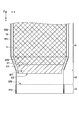
- FIG. 6 is an enlarged sectional view showing the vicinity of the third region A3 shown in FIG.
- the support substrate PP1 has an end EP1 on the second region A2 side.
- the support substrate PP2 has an end portion EP2 on the first region A1 side.
- the third region A3 corresponds to a region between the end portion EP1 and the end portion EP2.
- both the end portion EI2 of the inorganic layer 171 and the end portion EI3 of the inorganic layer 173 are in the second region than both the end portion EI1 of the insulating layer 11 and the end portions EI4 of the insulating layers 12 and 13. Close to A2.
- both the end portions EI1 and EI4 overlap with the inorganic layers 171 and 173.
- the end portions EI1, EI2, EI3, and EI4 are end portions on the second region A2 side.
- the end portions EI1, EI2, EI3, and EI4 are located in the first region A1. That is, the end portions EI1, EI2, EI3, and EI4 are further away from the second region A2 than the end portion EP1.
- the position of the end EI2 and the position of the end EI3 are aligned in the second direction Y.
- the position of the end portion EI2 and the position of the end portion EI3 may be aligned with the position of the end portion EI1.
- the end portion EI1 is closer to the second region A2 than the end portion EI4.
- the end of the insulating layer 12 and the end of the insulating layer 13 are aligned, but may not be aligned. In this case, the end portion of the insulating layer 12 is closer to the second region A2 than the end portion of the insulating layer 13.
- the insulating layers 11 to 13 are preferably formed of silicon oxide. Since silicon oxide has a larger tensile stress than silicon nitride, generation of cracks when the third region A3 is bent can be suppressed.
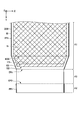
- FIG. 7 is a plan view showing a region where the insulating layer 11 and the inorganic layer 171 are provided.
- the insulating layer 11 is provided over substantially the entire first region A1.
- the inorganic layer 171 is provided at least in a region overlapping with the insulating layer 11, and in this embodiment, extends to the second region A2 side from the insulating layer 11. I'm out. That is, the end portion EI2 is closer to the second region A2 than the end portion EI1.
- the end portions EI1 and EI2 extend along the first direction X in one example.
- the support substrate PP substantially overlaps the insulating substrate 10 except for the third region A3. That is, the shape of the support substrate PP1 is substantially equal to the shape of the first region A1, and the shape of the support substrate PP2 is substantially equal to the shape of the second region A2.
- the end portion EP1 of the support substrate PP1 and the end portion EP2 of the support substrate PP2 extend along the first direction X.
- the end portions EI1 and EI2 are located between the end portion EOD of the optical element OD2 and the end portion EP1 of the support substrate PP1.
- the inorganic layers 171 and 173 extend at least in the region where the insulating layers 11 to 13 are provided.
- the elastic modulus of the inorganic layer is higher than that of the organic layer. Therefore, by laminating the insulating layers 11 to 13 made of an inorganic layer and the inorganic layers 171 and 173 in the first region A1, the rigidity of the first region A1 can be increased.
- the insulating layers 11 to 13 and the inorganic layers 171 and 173 are not provided in the third region A3. For this reason, the rigidity of the third area A3 is lower than the rigidity of the first area A1.
- the first region A1 which is an originally unfolded region
- the wiring WL may be disconnected also in the first region A1.
- the inorganic layers 171 and 173 in the region overlapping the insulating layers 11 to 13 in the first region A1
- the bending rigidity of the third region A3 that is the bending region BA is reduced.
- the bending rigidity of the first region A1 can be increased.
- the bending of the first region A1 when the third region A3 is bent can be suppressed, and the disconnection of the wiring WL in the first region A1 can be suppressed.
- the two organic layers OL2 and OL3 are stacked on the wiring WL, and the inorganic layers 171 and 173 are provided on the organic layer OL3.
- the inorganic layers 171 and 173 having a large elastic modulus are arranged above the wiring WL (on the outer peripheral side when bent).
- the position of the neutral plane NP when the third region A3 is bent can be brought closer to the wiring WL. Therefore, the stress in the vicinity of the wiring WL when the third region A3 is bent can be relaxed, and breakage of the wiring WL can be suppressed.
- the display device 1 capable of improving the reliability is provided.
- another example of the display panel 2 will be described with reference to FIGS. 8 to 11.
- FIG. 8 is a cross-sectional view showing another example of the display panel 2.
- FIG. 9 is a plan view of the display panel 2 shown in FIG.
- the example shown in FIGS. 8 and 9 is different from the example shown in FIGS. 6 and 7 in that the inorganic layer 171 extends to the second region A2 side than the inorganic layer 173.
- the inorganic layer 171 is provided over the entire first region A1. That is, in the second direction Y, the position of the end portion EI2 and the position of the end portion EP1 are aligned.
- the insulating layers 11, 12, and 13 located below the wiring WL are regarded as the insulating layer IL1
- the inorganic layers 171 and 173 located above the wiring WL are regarded as the insulating layer IL2.
- the insulating layer IL2 is thin in the vicinity of the third region A3.
- the thickness T1 on the third region A3 side of the insulating layer IL2 is smaller than the thickness T2 on the side away from the third region A3 (that is, the organic EL element OLED side).
- the thickness T1 corresponds to the thickness of the inorganic layer 171 and the thickness T2 corresponds to the total thickness of the inorganic layers 171 and 173.
- the thickness T1 is 200 nm or less.
- the thickness of the inorganic layer 173 is equal to the thickness T1, but may be different.
- the insulating layer 11 extends to the second region A2 side from the insulating layers 12 and 13, the insulating layer IL1 is thin in the vicinity of the third region A3.
- the thickness T3 on the third region A3 side of the insulating layer IL1 is smaller than the thickness T4 on the side away from the third region A3.
- the thickness T3 corresponds to the thickness of the insulating layer 11
- the thickness T4 corresponds to the total thickness of the insulating layers 11, 12, and 13.
- the thickness T3 is 200 nm or less.
- each of the thickness of the insulating layer 12 and the thickness of the insulating layer 13 is equal to the thickness T3, but may be different.
- both the insulating layer IL2 located above the wiring WL and the insulating layer IL1 located below the wiring WL are thin in the vicinity of the third area A3 that is the bent area BA, and the third area A3. It is thicker on the side away from it.
- the greater the thickness of the inorganic layer the greater the amount of strain when the inorganic layer is bent, and cracks are more likely to occur in the inorganic layer.
- the thickness of the insulating layer IL1 and the thickness of the IL2 are reduced, so that the first Generation of cracks in the insulating layers IL1 and IL2 when the three regions A3 are bent can be suppressed.
- the inorganic layer 171 is provided in the whole 1st area
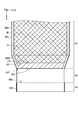
- FIG. 10 is a cross-sectional view showing another example of the display panel 2.
- FIG. 11 is a plan view of the display panel 2 shown in FIG.
- the example shown in FIGS. 10 and 11 is different from the example shown in FIGS. 8 and 9 in that the inorganic layer 171 extends to the third region A3. That is, the end portion EI2 is located in the third region A3.
- the length L1 of the inorganic layer 171 extending to the third region A3 is set so that the strain amount when the third region A3 is bent is 4% or less.
- the inorganic layer 173 is provided over the entire first region A1. That is, in the second direction Y, the position of the end portion EI3 and the position of the end portion EP1 are aligned. Note that the end portion EI3 does not need to exceed the third region A3 toward the second region A2, and may be positioned between the end portion EI1 and the end portion EP1 in the second direction Y.
- the same effect as the example shown in FIGS. 8 and 9 can be obtained.
- both the inorganic layer 171 and the inorganic layer 173 are provided in the whole 1st area
- the inorganic layer 171 is provided in the third region A3, the position of the neutral plane NP in the third region A3 can be brought closer to the wiring WL. Therefore, disconnection of the wiring WL when the third region A3 is bent can be suppressed.
- the organic EL display device having the organic EL element OLED has been described as an example.
- the present embodiment is also applicable to a liquid crystal display device having a liquid crystal layer.
- the display device is a liquid crystal display device, for example, an effect similar to the above effect can be obtained by extending an inorganic insulating layer provided between the pixel electrode and the common electrode to the bent area BA side.
- the present embodiment is applicable to a flexible substrate that includes a functional element such as a sensor but does not include a display element.
- the insulating layer 11 corresponds to the first inorganic insulating layer
- the inorganic layer 171 corresponds to the second inorganic insulating layer
- the inorganic layer 173 corresponds to the third inorganic insulating layer
- the insulating layer Reference numeral 12 corresponds to a fourth inorganic insulating layer.
- the end portion EI1 corresponds to a first end portion
- the end portion EI2 corresponds to a second end portion.
- the end portion EP1 of the support substrate PP1 corresponds to a third end portion.
- the organic layer OL1 corresponds to a first organic insulating layer
- the organic layer OL2 corresponds to a second organic insulating layer
- the organic layer OL3 corresponds to a third organic insulating layer.
Abstract
A display device which is provided with: a substrate (10) which comprises a first area (A1) that has a display area, a second area (A2) that has a mounting area, and a third area (A3) that is positioned between the first area and the second area; a first inorganic insulating layer (11) which is provided on the substrate in the first area and the second area; a wiring line (WL) which is formed on the first inorganic insulating layer so as to extend over the first area, the second area and the third area; and a second inorganic insulating layer (171) which is provided on the wiring line. This display device is configured such that the second inorganic insulating layer extends in an area that overlaps with at least the first inorganic insulating layer.
Description
本発明の実施形態は、表示装置に関する。
Embodiments of the present invention relate to a display device.
携帯電話やPDA(personal digital assistant)等に用いられる表示パネルでは、性能面や、デザイン性等の観点から、表示パネルの一部が折り曲げられる場合がある。配線が配置された領域が折り曲げられた場合、配線への応力が大きくなる。この結果、配線への接触等による衝撃や温度変化などによって配線が断線する場合があり、表示装置の信頼性が低下するおそれがある。
In a display panel used for a mobile phone or a PDA (personal digital assistant), a part of the display panel may be bent from the viewpoint of performance or design. When the region where the wiring is arranged is bent, the stress on the wiring increases. As a result, the wiring may be disconnected due to an impact due to contact with the wiring or a temperature change, and the reliability of the display device may be reduced.
本実施形態の目的は、信頼性の高い表示装置を提供することにある。
The purpose of this embodiment is to provide a display device with high reliability.
本実施形態によれば、表示領域を有する第1領域と、実装領域を有する第2領域と、前記第1領域と前記第2領域との間に位置する第3領域と、を有する基板と、前記第1領域及び前記第2領域において前記基板の上に設けられた第1無機絶縁層と、前記第1無機絶縁層の上に形成され、前記第1領域、前記第2領域、及び前記第3領域に亘って延出した配線と、前記配線の上に設けられた第2無機絶縁層と、を備え、前記第2無機絶縁層は、少なくとも前記第1無機絶縁層と重畳する領域に延在している、表示装置が提供される。
According to the present embodiment, a substrate having a first region having a display region, a second region having a mounting region, and a third region located between the first region and the second region; A first inorganic insulating layer provided on the substrate in the first region and the second region, and formed on the first inorganic insulating layer, the first region, the second region, and the first region A wiring extending over three regions, and a second inorganic insulating layer provided on the wiring, wherein the second inorganic insulating layer extends at least in a region overlapping with the first inorganic insulating layer. A display device is provided.
以下、本実施形態について、図面を参照しながら説明する。なお、開示はあくまで一例に過ぎず、当業者において、発明の主旨を保っての適宜変更について容易に想到し得るものについては、当然に本発明の範囲に含有されるものである。また、図面は、説明をより明確にするため、実際の態様に比べて、各部の幅、厚さ、形状等について模式的に表される場合があるが、あくまで一例であって、本発明の解釈を限定するものではない。また、本明細書と各図において、既出の図に関して前述したものと同一又は類似した機能を発揮する構成要素には同一の参照符号を付し、重複する詳細な説明を適宜省略することがある。
Hereinafter, the present embodiment will be described with reference to the drawings. It should be noted that the disclosure is merely an example, and those skilled in the art can easily conceive of appropriate changes while maintaining the gist of the invention are naturally included in the scope of the present invention. In addition, for the sake of clarity, the drawings may be schematically represented with respect to the width, thickness, shape, etc. of each part as compared to actual aspects, but are merely examples, and The interpretation is not limited. In addition, in the present specification and each drawing, components that perform the same or similar functions as those described above with reference to the previous drawings are denoted by the same reference numerals, and repeated detailed description may be omitted as appropriate. .
図1は、本実施形態に係る表示装置1を概略的に示す平面図である。本実施形態において、表示装置1は、一例として、有機エレクトロルミネッセンス(EL)素子を有する有機EL表示装置である。しかしながら、表示装置1は、液晶層を有する液晶表示装置、あるいは電気泳動型素子等を有する電子ペーパー型表示装置等、他の表示装置であってもよい。
FIG. 1 is a plan view schematically showing the display device 1 according to the present embodiment. In the present embodiment, the display device 1 is an organic EL display device having an organic electroluminescence (EL) element as an example. However, the display device 1 may be another display device such as a liquid crystal display device having a liquid crystal layer or an electronic paper type display device having an electrophoretic element.
図に示す第1方向X、第2方向Y、及び第3方向Zは、互いに直交している。なお、第1方向X、第2方向Y、及び第3方向Zは、90度以外の角度で交差していてもよい。本明細書において、第3方向Zを示す矢印の先端に向かう方向を「上」と定義し、矢印の先端から逆に向かう方向を「下」と定義する。「第1部材の上の第2部材」及び「第1部材の下の第2部材」とした場合、第2部材は、第1部材に接していてもよく、第1部材から離れて位置していてもよい。後者の場合、第1部材と第2部材との間に、第3の部材が介在していてもよい。また、第3方向Zを示す矢印の先端側に表示装置1を観察する観察位置があるものとし、この観察位置から、第1方向X及び第2方向Yで規定されるX-Y平面に向かって見ることを平面視という。
The first direction X, the second direction Y, and the third direction Z shown in the figure are orthogonal to each other. Note that the first direction X, the second direction Y, and the third direction Z may intersect at an angle other than 90 degrees. In this specification, the direction toward the tip of the arrow indicating the third direction Z is defined as “up”, and the direction opposite from the tip of the arrow is defined as “down”. In the case of “the second member above the first member” and “the second member below the first member”, the second member may be in contact with the first member and is located away from the first member. It may be. In the latter case, a third member may be interposed between the first member and the second member. Further, it is assumed that the observation position for observing the display device 1 is on the tip side of the arrow indicating the third direction Z, and from this observation position toward the XY plane defined by the first direction X and the second direction Y. This is called planar view.
表示装置1は、表示パネル2、配線基板3などを備えている。表示パネル2は、第2方向Yに沿った長さが第1方向Xに沿った長さよりも大きい形状を有している。図示した例では、表示パネル2は、第1方向Xに沿った辺EX1及びEX2と、第2方向Yに沿った辺EYを有している。辺EX1及びEX2は、辺EYよりも短い。また、辺EX1は、辺EX2よりも短い。
The display device 1 includes a display panel 2, a wiring board 3, and the like. The display panel 2 has a shape in which the length along the second direction Y is larger than the length along the first direction X. In the illustrated example, the display panel 2 has sides EX1 and EX2 along the first direction X, and a side EY along the second direction Y. Sides EX1 and EX2 are shorter than side EY. Further, the side EX1 is shorter than the side EX2.
表示パネル2は、画像を表示する表示領域DAと、表示領域DAの外側に位置する非表示領域NDAを有している。表示領域DAは、一例では、第2方向Yに沿った一対の長辺と第1方向Xに沿った一対の短辺を有する略長方形状である。表示領域DAは、マトリクス状に配置された複数の画素PXを備えている。後述するように、画素PXは、有機EL素子と、有機EL素子を駆動するためのスイッチング素子などを含んでいる。
The display panel 2 has a display area DA for displaying an image and a non-display area NDA located outside the display area DA. In one example, the display area DA has a substantially rectangular shape having a pair of long sides along the second direction Y and a pair of short sides along the first direction X. The display area DA includes a plurality of pixels PX arranged in a matrix. As will be described later, the pixel PX includes an organic EL element, a switching element for driving the organic EL element, and the like.
また、表示パネル2は、辺EX1の近傍において、端子TEを含む実装領域MTを有している。端子TEと画素PXとは、一対一で、配線WLによって電気的に接続されている。外部装置から供給される電源電位や信号電位は、端子TE及び配線WLを介して、各画素PXに供給される。
Further, the display panel 2 has a mounting region MT including the terminal TE in the vicinity of the side EX1. The terminals TE and the pixels PX are one-to-one and are electrically connected by the wiring WL. The power supply potential and the signal potential supplied from the external device are supplied to each pixel PX via the terminal TE and the wiring WL.
表示パネル2は、可撓性を有している。一例では、表示パネル2は、図において斜線を付して示すように、非表示領域NDAにおいて折り曲げ領域BAを有している。折り曲げ領域BAは、表示装置1が筐体等に収容される際に折り曲げられる領域に相当する。折り曲げ領域BAは、表示領域DAと実装領域MTとの間に位置している。配線WLは、折り曲げ領域BAを通って、画素PXと端子TEとを電気的に接続している。
The display panel 2 has flexibility. In one example, the display panel 2 has a bent area BA in the non-display area NDA, as indicated by hatching in the drawing. The folding area BA corresponds to an area that is bent when the display device 1 is accommodated in a housing or the like. The folding area BA is located between the display area DA and the mounting area MT. The wiring WL electrically connects the pixel PX and the terminal TE through the bent area BA.
配線基板3は、実装領域MTに実装されている。配線基板3は、端子TEを介して、表示パネル2と電気的に接続されている。配線基板3は、例えばフレキシブルプリント回路基板である。図示した例では、配線基板3は、画素PXを駆動するためのICチップ4を搭載している。なお、ICチップ4は、表示パネル2に実装されていてもよい。図示した例では、配線基板3の第1方向Xに沿った辺の長さは、辺EX1と同等であるが、異なっていてもよい。
The wiring board 3 is mounted in the mounting area MT. The wiring board 3 is electrically connected to the display panel 2 via the terminal TE. The wiring board 3 is a flexible printed circuit board, for example. In the illustrated example, the wiring substrate 3 is mounted with an IC chip 4 for driving the pixel PX. Note that the IC chip 4 may be mounted on the display panel 2. In the illustrated example, the length of the side along the first direction X of the wiring board 3 is equal to the side EX1, but may be different.
本実施形態において、表示パネル2は、第1領域A1、第2領域A2、及び第3領域A3を有している。第1領域A1は、表示領域DAを含んでおり、辺EX2と折り曲げ領域BAとの間の領域に相当する。第2領域A2は、実装領域MTを含んでおり、折り曲げ領域BAと辺EX1との間の領域に相当する。第3領域A3は、第1領域A1と第2領域A2領域との間の領域である。図示した例では、第3領域A3は、折り曲げ領域BAに相当する。
In the present embodiment, the display panel 2 has a first area A1, a second area A2, and a third area A3. The first area A1 includes the display area DA and corresponds to an area between the side EX2 and the bent area BA. The second area A2 includes the mounting area MT and corresponds to an area between the bent area BA and the side EX1. The third area A3 is an area between the first area A1 and the second area A2. In the illustrated example, the third area A3 corresponds to the bent area BA.
図2は、図1に示す折り曲げ領域BAが折り曲げられた状態を示す図である。図2は、Y-Z平面に平行な面を示している。ここでは、説明に必要な構成のみを示している。表示装置1は、表示パネル2、配線基板3に加え、支持基板PP(PP1、PP2)、支持部材50、接着剤51などを備えている。
FIG. 2 is a diagram showing a state where the folding area BA shown in FIG. 1 is bent. FIG. 2 shows a plane parallel to the YZ plane. Here, only the configuration necessary for the description is shown. In addition to the display panel 2 and the wiring substrate 3, the display device 1 includes a support substrate PP (PP1, PP2), a support member 50, an adhesive 51, and the like.
支持基板PPは、第3領域A3(すなわち折り曲げ領域BA)を除き、表示パネル2の表示面とは反対側の面に設けられている。第1領域A1は、表示パネル2に支持基板PP1が貼り付けられた領域に相当する。第2領域A2は、表示パネル2に支持基板PP2が貼り付けられた領域に相当する。第3領域A3は、支持基板PPが設けられていない領域、すなわち支持基板PP1と支持基板PP2との間の領域に相当する。
The support substrate PP is provided on the surface opposite to the display surface of the display panel 2 except for the third region A3 (that is, the bent region BA). The first region A1 corresponds to a region where the support substrate PP1 is attached to the display panel 2. The second region A2 corresponds to a region where the support substrate PP2 is attached to the display panel 2. The third region A3 corresponds to a region where the support substrate PP is not provided, that is, a region between the support substrate PP1 and the support substrate PP2.
支持基板PPは、例えば表示領域DA及び実装領域MTにおいて、表示パネル2の湾曲を抑制する支持層として機能する。また、支持基板PPは、表示パネル2への水分等の侵入を抑制する防湿性と、ガスの侵入を抑制するガス遮断性をと有し、バリア層としても機能する。支持基板PPは、一例では、ポリエチレンテレフタラートを用いて形成されたフィルムである。なお、支持基板PPと表示パネル2との間に他の薄膜が介在していてもよい。
The support substrate PP functions as a support layer that suppresses the bending of the display panel 2 in the display area DA and the mounting area MT, for example. Further, the support substrate PP has moisture resistance that suppresses intrusion of moisture and the like into the display panel 2 and gas barrier property that suppresses intrusion of gas, and also functions as a barrier layer. In one example, the support substrate PP is a film formed using polyethylene terephthalate. Note that another thin film may be interposed between the support substrate PP and the display panel 2.
表示パネル2は、支持部材50を挟み込むように折り曲げられ、接着剤51によって支持部材50と貼り付けられている。図示した例では、支持基板PP1及びPP2と接着剤51とが接している。第3領域A3が折り曲げられた状態において、配線基板3は、表示パネル2の下方に位置し、表示パネル2及び支持部材50とほぼ平行に対向している。なお、支持部材50は、省略されてもよい。
The display panel 2 is bent so as to sandwich the support member 50, and is attached to the support member 50 with an adhesive 51. In the illustrated example, the support substrates PP1 and PP2 and the adhesive 51 are in contact with each other. In a state where the third region A3 is bent, the wiring board 3 is located below the display panel 2 and faces the display panel 2 and the support member 50 substantially in parallel. Note that the support member 50 may be omitted.
折り曲げ領域BAは、第1方向Xに沿った折り曲げ軸AXを中心として折り曲げられている。第3領域A3は、曲面状であり、一例では、円周に沿って湾曲している。折り曲げ領域BAが形成する曲面の母線GNは、折り曲げ軸AXと平行である。すなわち、折り曲げ領域BAの母線GNは、第1方向Xと平行である。ここで、折り曲げ領域BAの曲面に沿って第1領域A1側から第2領域A2側へ向かう方向を周方向Cと定義する。また、折り曲げ領域BAの曲率半径R1は、例えば折り曲げ軸AXから表示パネル2の内面までの距離として定義される。一例では、曲率半径R1は、0.3mmである。
The bending area BA is bent around a bending axis AX along the first direction X. The third region A3 has a curved surface shape, and in one example, is curved along the circumference. A curved generatrix GN formed by the folding area BA is parallel to the folding axis AX. That is, the generatrix GN of the bending area BA is parallel to the first direction X. Here, a direction from the first region A1 side to the second region A2 side along the curved surface of the bent region BA is defined as a circumferential direction C. Further, the curvature radius R1 of the bending area BA is defined as a distance from the bending axis AX to the inner surface of the display panel 2, for example. In one example, the radius of curvature R1 is 0.3 mm.
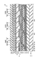
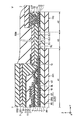
図3は、図1に示す表示領域DAを示す断面図である。表示パネル2は、絶縁基板10、絶縁層11乃至15、リブ16、スイッチング素子SW(SW1、SW2、SW3)、有機EL素子OLED(OLED1、OLED2、OLED3)、封止膜17、粘着層18、光学素子OD1及びOD2などを備えている。図示した例では、支持基板PP1は、絶縁基板10の下に貼り付けられている。
FIG. 3 is a cross-sectional view showing the display area DA shown in FIG. The display panel 2 includes an insulating substrate 10, insulating layers 11 to 15, ribs 16, switching elements SW (SW1, SW2, SW3), organic EL elements OLED (OLED1, OLED2, OLED3), sealing film 17, adhesive layer 18, Optical elements OD1 and OD2 are provided. In the illustrated example, the support substrate PP <b> 1 is pasted under the insulating substrate 10.
絶縁基板10は、例えばポリイミド等の有機絶縁材料によって形成されている。絶縁層11は、絶縁基板10の上に形成されている。絶縁層11は、絶縁基板10から有機EL素子OLEDへの水分等の侵入を抑制するためのバリア層を含んでいてもよい。なお、絶縁層11は、省略されてもよい。また、絶縁基板10は、有機絶縁材料によって挟まれた無機絶縁材料を含む積層構造であってもよい。
The insulating substrate 10 is made of an organic insulating material such as polyimide. The insulating layer 11 is formed on the insulating substrate 10. The insulating layer 11 may include a barrier layer for suppressing entry of moisture or the like from the insulating substrate 10 into the organic EL element OLED. Note that the insulating layer 11 may be omitted. Further, the insulating substrate 10 may have a laminated structure including an inorganic insulating material sandwiched between organic insulating materials.
スイッチング素子SWは、絶縁層11の上に形成されている。スイッチング素子SWは、例えば薄膜トランジスタ(TFT;thin-film-transistor)により構成されている。図示した例では、スイッチング素子SWはトップゲート型であるが、ボトムゲート型であってもよい。以下では、スイッチング素子SW1を例として、その構成を説明する。
The switching element SW is formed on the insulating layer 11. The switching element SW is configured by, for example, a thin film transistor (TFT). In the illustrated example, the switching element SW is a top gate type, but may be a bottom gate type. Hereinafter, the configuration of the switching element SW1 will be described as an example.
スイッチング素子SW1は、半導体層SC、ゲート電極GE、ソース電極SE、及び、ドレイン電極DEを備えている。
The switching element SW1 includes a semiconductor layer SC, a gate electrode GE, a source electrode SE, and a drain electrode DE.
半導体層SCは、絶縁層11の上に形成され、絶縁層12により覆われている。ゲート電極GEは、絶縁層12の上に形成され、絶縁層13により覆われている。ソース電極SE及びドレイン電極DEは、それぞれ絶縁層13の上に形成されている。ソース電極SE及びドレイン電極DEは、絶縁層13及び絶縁層12を半導体層SCまで貫通するコンタクトホールにおいて、半導体層SCにそれぞれ接触している。
The semiconductor layer SC is formed on the insulating layer 11 and covered with the insulating layer 12. The gate electrode GE is formed on the insulating layer 12 and is covered with the insulating layer 13. The source electrode SE and the drain electrode DE are each formed on the insulating layer 13. The source electrode SE and the drain electrode DE are in contact with the semiconductor layer SC in contact holes that penetrate the insulating layer 13 and the insulating layer 12 to the semiconductor layer SC, respectively.
ゲート電極GEは、アルミニウム、チタン、銀、モリブデン、タングステン、銅、クロムなどの金属材料や、これらの金属材料を組み合わせた合金などによって形成され、単層構造であってもよいし、多層構造であってもよい。ソース電極SE及びドレイン電極DEを形成する材料は、上記の金属材料が適用可能である。
The gate electrode GE is formed of a metal material such as aluminum, titanium, silver, molybdenum, tungsten, copper, or chromium, or an alloy that combines these metal materials, and may have a single layer structure or a multilayer structure. There may be. As the material for forming the source electrode SE and the drain electrode DE, the above metal materials can be applied.
各スイッチング素子SWは、絶縁層14により覆われている。絶縁層14は、絶縁層15により覆われている。絶縁層11乃至13、及び絶縁層15は、酸化シリコン、窒化シリコン、酸窒化シリコン等の無機絶縁材料により形成されている。絶縁層14は、例えばポリイミド等の有機絶縁材料により形成されている。
Each switching element SW is covered with an insulating layer 14. The insulating layer 14 is covered with the insulating layer 15. The insulating layers 11 to 13 and the insulating layer 15 are formed of an inorganic insulating material such as silicon oxide, silicon nitride, or silicon oxynitride. The insulating layer 14 is made of an organic insulating material such as polyimide, for example.
有機EL素子OLEDは、絶縁層15の上に形成されている。図示した例では、有機EL素子OLEDは、絶縁基板10とは反対側に光を出射する所謂トップエミッションタイプであるが、この例に限らず、絶縁基板10の側に光を出射する所謂ボトムエミッションタイプであってもよい。一例では、有機EL素子OLED1は、赤色に発光する有機発光層ORG1を備え、有機EL素子OLED2は、青色に発光する有機発光層ORG2を備え、有機EL素子OLED3は、緑色に発光する有機発光層ORG3を備えている。以下では、有機EL素子OLED1を例として、その構成を説明する。
The organic EL element OLED is formed on the insulating layer 15. In the illustrated example, the organic EL element OLED is a so-called top emission type that emits light to the side opposite to the insulating substrate 10, but is not limited to this example, and so-called bottom emission that emits light to the insulating substrate 10 side. It may be a type. In one example, the organic EL element OLED1 includes an organic light emitting layer ORG1 that emits red light, the organic EL element OLED2 includes an organic light emitting layer ORG2 that emits blue light, and the organic EL element OLED3 emits an green light emitting layer. ORG3 is provided. Below, the structure is demonstrated taking the organic EL element OLED1 as an example.
有機EL素子OLED1は、画素電極PE1、共通電極CE、及び有機発光層ORG1により構成されている。画素電極PE1は、絶縁層15の上に設けられている。画素電極PE1は、絶縁層15及び14に設けられたコンタクトホールにおいて、スイッチング素子SW1のドレイン電極DEと接触している。これにより、画素電極PE1とスイッチング素子SW1とは、互いに電気的に接続される。有機発光層ORG1は、画素電極PE1の上に形成されている。有機発光層ORG1は、発光効率を向上するために、電子注入層、正孔注入層、電子輸送層、正孔輸送層等をさらに含んでいてもよい。共通電極CEは、有機発光層ORG1の上に形成されている。共通電極CEと画素電極PEとは、例えばインジウム・ティン・オキサイド(ITO)やインジウム・ジンク・オキサイド(IZO)等の透明な導電材料によって形成されている。
The organic EL element OLED1 includes a pixel electrode PE1, a common electrode CE, and an organic light emitting layer ORG1. The pixel electrode PE1 is provided on the insulating layer 15. The pixel electrode PE1 is in contact with the drain electrode DE of the switching element SW1 in a contact hole provided in the insulating layers 15 and 14. Thereby, the pixel electrode PE1 and the switching element SW1 are electrically connected to each other. The organic light emitting layer ORG1 is formed on the pixel electrode PE1. The organic light emitting layer ORG1 may further include an electron injection layer, a hole injection layer, an electron transport layer, a hole transport layer, and the like in order to improve the light emission efficiency. The common electrode CE is formed on the organic light emitting layer ORG1. The common electrode CE and the pixel electrode PE are formed of a transparent conductive material such as indium tin oxide (ITO) or indium zinc oxide (IZO).
以上のように構成された有機EL素子OLED1は、画素電極PE1と共通電極CEとの間に印加される電圧(あるいは電流)に応じた輝度で発光する。なお、図示は省略するが、トップエミッションタイプの場合には、有機EL素子OLED1は、絶縁層15と画素電極PE1との間に反射層を含んでいることが望ましい。反射層は、例えばアルミニウム、銀等の反射率の高い金属材料により形成される。なお、反射層の反射面、すなわち有機発光層ORG1側の面は、平坦であってもよいし、光散乱性を付与するために凹凸が形成されていてもよい。
The organic EL element OLED1 configured as described above emits light with luminance according to a voltage (or current) applied between the pixel electrode PE1 and the common electrode CE. Although illustration is omitted, in the case of the top emission type, it is desirable that the organic EL element OLED1 includes a reflective layer between the insulating layer 15 and the pixel electrode PE1. The reflective layer is formed of a metal material having high reflectivity such as aluminum or silver. In addition, the reflective surface of the reflective layer, that is, the surface on the organic light emitting layer ORG1 side may be flat, or irregularities may be formed to impart light scattering properties.
各有機EL素子OLEDは、有機絶縁材料からなるリブ16により、画素PXごとに区画されている。リブ16は、各画素電極PEの両端部を覆うとともに、絶縁層15とも接している。リブ16は、例えばポリイミドによって形成されている。有機発光層ORG1、ORG2、及びORG3は、リブ16が設けられていない領域において、画素電極PE1、PE2、及びPE3とそれぞれ接している。共通電極CEは、表示領域DAの全体に亘って形成されている。すなわち、共通電極CEは、有機発光層ORG1、ORG2、及びORG3と接するとともに、リブ16を覆っている。
Each organic EL element OLED is partitioned for each pixel PX by a rib 16 made of an organic insulating material. The rib 16 covers both ends of each pixel electrode PE and is in contact with the insulating layer 15. The rib 16 is made of polyimide, for example. The organic light emitting layers ORG1, ORG2, and ORG3 are in contact with the pixel electrodes PE1, PE2, and PE3, respectively, in regions where the ribs 16 are not provided. The common electrode CE is formed over the entire display area DA. That is, the common electrode CE is in contact with the organic light emitting layers ORG1, ORG2, and ORG3 and covers the ribs 16.
なお、表示パネル2は、複数の画素PXに亘って共通の有機発光層を有していてもよい。このような構成においては、表示パネル2は、各有機EL素子OLEDと対向する位置にカラーフィルタを備える。カラーフィルタは、例えば赤色、緑色、青色等に着色された樹脂材料によって形成される。
In addition, the display panel 2 may have a common organic light emitting layer over the plurality of pixels PX. In such a configuration, the display panel 2 includes a color filter at a position facing each organic EL element OLED. The color filter is formed of a resin material colored in red, green, blue, or the like, for example.
封止膜17は、有機EL素子OLEDを覆っている。封止膜17は、有機EL素子OLEDへの水分や酸素の侵入を抑制し、有機EL素子OLEDの劣化を抑制する。封止膜17は、無機層171、有機層172、及び無機層173を備えている。無機層171は、有機EL素子OLEDの上に形成されている。図示した例では、無機層171は、共通電極CEと接している。無機層173は、無機層171の上方に位置している。有機層172は、無機層171と無機層173の間に位置し、無機層171及び無機層173の双方と接している。
The sealing film 17 covers the organic EL element OLED. The sealing film 17 suppresses intrusion of moisture and oxygen into the organic EL element OLED, and suppresses deterioration of the organic EL element OLED. The sealing film 17 includes an inorganic layer 171, an organic layer 172, and an inorganic layer 173. The inorganic layer 171 is formed on the organic EL element OLED. In the illustrated example, the inorganic layer 171 is in contact with the common electrode CE. The inorganic layer 173 is located above the inorganic layer 171. The organic layer 172 is located between the inorganic layer 171 and the inorganic layer 173 and is in contact with both the inorganic layer 171 and the inorganic layer 173.
封止膜17のうち、無機層171及び無機層173は、主に、有機EL素子OLED側への水分の侵入を遮断する機能を有している。無機層171及び無機層173は、透明であり、例えば酸化シリコン、窒化シリコン、又は酸窒化シリコン等の無機絶縁材料によって形成されている。無機層171と無機層173とは、同一の材料で形成されてもよく、異なる材料で形成されてもよい。有機層172は、透明な有機絶縁材料によって形成されている。なお、ここでの透明とは、透過光が表示に影響のない範囲で着色されることを許容するものである。
Of the sealing film 17, the inorganic layer 171 and the inorganic layer 173 mainly have a function of blocking moisture from entering the organic EL element OLED. The inorganic layer 171 and the inorganic layer 173 are transparent, and are formed of an inorganic insulating material such as silicon oxide, silicon nitride, or silicon oxynitride. The inorganic layer 171 and the inorganic layer 173 may be formed of the same material or different materials. The organic layer 172 is formed of a transparent organic insulating material. Here, the term “transparent” means that the transmitted light is allowed to be colored within a range that does not affect the display.
光学素子OD1及びOD2は、封止膜17の上に設けられている。光学素子OD1は、一例では、位相差板等の光学部材である。光学素子OD2は、一例では、偏光板等の光学部材である。図示した例では、光学素子OD1は、光学素子OD2よりも封止膜17に近接し、粘着層18によって封止膜17に接着されている。
The optical elements OD1 and OD2 are provided on the sealing film 17. In one example, the optical element OD1 is an optical member such as a retardation plate. For example, the optical element OD2 is an optical member such as a polarizing plate. In the illustrated example, the optical element OD1 is closer to the sealing film 17 than the optical element OD2, and is bonded to the sealing film 17 by the adhesive layer 18.
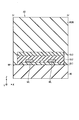
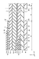
図4は、図1に示すIV-IV’線に沿った断面図である。図4は、第1方向X及び第3方向Zによって規定されるX-Z平面と平行な面を示している。第3領域A3において、表示パネル2は、絶縁基板10、及び配線WLに加え、有機層OL1、OL2及びOL3、及び樹脂層RSNを備えている。
FIG. 4 is a cross-sectional view taken along line IV-IV ′ shown in FIG. FIG. 4 shows a plane parallel to the XZ plane defined by the first direction X and the third direction Z. In the third region A3, the display panel 2 includes organic layers OL1, OL2, OL3, and a resin layer RSN in addition to the insulating substrate 10 and the wiring WL.
有機層OL1は、絶縁基板10の上に位置している。配線WLは、有機層OL1の上に位置し、有機層OL2によって覆われている。図示した例では、第1方向Xにおいて、有機層OL1の両端部は、有機層OL2によって覆われている。すなわち、有機層OL2は、配線WL及び有機層OL1と接するとともに、有機層OL1を挟んだ両側で絶縁基板10とも接している。有機層OL3は、有機層OL2の上に設けられている。樹脂層RSNは、有機層OL3の上に設けられている。図示した例では、樹脂層RSNは、有機層OL1、OL2及びOL3を挟んだ両側で、絶縁基板10と接している。
The organic layer OL1 is located on the insulating substrate 10. The wiring WL is located on the organic layer OL1 and is covered with the organic layer OL2. In the illustrated example, in the first direction X, both ends of the organic layer OL1 are covered with the organic layer OL2. That is, the organic layer OL2 is in contact with the wiring WL and the organic layer OL1, and is also in contact with the insulating substrate 10 on both sides of the organic layer OL1. The organic layer OL3 is provided on the organic layer OL2. The resin layer RSN is provided on the organic layer OL3. In the illustrated example, the resin layer RSN is in contact with the insulating substrate 10 on both sides of the organic layers OL1, OL2, and OL3.
有機層OL1、OL2、及びOL3は、例えばポリイミド等の有機絶縁材料によって形成されている。密着性を向上するために、有機層OL1と有機層OL2とは、同一材料で形成されることが望ましい。また、ポリイミドによって形成される場合、有機層OL1、OL2、及びOL3のうち、少なくとも有機層OL1及びOL2は、フッ素を含んでいることが望ましい。有機層OL3は、フッ素を含んでいてもよく、含んでいなくてもよい。有機層OL1及びOL2がフッ素を含む場合、これらの透湿性及び吸湿性が低下するため、有機層OL1と有機層OL2との間に配置された配線WLの腐食を抑制することができる。樹脂層RSNは、一例では、アクリル系の樹脂であり、紫外線の照射によって硬化される。このような樹脂層RSNは、配線WLを保護する保護層として機能する。
The organic layers OL1, OL2, and OL3 are formed of an organic insulating material such as polyimide, for example. In order to improve adhesion, the organic layer OL1 and the organic layer OL2 are desirably formed of the same material. Moreover, when formed with polyimide, it is desirable that at least the organic layers OL1 and OL2 among the organic layers OL1, OL2, and OL3 contain fluorine. The organic layer OL3 may or may not contain fluorine. When the organic layers OL1 and OL2 contain fluorine, their moisture permeability and hygroscopicity are lowered, so that the corrosion of the wiring WL disposed between the organic layer OL1 and the organic layer OL2 can be suppressed. In one example, the resin layer RSN is an acrylic resin and is cured by irradiation with ultraviolet rays. Such a resin layer RSN functions as a protective layer for protecting the wiring WL.
有機層OL1、OL2、及びOL3のヤング率は、いずれも樹脂層RSNのヤング率より大きい。上記の構成において、折り曲げ領域BAが折り曲げられた際の中立面NPは、図において破線で示すように、絶縁基板10と有機層OL1との境界近傍に位置している。ここで、中立面NPとは、折り曲げ領域BAが折り曲げられた際の引っ張り応力と圧縮応力とがつり合う面である。
The Young's modulus of the organic layers OL1, OL2, and OL3 are all greater than the Young's modulus of the resin layer RSN. In the above configuration, the neutral plane NP when the bent area BA is bent is located in the vicinity of the boundary between the insulating substrate 10 and the organic layer OL1, as indicated by a broken line in the drawing. Here, the neutral surface NP is a surface where the tensile stress and the compressive stress are balanced when the folding area BA is bent.
図5は、図1に示すV-V’線に沿った断面図である。図5は、Y-Z平面と平行な面を示している。第1領域A1、第3領域A3、及び第2領域A2は、この順で第2方向Yに沿って並んでいる。第1領域A1に設けられる支持基板PP1は、有機EL素子OLEDと重なる支持基板PPである。第2領域A2に設けられる支持基板PP2は、端子TEと重なる支持基板PPである。なお、第3領域A3が折り曲げられている場合は、第2方向Yは、図2に示す周方向Cに相当する。
FIG. 5 is a cross-sectional view taken along the line V-V ′ shown in FIG. FIG. 5 shows a plane parallel to the YZ plane. The first region A1, the third region A3, and the second region A2 are arranged along the second direction Y in this order. The support substrate PP1 provided in the first region A1 is a support substrate PP that overlaps with the organic EL element OLED. The support substrate PP2 provided in the second region A2 is a support substrate PP that overlaps the terminal TE. When the third region A3 is bent, the second direction Y corresponds to the circumferential direction C shown in FIG.
表示パネル2は、絶縁基板10、絶縁層11乃至15、リブ16、有機EL素子OLED、封止膜17、粘着層18、光学素子OD1及びOD2、配線WL、有機層OL1、OL2、及びOL3、及び端子TEに加え、配線GL及び導電層CLを備えている。
The display panel 2 includes an insulating substrate 10, insulating layers 11 to 15, ribs 16, organic EL elements OLED, sealing film 17, adhesive layer 18, optical elements OD1 and OD2, wiring WL, organic layers OL1, OL2, and OL3, In addition to the terminal TE, the wiring GL and the conductive layer CL are provided.
絶縁基板10は、第1領域A1、第2領域A2、及び第3領域A3に亘って設けられている。絶縁層11乃至13は、第1領域A1及び第2領域A2に設けられているが、第3領域A3には設けられていない。図示した例では、絶縁層11乃至13は、第3領域A3よりも若干広い領域において除去されている。換言すると、絶縁層11乃至13は、第1領域A1の第3領域A3側の端部、及び第2領域A2の第3領域A3側の端部には設けられていない。第1領域A1において、絶縁層11は、絶縁層12及び13よりも第2領域A2側に延出している。また、第2領域A2において、絶縁層11は、絶縁層12及び13よりも第1領域A1側に延出している。
The insulating substrate 10 is provided over the first region A1, the second region A2, and the third region A3. The insulating layers 11 to 13 are provided in the first region A1 and the second region A2, but are not provided in the third region A3. In the illustrated example, the insulating layers 11 to 13 are removed in a region slightly wider than the third region A3. In other words, the insulating layers 11 to 13 are not provided at the end of the first region A1 on the third region A3 side and the end of the second region A2 on the third region A3 side. In the first region A1, the insulating layer 11 extends further to the second region A2 side than the insulating layers 12 and 13. In the second region A2, the insulating layer 11 extends further to the first region A1 side than the insulating layers 12 and 13.
配線GLは、第1領域A1において、絶縁層12の上に位置し、絶縁層13によって覆われている。配線GLは、図3に示すスイッチング素子SWのゲート電極GEと電気的に接続されている。このような配線GLは、例えば、図3に示すスイッチング素子SWのゲート電極GEと同一材料及び同一工程で形成することができる。
The wiring GL is located on the insulating layer 12 and covered with the insulating layer 13 in the first region A1. The wiring GL is electrically connected to the gate electrode GE of the switching element SW shown in FIG. Such a wiring GL can be formed with the same material and the same process as the gate electrode GE of the switching element SW shown in FIG. 3, for example.
配線WLは、第1領域A1の第3領域A3側の端部から第2領域A2まで延出している。配線WLは、第1領域A1及び第2領域A2において、絶縁層13の上に形成され、第3領域A3において有機層OL1の上に形成されている。第1領域A1において、配線WLは、絶縁層13に形成されたコンタクトホールにおいて、配線GLと接している。これにより、配線WLと配線GLとは、電気的に接続される。配線WLは、例えば、図3に示すスイッチング素子SWのソース電極SE及びドレイン電極DEと同一材料及び同一工程で形成することができる。
The wiring WL extends from the end of the first region A1 on the third region A3 side to the second region A2. The wiring WL is formed on the insulating layer 13 in the first region A1 and the second region A2, and is formed on the organic layer OL1 in the third region A3. In the first region A1, the wiring WL is in contact with the wiring GL in the contact hole formed in the insulating layer 13. Thereby, the wiring WL and the wiring GL are electrically connected. For example, the wiring WL can be formed using the same material and the same process as the source electrode SE and the drain electrode DE of the switching element SW shown in FIG.
有機層OL1は、少なくとも第3領域A3に設けられている。図示した例では、有機層OL1の第2方向Yにおける両端部は、第1領域A1及び第2領域A2に位置している。有機層OL1は、第3領域A3において、絶縁基板10の上に形成されている。また、有機層OL1は、第1領域A1及び第2領域A2において、絶縁基板10の上に形成されるとともに、絶縁層11乃至13の一部を覆っている。このように、第1領域A1及び第2領域A2において有機層OL1が絶縁層11乃至13の一部を覆うことにより、絶縁層11乃至13の端部近傍に形成される段差が緩和される。したがって、第1領域A1及び第2領域A2において、絶縁層13の上、及び有機層OL1の上に形成される配線WLの断線を抑制することができる。
The organic layer OL1 is provided at least in the third region A3. In the illustrated example, both end portions in the second direction Y of the organic layer OL1 are located in the first region A1 and the second region A2. The organic layer OL1 is formed on the insulating substrate 10 in the third region A3. In addition, the organic layer OL1 is formed on the insulating substrate 10 and covers a part of the insulating layers 11 to 13 in the first region A1 and the second region A2. As described above, the organic layer OL1 covers a part of the insulating layers 11 to 13 in the first region A1 and the second region A2, so that the step formed in the vicinity of the end portions of the insulating layers 11 to 13 is alleviated. Therefore, in the first region A1 and the second region A2, disconnection of the wiring WL formed on the insulating layer 13 and the organic layer OL1 can be suppressed.
有機層OL2は、第1領域A1、第2領域A2、及び第3領域A3に亘って設けられ、配線WLを覆っている。図示した例では、有機層OL2は、第1領域A1及び第2領域A2において配線WLを覆うとともに、絶縁層13とも接している。有機層OL2は、例えば絶縁層14と同一材料及び同一工程で形成することができる。有機層OL2は、第2領域A2において、配線WLを露出するコンタクトホールを有している。導電層CLは、このコンタクトホール内に設けられ、配線WLと接している。導電層CLは、例えば画素電極PEと同一材料及び同一工程で形成することができる。
The organic layer OL2 is provided over the first region A1, the second region A2, and the third region A3, and covers the wiring WL. In the illustrated example, the organic layer OL2 covers the wiring WL in the first region A1 and the second region A2, and is in contact with the insulating layer 13 as well. The organic layer OL2 can be formed by the same material and the same process as the insulating layer 14, for example. The organic layer OL2 has a contact hole that exposes the wiring WL in the second region A2. The conductive layer CL is provided in the contact hole and is in contact with the wiring WL. The conductive layer CL can be formed, for example, with the same material and the same process as the pixel electrode PE.
有機層OL3は、有機層OL2と重畳する領域に設けられている。すなわち、有機層OL3は、第1領域A1、第2領域A2、及び第3領域A3に亘って設けられている。有機層OL3は、例えばリブ16と同一材料及び同一工程で形成することができる。有機層OL3は、第2領域A2において、導電層CLを露出するコンタクトホールを有している。端子TEは、このコンタクトホール内に設けられ、導電層CLと接している。これにより、端子TEと配線WLとは、導電層CLを介して電気的に接続される。端子TEは、例えば共通電極CEと同時に形成することができる。図示した例では、端子TEは、異方性導電膜ACFを介して、配線基板3と電気的に接続されている。
The organic layer OL3 is provided in a region overlapping with the organic layer OL2. That is, the organic layer OL3 is provided over the first region A1, the second region A2, and the third region A3. The organic layer OL3 can be formed by the same material and the same process as the rib 16, for example. The organic layer OL3 has a contact hole that exposes the conductive layer CL in the second region A2. The terminal TE is provided in the contact hole and is in contact with the conductive layer CL. Thereby, the terminal TE and the wiring WL are electrically connected via the conductive layer CL. The terminal TE can be formed at the same time as the common electrode CE, for example. In the illustrated example, the terminal TE is electrically connected to the wiring board 3 via the anisotropic conductive film ACF.
絶縁層14は、第1領域A1内に設けられ、配線WLよりも第2領域A2から離間する側に位置している。絶縁層14は、一例では、絶縁層13を露出する溝14Tを有している。溝14Tが設けられることにより、第2領域A2側から第1領域A1側への絶縁層14を介した水分の浸入が抑制され、有機EL素子OLEDの劣化が抑制される。また、第3領域A3を折り曲げた際に、後述する無機層171及び173などにクラックが生じた場合であっても、溝14Tやこれに起因した凹凸が形成されていることで、クラックの表示領域DA側への伝搬を抑制することができる。このような溝14Tは、平面視で表示領域DAを囲む環状に形成されていることが望ましい。
The insulating layer 14 is provided in the first region A1, and is located on the side farther from the second region A2 than the wiring WL. For example, the insulating layer 14 has a groove 14 </ b> T that exposes the insulating layer 13. By providing the groove 14T, moisture permeation through the insulating layer 14 from the second region A2 side to the first region A1 side is suppressed, and deterioration of the organic EL element OLED is suppressed. Further, even when a crack is generated in the inorganic layers 171 and 173, which will be described later, when the third region A3 is bent, the display of the crack is caused by the formation of the groove 14T and the unevenness resulting therefrom. Propagation to the area DA side can be suppressed. Such a groove 14T is preferably formed in an annular shape surrounding the display area DA in plan view.
絶縁層15は、第1領域A1内に設けられ、絶縁層14の全体を覆っている。すなわち、絶縁層15は、溝14Tにおいて、絶縁層13と接するとともに、絶縁層14よりも第2領域A2側に延出し、絶縁層13と接している。有機EL素子OLED及びリブ16は、溝14Tよりも内側の領域、すなわち溝14Tよりも第2領域A2から離間した側(もしくは表示領域DA側)に位置している。
The insulating layer 15 is provided in the first region A1 and covers the entire insulating layer 14. That is, the insulating layer 15 is in contact with the insulating layer 13 in the groove 14T, extends to the second region A2 side from the insulating layer 14, and is in contact with the insulating layer 13. The organic EL element OLED and the rib 16 are located in a region inside the groove 14T, that is, a side farther from the second region A2 than the groove 14T (or the display region DA side).
封止膜17は、第1領域A1内に設けられ、その一部が絶縁層14よりも第2領域A2側に延出している。より具体的には、封止膜17のうち無機層171は、絶縁層14よりも第2領域A2側に延出し、有機層OL2及びOL3と接している。図示した例では、無機層171は、有機層OL2及びOL3の側面を覆うとともに、有機層OL3の上まで延在している。封止膜17のうち有機層172は、絶縁層14と重畳する領域内に設けられている。封止膜17のうち無機層173は、有機層172よりも第2領域A2側に延出し、無機層171と接している。
The sealing film 17 is provided in the first region A1, and a part thereof extends to the second region A2 side with respect to the insulating layer 14. More specifically, the inorganic layer 171 in the sealing film 17 extends to the second region A2 side with respect to the insulating layer 14, and is in contact with the organic layers OL2 and OL3. In the illustrated example, the inorganic layer 171 covers the side surfaces of the organic layers OL2 and OL3 and extends to above the organic layer OL3. The organic layer 172 of the sealing film 17 is provided in a region overlapping with the insulating layer 14. Of the sealing film 17, the inorganic layer 173 extends toward the second region A <b> 2 with respect to the organic layer 172, and is in contact with the inorganic layer 171.
本実施形態において、無機層171及び173は、少なくとも、配線WLより下方に位置する無機層、すなわち絶縁層11乃至13と重畳する領域に延在している。一例では、無機層171及び173の双方は、絶縁層11乃至13よりも第2領域A2側に延在している。
In the present embodiment, the inorganic layers 171 and 173 extend at least in a region overlapping with the inorganic layers located below the wiring WL, that is, the insulating layers 11 to 13. In one example, both of the inorganic layers 171 and 173 extend to the second region A2 side with respect to the insulating layers 11 to 13.
図示した例では、絶縁層11乃至13と無機層171及び173とは、光学素子OD1及びOD2と重なるとともに、光学素子OD1及びOD2よりも第2領域A2側に延出している。また、配線WL、及び有機層OL2及びOL3は、光学素子OD1及びOD2よりも第2領域A2側の領域に配置されている。図示した例では、配線WLは、光学素子OD1及びOD2と重畳していないが、有機層OL2及びOL3の有機EL素子OLED側の端部は、光学素子OD1及びOD2と重畳している。光学素子OD1及びOD2よりも第2領域A2側の領域において、配線WLと有機層OL2及びOL3とは、絶縁層11乃至13と、無機層171及び173とによって挟まれている。
In the illustrated example, the insulating layers 11 to 13 and the inorganic layers 171 and 173 overlap the optical elements OD1 and OD2, and extend to the second region A2 side from the optical elements OD1 and OD2. Further, the wiring WL and the organic layers OL2 and OL3 are arranged in a region closer to the second region A2 than the optical elements OD1 and OD2. In the illustrated example, the wiring WL does not overlap with the optical elements OD1 and OD2, but the ends of the organic layers OL2 and OL3 on the organic EL element OLED side overlap with the optical elements OD1 and OD2. In the region closer to the second region A2 than the optical elements OD1 and OD2, the wiring WL and the organic layers OL2 and OL3 are sandwiched between the insulating layers 11 to 13 and the inorganic layers 171 and 173.
樹脂層RSNは、第1領域A1、第2領域A2、及び第3領域A3に亘って設けられている。第1領域A1において、樹脂層RSNは、有機層OL3と無機層171及び173とを覆うとともに、粘着層18、及び光学素子OD1及びOD2とも接している。第2領域A2において、樹脂層RSNは、有機層OL3及び配線基板3を覆っている。第3領域A3において、樹脂層RSNは、有機層OL3を覆っている。
The resin layer RSN is provided over the first region A1, the second region A2, and the third region A3. In the first region A1, the resin layer RSN covers the organic layer OL3 and the inorganic layers 171 and 173, and is in contact with the adhesive layer 18 and the optical elements OD1 and OD2. In the second region A2, the resin layer RSN covers the organic layer OL3 and the wiring board 3. In the third region A3, the resin layer RSN covers the organic layer OL3.
なお、有機層OL1、OL2、及びOL3と樹脂層RSNのうち、少なくとも有機層OL1と樹脂層RSNとに、架橋剤が添加されていてもよい。一般に、表示パネルは、配線等の各種導電層や、各種絶縁層を含む多層構造となっている。このため、表示パネルが曲率を有するように変形される折り曲げ領域では、層と層の間の密着性が弱い場合に、折り曲げによる層と層との剥離や、剥離に伴う亀裂が発生する場合がある。特に、折り曲げの開始点(本実施形態においては、第1領域A1と第3領域A3との境界近傍)には折り曲げによる応力が加わりやすいため、層の剥離が生じやすい。このような剥離部分は、表示パネルへの水分の浸入経路となり得る。
In addition, a crosslinking agent may be added to at least the organic layer OL1 and the resin layer RSN among the organic layers OL1, OL2, and OL3 and the resin layer RSN. In general, the display panel has a multilayer structure including various conductive layers such as wiring and various insulating layers. For this reason, in the bent region where the display panel is deformed to have a curvature, if the adhesion between the layers is weak, peeling between the layers due to bending or a crack accompanying the peeling may occur. is there. Particularly, since stress due to bending is likely to be applied to the starting point of bending (in the present embodiment, in the vicinity of the boundary between the first region A1 and the third region A3), layer peeling is likely to occur. Such a peeled portion can be a moisture intrusion path into the display panel.
一方、本実施形態において、有機層OL1に架橋剤が含まれる場合、有機層OL1と絶縁基板10との密着性が向上する。また、樹脂層RSNに架橋剤が含まれる場合、樹脂層RSNと有機層OL3との密着性が向上する。この結果、第3領域A3が折り曲げられた場合であっても、有機層OL1と絶縁基板10との剥離、及び樹脂層RSNと有機層OL3との剥離を抑制することができる。また、樹脂層RSNに架橋剤が含まれる場合、第1領域A1においては、樹脂層RSNと、光学素子OD1及びOD2、粘着層18、及び無機層171及び173との間の密着性も向上する。したがって、第1領域A1における折り曲げ開始点の近傍において、樹脂層RSNの剥離を抑制することができる。この結果、表示装置1の信頼性の低下を抑制することができる。
On the other hand, in this embodiment, when the organic layer OL1 contains a crosslinking agent, the adhesion between the organic layer OL1 and the insulating substrate 10 is improved. Moreover, when the crosslinking agent is contained in the resin layer RSN, the adhesion between the resin layer RSN and the organic layer OL3 is improved. As a result, even when the third region A3 is bent, peeling between the organic layer OL1 and the insulating substrate 10 and peeling between the resin layer RSN and the organic layer OL3 can be suppressed. Further, when the resin layer RSN contains a cross-linking agent, the adhesion between the resin layer RSN and the optical elements OD1 and OD2, the adhesive layer 18, and the inorganic layers 171 and 173 is also improved in the first region A1. . Therefore, peeling of the resin layer RSN can be suppressed in the vicinity of the bending start point in the first region A1. As a result, a decrease in reliability of the display device 1 can be suppressed.
図6は、図5に示す第3領域A3の近傍を拡大して示す断面図である。支持基板PP1は、第2領域A2側の端部EP1を有している。支持基板PP2は、第1領域A1側の端部EP2を有している。第3領域A3は、端部EP1と端部EP2との間の領域に相当する。
FIG. 6 is an enlarged sectional view showing the vicinity of the third region A3 shown in FIG. The support substrate PP1 has an end EP1 on the second region A2 side. The support substrate PP2 has an end portion EP2 on the first region A1 side. The third region A3 corresponds to a region between the end portion EP1 and the end portion EP2.
図示した例では、無機層171の端部EI2、及び無機層173の端部EI3の双方は、絶縁層11の端部EI1、及び絶縁層12及び13の端部EI4の双方よりも第2領域A2に近接している。換言すると、端部EI1及びEI4は、いずれも無機層171及び173と重畳している。ここで、端部EI1、EI2、EI3及びEI4は、第2領域A2側の端部である。端部EI1、EI2、EI3及びEI4は、第1領域A1に位置している。すなわち、端部EI1、EI2、EI3、及びEI4は、端部EP1よりも第2領域A2から離間している。
In the illustrated example, both the end portion EI2 of the inorganic layer 171 and the end portion EI3 of the inorganic layer 173 are in the second region than both the end portion EI1 of the insulating layer 11 and the end portions EI4 of the insulating layers 12 and 13. Close to A2. In other words, both the end portions EI1 and EI4 overlap with the inorganic layers 171 and 173. Here, the end portions EI1, EI2, EI3, and EI4 are end portions on the second region A2 side. The end portions EI1, EI2, EI3, and EI4 are located in the first region A1. That is, the end portions EI1, EI2, EI3, and EI4 are further away from the second region A2 than the end portion EP1.
図示した例では、第2方向Yにおいて、端部EI2の位置と端部EI3の位置とは、揃っている。なお、第2方向Yにおいて、端部EI2の位置と端部EI3の位置とは、端部EI1の位置と揃っていてもよい。また、図示した例では、端部EI1は、端部EI4よりも第2領域A2に近接している。図示した例では、絶縁層12の端部と絶縁層13の端部とは揃っているが、揃っていなくてもよい。この場合、絶縁層12の端部は、絶縁層13の端部よりも第2領域A2に近接する。
In the illustrated example, the position of the end EI2 and the position of the end EI3 are aligned in the second direction Y. In the second direction Y, the position of the end portion EI2 and the position of the end portion EI3 may be aligned with the position of the end portion EI1. In the illustrated example, the end portion EI1 is closer to the second region A2 than the end portion EI4. In the illustrated example, the end of the insulating layer 12 and the end of the insulating layer 13 are aligned, but may not be aligned. In this case, the end portion of the insulating layer 12 is closer to the second region A2 than the end portion of the insulating layer 13.
なお、絶縁層11乃至13は、酸化シリコンで形成されることが望ましい。酸化シリコンは、窒化シリコンよりも引っ張り応力が大きいため、第3領域A3が折り曲げられた際のクラックの発生を抑制することができる。
Note that the insulating layers 11 to 13 are preferably formed of silicon oxide. Since silicon oxide has a larger tensile stress than silicon nitride, generation of cracks when the third region A3 is bent can be suppressed.
図7は、絶縁層11及び無機層171が設けられた領域を示す平面図である。図において右下がりの斜線を付して示すように、絶縁層11は、第1領域A1のほぼ全体に設けられている。また、図において右上がりの斜線を付して示すように、無機層171は、少なくとも絶縁層11と重畳する領域に設けられ、本実施形態では、絶縁層11よりも第2領域A2側に延出している。すなわち、端部EI2は、端部EI1よりも第2領域A2に近接している。端部EI1及びEI2は、一例では、第1方向Xに沿って延出している。
FIG. 7 is a plan view showing a region where the insulating layer 11 and the inorganic layer 171 are provided. As shown with a slanting line with a downward slant in the figure, the insulating layer 11 is provided over substantially the entire first region A1. In addition, as shown by a diagonal line rising to the right in the drawing, the inorganic layer 171 is provided at least in a region overlapping with the insulating layer 11, and in this embodiment, extends to the second region A2 side from the insulating layer 11. I'm out. That is, the end portion EI2 is closer to the second region A2 than the end portion EI1. The end portions EI1 and EI2 extend along the first direction X in one example.
図示した例では、支持基板PPは、第3領域A3を除き、絶縁基板10とほぼ重畳している。すなわち、支持基板PP1の形状は、第1領域A1の形状とほぼ等しく、支持基板PP2の形状は、第2領域A2の形状とほぼ等しい。支持基板PP1の端部EP1と支持基板PP2の端部EP2は、一例では、第1方向Xに沿って延出している。端部EI1及びEI2は、光学素子OD2の端部EODと支持基板PP1の端部EP1との間に位置している。
In the illustrated example, the support substrate PP substantially overlaps the insulating substrate 10 except for the third region A3. That is, the shape of the support substrate PP1 is substantially equal to the shape of the first region A1, and the shape of the support substrate PP2 is substantially equal to the shape of the second region A2. In one example, the end portion EP1 of the support substrate PP1 and the end portion EP2 of the support substrate PP2 extend along the first direction X. The end portions EI1 and EI2 are located between the end portion EOD of the optical element OD2 and the end portion EP1 of the support substrate PP1.
以上のように、本実施形態によれば、第1領域A1において、無機層171及び173は、少なくとも、絶縁層11乃至13が設けられた領域に延在している。一般に、無機層の弾性率は、有機層の弾性率よりも高い。したがって、第1領域A1において、無機層からなる絶縁層11乃至13と無機層171及び173とを積層することにより、第1領域A1の剛性を高めることができる。一方、第3領域A3には、絶縁層11乃至13、及び無機層171及び173は、設けられてない。このため、第3領域A3の剛性は、第1領域A1の剛性よりも低い。
As described above, according to the present embodiment, in the first region A1, the inorganic layers 171 and 173 extend at least in the region where the insulating layers 11 to 13 are provided. In general, the elastic modulus of the inorganic layer is higher than that of the organic layer. Therefore, by laminating the insulating layers 11 to 13 made of an inorganic layer and the inorganic layers 171 and 173 in the first region A1, the rigidity of the first region A1 can be increased. On the other hand, the insulating layers 11 to 13 and the inorganic layers 171 and 173 are not provided in the third region A3. For this reason, the rigidity of the third area A3 is lower than the rigidity of the first area A1.
第3領域A3と第1領域A1の剛性の比が小さい場合、第3領域A3を折り曲げた際に、本来折り曲げられない領域である第1領域A1が湾曲するおそれがある。この場合、第1領域A1においても配線WLが断線するおそれがある。しかしながら、本実施形態によれば、第1領域A1において、無機層171及び173を絶縁層11乃至13と重畳する領域に設けることで、折り曲げ領域BAである第3領域A3の曲げ剛性に対して、第1領域A1の曲げ剛性を高めることができる。この結果、第3領域A3が折り曲げられた際の第1領域A1の湾曲を抑制することができ、第1領域A1における配線WLの断線を抑制することができる。
When the rigidity ratio between the third region A3 and the first region A1 is small, when the third region A3 is folded, the first region A1, which is an originally unfolded region, may be bent. In this case, the wiring WL may be disconnected also in the first region A1. However, according to this embodiment, by providing the inorganic layers 171 and 173 in the region overlapping the insulating layers 11 to 13 in the first region A1, the bending rigidity of the third region A3 that is the bending region BA is reduced. The bending rigidity of the first region A1 can be increased. As a result, the bending of the first region A1 when the third region A3 is bent can be suppressed, and the disconnection of the wiring WL in the first region A1 can be suppressed.
さらに、本実施形態によれば、配線WLの上に2層の有機層OL2及びOL3が積層され、無機層171及び173は、有機層OL3の上に設けられている。すなわち、配線WLよりも上側(折り曲げた際の外周側)に、弾性率の大きい無機層171及び173が配置されている。この結果、第3領域A3を折り曲げた際の中立面NPの位置を配線WLに近づけることができる。したがって、第3領域A3を折り曲げた際の配線WL近傍の応力を緩和することができ、配線WLの破断を抑制することができる。
Furthermore, according to the present embodiment, the two organic layers OL2 and OL3 are stacked on the wiring WL, and the inorganic layers 171 and 173 are provided on the organic layer OL3. In other words, the inorganic layers 171 and 173 having a large elastic modulus are arranged above the wiring WL (on the outer peripheral side when bent). As a result, the position of the neutral plane NP when the third region A3 is bent can be brought closer to the wiring WL. Therefore, the stress in the vicinity of the wiring WL when the third region A3 is bent can be relaxed, and breakage of the wiring WL can be suppressed.
以上のことから、本実施形態によれば、信頼性を向上することができる表示装置1が提供される。以下では、図8乃至図11を参照して、表示パネル2の他の例について説明する。
From the above, according to the present embodiment, the display device 1 capable of improving the reliability is provided. Hereinafter, another example of the display panel 2 will be described with reference to FIGS. 8 to 11.
図8は、表示パネル2の他の例を示す断面図である。図9は、図8に示す表示パネル2の平面図である。図8及び図9に示す例は、図6及び図7に示す例と比較して、無機層171が無機層173よりも第2領域A2側に延出している点で相違している。図示した例では、無機層171は、第1領域A1の全体に亘って設けられている。すなわち、第2方向Yにおいて、端部EI2の位置と端部EP1の位置とは、揃っている。
FIG. 8 is a cross-sectional view showing another example of the display panel 2. FIG. 9 is a plan view of the display panel 2 shown in FIG. The example shown in FIGS. 8 and 9 is different from the example shown in FIGS. 6 and 7 in that the inorganic layer 171 extends to the second region A2 side than the inorganic layer 173. In the illustrated example, the inorganic layer 171 is provided over the entire first region A1. That is, in the second direction Y, the position of the end portion EI2 and the position of the end portion EP1 are aligned.
以下では、図8において、配線WLの下方に位置する絶縁層11、12、及び13を絶縁層IL1とみなし、配線WLの上方に位置する無機層171及び173を絶縁層IL2とみなす。
Hereinafter, in FIG. 8, the insulating layers 11, 12, and 13 located below the wiring WL are regarded as the insulating layer IL1, and the inorganic layers 171 and 173 located above the wiring WL are regarded as the insulating layer IL2.
図8に示す例では、無機層171が無機層173よりも第2領域A2側に延出しているため、絶縁層IL2は、第3領域A3の近傍において薄い。換言すると、絶縁層IL2の第3領域A3側の厚さT1は、第3領域A3から離間する側(すなわち有機EL素子OLED側)の厚さT2よりも小さい。ここで、厚さT1は、無機層171の厚さに相当し、厚さT2は、無機層171及び173の合計の厚さに相当する。厚さT1は、一例では、200nm以下である。図示した例では、無機層173の厚さは、厚さT1と等しいが、異なっていてもよい。
In the example shown in FIG. 8, since the inorganic layer 171 extends to the second region A2 side than the inorganic layer 173, the insulating layer IL2 is thin in the vicinity of the third region A3. In other words, the thickness T1 on the third region A3 side of the insulating layer IL2 is smaller than the thickness T2 on the side away from the third region A3 (that is, the organic EL element OLED side). Here, the thickness T1 corresponds to the thickness of the inorganic layer 171 and the thickness T2 corresponds to the total thickness of the inorganic layers 171 and 173. For example, the thickness T1 is 200 nm or less. In the illustrated example, the thickness of the inorganic layer 173 is equal to the thickness T1, but may be different.
同様に、絶縁層11が絶縁層12及び13よりも第2領域A2側に延出しているため、絶縁層IL1は、第3領域A3の近傍において薄い。換言すると、絶縁層IL1の第3領域A3側の厚さT3は、第3領域A3から離間する側の厚さT4より小さい。ここで、厚さT3は、絶縁層11の厚さに相当し、厚さT4は、絶縁層11、12、及び13の合計の厚さに相当する。厚さT3は、一例では、200nm以下である。図示した例では、絶縁層12の厚さ及び絶縁層13の厚さの各々は、厚さT3と等しいが、異なっていてもよい。
Similarly, since the insulating layer 11 extends to the second region A2 side from the insulating layers 12 and 13, the insulating layer IL1 is thin in the vicinity of the third region A3. In other words, the thickness T3 on the third region A3 side of the insulating layer IL1 is smaller than the thickness T4 on the side away from the third region A3. Here, the thickness T3 corresponds to the thickness of the insulating layer 11, and the thickness T4 corresponds to the total thickness of the insulating layers 11, 12, and 13. For example, the thickness T3 is 200 nm or less. In the illustrated example, each of the thickness of the insulating layer 12 and the thickness of the insulating layer 13 is equal to the thickness T3, but may be different.
本例によれば、配線WLの上方に位置する絶縁層IL2と、配線WLの下方に位置する絶縁層IL1の双方が、折り曲げ領域BAである第3領域A3の近傍において薄く、第3領域A3から離間する側で厚くなっている。一般に、無機層の厚さが大きいほど、無機層を折り曲げた際の歪み量が大きくなり、無機層にクラックが生じやすくなる。本実施形態によれば、表示パネル2の折り曲げ開始位置(つまり第1領域A1と第3領域A3との境界)の近傍において、絶縁層IL1の厚さとIL2の厚さとを薄くすることで、第3領域A3が折り曲げられた際の絶縁層IL1及びIL2におけるクラックの発生を抑制することができる。
According to this example, both the insulating layer IL2 located above the wiring WL and the insulating layer IL1 located below the wiring WL are thin in the vicinity of the third area A3 that is the bent area BA, and the third area A3. It is thicker on the side away from it. In general, the greater the thickness of the inorganic layer, the greater the amount of strain when the inorganic layer is bent, and cracks are more likely to occur in the inorganic layer. According to the present embodiment, in the vicinity of the bending start position of the display panel 2 (that is, the boundary between the first region A1 and the third region A3), the thickness of the insulating layer IL1 and the thickness of the IL2 are reduced, so that the first Generation of cracks in the insulating layers IL1 and IL2 when the three regions A3 are bent can be suppressed.
また、本例によれば、無機層171が第1領域A1の全体に設けられているため、第1領域A1の剛性をさらに高めることができる。この結果、第3領域A3が折り曲げられた際の第1領域A1の湾曲を抑制することができ、第1領域A1における配線WLの断線を抑制することができる。したがって、本例によれば、信頼性を向上することができる表示装置1が提供される。
Moreover, according to this example, since the inorganic layer 171 is provided in the whole 1st area | region A1, the rigidity of 1st area | region A1 can further be improved. As a result, the bending of the first region A1 when the third region A3 is bent can be suppressed, and the disconnection of the wiring WL in the first region A1 can be suppressed. Therefore, according to this example, the display apparatus 1 which can improve reliability is provided.
図10は、表示パネル2の他の例を示す断面図である。図11は、図10に示す表示パネル2の平面図である。図10及び図11に示す例は、図8及び図9に示す例と比較して、無機層171が第3領域A3まで延出している点で相違している。すなわち、端部EI2は、第3領域A3に位置している。本例において、第3領域A3に延出した無機層171の長さL1は、第3領域A3が折り曲げられた際の歪み量が4%以下となるように設定される。
FIG. 10 is a cross-sectional view showing another example of the display panel 2. FIG. 11 is a plan view of the display panel 2 shown in FIG. The example shown in FIGS. 10 and 11 is different from the example shown in FIGS. 8 and 9 in that the inorganic layer 171 extends to the third region A3. That is, the end portion EI2 is located in the third region A3. In this example, the length L1 of the inorganic layer 171 extending to the third region A3 is set so that the strain amount when the third region A3 is bent is 4% or less.
図示した例では、無機層173は、第1領域A1の全体に設けられている。つまり、第2方向Yにおいて、端部EI3の位置と端部EP1の位置とは、揃っている。なお、端部EI3は、第3領域A3を第2領域A2側に超えなければよく、第2方向Yにおいて端部EI1と端部EP1との間に位置していてもよい。
In the illustrated example, the inorganic layer 173 is provided over the entire first region A1. That is, in the second direction Y, the position of the end portion EI3 and the position of the end portion EP1 are aligned. Note that the end portion EI3 does not need to exceed the third region A3 toward the second region A2, and may be positioned between the end portion EI1 and the end portion EP1 in the second direction Y.
本例においても、図8及び図9に示す例と同様の効果を得ることができる。また、無機層171と無機層173の双方が第1領域A1の全体に設けられているため、第1領域A1の剛性をさらに高めることができる。さらに、本例によれば、第3領域A3に無機層171が設けられているため、第3領域A3における中立面NPの位置を配線WLに近づけることができる。したがって、第3領域A3を折り曲げた際の配線WLの断線を抑制することができる。
Also in this example, the same effect as the example shown in FIGS. 8 and 9 can be obtained. Moreover, since both the inorganic layer 171 and the inorganic layer 173 are provided in the whole 1st area | region A1, the rigidity of 1st area | region A1 can further be improved. Furthermore, according to this example, since the inorganic layer 171 is provided in the third region A3, the position of the neutral plane NP in the third region A3 can be brought closer to the wiring WL. Therefore, disconnection of the wiring WL when the third region A3 is bent can be suppressed.
以上の実施形態では、有機EL素子OLEDを有する有機EL表示装置を例に説明したが、本実施形態は、液晶層を有する液晶表示装置にも適用可能である。表示装置が液晶表示装置である場合、例えば、画素電極と共通電極との間に設けられる無機絶縁層を折り曲げ領域BA側に延出させることで、上記の効果と同様の効果を得ることができる。また、本実施形態は、センサー等の機能性素子を備える一方で表示素子を備えていないフレキシブル基板にも適用可能である。
In the above embodiment, the organic EL display device having the organic EL element OLED has been described as an example. However, the present embodiment is also applicable to a liquid crystal display device having a liquid crystal layer. When the display device is a liquid crystal display device, for example, an effect similar to the above effect can be obtained by extending an inorganic insulating layer provided between the pixel electrode and the common electrode to the bent area BA side. . In addition, the present embodiment is applicable to a flexible substrate that includes a functional element such as a sensor but does not include a display element.
上記の実施形態において、絶縁層11は、第1無機絶縁層に相当し、無機層171は、第2無機絶縁層に相当し、無機層173は、第3無機絶縁層に相当し、絶縁層12は、第4無機絶縁層に相当する。端部EI1は、第1端部に相当し、端部EI2は、第2端部に相当する。支持基板PP1の端部EP1は、第3端部に相当する。有機層OL1は、第1有機絶縁層に相当し、有機層OL2は、第2有機絶縁層に相当し、有機層OL3は、第3有機絶縁層に相当する。
In the above embodiment, the insulating layer 11 corresponds to the first inorganic insulating layer, the inorganic layer 171 corresponds to the second inorganic insulating layer, the inorganic layer 173 corresponds to the third inorganic insulating layer, and the insulating layer Reference numeral 12 corresponds to a fourth inorganic insulating layer. The end portion EI1 corresponds to a first end portion, and the end portion EI2 corresponds to a second end portion. The end portion EP1 of the support substrate PP1 corresponds to a third end portion. The organic layer OL1 corresponds to a first organic insulating layer, the organic layer OL2 corresponds to a second organic insulating layer, and the organic layer OL3 corresponds to a third organic insulating layer.
以上、本発明のいくつかの実施形態を説明したが、これらの実施形態は、例として提示したものであり、発明の範囲を限定することは意図していない。これらの新規な実施形態は、その他の様々な形態で実施されることが可能であり、発明の要旨を逸脱しない範囲で、種々の省略、置き換え、変更を行うことができる。これらの実施形態やその変形は、発明の範囲や要旨に含まれるとともに、特許請求の範囲に記載された発明とその均等の範囲に含まれる。
Although several embodiments of the present invention have been described above, these embodiments are presented as examples and are not intended to limit the scope of the invention. These novel embodiments can be implemented in various other forms, and various omissions, replacements, and changes can be made without departing from the spirit of the invention. These embodiments and modifications thereof are included in the scope and gist of the invention, and are included in the invention described in the claims and the equivalents thereof.
Claims (10)
- 表示領域を有する第1領域と、実装領域を有する第2領域と、前記第1領域と前記第2領域との間に位置する第3領域と、を有する基板と、
前記第1領域及び前記第2領域において前記基板の上に設けられた第1無機絶縁層と、
前記第1無機絶縁層の上に形成され、前記第1領域、前記第2領域、及び前記第3領域に亘って延出した配線と、
前記配線の上に設けられた第2無機絶縁層と、
を備え、
前記第2無機絶縁層は、少なくとも前記第1無機絶縁層と重畳する領域に延在している、表示装置。 A substrate having a first region having a display region, a second region having a mounting region, and a third region located between the first region and the second region;
A first inorganic insulating layer provided on the substrate in the first region and the second region;
A wiring formed on the first inorganic insulating layer and extending over the first region, the second region, and the third region;
A second inorganic insulating layer provided on the wiring;
With
The display device, wherein the second inorganic insulating layer extends at least in a region overlapping with the first inorganic insulating layer. - 前記基板は、支持基板の上に設けられ、
前記支持基板は、前記第1領域と前記第2領域に対応する位置に設けられている、請求項1に記載の表示装置。 The substrate is provided on a support substrate;
The display device according to claim 1, wherein the support substrate is provided at a position corresponding to the first region and the second region. - 前記第1無機絶縁層は、前記第2領域側の第1端部を有し、
前記第2無機絶縁層は、前記第2領域側の第2端部を有し、
前記第2端部は、前記第1端部より前記第2領域に近接している、請求項1に記載の表示装置。 The first inorganic insulating layer has a first end on the second region side,
The second inorganic insulating layer has a second end on the second region side,
The display device according to claim 1, wherein the second end portion is closer to the second region than the first end portion. - 前記第1領域に設けられた前記支持基板は、前記第2領域側の第3端部を有し、
前記第2端部は、前記第3端部と揃っている、請求項3に記載の表示装置。 The support substrate provided in the first region has a third end on the second region side,
The display device according to claim 3, wherein the second end portion is aligned with the third end portion. - 前記第1端部は、前記第1領域に位置し、
前記第2端部は、前記第3領域に位置している、請求項3に記載の表示装置。 The first end is located in the first region;
The display device according to claim 3, wherein the second end portion is located in the third region. - 前記第2無機絶縁層の上に位置する第3無機絶縁層をさらに備え、
前記第2無機絶縁層は、前記第3無機絶縁層よりも前記第2領域側に延出している、請求項1に記載の表示装置。 A third inorganic insulating layer located on the second inorganic insulating layer;
The display device according to claim 1, wherein the second inorganic insulating layer extends to the second region side with respect to the third inorganic insulating layer. - 前記第3無機絶縁層は、前記第1無機絶縁層よりも前記第2領域側に延出している、請求項6に記載の表示装置。 The display device according to claim 6, wherein the third inorganic insulating layer extends to the second region side from the first inorganic insulating layer.
- 前記第1無機絶縁層と前記配線との間に位置する第4無機絶縁層をさらに備え、
前記第1無機絶縁層は、前記第4無機絶縁層より前記第2領域側に延出している、請求項1に記載の表示装置。 A fourth inorganic insulating layer positioned between the first inorganic insulating layer and the wiring;
The display device according to claim 1, wherein the first inorganic insulating layer extends to the second region side from the fourth inorganic insulating layer. - 前記基板と前記配線との間に設けられた第1有機絶縁層と、
前記配線と前記第2無機絶縁層との間に設けられた第2有機絶縁層と、
前記第2有機絶縁層と前記第2無機絶縁層との間に設けられた第3有機絶縁層と、
をさらに備える、請求項1に記載の表示装置。 A first organic insulating layer provided between the substrate and the wiring;
A second organic insulating layer provided between the wiring and the second inorganic insulating layer;
A third organic insulating layer provided between the second organic insulating layer and the second inorganic insulating layer;
The display device according to claim 1, further comprising: - 前記表示領域に設けられた偏光板をさらに備え、
前記第1無機絶縁層及び前記第2無機絶縁層は、前記偏光板よりも前記第2領域側に延出している、請求項1に記載の表示装置。 Further comprising a polarizing plate provided in the display area,
The display device according to claim 1, wherein the first inorganic insulating layer and the second inorganic insulating layer extend toward the second region from the polarizing plate.
Priority Applications (2)
| Application Number | Priority Date | Filing Date | Title |
|---|---|---|---|
| US16/953,628 US11849609B2 (en) | 2018-06-06 | 2020-11-20 | Display device |
| US18/503,242 US20240074264A1 (en) | 2018-06-06 | 2023-11-07 | Display device |
Applications Claiming Priority (2)
| Application Number | Priority Date | Filing Date | Title |
|---|---|---|---|
| JP2018108798A JP7098425B2 (en) | 2018-06-06 | 2018-06-06 | Display device |
| JP2018-108798 | 2018-06-06 |
Related Child Applications (1)
| Application Number | Title | Priority Date | Filing Date |
|---|---|---|---|
| US16/953,628 Continuation US11849609B2 (en) | 2018-06-06 | 2020-11-20 | Display device |
Publications (1)
| Publication Number | Publication Date |
|---|---|
| WO2019235154A1 true WO2019235154A1 (en) | 2019-12-12 |
Family
ID=68770127
Family Applications (1)
| Application Number | Title | Priority Date | Filing Date |
|---|---|---|---|
| PCT/JP2019/019405 WO2019235154A1 (en) | 2018-06-06 | 2019-05-15 | Display device |
Country Status (3)
| Country | Link |
|---|---|
| US (2) | US11849609B2 (en) |
| JP (1) | JP7098425B2 (en) |
| WO (1) | WO2019235154A1 (en) |
Cited By (1)
| Publication number | Priority date | Publication date | Assignee | Title |
|---|---|---|---|---|
| CN115275045A (en) * | 2022-07-19 | 2022-11-01 | 武汉华星光电半导体显示技术有限公司 | Display panel and display terminal |
Families Citing this family (3)
| Publication number | Priority date | Publication date | Assignee | Title |
|---|---|---|---|---|
| JP7098425B2 (en) * | 2018-06-06 | 2022-07-11 | 株式会社ジャパンディスプレイ | Display device |
| CN110634402A (en) * | 2019-08-28 | 2019-12-31 | 武汉华星光电半导体显示技术有限公司 | Display panel, bending method thereof and display device |
| WO2022018799A1 (en) * | 2020-07-20 | 2022-01-27 | シャープ株式会社 | Display device |
Citations (4)
| Publication number | Priority date | Publication date | Assignee | Title |
|---|---|---|---|---|
| US20160174304A1 (en) * | 2014-12-10 | 2016-06-16 | Lg Display Co., Ltd. | Flexible display device with multiple types of micro-coating layers |
| JP2017111435A (en) * | 2015-12-15 | 2017-06-22 | エルジー ディスプレイ カンパニー リミテッド | Flexible display device |
| US20170237025A1 (en) * | 2016-02-12 | 2017-08-17 | Samsung Display Co., Ltd. | Display device |
| US20170262109A1 (en) * | 2016-03-11 | 2017-09-14 | Samsung Display Co., Ltd. | Display apparatus and method of manufacturing the same |
Family Cites Families (4)
| Publication number | Priority date | Publication date | Assignee | Title |
|---|---|---|---|---|
| EP3000659A1 (en) | 2014-09-26 | 2016-03-30 | Manucher Azmudeh | Interior rear view mirror assembly |
| JP6396879B2 (en) | 2015-11-20 | 2018-09-26 | 株式会社ジャパンディスプレイ | Display device |
| KR102597681B1 (en) * | 2016-09-19 | 2023-11-06 | 삼성디스플레이 주식회사 | Display device |
| JP7098425B2 (en) * | 2018-06-06 | 2022-07-11 | 株式会社ジャパンディスプレイ | Display device |
-
2018
- 2018-06-06 JP JP2018108798A patent/JP7098425B2/en active Active
-
2019
- 2019-05-15 WO PCT/JP2019/019405 patent/WO2019235154A1/en active Application Filing
-
2020
- 2020-11-20 US US16/953,628 patent/US11849609B2/en active Active
-
2023
- 2023-11-07 US US18/503,242 patent/US20240074264A1/en active Pending
Patent Citations (4)
| Publication number | Priority date | Publication date | Assignee | Title |
|---|---|---|---|---|
| US20160174304A1 (en) * | 2014-12-10 | 2016-06-16 | Lg Display Co., Ltd. | Flexible display device with multiple types of micro-coating layers |
| JP2017111435A (en) * | 2015-12-15 | 2017-06-22 | エルジー ディスプレイ カンパニー リミテッド | Flexible display device |
| US20170237025A1 (en) * | 2016-02-12 | 2017-08-17 | Samsung Display Co., Ltd. | Display device |
| US20170262109A1 (en) * | 2016-03-11 | 2017-09-14 | Samsung Display Co., Ltd. | Display apparatus and method of manufacturing the same |
Cited By (1)
| Publication number | Priority date | Publication date | Assignee | Title |
|---|---|---|---|---|
| CN115275045A (en) * | 2022-07-19 | 2022-11-01 | 武汉华星光电半导体显示技术有限公司 | Display panel and display terminal |
Also Published As
| Publication number | Publication date |
|---|---|
| JP7098425B2 (en) | 2022-07-11 |
| JP2019211676A (en) | 2019-12-12 |
| US20210074795A1 (en) | 2021-03-11 |
| US11849609B2 (en) | 2023-12-19 |
| US20240074264A1 (en) | 2024-02-29 |
Similar Documents
| Publication | Publication Date | Title |
|---|---|---|
| KR102636836B1 (en) | Display device | |
| WO2019235154A1 (en) | Display device | |
| US10754463B2 (en) | Display device having shaped sealing member | |
| CN110660322B (en) | Display device | |
| US10725353B2 (en) | Display device | |
| US10840463B2 (en) | Display device | |
| KR102095013B1 (en) | Flexible device | |
| US20180019418A1 (en) | Display device | |
| US20180175324A1 (en) | Display device having a protection layer | |
| US10268092B2 (en) | Display device | |
| US11653531B2 (en) | Transparent display device having display area including transmissive area and non-transmissive area | |
| US11937460B2 (en) | Transparent display device | |
| KR20170071662A (en) | Flexible display | |
| JP2019012098A (en) | Display device | |
| US20200303490A1 (en) | Display device | |
| US10636989B2 (en) | Display device including an insulating substrate with pixels disposed on a first surface | |
| JP2019003142A (en) | Display | |
| US20230116734A1 (en) | Display module and manufacturing method therefor | |
| KR102392175B1 (en) | Flexible device | |
| US11758754B2 (en) | Display apparatus | |
| JP2018156850A (en) | Display device | |
| US20230205415A1 (en) | Display device | |
| US20210181814A1 (en) | Display apparatus | |
| KR20230088995A (en) | Touch display devcie | |
| JP2019159280A (en) | Electro-optic device and polarizer |
Legal Events
| Date | Code | Title | Description |
|---|---|---|---|
| 121 | Ep: the epo has been informed by wipo that ep was designated in this application |
Ref document number: 19814164 Country of ref document: EP Kind code of ref document: A1 |
|
| NENP | Non-entry into the national phase |
Ref country code: DE |
|
| 122 | Ep: pct application non-entry in european phase |
Ref document number: 19814164 Country of ref document: EP Kind code of ref document: A1 |