WO2019231028A1 - Insulation film and method for manufacturing insulation film - Google Patents
Insulation film and method for manufacturing insulation film Download PDFInfo
- Publication number
- WO2019231028A1 WO2019231028A1 PCT/KR2018/006299 KR2018006299W WO2019231028A1 WO 2019231028 A1 WO2019231028 A1 WO 2019231028A1 KR 2018006299 W KR2018006299 W KR 2018006299W WO 2019231028 A1 WO2019231028 A1 WO 2019231028A1
- Authority
- WO
- WIPO (PCT)
- Prior art keywords
- resin
- film
- insulating
- thin film
- coating
- Prior art date
Links
Images


Classifications
-
- B—PERFORMING OPERATIONS; TRANSPORTING
- B32—LAYERED PRODUCTS
- B32B—LAYERED PRODUCTS, i.e. PRODUCTS BUILT-UP OF STRATA OF FLAT OR NON-FLAT, e.g. CELLULAR OR HONEYCOMB, FORM
- B32B27/00—Layered products comprising a layer of synthetic resin
- B32B27/06—Layered products comprising a layer of synthetic resin as the main or only constituent of a layer, which is next to another layer of the same or of a different material
- B32B27/08—Layered products comprising a layer of synthetic resin as the main or only constituent of a layer, which is next to another layer of the same or of a different material of synthetic resin
-
- B—PERFORMING OPERATIONS; TRANSPORTING
- B32—LAYERED PRODUCTS
- B32B—LAYERED PRODUCTS, i.e. PRODUCTS BUILT-UP OF STRATA OF FLAT OR NON-FLAT, e.g. CELLULAR OR HONEYCOMB, FORM
- B32B7/00—Layered products characterised by the relation between layers; Layered products characterised by the relative orientation of features between layers, or by the relative values of a measurable parameter between layers, i.e. products comprising layers having different physical, chemical or physicochemical properties; Layered products characterised by the interconnection of layers
- B32B7/04—Interconnection of layers
- B32B7/06—Interconnection of layers permitting easy separation
-
- B—PERFORMING OPERATIONS; TRANSPORTING
- B32—LAYERED PRODUCTS
- B32B—LAYERED PRODUCTS, i.e. PRODUCTS BUILT-UP OF STRATA OF FLAT OR NON-FLAT, e.g. CELLULAR OR HONEYCOMB, FORM
- B32B7/00—Layered products characterised by the relation between layers; Layered products characterised by the relative orientation of features between layers, or by the relative values of a measurable parameter between layers, i.e. products comprising layers having different physical, chemical or physicochemical properties; Layered products characterised by the interconnection of layers
- B32B7/04—Interconnection of layers
- B32B7/12—Interconnection of layers using interposed adhesives or interposed materials with bonding properties
-
- H—ELECTRICITY
- H05—ELECTRIC TECHNIQUES NOT OTHERWISE PROVIDED FOR
- H05K—PRINTED CIRCUITS; CASINGS OR CONSTRUCTIONAL DETAILS OF ELECTRIC APPARATUS; MANUFACTURE OF ASSEMBLAGES OF ELECTRICAL COMPONENTS
- H05K3/00—Apparatus or processes for manufacturing printed circuits
- H05K3/22—Secondary treatment of printed circuits
- H05K3/28—Applying non-metallic protective coatings
Definitions
- the present invention relates to an insulating film and a method of manufacturing the same, to a thin film-coated insulating film having excellent step filling performance of a printed circuit and a low elastic modulus, and a method of manufacturing the same.
- the printed circuit board includes a rigid printed circuit board, a flexible printed circuit board (FPCB), a touch & display module, etc. according to its physical characteristics.
- FPCB flexible printed circuit board
- the reason for using a variety of printed circuits is that the effects of integration of high-functions are slimming down by connecting or stacking each function.
- a flexible printed circuit board or a flexible printed circuit cable is used to connect modules having individual functions and stacked printed circuit boards to each other.
- a polyimide film is used as an insulating layer and a coverlay coated with a thermosetting adhesive on one surface thereof is used.
- Existing PI film type coverlay has low step filling ability in the FPCB of high density microcircuit, resulting in dehydration during soldering and corrosion of the printed circuit due to plating solution and cleaning liquid penetrated into the terminal part. There is a problem in that the durability is lowered.
- a short circuit of a cable connected to an anisotropic conductive film (ACF) may occur due to the stress of the PI film.
- ACF anisotropic conductive film
- the punched PI film type coverlay is formed by heat press, and the flexible insulating paste is printed and cured to insulate, but the liquid flows when the flexible insulating paste is printed. , Thickness control, cracking of the insulation paste. There is a problem that the productivity is lowered by the above process.
- the object of the present invention is that the use of conventional films such as PI film, the step filling performance is low, causing the corrosion of the printed circuit due to the plating solution and the cleaning liquid penetrated into the terminal portion, while the stress of the PI film
- a film such as a PI film
- it does not use an insulation paste that causes problems such as liquids, liquid flow, thickness control, breakage of insulation paste, and problems of productivity loss. It is to provide an insulating film and a method of manufacturing the same.
- the step fillability of the printed circuit is excellent and the elastic modulus is low. It is to provide a thin film coating insulation film and a method of manufacturing the same.
- it is possible to shorten the manufacturing process of the printed circuit by manufacturing the folded part by the coverlay lamination single process without using the insulation paste, and the liquid flow at the time of heat curing and poor liquid at the insulation paste printing process by not using the insulation paste.
- an insulating film and a method for manufacturing the same which can prevent a defect due to a crack problem after curing.
- the present invention develops a printed circuit protection coverlay used in a compact, slip, and highly integrated electronic device as a thin film coating product to improve step filling and minimize stress due to elasticity to improve durability. It also aims to provide ease of assembly of modules.
- the present invention prevents reverse bending and warping in a specific layer in a printed circuit board that is laminated in a complex and excellent filling properties to reduce noise in high-speed signal transmission to reduce signal integrity and RFI ( It is intended to provide stabilization of Radio Frequency Interference.
- the present invention is a carrier film; An insulation layer formed on one surface of the carrier film; An adhesive layer formed on the insulating layer; And it provides a thin film-coated insulating film excellent in the step filling of the printed circuit comprising a protective film formed on the adhesive layer and a low modulus of elasticity and a method of manufacturing the same.
- the present invention also comprises the steps of (a) forming an insulating layer on the carrier film; (b) forming an adhesive layer on the insulating layer; And (c) laminating a protective film on the adhesive layer to provide a thin film-coated insulating film having excellent step filling ability and a low modulus of elasticity, and a method of manufacturing the same.
- a carrier film and an insulating resin is coated using the insulating layer (insulation layer) ) Is coated on one side of the carrier film with a thin film coated insulation film including an adhesive layer in a B-stage state and a resin solution having an insulating function and an adhesive function on one surface thereof.
- a thin film-coated insulating film having excellent step filling ability of a printed circuit and a low elastic modulus and a method of manufacturing the same are provided.
- a thin film-coated insulating film having excellent step filling performance and low elastic modulus of a printed circuit having a filling rate of 75% or more and an elastic modulus of 15 g ⁇ f / cm 2 or less, and a method of manufacturing the same.
- the thin film coating insulating film has excellent filling property in the step of the metal circuit, and thus, the plating liquid and the plating cleaning liquid do not penetrate into the circuit in the plating process of the micro circuit, so that the terminal part does not appear and the solder (Solder) does not appear. Delamination due to heat in the process can be prevented.
- the thin film-coated insulating film according to the present invention can be applied to a printed circuit board requiring low elasticity due to low stress characteristics.
- the process can be shortened by manufacturing a folded portion in a single step of covering the coverlay without using an insulation paste, and in an insulation paste printing process without using an insulation paste. It is possible to prevent the poor liquid due to the liquid problem, the liquid flow during heat curing, and the problem of cracks after curing.
- Figure 1 shows the structure of a thin film coating insulation film of the present invention.
- Figure 2 shows a manufacturing method (lamination production) of a thin film coating insulation film using a carrier film of the present invention.
- Figure 3 shows a method (manufacturing) of the thin film coating type insulating film using the carrier film of the present invention.
- FIG. 4 shows a flexible printed circuit board (FPCB) lamination method of the thin film coating insulation film of the present invention.
- FPCB flexible printed circuit board
- Figure 5 shows the environmental reliability observation results of Experimental Example 2.
- Figure 6 shows the chemical resistance evaluation results of Experimental Example 3.
- Figure 8 shows the step filling evaluation results of Experimental Example 6.
- Dispersion 2 was prepared by filtering the dispersed solution with SUS # 1000mesh.
- Dispersed solution 3 was prepared by filtering the dispersed solution with SUS # 1000mesh.
- Insulation composition 1 was applied to a carrier film (Thickness 23 ⁇ m, PET film) by a slot die coating method, dried at a temperature of 170 ° C. for 5 minutes to prepare an insulating layer having a thickness of 5 ⁇ m, and then oven temperature of 100 ° C. Aging was performed for 48 hours at.
- the adhesive composition was coated on the aged insulation layer coating film by a micro gravure coating method and dried at a temperature of 150 ° C. for 3 minutes to form a B-stage adhesive layer having a dry thickness of 5 ⁇ m. (PS 010 (50), A & S) It was laminated and aged in an oven at 40 ° C. for 72 hours to prepare Example 1.
- the insulating composition 1 was applied to a carrier film (Thickness 50 ⁇ m, PET film) by a slot die coating method, dried at a temperature of 170 ° C. for 5 minutes to prepare an insulating layer having a thickness of 10 ⁇ m, and then an oven temperature of 100 ° C. Aging was carried out for 72 hours at.
- the adhesive composition was coated on the aged insulation layer coating film by a micro gravure coating method and dried at a temperature of 150 ° C. for 3 minutes to form a B-stage adhesive layer having a dry thickness of 5 ⁇ m. (PS 010 (50), A & S) It was laminated and aged in an oven at 40 ° C. for 72 hours to prepare Example 2.
- the insulating composition 2 was applied to a carrier film (Thickness 50 ⁇ m, PET film) by a slot die coating method, dried at a temperature of 170 ° C. for 5 minutes to prepare an insulating layer having a thickness of 10 ⁇ m, and then an oven temperature of 100 ° C. Aging was performed for 48 hours at.
- the adhesive composition was coated on the aged insulation layer coating film by a micro gravure coating method and dried at a temperature of 150 ° C. for 3 minutes to form a B-stage adhesive layer having a dry thickness of 5 ⁇ m. (PS 010 (50), A & S) It was laminated and aged for 72 hours in a 40 °C oven to prepare Example 3.
- the insulating composition 2 was applied to a carrier film (Thickness 125 ⁇ m, PET film) by a slot die coating method, dried at a temperature of 170 ° C. for 5 minutes to prepare an insulating layer having a thickness of 10 ⁇ m, and then an oven temperature of 100 ° C. Aging was carried out for 72 hours at.
- the adhesive composition was applied to a release protective film (PS 010 (50), A & S) by a micro gravure coating method and dried at a temperature of 150 ° C. for 3 minutes to give a 5 ⁇ m B-stage. An adhesive layer was prepared.
- Example 4 was prepared by laminating with the carrier film coated with the insulating layer prepared above and aging in an oven at 40 ° C. for 72 hours.
- Example 5 After applying the insulating adhesive composition 1 to the carrier film (Thickness 50 ⁇ m, PET film) by the slot die coating method and drying for 2 minutes at a temperature of 140 °C by drying to form an insulating adhesive layer having a thickness of 20 ⁇ m release protective film (PS 010 (50), A & S) was laminated.
- the thin film-coated insulating adhesive film was aged in a 40 °C oven for 72 hours to prepare Example 5.
- Example 6 After applying the insulating adhesive composition 1 to the carrier film (Thickness 50 ⁇ m, PET film) by the slot die coating method and drying for 2 minutes at a temperature of 140 °C by drying to form an insulating adhesive layer having a thickness of 30 ⁇ m release protective film (PS 010 (50), A & S) was laminated.
- the thin film-coated insulating adhesive film was aged for 72 hours in a 40 °C oven to prepare Example 6.
- Heat-flexible epoxy-based insulation paste (NPR-5 / BR-HE No.1, Nippon Polytech Corp.) was printed on a test coupon (flexible printed circuit) using a 180mesh polyester plate, cured for 30 minutes in an oven at 150 °C. It was prepared by forming an insulating layer having a thickness of 10 ⁇ m on the printed circuit of the coupon.
- Heat-flexible epoxy-based insulation paste (NPR-5 / BR-HE No.1, Nippon Polytech Corp.) was printed on a test coupon (flexible printed circuit) using a 180mesh polyester plate, cured for 30 minutes in an oven at 150 °C. It was prepared by forming an insulating layer having a thickness of 20 ⁇ m on the printed circuit of the coupon.
- Heat-flexible epoxy-based insulation paste (NPR-5 / BR-HE No.1, Nippon Polytech Corp.) was printed on a test coupon (flexible printed circuit) using a 180mesh polyester plate, cured for 30 minutes in an oven at 150 °C. It was manufactured by forming an insulating layer having a thickness of 30 ⁇ m on the printed circuit of the coupon.
- Heat-resisting flexible polyester-based insulation paste (CR-18Y2-MS, Asahi Chemical) was printed on a test coupon (flexible printed circuit) using a 180mesh polyester plate and cured for 30 minutes in an oven at 150 ° C. It was prepared by forming an insulating layer of 20 ⁇ m.
- Heat-resisting flexible polyester-based insulation paste (CR-18Y2-MS, Asahi Chemical) was printed on a test coupon (flexible printed circuit) using a 180mesh polyester plate and cured for 30 minutes in an oven at 150 ° C. It prepared by forming the insulating layer of 30 micrometers.
- test coupon (flexible printed circuit) was placed on the circuit wiring part and was temporarily welded with a temporary connector (welding condition: 10 seconds, 150 ° C., 3 kg / cm 2 ), and then the carrier film was removed.
- the thin film-coated insulating film adjoined to the flexible printed circuit was completely cured by hot press (press condition: 60 minutes, 150 ° C., 30 kg / cm 2 ) to prepare a sample for evaluation.
- Tables 1 and 2 show the lamination structure, thickness, and sample fabrication cross-sectional structure for evaluation of Examples 1 to 6 and Comparative Examples 1 to 6.
- Example 1 Example 2
- Example 3 Example 4
- Example 5 Example 6 Carrier film thickness PET film23 ⁇ m PET film 50 ⁇ m PET film 50 ⁇ m PET film 125 ⁇ m PET film 50 ⁇ m PET film 125 ⁇ m Insulation layer thickness Insulation Composition 15 ⁇ m Insulation Composition 17.5 ⁇ m Insulation Composition 25 ⁇ m Insulation Composition 27.5 ⁇ m Insulation Adhesive Composition 120 ⁇ m Insulation Adhesive Composition 130 ⁇ m Adhesive layer thickness 5 ⁇ m 5 ⁇ m 5 ⁇ m 5 ⁇ m none none Manufacturing method Lamination Lamination Lamination Lamination Lamination Lamination Product form Coated Film Coated Film Coated Film Coated Film Coated Film Coated Film Coated Film Coated Film Evaluation sample
- FCCL Flexible Cooper Clad Laminate
- the prepared sample was evaluated according to the following evaluation method.
- Each of the evaluation samples shown in Tables 1 and 2 was floated on a 290 ° C. solder for 60 seconds to heat and left for 10 minutes at room temperature.
- the evaluation method was evaluated by visually observing the discoloration and bubble generation before and after the solder. If there is no change in the evaluation sample, Pass, and if there is a change, the changed evaluation item is indicated.
- a 98% purity isopropyl alcohol, 5% sulfuric acid (H 2 SO 4 ) aqueous solution, 5% sodium hydroxide (NaOH) aqueous solution was prepared.
- the prepared solution was placed in a 500 ml beaker, each 300 cc, into an ultrasonic cleaner (HSD-D250H, Korea Ultrasonic Co., Ltd.).
- the three solutions were warmed, and each of the evaluation samples shown in Tables 1 and 2 above was immersed in the solution at a temperature of 50 ° C. and ultrasonically cleaned for 30 minutes.
- the ultrasonically cleaned evaluation sample was washed with purified water and dried in a 50 ° C. oven for 30 minutes to visually evaluate the surface change (FIG. 6).
- FR4 rods used as steps were cut to a size of 5 mm in width and 25 cm in length.
- the cut FRP rods were arranged at intervals of 20 mm over Cu 1.0 Oz in thickness order and both ends were fixed with heat resistant tape.
- the sample for evaluation was heated and pressurized with a heat press (60min. At 150 ° C, 30kg / cm 2) by placing an adhesive layer on the FRP rod in which the thin film-coated insulating films of Examples 1 to 6 and the coverlay of Comparative Example 6 were arranged. After fabrication, the FR4 edge was observed under a microscope to evaluate the presence of cracks (FIG. 7).
- the surface resistance measuring instrument (SRM-110, Wolfgang Warmbier) was placed on the insulating layer surface of each of the evaluation samples shown in Tables 1 and 2, and 5 points were measured to indicate the average of the displayed resistance values.
- Example and Comparative Example Evaluation Results Example 1 Example 2 Example 3 Example 4 Example 5 Example 6 Comparative Example 1 Comparative Example 2 Comparative Example 3 Comparative Example 4 Comparative Example 5 Comparative Example 6 Solder heat resistance Pass Pass Pass Pass Pass Pass Pass Pass Pass Pass Pass H 2 SO 4 Pass Pass Pass Pass Pass Pass Pass Oxidation Oxidation Pass Oxidation Oxidation Pass NaOH Pass Pass Pass Pass Pass Uplifting Uplifting Uplifting Uplifting Uplifting Uplifting Uplifting Uplifting Uplifting Uplifting Uplifting Uplifting Uplifting Uplifting Uplifting Uplifting Uplifting Uplifting Uplifting Uplifting Uplifting Uplifting Uplifting Uplifting Uplifting Uplifting Uplifting Uplifting Uplifting Uplifting Uplifting Uplifting Uplifting Uplifting Uplifting Uplifting Uplifting Uplifting Uplifting Uplifting Uplifting Uplifting Uplifting Uplifting Uplifting Uplifting Uplifting Uplifting Uplifting Uplifting Uplifting Uplifting Uplifting Up
- the present invention will be described in detail a thin film coating insulating film and a method of manufacturing a low-stress filled metal step of the printed circuit.
- Existing coverlay film is generally used for the purpose of protecting the wiring part and is manufactured by laminating a film (insulating layer) and an adhesive layer using synthetic resin such as polyimide resin.
- a film type coverlay is used by laminating an adhesive layer of a coverlay on a wiring portion of a printed circuit board (PCB) and laminating using a hot press.
- the coverlay used in the related art uses a film base material as an insulating layer, so the space filling rate between printed circuit wirings is low. It is a problem that the plating solution or the cleaning liquid penetrates into the gap and the circuit pattern is corroded or the solder is lifted due to the gap filling due to the thickness of the wiring. In addition, it is difficult to manufacture a film of a thin film and the use of a limited material has a high price. In addition, existing coverlays using PI film have high elasticity and require additional processing using insulating pastes, resulting in process defects.
- the carrier film used in the present invention is used as a base material for coating the insulating resin solution and used for curing and drying the insulating resin layer of the thin film.
- the thin film-coated insulating film may serve as a guide when the thin film-coated insulating film is attached to protect the wiring of the printed circuit so that the thin film-coated insulating film may be stacked at a predetermined position without wrinkles.
- the present invention in one aspect, a carrier film; An insulation layer formed on one surface of the carrier film; An adhesive layer formed on the insulating layer; And it relates to a thin film coating type insulating film comprising a protective film formed on the adhesive layer (Fig. 1).
- the thin film coating insulation film may use a carrier film as a coverlay.
- the present invention also comprises the steps of (a) forming an insulating layer on the carrier film; (b) forming an adhesive layer on the insulating layer; And (c) laminating a protective film on the adhesive layer, and a method of manufacturing a thin film-coated insulating film having excellent filling properties and low elastic modulus.
- the thin film coating insulation film may use a carrier film as a coverlay.
- the insulating film is manufactured by using a carrier film coated with an insulating layer directly on its surface, that is, the insulating film is manufactured without using films such as PI films, and thus the filling rate is 75% or more.
- the key technical characteristics are that the filling property is excellent, and the stress is low, the elastic modulus is 15 g.f / cm 2 or less.
- the plating solution and flushing liquid penetrate into the edge part of the circuit part in the plating process and vaporize and expand in the Surface Mount Technolongy (SMT) process. Even without lifting, the penetrated liquid causes oxidation of the metal circuit, causing problems in the durability of the product.
- SMT Surface Mount Technolongy
- the above problems in the PCB manufacturing process are caused by various factors such as the shape and circuit thickness of the metal circuit, the circuit line width, and the circuit space. Therefore, the above-mentioned problem is a fundamental solution.
- the fill rate of the metal circuit space of the coverlay using the PI film is less than 60%, and through the present invention, when the space filling rate is 75% or more, it was confirmed that the above-mentioned lifting or immersion in the plating process did not appear.
- a display panel or a touch panel is connected to the FPCB with an anisotropic conductive film (ACF).
- ACF anisotropic conductive film
- the adhesion area of ACF is reduced, resulting in relatively low adhesion, and the process conditions are also manufactured at low temperature and low pressure.
- an insulating paste having a low modulus of elasticity is printed on a bent portion by a screen printer to lower the elasticity to compensate for the attachment reliability of the ACF.
- Insulation pastes currently used are typically used with a dry thickness of 25 to 30 ⁇ m and have an elastic modulus of 16 g ⁇ f / cm 2 to 18 g.f / cm 2 when the thickness of the insulation paste is 30 ⁇ m.
- the insulating film is characterized in that it has an elastic modulus of 15g.f / cm2.
- Insulation film with low elastic modulus can be manufactured by reducing the process cost and improving production yield because it can manufacture flexible printed circuit with low elastic modulus in a single process by replacing the coverlay of the PI film and then applying the insulation paste. The cost can be reduced and the durability of the product can be improved.
- the insulating layer may be formed by a coating method using the carrier film.
- the adhesive layer may be prepared by directly laminating an adhesive resin on the insulating layer or by forming an adhesive layer on another film having releasability and laminating it with the insulating layer (FIGS. 2 and 3). .
- the carrier film is a PET film, semi-matt PET film, matt PET film, PEN film, PES film, TPU film, Nylon film, PVC film, synthetic paper and synthetic
- the resin may be characterized in that at least one selected from the group consisting of coated paper (resin coated paper), but is not limited thereto.
- coated paper resin coated paper
- low cost and various types of PET film may be used.
- release coated and untreated surfaces of the carrier film is selected according to the removal property of the carrier film after temporary welding or hot pressing.
- the heat deformation rate of the carrier film 60 minutes, 150 °C, 30 kg / cm 2 ) should be less than 1%.
- the thickness of the carrier film is preferably 20 to 125 ⁇ m.
- the thickness is less than 20 ⁇ m the thin film coating insulation film is laminated on the printed circuit it is difficult to be laminated in accordance with the punching position by bending or folding, there is a problem of wrinkles caused by the thin film.
- the thickness exceeds 125 ⁇ m there is a problem in the step filling of the metal circuit after the hot press, and there is a problem of poor edge burrs in the punching process of the thin film coating insulation film.
- the carrier film is removed after the temporary welding or hot pressing to be applied as a coverlay of a printed circuit board (PCB) (FIG. 4).
- PCB printed circuit board
- the present invention can be used in a variety of polymer insulating materials without using an expensive polyimide (Polyimide) film by using a carrier film there is an advantage in productivity and cost.
- Polyimide Polyimide
- the thickness of the insulating layer is preferably 2 to 12 ⁇ m. If the thickness is less than 2 ⁇ m, tearing occurs after the hot press at the printed circuit metal wiring step, and if the thickness is more than 12 ⁇ m, there is a problem that the step filling performance of the metal wiring portion is lowered. The amount of insulation resin solution applied increases the price.
- the insulating layer may be made of one or more selected from the group consisting of a thermoset resin, a thermoplastic resin, and a photocurable resin.
- the insulating layer may be an epoxy resin, a polyurethane resin, a polyester resin, a polyimide resin, an amide resin, or a phenoxy resin.
- resins may be characterized by consisting of at least one selected from the group consisting of ethylene acrylate resin (ethylene acrylate resin), urethane acrylate resin (urethane acrylate resin), epoxy acrylate resin (epoxy acrylate resin) and modified resin thereof, It is not limited to this.
- a flame retardant in the present invention, a flame retardant, a surfactant, an adhesion promoter and the like can be used for the insulating layer resin.
- Flame retardants include phosphorus flame retardants such as Triethyl phosphate (TEP), Resorcinol bis (diphenyl phosphate), RDP (Tricresyl phosphate), IPPP (Isopropylphenyl phosphate), or MCA (Melamine cyanurate), ATO (Aluminium trioxide) and ATH (Aluminium) inorganic flame retardants such as trihydrate, etc.
- the flame retardant is 15% compared to the resin to secure flame retardancy, and a silicone-based surfactant for preventing pin holes and leveling characteristics of the coating film when coating the carrier film.
- a silane coupling agent or a triazine derivative may be used.
- the adhesive layer may be characterized in that the semi-cured (B-stage) state.
- the adhesive layer should remain semi-cured after the coating is dried and should be completely cured by heat press after lamination with a printed circuit.
- the adhesive layer may be made of the same or different resin as the insulating layer resin.
- the adhesive layer may include an adhesion promoter and a surfactant to improve the function of the adhesive layer.
- the thickness after coating drying of the adhesive layer may be characterized in that preferably 3 to 30 ⁇ m.
- the thickness is less than 3 ⁇ m after drying, there is a problem that the resin flow (resin flow) in the heat press process is low, the step filling of the circuit wiring is low, and the adhesion to the printed circuit portion is lowered.
- the adhesive layer has a dry thickness of more than 30 ⁇ m, there is a problem that contamination and unplating of the plating terminal part occur due to excessive resin flow in the heat press process.
- the insulating layer and the adhesive layer may be formed by a single coating using a carrier film.
- a carrier film and an insulating resin is coated using the insulating layer (insulation layer) ) Is coated on one side of the carrier film with a thin film coated insulation film including an adhesive layer in a B-stage state and a resin solution having an insulating function and an adhesive function on one surface thereof.
- a thin film-coated insulating film having excellent step filling ability of a printed circuit and a low elastic modulus and a method of manufacturing the same are provided.
- a thin film-coated insulating film having excellent step filling performance and low elastic modulus of a printed circuit having a filling rate of 75% or more and an elastic modulus of 15 g ⁇ f / cm 2 or less, and a method of manufacturing the same.
- the thin film coating insulating film has excellent filling property in the step of the metal circuit, and thus, the plating liquid and the plating cleaning liquid do not penetrate into the circuit in the plating process of the micro circuit, so that the terminal part does not appear and the solder (Solder) does not appear. Delamination due to heat in the process can be prevented.
- the thin film-coated insulating film according to the present invention can be applied to a printed circuit board requiring low elasticity due to low stress characteristics.
- the process can be shortened by manufacturing a folded portion in a single step of covering the coverlay without using an insulation paste, and in an insulation paste printing process without using an insulation paste. It is possible to prevent the poor liquid due to the liquid problem, the liquid flow during heat curing, and the problem of cracks after curing.
Abstract
The present invention relates to a thin film coated insulation film comprising a carrier film, an insulation layer formed by coating an insulation resin using the carrier film, and a B-stage adhesive layer which is on one surface of the insulation layer, and to a thin film coated insulation film having a resin solution that has insulation and adhesive functions coated on one surface of the carrier film, so that the filling ratio of a printed circuit wiring part is at least 75% and the elastic modulus is at most 15 g.f/㎠.
Description
본 발명은 절연필름 및 그 제조방법에 관한 것으로서, 인쇄회로의 단차 충진성이 우수하고 탄성률이 낮은 박막 코팅형 절연필름 및 그 제조방법에 관한 것이다.The present invention relates to an insulating film and a method of manufacturing the same, to a thin film-coated insulating film having excellent step filling performance of a printed circuit and a low elastic modulus, and a method of manufacturing the same.
최근 전자기기의 소형화, 슬림화가 가속되고 있고 이러한 추세에 다양한 기능을 집적하는 고기능화가 빠르게 발전하고 있다. 이에 전자기기에 사용되는 인쇄회로기판은 미세화(선폭의 감소)와 집적화, 경량화가 요구되고 있다. 또한 인쇄회로기판은 그 물리적 특성에 따라서 리지드(Rigid) 인쇄회로판, 연성인쇄회로기판(FPCB), 터치(touch) & 디스플레이(Display) 모듈 등을 복합적으로 포함하고 있다. 다양한 인쇄회로를 사용하는 이유는 고기능의 집적화에 따른 영향으로 각 기능을 연결하거나 혹은 적층하여 구성하는 것으로 슬림화하고 있다. 개별기능을 갖는 모듈과 적층되는 인쇄회로기판을 서로 연결할 때 사용하는 것이 연성인쇄회로기판 또는 연성인쇄회로 케이블이다. 연상회로기판의 회로 보호를 위해 절연층으로 폴리이미드필름(PolyImide Film)을 사용하고 그 일면에 열경화성 접착제를 코팅한 커버레이를 사용하고 있다. 기존 PI필름형 커버레이는 고집적 미세회로 연성인쇄회로기판(FPCB)에서 단차 충진성이 낮아 솔더(Solder) 시에 들뜸(Delamination)이 나타나고 단자부로 침투한 도금액 및 세정액으로 인한 인쇄회로의 부식으로 제품의 내구성이 저하되는 문제가 나타나고 있다. 또한 PI필름이 갖는 응력으로 ACF(Anisotropic Conductive Film)로 연결된 케이블의 단락이 발생하기도 한다. 또한 소형화 슬림화한 모듈의 조립 공정에서 필름형 커버레이의 탄성으로 조립공정에서 생산성이 낮은 문제가 나타나고 있다. 이의 문제 해결을 위해서 현재는 타발한 PI필름형 커버레이를 열프레스로 형성하고 연성이 있는 절연 페이스트를 프린팅하고 경화하여 절연하는 방식으로 사용하고 있으나 연성 절연페이스트 프린팅 시에 액튐, 경화 시에 액흐름, 두께 조절, 절연 페이스트의 깨짐 문제가 있다. 상기와 같은 공정으로 생산성이 낮아지는 문제가 있다. Recently, miniaturization and slimming of electronic devices are accelerating, and high functionalization integrating various functions in this trend is rapidly developing. Accordingly, printed circuit boards used in electronic devices are required to be miniaturized (reduced line width), integrated, and lightweight. In addition, the printed circuit board includes a rigid printed circuit board, a flexible printed circuit board (FPCB), a touch & display module, etc. according to its physical characteristics. The reason for using a variety of printed circuits is that the effects of integration of high-functions are slimming down by connecting or stacking each function. A flexible printed circuit board or a flexible printed circuit cable is used to connect modules having individual functions and stacked printed circuit boards to each other. In order to protect the circuit of the associative circuit board, a polyimide film is used as an insulating layer and a coverlay coated with a thermosetting adhesive on one surface thereof is used. Existing PI film type coverlay has low step filling ability in the FPCB of high density microcircuit, resulting in dehydration during soldering and corrosion of the printed circuit due to plating solution and cleaning liquid penetrated into the terminal part. There is a problem in that the durability is lowered. In addition, a short circuit of a cable connected to an anisotropic conductive film (ACF) may occur due to the stress of the PI film. In addition, there is a problem of low productivity in the assembly process due to the elasticity of the film coverlay in the assembly process of the miniaturized slim module. In order to solve this problem, currently, the punched PI film type coverlay is formed by heat press, and the flexible insulating paste is printed and cured to insulate, but the liquid flows when the flexible insulating paste is printed. , Thickness control, cracking of the insulation paste. There is a problem that the productivity is lowered by the above process.
따라서, 본 발명의 목적은, 종래 PI필름 등의 필름류를 사용함으로써 단차 충진성이 낮아 들뜸이 나타나고 단자부로 침투한 도금액 및 세정액으로 인해 인쇄회로의 부식 문제를 발생시키는 한편 PI필름이 갖는 응력에 의해 단락 및 생산성 저하의 문제를 발생시키는 종래에 PI필름 등의 필름류를 사용하지 않으면서, 액튐, 액흐름, 두께조절, 절연페이스트 깨짐 등의 문제와 생산성 저하의 문제를 발생시키는 절연 페이스트를 사용하지 아니하는 절연필름 및 그 제조방법을 제공하는 것이다.Therefore, the object of the present invention is that the use of conventional films such as PI film, the step filling performance is low, causing the corrosion of the printed circuit due to the plating solution and the cleaning liquid penetrated into the terminal portion, while the stress of the PI film In the past, which does not use a film such as a PI film, which causes problems of short circuit and productivity, it does not use an insulation paste that causes problems such as liquids, liquid flow, thickness control, breakage of insulation paste, and problems of productivity loss. It is to provide an insulating film and a method of manufacturing the same.
이에, 캐리어 필름을 이용하여 수지 용액을 코팅 공정으로 절연층을 형성하고 그 일면에 코팅으로 반경화성 접착층을 적층하여 박막 코팅형 절연필름을 제조함으로써, 인쇄회로의 단차 충진성이 우수하고 탄성률이 낮은 박막 코팅형 절연필름 및 그 제조방법을 제공하는 것이다. 아울러 절연 페이스트를 사용하지 않고 커버레이 적층 단일공정으로 접힘 부위를 제조함으로써 인쇄회로의 제작 공정을 단축할 수 있고 절연 페이스트를 사용하지 않음으로써 절연 페이스트 프린팅 공정에서의 액튐 불량, 열경화 시의 액흐름, 경화 후 크랙의 문제에 따른 불량을 방지할 수 있는 절연필름 및 그 제조방법을 제공하는 것이다.Accordingly, by forming a dielectric layer by coating a resin solution using a carrier film and laminating a semi-curable adhesive layer on a surface thereof to produce a thin-film coating dielectric film, the step fillability of the printed circuit is excellent and the elastic modulus is low. It is to provide a thin film coating insulation film and a method of manufacturing the same. In addition, it is possible to shorten the manufacturing process of the printed circuit by manufacturing the folded part by the coverlay lamination single process without using the insulation paste, and the liquid flow at the time of heat curing and poor liquid at the insulation paste printing process by not using the insulation paste. To provide an insulating film and a method for manufacturing the same, which can prevent a defect due to a crack problem after curing.
한편, 본 발명은 소형화, 슬립화, 고집적화되는 전자기기에 있어서 복합적으로 사용되는 인쇄회로 보호용 커버레이를 박막의 코팅형 제품으로 개발하여 단차 충진성을 향상시키고 탄성에 의한 응력을 최소화하여 내구성을 개선하며 모듈조립의 용이성을 제공하고자 한다.Meanwhile, the present invention develops a printed circuit protection coverlay used in a compact, slip, and highly integrated electronic device as a thin film coating product to improve step filling and minimize stress due to elasticity to improve durability. It also aims to provide ease of assembly of modules.
또한, 본 발명은 복합 적층되는 인쇄회로기판에서 특정층에서의 역벤딩, 휨이 발생하지 않도록 하고 충진성이 우수하여 고속 신호전송에서의 노이즈를 감소하여 시그널 인터그리티(signal integrity) 및 RFI(Radio Frequency Interference)의 안정화를 제공하고자 한다.In addition, the present invention prevents reverse bending and warping in a specific layer in a printed circuit board that is laminated in a complex and excellent filling properties to reduce noise in high-speed signal transmission to reduce signal integrity and RFI ( It is intended to provide stabilization of Radio Frequency Interference.
상기 목적을 달성하기 위하여, 본 발명은 캐리어 필름; 상기 캐리어 필름의 일면에 형성된 절연층; 상기 절연층에 형성된 접착층; 및 상기 접착층 상에 형성된 보호필름을 포함하는 인쇄회로의 단차 충진성이 우수하고 탄성률이 낮은 박막 코팅형 절연필름 및 그 제조방법을 제공한다.In order to achieve the above object, the present invention is a carrier film; An insulation layer formed on one surface of the carrier film; An adhesive layer formed on the insulating layer; And it provides a thin film-coated insulating film excellent in the step filling of the printed circuit comprising a protective film formed on the adhesive layer and a low modulus of elasticity and a method of manufacturing the same.
본 발명은 또한, (a) 캐리어 필름에 절연층을 형성하는 단계; (b) 상기 절연층에 접착층을 형성하는 단계; 및 (c) 상기 접착층에 보호필름을 합지하는 단계를 포함하는 인쇄회로의 단차 충진성이 우수하고 탄성률이 낮은 박막 코팅형 절연필름 및 그 제조방법을 제공한다.The present invention also comprises the steps of (a) forming an insulating layer on the carrier film; (b) forming an adhesive layer on the insulating layer; And (c) laminating a protective film on the adhesive layer to provide a thin film-coated insulating film having excellent step filling ability and a low modulus of elasticity, and a method of manufacturing the same.
본 발명에 따르면, 종래에 PI필름이나 절연 페이스트를 사용하던 종래와는 달리, PI필름이나 절연 페이스트를 사용하지 않고, 캐리어 필름(carrier film) 및 이를 이용하여 절연 수지를 코팅하여 절연층(insulation layer)을 형성하고, 그 일면에 반경화(B-stage) 상태의 접착층(adhesive layer)을 포함하는 박막 코팅형 절연필름(insulation film)과 절연기능과 접착기능을 갖는 수지 용액을 캐리어 필름 일면에 코팅하여, 인쇄회로의 단차 충진성이 우수하고 탄성률이 낮은 박막 코팅형 절연필름 및 그 제조방법이 제공된다.According to the present invention, unlike a conventional film using an PI film or an insulating paste, without using a PI film or an insulating paste, a carrier film and an insulating resin is coated using the insulating layer (insulation layer) ) Is coated on one side of the carrier film with a thin film coated insulation film including an adhesive layer in a B-stage state and a resin solution having an insulating function and an adhesive function on one surface thereof. As a result, a thin film-coated insulating film having excellent step filling ability of a printed circuit and a low elastic modulus and a method of manufacturing the same are provided.
또한 본 발명에 따르면, 인쇄회로 배선부의 충진율이 75% 이상이고 탄성계수가 15g.f/㎠ 이하인, 인쇄회로의 단차 충진성이 우수하고 탄성률이 낮은 박막 코팅형 절연필름 및 그 제조방법이 제공된다.According to the present invention, there is provided a thin film-coated insulating film having excellent step filling performance and low elastic modulus of a printed circuit having a filling rate of 75% or more and an elastic modulus of 15 g · f / cm 2 or less, and a method of manufacturing the same. .
구체적으로 본 발명에 따르면 박막 코팅형 절연필름은 금속회로의 단차에 충진성이 우수하여 미세회로의 도금 공정에서 회로내부로 도금액의 침투 및 도금 세정액이 침투하지 않아 단자부 들뜸이 나타나지 않고 솔더(Solder)공정에서 열에 의한 층간박리(Delamination)를 방지할 수 있다. 또한 종래 PI필름 등의 필름류와 달리 본 발명에 따른 박막 코팅형 절연필름은 응력이 낮은 특성으로 낮은 탄성을 필요로 하는 인쇄회로기판에 적용할 수 있다. 아울러 본 발명에 따르면 탄성이 낮은 박막 코팅형 절연필름을 적층함으로써 절연 페이스트를 사용하지 않고 커버레이 적층 단일공정으로 접힘 부위를 제조함으로써 공정을 단축할 수 있고 절연 페이스트를 사용하지 않아 절연 페이스트 프린팅 공정에서의 액튐 불량, 열경화 시의 액흐름, 경화 후 크랙의 문제에 따른 불량을 방지할 수 있게 된다. Specifically, according to the present invention, the thin film coating insulating film has excellent filling property in the step of the metal circuit, and thus, the plating liquid and the plating cleaning liquid do not penetrate into the circuit in the plating process of the micro circuit, so that the terminal part does not appear and the solder (Solder) does not appear. Delamination due to heat in the process can be prevented. In addition, unlike conventional films such as PI film, the thin film-coated insulating film according to the present invention can be applied to a printed circuit board requiring low elasticity due to low stress characteristics. In addition, according to the present invention, by laminating a thin elastic coating film having a low elasticity, the process can be shortened by manufacturing a folded portion in a single step of covering the coverlay without using an insulation paste, and in an insulation paste printing process without using an insulation paste. It is possible to prevent the poor liquid due to the liquid problem, the liquid flow during heat curing, and the problem of cracks after curing.
도 1은 본 발명의 박막 코팅형 절연필름의 구조를 나타낸 것이다.Figure 1 shows the structure of a thin film coating insulation film of the present invention.
도 2는 본 발명의 캐리어 필름을 이용한 박막 코팅형 절연필름의 제조 방법(적층 제조)을 나타낸 것이다.Figure 2 shows a manufacturing method (lamination production) of a thin film coating insulation film using a carrier film of the present invention.
도 3은 본 발명의 캐리어 필름을 이용한 박막 코팅형 절연필름의 제조 방법(합지 제조)을 나타낸 것이다.Figure 3 shows a method (manufacturing) of the thin film coating type insulating film using the carrier film of the present invention.
도 4는 본 발명의 박막 코팅형 절연필름의 연성인쇄회로기판(FPCB) 적층 방법을 나타낸 것이다.Figure 4 shows a flexible printed circuit board (FPCB) lamination method of the thin film coating insulation film of the present invention.
도 5는 실험예 2의 환경 신뢰성 관찰 결과를 나타낸 것이다.Figure 5 shows the environmental reliability observation results of Experimental Example 2.
도 6은 실험예 3의 내약품성 평가 결과를 나타낸 것이다.Figure 6 shows the chemical resistance evaluation results of Experimental Example 3.
도 7은 실험예 4의 단차 크랙 평가 결과를 나타낸 것이다.7 shows the step crack evaluation results of Experimental Example 4.
도 8은 실험예 6의 단차 충진성 평가 결과를 나타낸 것이다.Figure 8 shows the step filling evaluation results of Experimental Example 6.
도 9는 실험예 7의 굴곡성 평가 방법 및 결과를 나타낸 것이다.9 shows the method and results of the bendability evaluation of Experimental Example 7.
다른 식으로 정의되지 않는 한, 본 명세서에서 사용된 모든 기술적 및 과학적 용어들은 본 발명이 속하는 기술 분야에서 숙련된 전문가에 의해서 통상적으로 이해되는 것과 동일한 의미를 가진다. 일반적으로, 본 명세서에서 사용된 명명법은 본 기술 분야에서 잘 알려져 있고 통상적으로 사용되는 것이다.Unless defined otherwise, all technical and scientific terms used herein have the same meaning as commonly understood by one of ordinary skill in the art to which this invention belongs. In general, the nomenclature used herein is well known and commonly used in the art.
본 발명의 실시예에서 제시되는 특정한 구조 내지 기능적 설명들은 단지 본 발명의 개념에 따른 실시예를 설명하기 위한 목적으로 예시된 것으로, 본 발명의 개념에 따른 실시예들은 다양한 형태로 실시될 수 있다. 또한 본 명세서에 설명된 실시예들에 한정되는 것으로 해석되어서는 아니 되며, 본 발명의 사상 및 기술 범위에 포함되는 모든 변경물, 균등물 내지 대체물을 포함하는 것으로 이해되어야 한다.Specific structural or functional descriptions presented in the embodiments of the present invention are only illustrated for the purpose of describing the embodiments according to the inventive concept, and the embodiments according to the inventive concept may be implemented in various forms. In addition, it should not be construed as limited to the embodiments described herein, it should be understood to include all modifications, equivalents, and substitutes included in the spirit and scope of the present invention.
[실시예]EXAMPLE
이하, 실시예를 통하여 본 발명을 더욱 상세히 설명하고자 한다. 이들 실시예는 오로지 본 발명을 예시하기 위한 것으로, 본 발명의 범위가 이들 실시예에 의해 제한되는 것으로 해석되지 않는 것은 당업계에서 통상의 지식을 가진 자에게 있어서 자명할 것이다. 따라서 본 발명의 실질적인 범위는 첨부된 청구항들과 그것들의 등가물에 의하여 정의된다고 할 것이다.Hereinafter, the present invention will be described in more detail with reference to Examples. These examples are only for illustrating the present invention, and it will be apparent to those skilled in the art that the scope of the present invention is not to be construed as being limited by these examples. Therefore, the substantial scope of the present invention will be defined by the appended claims and their equivalents.
제조예 1: 절연 조성물 1의 제조Preparation Example 1 Preparation of Insulation Composition 1
교반기가 부착된 10리터 용기에 사이클로헥사논(Cyclohexanone) 40중량부를 넣고 폴리이미드 변성수지(HPC-9000-21, Hitachi Chemical) 20중량부와 수산화알루미늄(OSDH-3, 오성기업) 30중량부를 넣고 10분간 교반한 후 분산제(BYK-167, Bayer) 10중량부를 넣고 30분간 교반하여 혼합용액을 만든 후 지르코니아 비즈(Zirconia bead 입경 5㎛)를 넣은 바스켓 밀(DWS-25, 대원에스텍)을 이용하여 1,500rpm으로 40분 동안 분산하였다. 분산된 용액을 SUS#1000mesh로 필터하여 분산액1을 제조하였다. 40 parts by weight of cyclohexanone was added to a 10 liter container equipped with a stirrer, and 20 parts by weight of polyimide modified resin (HPC-9000-21, Hitachi Chemical) and 30 parts by weight of aluminum hydroxide (OSDH-3, Ohsung Corporation) After stirring for 10 minutes, 10 parts by weight of a dispersant (BYK-167, Bayer) was added and stirred for 30 minutes to form a mixed solution, and then using a basket mill (DWS-25, Daewon Stec) containing zirconia beads (5 μm in diameter). Dispersion was carried out at 1500 rpm for 40 minutes. Dispersion 1 was prepared by filtering the dispersed solution with SUS # 1000mesh.
교반기가 부착된 용기에 상기 제조한 분산액1을 20중량부를 넣고 폴리이미드 변성수지(HPC-9000-21, Hitachi Chemical) 50중량부와 사이클로헥사논(Cyclohexanone) 19.5중량부를 넣고 20분간 교반한 후 에폭시 변성 수지(Arakid-9201N, Arakawa Chemical) 10중량부와 레벨링제(BYK 307, Bayer) 0.5중량부를 넣고 1시간 동안 교반하였다. 완전 혼합된 용액을 SUS#1000mesh로 필터하여 절연 조성물 1을 제조하였다.20 parts by weight of the prepared dispersion 1 was added to a vessel equipped with a stirrer, and 50 parts by weight of polyimide modified resin (HPC-9000-21, Hitachi Chemical) and 19.5 parts by weight of cyclohexanone were stirred for 20 minutes, followed by epoxy 10 parts by weight of the modified resin (Arakid-9201N, Arakawa Chemical) and 0.5 parts by weight of a leveling agent (BYK 307, Bayer) were added and stirred for 1 hour. Insulating composition 1 was prepared by filtering the completely mixed solution with SUS # 1000mesh.
제조예 2: 절연 조성물 2의 제조Preparation Example 2 Preparation of Insulation Composition 2
교반기가 부착된 10리터 용기에 디메틸 아세트아마이드(Dimethy acetamide) 30중량부를 넣고 폴리이미드 변성수지(Torlon Al-30, Solvay) 10중량부와 수산화알루미늄(OSDH-3, 오성기업) 30중량부를 넣고 10분간 교반한 후 분산제(BYK-167, Bayer) 10중량부를 넣고 40분간 교반하여 혼합용액을 만든 후 지르코니아 비즈(Zirconia bead 입경 5㎛)를 넣은 바스켓 밀(DWS-25, 대원에스텍)을 이용하여 1,500rpm으로 60분 동안 분산하였다. 분산된 용액을 SUS#1000mesh로 필터하여 분산액2를 제조하였다. In a 10 liter container equipped with a stirrer, 30 parts by weight of dimethyl acetamide was added and 10 parts by weight of polyimide modified resin (Torlon Al-30, Solvay) and 30 parts by weight of aluminum hydroxide (OSDH-3, Ohsung Corporation) After stirring for 10 minutes, 10 parts by weight of a dispersant (BYK-167, Bayer) was added and stirred for 40 minutes to form a mixed solution, and then 1,500 using a basket mill (DWS-25, Daewon Stec) containing zirconia beads (5 μm in diameter). Disperse at rpm for 60 minutes. Dispersion 2 was prepared by filtering the dispersed solution with SUS # 1000mesh.
교반기가 부착된 용기에 N-메틸 피롤리돈(N-methy pyrrolidone) 10중량부와 디메틸 아세트아마이드(Dimethy acetamide) 44.5중량부를 넣고서 폴리이미드 변성수지(Torlon Al-30, Solvay) 20중량부를 넣고 40분간 교반하여 완전히 용해 후 상기 분산액2를 20중량부를 넣고 교반하면서 에폭시 변성수지(YDCN-500-8P, 국도화학) 5중량부를 넣고 레벨링제(BYK 307, Bayer) 0.5중량부를 넣고 90분 동안 교반하였다. 완전 혼합된 용액을 SUS#1000mesh로 필터하여 절연 조성물 2를 제조하였다.10 parts by weight of N-methy pyrrolidone and 44.5 parts by weight of dimethyl acetamide were added to a vessel equipped with a stirrer, and 20 parts by weight of polyimide modified resin (Torlon Al-30, Solvay) was added thereto. After stirring for 20 minutes, the dispersion 2 was completely dissolved, and 5 parts by weight of epoxy modified resin (YDCN-500-8P, Kukdo Chemical) was added while stirring, and 0.5 parts by weight of a leveling agent (BYK 307, Bayer) was added and stirred for 90 minutes. . Insulating composition 2 was prepared by filtering the completely mixed solution with SUS # 1000mesh.
제조예 3: 절연 접착 조성물 1의 제조Preparation Example 3 Preparation of Insulation Adhesive Composition 1
교반기가 부착된 10리터 용기에 사이클로헥사논(Cyclohexanone) 20중량부와 메틸 이소부틸 케톤(Methy isobutyl ketone) 30중량부를 넣고 폴리우레탄 변성수지(CAPU-1, 노루페인트) 10중량부와 수산화알루미늄(OSDH-3, 오성기업) 30중량부를 넣고 10분간 교반한 후 분산제(BYK-167, Bayer) 10중량부를 넣고 30분간 교반하여 혼합용액을 만든 후 지르코니아 비즈(Zirconia bead 입경 5㎛)를 넣은 바스켓 밀(DWS-25, 대원에스텍)을 이용하여 1,500rpm으로 40분동안 분산하였다. 분산된 용액을 SUS#1000mesh로 필터하여 분산액3을 제조하였다. In a 10 liter container equipped with a stirrer, 20 parts by weight of cyclohexanone, 30 parts by weight of methyl isobutyl ketone, and 10 parts by weight of polyurethane modified resin (CAPU-1, noropaint) and aluminum hydroxide ( OSDH-3, Ohsung Corporation) Add 30 parts by weight and stir for 10 minutes, add 10 parts by weight of dispersant (BYK-167, Bayer) and stir for 30 minutes to make a mixed solution, and add a basket mill containing zirconia beads (5 μm particle diameter). (DWS-25, Daewon Stec) was used for 40 minutes at 1,500 rpm. Dispersed solution 3 was prepared by filtering the dispersed solution with SUS # 1000mesh.
교반기가 부착된 용기에 상기 제조한 분산액3을 20중량부와 폴리우레탄 변성수지(CAPU-1, 노루페이트) 30중량부를 넣고 사이클로헥사논(Cyclohexanone) 14.5중량부와 메틸 이소부틸 케톤(Methy isobutyl ketone) 20중량부를 넣고 20분간 교반한 후 에폭시 변성 수지(YDCN-500-8P, 국도화학) 15중량부와 레벨링제(BYK 307, Bayer) 0.5중량부를 넣고 90분 동안 교반하였다. 완전 혼합된 용액을 SUS#1000mesh로 필터하여 절연 접착 조성물 1을 제조하였다.20 parts by weight of the prepared dispersion 3, 30 parts by weight of polyurethane-modified resin (CAPU-1, noromate), and 14.5 parts by weight of cyclohexanone and methyl isobutyl ketone were added to a vessel equipped with a stirrer. 20 parts by weight of the solution was stirred for 20 minutes, and 15 parts by weight of epoxy modified resin (YDCN-500-8P, Kukdo Chemical) and 0.5 parts by weight of leveling agent (BYK 307, Bayer) were added and stirred for 90 minutes. The completely mixed solution was filtered with SUS # 1000mesh to prepare an insulating adhesive composition 1.
제조예 4: 접착 조성물의 제조Preparation Example 4 Preparation of Adhesive Composition
교반기가 부착된 10리터 용기에 에폭시 변성수지(YDCN-500-8P, 국도화학) 12중량부를 넣고 사이클로헥사논(Cyclohexanone) 27.9중량부와 부틸 아세테이트(Butyl acetate) 20중량부를 넣고 40분간 교반하였다. 용해된 용액에 폴리에스터 변성수지(IT-180, 노루페이트) 40중량부와 레벨링제(Dynol 604, Air Products) 0.1중량부를 넣고 30분간 교반하여 완전 혼합된 용액을 SUS#1000mesh로 필터하여 접착층 조성물을 제조하였다.12 parts by weight of epoxy modified resin (YDCN-500-8P, Kukdo Chemical) was placed in a 10 liter container equipped with a stirrer, and 27.9 parts by weight of cyclohexanone and 20 parts by weight of butyl acetate were added and stirred for 40 minutes. 40 parts by weight of polyester modified resin (IT-180, noromate) and 0.1 part by weight of leveling agent (Dynol 604, Air Products) were added to the dissolved solution and stirred for 30 minutes to filter the completely mixed solution with SUS # 1000mesh. Was prepared.
실시예 1Example 1
캐리어 필름(Thickness 23㎛, PET film)에 절연 조성물 1을 슬롯다이(Slot die) 코팅방법으로 도포하고 건조로 온도 170℃에서 5분간 건조하여 두께 5㎛의 절연층을 제조한 후 오븐 온도 100℃에서 48시간 숙성(Aging)을 하였다. 숙성시킨 절연층 코팅 필름 위에 접착 조성물을 마이크로 그라비아(Micro gravure) 코팅방법으로 코팅하고 150℃의 온도에서 3분간 건조하여 건조 두께 5㎛의 반경화(B-stage) 접착층을 형성한 후 이형보호필름(PS 010(50), 에이앤에스) 합지하고 온도 40℃ 오븐에서 72시간 숙성하여 실시예 1을 제조하였다. Insulation composition 1 was applied to a carrier film (Thickness 23㎛, PET film) by a slot die coating method, dried at a temperature of 170 ° C. for 5 minutes to prepare an insulating layer having a thickness of 5 μm, and then oven temperature of 100 ° C. Aging was performed for 48 hours at. The adhesive composition was coated on the aged insulation layer coating film by a micro gravure coating method and dried at a temperature of 150 ° C. for 3 minutes to form a B-stage adhesive layer having a dry thickness of 5 μm. (PS 010 (50), A & S) It was laminated and aged in an oven at 40 ° C. for 72 hours to prepare Example 1.
실시예 2Example 2
캐리어 필름(Thickness 50㎛, PET film)에 절연 조성물 1을 슬롯다이(Slot die) 코팅방법으로 도포하고 건조로 온도 170℃에서 5분간 건조하여 두께 10㎛의 절연층을 제조한 후 오븐 온도 100℃에서 72시간 숙성(Aging)을 하였다. 숙성시킨 절연층 코팅 필름 위에 접착 조성물을 마이크로 그라비아(Micro gravure) 코팅방법으로 코팅하고 150℃의 온도에서 3분간 건조하여 건조 두께 5㎛의 반경화(B-stage) 접착층을 형성한 후 이형보호필름(PS 010(50), 에이앤에스) 합지하고 40℃ 오븐에서 72시간 숙성하여 실시예 2를 제조하였다.The insulating composition 1 was applied to a carrier film (Thickness 50㎛, PET film) by a slot die coating method, dried at a temperature of 170 ° C. for 5 minutes to prepare an insulating layer having a thickness of 10 μm, and then an oven temperature of 100 ° C. Aging was carried out for 72 hours at. The adhesive composition was coated on the aged insulation layer coating film by a micro gravure coating method and dried at a temperature of 150 ° C. for 3 minutes to form a B-stage adhesive layer having a dry thickness of 5 μm. (PS 010 (50), A & S) It was laminated and aged in an oven at 40 ° C. for 72 hours to prepare Example 2.
실시예 3Example 3
캐리어 필름(Thickness 50㎛, PET film)에 절연 조성물 2을 슬롯다이(Slot die) 코팅방법으로 도포하고 건조로 온도 170℃에서 5분간 건조하여 두께 10㎛의 절연층을 제조한 후 오븐 온도 100℃에서 48시간 숙성(Aging)을 하였다. 숙성시킨 절연층 코팅 필름 위에 접착 조성물을 마이크로 그라비아(Micro gravure) 코팅방법으로 코팅하고 150℃의 온도에서 3분간 건조하여 건조 두께 5㎛의 반경화(B-stage) 접착층을 형성한 후 이형보호필름(PS 010(50), 에이앤에스) 합지하고 40℃ 오븐에서 72시간 숙성하여 실시예 3을 제조하였다.The insulating composition 2 was applied to a carrier film (Thickness 50㎛, PET film) by a slot die coating method, dried at a temperature of 170 ° C. for 5 minutes to prepare an insulating layer having a thickness of 10 μm, and then an oven temperature of 100 ° C. Aging was performed for 48 hours at. The adhesive composition was coated on the aged insulation layer coating film by a micro gravure coating method and dried at a temperature of 150 ° C. for 3 minutes to form a B-stage adhesive layer having a dry thickness of 5 μm. (PS 010 (50), A & S) It was laminated and aged for 72 hours in a 40 ℃ oven to prepare Example 3.
실시예 4Example 4
캐리어 필름(Thickness 125㎛, PET film)에 절연 조성물 2을 슬롯다이(Slot die) 코팅방법으로 도포하고 건조로 온도 170℃에서 5분간 건조하여 두께 10㎛의 절연층을 제조한 후 오븐 온도 100℃에서 72시간 숙성(Aging)을 하였다. 이형보호필름(PS 010(50), 에이앤에스)에 접착 조성물을 마이크로 그라비아(Micro gravure) 코팅방법으로 도포하고 150℃의 온도에서 3분간 건조하여 5㎛의 반경화(B-stage) 상태의 접착층을 제조하였다. 상기에 제조한 절연층이 코팅된 캐리어 필름과 합지하고 40℃ 오븐에서 72시간 숙성하여 실시예 4를 제조하였다.The insulating composition 2 was applied to a carrier film (Thickness 125㎛, PET film) by a slot die coating method, dried at a temperature of 170 ° C. for 5 minutes to prepare an insulating layer having a thickness of 10 μm, and then an oven temperature of 100 ° C. Aging was carried out for 72 hours at. The adhesive composition was applied to a release protective film (PS 010 (50), A & S) by a micro gravure coating method and dried at a temperature of 150 ° C. for 3 minutes to give a 5 μm B-stage. An adhesive layer was prepared. Example 4 was prepared by laminating with the carrier film coated with the insulating layer prepared above and aging in an oven at 40 ° C. for 72 hours.
실시예 5Example 5
캐리어 필름(Thickness 50㎛, PET film)에 절연 접착 조성물 1을 슬롯다이(Slot die) 코팅방법으로 도포하고 건조로 온도 140℃에서 2분간 건조하여 두께 20㎛의 절연 접착층을 형성한 후 이형보호필름(PS 010(50), 에이앤에스)을 합지하였다. 제조한 박막 코팅형 절연접착필름을 40℃ 오븐에서 72시간 숙성하여 실시예 5를 제조하였다.After applying the insulating adhesive composition 1 to the carrier film (Thickness 50㎛, PET film) by the slot die coating method and drying for 2 minutes at a temperature of 140 ℃ by drying to form an insulating adhesive layer having a thickness of 20㎛ release protective film (PS 010 (50), A & S) was laminated. The thin film-coated insulating adhesive film was aged in a 40 ℃ oven for 72 hours to prepare Example 5.
실시예 6Example 6
캐리어 필름(Thickness 50㎛, PET film)에 절연 접착 조성물 1을 슬롯다이(Slot die) 코팅방법으로 도포하고 건조로 온도 140℃에서 2분간 건조하여 두께 30㎛의 절연 접착층을 형성한 후 이형보호필름(PS 010(50), 에이앤에스)을 합지하였다. 제조한 박막 코팅형 절연접착필름을 40℃ 오븐에서 72시간 숙성하여 실시예 6을 제조하였다.After applying the insulating adhesive composition 1 to the carrier film (Thickness 50㎛, PET film) by the slot die coating method and drying for 2 minutes at a temperature of 140 ℃ by drying to form an insulating adhesive layer having a thickness of 30㎛ release protective film (PS 010 (50), A & S) was laminated. The thin film-coated insulating adhesive film was aged for 72 hours in a 40 ℃ oven to prepare Example 6.
비교예 1Comparative Example 1
테스트 쿠폰(연성인쇄회로)에 내열 굴곡성 에폭시계 절연 페이스트(NPR-5/BR-HE No.1, Nippon Polytech Corp.)를 180mesh Polyester제판을 사용하여 스크린 인쇄하여 150℃ 오븐에서 30분간 경화하여 테스트 쿠폰의 인쇄회로에 두께 10㎛의 절연층을 형성하여 제조하였다.Heat-flexible epoxy-based insulation paste (NPR-5 / BR-HE No.1, Nippon Polytech Corp.) was printed on a test coupon (flexible printed circuit) using a 180mesh polyester plate, cured for 30 minutes in an oven at 150 ℃. It was prepared by forming an insulating layer having a thickness of 10 μm on the printed circuit of the coupon.
비교예 2Comparative Example 2
테스트 쿠폰(연성인쇄회로)에 내열 굴곡성 에폭시계 절연 페이스트(NPR-5/BR-HE No.1, Nippon Polytech Corp.)를 180mesh Polyester제판을 사용하여 스크린 인쇄하여 150℃ 오븐에서 30분간 경화하여 테스트 쿠폰의 인쇄회로에 두께 20㎛의 절연층을 형성하여 제조하였다. Heat-flexible epoxy-based insulation paste (NPR-5 / BR-HE No.1, Nippon Polytech Corp.) was printed on a test coupon (flexible printed circuit) using a 180mesh polyester plate, cured for 30 minutes in an oven at 150 ℃. It was prepared by forming an insulating layer having a thickness of 20 μm on the printed circuit of the coupon.
비교예 3Comparative Example 3
테스트 쿠폰(연성인쇄회로)에 내열 굴곡성 에폭시계 절연 페이스트(NPR-5/BR-HE No.1, Nippon Polytech Corp.)를 180mesh Polyester제판을 사용하여 스크린 인쇄하여 150℃ 오븐에서 30분간 경화하여 테스트 쿠폰의 인쇄회로에 두께 30㎛의 절연층을 형성하여 제조하였다. Heat-flexible epoxy-based insulation paste (NPR-5 / BR-HE No.1, Nippon Polytech Corp.) was printed on a test coupon (flexible printed circuit) using a 180mesh polyester plate, cured for 30 minutes in an oven at 150 ℃. It was manufactured by forming an insulating layer having a thickness of 30 μm on the printed circuit of the coupon.
비교예 4Comparative Example 4
테스트 쿠폰(연성인쇄회로)에 내열 굴곡성 폴리에스터계 절연 페이스트(CR-18Y2-MS, Asahi화학)를 180mesh Polyester제판을 사용하여 스크린 인쇄하여 150℃ 오븐에서 30분간 경화하여 테스트 쿠폰의 인쇄회로에 두께 20㎛의 절연층을 형성하여 제조하였다.Heat-resisting flexible polyester-based insulation paste (CR-18Y2-MS, Asahi Chemical) was printed on a test coupon (flexible printed circuit) using a 180mesh polyester plate and cured for 30 minutes in an oven at 150 ° C. It was prepared by forming an insulating layer of 20㎛.
비교예 5Comparative Example 5
테스트 쿠폰(연성인쇄회로)에 내열 굴곡성 폴리에스터계 절연 페이스트(CR-18Y2-MS, Asahi화학)를 180mesh Polyester제판을 사용하여 스크린 인쇄하여 150℃ 오븐에서 30분간 경화하여 테스트 쿠폰의 인쇄회로에 두께 30㎛의 절연층을 형성하여 제조하였다. Heat-resisting flexible polyester-based insulation paste (CR-18Y2-MS, Asahi Chemical) was printed on a test coupon (flexible printed circuit) using a 180mesh polyester plate and cured for 30 minutes in an oven at 150 ° C. It prepared by forming the insulating layer of 30 micrometers.
비교예 6Comparative Example 6
테스트 쿠폰(연성인쇄회로)의 회로 배선위에 커버레이(7Q18, Toray사)를 올려 놓고 가접기(가접 조건: 10sec. at 150℃, 3㎏/㎠)로 가접하고 핫프레스로 열접착(프레스 조건: 60min. at 150℃, 압력 30㎏/㎠)하였다.Place a coverlay (7Q18, Toray) on the circuit wiring of the test coupon (flexible printed circuit), weld it with a temporary soldering machine (welding condition: 10sec.at 150 ℃, 3㎏ / ㎠), and heat-bond with hot press (press condition) : 60 min. At 150 ° C., pressure 30 kg / cm 2).
상기 실시예 1 내지 6과 비교예 1 내지 6을 비교 평가하기 위하여, 하기의 방법으로 시료를 제작하였다.In order to compare and evaluate the said Examples 1-6 and Comparative Examples 1-6, the sample was produced by the following method.
상기 제작한 박막 코팅형 절연필름(실시예 1 내지 6)의 접착층에 합지된 이형보호필름을 제거한 후 테스트 쿠폰(연성인쇄회로)의 회로 배선부위에 놓고 가접기로 가접(가접 조건: 10초, 150℃, 3kg/cm2)한 후 캐리어 필름을 제거하였다. 연성인쇄회로에 가접한 박막 코팅형 절연필름을 핫프레스(프레스 조건: 60분, 150℃, 30kg/cm2)로 완전 경화 접착하여 평가용 시료를 제작하였다.After removing the release protective film laminated on the adhesive layer of the thin film-coated insulation film (Examples 1 to 6), the test coupon (flexible printed circuit) was placed on the circuit wiring part and was temporarily welded with a temporary connector (welding condition: 10 seconds, 150 ° C., 3 kg / cm 2 ), and then the carrier film was removed. The thin film-coated insulating film adjoined to the flexible printed circuit was completely cured by hot press (press condition: 60 minutes, 150 ° C., 30 kg / cm 2 ) to prepare a sample for evaluation.
상기 실시예 1 내지 6과 비교예 1 내지 6의 적층 구조와 두께, 평가를 위한 시료 제작 단면 구조를 표 1 및 2에 나타내었다.Tables 1 and 2 show the lamination structure, thickness, and sample fabrication cross-sectional structure for evaluation of Examples 1 to 6 and Comparative Examples 1 to 6.
| 실시예1Example 1 | 실시예 2Example 2 | 실시예3Example 3 | 실시예 4Example 4 | 실시예 5Example 5 | 실시예 6Example 6 | |
| 캐리어 필름 두께Carrier film thickness | PET 필름23μmPET film23μm | PET 필름50μmPET film 50μm | PET 필름50μmPET film 50μm | PET 필름125μmPET film 125μm | PET 필름50μmPET film 50μm | PET 필름125μmPET film 125μm |
| 절연층 두께Insulation layer thickness | 절연 조성물 15μmInsulation Composition 15μm | 절연 조성물 17.5μmInsulation Composition 17.5μm | 절연 조성물 25μmInsulation Composition 25μm | 절연 조성물 27.5μmInsulation Composition 27.5μm | 절연 접착 조성물 120μmInsulation Adhesive Composition 120μm | 절연 접착 조성물 130μmInsulation Adhesive Composition 130μm |
| 접착층 두께Adhesive layer thickness | 5μm5 μm | 5μm5 μm | 5μm5 μm | 5μm5 μm | 없음none | 없음none |
| 제조 방법Manufacturing method | 적층Lamination | 적층Lamination | 적층Lamination | 합지Lamination | 적층Lamination | 적층Lamination |
| 제품 형태Product form | 코팅필름Coated Film | 코팅필름Coated Film | 코팅필름Coated Film | 코팅필름Coated Film | 코팅필름Coated Film | 코팅필름Coated Film |
| 평가 시료Evaluation sample |
 |
|||||
| 비교예 1Comparative Example 1 | 비교예 2Comparative Example 2 | 비교예 3Comparative Example 3 | 비교예 4Comparative Example 4 | 비교예 5Comparative Example 5 | 비교예 6Comparative Example 6 | |
| 캐리어 필름 두께Carrier film thickness | 없음none | 없음none | 없음none | 없음none | 없음none | 없음none |
| 절연층 두께Insulation layer thickness | NPR-5/BR-HE No.110μmNPR-5 / BR-HE No. 110μm | NPR-5/BR-HE No.120μmNPR-5 / BR-HE No.120μm | NPR-5/BR-HE No.130μmNPR-5 / BR-HE No.130μm | CR-18Y2-MS20μmCR-18Y2-MS20μm | CR-18Y2-MS30μmCR-18Y2-MS30μm | PI Film(7Q18)7.5μmPI Film (7Q18) 7.5μm |
| 접착층 두께Adhesive layer thickness | 없음none | 없음none | 없음none | 없음none | 없음none | 5μm5 μm |
| 제품 형태Product form | 페이스트Paste | 페이스트Paste | 페이스트Paste | 페이스트Paste | 페이스트Paste | PI FilmPI Film |
| 평가 시료Evaluation sample |
 |
 |
||||
연성동박적층판(Flexible Cooper Clad Laminate, FCCL)은 DSflex-600S(두산전자)를 사용하였다(DSflex-600S Spec.: PI thickness: 20㎛, Copper foil thickness: 12㎛(전해동박), Pattern: 70㎛/70㎛, 60lines)Flexible Cooper Clad Laminate (FCCL) used DSflex-600S (Doosan Electronics) (DSflex-600S Spec .: PI thickness: 20㎛, Copper foil thickness: 12㎛ (Electrolytic Copper), Pattern: 70㎛ / 70㎛, 60lines)
상기 제조한 시료를 하기 평가 방법에 따라 평가하였다.The prepared sample was evaluated according to the following evaluation method.
실험예 1: 솔더(solder) 내열성Experimental Example 1: Solder Heat Resistance
상기 표 1 및 2에 표기한 각각의 평가시료를 290℃ 솔더에 60초 동안 띄워서 열을 가하고 상온에 10분 동안 방치 후 동일 방법으로 1회 추가 실시한 후 평가하였다. 평가 방법은 솔더 전/후의 변색 유무, 기포발생 유무를 육안 관찰하여 평가 하였다. 평가 시료에 변화가 없으면 Pass, 변화가 있으면 변화된 평가항목을 표기하였다.Each of the evaluation samples shown in Tables 1 and 2 was floated on a 290 ° C. solder for 60 seconds to heat and left for 10 minutes at room temperature. The evaluation method was evaluated by visually observing the discoloration and bubble generation before and after the solder. If there is no change in the evaluation sample, Pass, and if there is a change, the changed evaluation item is indicated.
실험예 2: 환경 신뢰성Experimental Example 2: Environmental Reliability
상기 표 1 및 2에 표기한 각각의 평가시료를 온도 85℃, 상대습도 85%RH의 챔버에서 72시간 방치 후 변색유무 및 들뜸 유무를 육안 관찰하여 평가하였다. 변색이 없으면 Pass, 변화가 있으면 변화 항목을 기록하였다(도 5).Each of the evaluation samples shown in Tables 1 and 2 was evaluated by visual observation of discoloration and lifting after 72 hours in a chamber at a temperature of 85 ° C. and a relative humidity of 85% RH. If there is no discoloration Pass, if there is a change item was recorded (Fig. 5).
실험예 3: 내약품성Experimental Example 3: Chemical Resistance
순도 98%인 이소프로필 알코올(Isopropyl alcohol), 5%의 황산(H2SO4) 수용액, 5%의 수산화나트륨(NaOH) 수용액을 제조하였다. 제조한 용액을 500㎖ 비이커에 300㏄씩 담아 초음파 세정기(HSD-D250H, ㈜한국초음파)에 넣었다. 3가지 용액을 가온하여 온도 50℃에서 상기 표 1 및 2에 표기한 각각의 평가시료를 용액에 침적하고 30분동안 초음파 세정을 하였다. 초음파 세정된 평가 시료를 정제수로 세정하고 50℃ 오븐에서 30분간 건조하여 표면 변화를 관찰 육안 평가하였다(도 6).A 98% purity isopropyl alcohol, 5% sulfuric acid (H 2 SO 4 ) aqueous solution, 5% sodium hydroxide (NaOH) aqueous solution was prepared. The prepared solution was placed in a 500 ml beaker, each 300 ㏄, into an ultrasonic cleaner (HSD-D250H, Korea Ultrasonic Co., Ltd.). The three solutions were warmed, and each of the evaluation samples shown in Tables 1 and 2 above was immersed in the solution at a temperature of 50 ° C. and ultrasonically cleaned for 30 minutes. The ultrasonically cleaned evaluation sample was washed with purified water and dried in a 50 ° C. oven for 30 minutes to visually evaluate the surface change (FIG. 6).
실험예 4: 단차 크랙Experimental Example 4: Step Crack
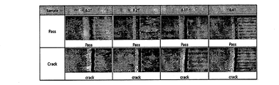
단차로 사용할 0.1t(100㎛), 0.2t(200㎛), 0.3t(300㎛), 0.4t(400㎛)의 FR4막대를 폭 5㎜, 길이 25㎝의 크기로 재단하였다. 재단된 FRP 막대를 두께 순서로 Cu1.0Oz 위에 20㎜ 간격으로 배열한 후 양 끝단을 내열 테이프로 고정하였다. 실시예 1 내지 6의 박막 코팅형 절연필름과 비교예 6의 커버레이를 배열한 FRP 막대 위에 접착층을 올려 놓고 열프레스(60min. at 150℃, 30㎏/㎠)로 가온 가압하여 평가용 시료를 제작하여 FR4 에치(Edge)부위를 현미경으로 관찰하여 크랙 유무를 평가하였다(도 7).0.1t (100 µm), 0.2t (200 µm), 0.3t (300 µm) and 0.4t (400 µm) FR4 rods used as steps were cut to a size of 5 mm in width and 25 cm in length. The cut FRP rods were arranged at intervals of 20 mm over Cu 1.0 Oz in thickness order and both ends were fixed with heat resistant tape. The sample for evaluation was heated and pressurized with a heat press (60min. At 150 ° C, 30kg / cm 2) by placing an adhesive layer on the FRP rod in which the thin film-coated insulating films of Examples 1 to 6 and the coverlay of Comparative Example 6 were arranged. After fabrication, the FR4 edge was observed under a microscope to evaluate the presence of cracks (FIG. 7).
실험예 5: 표면 저항Experimental Example 5: Surface Resistance
상기 표 1 및 2에 표기한 각각의 평가시료의 절연층 면에 표면저항측정기(SRM-110, Wolfgang Warmbier)를 올려 5곳을 측정하여 표시된 저항값의 평균을 표기하였다.The surface resistance measuring instrument (SRM-110, Wolfgang Warmbier) was placed on the insulating layer surface of each of the evaluation samples shown in Tables 1 and 2, and 5 points were measured to indicate the average of the displayed resistance values.
실험예 6: 단자 충진성Experimental Example 6: Terminal Fillability
상기 표 1 및 2에 표기한 각각의 평가시료를 단면 커팅하여 인쇄회로기판과 커버레이의 충진성을 체크하였다. 충진성 평가는 단면을 절단하여 인접한 회로간의 공간을 절연층과 접착층이 충진된 정도를 평가하였다. 평가척도는 인접한 배선의 공간에 충진된 면적을 %로 표기하였다(도 8).The evaluation samples shown in Tables 1 and 2 were cross-sectional cut to check the filling properties of the printed circuit board and the coverlay. Fillability evaluation evaluated the degree of filling the insulating layer and the adhesive layer in the space between adjacent circuits by cutting the cross section. Evaluation scale was expressed in% the area filled in the space of the adjacent wiring (Fig. 8).
실험예 7: 굴곡성 평가Experimental Example 7: Evaluation of Flexibility
상기 표 1 및 2에 표기한 각각의 평가시료를 Solder(60sec. at 260℃) 후 인쇄회로 배선면(copper pattern side) 배선의 수직방향 부위를 180도 손가락으로 강하게 접은 다음 접힌 부위를 역방향으로 180도 접는 것을 1회로 하였다. 동일 방법으로 10회를 진행하여 1회, 5회, 10회 때마다 크랙 유무를 관찰하였다(도 9). Solder (60 sec. At 260 ° C) of each of the evaluation samples shown in Tables 1 and 2, and then fold the vertical part of the copper pattern side wiring strongly with a 180 degree finger, and then reverse the folded part by 180 degrees. The folding was done once. 10 times in the same manner was observed for the presence of cracks once, 5 times, 10 times (Fig. 9).
실험예 8: 탄성 시험Experimental Example 8: Elasticity Test
상기 표 1 및 2에 표기한 각각의 평가시료를 스프링백 테스터(Model: BMSCF-360, 비엠에스테크)로 평가하여 그 수치를 기록하였다.Each of the evaluation samples shown in Tables 1 and 2 was evaluated with a springback tester (Model: BMSCF-360, BMS Tech) and the numerical values were recorded.
상기 실험예 1 내지 8에 따른 평가 방법에 따라, 상기 제작된 실시예 1 내지 6 및 비교예 1 내지 6을 평가한 결과를 표 3에 나타내었다.According to the evaluation method according to Experimental Examples 1 to 8, the results of evaluating the produced Examples 1 to 6 and Comparative Examples 1 to 6 are shown in Table 3.
| 실시예 1Example 1 | 실시예 2 Example 2 | 실시예 3Example 3 | 실시예 4Example 4 | 실시예 5Example 5 | 실시예 6Example 6 | 비교예 1Comparative Example 1 | 비교예 2Comparative Example 2 | 비교예 3Comparative Example 3 | 비교예 4Comparative Example 4 | 비교예 5Comparative Example 5 | 비교예 6Comparative Example 6 | ||
| 솔더 내열성Solder heat resistance | PassPass | PassPass | PassPass | PassPass | PassPass | PassPass | 변색discoloration | 변색discoloration | PassPass | 변색discoloration | 변색discoloration | 들뜸Uplifting | |
| 환경 신뢰성Environmental reliability | PassPass | PassPass | PassPass | PassPass | PassPass | PassPass | 변색discoloration | 변색discoloration | PassPass | 변색discoloration | PassPass | PassPass | |
| 내약품성Chemical resistance | IPAIPA | PassPass | PassPass | PassPass | PassPass | PassPass | PassPass | PassPass | PassPass | PassPass | PassPass | PassPass | PassPass |
| H2SO4 H 2 SO 4 | PassPass | PassPass | PassPass | PassPass | PassPass | PassPass | 산화Oxidation | 산화Oxidation | PassPass | 산화Oxidation | 산화Oxidation | PassPass | |
| NaOHNaOH | PassPass | PassPass | PassPass | PassPass | PassPass | PassPass | 들뜸Uplifting | 들뜸Uplifting | 들뜸Uplifting | 들뜸Uplifting | 들뜸Uplifting | 들뜸Uplifting | |
| 단차크랙Step crack | 0.1t0.1t | PassPass | PassPass | PassPass | PassPass | PassPass | PassPass | N/AN / A | N/AN / A | N/AN / A | N/AN / A | N/AN / A | PassPass |
| 0.2t0.2t | PassPass | PassPass | PassPass | PassPass | PassPass | PassPass | N/AN / A | N/AN / A | N/AN / A | N/AN / A | N/AN / A | PassPass | |
| 0.3t0.3t | CrackCrack | PassPass | PassPass | PassPass | CrackCrack | PassPass | N/AN / A | N/AN / A | N/AN / A | N/AN / A | N/AN / A | PassPass | |
| 0.4t0.4t | CrackCrack | PassPass | CrackCrack | PassPass | CrackCrack | CrackCrack | N/AN / A | N/AN / A | N/AN / A | N/AN / A | N/AN / A | PassPass | |
| 표면 저항 (Ω)Surface resistance (Ω) | 1012 10 12 | 1012 10 12 | 1012 10 12 | 1012 10 12 | 1012 10 12 | 1012 10 12 | 103 10 3 | 108 10 8 | 1012 10 12 | 107 10 7 | 1012 10 12 | 1012 10 12 | |
| 단차 충진 (%)Step filling (%) | 90%90% | 87%87% | 90%90% | 86%86% | 92%92% | 92%92% | 100%100% | 100%100% | 100%100% | 100%100% | 100%100% | 57%57% | |
| 굴곡 횟수 평가Bend count evaluation | 10회 Pass10 pass | 10회 Pass10 pass | 10회 Pass10 pass | 10회 Pass10 pass | 10회 Pass10 pass | 10회 Pass10 pass | 5회Crack5th Crack | 5회Crack5th Crack | 1회Crack1 crack | 5회Crack5th Crack | 1회Crack1 crack | 10회 Pass10 pass | |
| 탄성 시험 (g.f/㎠)Elasticity test (g.f / ㎠) | 10.110.1 | 12.512.5 | 10.610.6 | 12.812.8 | 10.410.4 | 12.612.6 | 8.58.5 | 11.411.4 | 16.216.2 | 14.514.5 | 18.518.5 | 20.520.5 | |
이상으로 본 발명 내용의 특정한 부분을 상세히 기술하였는바, 당업계의 통상의 지식을 가진 자에게 있어서 이러한 구체적 기술은 단지 바람직한 실시태양일 뿐이며, 이에 의해 본 발명의 범위가 제한되는 것이 아닌 점은 명백할 것이다. 따라서, 본 발명의 실질적인 범위는 첨부된 청구항들과 그것들의 등가물에 의하여 정의된다고 할 것이다.As described above in detail specific parts of the present invention, it is apparent to those of ordinary skill in the art that such specific descriptions are merely preferred embodiments, and thus the scope of the present invention is not limited thereto. something to do. Thus, the substantial scope of the present invention will be defined by the appended claims and their equivalents.
[부호의 설명][Description of the code]
11: 캐리어 필름11: carrier film
22: 절연층22: insulation layer
33: 접착층33: adhesive layer
44: 보호필름44: protective film
1: 인쇄회로 금속패턴1: printed circuit metal pattern
2: 기판2: substrate
본 발명은 인쇄회로의 금속 단차 충진성이 우수하며 응력이 낮은 박막 코팅형 절연필름 및 이의 제조방법을 상세히 설명한다.The present invention will be described in detail a thin film coating insulating film and a method of manufacturing a low-stress filled metal step of the printed circuit.
기존 커버레이 필름은 일반적으로 배선 부분을 보호할 목적으로 사용되는 것으로 폴리이미드 수지 등의 합성수지를 이용한 필름(절연층)과 접착제층을 적층하여 제조한다. 이러한 필름형 커버레이는 인쇄회로기판(PCB)의 배선부에 커버레이의 접착제층을 올려 놓고 열프레스를 이용하여 합지 적층하여 사용한다. 종래에 사용되는 커버레이는 필름 기재를 절연층으로 이용하고 있어 인쇄회로 배선간의 공간 충진율이 낮다. 배선 두께에 의한 단차 충진성이 낮아 그 틈새로 도금액이나 세정액이 침투하여 회로패턴을 부식 시키거나 솔더 시에 들뜨는 문제가 나타나고 있다. 또한 박막의 필름 제조가 어렵고 한정된 재료를 사용할 수 밖에 없어 그 가격이 높다. 또한 PI필름을 이용한 기존의 커버레이는 탄성이 높아 필요 시 절연페이스트를 사용하여 추가 공정이 필요하며 이것으로 인한 공정 불량도 나타나고 있다. Existing coverlay film is generally used for the purpose of protecting the wiring part and is manufactured by laminating a film (insulating layer) and an adhesive layer using synthetic resin such as polyimide resin. Such a film type coverlay is used by laminating an adhesive layer of a coverlay on a wiring portion of a printed circuit board (PCB) and laminating using a hot press. The coverlay used in the related art uses a film base material as an insulating layer, so the space filling rate between printed circuit wirings is low. It is a problem that the plating solution or the cleaning liquid penetrates into the gap and the circuit pattern is corroded or the solder is lifted due to the gap filling due to the thickness of the wiring. In addition, it is difficult to manufacture a film of a thin film and the use of a limited material has a high price. In addition, existing coverlays using PI film have high elasticity and require additional processing using insulating pastes, resulting in process defects.
본 발명에서는 절연용 필름을 사용하지 않고 캐리어 필름을 사용하여 다양한 고분자 재료를 절연층으로 사용함으로써 절연필름보다 생산성이 높고 저렴하며 우수한 물성의 박막 코팅형 절연필름을 제조한다. In the present invention, by using various polymer materials as an insulating layer using a carrier film without using an insulating film, a thin film-coated insulating film having higher productivity, lower cost, and better physical properties than an insulating film is manufactured.
본 발명에서 사용되는 캐리어 필름은 절연수지 용액을 코팅하기 위한 기재로서 이용되어 박막의 절연 수지층의 경화 및 건조에 사용된다. 또한 제조한 박막 코팅형 절연필름을 인쇄회로의 배선 보호를 위해 부착 시에 위치 가이드 역할을 하여 박막의 코팅형 절연필름이 구김없이 정해진 위치에 적층될 수 있도록 가이드(Guide) 역할도 할 수 있다.The carrier film used in the present invention is used as a base material for coating the insulating resin solution and used for curing and drying the insulating resin layer of the thin film. In addition, the thin film-coated insulating film may serve as a guide when the thin film-coated insulating film is attached to protect the wiring of the printed circuit so that the thin film-coated insulating film may be stacked at a predetermined position without wrinkles.
본 발명은 일 관점에서, 캐리어 필름; 상기 캐리어 필름의 일면에 형성된 절연층; 상기 절연층에 형성된 접착층; 및 상기 접착층 상에 형성된 보호필름을 포함하는 박막 코팅형 절연필름에 관한 것이다(도 1). 여기서, 박막 코팅형 절연필름은 캐리어 필름을 커버레이로 사용할 수 있다.The present invention in one aspect, a carrier film; An insulation layer formed on one surface of the carrier film; An adhesive layer formed on the insulating layer; And it relates to a thin film coating type insulating film comprising a protective film formed on the adhesive layer (Fig. 1). Here, the thin film coating insulation film may use a carrier film as a coverlay.
본 발명은 또한, (a) 캐리어 필름에 절연층을 형성하는 단계; (b) 상기 절연층에 접착층을 형성하는 단계; 및 (c) 상기 접착층에 보호필름을 합지하는 단계를 포함하는 충진성이 우수하고 탄성률이 낮은 박막 코팅형 절연필름의 제조방법에 관한 것이다. 여기서, 박막 코팅형 절연필름은 캐리어 필름을 커버레이로 사용할 수 있다.The present invention also comprises the steps of (a) forming an insulating layer on the carrier film; (b) forming an adhesive layer on the insulating layer; And (c) laminating a protective film on the adhesive layer, and a method of manufacturing a thin film-coated insulating film having excellent filling properties and low elastic modulus. Here, the thin film coating insulation film may use a carrier film as a coverlay.
본 발명의 박막 코팅형 절연필름은 표면에 절연층을 직접 코팅한 캐리어 필름을 사용하여 절연필름을 제조함으로써, 즉 PI 필름 등의 필름류를 사용하지 않고 절연필름을 제조함으로써, 충진률이 75% 이상으로 충진성이 우수하고, 응력이 낮아 탄성계수가 15g.f/㎠ 이하라는 것에 핵심적인 기술적 특징이 있다.In the thin film coating type insulating film of the present invention, the insulating film is manufactured by using a carrier film coated with an insulating layer directly on its surface, that is, the insulating film is manufactured without using films such as PI films, and thus the filling rate is 75% or more. The key technical characteristics are that the filling property is excellent, and the stress is low, the elastic modulus is 15 g.f / cm 2 or less.
형성된 금속회로부 공간(space)이 절연체로 채워지지 않으면 도금공정에서 도금액 및 수세액이 회로부 말단부(edge) 스페이스로 스며들어 SMT(Surface Mount Technolongy)공정에서 기화 팽창하여 커버레이가 들뜨는 문제가 나타나고 커버레이의 들뜸이 없어도 침투된 액제로 인해 금속회로가 산화되어 제품의 내구성에 문제가 발생한다.If the formed metal circuit part space is not filled with an insulator, the plating solution and flushing liquid penetrate into the edge part of the circuit part in the plating process and vaporize and expand in the Surface Mount Technolongy (SMT) process. Even without lifting, the penetrated liquid causes oxidation of the metal circuit, causing problems in the durability of the product.
PCB제조 공정에서 나타나는 상기의 문제는 금속회로의 형상 및 회로 두께, 회로 선폭, 회로 간격(space) 등의 다양한 인자로 인해 나타난다. 따라서 상기의 문제를 근원적인 해결이 필요한 사항이다. PI필름을 사용한 커버레이의 금속회로 스페이스의 충진율은 60% 미만으로 본 발명을 통하여 스페이스 충진율이 75% 이상인 경우에는 상기와 같은 들뜸이나 도금공정에서의 액침투가 나타나지 않는 것을 확인하였다.The above problems in the PCB manufacturing process are caused by various factors such as the shape and circuit thickness of the metal circuit, the circuit line width, and the circuit space. Therefore, the above-mentioned problem is a fundamental solution. The fill rate of the metal circuit space of the coverlay using the PI film is less than 60%, and through the present invention, when the space filling rate is 75% or more, it was confirmed that the above-mentioned lifting or immersion in the plating process did not appear.
한편 디스플레이패널(display panel) 또는 터치패널(Touch panel)을 ACF(Anisotropic Conductive Film)로 FPCB와 연결하는 작업을 수행한다. 특히 최근 디스플레이의 고해상도와 박막, 경량화의 요구로 미세화된 회로로 인해 ACF의 부착면적이 줄어들어 상대적으로 낮은 부착력을 갖게 되었고, 공정 조건 또한 기존 보다 저온 저압의 조건으로 제조하여 부착력이 더 낮아졌다. 이러한 부착력 저하는 탄성이 높은 FPCB를 사용하는 경우 외부 충격에 의해 단락이 보다 쉽게 발생할 수 있어서 탄성율이 낮은 절연페이스트를 굴곡부위에 스크린 프린터로 프린팅하여 탄성을 낮춰 ACF의 부착 신뢰성을 보완하고 있다. 현재 사용되는 절연페이스트는 통상 건조두께 25 내지 30㎛으로 사용되고 있으며 절연페이스트 두께 30㎛일 때 탄성계수가 16g.f/㎠ 내지 18g.f/㎠이다. 이에 본 발명에서는 절연필름이 탄성계수 15g.f/㎠를 갖는 것을 특징으로 한다. 탄성계수가 낮은 절연필름은 기존 PI필름의 커버레이를 적층한 후 절연페이스트를 도포하는 공정을 대체하여 단일 공정으로 탄성계수가 낮은 연성인쇄회로를 제조할 수 있어서 공정비용 절감 및 제조 수율 향상으로 제조비용을 절감할 수 있고, 제품의 내구성을 향상시킬 수 있다. Meanwhile, a display panel or a touch panel is connected to the FPCB with an anisotropic conductive film (ACF). In particular, due to the miniaturization of the display due to the high resolution, thin film, and light weight of displays, the adhesion area of ACF is reduced, resulting in relatively low adhesion, and the process conditions are also manufactured at low temperature and low pressure. In the case of using a high elastic FPCB, such deterioration in adhesion strength can be easily caused by an external impact. Thus, an insulating paste having a low modulus of elasticity is printed on a bent portion by a screen printer to lower the elasticity to compensate for the attachment reliability of the ACF. Insulation pastes currently used are typically used with a dry thickness of 25 to 30 μm and have an elastic modulus of 16 g · f / cm 2 to 18 g.f / cm 2 when the thickness of the insulation paste is 30 μm. In the present invention, the insulating film is characterized in that it has an elastic modulus of 15g.f / ㎠. Insulation film with low elastic modulus can be manufactured by reducing the process cost and improving production yield because it can manufacture flexible printed circuit with low elastic modulus in a single process by replacing the coverlay of the PI film and then applying the insulation paste. The cost can be reduced and the durability of the product can be improved.
본 발명에 있어서, 상기 절연층은 상기 캐리어 필름을 사용한 코팅방법으로 형성되는 것을 특징으로 할 수 있다.In the present invention, the insulating layer may be formed by a coating method using the carrier film.
본 발명에 있어서, 상기 접착층은 상기 절연층에 접착 수지를 직접 적층하거나, 이형성을 갖는 다른 필름에 접착층을 형성하고 이를 상기 절연층과 합지하여 제조되는 것을 특징으로 할 수 있다(도 2 및 3).In the present invention, the adhesive layer may be prepared by directly laminating an adhesive resin on the insulating layer or by forming an adhesive layer on another film having releasability and laminating it with the insulating layer (FIGS. 2 and 3). .
본 발명에 있어서, 상기 캐리어 필름은 PET 필름, 반광(semi-matt) PET 필름, 무광(matt) PET 필름, PEN 필름, PES 필름, TPU 필름, 나일론(Nylon) 필름, PVC 필름, 합성 종이 및 합성 수지가 코팅된 종이(resin coated paper)로 구성된 군에서 선택된 하나 이상인 것을 특징으로 할 수 있으나, 이에 한정되는 것은 아니다. 바람직하게는 가격이 낮고 종류가 다양한 PET 필름이 사용될 수 있다. 또한 캐리어 필름의 표면이 이형코팅된 것과 처리되지 않은 것 모두가 사용될 수 있다. 캐리어 필름의 표면처리 유무는 가접 또는 열 프레스 이후 캐리어 필름의 제거성에 따라 선택된다. 또한 캐리어 필름의 열 프레스 조건(60분, 150℃, 30 kg/cm2)에서 열변형률이 1% 미만이어야 한다. 열변형률이 이보다 높으면 타발된 박막 코팅형 절연필름의 치수 불량으로 정확한 위치에 부착할 수 없고 열프레스 후 캐리어 필름의 제거 시에 절연 수지와 붙어서 박리력이 높아지거나 박리가 안 되는 문제가 있다.In the present invention, the carrier film is a PET film, semi-matt PET film, matt PET film, PEN film, PES film, TPU film, Nylon film, PVC film, synthetic paper and synthetic The resin may be characterized in that at least one selected from the group consisting of coated paper (resin coated paper), but is not limited thereto. Preferably, low cost and various types of PET film may be used. It is also possible to use both release coated and untreated surfaces of the carrier film. The presence or absence of surface treatment of the carrier film is selected according to the removal property of the carrier film after temporary welding or hot pressing. In addition, the heat deformation rate of the carrier film (60 minutes, 150 ℃, 30 kg / cm 2 ) should be less than 1%. If the thermal strain is higher than this, there is a problem in that it cannot be attached to the correct position due to the poor dimension of the punched thin film-coated insulating film, and the peeling force is increased or cannot be peeled off due to the insulation resin when the carrier film is removed after hot pressing.
본 발명에 있어서, 상기 캐리어 필름의 두께가 바람직하게는 20 내지 125 μm인 것을 특징으로 할 수 있다. 두께 20㎛ 미만은 박막 코팅형 절연필름을 인쇄회로에 적층할 때 휨이나 접힘으로 타발 위치에 맞춰서 적층하기 어렵고 박막에 의한 주름 발생의 문제가 있다. 또한 두께가 125㎛를 초과할 경우에는 열프레스 후 금속회로의 단차 충진성에 문제가 있고 박막 코팅형 절연필름의 타발 공정에서 절단부위의 찢김(Edge Burr) 불량 문제가 있다. In the present invention, the thickness of the carrier film is preferably 20 to 125 μm. When the thickness is less than 20㎛ the thin film coating insulation film is laminated on the printed circuit it is difficult to be laminated in accordance with the punching position by bending or folding, there is a problem of wrinkles caused by the thin film. In addition, when the thickness exceeds 125㎛ there is a problem in the step filling of the metal circuit after the hot press, and there is a problem of poor edge burrs in the punching process of the thin film coating insulation film.
본 발명에 있어서, 상기 캐리어 필름은 가접 후 또는 핫 프레스 후에 제거하여 인쇄회로기판(PCB)의 커버레이(Coverlay)로 적용된다(도 4).In the present invention, the carrier film is removed after the temporary welding or hot pressing to be applied as a coverlay of a printed circuit board (PCB) (FIG. 4).
본 발명은 캐리어 필름을 사용함으로써 고가의 폴리이미드(Polyimide) 필름을 사용하지 않고 다양한 고분자 절연 재료를 사용할 수 있어 생산성 및 가격적인 장점이 있다.The present invention can be used in a variety of polymer insulating materials without using an expensive polyimide (Polyimide) film by using a carrier film there is an advantage in productivity and cost.
본 발명에 있어서, 상기 절연층의 두께가 바람직하게는 2 내지 12 μm인 것을 특징으로 할 수 있다. 두께가 2㎛ 미만은 인쇄회로 금속 배선 단차 부위에서 열프레스 후 찢김이 나타나고 두께 12㎛ 초과의 경우에는 금속배선부의 단차 충진성이 낮아지는 문제가 발생하고 두께 증가에 따른 경화 시간이 길어 생산성이 낮아지며 절연수지 용액 도포량이 많아 가격이 높아진다.In the present invention, the thickness of the insulating layer is preferably 2 to 12 μm. If the thickness is less than 2㎛, tearing occurs after the hot press at the printed circuit metal wiring step, and if the thickness is more than 12㎛, there is a problem that the step filling performance of the metal wiring portion is lowered. The amount of insulation resin solution applied increases the price.
본 발명에 있어서, 상기 절연층은 열경화성 수지(thermoset resin), 열가소성 수지(thermoplastic resin) 및 광경화형 수지(photocurable resin)로 구성된 군에서 선택된 하나 이상으로 이루어진 것을 특징으로 할 수 있다. 구체적으로, 상기 절연층은 에폭시 수지(epoxy resin), 폴리우레탄 수지(polyurethane resin), 폴리에스터 수지(polyester resin), 폴리이미드 수지(polyimide resin), 아마이드 수지(amide resin), 페녹시 수지(phenoxy resin), 노블락 수지(novlac resin), 멜라민 수지(melamine resin), 셀룰로이드 아세트산 수지(celluloid acetate resin), 알키드 수지(alkyd resin), 로진 에스터 수지(rosin ester resin), 말레익 수지(maleic resin), 에틸렌 아크릴레이트 수지(ethylene acrylate resin), 우레탄 아크릴레이트 수지(urethane acrylate resin), 에폭시 아크릴레이트 수지(epoxy acrylate resin) 및 이들의 변성 수지로 구성된 군에서 선택된 하나 이상으로 이루어진 것을 특징으로 할 수 있으나, 이에 한정되는 것은 아니다.In the present invention, the insulating layer may be made of one or more selected from the group consisting of a thermoset resin, a thermoplastic resin, and a photocurable resin. Specifically, the insulating layer may be an epoxy resin, a polyurethane resin, a polyester resin, a polyimide resin, an amide resin, or a phenoxy resin. resins, novlac resins, melamine resins, celluloid acetate resins, alkyd resins, rosin ester resins, maleic resins, It may be characterized by consisting of at least one selected from the group consisting of ethylene acrylate resin (ethylene acrylate resin), urethane acrylate resin (urethane acrylate resin), epoxy acrylate resin (epoxy acrylate resin) and modified resin thereof, It is not limited to this.
본 발명에 있어서, 상기 절연층 수지에 난연제와 계면활성제, 부착증진제 등을 사용할 수 있다. 난연제로는 TEP(Triethyl phosphate), RDP(Resorcinol bis(diphenyl phosphate), TCP(Tricresyl phosphate), IPPP(Isopropylphenyl phosphate) 등의 인계난연제, 또는 MCA(Melamine cyanurate), ATO(Aluminium trioxide), ATH(Aluminium trihydrate) 등의 무기난연제를 사용할 수 있다. 본 발명에서는 난연제를 수지대비 15% 사용하여 난연성을 확보하였다. 또한 캐리어 필름에 코팅 시 코팅 도막의 핀홀(Pin hole) 방지 및 레벨링 특성을 위해 실리콘계 계면활성제를 사용할 수 있다. 인쇄회로 층간 부착력 향상을 위해 실란계 커플링제 또는 트리아진 유도체(Triazine derivative)를 사용할 수 있다. In the present invention, a flame retardant, a surfactant, an adhesion promoter and the like can be used for the insulating layer resin. Flame retardants include phosphorus flame retardants such as Triethyl phosphate (TEP), Resorcinol bis (diphenyl phosphate), RDP (Tricresyl phosphate), IPPP (Isopropylphenyl phosphate), or MCA (Melamine cyanurate), ATO (Aluminium trioxide) and ATH (Aluminium) inorganic flame retardants such as trihydrate, etc. In the present invention, the flame retardant is 15% compared to the resin to secure flame retardancy, and a silicone-based surfactant for preventing pin holes and leveling characteristics of the coating film when coating the carrier film. In order to improve adhesion between printed circuits, a silane coupling agent or a triazine derivative may be used.
본 발명에 있어서, 상기 접착층이 반경화(B-stage) 상태인 것을 특징으로 할 수 있다. 상기 접착층은 코팅 건조 후 반경화를 유지하여야 하며 인쇄회로와 적층한 후 열프레스로 완전경화(C-stage)되어야 한다. In the present invention, the adhesive layer may be characterized in that the semi-cured (B-stage) state. The adhesive layer should remain semi-cured after the coating is dried and should be completely cured by heat press after lamination with a printed circuit.
본 발명에 있어서, 상기 접착층은 상기 절연층 수지와 동일하거나 상이한 수지로 이루어질 수 있다.In the present invention, the adhesive layer may be made of the same or different resin as the insulating layer resin.
본 발명에 있어서, 상기 접착층은 접착층의 기능 향상을 위하여 부착증진제와 계면활성제를 포함할 수 있다.In the present invention, the adhesive layer may include an adhesion promoter and a surfactant to improve the function of the adhesive layer.
본 발명에 있어서, 상기 접착층의 코팅 건조 후 두께가 바람직하게는 3 내지 30 μm인 것을 특징으로 할 수 있다. 건조 후 두께가 3㎛ 미만일 경우 열프레스 공정에서 수지 흐름(resin flow)성이 낮아 회로배선의 단차 충진성이 낮고 인쇄회로부와의 부착력이 낮아지는 문제가 있다. 한편 접착층이 건조 두께가 30㎛를 초과하는 경우에는 열프레스 공정에서 과도한 수지 흐름으로 도금단자부의 오염 및 미도금이 발생하는 문제가 있다.In the present invention, the thickness after coating drying of the adhesive layer may be characterized in that preferably 3 to 30 μm. When the thickness is less than 3㎛ after drying, there is a problem that the resin flow (resin flow) in the heat press process is low, the step filling of the circuit wiring is low, and the adhesion to the printed circuit portion is lowered. On the other hand, when the adhesive layer has a dry thickness of more than 30 μm, there is a problem that contamination and unplating of the plating terminal part occur due to excessive resin flow in the heat press process.
본 발명에 있어서, 상기 절연층 및 접착층은 캐리어 필름을 이용하여 단일코팅으로 형성되는 것을 특징으로 할 수 있다.In the present invention, the insulating layer and the adhesive layer may be formed by a single coating using a carrier film.
본 발명에 따르면, 종래에 PI필름이나 절연 페이스트를 사용하던 종래와는 달리, PI필름이나 절연 페이스트를 사용하지 않고, 캐리어 필름(carrier film) 및 이를 이용하여 절연 수지를 코팅하여 절연층(insulation layer)을 형성하고, 그 일면에 반경화(B-stage) 상태의 접착층(adhesive layer)을 포함하는 박막 코팅형 절연필름(insulation film)과 절연기능과 접착기능을 갖는 수지 용액을 캐리어 필름 일면에 코팅하여, 인쇄회로의 단차 충진성이 우수하고 탄성률이 낮은 박막 코팅형 절연필름 및 그 제조방법이 제공된다.According to the present invention, unlike a conventional film using an PI film or an insulating paste, without using a PI film or an insulating paste, a carrier film and an insulating resin is coated using the insulating layer (insulation layer) ) Is coated on one side of the carrier film with a thin film coated insulation film including an adhesive layer in a B-stage state and a resin solution having an insulating function and an adhesive function on one surface thereof. As a result, a thin film-coated insulating film having excellent step filling ability of a printed circuit and a low elastic modulus and a method of manufacturing the same are provided.
또한 본 발명에 따르면, 인쇄회로 배선부의 충진율이 75% 이상이고 탄성계수가 15g.f/㎠ 이하인, 인쇄회로의 단차 충진성이 우수하고 탄성률이 낮은 박막 코팅형 절연필름 및 그 제조방법이 제공된다.According to the present invention, there is provided a thin film-coated insulating film having excellent step filling performance and low elastic modulus of a printed circuit having a filling rate of 75% or more and an elastic modulus of 15 g · f / cm 2 or less, and a method of manufacturing the same. .
구체적으로 본 발명에 따르면 박막 코팅형 절연필름은 금속회로의 단차에 충진성이 우수하여 미세회로의 도금 공정에서 회로내부로 도금액의 침투 및 도금 세정액이 침투하지 않아 단자부 들뜸이 나타나지 않고 솔더(Solder)공정에서 열에 의한 층간박리(Delamination)를 방지할 수 있다. 또한 종래 PI필름 등의 필름류와 달리 본 발명에 따른 박막 코팅형 절연필름은 응력이 낮은 특성으로 낮은 탄성을 필요로 하는 인쇄회로기판에 적용할 수 있다. 아울러 본 발명에 따르면 탄성이 낮은 박막 코팅형 절연필름을 적층함으로써 절연 페이스트를 사용하지 않고 커버레이 적층 단일공정으로 접힘 부위를 제조함으로써 공정을 단축할 수 있고 절연 페이스트를 사용하지 않아 절연 페이스트 프린팅 공정에서의 액튐 불량, 열경화 시의 액흐름, 경화 후 크랙의 문제에 따른 불량을 방지할 수 있게 된다. Specifically, according to the present invention, the thin film coating insulating film has excellent filling property in the step of the metal circuit, and thus, the plating liquid and the plating cleaning liquid do not penetrate into the circuit in the plating process of the micro circuit, so that the terminal part does not appear and the solder (Solder) does not appear. Delamination due to heat in the process can be prevented. In addition, unlike conventional films such as PI film, the thin film-coated insulating film according to the present invention can be applied to a printed circuit board requiring low elasticity due to low stress characteristics. In addition, according to the present invention, by laminating a thin elastic coating film having a low elasticity, the process can be shortened by manufacturing a folded portion in a single step of covering the coverlay without using an insulation paste, and in an insulation paste printing process without using an insulation paste. It is possible to prevent the poor liquid due to the liquid problem, the liquid flow during heat curing, and the problem of cracks after curing.
Claims (28)
- 캐리어 필름;Carrier film;상기 캐리어 필름의 일면에 형성된 절연층;An insulation layer formed on one surface of the carrier film;상기 절연층에 형성된 접착층; 및An adhesive layer formed on the insulating layer; And상기 접착층 상에 형성된 보호필름을 포함하는 박막 코팅형 절연필름.Thin film coating insulating film comprising a protective film formed on the adhesive layer.
- 제1항에 있어서, 충진률이 75% 이상인 것을 특징으로 하는 박막 코팅형 절연필름.The thin film coating insulation film according to claim 1, wherein the filling rate is 75% or more.
- 제1항에 있어서, 탄성계수가 15g.f/㎠ 이하인 것을 특징으로 하는 박막 코팅형 절연필름.The thin film-coated insulating film according to claim 1, wherein the modulus of elasticity is 15 g · f / cm 2 or less.
- 제1항에 있어서, 상기 절연층은 상기 캐리어 필름을 사용한 코팅방법으로 형성되는 것을 특징으로 하는 박막 코팅형 절연필름.The method of claim 1, wherein the insulating layer is a thin film coating type insulating film, characterized in that formed by the coating method using the carrier film.
- 제1항에 있어서, 상기 캐리어 필름은 PET 필름, 반광 PET 필름, 무광 PET 필름, PEN 필름, PES 필름, TPU 필름, 나일론 필름, PVC 필름, 합성 종이 및 합성 수지가 코팅된 종이로 구성된 군에서 선택된 하나 이상인 것을 특징으로 하는 박막 코팅형 절연필름.The method of claim 1, wherein the carrier film is selected from the group consisting of PET film, semi-gloss PET film, matte PET film, PEN film, PES film, TPU film, nylon film, PVC film, synthetic paper and synthetic resin coated paper Thin film coating insulation film, characterized in that one or more.
- 제1항에 있어서, 상기 캐리어 필름의 두께가 20 내지 125 μm인 것을 특징으로 하는 박막 코팅형 절연필름.According to claim 1, wherein the thickness of the carrier film is a thin film coating type insulating film, characterized in that 20 to 125 μm.
- 제1항에 있어서, 상기 절연층의 두께가 2 내지 12 μm인 것을 특징으로 하는 박막 코팅형 절연필름.According to claim 1, wherein the thickness of the insulating layer is a thin film coating type insulating film, characterized in that 2 to 12 μm.
- 제1항에 있어서, 상기 절연층은 열경화성 수지, 열가소성 수지 및 광경화형 수지로 구성된 군에서 선택된 하나 이상으로 이루어진 것을 특징으로 하는 박막 코팅형 절연필름.The thin film coating insulating film of claim 1, wherein the insulating layer is formed of at least one selected from the group consisting of a thermosetting resin, a thermoplastic resin, and a photocurable resin.
- 제1항에 있어서, 상기 절연층은 에폭시 수지, 폴리우레탄 수지, 폴리에스터 수지, 폴리이미드 수지, 아마이드 수지, 페녹시 수지, 노블락 수지, 멜라민 수지, 셀룰로이드 아세트산 수지, 알키드 수지, 로진 에스터 수지, 말레익 수지, 에틸렌 아크릴레이트 수지, 우레탄 아크릴레이트 수지, 에폭시 아크릴레이트 수지 및 이들의 변성 수지로 구성된 군에서 선택된 하나 이상으로 이루어진 것을 특징으로 하는 박막 코팅형 절연필름.The method of claim 1, wherein the insulating layer is epoxy resin, polyurethane resin, polyester resin, polyimide resin, amide resin, phenoxy resin, noblock resin, melamine resin, celluloid acetate resin, alkyd resin, rosin ester resin, male A thin film coating insulation film comprising at least one selected from the group consisting of a blade resin, ethylene acrylate resin, urethane acrylate resin, epoxy acrylate resin and modified resin thereof.
- 제1항에 있어서, 상기 절연층은 에폭시 수지, 폴리우레탄 수지, 폴리에스터 수지, 폴리이미드 수지, 아마이드 수지, 페녹시 수지, 노블락 수지, 멜라민 수지, 셀룰로이드 아세트산 수지, 알키드 수지, 로진 에스터 수지, 말레익 수지, 에틸렌 아크릴레이트 수지, 우레탄 아크릴레이트 수지, 에폭시 아크릴레이트 수지 및 이들의 변성 수지로 구성된 군에서 선택된 하나 이상의 수지; 수산화 알루미늄; 분산제; 및 사이클로헥사논 또는 디메틸 아세트아마이드:로 구성된 절연 조성물을 코팅 방법으로 도포하여 형성되는 것을 특징으로 하는 박막 코팅형 절연필름.The method of claim 1, wherein the insulating layer is epoxy resin, polyurethane resin, polyester resin, polyimide resin, amide resin, phenoxy resin, noblock resin, melamine resin, celluloid acetate resin, alkyd resin, rosin ester resin, male At least one resin selected from the group consisting of a blade resin, ethylene acrylate resin, urethane acrylate resin, epoxy acrylate resin and modified resin thereof; Aluminum hydroxide; Dispersants; And cyclohexanone or dimethyl acetamide: a thin film-coated insulation film, characterized in that formed by applying a coating method.
- 제1항에 있어서, 상기 접착층이 반경화 상태인 것을 특징으로 하는 박막 코팅형 절연필름.The thin film coating insulation film of claim 1, wherein the adhesive layer is in a semi-cured state.
- 제1항에 있어서, 상기 접착층의 두께가 3 내지 30 μm인 것을 특징으로 하는 박막 코팅형 절연필름.According to claim 1, wherein the thickness of the adhesive layer is a thin film coating type insulating film, characterized in that 3 to 30 μm.
- 제1항에 있어서, 상기 접착층은 상기 절연층에 접착 수지를 직접 적층하거나, 이형성을 갖는 다른 필름에 접착층을 형성하고 이를 상기 절연층과 합지하여 제조되는 것을 특징으로 하는 박막 코팅형 절연필름.The thin film coating insulating film of claim 1, wherein the adhesive layer is manufactured by directly stacking an adhesive resin on the insulating layer or forming an adhesive layer on another film having releasability and laminating it with the insulating layer.
- 제1항에 있어서, 상기 절연층 및 접착층은 캐리어 필름을 이용하여 단일코팅으로 형성되는 것을 특징으로 하는 박막 코팅형 절연필름.The thin film-coated insulating film of claim 1, wherein the insulating layer and the adhesive layer are formed by a single coating using a carrier film.
- 다음 단계를 포함하는 박막 코팅형 절연필름의 제조방법:Method of manufacturing a thin film coating insulation film comprising the following steps:(a) 캐리어 필름에 절연층을 형성하는 단계;(a) forming an insulating layer on the carrier film;(b) 상기 절연층에 접착층을 형성하는 단계; 및(b) forming an adhesive layer on the insulating layer; And(c) 상기 접착층에 보호필름을 합지하는 단계.(c) laminating a protective film on the adhesive layer.
- 제15항에 있어서, 상기 박막 코팅형 절연필름의 충진률이 75% 이상인 것을 특징으로 하는 박막 코팅형 절연필름의 제조방법.The method of claim 15, wherein the filling rate of the thin film coating insulating film is 75% or more.
- 제15항에 있어서, 상기 박막 코팅형 절연필름의 탄성계수가 15g.f/㎠ 이하인 것을 특징으로 하는 박막 코팅형 절연필름의 제조방법.The method of claim 15, wherein the elastic modulus of the thin film-coated insulating film is 15 g · f / cm 2 or less.
- 제15항에 있어서, 상기 절연층은 캐리어 필름에 절연 조성물을 코팅하여 형성되는 것을 특징으로 하는 박막 코팅형 절연필름의 제조방법.The method of claim 15, wherein the insulation layer is formed by coating an insulation composition on a carrier film.
- 제15항에 있어서, 상기 캐리어 필름은 PET 필름, 반광 PET 필름, 무광 PET 필름, PEN 필름, PES 필름, TPU 필름, 나일론 필름, PVC 필름, 합성 종이 및 합성 수지가 코팅된 종이로 구성된 군에서 선택된 하나 이상인 것을 특징으로 하는 박막 코팅형 절연필름의 제조방법.The method of claim 15, wherein the carrier film is selected from the group consisting of PET film, semi-gloss PET film, matte PET film, PEN film, PES film, TPU film, nylon film, PVC film, synthetic paper and synthetic resin coated paper Method for producing a thin film coating insulation film characterized in that at least one.
- 제15항에 있어서, 상기 캐리어 필름의 두께가 20 내지 125 μm인 것을 특징으로 하는 박막 코팅형 절연필름의 제조방법.The method of claim 15, wherein the carrier film has a thickness of 20 to 125 μm.
- 제15항에 있어서, 상기 절연층의 두께가 2 내지 12 μm인 것을 특징으로 하는 박막 코팅형 절연필름의 제조방법.The method of claim 15, wherein the thickness of the insulating layer is 2 to 12 μm.
- 제15항에 있어서, 상기 절연층은 열경화성 수지, 열가소성 수지 및 광경화형 수지로 구성된 군에서 선택된 하나 이상으로 이루어진 것을 특징으로 하는 박막 코팅형 절연필름의 제조방법.The method of claim 15, wherein the insulating layer is formed of at least one selected from the group consisting of a thermosetting resin, a thermoplastic resin, and a photocurable resin.
- 제15항에 있어서, 상기 절연층은 에폭시 수지, 폴리우레탄 수지, 폴리에스터 수지, 폴리이미드 수지, 아마이드 수지, 페녹시 수지, 노블락 수지, 멜라민 수지, 셀룰로이드 아세트산 수지, 알키드 수지, 로진 에스터 수지, 말레익 수지, 에틸렌 아크릴레이트 수지, 우레탄 아크릴레이트 수지, 에폭시 아크릴레이트 수지 및 이들의 변성 수지로 구성된 군에서 선택된 하나 이상으로 이루어진 것을 특징으로 하는 박막 코팅형 절연필름의 제조방법.The method of claim 15, wherein the insulating layer is epoxy resin, polyurethane resin, polyester resin, polyimide resin, amide resin, phenoxy resin, noblock resin, melamine resin, celluloid acetate resin, alkyd resin, rosin ester resin, male A method of manufacturing a thin film-coated insulating film, characterized in that consisting of at least one selected from the group consisting of a blade resin, ethylene acrylate resin, urethane acrylate resin, epoxy acrylate resin and modified resin thereof.
- 제15항에 있어서, 상기 절연층은 에폭시 수지, 폴리우레탄 수지, 폴리에스터 수지, 폴리이미드 수지, 아마이드 수지, 페녹시 수지, 노블락 수지, 멜라민 수지, 셀룰로이드 아세트산 수지, 알키드 수지, 로진 에스터 수지, 말레익 수지, 에틸렌 아크릴레이트 수지, 우레탄 아크릴레이트 수지, 에폭시 아크릴레이트 수지 및 이들의 변성 수지로 구성된 군에서 선택된 하나 이상의 수지; 수산화 알루미늄; 분산제; 및 사이클로헥사논 또는 디메틸 아세트아마이드:로 구성된 절연 조성물을 코팅 방법으로 도포하여 형성되는 것을 특징으로 하는 박막 코팅형 절연필름의 제조방법.The method of claim 15, wherein the insulating layer is epoxy resin, polyurethane resin, polyester resin, polyimide resin, amide resin, phenoxy resin, noblock resin, melamine resin, celluloid acetate resin, alkyd resin, rosin ester resin, male At least one resin selected from the group consisting of a blade resin, ethylene acrylate resin, urethane acrylate resin, epoxy acrylate resin and modified resin thereof; Aluminum hydroxide; Dispersants; And cyclohexanone or dimethyl acetamide: which is formed by applying a coating method by a coating method.
- 제15항에 있어서, 상기 접착층이 반경화 상태인 것을 특징으로 하는 박막 코팅형 절연필름의 제조방법.The method of claim 15, wherein the adhesive layer is in a semi-cured state.
- 제15항에 있어서, 상기 접착층의 두께가 3 내지 30 μm인 것을 특징으로 하는 박막 코팅형 절연필름의 제조방법.The method of claim 15, wherein the adhesive layer has a thickness of 3 to 30 μm.
- 제15항에 있어서, 상기 접착층은 상기 절연층에 접착 수지를 직접 적층하거나, 이형성을 갖는 다른 필름에 접착층을 형성하고 이를 상기 절연층과 합지하여 제조되는 것을 특징으로 하는, 박막 코팅형 절연필름의 제조방법.The method of claim 15, wherein the adhesive layer is manufactured by laminating an adhesive resin directly on the insulating layer or forming an adhesive layer on another film having releasability and laminating it with the insulating layer. Manufacturing method.
- 제15항에 있어서, 상기 절연층 및 접착층은 캐리어 필름을 이용하여 단일코팅으로 형성되는 것을 특징으로 하는 박막 코팅형 절연필름의 제조방법.The method of claim 15, wherein the insulating layer and the adhesive layer are formed by a single coating using a carrier film.
Priority Applications (1)
| Application Number | Priority Date | Filing Date | Title |
|---|---|---|---|
| PCT/KR2018/006299 WO2019231028A1 (en) | 2018-06-01 | 2018-06-01 | Insulation film and method for manufacturing insulation film |
Applications Claiming Priority (1)
| Application Number | Priority Date | Filing Date | Title |
|---|---|---|---|
| PCT/KR2018/006299 WO2019231028A1 (en) | 2018-06-01 | 2018-06-01 | Insulation film and method for manufacturing insulation film |
Publications (1)
| Publication Number | Publication Date |
|---|---|
| WO2019231028A1 true WO2019231028A1 (en) | 2019-12-05 |
Family
ID=68698316
Family Applications (1)
| Application Number | Title | Priority Date | Filing Date |
|---|---|---|---|
| PCT/KR2018/006299 WO2019231028A1 (en) | 2018-06-01 | 2018-06-01 | Insulation film and method for manufacturing insulation film |
Country Status (1)
| Country | Link |
|---|---|
| WO (1) | WO2019231028A1 (en) |
Cited By (2)
| Publication number | Priority date | Publication date | Assignee | Title |
|---|---|---|---|---|
| CN113322714A (en) * | 2020-02-28 | 2021-08-31 | 中国科学院成都有机化学有限公司 | Polyimide compound high-temperature aging resistant auxiliary agent, insulating paper and preparation method thereof |
| CN114245582A (en) * | 2021-12-16 | 2022-03-25 | 深圳市昶东鑫线路板有限公司 | Flexible circuit board processing intelligent manufacturing equipment |
Citations (5)
| Publication number | Priority date | Publication date | Assignee | Title |
|---|---|---|---|---|
| JP2001074933A (en) * | 1999-09-01 | 2001-03-23 | Nitto Denko Corp | Surface protective film |
| US20120320542A1 (en) * | 2011-06-16 | 2012-12-20 | Chang-Yong Jeong | Display device and method for manufacturing the same |
| KR20130096025A (en) * | 2012-02-21 | 2013-08-29 | 삼성전기주식회사 | Method of manufacturing flying tail type rigid-flexible printed circuit board and flying tail type rigid-flexible printed circuit board manufactured by the same |
| KR20140074700A (en) * | 2012-12-10 | 2014-06-18 | 남광현 | Functional film and flexible printed circuit board including the same |
| KR20160103502A (en) * | 2015-01-20 | 2016-09-01 | (주)창성 | Electromagnetic wave shielding sheet and manufacturing method of the same |
-
2018
- 2018-06-01 WO PCT/KR2018/006299 patent/WO2019231028A1/en active Application Filing
Patent Citations (5)
| Publication number | Priority date | Publication date | Assignee | Title |
|---|---|---|---|---|
| JP2001074933A (en) * | 1999-09-01 | 2001-03-23 | Nitto Denko Corp | Surface protective film |
| US20120320542A1 (en) * | 2011-06-16 | 2012-12-20 | Chang-Yong Jeong | Display device and method for manufacturing the same |
| KR20130096025A (en) * | 2012-02-21 | 2013-08-29 | 삼성전기주식회사 | Method of manufacturing flying tail type rigid-flexible printed circuit board and flying tail type rigid-flexible printed circuit board manufactured by the same |
| KR20140074700A (en) * | 2012-12-10 | 2014-06-18 | 남광현 | Functional film and flexible printed circuit board including the same |
| KR20160103502A (en) * | 2015-01-20 | 2016-09-01 | (주)창성 | Electromagnetic wave shielding sheet and manufacturing method of the same |
Cited By (3)
| Publication number | Priority date | Publication date | Assignee | Title |
|---|---|---|---|---|
| CN113322714A (en) * | 2020-02-28 | 2021-08-31 | 中国科学院成都有机化学有限公司 | Polyimide compound high-temperature aging resistant auxiliary agent, insulating paper and preparation method thereof |
| CN113322714B (en) * | 2020-02-28 | 2022-12-02 | 中国科学院成都有机化学有限公司 | Polyimide compound high-temperature aging resistant auxiliary agent, insulating paper and preparation method thereof |
| CN114245582A (en) * | 2021-12-16 | 2022-03-25 | 深圳市昶东鑫线路板有限公司 | Flexible circuit board processing intelligent manufacturing equipment |
Similar Documents
| Publication | Publication Date | Title |
|---|---|---|
| WO2011162453A1 (en) | Method for manufacturing electromagnetic shielding film and electromagnetic shielding film manufactured thereby | |
| US20060156542A1 (en) | Method of fabricating rigid flexible printed circuit board | |
| WO2019124624A1 (en) | Electromagnetic wave shielding film, method for manufacturing printed circuit board, and method for manufacturing electromagnetic wave shielding film | |
| WO2019231028A1 (en) | Insulation film and method for manufacturing insulation film | |
| KR101361533B1 (en) | Method for manufacturing electromagnetic wave shield film | |
| WO2018101503A1 (en) | Method for manufacturing printed circuit board and printed circuit board manufactured thereby | |
| WO2016105131A1 (en) | Method for manufacturing electromagnetic wave shielding film for flexible printed circuit board | |
| WO2018151578A1 (en) | Method for manufacturing transfer film including seed layer, method for manufacturing circuit board by selectively etching seed layer, and etching solution composite | |
| WO2012087072A2 (en) | Printed circuit board and method for manufacturing same | |
| WO2018117636A1 (en) | Metal laminate and method for manufacturing same | |
| CN115767876A (en) | Covering film | |
| WO2012053826A1 (en) | Thick layer polyimide metal clad laminate | |
| WO2015105340A1 (en) | Electromagnetic wave shielding film for flexible printed circuit board and manufacturing method therefor | |
| WO2013085229A1 (en) | Printed circuit board and method of manufacturing the same | |
| WO2011010889A2 (en) | Flexible printed circuit board and method for manufacturing the same | |
| JP6883400B2 (en) | Coverlay film | |
| KR102240918B1 (en) | Insulation film and method of manufacturing insulation film | |
| WO2015056880A1 (en) | Method for manufacturing circuit board | |
| WO2018194367A1 (en) | Method for manufacturing printed circuit board | |
| WO2013141611A1 (en) | Semiconductor memory card, printed circuit board for memory card and method of fabricating the same | |
| WO2018186654A1 (en) | Printed circuit board and method for producing same | |
| WO2016117720A1 (en) | Electromagnetic wave shielding sheet and manufacturing method of the same | |
| WO2019124930A1 (en) | Ductile metal laminate plate for touch sensor | |
| KR100752023B1 (en) | Method for manufacturing Rigid-flexible Printed Circuit Board | |
| KR100797675B1 (en) | Adhesive tape of transporting jig for substrate |
Legal Events
| Date | Code | Title | Description |
|---|---|---|---|
| 121 | Ep: the epo has been informed by wipo that ep was designated in this application |
Ref document number: 18920324 Country of ref document: EP Kind code of ref document: A1 |
|
| NENP | Non-entry into the national phase |
Ref country code: DE |
|
| 122 | Ep: pct application non-entry in european phase |
Ref document number: 18920324 Country of ref document: EP Kind code of ref document: A1 |