WO2019230615A1 - センサ及びセンサ付き装置 - Google Patents
センサ及びセンサ付き装置 Download PDFInfo
- Publication number
- WO2019230615A1 WO2019230615A1 PCT/JP2019/020780 JP2019020780W WO2019230615A1 WO 2019230615 A1 WO2019230615 A1 WO 2019230615A1 JP 2019020780 W JP2019020780 W JP 2019020780W WO 2019230615 A1 WO2019230615 A1 WO 2019230615A1
- Authority
- WO
- WIPO (PCT)
- Prior art keywords
- cell
- sensor
- protective layer
- insulating substrate
- wiring board
- Prior art date
- Legal status (The legal status is an assumption and is not a legal conclusion. Google has not performed a legal analysis and makes no representation as to the accuracy of the status listed.)
- Ceased
Links
Images









Classifications
-
- G—PHYSICS
- G06—COMPUTING OR CALCULATING; COUNTING
- G06V—IMAGE OR VIDEO RECOGNITION OR UNDERSTANDING
- G06V40/00—Recognition of biometric, human-related or animal-related patterns in image or video data
- G06V40/10—Human or animal bodies, e.g. vehicle occupants or pedestrians; Body parts, e.g. hands
- G06V40/12—Fingerprints or palmprints
- G06V40/13—Sensors therefor
- G06V40/1329—Protecting the fingerprint sensor against damage caused by the finger
-
- B—PERFORMING OPERATIONS; TRANSPORTING
- B32—LAYERED PRODUCTS
- B32B—LAYERED PRODUCTS, i.e. PRODUCTS BUILT-UP OF STRATA OF FLAT OR NON-FLAT, e.g. CELLULAR OR HONEYCOMB, FORM
- B32B27/00—Layered products comprising a layer of synthetic resin
-
- B—PERFORMING OPERATIONS; TRANSPORTING
- B32—LAYERED PRODUCTS
- B32B—LAYERED PRODUCTS, i.e. PRODUCTS BUILT-UP OF STRATA OF FLAT OR NON-FLAT, e.g. CELLULAR OR HONEYCOMB, FORM
- B32B7/00—Layered products characterised by the relation between layers; Layered products characterised by the relative orientation of features between layers, or by the relative values of a measurable parameter between layers, i.e. products comprising layers having different physical, chemical or physicochemical properties; Layered products characterised by the interconnection of layers
- B32B7/02—Physical, chemical or physicochemical properties
- B32B7/025—Electric or magnetic properties
-
- G—PHYSICS
- G06—COMPUTING OR CALCULATING; COUNTING
- G06F—ELECTRIC DIGITAL DATA PROCESSING
- G06F3/00—Input arrangements for transferring data to be processed into a form capable of being handled by the computer; Output arrangements for transferring data from processing unit to output unit, e.g. interface arrangements
- G06F3/01—Input arrangements or combined input and output arrangements for interaction between user and computer
- G06F3/03—Arrangements for converting the position or the displacement of a member into a coded form
- G06F3/033—Pointing devices displaced or positioned by the user, e.g. mice, trackballs, pens or joysticks; Accessories therefor
- G06F3/0354—Pointing devices displaced or positioned by the user, e.g. mice, trackballs, pens or joysticks; Accessories therefor with detection of two-dimensional [2D] relative movements between the device, or an operating part thereof, and a plane or surface, e.g. 2D mice, trackballs, pens or pucks
-
- G—PHYSICS
- G06—COMPUTING OR CALCULATING; COUNTING
- G06F—ELECTRIC DIGITAL DATA PROCESSING
- G06F3/00—Input arrangements for transferring data to be processed into a form capable of being handled by the computer; Output arrangements for transferring data from processing unit to output unit, e.g. interface arrangements
- G06F3/01—Input arrangements or combined input and output arrangements for interaction between user and computer
- G06F3/03—Arrangements for converting the position or the displacement of a member into a coded form
- G06F3/041—Digitisers, e.g. for touch screens or touch pads, characterised by the transducing means
- G06F3/0416—Control or interface arrangements specially adapted for digitisers
- G06F3/04164—Connections between sensors and controllers, e.g. routing lines between electrodes and connection pads
-
- G—PHYSICS
- G06—COMPUTING OR CALCULATING; COUNTING
- G06F—ELECTRIC DIGITAL DATA PROCESSING
- G06F3/00—Input arrangements for transferring data to be processed into a form capable of being handled by the computer; Output arrangements for transferring data from processing unit to output unit, e.g. interface arrangements
- G06F3/01—Input arrangements or combined input and output arrangements for interaction between user and computer
- G06F3/03—Arrangements for converting the position or the displacement of a member into a coded form
- G06F3/041—Digitisers, e.g. for touch screens or touch pads, characterised by the transducing means
- G06F3/044—Digitisers, e.g. for touch screens or touch pads, characterised by the transducing means by capacitive means
- G06F3/0446—Digitisers, e.g. for touch screens or touch pads, characterised by the transducing means by capacitive means using a grid-like structure of electrodes in at least two directions, e.g. using row and column electrodes
-
- G—PHYSICS
- G06—COMPUTING OR CALCULATING; COUNTING
- G06V—IMAGE OR VIDEO RECOGNITION OR UNDERSTANDING
- G06V40/00—Recognition of biometric, human-related or animal-related patterns in image or video data
- G06V40/10—Human or animal bodies, e.g. vehicle occupants or pedestrians; Body parts, e.g. hands
- G06V40/12—Fingerprints or palmprints
- G06V40/13—Sensors therefor
- G06V40/1306—Sensors therefor non-optical, e.g. ultrasonic or capacitive sensing
-
- H—ELECTRICITY
- H05—ELECTRIC TECHNIQUES NOT OTHERWISE PROVIDED FOR
- H05K—PRINTED CIRCUITS; CASINGS OR CONSTRUCTIONAL DETAILS OF ELECTRIC APPARATUS; MANUFACTURE OF ASSEMBLAGES OF ELECTRICAL COMPONENTS
- H05K1/00—Printed circuits
- H05K1/02—Details
-
- G—PHYSICS
- G06—COMPUTING OR CALCULATING; COUNTING
- G06F—ELECTRIC DIGITAL DATA PROCESSING
- G06F2203/00—Indexing scheme relating to G06F3/00 - G06F3/048
- G06F2203/041—Indexing scheme relating to G06F3/041 - G06F3/045
- G06F2203/04107—Shielding in digitiser, i.e. guard or shielding arrangements, mostly for capacitive touchscreens, e.g. driven shields, driven grounds
Definitions
- Embodiments of the present invention relate to a sensor and an apparatus with a sensor.
- a sensor for example, a sensor that detects an uneven pattern (fingerprint) on the surface of a finger is known.
- This embodiment provides a sensor and a sensor-equipped device that can increase the mechanical strength.
- a sensor and a device with a sensor excellent in detection accuracy are provided.
- the sensor according to an embodiment is: A panel having a detection surface and a non-detection surface opposite to the detection surface; and a support substrate formed of a resin and bonded to the non-detection surface of the cell.
- An insulating substrate including a first surface and a second surface opposite to the first surface; a first protective layer disposed opposite to the second surface of the insulating substrate; the insulating substrate; And a sensor electrode provided between the first protective layer, and the thickness of the support substrate is larger than both the thickness of the insulating substrate and the thickness of the first protective layer.
- the sensor-equipped device A panel having a detection surface and a non-detection surface opposite to the detection surface, a support substrate formed of resin and bonded to the non-detection surface of the cell, and connected to the cell
- a sensor comprising: a first wiring substrate; a second wiring substrate coupled to the first wiring substrate; and a control unit coupled to the second wiring substrate, wherein the cell is formed of a resin.
- An insulating substrate including a first surface and a second surface opposite to the first surface; a first protective layer disposed opposite to the second surface of the insulating substrate; the insulating substrate and the first protection; A sensor electrode provided between the first and second layers, wherein the first wiring board includes a core layer and a connection wiring disposed in the core layer, from the first end surface on the cell side Extending to the second end face on the second wiring substrate side, the thickness of the support substrate is the thickness of the insulating substrate, and the Any larger than the thickness of the first protective layer, wherein the connection wiring is exposed to the second end surface.
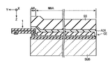
- FIG. 1 is a cross-sectional view showing a sensor according to the first embodiment.
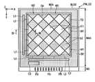
- FIG. 2 is a plan view showing the panel of the sensor.
- FIG. 3 is a cross-sectional view of the panel taken along line III-III in FIG.
- FIG. 4 is an enlarged plan view showing a part of the panel.
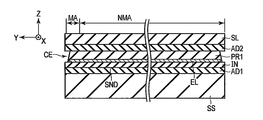
- FIG. 5 is a view for explaining the method for manufacturing the sensor according to the first embodiment, and for explaining a process of forming cells (insulating substrate, element layer, and first protective layer) on the substrate.
- FIG. FIG. 6 is a view for explaining the manufacturing method following FIG. 5, and a cross-sectional view for explaining a process of adhering a support layer to the cell.
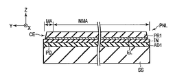
- FIG. 7 is a view for explaining the manufacturing method following FIG.
- FIG. 6 is a cross-sectional view for explaining a state where the substrate is peeled from the cell.
- FIG. 8 is a view for explaining the manufacturing method following FIG. 7, and is a cross-sectional view for explaining a step of bonding a support substrate to the cell.
- FIG. 9 is a view for explaining the manufacturing method following FIG. 8, and is a cross-sectional view for explaining a step of peeling the support layer from the cell.
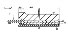
- FIG. 10 is a cross-sectional view showing a sensor according to the second embodiment.
- FIG. 11 is a diagram for explaining the manufacturing method of the sensor according to the second embodiment, and for explaining the process of forming cells (insulating substrate, element layer, and first protective layer) on the substrate.
- FIG. FIG. 12 is a view for explaining the manufacturing method following FIG.
- FIG. 13 is a view for explaining the manufacturing method following FIG. 12, and is a cross-sectional view for explaining a process of bonding a support substrate to the cell and the first wiring board.
- FIG. 14 is a view for explaining the manufacturing method following FIG. 13, and a cross-sectional view for explaining a state where the substrate is peeled from the cell.
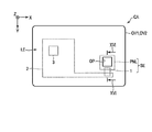
- FIG. 15 is a plan view showing an IC card according to the third embodiment.
- FIG. 16 is a cross-sectional view of the IC card taken along line XVI-XVI in FIG. FIG.
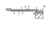
- FIG. 17 is a view for explaining the IC card manufacturing method according to the third embodiment, and is a plan view for explaining a process of fixing the first wiring board to the sensor panel.
- FIG. 18 is a cross-sectional view showing the first wiring board and a part of the panel of FIG.
- FIG. 19 is a view for explaining the manufacturing method following FIG. 17 and FIG. 18, and is a plan view for explaining a step of cutting the first wiring board.
- FIG. 20 is a cross-sectional view showing the first wiring board and a part of the panel of FIG.
- FIG. 21 is a view for explaining the manufacturing method following FIG. 19 and FIG. 20, and is a plan view for explaining a step of pressure-bonding the first wiring board to the second wiring board.
- FIG. 22 is a cross-sectional view showing an IC card according to the fourth embodiment.
- FIG. 23 is a plan view showing a sensor panel according to a modification, and is a view showing a first protective layer and the like.
- FIG. 1 is a cross-sectional view showing a sensor SE according to the first embodiment.
- the first direction X and the second direction Y are orthogonal to each other.
- the third direction Z is orthogonal to the first direction X and the second direction Y, respectively.
- the first direction X and the second direction Y may intersect at an angle other than 90 °.
- the direction toward the tip of the arrow in the third direction Z is defined as up, and the direction opposite to the direction toward the tip of the arrow in the third direction Z is defined as down.
- the second member may be in contact with the first member or separated from the first member. May be located.
- the sensor SE includes a panel PNL and a first wiring board 1.
- the panel PNL includes a cell CE, a support substrate SS, and an adhesive layer AD1.
- the cell CE includes a detection surface SD and a non-detection surface SND opposite to the detection surface.
- the cell CE has a mounting area MA, a non-mounting area NMA, and a linear boundary B between the mounting area MA and the non-mounting area NMA.
- the boundary B extends in the first direction X, for example.
- the cell CE includes an insulating substrate IN, an element layer EL, and a first protective layer PR1.
- the insulating substrate IN is located in the mounting area MA and the non-mounting area NMA.
- the insulating substrate IN is formed using an organic insulating material such as resin.
- the insulating substrate IN is formed using polyimide, for example. For this reason, it may be appropriate to refer to the insulating substrate IN as an organic insulating substrate or a resin substrate. Alternatively, it may be appropriate to refer to the insulating substrate IN as an insulating layer, an organic insulating layer, or a resin layer.
- the insulating substrate IN includes a first surface S1M and a second surface S2M opposite to the first surface.
- the element layer EL is provided on the second surface S2M of the insulating substrate IN.
- the element layer EL is located in the mounting area MA and the non-mounting area NMA.
- the element layer EL includes pads PD and the like located in the mounting area MA.
- the first protective layer PR1 is disposed to face the second surface S2M of the insulating substrate IN. Therefore, the element layer EL is provided between the insulating substrate IN and the first protective layer PR1.
- the first protective layer PR1 is disposed in the non-mounting area NMA and is not disposed in the mounting area MA.
- the first protective layer PR1 covers the element layer EL and is in contact with the element layer EL in the non-mounting region NMA.
- the first protective layer PR1 only needs to be provided so as to expose the pad PD. Therefore, the first protective layer PR1 may be provided in a region where the pad PD is not located in the mounting region MA.
- the detection surface SD of the cell CE is a surface on the side opposite to the surface facing the element layer EL in the first protective layer PR1.
- the non-detection surface SND of the cell CE is the first surface S1M.
- the support substrate SS is formed using an organic insulating material such as resin.
- the support substrate SS is formed using, for example, polyethylene terephthalate (PET).
- PET polyethylene terephthalate
- the support substrate SS may be formed using other resins such as polyethylene naphthalate (PEN). It may be appropriate to refer to the support substrate SS as a support layer, an insulating layer, an organic insulating layer, or a resin layer.
- the adhesive layer AD1 is located between the non-detection surface SND of the cell CE and the support substrate SS.
- the support substrate SS is bonded to the non-detection surface SND of the cell CE by the adhesive layer AD1. Note that the support substrate SS may be adhered to the non-detection surface SND of the cell CE using an adhesive layer instead of the adhesive layer AD1.
- the support substrate SS has a third surface S3M facing the cell CE, and a fourth surface S4M opposite to the third surface.
- the thickness TS of the support substrate SS is larger than any of the thickness TI of the insulating substrate IN and the thickness TP1 of the first protective layer PR1.
- the thickness TI is preferably, for example, 5 ⁇ m or more and 30 ⁇ m or less.
- the thickness TP1 is desirably, for example, 5 ⁇ m or more and 200 ⁇ m or less.
- the thickness TS is desirably 50 ⁇ m or more and 300 ⁇ m or less, for example.
- the numerical value of the thickness described in this specification is an example. Therefore, it does not deny that the numerical value of thickness falls outside the range described in this specification.
- the panel PNL can be formed thick, and the mechanical strength of the panel PNL against stress such as bending can be increased.
- the support substrate SS can increase the mechanical strength of the mounting area MA of the panel PNL.
- the first wiring board 1 is connected to the cell CE.
- the first wiring board 1 is mounted in the mounting area MA of the cell CE.
- the first wiring substrate 1 is electrically connected to the pad PD through an anisotropic conductive film (ACF) 5 that is a conductive material, and is physically fixed to the cell CE.
- ACF anisotropic conductive film
- the first wiring board 1 has a core layer 11, a connection wiring 12, a pad 13, and an insulating layer 14, which are integrally formed.
- the connection wiring 12 is disposed on the core layer 11.
- the connection wiring 12 faces the pad PD of the cell CE and is connected to the pad PD via the anisotropic conductive film 5.
- the pad 13 is located on the side opposite to the connection wiring 12 with respect to the core layer 11.
- the pad 13 is electrically connected to the connection wiring 12 through a through hole formed in the core layer 11.
- the insulating layer 14 covers the connection wiring 12. Therefore, the connection wiring 12 is provided between the core layer 11 and the insulating layer 14.
- the insulating layer 14 exposes at least a portion of the connection wiring 12 connected to the pad PD.
- the pad 13 may be located on the opposite side of the connection wiring 12 with respect to the insulating layer 14.
- the first wiring board 1 has a first end face S1E and a second end face S2E, and extends from the first end face to the second end face. In the present embodiment, the first wiring board 1 extends in the second direction Y.
- the first end face S1E faces the first protective layer PR1 of the cell CE in the second direction Y.
- the connection wiring 12 is exposed at the second end face S2E.
- the second end face S2E of the first wiring board 1 includes the end face of the core layer 11, the end face of the connection wiring 12, and the end face of the insulating layer 14.
- the 1st wiring board 1 should just have the core layer 11 and the connection wiring 12 at least. In that case, the connection wiring 12 may include a portion connected to the pad PD and an alternative portion of the pad 13.
- the core layer 11 and the insulating layer 14 are formed of a resin such as polyimide.
- the first wiring board 1 is a flexible board as a printed board.
- FIG. 2 is a plan view showing a panel PNL of the sensor SE.
- the insulating substrate IN and the support substrate SS have a quadrangular shape.
- the non-mounting area NMA of the cell CE includes a detection area DA and a non-detection area NDA outside the detection area.
- the element layer EL described above includes a plurality of pads PD, a sensor electrode ES, a first circuit C1, a second circuit C2, a third circuit C3, a plurality of wirings L1 and L2, and a shield electrode SH.
- the plurality of pads PD are arranged at intervals in the first direction X in the mounting area MA.
- the sensor electrode ES is located at least in the detection area DA and includes a plurality of first electrodes E1 and a plurality of second electrodes E2.
- Each first wiring W1 includes a plurality of first electrodes E1 arranged in the first direction X.
- Each second wiring W2 includes a plurality of second electrodes E2 arranged in the second direction Y.
- the first circuit C1, the second circuit C2, the third circuit C3, and the shield electrode SH are located in the non-detection area NDA.
- the shield electrode SH covers the first circuit C1, the second circuit C2, and the third circuit C3.
- the second electrode E2 and the shield electrode SH are given a dot pattern.
- Each wiring L1 connects the first electrode E1 on the first circuit C1 side among the plurality of first electrodes E1 to the first circuit C1.
- Each wiring L2 connects the second electrode E2 at the end on the second circuit C2 side among the plurality of second electrodes E2 and the second circuit C2.
- the first circuit C1, the second circuit C2, and the third circuit C3 are connected to a plurality of pads PD via wiring not shown.
- the third circuit C3 includes a timing generator, various logic circuits, and the like.
- the cell CE performs sensing for detecting contact or approach of an object to be detected to the detection surface SD.
- the object to be detected is not particularly limited, and examples thereof include a fingerprint (uneven pattern on the surface of the finger).
- the sensing method of the cell CE of this embodiment is a mutual capacitance method.
- the cell CE can detect contact or approach of an object to be detected based on a change in capacitance between the first wiring W1 and the second wiring W2.
- the first wiring W1 functions as a sensor drive electrode
- the second wiring W2 functions as a detection electrode
- the first circuit C1 functions as a drive circuit and supplies a sensor drive signal to the first wiring W1 via the wiring L1.
- the second wiring W2 is a sensor signal necessary for sensing in accordance with the supply of the sensor driving signal to the first wiring W1, that is, a signal based on a change in capacitance between the first wiring W1 and the second wiring W2. Is output.
- the second circuit C2 functions as a control circuit such as a multiplexer.
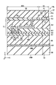
- FIG. 3 is a sectional view showing the panel PNL along the line III-III in FIG.
- the element layer EL in the panel PNL will be described in particular.
- an insulating layer IL1 is provided on the second surface S2M of the insulating substrate IN.
- a semiconductor layer SMC is disposed on the insulating layer IL1.
- the semiconductor layer SMC includes a first region R1, a second region R2, and a channel region RC between the first region R1 and the second region R2.
- One of the first region R1 and the second region R2 functions as a source region, and the other functions as a drain region.
- the semiconductor layer SMC is formed using low-temperature polysilicon.
- the semiconductor layer SMC may be formed of a semiconductor other than polysilicon, such as amorphous silicon or an oxide semiconductor.
- An insulating layer IL2 is provided on the insulating layer IL1 and the semiconductor layer SMC.
- a gate electrode GE is disposed on the insulating layer IL2.
- the gate electrode GE is opposed to at least the channel region RC of the semiconductor layer SMC.
- the gate electrode GE is made of, for example, MoW (molybdenum / tungsten) as a metal material.
- An insulating layer IL3 is provided on the insulating layer IL2 and the gate electrode GE.
- An electrode EA and an electrode EB are disposed on the insulating layer IL3.
- the electrode EA is in contact with the first region R1 through contact holes formed in the insulating layer IL2 and the insulating layer IL3.
- the electrode EB is in contact with the second region R2 through other contact holes formed in the insulating layer IL2 and the insulating layer IL3.
- a part of the electrode EB functions as the wiring L1 shown in FIG.
- the electrode EA and the electrode EB are made of a metal material.
- the electrode EA and the electrode EB each have a three-layer structure (Ti-based / Al-based / Ti-based), and a lower layer made of a metal material mainly composed of Ti such as Ti (titanium) or an alloy containing Ti , Al (aluminum), an intermediate layer made of a metal material mainly containing Al, such as an alloy containing Al, and an upper layer made of a metal material mainly containing Ti, such as an alloy containing Ti or Ti.
- the semiconductor layer SMC, the gate electrode GE, the electrode EA, the electrode EB, etc. constitute a switching element SW.
- the switching element SW is formed of a thin film transistor (TFT) and is included in the first circuit C1 shown in FIG.
- An insulating layer IL4 is provided on the insulating layer IL3, the electrode EA, and the electrode EB.
- a first wiring W1 such as a first electrode E1 is disposed on the insulating layer IL4.
- the first wiring W1 is in contact with the electrode EB through a contact hole formed in the insulating layer IL4. Therefore, the first wiring W1 is electrically connected to the switching element SW (first circuit C1).
- An insulating layer IL5 is provided on the insulating layer IL4 and the first wiring W1.
- the second wiring W2 including the second electrode E2 and the shield electrode SH are disposed on the insulating layer IL5, the second wiring W2 including the second electrode E2 and the shield electrode SH are disposed.
- the second wiring W2 is electrically connected to the switching element (for example, TFT) of the second circuit C2 shown in FIG.
- the wiring L2 is formed in a layer at the same level as the wiring L1.
- the first wiring W1, the second wiring W2, and the shield electrode SH are formed of a transparent conductive material such as indium tin oxide (ITO) or indium zinc oxide (IZO).
- ITO indium tin oxide
- IZO indium zinc oxide
- the first wiring W1, the second wiring W2, and the shield electrode SH are made of ITO.
- the pad PD shown in FIG. 2 has a three-layer stacked structure, and is formed of the lower layer formed of the same material as the electrodes EA and EB and the same material of the first wiring W1. An intermediate layer and an upper layer formed of the same material as the second wiring W2 are included.
- the structure of the pad PD is not limited to the structure of the present embodiment, and various modifications can be made.
- the insulating layers IL1 to IL5 are inorganic insulating layers or organic insulating layers.
- the insulating layers IL1, IL2, IL3, and IL5 are inorganic insulating layers
- the insulating layer IL4 is an organic insulating layer.
- the element layer EL has a laminated structure from the insulating layer IL1 to the second wiring W2 and the shield electrode SH.
- the insulating substrate IN is located on the non-detection surface SND side with respect to the sensor electrode ES
- the first protective layer PR1 is located on the detection surface SD side with respect to the sensor electrode ES.
- the first protective layer PR1 is provided on the insulating layer IL5, the second wiring W2, and the shield electrode SH. Therefore, the shield electrode SH is located between the insulating substrate IN and the first protective layer PR1.
- the switching element SW (first circuit C1) is located between the insulating substrate IN and the shield electrode SH, and is electrically shielded by the shield electrode SH. The same applies to the second circuit C2 and the third circuit C3 shown in FIG. 2, and the second circuit C2 and the third circuit C3 are electrically shielded by the shield electrode SH.
- the shield electrode SH can suppress the leakage of the electric field from the switching element SW (first circuit C1) or the second circuit C2 to the sensor electrode ES. In other words, the shield electrode SH can effectively shield noise generated from the switching element SW (first circuit C1) and the second circuit C2.
- An insulating layer IL4 that is an organic insulating layer is interposed between the shield electrode SH and the electrodes EA and EB.
- the shield electrode SH can be disposed at a distance from the switching element SW. Therefore, it is possible to obtain a shielding effect by the shield electrode SH while suppressing a load of a capacity that can be coupled to the switching element SW by the shield electrode SH.
- the thickness of the insulating layer IL4 is desirably 1 ⁇ m or more and 5 ⁇ m or less, for example.
- the distance from the sensor electrode ES to the detection surface SD is defined as a first distance D1.
- a distance from the sensor electrode ES to the fourth surface S4M is defined as a second distance D2.
- the first distance D1 is a distance from the second wiring W2 to the detection surface SD
- the second distance D2 is a distance from the first wiring W1 to the fourth surface S4M.
- the first distance D1 is shorter than the second distance D2. Since the second distance D2 can be increased compared to the distance from the sensor electrode ES to the detected object, it is difficult to be affected by a capacitance change other than the capacitance change related to the detected object.
- the first wiring W1 and the second wiring W2 can be formed of ITO.
- the light transmittance of the detection area DA can be increased as compared with the case where the switching element is arranged in the detection area DA and the case where the first wiring W1 and the second wiring W2 are formed of metal.
- the sensor SE can be formed on various devices such as a display device.
- FIG. 4 is an enlarged plan view showing a part of the panel PNL.
- the first wiring W1 includes not only the plurality of first electrodes E1 but also a plurality of connection wirings CL1.
- the second wiring W2 includes not only the plurality of second electrodes E2 but also a plurality of connection wirings CL2.
- the plurality of first electrodes E1 are arranged in the first direction X and the second direction Y.
- the first electrode E1 is a square having diagonal lines along the first direction X and the second direction Y, respectively.
- the first electrode E1 has first corners that face each other along the first direction X. In this embodiment, the square first corner of the first electrode E1 is crushed and has a first short side E1S. Therefore, the first electrode E1 is a hexagon having the first short side E1S.
- the connection wiring CL1 connects adjacent first corners (adjacent first short sides E1S).
- connection wiring CL1 is interposed between the insulating layer IL4 and the insulating layer IL5, and is formed integrally with the first electrode E1 using the same material as that of the first electrode E1.
- the plurality of first electrodes E1 and the plurality of connection wirings CL1 connected to each other form a first wiring W1 extending in the first direction X.
- the plurality of first wirings W1 are arranged in the second direction Y.
- the plurality of second electrodes E2 are arranged in the first direction X and the second direction Y with a gap in the first electrode E1.
- the second electrode E2 is a square having diagonal lines along the first direction X and the second direction Y, respectively.
- the second electrode E2 has second corners that face each other along the second direction Y.
- the square second corner of the second electrode E2 is crushed and has a second short side E2S. Therefore, the second electrode E2 is a hexagon having the second short side E2S.
- the connection wiring CL2 connects adjacent second corners (adjacent second short sides E2S).
- connection wiring CL2 is interposed between the insulating layer IL5 and the first protective layer PR1, and is formed integrally with the second electrode E2 using the same material as that of the second electrode E2. In plan view, the connection wiring CL2 intersects with the connection wiring CL1.
- the insulating layer IL5 is interposed between the connection wiring CL1 and the connection wiring CL2.
- the plurality of second electrodes E2 and the plurality of connection wirings CL2 connected to each other form a second wiring W2 extending in the second direction Y.
- the plurality of second wirings W2 are arranged in the first direction X.
- a lattice-shaped slit ST is formed between the first electrode E1 and the second electrode E2.
- the sensor SE is configured as described above.
- a substrate SUB is prepared.
- a glass substrate is used as the substrate SUB.
- a highly heat-resistant polyimide is applied on the substrate SUB.
- the insulating substrate IN is formed on the substrate SUB.
- film formation and patterning are repeated to form an element layer EL on the insulating substrate IN. Therefore, the switching element SW and the like can be formed on the insulating substrate IN having high heat resistance.
- the first protective layer PR1 is formed on the insulating substrate IN and the element layer EL.
- the cell CE is formed on the substrate SUB.
- the support layer SL is attached to the first protective layer PR1 via the adhesive layer AD2.
- a laser is used to irradiate the insulating substrate IN with laser light from the substrate SUB side.
- ablation that absorbs and decomposes the laser light occurs at the interface between the insulating substrate IN and the substrate SUB.
- this creates a space at the interface between the substrate SUB and the insulating substrate IN, and the substrate SUB is peeled from the insulating substrate IN.
- the support substrate SS is attached to the insulating substrate IN via the adhesive layer AD1.
- the support substrate SS is not required to be as heat resistant as the insulating substrate IN, and can therefore be formed using PET or the like.
- the support layer SL and the adhesive layer AD2 are removed from the first protective layer PR1.
- the support layer SL is an indirect material and is discarded in the manufacturing process, it is not used as a part of the final product.
- this forms a panel PNL.
- the portion of the first protective layer PR1 located in the mounting region MA is removed, and the pad PD is exposed.
- the first wiring board 1 is then mounted in the mounting area MA of the cell CE. Thereby, manufacture of sensor SE is completed.
- region MA of the cell CE is not limited to said example.
- the portion of the first protective layer PR1 located in the mounting region MA may be removed to expose the pad PD.
- the support layer SL may be attached to the first protective layer PR1 via the adhesive layer AD2.
- the support layer SL may be attached to the first wiring board 1 via the adhesive layer AD2.
- the sensor SE includes the support substrate SS and the first protective layer PR1 in addition to the cell CE. Therefore, a sensor SE that can increase the mechanical strength can be obtained.
- the thickness TS of the support substrate SS is larger than any of the thickness TI of the insulating substrate IN and the thickness TP1 of the first protective layer PR1.
- the first distance D1 is shorter than the second distance D2. It can be made difficult to be affected by the capacity change other than the capacity change related to the detection object. Therefore, the sensor SE excellent in detection accuracy can be obtained.
- FIG. 10 is a cross-sectional view showing a sensor SE according to the second embodiment.
- the cell CE further includes a second protective layer PR2 located on the detection surface SD side with respect to the insulating substrate IN.
- the first protective layer PR1 is located on the non-detection surface SND side with respect to the sensor electrode ES (element layer EL), and the insulating substrate IN is located on the detection surface SD side with respect to the sensor electrode ES.
- the second protective layer PR2 has a detection surface SD
- the first protective layer PR1 has a non-detection surface SND.
- the first wiring board 1 has a core layer 11, a connection wiring 12, a pad 13, an insulating layer 14, and a pad 15, which are integrally formed.
- the connection wiring 12 is disposed on the core layer 11.
- the pad 13 is located on the side opposite to the connection wiring 12 with respect to the core layer 11.
- the pad 13 is electrically connected to the connection wiring 12 through a through hole formed in the core layer 11.
- the insulating layer 14 covers the connection wiring 12. Therefore, the connection wiring 12 is provided between the core layer 11 and the insulating layer 14.
- the pad 15 is located on the side opposite to the connection wiring 12 with respect to the core layer 11.
- the pad 15 is electrically connected to the connection wiring 12 through a through hole formed in the core layer 11.
- the pad 15 faces the pad PD of the cell CE and is connected to the pad PD via the anisotropic conductive film 5.
- the pad 13 may be located on the opposite side of the connection wiring 12 with respect to the insulating layer 14.
- the first wiring board 1 has a first end face S1E and a second end face S2E, and extends from the first end face to the second end face. In the present embodiment, the first wiring board 1 extends in the second direction Y.
- the first end face S1E faces the first protective layer PR1 of the cell CE in the second direction Y.
- the connection wiring 12 is exposed at the second end face S2E.
- the second end face S2E of the first wiring board 1 includes the end face of the core layer 11, the end face of the connection wiring 12, and the end face of the insulating layer 14.
- the first wiring board 1 only needs to include at least the core layer 11, the connection wiring 12, the pad 13, and the pad 15.
- the mounting area MA of the support substrate SS and the cell CE sandwiches the first wiring board 1 and physically fixes the first wiring board 1.
- the adhesive layer AD1 is also interposed between the support substrate SS and the first wiring substrate 1, and is in contact with the first end surface S1E of the first wiring substrate 1, and the like. Thereby, compared with the case where the mounting area MA of the support substrate SS and the cell CE does not sandwich the first wiring board 1, the portion of the first wiring board 1 that is mounted in the mounting area MA of the cell CE is mechanical. Strength can be increased.
- the thickness TS of the support substrate SS is larger than any of the thickness TI of the insulating substrate IN, the thickness TP1 of the first protective layer PR1, and the thickness TP2 of the second protective layer PR2.
- the thickness TI is preferably, for example, 5 ⁇ m or more and 30 ⁇ m or less.
- the thickness TP1 is desirably, for example, 5 ⁇ m or more and 200 ⁇ m or less.
- the thickness TP2 is preferably 10 ⁇ m or more and 20 ⁇ m or less, for example.
- the thickness TS is desirably 50 ⁇ m or more and 300 ⁇ m or less, for example.
- the panel PNL can be formed thick, and the mechanical strength of the panel PNL against stress such as bending can be increased.
- the support substrate SS can increase the mechanical strength of the mounting area MA of the panel PNL.
- the distance from the sensor electrode ES (element layer EL) to the detection surface SD is defined as a first distance D1.
- a distance from the sensor electrode ES (element layer EL) to the fourth surface S4M is defined as a second distance D2.
- the first distance D1 is shorter than the second distance D2, it can be made difficult to be affected by a capacity change other than the capacity change related to the object to be detected.
- the second protective layer PR2 is formed on the insulating substrate IN side having high mechanical strength in the cell CE, and the second protective layer PR2 has the detection surface SD. Thereby, the mechanical strength of the detection surface SD can be increased.
- the mounting surface of the panel PNL on which the first wiring board 1 is mounted is located on the opposite side of the detection surface SD. Therefore, it is possible to avoid a situation where the first wiring board 1 protrudes from the detection surface SD. Further, the thickness of the sensor SE can be reduced as compared with the sensor SE according to the first embodiment.
- the sensor SE is configured as described above.
- a substrate SUB is prepared.
- a glass substrate is used as the substrate SUB.
- polyimide having high heat resistance is applied on the substrate SUB, and the insulating substrate IN is formed on the substrate SUB.
- film formation and patterning are repeated to form an element layer EL on the insulating substrate IN.
- the first protective layer PR1 is formed on the insulating substrate IN and the element layer EL.
- a portion of the first protective layer PR1 located in the mounting region MA is removed to expose the pad PD.
- the cell CE is formed on the substrate SUB.
- the first wiring board 1 is mounted in the mounting area MA of the cell CE.
- the support substrate SS is attached to the first protective layer PR1 and the first wiring substrate 1 via the adhesive layer AD1. Accordingly, the first wiring board 1 can be sandwiched between the support substrate SS and the mounting area MA of the cell CE.
- a laser is used to irradiate the insulating substrate IN with laser light from the substrate SUB side.
- the substrate SUB is peeled from the insulating substrate IN as shown in FIG.
- the sensor SE being manufactured is inverted so that the insulating substrate IN is located above the support substrate SS, and a second protective layer PR2 is formed on the insulating substrate IN.
- manufacture of sensor SE is completed.
- the mounting area MA of the support substrate SS and the cell CE sandwiches the first wiring board 1, so that the mechanical strength of the sensor SE can be increased. Further, the sensor SE can be thinned.
- FIG. 15 is a plan view showing an IC card CA according to the third embodiment.
- the IC card CA includes an inlet LE and two overlay sheets OV1 and OV2.
- the inlet LE includes a sensor SE including the panel PNL and the first wiring board 1, a second wiring board 2, and a control unit 3.
- the first wiring board 1 is provided independently of the second wiring board 2.
- the second wiring board 2 is connected to the first wiring board 1.
- the control unit 3 is connected to the second wiring board 2.
- the control unit 3 is mounted on the second wiring board 2.
- the control unit 3 is, for example, a central processing unit (CPU).
- the overlay sheets OV1 and OV2 cover both sides of the inlet LE and seal the inlet LE.
- the inlet LE further includes a filler FI.
- the inlet LE and the overlay sheets OV1 and OV2 are welded by, for example, a hot press.
- the sensor SE uses the sensor of the first embodiment.
- the overlay sheet OV1 on the side facing the detection surface SD has an opening OP.
- the opening OP exposes at least the detection area DA in the detection surface SD.
- the filler FI does not exist above the detection surface SD. Therefore, the detected object can be brought into contact with or close to the detection surface SD.
- the pads 13 of the first wiring board 1 are electrically connected to the second wiring board 2 via an anisotropic conductive film 7 that is a conductive material.
- the first wiring board 1 is physically connected to the second wiring board 2. It is fixed to.
- the IC card CA is configured as described above.
- FIGS. 17 and 18 when the manufacture of the IC card CA is started, first, a panel PNL and a first wiring board 1 are prepared, and the first wiring board 1 is mounted on the panel PNL. At this time, the first wiring board 1 extends further in the second direction Y from the first wiring board 1 of the final product shown in FIG. The first wiring board 1 extends in the second direction Y beyond the dividing line DL.
- the insulating layer 14 partially exposes the connection wiring 12 on the side opposite to the first end face S1E of the first wiring board 1.
- the first wiring board 1 (exposed portion of the connection wiring 12) is not shown by extending the first wiring board 1 and partially exposing the connection wiring 12 as described above. It can be connected to the connector of the inspection board. Thereby, before connecting the 1st wiring board 1 to the 2nd wiring board 2, sensor SE, such as panel PNL, can be inspected.
- the sensor SE If the operation of the sensor SE is abnormal, the sensor SE is discarded.
- the first wiring board 1 is cut along the planned dividing line DL. As shown in FIGS. 19 and 20, a small first wiring board 1 can be obtained. Then, the connection wiring 12 is exposed at the second end face S2E of the first wiring board 1 by cutting the first wiring board 1 along the division line DL.
- the first wiring board 1 is then connected to the second wiring board 2.
- the first wiring board 1 can be mounted on the panel PNL before the first wiring board 1 is connected to the second wiring board 2. Therefore, after connecting the 1st wiring board 1 to the 2nd wiring board 2, compared with the case where the 1st wiring board 1 is mounted in panel PNL, the 1st wiring board 1 can be easily mounted in panel PNL. it can. Thereafter, the manufacture of the IC card CA is completed by completing the IC card CA.
- the same effect as in the first embodiment can be obtained.
- FIG. 22 is a sectional view showing an IC card CA according to the fourth embodiment.
- the IC card CA of the present embodiment is configured in the same manner as the IC card of the third embodiment, except that the sensor SE of the second embodiment is used as a sensor SE.
- the same effect as in the third embodiment can be obtained.
- the gap between the overlay sheet OV1 and the detection surface SD can be reduced by the amount of no protrusion of the first wiring board 1 to the detection surface SD side, and the outer surface side of the overlay sheet OV1 can be reduced.
- the distance D3 from the end of the opening OP to the detection surface SD can be further shortened. Thereby, the IC card CA can be thinned.
- the first protective layer PR1 is arranged in the non-mounting area NMA and may not be arranged in the mounting area MA.
- the first protective layer PR1 is hatched. Thereby, when mounting the 1st wiring board 1 in the cell CE, the situation where the 1st wiring board 1 interferes with 1st protective layer PR1 can be avoided.
Landscapes
- Engineering & Computer Science (AREA)
- Theoretical Computer Science (AREA)
- Human Computer Interaction (AREA)
- Physics & Mathematics (AREA)
- General Physics & Mathematics (AREA)
- General Engineering & Computer Science (AREA)
- Multimedia (AREA)
- Microelectronics & Electronic Packaging (AREA)
- Computer Networks & Wireless Communication (AREA)
- Solid State Image Pick-Up Elements (AREA)
- Measurement Of Length, Angles, Or The Like Using Electric Or Magnetic Means (AREA)
- Laminated Bodies (AREA)
- Structure Of Printed Boards (AREA)
Abstract
機械的な強度を高くすることのできるセンサ及びセンサ付き装置を提供する。又は、検出精度に優れたセンサ及びセンサ付き装置を提供する。 センサは、検出面と前記検出面とは反対側の非検出面とを含むセルと、樹脂で形成され前記セルの前記非検出面に接着された支持基板と、を有するパネルを備える。前記セルは、樹脂で形成され第1面と第2面とを含む絶縁基板と、前記絶縁基板の前記第2面に対向配置された第1保護層と、前記絶縁基板と前記第1保護層との間に設けられたセンサ電極と、を有する。前記支持基板の厚みは、前記絶縁基板の厚み、及び前記第1保護層の厚みの何れよりも大きい。
Description
本発明の実施形態は、センサ及びセンサ付き装置に関する。
近年、各種のセンサが開発されている。センサとしては、例えば、指の表面の凹凸パターン(指紋)を検出するセンサが知られている。
本実施形態は、機械的な強度を高くすることのできるセンサ及びセンサ付き装置を提供する。又は、検出精度に優れたセンサ及びセンサ付き装置を提供する。
一実施形態に係るセンサは、
検出面と前記検出面とは反対側の非検出面とを含むセルと、樹脂で形成され前記セルの前記非検出面に接着された支持基板と、を有するパネルを備え、前記セルは、樹脂で形成され第1面と前記第1面とは反対側の第2面とを含む絶縁基板と、前記絶縁基板の前記第2面に対向配置された第1保護層と、前記絶縁基板と前記第1保護層との間に設けられたセンサ電極と、を有し、前記支持基板の厚みは、前記絶縁基板の厚み、及び前記第1保護層の厚みの何れよりも大きい。
検出面と前記検出面とは反対側の非検出面とを含むセルと、樹脂で形成され前記セルの前記非検出面に接着された支持基板と、を有するパネルを備え、前記セルは、樹脂で形成され第1面と前記第1面とは反対側の第2面とを含む絶縁基板と、前記絶縁基板の前記第2面に対向配置された第1保護層と、前記絶縁基板と前記第1保護層との間に設けられたセンサ電極と、を有し、前記支持基板の厚みは、前記絶縁基板の厚み、及び前記第1保護層の厚みの何れよりも大きい。
また、一実施形態に係るセンサ付き装置は、
検出面と前記検出面とは反対側の非検出面とを含むセルと、樹脂で形成され前記セルの前記非検出面に接着された支持基板と、を有するパネルと、前記セルに連結された第1配線基板と、を備えるセンサと、前記第1配線基板に連結された第2配線基板と、前記第2配線基板に連結された制御部と、を備え、前記セルは、樹脂で形成され第1面と前記第1面とは反対側の第2面とを含む絶縁基板と、前記絶縁基板の前記第2面に対向配置された第1保護層と、前記絶縁基板と前記第1保護層との間に設けられたセンサ電極と、を有し、前記第1配線基板は、コア層と、前記コア層に配置された接続配線と、を有し、前記セル側の第1端面から前記第2配線基板側の第2端面まで延在し、前記支持基板の厚みは、前記絶縁基板の厚み、及び前記第1保護層の厚みの何れよりも大きく、前記接続配線は、前記第2端面に露出している。
検出面と前記検出面とは反対側の非検出面とを含むセルと、樹脂で形成され前記セルの前記非検出面に接着された支持基板と、を有するパネルと、前記セルに連結された第1配線基板と、を備えるセンサと、前記第1配線基板に連結された第2配線基板と、前記第2配線基板に連結された制御部と、を備え、前記セルは、樹脂で形成され第1面と前記第1面とは反対側の第2面とを含む絶縁基板と、前記絶縁基板の前記第2面に対向配置された第1保護層と、前記絶縁基板と前記第1保護層との間に設けられたセンサ電極と、を有し、前記第1配線基板は、コア層と、前記コア層に配置された接続配線と、を有し、前記セル側の第1端面から前記第2配線基板側の第2端面まで延在し、前記支持基板の厚みは、前記絶縁基板の厚み、及び前記第1保護層の厚みの何れよりも大きく、前記接続配線は、前記第2端面に露出している。
以下に、本発明の各実施の形態について、図面を参照しつつ説明する。なお、開示はあくまで一例にすぎず、当業者において、発明の主旨を保っての適宜変更について容易に想到し得るものについては、当然に本発明の範囲に含有されるものである。また、図面は説明をより明確にするため、実際の態様に比べ、各部の幅、厚さ、形状等について模式的に表される場合があるが、あくまで一例であって、本発明の解釈を限定するものではない。また、本明細書と各図において、既出の図に関して前述したものと同様の要素には、同一の符号を付して、詳細な説明を適宜省略することがある。
(第1の実施形態)
まず、第1の実施形態に係るセンサSEについて説明する。図1は、第1の実施形態に係るセンサSEを示す断面図である。
図1に示すように、第1方向X及び第2方向Yは互いに直交している。第3方向Zは、第1方向X及び第2方向Yにそれぞれ直交している。なお、本実施形態と異なり、第1方向X及び第2方向Yは、90°以外の角度で交差していてもよい。
本実施形態においては、第3方向Zの矢印の先端に向かう方向を上と定義し、第3方向Zの矢印の先端に向かう方向とは反対側の方向を下と定義する。また、「第1部材の上方の第2部材」及び「第1部材の下方の第2部材」とした場合、第2部材は、第1部材に接していてもよく、又は第1部材から離れて位置していてもよい。
まず、第1の実施形態に係るセンサSEについて説明する。図1は、第1の実施形態に係るセンサSEを示す断面図である。
図1に示すように、第1方向X及び第2方向Yは互いに直交している。第3方向Zは、第1方向X及び第2方向Yにそれぞれ直交している。なお、本実施形態と異なり、第1方向X及び第2方向Yは、90°以外の角度で交差していてもよい。
本実施形態においては、第3方向Zの矢印の先端に向かう方向を上と定義し、第3方向Zの矢印の先端に向かう方向とは反対側の方向を下と定義する。また、「第1部材の上方の第2部材」及び「第1部材の下方の第2部材」とした場合、第2部材は、第1部材に接していてもよく、又は第1部材から離れて位置していてもよい。
センサSEは、パネルPNLと、第1配線基板1と、を備えている。パネルPNLは、セルCEと、支持基板SSと、接着層AD1と、を有している。セルCEは、検出面SDと、上記検出面とは反対側の非検出面SNDと、を含んでいる。セルCEは、実装領域MAと、非実装領域NMAと、実装領域MAと非実装領域NMAとの間の直線状の境界Bと、を有している。境界Bは、例えば第1方向Xに延在している。セルCEは、絶縁基板INと、素子層ELと、第1保護層PR1と、を有している。
絶縁基板INは、実装領域MAと非実装領域NMAとに位置している。絶縁基板INは、樹脂などの有機絶縁材料を用いて形成されている。絶縁基板INは、例えば、ポリイミドを用いて形成されている。このため、絶縁基板INを、有機絶縁基板、又は樹脂基板と称した方が適当な場合があり得る。又は、絶縁基板INを、絶縁層、有機絶縁層、又は樹脂層と称した方が適当な場合があり得る。絶縁基板INは、第1面S1Mと、上記第1面とは反対側の第2面S2Mとを含んでいる。
素子層ELは、絶縁基板INの第2面S2Mの上に設けられている。素子層ELは、実装領域MAと非実装領域NMAとに位置している。素子層ELは、実装領域MAに位置するパッドPDなどを含んでいる。
第1保護層PR1は、絶縁基板INの第2面S2Mに対向配置されている。そのため、素子層ELは、絶縁基板INと第1保護層PR1との間に設けられている。本実施形態において、第1保護層PR1は、非実装領域NMAに配置され、実装領域MAに配置されていない。第1保護層PR1は、非実装領域NMAにて、素子層ELを覆い、素子層ELに接している。なお、第1保護層PR1は、パッドPDを露出させるように設けられていればよい。そのため、第1保護層PR1は、実装領域MAのうちパッドPDが位置していない領域に設けられていてもよい。
本実施形態において、セルCEの検出面SDは、第1保護層PR1のうち素子層ELと対向する面とは反対側の面である。セルCEの非検出面SNDは、第1面S1Mである。
第1保護層PR1は、絶縁基板INの第2面S2Mに対向配置されている。そのため、素子層ELは、絶縁基板INと第1保護層PR1との間に設けられている。本実施形態において、第1保護層PR1は、非実装領域NMAに配置され、実装領域MAに配置されていない。第1保護層PR1は、非実装領域NMAにて、素子層ELを覆い、素子層ELに接している。なお、第1保護層PR1は、パッドPDを露出させるように設けられていればよい。そのため、第1保護層PR1は、実装領域MAのうちパッドPDが位置していない領域に設けられていてもよい。
本実施形態において、セルCEの検出面SDは、第1保護層PR1のうち素子層ELと対向する面とは反対側の面である。セルCEの非検出面SNDは、第1面S1Mである。
支持基板SSは、樹脂などの有機絶縁材料を用いて形成されている。支持基板SSは、例えば、ポリエチレンテレフタレート(PET)を用いて形成されている。但し、支持基板SSは、ポリエチレンナフタレート(PEN)などの他の樹脂を用いて形成されていてもよい。なお、支持基板SSを、支持層、絶縁層、有機絶縁層、又は樹脂層と称した方が適当な場合があり得る。
接着層AD1は、セルCEの非検出面SNDと支持基板SSとの間に位置している。支持基板SSは、接着層AD1によりセルCEの非検出面SNDに接着されている。なお、接着層AD1の替わりに粘着層を利用し、支持基板SSがセルCEの非検出面SNDに粘着されていてもよい。支持基板SSは、セルCEと対向する第3面S3Mと、上記第3面とは反対側の第4面S4Mと、を有している。
支持基板SSの厚みTSは、絶縁基板INの厚みTI、及び第1保護層PR1の厚みTP1の何れよりも大きい。厚みTIは、例えば5μm以上30μm以下であると望ましい。厚みTP1は、例えば5μm以上200μm以下であると望ましい。厚みTSは、例えば50μm以上300μm以下であると望ましい。但し、本明細書に記載した厚みの数値は例示である。よって、厚みの数値が本明細書に記載した範囲外となることを否定するものではない。
支持基板SS及び第1保護層PR1を利用することにより、パネルPNLを厚く形成することができ、曲げなどの応力に対するパネルPNLの機械的強度を高めることができる。例えば、支持基板SSにより、パネルPNLの実装領域MAの機械的強度を高めることができる。
第1配線基板1は、セルCEに連結されている。第1配線基板1は、セルCEの実装領域MAに実装されている。第1配線基板1は、導電材料である異方性導電膜(ACF)5を介してパッドPDに電気的に接続され、セルCEに物理的に固定されている。
第1配線基板1は、コア層11と、接続配線12と、パッド13と、絶縁層14と、を有し、これらが一体となって形成されている。接続配線12は、コア層11に配置されている。接続配線12は、セルCEのパッドPDと対向し、異方性導電膜5を介してパッドPDに接続されている。パッド13は、コア層11に対して接続配線12とは反対側に位置している。パッド13は、コア層11に形成されたスルーホールを通り接続配線12に電気的に接続されている。絶縁層14は、接続配線12を覆っている。そのため、接続配線12は、コア層11と絶縁層14との間に設けられている。なお、絶縁層14は、接続配線12のうち少なくともパッドPDに接続される部分を露出させている。なお、本実施形態と異なり、パッド13は、絶縁層14に対して接続配線12とは反対側に位置していてもよい。
第1配線基板1は、第1端面S1Eと第2端面S2Eとを有し、上記第1端面から上記第2端面まで延在している。本実施形態において、第1配線基板1は第2方向Yに延在している。第1端面S1Eは、セルCEの第1保護層PR1と第2方向Yに対向している。第2端面S2Eにて、接続配線12は露出している。言い換えると、第1配線基板1の第2端面S2Eは、コア層11の端面と、接続配線12の端面と、絶縁層14の端面と、を含んでいる。
なお、第1配線基板1は、少なくとも、コア層11及び接続配線12を有していればよい。その場合、接続配線12は、パッドPDに接続される部分と、上記パッド13の代替部分と、を含んでいればよい。
なお、第1配線基板1は、少なくとも、コア層11及び接続配線12を有していればよい。その場合、接続配線12は、パッドPDに接続される部分と、上記パッド13の代替部分と、を含んでいればよい。
本実施形態の第1配線基板1において、コア層11及び絶縁層14は、ポリイミドなどの樹脂で形成されている。第1配線基板1は、プリント基板としてフレキシブル基板である。
図2は、上記センサSEのパネルPNLを示す平面図である。
図2に示すように、絶縁基板IN及び支持基板SSは、四角形の形状を有している。セルCEの非実装領域NMAは、検出領域DAと、上記検出領域の外側の非検出領域NDAと、を含んでいる。上述した素子層ELは、複数のパッドPD、センサ電極ES、第1回路C1、第2回路C2、第3回路C3、複数の配線L1,L2、及びシールド電極SHを有している。
図2に示すように、絶縁基板IN及び支持基板SSは、四角形の形状を有している。セルCEの非実装領域NMAは、検出領域DAと、上記検出領域の外側の非検出領域NDAと、を含んでいる。上述した素子層ELは、複数のパッドPD、センサ電極ES、第1回路C1、第2回路C2、第3回路C3、複数の配線L1,L2、及びシールド電極SHを有している。
複数のパッドPDは、実装領域MAにて、第1方向Xに間隔を置いて並べられている。センサ電極ESは、少なくとも検出領域DAに位置し、複数の第1電極E1と、複数の第2電極E2と、を有している。各々の第1配線W1は、第1方向Xに並んだ複数の第1電極E1を含んでいる。各々の第2配線W2は、第2方向Yに並んだ複数の第2電極E2を含んでいる。第1回路C1、第2回路C2、第3回路C3、及びシールド電極SHは、非検出領域NDAに位置している。図2の平面視にて、シールド電極SHは、第1回路C1、第2回路C2、及び第3回路C3を覆っている。図中、第2電極E2及びシールド電極SHには、ドットパターンを付している。
各々の配線L1は、複数の第1電極E1のうち第1回路C1側の端の第1電極E1と、第1回路C1と、を接続している。各々の配線L2は、複数の第2電極E2のうち第2回路C2側の端の第2電極E2と、第2回路C2と、を接続している。なお、第1回路C1、第2回路C2、及び第3回路C3は、図示しない配線を介して複数のパッドPDに接続されている。第3回路C3は、タイミングジェネレータ、各種論理回路などを含んでいる。
セルCEは、検出面SDへの被検出物の接触或いは接近を検出するためのセンシングを行うものである。被検出物は、特に限定されるものではないが、例えば指紋(指の表面の凹凸パターン)を挙げることができる。本実施形態のセルCEのセンシング方式は、相互容量方式である。セルCEは、第1配線W1と第2配線W2との間の静電容量の変化に基づいて、被検出物の接触或いは接近を検出することができる。
例えば、第1配線W1がセンサ駆動電極として機能し、第2配線W2が検出電極として機能している。第1回路C1は、駆動回路として機能し、配線L1を介して第1配線W1にセンサ駆動信号を供給する。第2配線W2は、第1配線W1へのセンサ駆動信号の供給にともなって、センシングに必要なセンサ信号、つまり、第1配線W1と第2配線W2との間の容量の変化に基づいた信号を出力する。第2回路C2は、例えばマルチプレクサのような制御回路として機能する。
図3は、上記パネルPNLを図2の線III-IIIに沿って示す断面図である。ここでは、パネルPNLのうち、特に素子層ELについて説明する。
図3に示すように、絶縁基板INの第2面S2Mの上に、絶縁層IL1が設けられている。絶縁層IL1の上に、半導体層SMCが配置されている。半導体層SMCは、第1領域R1と、第2領域R2と、第1領域R1と第2領域R2との間のチャネル領域RCと、を含んでいる。第1領域R1及び第2領域R2のうち、一方がソース領域として機能し、他方がドレイン領域として機能している。本実施形態において、低温ポリシリコンを利用して半導体層SMCが形成されている。但し、半導体層SMCは、アモルファスシリコン、酸化物半導体など、ポリシリコン以外の半導体で形成されていてもよい。
図3に示すように、絶縁基板INの第2面S2Mの上に、絶縁層IL1が設けられている。絶縁層IL1の上に、半導体層SMCが配置されている。半導体層SMCは、第1領域R1と、第2領域R2と、第1領域R1と第2領域R2との間のチャネル領域RCと、を含んでいる。第1領域R1及び第2領域R2のうち、一方がソース領域として機能し、他方がドレイン領域として機能している。本実施形態において、低温ポリシリコンを利用して半導体層SMCが形成されている。但し、半導体層SMCは、アモルファスシリコン、酸化物半導体など、ポリシリコン以外の半導体で形成されていてもよい。
絶縁層IL1及び半導体層SMCの上に、絶縁層IL2が設けられている。絶縁層IL2の上に、ゲート電極GEが配置されている。ゲート電極GEは、少なくとも半導体層SMCのチャネル領域RCと対向している。ゲート電極GEは、金属材料として、例えばMoW(モリブデン・タングステン)で形成されている。
絶縁層IL2及びゲート電極GEの上に、絶縁層IL3が設けられている。絶縁層IL3の上に、電極EA及び電極EBが配置されている。電極EAは、絶縁層IL2及び絶縁層IL3に形成されたコンタクトホールを通り第1領域R1にコンタクトしている。一方、電極EBは、絶縁層IL2及び絶縁層IL3に形成された他のコンタクトホールを通り第2領域R2にコンタクトしている。電極EBの一部は、図2に示した配線L1として機能している。
電極EA及び電極EBは、金属材料で形成されている。例えば、電極EA及び電極EBは、それぞれ3層積層構造(Ti系/Al系/Ti系)が採用され、Ti(チタン)、Tiを含む合金などTiを主成分とする金属材料からなる下層と、Al(アルミニウム)、Alを含む合金などAlを主成分とする金属材料からなる中間層と、Ti、Tiを含む合金などTiを主成分とする金属材料からなる上層と、を有している。
なお、半導体層SMC、ゲート電極GE、電極EA、電極EBなどは、スイッチング素子SWを構成している。スイッチング素子SWは、薄膜トランジスタ(TFT)で形成され、図2に示した第1回路C1に含まれている。
なお、半導体層SMC、ゲート電極GE、電極EA、電極EBなどは、スイッチング素子SWを構成している。スイッチング素子SWは、薄膜トランジスタ(TFT)で形成され、図2に示した第1回路C1に含まれている。
絶縁層IL3、電極EA、及び電極EBの上に、絶縁層IL4が設けられている。絶縁層IL4の上に、第1電極E1などの第1配線W1が配置されている。第1配線W1は、絶縁層IL4に形成されたコンタクトホールを通り、電極EBにコンタクトしている。そのため、第1配線W1は、スイッチング素子SW(第1回路C1)に電気的に接続されている。
絶縁層IL4及び第1配線W1の上に、絶縁層IL5が設けられている。絶縁層IL5の上に、上記第2電極E2を含む第2配線W2、及びシールド電極SHが配置されている。図示しないが、第2配線W2は、図2に示した第2回路C2のスイッチング素子(例えば、TFT)に電気的に接続されている。配線L2は、例えば、配線L1と同一レベルの層に形成されている。
第1配線W1、第2配線W2、及びシールド電極SHは、インジウム・ティン・オキサイド(ITO)やインジウム・ジンク・オキサイド(IZO)等の透明な導電材料によって形成されている。本実施形態において、第1配線W1、第2配線W2、及びシールド電極SHは、ITOで形成されている。
なお、本実施形態において、図2に示したパッドPDは、3層積層構造が採用され、電極EA及び電極EBと同一材料で形成された下層と、第1配線W1と同一材料で形成された中間層と、第2配線W2と同一材料で形成された上層と、を含んでいる。但し、パッドPDの構造は、本実施形態の構造に限定されるものではなく、種々変形可能である。
絶縁層IL1乃至IL5は、無機絶縁層又は有機絶縁層である。本実施形態において、絶縁層IL1,IL2,IL3,IL5は無機絶縁層であり、絶縁層IL4は有機絶縁層である。
上記のことから、素子層ELは、絶縁層IL1から第2配線W2及びシールド電極SHまでの積層構造を有している。セルCEにおいて、絶縁基板INはセンサ電極ESより非検出面SND側に位置し、第1保護層PR1は、センサ電極ESより検出面SD側に位置している。
上記のことから、素子層ELは、絶縁層IL1から第2配線W2及びシールド電極SHまでの積層構造を有している。セルCEにおいて、絶縁基板INはセンサ電極ESより非検出面SND側に位置し、第1保護層PR1は、センサ電極ESより検出面SD側に位置している。
第1保護層PR1は、絶縁層IL5、第2配線W2、及びシールド電極SHの上に設けられている。そのため、シールド電極SHは、絶縁基板INと第1保護層PR1との間に位置している。スイッチング素子SW(第1回路C1)は、絶縁基板INとシールド電極SHとの間に位置し、シールド電極SHにより電気的にシールドされている。なお、図2に示した第2回路C2、及び第3回路C3に関しても同様であり、第2回路C2、及び第3回路C3は、シールド電極SHにより電気的にシールドされている。
また、シールド電極SHは、スイッチング素子SW(第1回路C1)や第2回路C2からセンサ電極ESへの電界の漏れを抑制することができる。言い換えると、シールド電極SHは、スイッチング素子SW(第1回路C1)や第2回路C2から発生するノイズを効果的に遮蔽することができる。シールド電極SHと電極EA,EBとの間には、有機絶縁層である絶縁層IL4が介在している。スイッチング素子SWに距離を置いてシールド電極SHを配置することができる。そのため、シールド電極SHによりスイッチング素子SWに結合され得る容量の負荷を抑制しつつ、シールド電極SHによるシールド効果を得ることができる。なお、絶縁層IL4の厚みは、例えば1μm以上5μm以下であると望ましい。
ここで、センサ電極ESから検出面SDまでの距離を第1距離D1とする。センサ電極ESから第4面S4Mまでの距離を第2距離D2とする。本実施形態において、第1距離D1は第2配線W2から検出面SDまでの距離であり、第2距離D2は第1配線W1から第4面S4Mまでの距離である。第1距離D1は、第2距離D2より短い。センサ電極ESから被検出物までの距離と比較して、第2距離D2を長くすることができるため、被検出物に関する容量変化以外の容量変化の影響を受け難くすることができる。
本実施形態において、検出領域DAにスイッチング素子SWなどのスイッチング素子を配置する必要が無い。第1配線W1、及び第2配線W2をITOで形成することが可能である。検出領域DAにスイッチング素子を配置する場合や、第1配線W1、及び第2配線W2を金属で形成する場合と比較して、検出領域DAの光透過率を高めることができる。これにより、表示装置などの各種デバイスの上にセンサSEを形成することが可能となる。
図4は、パネルPNLの一部を示す拡大平面図である。
図4、並びに図2及び図3に示すように、第1配線W1は、複数の第1電極E1だけではなく複数の接続配線CL1も含んでいる。第2配線W2は、複数の第2電極E2だけではなく複数の接続配線CL2も含んでいる。
図4、並びに図2及び図3に示すように、第1配線W1は、複数の第1電極E1だけではなく複数の接続配線CL1も含んでいる。第2配線W2は、複数の第2電極E2だけではなく複数の接続配線CL2も含んでいる。
複数の第1電極E1は、第1方向X及び第2方向Yに並べられている。第1電極E1は、それぞれ第1方向X及び第2方向Yに沿った対角線を持つ正方形である。第1電極E1は、第1方向Xに沿って対向し合う第1角部を有している。この実施形態において、第1電極E1の正方形の第1角部は潰れ第1短辺E1Sを有している。このため、第1電極E1は、第1短辺E1Sを有した六角形である。第1方向Xにおいて、接続配線CL1は、隣合う第1角部同士(隣合う第1短辺E1S同士)を接続している。
接続配線CL1は、絶縁層IL4と絶縁層IL5との間に介在し、第1電極E1の材料と同一の材料を利用し、第1電極E1と一体に形成されている。互いに接続された複数の第1電極E1及び複数の接続配線CL1は、第1方向Xに延在した第1配線W1を形成している。複数の第1配線W1は、第2方向Yに並べられている。
平面視にて、複数の第2電極E2は、第1電極E1に隙間を置いて第1方向X及び第2方向Yに並べられている。第2電極E2は、それぞれ第1方向X及び第2方向Yに沿った対角線を持つ正方形である。第2電極E2は、第2方向Yに沿って対向し合う第2角部を有している。この実施形態において、第2電極E2の正方形の第2角部は潰れ第2短辺E2Sを有している。このため、第2電極E2は、第2短辺E2Sを有した六角形である。第2方向Yにおいて、接続配線CL2は、隣合う第2角部同士(隣合う第2短辺E2S同士)を接続している。
接続配線CL2は、絶縁層IL5と第1保護層PR1との間に介在し、第2電極E2の材料と同一の材料を利用し、第2電極E2と一体に形成されている。平面視にて、接続配線CL2は、接続配線CL1と交差している。絶縁層IL5は、接続配線CL1と接続配線CL2との間に介在している。互いに接続された複数の第2電極E2及び複数の接続配線CL2は、第2方向Yに延在した第2配線W2を形成している。複数の第2配線W2は、第1方向Xに並べられている。
平面視にて、第1電極E1及び第2電極E2間に、格子状のスリットSTが形成されている。
センサSEは上述したように構成されている。
センサSEは上述したように構成されている。
次に、上記センサSEの製造方法について説明する。
図5に示すように、センサSEの製造が開始されると、まず、基板SUBを用意する。本実施形態において、基板SUBとしてガラス基板を利用している。続いて、基板SUBの上に、耐熱性の高いポリイミドを塗布する。これにより、基板SUBの上に絶縁基板INが形成される。次いで、成膜及びパターニングを繰り返し、絶縁基板INの上に素子層ELを形成する。そのため、耐熱性の高い絶縁基板INの上に、上記スイッチング素子SWなどを形成することができる。その後、絶縁基板IN及び素子層ELの上に、第1保護層PR1を形成する。これにより、基板SUBの上に、セルCEが形成される。
図5に示すように、センサSEの製造が開始されると、まず、基板SUBを用意する。本実施形態において、基板SUBとしてガラス基板を利用している。続いて、基板SUBの上に、耐熱性の高いポリイミドを塗布する。これにより、基板SUBの上に絶縁基板INが形成される。次いで、成膜及びパターニングを繰り返し、絶縁基板INの上に素子層ELを形成する。そのため、耐熱性の高い絶縁基板INの上に、上記スイッチング素子SWなどを形成することができる。その後、絶縁基板IN及び素子層ELの上に、第1保護層PR1を形成する。これにより、基板SUBの上に、セルCEが形成される。
図6に示すように、続いて、接着層AD2を介して支持層SLを第1保護層PR1に張り付ける。次いで、レーザを用い、基板SUB側から絶縁基板INにレーザ光を照射する。レーザ光が絶縁基板INに到達すると、絶縁基板INと基板SUBとの間の界面で、レーザ光を吸収して分解するアブレーションを生じる。
図7に示すように、これにより、基板SUB及び絶縁基板INの界面に空間が生じ、絶縁基板INから基板SUBが剥離される。
図7に示すように、これにより、基板SUB及び絶縁基板INの界面に空間が生じ、絶縁基板INから基板SUBが剥離される。
図8に示すように、その後、接着層AD1を介して支持基板SSを絶縁基板INに張り付ける。これにより、セルCEの非検出面SNDにフレキシブルな厚い支持基板SSを設けることが可能である。なお、支持基板SSは、絶縁基板INほどの耐熱性を要求されるものではないため、PETなどを用いて形成可能である。続いて、支持層SL及び接着層AD2を、第1保護層PR1から除去する。ここで、上記支持層SLは間接材料であり、上記の製造工程にて破棄されるため、最終製品の一部としては使用されない。
図9に示すように、これにより、パネルPNLが形成される。次いで、第1保護層PR1のうち実装領域MAに位置する部分を除去し、パッドPDを露出させる。
図1に示しように、その後、第1配線基板1をセルCEの実装領域MAに実装する。これにより、センサSEの製造が終了する。
図9に示すように、これにより、パネルPNLが形成される。次いで、第1保護層PR1のうち実装領域MAに位置する部分を除去し、パッドPDを露出させる。
図1に示しように、その後、第1配線基板1をセルCEの実装領域MAに実装する。これにより、センサSEの製造が終了する。
なお、第1配線基板1をセルCEの実装領域MAに実装するタイミングは、上記の例に限定されるものではない。例えば、図5において、基板SUBの上にセルCEを形成した後、第1保護層PR1のうち実装領域MAに位置する部分を除去し、パッドPDを露出させてもよい。そして、第1配線基板1をセルCEの実装領域MAに実装した後、接着層AD2を介して支持層SLを第1保護層PR1に張り付けてもよい。その際、第1配線基板1にも、接着層AD2を介して支持層SLを張り付けてもよい。
上記のように構成された第1の実施形態によれば、センサSEは、セルCE以外に、支持基板SS及び第1保護層PR1を備えている。そのため、機械的な強度を高くすることのできるセンサSEを得ることができる。
支持基板SSの厚みTSは、絶縁基板INの厚みTI、及び第1保護層PR1の厚みTP1の何れよりも大きい。そして、第1距離D1は、第2距離D2より短い。被検出物に関する容量変化以外の容量変化の影響を受け難くすることができる。そのため、検出精度に優れたセンサSEを得ることができる。
支持基板SSの厚みTSは、絶縁基板INの厚みTI、及び第1保護層PR1の厚みTP1の何れよりも大きい。そして、第1距離D1は、第2距離D2より短い。被検出物に関する容量変化以外の容量変化の影響を受け難くすることができる。そのため、検出精度に優れたセンサSEを得ることができる。
(第2の実施形態)
次に、第2の実施形態に係るセンサSEについて説明する。第2の実施形態に係るセンサSEは、後述する点以外、上記第1の実施形態と同様に構成されている。図10は、第2の実施形態に係るセンサSEを示す断面図である。
図10に示すように、セルCEは、絶縁基板INより検出面SD側に位置している第2保護層PR2をさらに有している。セルCEにおいて、第1保護層PR1は上記センサ電極ES(素子層EL)より非検出面SND側に位置し、絶縁基板INは上記センサ電極ESより検出面SD側に位置している。本実施形態において、第2保護層PR2は検出面SDを有し、第1保護層PR1は非検出面SNDを有している。
次に、第2の実施形態に係るセンサSEについて説明する。第2の実施形態に係るセンサSEは、後述する点以外、上記第1の実施形態と同様に構成されている。図10は、第2の実施形態に係るセンサSEを示す断面図である。
図10に示すように、セルCEは、絶縁基板INより検出面SD側に位置している第2保護層PR2をさらに有している。セルCEにおいて、第1保護層PR1は上記センサ電極ES(素子層EL)より非検出面SND側に位置し、絶縁基板INは上記センサ電極ESより検出面SD側に位置している。本実施形態において、第2保護層PR2は検出面SDを有し、第1保護層PR1は非検出面SNDを有している。
第1配線基板1は、コア層11と、接続配線12と、パッド13と、絶縁層14と、パッド15と、を有し、これらが一体となって形成されている。接続配線12は、コア層11に配置されている。パッド13は、コア層11に対して接続配線12とは反対側に位置している。パッド13は、コア層11に形成されたスルーホールを通り接続配線12に電気的に接続されている。絶縁層14は、接続配線12を覆っている。そのため、接続配線12は、コア層11と絶縁層14との間に設けられている。
パッド15は、コア層11に対して接続配線12とは反対側に位置している。パッド15は、コア層11に形成されたスルーホールを通り接続配線12に電気的に接続されている。パッド15は、セルCEのパッドPDと対向し、異方性導電膜5を介してパッドPDに接続されている。なお、本実施形態と異なり、パッド13は、絶縁層14に対して接続配線12とは反対側に位置していてもよい。
第1配線基板1は、第1端面S1Eと第2端面S2Eとを有し、上記第1端面から上記第2端面まで延在している。本実施形態において、第1配線基板1は第2方向Yに延在している。第1端面S1Eは、セルCEの第1保護層PR1と第2方向Yに対向している。第2端面S2Eにて、接続配線12は露出している。言い換えると、第1配線基板1の第2端面S2Eは、コア層11の端面と、接続配線12の端面と、絶縁層14の端面と、を含んでいる。
なお、第1配線基板1は、少なくとも、コア層11、接続配線12、パッド13、及びパッド15を有していればよい。
なお、第1配線基板1は、少なくとも、コア層11、接続配線12、パッド13、及びパッド15を有していればよい。
支持基板SS及びセルCEの実装領域MAは、第1配線基板1を挟み、第1配線基板1を物理的に固定している。接着層AD1は、支持基板SSと第1配線基板1との間にも介在し、第1配線基板1の第1端面S1Eなどに接している。これにより、支持基板SS及びセルCEの実装領域MAが第1配線基板1を挟んでいない場合と比較し、第1配線基板1のうちセルCEの実装領域MAに実装される部分の機械的な強度を高めることができる。
支持基板SSの厚みTSは、絶縁基板INの厚みTI、第1保護層PR1の厚みTP1、及び第2保護層PR2の厚みTP2の何れよりも大きい。厚みTIは、例えば5μm以上30μm以下であると望ましい。厚みTP1は、例えば5μm以上200μm以下であると望ましい。厚みTP2は、例えば10μm以上20μm以下であると望ましい。厚みTSは、例えば50μm以上300μm以下であると望ましい。
支持基板SS、第1保護層PR1、及び第2保護層PR2を利用することにより、パネルPNLを厚く形成することができ、曲げなどの応力に対するパネルPNLの機械的強度を高めることができる。例えば、支持基板SSにより、パネルPNLの実装領域MAの機械的強度を高めることができる。
ここで、センサ電極ES(素子層EL)から検出面SDまでの距離を第1距離D1とする。センサ電極ES(素子層EL)から第4面S4Mまでの距離を第2距離D2とする。本実施形態においても、第1距離D1は、第2距離D2より短いため、被検出物に関する容量変化以外の容量変化の影響を受け難くすることができる。
第2保護層PR2は、セルCEのうち機械的強度の高い絶縁基板IN側に形成され、第2保護層PR2に検出面SDを持たせている。これにより、検出面SDの機械的強度を高めることができる。
第1配線基板1が実装されるパネルPNLの実装面は、検出面SDの反対側に位置している。そのため、第1配線基板1が検出面SDに出っ張る事態を回避することができる。また、第1の実施形態に係るセンサSEと比較し、センサSEの厚みを小さくすることができる。
第1配線基板1が実装されるパネルPNLの実装面は、検出面SDの反対側に位置している。そのため、第1配線基板1が検出面SDに出っ張る事態を回避することができる。また、第1の実施形態に係るセンサSEと比較し、センサSEの厚みを小さくすることができる。
センサSEは上述したように構成されている。
次に、上記センサSEの製造方法について説明する。
図11に示すように、センサSEの製造が開始されると、まず、基板SUBを用意する。本実施形態において、基板SUBとしてガラス基板を利用している。続いて、基板SUBの上に耐熱性の高いポリイミドを塗布し、基板SUBの上に絶縁基板INを形成する。次いで、成膜及びパターニングを繰り返し、絶縁基板INの上に素子層ELを形成する。その後、絶縁基板IN及び素子層ELの上に、第1保護層PR1を形成する。なお、その際、第1保護層PR1のうち実装領域MAに位置する部分を除去し、パッドPDを露出させている。これにより、基板SUBの上に、セルCEが形成される。
図11に示すように、センサSEの製造が開始されると、まず、基板SUBを用意する。本実施形態において、基板SUBとしてガラス基板を利用している。続いて、基板SUBの上に耐熱性の高いポリイミドを塗布し、基板SUBの上に絶縁基板INを形成する。次いで、成膜及びパターニングを繰り返し、絶縁基板INの上に素子層ELを形成する。その後、絶縁基板IN及び素子層ELの上に、第1保護層PR1を形成する。なお、その際、第1保護層PR1のうち実装領域MAに位置する部分を除去し、パッドPDを露出させている。これにより、基板SUBの上に、セルCEが形成される。
図12に示すように、続いて、第1配線基板1を、セルCEの実装領域MAに実装する。
図13に示すように、次いで、接着層AD1を介して支持基板SSを第1保護層PR1及び第1配線基板1に張り付ける。これにより、第1配線基板1を、支持基板SSとセルCEの実装領域MAとで挟むことができる。
その後、レーザを用い、基板SUB側から絶縁基板INにレーザ光を照射する。
図13に示すように、次いで、接着層AD1を介して支持基板SSを第1保護層PR1及び第1配線基板1に張り付ける。これにより、第1配線基板1を、支持基板SSとセルCEの実装領域MAとで挟むことができる。
その後、レーザを用い、基板SUB側から絶縁基板INにレーザ光を照射する。
図14に示すように、これにより、絶縁基板INから基板SUBが剥離される。
図10に示すように、その後、支持基板SSより絶縁基板INが上側となるように製造途中のセンサSEを反転し、絶縁基板INの上に、第2保護層PR2を形成する。これにより、センサSEの製造が終了する。
上記のように構成された第2の実施形態においても、上記第1の実施形態と同様の効果を得ることができる。第2の実施形態では、支持基板SS及びセルCEの実装領域MAは、第1配線基板1を挟んでいるため、センサSEの機械的な強度を高めることができる。また、センサSEの薄型化を図ることができる。
図10に示すように、その後、支持基板SSより絶縁基板INが上側となるように製造途中のセンサSEを反転し、絶縁基板INの上に、第2保護層PR2を形成する。これにより、センサSEの製造が終了する。
上記のように構成された第2の実施形態においても、上記第1の実施形態と同様の効果を得ることができる。第2の実施形態では、支持基板SS及びセルCEの実装領域MAは、第1配線基板1を挟んでいるため、センサSEの機械的な強度を高めることができる。また、センサSEの薄型化を図ることができる。
(第3の実施形態)
次に、第3の実施形態に係るセンサ付き装置について説明する。ここでは、センサ付き装置としてICカードCAを例に説明する。但し、本実施形態と異なり、センサ付き装置はICカード以外のデバイスに適用可能である。図15は、第3の実施形態に係るICカードCAを示す平面図である。
次に、第3の実施形態に係るセンサ付き装置について説明する。ここでは、センサ付き装置としてICカードCAを例に説明する。但し、本実施形態と異なり、センサ付き装置はICカード以外のデバイスに適用可能である。図15は、第3の実施形態に係るICカードCAを示す平面図である。
図15に示すように、ICカードCAは、インレットLEと、2枚のオーバレイシートOV1,OV2と、を備えている。インレットLEは、パネルPNL及び第1配線基板1を備えるセンサSEと、第2配線基板2と、制御部3と、を具備している。第1配線基板1は、第2配線基板2から独立して設けられている。第2配線基板2は、第1配線基板1に連結されている。制御部3は、第2配線基板2に連結されている。本実施形態において、制御部3は、第2配線基板2に実装されている。制御部3は、例えば、中央演算処理装置(CPU)である。オーバレイシートOV1,OV2は、インレットLEの両面を覆い、インレットLEを封止している。
図16は、ICカードCAを図15の線XVI-XVIに沿って示す断面図である。
図16及び図15に示すように、インレットLEは、充填材FIをさらに含んでいる。インレットLE及びオーバレイシートOV1,OV2は、例えば、熱プレスなどにより溶着されている。センサSEは、上記第1の実施形態のセンサを用いている。
図16及び図15に示すように、インレットLEは、充填材FIをさらに含んでいる。インレットLE及びオーバレイシートOV1,OV2は、例えば、熱プレスなどにより溶着されている。センサSEは、上記第1の実施形態のセンサを用いている。
検出面SDと対向する側のオーバレイシートOV1は、開口OPを有している。開口OPは、検出面SDのうち、少なくとも検出領域DAを露出させている。なお、開口OPと対向する領域において、検出面SDの上方に充填材FIは存在していない。そのため、検出面SDに被検出物を接触或いは接近させることができる。第1配線基板1のパッド13は、導電材料である異方性導電膜7を介して第2配線基板2に電気的に接続され、第1配線基板1は、第2配線基板2に物理的に固定されている。
ICカードCAは、上記のように構成されている。
ICカードCAは、上記のように構成されている。
次に、ICカードCAの製造方法について説明する。特に、センサSEの検査方法について説明する。
図17及び図18に示すように、ICカードCAの製造が開始されると、まず、パネルPNLと第1配線基板1とを用意し、パネルPNLに第1配線基板1を実装する。この時点で、第1配線基板1は、図15に示した最終製品の第1配線基板1より第2方向Yに、一層、延出している。第1配線基板1は、分断予定線DLを越えて第2方向Yに延出している。
図17及び図18に示すように、ICカードCAの製造が開始されると、まず、パネルPNLと第1配線基板1とを用意し、パネルPNLに第1配線基板1を実装する。この時点で、第1配線基板1は、図15に示した最終製品の第1配線基板1より第2方向Yに、一層、延出している。第1配線基板1は、分断予定線DLを越えて第2方向Yに延出している。
第1配線基板1の第1端面S1Eとは反対側にて、絶縁層14は接続配線12を部分的に露出させている。上記のように、第1配線基板1を延出させ、かつ、接続配線12を上記のように部分的に露出させることで、第1配線基板1(接続配線12の露出部分)を、図示しない検査ボードのコネクタに接続させることができる。これにより、第1配線基板1を第2配線基板2に連結する前に、パネルPNLなどのセンサSEを検査することができる。
センサSEの動作が異常であった場合、センサSEを廃棄する。
センサSEの動作が正常であった場合、第1配線基板1を分断予定線DLに沿って切断する。
図19及び図20に示すように、これにより、小型の第1配線基板1を得ることができる。そして、第1配線基板1を分断予定線DLに沿って切断することで、第1配線基板1の第2端面S2Eにて、接続配線12は露出している。
センサSEの動作が正常であった場合、第1配線基板1を分断予定線DLに沿って切断する。
図19及び図20に示すように、これにより、小型の第1配線基板1を得ることができる。そして、第1配線基板1を分断予定線DLに沿って切断することで、第1配線基板1の第2端面S2Eにて、接続配線12は露出している。
図21及び図16に示すように、その後、第1配線基板1を第2配線基板2に連結する。上記のように、本実施形態では、第1配線基板1を第2配線基板2に連結する前に、第1配線基板1をパネルPNLに実装することができる。そのため、第1配線基板1を第2配線基板2に連結した後に、第1配線基板1をパネルPNLに実装する場合と比較して、第1配線基板1をパネルPNLに容易に実装することができる。
以降、ICカードCAを完成させることで、ICカードCAの製造が終了する。
以降、ICカードCAを完成させることで、ICカードCAの製造が終了する。
上記のように構成された第3の実施形態においても、上記第1の実施形態と同様の効果を得ることができる。第3の実施形態では、パネルPNLへの第1配線基板1の実装が容易である。また、ICカードCAを完成させる前に、センサSEを検査することができる。
(第4の実施形態)
次に、第4の実施形態に係るセンサ付き装置について説明する。ここでも、センサ付き装置としてICカードCAを例に説明する。図22は、第4の実施形態に係るICカードCAを示す断面図である。
図22に示すように、本実施形態のICカードCAは、センサSEとして上記第2の実施形態のセンサを用いている以外、上記第3の実施形態のICカードと同様に構成されている。
次に、第4の実施形態に係るセンサ付き装置について説明する。ここでも、センサ付き装置としてICカードCAを例に説明する。図22は、第4の実施形態に係るICカードCAを示す断面図である。
図22に示すように、本実施形態のICカードCAは、センサSEとして上記第2の実施形態のセンサを用いている以外、上記第3の実施形態のICカードと同様に構成されている。
上記のように構成された第4の実施形態においても、上記第3の実施形態と同様の効果を得ることができる。第4の実施形態では、検出面SD側への第1配線基板1の出っ張りが無い分、オーバレイシートOV1と検出面SDとの間の隙間を小さくすることができ、オーバレイシートOV1の外面側における開口OPの端から検出面SDまでの距離D3を、一層、短くすることができる。これにより、ICカードCAの薄型化を図ることができる。
本発明のいくつかの実施形態を説明したが、これらの実施形態は、例として提示したものであり、発明の範囲を限定することは意図していない。これら新規な実施形態は、その他の様々な形態で実施されることが可能であり、発明の要旨を逸脱しない範囲で、種々の省略、置き換え、変更を行うことができる。これら実施形態やその変形は、発明の範囲や要旨に含まれるとともに、特許請求の範囲に記載された発明とその均等の範囲に含まれる。必要に応じて、複数の実施形態を組合せることも可能である。
例えば、図23に示すように、第1保護層PR1は、非実装領域NMAに配置され、実装領域MAに配置されていなくともよい。図中、第1保護層PR1には斜線を付している。これにより、第1配線基板1をセルCEに実装する際、第1配線基板1が第1保護層PR1に干渉する事態を回避することができる。
Claims (20)
- 検出面と前記検出面とは反対側の非検出面とを含むセルと、樹脂で形成され前記セルの前記非検出面に接着された支持基板と、を有するパネルを備え、
前記セルは、樹脂で形成され第1面と前記第1面とは反対側の第2面とを含む絶縁基板と、前記絶縁基板の前記第2面に対向配置された第1保護層と、前記絶縁基板と前記第1保護層との間に設けられたセンサ電極と、を有し、
前記支持基板の厚みは、前記絶縁基板の厚み、及び前記第1保護層の厚みの何れよりも大きい、
センサ。 - 前記支持基板は、前記セルと対向する第3面と、前記第3面とは反対側の第4面と、を有し、
前記センサ電極から前記検出面までの第1距離は、前記センサ電極から前記第4面までの第2距離より短い、
請求項1に記載のセンサ。 - 第1配線基板をさらに備え、
前記セルは、実装領域と、非実装領域と、前記実装領域と前記非実装領域との間の直線状の境界と、を有し、
前記第1保護層は、前記非実装領域に配置され、前記実装領域に配置されておらず、
前記第1配線基板は、前記第1保護層と対向した第1端面を有し、前記セルの前記実装領域に実装されている、
請求項1に記載のセンサ。 - 前記第1配線基板は、コア層と、前記コア層に配置された接続配線と、を有し、前記第1端面から第2端面まで延在し、
前記接続配線は、前記第2端面に露出している、
請求項3に記載のセンサ。 - 前記セルにおいて、
前記絶縁基板は、前記センサ電極より前記非検出面側に位置し、
前記第1保護層は、前記センサ電極より前記検出面側に位置している、
請求項1に記載のセンサ。 - 前記セルにおいて、
前記第1保護層は、前記センサ電極より前記非検出面側に位置し、
前記絶縁基板は、前記センサ電極より前記検出面側に位置している、
請求項1に記載のセンサ。 - 前記セルは、前記絶縁基板より前記検出面側に位置している第2保護層をさらに有する、
請求項6に記載のセンサ。 - 第1配線基板をさらに備え、
前記セルは、実装領域と、非実装領域と、前記実装領域と前記非実装領域との間の直線状の境界と、を有し、
前記第1保護層は、前記非実装領域に配置され、前記実装領域に配置されておらず、
前記第1配線基板は、前記第1保護層と対向した第1端面を有し、前記セルの前記実装領域に実装され、
前記支持基板及び前記セルの前記実装領域は、前記第1配線基板を挟み、前記第1配線基板を物理的に固定している、
請求項6に記載のセンサ。 - 第1配線基板をさらに備え、
前記セルは、前記第1配線基板が実装される実装領域と、非実装領域と、前記センサ電極に電気的に接続されたスイッチング素子を含む回路と、前記絶縁基板と前記第1保護層との間に位置したシールド電極と、を有し、
前記非実装領域は、検出領域と、前記検出領域の外側の非検出領域と、を含み、
前記センサ電極は、前記検出領域に位置し、
前記回路及び前記シールド電極は、前記非検出領域に位置し、
前記回路は、前記絶縁基板と前記シールド電極との間に位置し、前記シールド電極により電気的にシールドされている、
請求項1に記載のセンサ。 - 前記センサ電極は、透明な導電材料で形成されている、
請求項1に記載のセンサ。 - 前記支持基板は、ポリエチレンテレフタレート又はポリエチレンナフタレートで形成され、
前記絶縁基板は、ポリイミドで形成されている、
請求項1に記載のセンサ。 - 前記絶縁基板の厚みは、5μm以上30μm以下であり、
前記第1保護層の厚みは、5μm以上200μm以下であり、
前記支持基板の厚みは、300μm以下である、
請求項1に記載のセンサ。 - 検出面と前記検出面とは反対側の非検出面とを含むセルと、樹脂で形成され前記セルの前記非検出面に接着された支持基板と、を有するパネルと、前記セルに連結された第1配線基板と、を備えるセンサと、
前記第1配線基板に連結された第2配線基板と、
前記第2配線基板に連結された制御部と、を備え、
前記セルは、樹脂で形成され第1面と前記第1面とは反対側の第2面とを含む絶縁基板と、前記絶縁基板の前記第2面に対向配置された第1保護層と、前記絶縁基板と前記第1保護層との間に設けられたセンサ電極と、を有し、
前記第1配線基板は、コア層と、前記コア層に配置された接続配線と、を有し、前記セル側の第1端面から前記第2配線基板側の第2端面まで延在し、
前記支持基板の厚みは、前記絶縁基板の厚み、及び前記第1保護層の厚みの何れよりも大きく、
前記接続配線は、前記第2端面に露出している、
センサ付き装置。 - 前記支持基板は、前記セルと対向する第3面と、前記第3面とは反対側の第4面と、を有し、
前記センサ電極から前記検出面までの第1距離は、前記センサ電極から前記第4面までの第2距離より短い、
請求項13に記載のセンサ付き装置。 - 前記セルは、実装領域と、非実装領域と、前記実装領域と前記非実装領域との間の直線状の境界と、を有し、
前記第1保護層は、前記非実装領域に配置され、前記実装領域に配置されておらず、
前記第1配線基板は、前記第1保護層と対向した第1端面を有し、前記セルの前記実装領域に実装されている、
請求項13に記載のセンサ付き装置。 - 前記セルにおいて、
前記絶縁基板は、前記センサ電極より前記非検出面側に位置し、
前記第1保護層は、前記センサ電極より前記検出面側に位置している、
請求項13に記載のセンサ付き装置。 - 前記セルにおいて、
前記第1保護層は、前記センサ電極より前記非検出面側に位置し、
前記絶縁基板は、前記センサ電極より前記検出面側に位置している、
請求項13に記載のセンサ付き装置。 - 前記セルは、前記第1配線基板が実装される実装領域と、非実装領域と、前記センサ電極に電気的に接続されたスイッチング素子を含む回路と、前記絶縁基板と前記第1保護層との間に位置したシールド電極と、を有し、
前記非実装領域は、検出領域と、前記検出領域の外側の非検出領域と、を含み、
前記センサ電極は、前記検出領域に位置し、
前記回路及び前記シールド電極は、前記非検出領域に位置し、
前記回路は、前記絶縁基板と前記シールド電極との間に位置し、前記シールド電極により電気的にシールドされている、
請求項13に記載のセンサ付き装置。 - 前記センサ電極は、透明な導電材料で形成されている、
請求項13に記載のセンサ付き装置。 - 前記支持基板は、ポリエチレンテレフタレート又はポリエチレンナフタレートで形成され、
前記絶縁基板は、ポリイミドで形成されている、
請求項13に記載のセンサ付き装置。
Priority Applications (1)
| Application Number | Priority Date | Filing Date | Title |
|---|---|---|---|
| US17/108,677 US11430250B2 (en) | 2018-06-01 | 2020-12-01 | Sensor and sensor-equipped device |
Applications Claiming Priority (2)
| Application Number | Priority Date | Filing Date | Title |
|---|---|---|---|
| JP2018-106156 | 2018-06-01 | ||
| JP2018106156A JP2019211906A (ja) | 2018-06-01 | 2018-06-01 | センサ及びセンサ付き装置 |
Related Child Applications (1)
| Application Number | Title | Priority Date | Filing Date |
|---|---|---|---|
| US17/108,677 Continuation US11430250B2 (en) | 2018-06-01 | 2020-12-01 | Sensor and sensor-equipped device |
Publications (1)
| Publication Number | Publication Date |
|---|---|
| WO2019230615A1 true WO2019230615A1 (ja) | 2019-12-05 |
Family
ID=68696960
Family Applications (1)
| Application Number | Title | Priority Date | Filing Date |
|---|---|---|---|
| PCT/JP2019/020780 Ceased WO2019230615A1 (ja) | 2018-06-01 | 2019-05-24 | センサ及びセンサ付き装置 |
Country Status (3)
| Country | Link |
|---|---|
| US (1) | US11430250B2 (ja) |
| JP (1) | JP2019211906A (ja) |
| WO (1) | WO2019230615A1 (ja) |
Families Citing this family (1)
| Publication number | Priority date | Publication date | Assignee | Title |
|---|---|---|---|---|
| KR20210094194A (ko) * | 2020-01-20 | 2021-07-29 | 삼성디스플레이 주식회사 | 전자패널 및 이를 포함한 표시장치 |
Citations (5)
| Publication number | Priority date | Publication date | Assignee | Title |
|---|---|---|---|---|
| JP2012003768A (ja) * | 2010-06-18 | 2012-01-05 | Sutech Trading Ltd | タッチ式透明キーボード |
| JP2013152561A (ja) * | 2012-01-24 | 2013-08-08 | Japan Display West Co Ltd | タッチパネル、表示装置および電子機器 |
| JP2014056461A (ja) * | 2012-09-13 | 2014-03-27 | Wonder Future Corp | タッチパネルの製造方法及びタッチパネル、並びにタッチパネルと表示装置を具備する入出力一体型装置 |
| JP2014531679A (ja) * | 2011-09-30 | 2014-11-27 | カナトゥ オイ | 接触検知膜、接触検知装置及び電子装置 |
| JP2015114801A (ja) * | 2013-12-11 | 2015-06-22 | シャープ株式会社 | 表示装置及びアンロック方法 |
Family Cites Families (7)
| Publication number | Priority date | Publication date | Assignee | Title |
|---|---|---|---|---|
| CA1026237A (en) * | 1973-09-17 | 1978-02-14 | Kureha Kagaku Kogyo Kabushiki Kaisha | Key board switch |
| JPH0659270A (ja) * | 1992-08-10 | 1994-03-04 | Hitachi Ltd | 液晶表示装置 |
| JPH07191339A (ja) * | 1993-12-27 | 1995-07-28 | Hitachi Ltd | 液晶表示装置 |
| JP5033078B2 (ja) * | 2008-08-06 | 2012-09-26 | 株式会社ジャパンディスプレイイースト | 表示装置 |
| KR20140074740A (ko) * | 2012-12-10 | 2014-06-18 | 삼성디스플레이 주식회사 | 디스플레이 장치 및 그의 제조방법 |
| US10203816B2 (en) | 2013-05-07 | 2019-02-12 | Egis Technology Inc. | Apparatus and method for TFT fingerprint sensor |
| CN104978559B (zh) | 2014-04-03 | 2018-05-25 | 神盾股份有限公司 | 薄膜晶体管指纹传感器及其操作方法 |
-
2018
- 2018-06-01 JP JP2018106156A patent/JP2019211906A/ja active Pending
-
2019
- 2019-05-24 WO PCT/JP2019/020780 patent/WO2019230615A1/ja not_active Ceased
-
2020
- 2020-12-01 US US17/108,677 patent/US11430250B2/en active Active
Patent Citations (5)
| Publication number | Priority date | Publication date | Assignee | Title |
|---|---|---|---|---|
| JP2012003768A (ja) * | 2010-06-18 | 2012-01-05 | Sutech Trading Ltd | タッチ式透明キーボード |
| JP2014531679A (ja) * | 2011-09-30 | 2014-11-27 | カナトゥ オイ | 接触検知膜、接触検知装置及び電子装置 |
| JP2013152561A (ja) * | 2012-01-24 | 2013-08-08 | Japan Display West Co Ltd | タッチパネル、表示装置および電子機器 |
| JP2014056461A (ja) * | 2012-09-13 | 2014-03-27 | Wonder Future Corp | タッチパネルの製造方法及びタッチパネル、並びにタッチパネルと表示装置を具備する入出力一体型装置 |
| JP2015114801A (ja) * | 2013-12-11 | 2015-06-22 | シャープ株式会社 | 表示装置及びアンロック方法 |
Also Published As
| Publication number | Publication date |
|---|---|
| US11430250B2 (en) | 2022-08-30 |
| US20210081637A1 (en) | 2021-03-18 |
| JP2019211906A (ja) | 2019-12-12 |
Similar Documents
| Publication | Publication Date | Title |
|---|---|---|
| CN110246865B (zh) | 显示设备 | |
| US10088950B2 (en) | Display device with touch panel having X, Y and dummy electrodes | |
| CN111354765B (zh) | 柔性显示装置 | |
| CN107799550B (zh) | 柔性显示器 | |
| CN107819006B (zh) | 显示装置 | |
| CN106992197B (zh) | 柔性显示器及其制造方法 | |
| US8890830B2 (en) | Display device-integrated touch screen panel | |
| JP5377279B2 (ja) | 静電容量型入力装置および入力機能付き電気光学装置 | |
| CN102053766B (zh) | 静电电容型输入装置、制造方法及带输入功能的电光设备 | |
| US10318031B2 (en) | Display apparatus integrated with a touch screen panel and including a guard ring pattern | |
| US20110298750A1 (en) | Touch-sensitive device and fabrication method thereof and touch-sensitive display device | |
| TWI549031B (zh) | 觸控面板與觸控顯示裝置 | |
| KR20180047586A (ko) | 인-셀 터치 폴더블 표시 장치 | |
| KR20200047933A (ko) | 표시 장치 | |
| CN102799295A (zh) | 触控装置及触控显示装置 | |
| JP7529455B2 (ja) | 検出装置 | |
| CN109979907B (zh) | 电子产品 | |
| KR20220105218A (ko) | 표시 장치 | |
| KR101991892B1 (ko) | 테이프 패키지 및 이를 구비한 평판 표시 장치 | |
| WO2020258872A1 (zh) | 触摸感应装置、触控显示面板及触控显示面板母板 | |
| WO2019230615A1 (ja) | センサ及びセンサ付き装置 | |
| CN117093089A (zh) | 具有触摸传感器的显示装置 | |
| KR102709948B1 (ko) | 터치 센서 적층체 및 이의 제조 방법 | |
| KR20240112110A (ko) | 지문센서 기판 및 이를 포함하는 지문센서 패키지 | |
| KR101960055B1 (ko) | 터치 센서 및 표시 장치 |
Legal Events
| Date | Code | Title | Description |
|---|---|---|---|
| 121 | Ep: the epo has been informed by wipo that ep was designated in this application |
Ref document number: 19811744 Country of ref document: EP Kind code of ref document: A1 |
|
| NENP | Non-entry into the national phase |
Ref country code: DE |
|
| 122 | Ep: pct application non-entry in european phase |
Ref document number: 19811744 Country of ref document: EP Kind code of ref document: A1 |