WO2019227939A1 - 移位寄存器单元、电路结构、栅极驱动电路、驱动电路及显示装置 - Google Patents
移位寄存器单元、电路结构、栅极驱动电路、驱动电路及显示装置 Download PDFInfo
- Publication number
- WO2019227939A1 WO2019227939A1 PCT/CN2019/070895 CN2019070895W WO2019227939A1 WO 2019227939 A1 WO2019227939 A1 WO 2019227939A1 CN 2019070895 W CN2019070895 W CN 2019070895W WO 2019227939 A1 WO2019227939 A1 WO 2019227939A1
- Authority
- WO
- WIPO (PCT)
- Prior art keywords
- conductive portion
- connection conductive
- transistor
- circuit
- signal
- Prior art date
Links
Images


Classifications
-
- G—PHYSICS
- G09—EDUCATION; CRYPTOGRAPHY; DISPLAY; ADVERTISING; SEALS
- G09G—ARRANGEMENTS OR CIRCUITS FOR CONTROL OF INDICATING DEVICES USING STATIC MEANS TO PRESENT VARIABLE INFORMATION
- G09G3/00—Control arrangements or circuits, of interest only in connection with visual indicators other than cathode-ray tubes
- G09G3/20—Control arrangements or circuits, of interest only in connection with visual indicators other than cathode-ray tubes for presentation of an assembly of a number of characters, e.g. a page, by composing the assembly by combination of individual elements arranged in a matrix no fixed position being assigned to or needed to be assigned to the individual characters or partial characters
- G09G3/22—Control arrangements or circuits, of interest only in connection with visual indicators other than cathode-ray tubes for presentation of an assembly of a number of characters, e.g. a page, by composing the assembly by combination of individual elements arranged in a matrix no fixed position being assigned to or needed to be assigned to the individual characters or partial characters using controlled light sources
- G09G3/30—Control arrangements or circuits, of interest only in connection with visual indicators other than cathode-ray tubes for presentation of an assembly of a number of characters, e.g. a page, by composing the assembly by combination of individual elements arranged in a matrix no fixed position being assigned to or needed to be assigned to the individual characters or partial characters using controlled light sources using electroluminescent panels
- G09G3/32—Control arrangements or circuits, of interest only in connection with visual indicators other than cathode-ray tubes for presentation of an assembly of a number of characters, e.g. a page, by composing the assembly by combination of individual elements arranged in a matrix no fixed position being assigned to or needed to be assigned to the individual characters or partial characters using controlled light sources using electroluminescent panels semiconductive, e.g. using light-emitting diodes [LED]
- G09G3/3208—Control arrangements or circuits, of interest only in connection with visual indicators other than cathode-ray tubes for presentation of an assembly of a number of characters, e.g. a page, by composing the assembly by combination of individual elements arranged in a matrix no fixed position being assigned to or needed to be assigned to the individual characters or partial characters using controlled light sources using electroluminescent panels semiconductive, e.g. using light-emitting diodes [LED] organic, e.g. using organic light-emitting diodes [OLED]
- G09G3/3266—Details of drivers for scan electrodes
-
- G—PHYSICS
- G09—EDUCATION; CRYPTOGRAPHY; DISPLAY; ADVERTISING; SEALS
- G09G—ARRANGEMENTS OR CIRCUITS FOR CONTROL OF INDICATING DEVICES USING STATIC MEANS TO PRESENT VARIABLE INFORMATION
- G09G3/00—Control arrangements or circuits, of interest only in connection with visual indicators other than cathode-ray tubes
- G09G3/007—Use of pixel shift techniques, e.g. by mechanical shift of the physical pixels or by optical shift of the perceived pixels
-
- G—PHYSICS
- G09—EDUCATION; CRYPTOGRAPHY; DISPLAY; ADVERTISING; SEALS
- G09G—ARRANGEMENTS OR CIRCUITS FOR CONTROL OF INDICATING DEVICES USING STATIC MEANS TO PRESENT VARIABLE INFORMATION
- G09G3/00—Control arrangements or circuits, of interest only in connection with visual indicators other than cathode-ray tubes
- G09G3/20—Control arrangements or circuits, of interest only in connection with visual indicators other than cathode-ray tubes for presentation of an assembly of a number of characters, e.g. a page, by composing the assembly by combination of individual elements arranged in a matrix no fixed position being assigned to or needed to be assigned to the individual characters or partial characters
- G09G3/2092—Details of a display terminals using a flat panel, the details relating to the control arrangement of the display terminal and to the interfaces thereto
-
- G—PHYSICS
- G09—EDUCATION; CRYPTOGRAPHY; DISPLAY; ADVERTISING; SEALS
- G09G—ARRANGEMENTS OR CIRCUITS FOR CONTROL OF INDICATING DEVICES USING STATIC MEANS TO PRESENT VARIABLE INFORMATION
- G09G3/00—Control arrangements or circuits, of interest only in connection with visual indicators other than cathode-ray tubes
- G09G3/20—Control arrangements or circuits, of interest only in connection with visual indicators other than cathode-ray tubes for presentation of an assembly of a number of characters, e.g. a page, by composing the assembly by combination of individual elements arranged in a matrix no fixed position being assigned to or needed to be assigned to the individual characters or partial characters
- G09G3/34—Control arrangements or circuits, of interest only in connection with visual indicators other than cathode-ray tubes for presentation of an assembly of a number of characters, e.g. a page, by composing the assembly by combination of individual elements arranged in a matrix no fixed position being assigned to or needed to be assigned to the individual characters or partial characters by control of light from an independent source
- G09G3/36—Control arrangements or circuits, of interest only in connection with visual indicators other than cathode-ray tubes for presentation of an assembly of a number of characters, e.g. a page, by composing the assembly by combination of individual elements arranged in a matrix no fixed position being assigned to or needed to be assigned to the individual characters or partial characters by control of light from an independent source using liquid crystals
- G09G3/3611—Control of matrices with row and column drivers
- G09G3/3674—Details of drivers for scan electrodes
-
- G—PHYSICS
- G11—INFORMATION STORAGE
- G11C—STATIC STORES
- G11C19/00—Digital stores in which the information is moved stepwise, e.g. shift registers
- G11C19/28—Digital stores in which the information is moved stepwise, e.g. shift registers using semiconductor elements
-
- G—PHYSICS
- G09—EDUCATION; CRYPTOGRAPHY; DISPLAY; ADVERTISING; SEALS
- G09G—ARRANGEMENTS OR CIRCUITS FOR CONTROL OF INDICATING DEVICES USING STATIC MEANS TO PRESENT VARIABLE INFORMATION
- G09G2300/00—Aspects of the constitution of display devices
- G09G2300/04—Structural and physical details of display devices
- G09G2300/0421—Structural details of the set of electrodes
- G09G2300/0426—Layout of electrodes and connections
-
- G—PHYSICS
- G09—EDUCATION; CRYPTOGRAPHY; DISPLAY; ADVERTISING; SEALS
- G09G—ARRANGEMENTS OR CIRCUITS FOR CONTROL OF INDICATING DEVICES USING STATIC MEANS TO PRESENT VARIABLE INFORMATION
- G09G2310/00—Command of the display device
- G09G2310/02—Addressing, scanning or driving the display screen or processing steps related thereto
- G09G2310/0243—Details of the generation of driving signals
- G09G2310/0245—Clearing or presetting the whole screen independently of waveforms, e.g. on power-on
-
- G—PHYSICS
- G09—EDUCATION; CRYPTOGRAPHY; DISPLAY; ADVERTISING; SEALS
- G09G—ARRANGEMENTS OR CIRCUITS FOR CONTROL OF INDICATING DEVICES USING STATIC MEANS TO PRESENT VARIABLE INFORMATION
- G09G2310/00—Command of the display device
- G09G2310/02—Addressing, scanning or driving the display screen or processing steps related thereto
- G09G2310/0264—Details of driving circuits
- G09G2310/0286—Details of a shift registers arranged for use in a driving circuit
-
- G—PHYSICS
- G09—EDUCATION; CRYPTOGRAPHY; DISPLAY; ADVERTISING; SEALS
- G09G—ARRANGEMENTS OR CIRCUITS FOR CONTROL OF INDICATING DEVICES USING STATIC MEANS TO PRESENT VARIABLE INFORMATION
- G09G2310/00—Command of the display device
- G09G2310/06—Details of flat display driving waveforms
- G09G2310/061—Details of flat display driving waveforms for resetting or blanking
Definitions
- Embodiments of the present disclosure relate to a shift register unit, a circuit structure, a gate driving circuit, a driving circuit, and a display device.
- a pixel array of a display panel generally includes a plurality of rows of gate lines and a plurality of columns of data lines interlaced therewith.
- the gate line can be driven by an integrated driving circuit.
- the gate driving circuit can also be directly integrated on the thin film transistor array substrate to form a GOA (Gate Driver On Array) to drive the gate lines.
- GOA Gate Driver On Array
- a GOA circuit composed of a plurality of cascaded shift register units may be used to provide switching state voltage signals to multiple rows of gate lines of a pixel array, thereby controlling the multiple rows of gate lines to sequentially turn on.
- At least one embodiment of the present disclosure provides a shift register unit, which can flexibly select a position for connecting conductive parts according to the distance between the transistors, and avoids that the connecting conductive parts connected to each transistor are provided on the same layer, thereby simplifying the display panel. Routing design and improve the accuracy of signal transmission.
- At least one embodiment of the present disclosure provides a shift register unit, which includes a base substrate and an input circuit, a reset circuit, and a first output circuit, a first output terminal, a first output terminal, and the input circuit disposed on the base substrate.
- the input circuit is configured to control a level of a first node in response to an input signal; the reset circuit is configured to reset the first node in response to a reset signal; and the first output circuit is configured to Under the control of the level of the first node, outputting a first signal to the first output terminal; in the first connection conductive portion, the second connection conductive portion, and the third connection conductive portion Of any two or three different layers.
- the shift register unit provided by an embodiment of the present disclosure further includes a first signal line input terminal and a fourth connection conductive portion.
- the fourth connection conductive portion connects the first output circuit and the first signal line input terminal, and is configured to be connected to the first connection conductive portion, the second connection conductive portion, and the third connection. Any two or three different layers of the conductive portion are provided.
- the shift register unit provided by an embodiment of the present disclosure further includes an output noise reduction circuit and a fifth connection conductive portion.
- the output noise reduction circuit is configured to perform noise reduction on the first output terminal under the control of the level of the second node; the fifth connection conductive part connects the output noise reduction circuit and the first
- the output circuit is configured to be disposed in a different layer from any two or three of the first connection conductive portion, the second connection conductive portion, and the third connection conductive portion.
- the shift register unit provided by an embodiment of the present disclosure further includes a control circuit, a second signal line input terminal, and a sixth connection conductive portion.
- the control circuit is configured to control the level of the second node under the control of the level of the first node and / or the second signal; the sixth connection conductive portion is configured to connect to the The control circuit and the second signal line input end are arranged in different layers from the fourth connection conductive portion.
- a length of the first connection conductive portion is shorter than a length of the second connection conductive portion; or the first signal includes a clock signal, a voltage signal, At least one of a current signal; or the second signal includes at least one of a clock signal, a voltage signal, and a current signal.
- At least one embodiment of the present disclosure further provides a circuit structure including a base substrate, a first transistor, a second transistor, a third transistor, and a storage capacitor, a first output terminal, and a first connection disposed on the base substrate.
- the first connection conductive portion is configured to connect a first pole of the first transistor and a first electrode of the second transistor; and the second connection conductive portion is configured to connect a first pole of the second transistor.
- the third connection conductive portion is configured to connect the first output terminal and the first electrode of the third transistor; the Any two or three of the first connection conductive portion, the second connection conductive portion, and the third connection conductive portion are disposed in different layers.
- the circuit structure provided by an embodiment of the present disclosure further includes a fourth transistor, a first signal line input terminal, a fourth connection conductive portion, and a fifth connection conductive portion.
- the fourth connection conductive portion is configured to connect the second pole of the third transistor and the first signal line input terminal, and is connected to the first connection conductive portion, the second connection conductive portion, and the first connection line. Any two or three different layers of the third connection conductive portion are provided; the fifth connection conductive portion is configured to connect the first pole of the third transistor and the first pole of the fourth transistor, and Any two or three of the first connection conductive portion, the second connection conductive portion, and the third connection conductive portion are disposed in different layers.
- the circuit structure provided by an embodiment of the present disclosure further includes a fifth transistor, a sixth transistor, a second signal line input terminal, and a sixth connection conductive portion.
- the first pole of the fifth transistor is connected to the first pole of the sixth transistor through the first connection conductive portion; the sixth connection conductive portion is configured to connect the gate of the sixth transistor and the gate of the sixth transistor.
- the second signal line input terminal is disposed in a different layer from the fourth connection conductive portion.
- the first pole of the third transistor is disposed on the same layer as the second connection conductive portion; or the first connection conductive portion and the first transistor
- the semiconductor layer is made of the same material.
- the circuit structure provided by an embodiment of the present disclosure further includes a seventh transistor, a third signal line input terminal, and a seventh connection conductive portion.
- the gate of the seventh transistor is configured to be connected to the first output terminal to receive an output signal of the circuit structure, and the first pole of the seventh transistor is configured to be connected to the conductive portion through the seventh connection.
- An input terminal of the third signal line is connected to receive a third signal, and a second pole of the seventh transistor is configured to be connected to a second output terminal.
- all The seventh connection conductive portion is configured to be disposed at a different layer from the fourth connection conductive portion.
- a circuit structure provided by an embodiment of the present disclosure further includes an eighth transistor; a gate of the eighth transistor is configured to be connected to a second node through the second connection conductive portion, and the first One pole is configured to be connected to the second output terminal, and the second pole of the eighth transistor is configured to be connected to a first voltage terminal to receive a first voltage.
- At least one embodiment of the present disclosure provides a gate driving circuit including a plurality of cascaded shift register units provided by any one of the embodiments of the present disclosure.
- the gate driving circuit further includes a second output circuit, a third signal line input terminal, and a seventh connection conductive portion.
- the second output circuit is configured to output a third signal to the second output terminal under the control of the level output from the first output terminal; when the shift register unit includes a fourth connection conductive portion
- the seventh connection conductive portion is configured to connect the third signal line input terminal and the second output circuit, and is disposed at a different layer from the fourth connection conductive portion.
- At least one embodiment of the present disclosure also provides a driving circuit including a plurality of cascaded circuit structures provided by any one of the embodiments of the present disclosure.
- At least one embodiment of the present disclosure provides a display device including a gate driving circuit or a driving circuit provided by any one of the embodiments of the present disclosure, and the gate driving circuit or the driving circuit is disposed on four sides of an array substrate.
- a display device further includes a first conductive layer, a second conductive layer, a third conductive layer, a fourth conductive layer, a fifth conductive layer, and a sixth conductive layer.
- the first conductive layer Same material as the active layer
- the second conductive layer is the same as the first gate line layer
- the third conductive layer is the same as the second gate line layer
- the fourth conductive layer is the same as the first data line layer
- the fifth conductive layer is made of the same material as the second data line layer
- the sixth conductive layer is made of the same material as the pixel electrode.
- FIG. 1 is a schematic diagram of an example of a shift register unit according to an embodiment of the present disclosure
- FIG. 2 is a schematic diagram of another example of a shift register unit according to an embodiment of the present disclosure.
- FIG. 3 is a circuit diagram of an implementation example of the shift register unit shown in FIG. 1; FIG.
- 4A is a schematic cross-sectional structure diagram of an example of an array substrate taken along line A1-A2 in FIG. 3;
- 4B is a schematic cross-sectional structure view of the array substrate taken along the line C1-C2 in FIG. 3;
- 4C is a schematic cross-sectional structure view of the array substrate taken along line D1-D2 in FIG. 3;
- 4D is a schematic cross-sectional structure diagram of a conductive layer where each connection conductive portion is provided according to an embodiment of the present disclosure
- FIG. 5 is a schematic circuit diagram of an implementation example of the shift register unit shown in FIG. 2; FIG.
- FIG. 6 is a schematic diagram of still another example of a shift register unit according to an embodiment of the present disclosure.
- FIG. 7 is a circuit diagram of an implementation example of the shift register unit shown in FIG. 6; FIG.
- FIG. 8 is a circuit diagram of another implementation example of the shift register unit shown in FIG. 6; FIG.
- 9A is a schematic diagram of an example of a gate driving circuit according to an embodiment of the present disclosure.
- 9B is a schematic diagram of another example of a gate driving circuit according to an embodiment of the present disclosure.
- 9C is a schematic diagram of still another example of a gate driving circuit according to an embodiment of the present disclosure.
- FIG. 10A is a schematic block diagram of a gate driving circuit shown in FIG. 9B or 9C;
- FIG. 10B is a circuit diagram of an implementation example of the gate driving circuit shown in FIG. 10A;
- FIG. 11A is a signal timing chart corresponding to the operation of the gate driving circuit shown in FIG. 9B;
- FIG. 11B is a signal timing chart corresponding to the operation of the gate driving circuit shown in FIG. 9C.
- FIG. 12 is a schematic diagram of a display device according to an embodiment of the present disclosure.
- GOA Gate Driver On Array
- the gate drive circuit is integrated on the display panel through a thin film transistor process, so that narrow bezels and reduced assembly costs can be achieved.
- At least one embodiment of the present disclosure provides a shift register unit including a base substrate and an input circuit, a reset circuit and a first output circuit, a first output terminal, a first output terminal, and a first circuit connected to the input circuit and the reset circuit.
- the input circuit is configured to control the level of the first node in response to the input signal; the reset circuit is configured to reset the first node in response to the reset signal; the first output circuit is configured to be at the level of the first node Under control, the first signal is output to the first output terminal; any two or three of the first connection conductive portion, the second connection conductive portion, and the third connection conductive portion are arranged in different layers.
- At least one embodiment of the present disclosure also provides a circuit structure, a gate driving circuit, and a display device.
- the shift register unit provided in the embodiment of the present disclosure can flexibly select a position for connecting the conductive parts according to the distance between the transistors, thereby avoiding that multiple connection conductive parts connected to each transistor are provided on the same layer, thereby simplifying the wiring of the display panel Design and improve the accuracy of signal transmission.
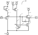
- FIG. 1 is a schematic block diagram of an example of a shift register unit according to an embodiment of the present disclosure.
- the shift register unit 100 includes a base substrate (not shown in FIG. 1) and an input circuit 110, a reset circuit 120, a first output circuit 130, and a first output terminal provided on the base substrate. OUT1.
- the shift register unit 100 is formed as a constituent unit of a gate driving circuit on an array substrate of a display device.
- the array substrate includes the above-mentioned base substrate, and has an array region (display region) and a peripheral region.
- the gate driving circuit is formed in a peripheral region of the array substrate, and the pixel circuit is formed in an array region of the array substrate.
- the pixel circuit may include at least one transistor, such as a switching transistor, and may further include components such as a driving transistor.
- the thin film transistor in the array region and the thin film transistor in the peripheral region can be obtained through a semiconductor fabrication process.
- the shift register unit 100 further includes a first connection conductive portion 1 connecting the input circuit 110 and the reset circuit 120, a second connection conductive portion 2 connecting the reset circuit 120 and the first output circuit 130, and a first connection conductive portion 2.
- An output circuit 130 is connected to the third conductive portion 3 of the first output terminal OUT1.
- the third connection conductive portion 3 may be integrated with the gate line of the array substrate in the array area, or the third connection conductive portion 3 may be electrically connected to the gate line of the array substrate in the array area through a via, a connection line, or the like .
- the first connection conductive portion 1, the second connection conductive portion 2, and the third connection conductive portion 3 are disposed on a base substrate, and any two or three of them are disposed in different layers.
- the first connection conductive portion 1 and the second connection conductive portion 2 are disposed in different layers, and the third connection conductive portion 3 may be disposed in the same layer or a different layer from any of the first connection conductive portion 1 and the second connection conductive portion 2.
- the first connection conductive portion 1, the second connection conductive portion 2, and the third connection conductive portion 3 are all disposed on different layers, which are not limited in the embodiments of the present disclosure.
- the embodiments of the present disclosure are not limited to the number and connection manner of the first connection conductive portion 1, the second connection conductive portion 2, and the third connection conductive portion 3.
- the first connection conductive portion 1 indicates that there is at least one first connection conductive portion 1 for electrical connection between the input circuit 110 and the reset circuit 120, and the number and manner of connection are not limited; that is, there is at least one input circuit
- the connection conductive parts in the following embodiments are the same, and will not be described again.
- the length of the first connection conductive portion is smaller than the length of the second connection conductive portion.
- the length indicates the extension distance from the beginning to the end of the connection conductive portion, or the extension distance between the vias at the junction of the transistor elements in the circuit, so that the connection to the conductive portion can be flexibly selected according to the extension distance between the transistors. s position.
- the extension distance depends on the shape (for example, line shape, S shape, etc.) of the connection conductive portion, rather than a straight line distance between the two ends.
- the input circuit 110 is configured to control a level of a first node (not shown in FIG. 1, see FIG. 3) in response to an input signal, for example, to charge the first node.
- the first node is a meeting point of the first connection conductive portion 1 and the second connection conductive portion 2, and belongs to both the first connection conductive portion 1 and the second connection conductive portion 2, and does not indicate an actually existing component.
- the input circuit 110 may be respectively connected to the input terminal INPUT and the first connection conductive part 1 (ie, the first node), and is configured to transmit the voltage signal received by the input circuit 110 to the first node.
- the reset circuit 120 is configured to reset the first node in response to a reset signal.
- the reset circuit 120 may be configured to be connected to the reset terminal RST, the first connection conductive portion 1 (that is, the first node), and the second connection conductive portion 2 (that is, the first node), so that the reset terminal RST can be input.
- the first node Under the control of the reset signal, the first node is applied with a low-level signal or is electrically connected to a low voltage terminal.
- the low voltage terminal is, for example, the first voltage terminal VGL or a reference voltage terminal, so that the first node can be pulled down and reset. .
- the embodiment of the present disclosure is described by taking an N-type transistor as an example. It should be noted that the embodiments of the present disclosure are not limited thereto, and a circuit structure of a P-type or mixed N-type and P-type transistor may also be adopted, and only the corresponding transistor needs to be Just turn on the low level.
- controlling the level of a node includes charging the node to raise the level of the node, or Discharge the node to pull the node down.
- Charging a node means, for example, electrically connecting the node with a high-level voltage signal, so that the high-level voltage signal is used to raise the level of the node;
- discharging a node means, for example, connecting the node with A low-level voltage signal is electrically connected, so that the low-level voltage signal is used to pull down the level of the node.
- a capacitor electrically connected to the node may be provided, and charging or discharging the node means charging or discharging the capacitor electrically connected to the node.
- the high level and the low level are relative.
- the high level indicates a higher voltage range (for example, the high level can be 5V, 10V, or other suitable voltages), and multiple high levels can be the same or different.
- the low level indicates a lower voltage range (for example, the low level may adopt 0V, -5V, -10V, or other suitable voltages), and multiple low levels may be the same or different.
- the minimum value of the high level is greater than the maximum value of the low level.
- the first output circuit 130 is configured to output a first signal to the first output terminal OUT1 under the control of the level of the first node.
- the first signal may include a first clock signal or other voltage signals (for example, High level signal).
- the first output circuit 130 may be configured to be connected to the second connection conductive portion 2 (ie, the first node), the third connection conductive portion 3 (ie, the first output terminal OUT1), and the first signal line input terminal CLK1, respectively.
- the first clock signal input from the first signal line input terminal CLK1 or other voltage signals input to the first output circuit 130 can be output to the first output terminal OUT1, so that As an output signal of the shift register unit 100, the output signal is input to other circuit structures connected to the first output circuit 130 (for example, a second output circuit, which will be described in detail later) .
- the first output circuit 130 may be configured to be turned on under the control of the level of the first node, so that the first signal line input terminal CLK1 and the first output terminal OUT1 are electrically connected, so that the first signal line can be input.
- the first signal input from the terminal CLK1 is output to the first output terminal OUT1 as an output signal of the shift register unit.
- the first signal may include at least one of a clock signal, a voltage signal, or a current signal, which depends on specific situations, which is not limited in the embodiments of the present disclosure.
- the clock signal may be a first clock signal
- the voltage signal may be a first voltage (for example, a low voltage) or a second voltage (for example, a high voltage, for example, the first voltage is lower than the second voltage). ), Or other reference voltage.
- FIG. 2 is a schematic diagram of another example of a shift register unit according to an embodiment of the present disclosure.
- the shift register 100 may further include a fourth connection conductive portion 4.
- the fourth connection conductive portion 4 is configured to connect the first output circuit 130 and the first signal line input terminal CLK1, and is connected to any two of the first connection conductive portion 1, the second connection conductive portion 2, and the third connection conductive portion 3.
- the fourth connection conductive portion 4 is not provided on the same layer as the first connection conductive portion 1 and the second connection conductive portion 2.
- the shift register 100 may further include an output noise reduction circuit 140 and a fifth connection conductive portion 5.
- the fifth connection conductive portion 5 is configured to connect the output noise reduction circuit 140 and the first output circuit 130, and is connected to at least one of the first connection conductive portion 1, the second connection conductive portion 2, and the third connection conductive portion 3. Two different layers set.
- the fifth connection conductive portion 5 is not provided on the same layer as the first connection conductive portion 1 and the second connection conductive portion 2.
- the output noise reduction circuit 140 is configured to perform noise reduction on the first output terminal OUT1 under the control of the level of the second node PD.
- the output noise reduction circuit 140 may be configured to electrically connect the first output terminal OUT1 and the first voltage terminal VGL under the control of the level of the second node PD, thereby performing pull-down noise reduction on the first output terminal OUT1.
- the second node PD may be connected to a signal line input terminal or other circuits that can generate a level that controls the output noise reduction unit 140, which is not limited in the embodiments of the present disclosure.
- the second node for example, the output noise reduction circuit 140 may be further configured to make at least two of the first output terminal OUT1 and the first voltage terminal VGL or other fixed voltage signals under the control of the level of the second node PD. Connected to pull down and reduce noise on the first output terminal OUT1.
- FIG. 3 is a circuit diagram of an implementation example of the shift register unit shown in FIG. 1.
- each transistor is described as an N-type transistor, but it does not constitute a limitation on the embodiment of the present disclosure.
- Each transistor may also be a P-type transistor.
- N-type transistors can use oxide as the active layer of the thin film transistor.
- indium gallium zinc oxide (IGZO) is used as the active layer of the thin film transistor.
- Polysilicon such as low temperature polysilicon LTPS or high temperature polysilicon HTPS
- amorphous Silicon such as hydrogenated amorphous silicon
- the active layer using indium gallium zinc oxide (IGZO) can effectively reduce the size of the transistor and prevent leakage current.
- the shift register unit 100 includes first to third transistors T1 to T3 and a storage capacitor C.
- the input circuit 110 may be implemented as a first transistor T1.
- the gate and the first pole of the first transistor T1 are electrically connected to each other, and are configured to both be connected to the input terminal INPUT to receive an input signal, and the second pole is configured to connect the conductive portion 1 and the first node PU (that is, (The first pole of the second transistor) is connected so that when the first transistor T1 is turned on under the control of a turn-on signal (high-level signal) received at the input terminal INPUT, the turn-on signal is used to connect the first node PU Charging is performed so that the first node PU is at a high level.
- the gate or the first pole of the first transistor T1 may be configured to be connected to at least one signal or a combination of a clock signal, a second voltage terminal VGH, or other fixed voltage signals, for example, the first transistor T1
- the gate of is connected to the first signal terminal CLK1 to receive the clock signal
- the first electrode of the first transistor T1 is connected to the second voltage terminal VGH to receive the second voltage.
- connection conductive part can be used (it should be noted that these different parts are based on Need to be independent of each other or electrically connected to each other) for connection, for example, the first pole of the fifth transistor T5 and the first pole of the sixth transistor T6 shown in FIG. 7 can be connected using the first connection conductive part 1, and the remaining connections The conductive part can also do this.
- the following embodiments are the same, and will not be described again.
- the reset circuit 120 may be implemented as a second transistor T2.
- the gate of the second transistor T2 is configured to be connected to the reset terminal RST to receive a reset signal
- the first pole is configured to be connected to the first node PU through the first connection conductive portion 1
- the second pole is configured to be connected to the first voltage
- the terminal VGL is connected to receive a first voltage.
- the output circuit 130 may be implemented as a third transistor T3.
- the gate of the third transistor T3 is configured to be connected to the first node PU through the second connection conductive part 2, the first pole is configured to be connected to the first signal line input terminal CLK1 to receive the first signal, and the second pole is configured It is connected to the first output terminal OUT1 through the third connection conductive part 3.
- the storage capacitor C may be part of the output circuit 130.
- the storage capacitor C may also be an independent component of the shift register unit 100; or the storage capacitor C and other components form a component of the shift register unit 100.
- the second pole of the storage capacitor C is configured to be connected to the first output terminal OUT1 through the third connection conductive portion 3, and the first pole is configured to be connected to the gate of the third transistor T3.
- the first pole of the storage capacitor C is configured to be connected to the second connection conductive portion 2, and the second pole is connected to the clock signal terminal.
- the first extremely transparent conductive layer and the second extremely first data line layer or gate line layer of the storage capacitor C are not limited in the embodiments of the present disclosure.
- the first pole of the third transistor T3 is configured to be connected to the first signal line input terminal CLK1 through the fourth connection conductive portion 4 to receive the first signal.
- different parts of the second connection conductive part 2 may be used (to be noted, these The different parts are independent of each other or electrically connected to each other as needed) for connection, for example, the second pole of the sixth transistor T6 and the gate of the fourth transistor T4 shown in FIG. 10B may be connected using the second connection conductive part 2, and the first The second electrode of the six transistor T6 and the gate of the eighth transistor T8 may be connected by the second connection conductive portion 2.
- the first transistor T1 includes structures such as a first electrode 101, a second electrode 102, a gate 103, an active layer 111, and the like.
- the second transistor T2 includes structures such as a first electrode 201, a second electrode 202, a gate electrode 203, and an active layer 111.
- the first pole 101 of the first transistor T1 and the first pole 201 of the second transistor T2 are connected by the first connection conductive portion 1.
- the start end of the first connection conductive portion 1 is a region corresponding to the first pole (for example, the drain) of the first transistor T1
- the end end of the first connection conductive portion 1 is the first pole (for example, the source) of the second transistor T2. Pole) corresponding area. As shown in FIG.
- the first connection conductive portion 1 includes a first electrode 101 (eg, a drain) of the first transistor T1 and a first electrode 201 (eg, a source) of the second transistor T2, that is, the first connection conductive portion 1 It is formed integrally with the first pole 101 of the first transistor T1 and the first pole 201 of the second transistor T2.
- the first electrode 101 (for example, the drain) of the first transistor T1 and the first electrode 201 (for example, the source) of the second transistor T2 may be separately formed, and then pass through the first connection conductive part 1 respectively. Holes, laps, or integral formation are used for electrical connection, which are not limited in the embodiments of the present disclosure.
- the first electrode 101 and the active layer of the first transistor T1 are connected to each other to establish an electrical connection; similarly, the first electrode 201 and the active layer of the second transistor T2 are connected to each other to establish an electrical connection.
- the first connection conductive portion 1 includes an active layer conductive portion between the first transistor T1 and the second transistor T2.
- the first connection conductive portion 1 and the second connection conductive portion 2 are disposed in different layers.
- the first connection conductive portion 1 is in the same layer as the active layer 11 of the first transistor T1 and the second transistor T2, and the second connection conductive portion 2 is formed on the second passivation layer 1132 and passes through a second passivation layer.
- the vias in the formation layer 1132, the first passivation layer 1131, and the gate insulating layer 112 are electrically connected to the first connection conductive portion 1.
- the first connection conductive portion 1 is located on the first conductive layer 11 shown in FIG. 4D
- the second connection conductive portion 2 is located on the fourth conductive layer 14 shown in FIG. 4D
- the gate insulating layer 112 corresponds to FIG. 4D
- the first insulating layer 21, the first passivation layer 1131 correspond to the second insulating layer 22 in FIG. 4D
- the second passivation layer 1132 corresponds to the third insulating layer 23 in FIG. 4D.
- one end (eg, the start end) of the second connection conductive portion 2 is formed between the gates of the first transistor T1 and the second transistor T2.
- the gates of the second connection conductive part 2 and the third transistor T3 are electrically connected or formed integrally with each other, which is not limited in the embodiments of the present disclosure.
- FIG. 4B is a schematic cross-sectional structure view of the array substrate taken along the line C1-C2 in FIG. 3.
- the third transistor T3 includes structures such as a first electrode 301, a second electrode 302, a gate electrode 303, and an active layer 111.
- the gate 303 of the third transistor, the gate 103 of the first transistor, and the gate 203 of the second transistor are provided in different layers.
- the gate 303 of the third transistor is formed on the first passivation layer 1131.
- the first pole 301 and the second pole 303 of the third transistor T3 are electrodes formed separately.
- the first pole 301 and the second pole 302 of the third transistor T3 are formed on the second passivation layer 1132. And is connected to the active layer through vias on the second passivation layer 1132, the first passivation layer 1131, and the gate insulating layer 112.
- the width-length ratio of the first transistor T1 is smaller than that of the third transistor T3.
- the width-length ratio of the third transistor T3 is 3-50 times the width-length of the first transistor T1.
- the width-length ratio of the first transistor T1 It is 0.6-1.2, and the aspect ratio of the third transistor T3 is 3-30.
- the first electrode (for example, the drain) of the third transistor T3 and the second connection conductive part 2 are disposed on the same layer.
- a third connection conductive portion 3 is further included.
- the first electrode 301 of the third transistor T3 is electrically connected to the third connection conductive portion 3, and is connected to the first output terminal OUT1 through the third connection conductive portion 3.
- the first electrode 301 of the third transistor T3 and the third connection conductive portion 3 may also be formed integrally, and thus both of them may be formed in the same layer, which is not limited in the embodiment of the present disclosure.
- the third connection conductive portion 3 is formed on the third passivation layer 1133 and is connected to the first electrode 301 of the third transistor T3 through a via hole. Since the first electrode (for example, the drain) of the third transistor T3 is disposed on the same layer as the second connection conductive portion 2, the third connection conductive portion 3 and the second connection conductive portion 2 are disposed in different layers and connected to the first The conductive part 1 has a different layer, so that the connection conductive parts connected to each transistor can be prevented from being disposed on the same layer, thereby simplifying the wiring design of the display panel and improving the accuracy of signal transmission. It should be noted that, as long as any two or three different layers of the first connection conductive portion 1, the second connection conductive portion 2, and the third connection conductive portion 3 are satisfied, the embodiment of the present disclosure does not limit this. .
- a fourth connection conductive portion 4 may be further included.
- the fourth connection conductive portion 4 is formed on the third passivation layer 1133 and is connected to the second electrode 302 of the third transistor T3 through a via.
- the fourth connection conductive portion 4 is connected to the first signal line input terminal CLK1. Connect to receive the first signal.
- the second electrode 302 of the third transistor T3 and the fourth connection conductive portion 4 may also be formed integrally, which is not limited in the embodiments of the present disclosure.
- the third connection conductive portion 3 and the fourth connection conductive portion 4 are provided on the same layer, and are provided at different layers from the first connection conductive portion 1 and the second connection conductive portion 2.
- connection conductive portion 4 only needs to be provided in any two or three layers of the first connection conductive portion 1, the second connection conductive portion 2, and the third connection conductive portion 3.
- the disclosed embodiments are not limited thereto.
- a passivation layer may also be included between the second connection conductive part 2 and the gate 103 of the first transistor, for example, only the first passivation layer 1131 or the second passivation layer 1132 may be included.
- FIG. 4C is a schematic cross-sectional structure view of the array substrate taken along line D1-D2 in FIG. 3.
- the second connection conductive portion 2 and the third connection conductive portion 3 constitute a storage capacitor C.
- a third passivation layer 1133 is formed on the second connection conductive portion 2, and a third connection conductive portion 3 is formed on the third passivation layer 1133.
- the materials used for the first passivation layer 1131, the second passivation layer 1132, and the third passivation layer 1133 include inorganic insulating materials such as SiNx, SiOx, SiNxOy, organic insulating materials such as organic resin, or other suitable materials.
- inorganic insulating materials such as SiNx, SiOx, SiNxOy, organic insulating materials such as organic resin, or other suitable materials.
- organic insulating materials such as organic resin, or other suitable materials.
- the array substrate includes a plurality of layer structures in sequence from bottom to top, including but not limited to a first conductive layer 11, a first insulating layer 21, a second conductive layer 12, a second insulating layer 22, The third conductive layer 13, the third insulating layer 23, the fourth conductive layer 14, the fourth insulating layer 24, the fifth conductive layer 15, the fifth insulating layer 25, the sixth conductive layer 16, and the like.
- the first conductive layer 11 is the same material as the active layer
- the second conductive layer 12 is the same material as the first gate line layer
- the third conductive layer 13 is the same material as the second gate line layer
- the fourth conductive layer 14 is the same as the first
- the material of the data line layer is the same
- the material of the fifth conductive layer 15 is the same as that of the second data line layer
- the material of the sixth conductive layer 16 is the same as that of the pixel electrode.
- conductive layers located on different layers but connected to each other can be electrically connected through vias (not shown in the figure).
- other structures may be included under the first conductive layer 11.
- Each of the above-mentioned conductive layers may include at least a part of a conductive structure.
- the first connection conductive portion 1 is located on the first conductive layer 11.
- the first connection conductive portion 1 and the semiconductor layer of the first transistor are made of the same material.
- a part of the structure of the semiconductor layer is conductorized to form the first connection conductive portion 1.
- the semiconductor layer may be a conductive portion of an active layer.
- the gate 103 of the first transistor T1 and the gate 203 of the second transistor T2 are located on the second conductive layer 12 or the third conductive layer 13, and the gate 303 of the third transistor T3 is located on the third conductive layer 13 or the second conductive layer 12.
- the second connection conductive portion 2 is located on the fourth conductive layer 14, the third connection conductive portion 3 is located on the fifth conductive layer 15, and the fourth connection conductive portion 4 is also located on the fifth conductive layer 15.
- the embodiments of the present disclosure include, but are not limited to, as long as any two or three of the first connection conductive portion 1, the second connection conductive portion 2, and the third connection conductive portion 3 are not in the same conductive layer.
- any two or three of the fourth connection conductive portion 4 and the first connection conductive portion 1, the second connection conductive portion 2, and the third connection conductive portion 3 may be disposed on different conductive layers, and the implementation of the present disclosure The example does not limit this.
- the materials of the first conductive layer 11 to the sixth conductive layer 16 include aluminum, aluminum alloy, copper, copper alloy, or any other suitable material, which is not limited in the embodiments of the present disclosure. It should be noted that the number of layers of the conductive layer and the insulating layer may depend on specific circumstances, which is not limited in the embodiments of the present disclosure.
- the gate insulation layer 112 is located on the first insulation layer 21, the first passivation layer 1131 is located on the second insulation layer 22, and the second passivation layer 1132 is located on the third insulation layer. 23.
- the third passivation layer 1133 is located on the fourth insulating layer 24.
- the first conductive layer 11 may include a conductive active layer
- the second conductive layer 12 may be a layer where the gates of the transistors are located
- the third conductive layer 13 may be a first transparent conductive layer (for example, including a memory layer).
- the first data line layer (for example, the fourth conductive layer) and the second data line layer (for example, the fifth conductive layer) may include a connection conductive portion connected to the signal line input end, which is not limited in the embodiments of the present disclosure.
- the materials of the first transparent conductive layer and the second transparent conductive layer include transparent metal oxides such as indium tin oxide (ITO) or indium zinc oxide (IZO).
- the transparent conductive layer may be the same layer as the pixel electrode; for example, a conductor
- the active layer includes polysilicon doped with conductive impurities, an oxide semiconductor (such as IGZO), and the like. It should be noted that the material of each conductive layer depends on the specific situation, which is not limited in the embodiments of the present disclosure.
- the material of the active layer 111 included in the first transistor T1, the second transistor T2, and the third transistor T3 may include an oxide semiconductor, an organic semiconductor, or a polysilicon semiconductor, for example, an oxide
- the semiconductor includes a metal oxide semiconductor (such as indium gallium zinc oxide (IGZO)), and the polysilicon semiconductor includes a low-temperature polysilicon semiconductor or a high-temperature polysilicon semiconductor, which is not limited in the embodiments of the present disclosure.
- IGZO indium gallium zinc oxide
- the materials for the first, second, and second electrodes 101, 102, and 103 of the first transistor T1 and the first, second, and second electrodes 201, 202, and 203 of the second transistor T2 may include aluminum, aluminum alloy, Copper, copper alloy, or any other suitable material is not limited in the embodiments of the present disclosure.
- the first connection conductive portion 1 to the fourth connection conductive portion 4 are formed on the base substrate 110.
- the positions of the conductive parts can be flexibly selected according to the extension distance between the transistors, and the conductive parts connected to each transistor can be prevented from being set on the same layer, thereby simplifying the wiring design of the display panel and improving the signal transmission. accuracy.
- the material of the base substrate 110 may be a glass substrate, a quartz substrate, a plastic substrate, or a substrate of other suitable materials.
- the material of the gate insulating layer 112 includes inorganic insulating materials such as SiNx, SiOx, organic insulating materials such as organic resin, or other suitable materials, which are not limited in the embodiments of the present disclosure.
- top-gate structure transistor As an example, and is not limited thereto.
- a transistor of any other structure for example, a bottom-gate structure
- the embodiments of the present disclosure are not limited thereto.
- the following embodiments are the same and will not be described again.
- FIG. 5 is a circuit diagram of an implementation example of the shift register unit shown in FIG. 2. As shown in FIG. 5, based on the example shown in FIG. 3, the shift register unit 100 further includes a fourth transistor.
- the output noise reduction circuit 140 may be implemented as a fourth transistor T4.
- the gate of the fourth transistor T4 is connected to the second node PD.
- the first pole of the fourth transistor T4 is connected to the first output terminal OUT1 through the fifth connection conductive portion 5.
- the second pole of the fourth transistor T4 is connected to the first voltage terminal.
- VGL is connected to receive the first voltage.
- the fourth transistor T4 is turned on when the second node PD is at an active level (for example, a high level), thereby electrically connecting the first output terminal OUT1 and the first voltage terminal VGL, so that the first voltage (for example, a low voltage) can be used. (Flat voltage) reduces noise at the first output terminal OUT1.
- FIG. 6 is a schematic diagram of another example of a shift register unit according to an embodiment of the present disclosure.
- the shift register unit 100 further includes a control circuit 150, a second signal line input terminal CLK2, and a sixth connection conductive portion 6.
- the sixth connection conductive portion 6 is configured to connect the control circuit 150 and the second signal line input terminal CLK2, and is disposed at a different layer from the fourth connection conductive portion 4.
- the fourth connection conductive portion 4 is provided on the fifth conductive layer 15 shown in FIG. 4D
- the sixth connection conductive portion 6 may be provided on the first data line layer (fourth conductive layer 14) or on the first data line layer (fourth conductive layer 14).
- the five conductive layers 15 are other layers, so that the connection conductive portions connecting the transistors can be prevented from being disposed on the same layer, thereby simplifying the wiring design of the display panel and improving the signal.
- the accuracy of the transmission is not limited by the embodiments of the present disclosure.
- the control circuit 150 is configured to control the level of the second node PD under the control of the level of the first node PU and the second signal, so as to control the output noise reduction circuit 140.
- the control circuit 150 may be respectively connected to the first voltage terminal VGL, the second voltage terminal VGH, the first node PU, and the second node PD, so as to be controlled by the level of the first node PU and the level of the second signal,
- the second node PD is electrically connected to the second voltage terminal VGH to control the level of the second node PD, for example, the second node PD is charged so that the second node PD is at a high potential.
- FIG. 7 is a circuit diagram of an implementation example of the shift register unit shown in FIG. 6. As shown in FIG. 7, based on the example shown in FIG. 5, the shift register unit 100 further includes a fifth transistor T5 and a sixth transistor T6.
- control circuit 150 may be implemented as a fifth transistor T5 and a sixth transistor T6.
- the gate of the fifth transistor T5 is configured to be connected to the first node PU
- the first pole is configured to be connected to the second voltage terminal VGH to receive the second voltage
- the second pole is configured to be connected to the conductive portion through the first 1 is connected to the first pole of the sixth transistor T6.
- the gate of the sixth transistor T6 is configured to be connected to receive the second signal through the sixth connection conductive portion 6 and the second signal line input terminal CLK2, and the second electrode is configured to be connected to the second node PD.
- FIG. 8 is a circuit diagram of another implementation example of the shift register unit shown in FIG. 6. As shown in FIG. 8, based on the example shown in FIG. 5, the shift register unit 100 further includes a fifth transistor T5 and a sixth transistor T6.
- control circuit 150 may be implemented as a fifth transistor T5 and a sixth transistor T6.
- the gate of the fifth transistor T5 is configured to be connected through the sixth connection conductive portion 6 and the second signal line input terminal CLK2 to receive the second signal
- the first electrode is configured to be connected to the second voltage terminal VGH to receive the first signal.
- the two voltages and the second pole are configured to be connected through the first connection conductive portion 1 and the first pole of the sixth transistor T6.
- the gate of the sixth transistor T6 is configured to be connected to the first node PU, and the second electrode is configured to be connected to the first voltage terminal VGL of the second node, so that the potential of the second node PD can be controlled, thereby controlling the output noise reduction circuit. 140 performs noise reduction on the first output terminal OUT1.
- pull-down unit 150 may also be implemented as other circuit structures, which are not limited in the embodiments of the present disclosure.
- the first voltage terminal VGL for example, maintains a DC low level signal, and this DC low level is referred to as a first voltage
- the second voltage terminal VGH for example, maintains a DC high level input. Signal, this DC high level is called a second voltage.
- the following embodiments are the same, and will not be described again.
- the transistors used in the embodiments of the present disclosure may all be thin film transistors, field effect transistors, or other switching devices with the same characteristics.
- the thin film transistors are used as an example for description.
- the source and drain of the transistor used here can be symmetrical in structure, so there can be no difference in structure of the source and drain of the transistor.
- one pole is directly described as the first pole and the other pole is the second pole.
- the transistors in the embodiments of the present disclosure are described by taking N-type transistors as an example.
- the first pole of the transistor may be a drain, and the second pole may be a source.
- the embodiments of the present disclosure do not deal with this. limit.
- one or more of the transistors in the shift register unit 100 provided by the embodiment of the present disclosure may also be a P-type transistor.
- the first pole of the transistor may be a source and the second pole may be a drain.
- the poles of the transistors of the selected type need to be connected with reference to the poles of the corresponding transistors in the embodiments of the present disclosure. For example, the on-level of the P-type transistor becomes a low level.
- the embodiments of the present disclosure include, but are not limited to, the shift register unit 100 may also use a P-type transistor and an N-type transistor in a mixed manner.
- the port polarities of the corresponding transistors in the embodiment may be correspondingly connected.
- the shift register unit provided by the embodiment of the present disclosure can flexibly select the position of the connection conductive portion according to the extension distance between the transistors, avoiding that the connection conductive portions connected to the transistors are all disposed on the same layer, thereby simplifying the wiring design of the display panel. And improve the accuracy of signal transmission.
- the circuit structure is, for example, a shift register unit or a partial constituent structure of a shift register unit.
- the circuit structure includes a substrate (not shown) and a first transistor provided on the substrate T1, second transistor T2, third transistor T3 and storage capacitor C, first output terminal OUT1, first connection conductive portion 1, second connection conductive portion 2, and third connection conductive portion 3.
- first connection conductive portion 1, the second connection conductive portion 2, and the third connection conductive portion 3 are provided in different layers.
- the first connection conductive portion 1 is configured to connect a first pole of the first transistor T1 and a first pole of the second transistor T2.
- the second connection conductive portion 2 is configured to connect the first electrode of the second transistor T2 and the gate of the third transistor T3 and the first electrode of the storage capacitor.
- the third connection conductive portion 3 is configured to connect the first output terminal OUT1 and the first electrode of the third transistor T3.
- connection relationship between the various transistors in this example is similar to the connection relationship between the individual transistors of the shift register unit shown in FIG. 3, and is not repeated here.
- the circuit structure may further include a fourth transistor T4, a first signal line input terminal CLK1, a fourth connection conductive portion 4 and a first Five connected conductive parts 5.
- the fourth connection conductive portion 4 is configured to connect the second pole of the third transistor T3 and the first signal line input terminal CLK1, and is connected to the first connection conductive portion 1, the second connection conductive portion 2 and the third connection conductive portion 3 In any two or three different layers.
- the first signal line input terminal may also be the second voltage terminal VGH or the first voltage terminal VGL.
- the fifth connection conductive portion 5 is configured to connect the first electrode of the third transistor T3 and the first electrode of the fourth transistor T4, and is connected to the first connection conductive portion 1, the second connection conductive portion 2, and the third connection conductive portion. Any two or three different layer settings in 3.
- connection relationship between the transistors in this example is similar to the connection relationship between the transistors of the shift register unit shown in FIG. 5, which is not repeated here.
- the circuit structure further includes a five transistor T5, a sixth transistor T6, a second signal line input terminal CLK2, and a sixth connection conductive portion 6.
- the sixth connection conductive portion 6 is configured to connect the gate of the sixth transistor T6 and the second signal line input terminal CLK2, and is disposed at a different layer from the fourth connection conductive portion 4.
- the first pole of the fifth transistor T5 is connected to the first pole of the sixth transistor T6 through the first connection conductive portion 1.
- connection relationship between the transistors in this example is similar to the connection relationship between the transistors of the shift register unit shown in FIG. 7, which is not repeated here.
- the circuit structure may further include a seventh transistor, a third signal line input terminal, and a seventh connection conductive portion 7.
- the gate of the seventh transistor T7 is configured to be connected to the first output terminal OUT1 to receive the output signal of the first output terminal
- the first electrode is configured to be connected to the third signal line input terminal CLK3 through the seventh connection conductive portion 7.
- the second pole is configured to be connected to the second output terminal OUT2.
- the seventh connection conductive portion 7 is configured to be provided in a different layer from the fourth connection conductive portion 4.
- the circuit structure may further include an eighth transistor T8.
- the gate of the eighth transistor T8 is configured to be connected to the second node PD in the circuit structure through the second connection conductive portion 2, the first pole is configured to be connected to the second output terminal OUT2, and the second pole is configured to Connected to the first voltage terminal VGL to receive the first voltage.
- the first signal, the second signal, and the third signal mentioned in the embodiments of the present disclosure may all be at least one of a clock signal, a voltage signal, or a current signal, which depends on specific situations.
- the clock signal may be a first clock signal
- the voltage signal may be a first voltage (for example, a low voltage) or a second voltage (for example, a high voltage, for example, the first voltage is lower than the second voltage).
- the first signal is a voltage signal
- the second signal and the third signal are clock signals.
- the circuit structure provided in the embodiment of the present disclosure can flexibly select the position of the connection conductive portion according to the extension distance between the transistors, avoiding that the connection conductive portions connected to each transistor are provided on the same layer, thereby simplifying the wiring design of the display panel and Improve the accuracy of signal transmission.
- FIG. 9A is a schematic diagram of a gate driving circuit according to an embodiment of the present disclosure.
- the gate driving circuit 10 includes a plurality of cascaded shift register units 100, a first signal line CLKA, and a second signal line CLKB.
- each shift register unit 100 may adopt the circuit structure shown in FIG. 7 provided in an embodiment of the present disclosure.
- the gate driving circuit 10 may further include four, six, or eight clock signal lines, and the number of clock signal lines depends on specific circumstances, which is not limited in the embodiments of the present disclosure.
- each of the shift register units further includes a first signal line input terminal CLK1 and a second signal line input terminal CLK2, and is configured to communicate with the first signal line CLKA or the second signal line CLKB. Connect to receive the first or second signal.
- the first signal line CLKA is connected to the first signal line input terminal CLK1 of the 2m-1 (m is an integer greater than 0) stage shift register unit
- the second signal line CLKB is connected to the second signal line CLKB of the 2m-1 stage shift register unit.
- the two signal line input terminals CLK2 are connected, the second signal line CLKB is connected to the first signal line input terminal CLK1 of the 2m-stage shift register unit, and the first signal line CLKA and the 2m (m is an integer greater than 0) stage are shifted
- the second signal line input terminal CLK2 of the register unit is connected.
- Embodiments of the present disclosure include but are not limited thereto.
- OUT1_m shown in FIG. 9A represents the first output terminal of the m-th stage shift register unit
- OUT1_m + 1 represents the first output terminal of the m + 1-stage shift register unit
- OUT1_m + 2 represents the first The first output terminal of the m + 2 stage shift register unit.
- the reference numerals in the following embodiments are similar to this and will not be described again.
- the reset terminal RST of the shift register unit of the other stages is connected to the first output terminal OUT1 of the next-stage shift register unit.
- the input terminals INPUT of the other stages of the shift register unit are connected to the first output terminal OUT1 of the previous-stage shift register unit.
- the input terminal INPUT of the first stage shift register unit may be configured to receive the trigger signal STV
- the reset terminal RST of the last stage shift register unit may be configured to receive the reset signal RESET, the trigger signal STV, and the reset signal. RESET is not shown in FIG. 9A.
- the gate driving circuit 10 may further include a timing controller 300.
- the timing controller 300 may be configured to be connected to the first signal line CLKA and the second signal line CLKB to provide the first signal or the second signal to each shift register unit 100.
- the timing controller 300 may be further configured to provide a trigger signal STV and a reset signal RESET.
- the signal timing provided on the first clock signal line CLKA and the second clock signal line CLKB may use the signal timing shown in FIG. 11A to implement the function of the gate driving circuit 10 outputting the gate scan signal line by line.
- one shift register unit B is a shift register unit at the next stage of another shift register unit A.
- the gate scan signal output by the shift register unit B is The gate scan signal is later than the output from the shift register unit A.
- one shift register unit B is a shift register unit above the other shift register unit A.
- the gate scan signal output by the shift register unit B is earlier in timing than the output of the shift register unit A. Gate scan signal.
- An embodiment of the present disclosure further provides a gate driving circuit 10.
- the gate driving circuit 10 further includes a second output circuit 200, a third signal line input terminal CLK3, and a seventh connection conductive portion (not shown in the figure).
- a connection block diagram of the shift register unit 100 and the second output circuit 200 is shown in FIG. 10A.
- the third signal line input terminal CLK3 may provide a third clock signal or a first voltage VGL or a second voltage VGH.
- the second output circuit 200 is configured to output a third signal to the second output terminal OUT2 under the control of the level output from the first output terminal OUT1.
- the second output circuit 200 is connected to the first output terminal OUT1, the second output terminal OUT2, and the third signal line input terminal CLK3, so as to be controlled at the second output terminal under the control of the effective level output from the first output terminal OUT1.
- OUT2 outputs a third signal.
- the shift register unit 100 includes a fourth connection conductive portion 4
- the seventh connection conductive portion 7 connects the third signal line input terminal CLK3 and the second output circuit 200, and is configured to be connected to the fourth connection conductive portion. 4 different layer settings.
- the seventh connection conductive portion 7 may be provided on the first data line layer (the fourth conductive layer 14) or in addition to the fifth conductive layer.
- the layers other than the layer 15 can prevent the connecting conductive parts connecting the transistors from being disposed on the same layer, thereby simplifying the wiring design of the display panel and improving the accuracy of signal transmission. There are no restrictions.
- the second output circuit 200 may also be connected to the second node of the shift register unit 100 through the second connection conductive portion 2.
- FIG. 10B shows a circuit configuration diagram of an example of the gate driving circuit shown in FIG. 10A.
- the gate driving circuit 10 further includes a seventh transistor, a third signal line input terminal, and a seventh Connected to the conductive portion 7.
- the second output circuit 200 can be implemented as a seventh transistor T7.
- the gate of the seventh transistor T7 is configured to be connected to the first output terminal OUT1 to receive the output signal of the shift register unit 100, and the first electrode is configured to connect the conductive portion 7 and the third signal line input terminal through a seventh connection CLK3 is connected to receive the third signal, and the second pole is configured to be connected to the second output terminal OUT2.
- the second output circuit 200 may further include an eighth transistor T8.
- the gate of the eighth transistor T8 is configured to be connected to the second node PD (ie, the second pole of the sixth transistor T6) in the shift register unit 100 through the second connection conductive portion 2, and the first pole is configured as Connected to the second output terminal OUT2, and the second pole is configured to be connected to the first voltage terminal VGL to receive the first voltage.
- the gate driving circuit provided by the embodiment of the present disclosure is not limited to the cascade connection shown in FIG. 9B, and the gate driving circuit can also perform upper and lower stages through the second output terminal OUT2 of the second output circuit.
- the following embodiments are the same, and will not be described again.
- the second output circuit 200 may further include other circuits such as a gate line, a data line, or a pixel circuit connected to the gate driving circuit to implement different functions, and the other circuit structure may also be implemented by using the present disclosure.
- the connection modes provided by the examples are not limited in the embodiments of the present disclosure.
- the gate driving circuit 10 further includes a third signal line CLKC.
- the third signal line CLKC is connected to a third signal line input terminal CLK3 of the second output circuit 200.
- the timing controller 300 of the gate driving circuit 10 may be further configured to be connected to a third signal line CLKC to provide a third signal to the second output circuit 200.
- the signals provided by the first signal line CLKA, the second signal line CLKB, and the third signal line CLKC may use the timing shown in FIG. 11A to implement the gate driving circuit 10 to output the gate scan line by line. The function of the signal.
- OUT2_m shown in FIG. 9B represents the second output terminal of the m-th stage output control circuit
- OUT2_m + 1 represents the second output terminal of the m + 1th stage output control circuit
- OUT2_m + 2 represents the m + 2 stage output A second output of the control circuit.
- An embodiment of the present disclosure further provides a gate driving circuit 10.
- the gate driving circuit 10 is similar to the gate driving circuit shown in FIG. 9B, except that the first signal provided by the first signal line CLKA is a DC high level (e.g. Second voltage).
- the first signal line input terminal CLK1 of the shift register unit 100 at each stage is connected to the first signal line CLKA.
- the second signal line CLKB is connected to the second signal line input terminal CLK2 of the 2m-1 (m is an integer greater than 0) stage shift register unit, and the third signal line CLKC and the 2m-1 stage shift register unit
- the third signal line input terminal CLKC is connected
- the second signal line CLKB is connected to the third signal line input terminal CLKC of the 2m-stage shift register unit
- the third signal line CLKC is connected to the 2m (m is an integer greater than 0) stage
- the second signal line input terminal CLK2 of the shift register unit is connected, and the embodiments of the present disclosure include but are not limited thereto.
- the signals provided by the first signal line CLKA, the second signal line CLKB, and the third signal line CLKC may use the timing shown in FIG. 11B to implement the gate driving circuit 10 to output the gate scan line by line.
- the function of the signal may be used to implement the gate driving circuit 10 to output the gate scan line by line.
- the working principle of the gate driving circuit 10 shown in FIG. 9B is described below with reference to the signal timing diagram shown in FIG. 11A.
- the effective output level is high and the invalid output level is low. Level; and the first signal transmitted by the first signal line CLKA and the second signal transmitted by the second signal line CLKB are complementary to each other (for example, their phases are opposite to each other), and the third signal transmitted by the third signal line CLKC and the first signal line
- the first signal transmitted by CLKA is the same in the first phase P1.
- the gate driving circuit 10 can perform the following operations, respectively.
- the first signal and the second signal may also overlap slightly in timing.
- the first signal line CLKA provides a high-level signal and the third signal line CLKC provides a high-level signal. Since the first signal line input terminal CLK1 and the first signal line of the m-th shift register unit 100 CLKA is connected, so at this stage, the first signal line input terminal CLK1 of the m-th stage shift register unit 100 inputs a high-level signal; and because the first node PU of the m-th stage shift register unit 100 is high, Under the control of the high level of the first node PU, the high level input from the first signal line input terminal CLK1 is output to the first output terminal OUT1_m of the m-th shift register unit 100.
- the second output circuit 200 is turned on under the control of the high level provided by the first output terminal OUT1_m, so that the second output terminal OUT2_m outputs the high level provided by the third signal line CLKC.
- the level of the potential in the signal timing diagram shown in FIG. 11A is only schematic and does not represent the true potential value or relative proportion.
- the high-level signal corresponds to the N-type.
- the transistor is an on signal, and the low-level signal corresponds to the N-type transistor being an off signal.
- the second signal line CLKB provides a high-level signal
- the third signal line CLKC provides a high-level signal. Since the first signal line input terminal CLK1 and the second The signal line CLKB is connected, so at this stage, the first signal line input terminal CLK1 of the m + 1 stage shift register unit 100 inputs a high-level signal; and because the first node PU of the m + 1 stage shift register unit 100 Is high level, so under the control of the high level of the first node PU, the high level input from the first signal line input terminal CLK1 is output to the first output terminal OUT1_m + of the m + 1 stage shift register unit 100 1. At the same time, the second output circuit 200 is turned on under the control of the high level provided by the first output terminal OUT1_m + 1, so that the second output terminal OUT2_m + 2 outputs the high level provided by the third signal line CLKC.
- the operating principle of the gate driving circuit 10 shown in FIG. 9C is similar to the operating principle of the gate driving circuit 10 shown in FIG. 9B, and is not repeated here.
- Another embodiment of the present disclosure also provides a driving circuit including a plurality of cascaded circuit structures.
- the circuit structure may adopt an example shown in FIG. 7 or FIG. 10B.
- the circuit structure may further include a seventh transistor, a third signal line input terminal CLK3 and a seventh connection conductive portion 7.
- the gate of the seventh transistor T7 is configured to be connected to the first output terminal OUT1 to receive the output signal of the first output terminal
- the first electrode is configured to be connected to the third signal line input terminal CLK3 through the seventh connection conductive portion 7.
- the second pole is configured to be connected to the second output terminal OUT2.
- the seventh connection conductive portion 7 is configured to be provided in a different layer from the fourth connection conductive portion 4.
- the circuit structure may further include an eighth transistor T8.
- the gate of the eighth transistor T8 is configured to be connected to the second node PD in the circuit structure through the second connection conductive portion 2, the first pole is configured to be connected to the second output terminal OUT2, and the second pole is configured to Connected to the first voltage terminal VGL to receive the first voltage.
- the driving circuit cascades between upper and lower stages through the first output terminal OUT1.
- the driving circuit can pass the first The two output terminals OUT2 are cascaded between upper and lower stages.
- the driving circuit is not limited to driving the shift register unit, and may also drive local area circuits other than the shift register unit.
- the driving circuit is not limited to providing a voltage to the gate line.
- at least one of the first light-emitting control line and the second light-emitting control line in the OLED pixel circuit may be driven to provide a first light-emitting control signal and / Or a second light emission control signal.
- the pixel circuit is, for example, an 8T2C pixel circuit.
- the driving circuit may also provide a light emission control signal to two adjacent rows of pixels through the second output terminal OUT2.
- the display device 1000 includes a gate driving circuit 10 or a driving circuit provided by an embodiment of the present disclosure.
- the display device 1000 includes a pixel array including a plurality of pixel units 30.
- the display device 1000 may further include a data driving circuit 20.
- the data driving circuit 20 is used to provide a data signal to the pixel array;
- the gate driving circuit 10 is used to provide a gate scanning signal to the pixel array.
- the data driving circuit 20 is electrically connected to the pixel unit 30 through a data line 21.
- the gate driving circuit 10 may be specifically implemented as a GOA circuit, which is directly fabricated on the array substrate of the display device and is electrically connected to the pixel unit 30 through the gate line 11.
- the gate driving circuit 10 or the driving circuit provided by the embodiment of the present disclosure included in the display device 1000 can be freely and flexibly arranged on the array substrate, for example, at least one side of the flexible array substrate, for example, both sides Side, or four sides.
- the display device 1000 may be: a liquid crystal panel, a liquid crystal television, a display, an OLED panel, an OLED television, an electronic paper display device, a mobile phone, a tablet computer, a notebook computer, a digital photo frame, a navigator And any other product or part with display capabilities.
- the display device 1000 may further include other conventional components such as a display panel, which is not limited in the embodiments of the present disclosure.
Landscapes
- Engineering & Computer Science (AREA)
- Physics & Mathematics (AREA)
- Computer Hardware Design (AREA)
- General Physics & Mathematics (AREA)
- Theoretical Computer Science (AREA)
- Crystallography & Structural Chemistry (AREA)
- Chemical & Material Sciences (AREA)
- Shift Register Type Memory (AREA)
- Control Of Indicators Other Than Cathode Ray Tubes (AREA)
- Liquid Crystal Display Device Control (AREA)
- Devices For Indicating Variable Information By Combining Individual Elements (AREA)
- Control Of El Displays (AREA)
- Thin Film Transistor (AREA)
Abstract
Description
Claims (16)
- 一种移位寄存器单元,包括:衬底基板和设置在所述衬底基板上的输入电路、复位电路和第一输出电路、第一输出端、连接所述输入电路和所述复位电路的第一连接导电部、连接所述复位电路和所述第一输出电路的第二连接导电部以及连接所述第一输出电路和所述第一输出端的第三连接导电部;其中,所述输入电路被配置为响应于输入信号对第一节点的电平进行控制;所述复位电路被配置为响应于复位信号对所述第一节点进行复位;所述第一输出电路被配置为在所述第一节点的电平的控制下,将第一信号输出至所述第一输出端;所述第一连接导电部、所述第二连接导电部以及所述第三连接导电部中的任意两个或三个异层设置。
- 根据权利要求1所述的移位寄存器单元,还包括第一信号线输入端和第四连接导电部;其中,所述第四连接导电部连接所述第一输出电路和所述第一信号线输入端,且被配置为与所述第一连接导电部、所述第二连接导电部以及所述第三连接导电部中的任意两个或三个异层设置。
- 根据权利要求2所述的移位寄存器单元,还包括输出降噪电路以及第五连接导电部;其中,所述输出降噪电路被配置为在第二节点的电平的控制下,对所述第一输出端进行降噪;所述第五连接导电部连接所述输出降噪电路和所述第一输出电路,且被配置为与所述第一连接导电部、所述第二连接导电部以及所述第三连接导电部中的任意两个或三个异层设置。
- 根据权利要求3所述的移位寄存器单元,还包括控制电路、第二信号线输入端以及第六连接导电部;所述控制电路被配置为在所述第一节点的电平和/或第二信号的控制下,对所述第二节点的电平进行控制;所述第六连接导电部被配置为连接所述控制电路和所述第二信号线输入端,且与所述第四连接导电部异层设置。
- 根据权利要求1-4任一所述的移位寄存器单元,其中,所述第一连接导电部的长度小于所述第二连接导电部的长度;或者,所述第一信号包括时钟信号、电压信号、电流信号中的至少之一。
- 一种电路结构,包括衬底基板和设置在所述衬底基板上的第一晶体管、第二晶体管、第三晶体管和存储电容、第一输出端、第一连接导电部、第二连接导电部以及第三连接导电部;其中,所述第一连接导电部被配置为连接所述第一晶体管的第一极和所述第二晶体管的第一极;所述第二连接导电部被配置为连接所述第二晶体管的第一极和所述第三晶体管的栅极以及所述存储电容的第一极;所述第三连接导电部被配置为连接所述第一输出端和所述第三晶体管的第一极;所述第一连接导电部、所述第二连接导电部以及所述第三连接导电部中的任意两个或三个异层设置。
- 根据权利要求6所述的电路结构,还包括第四晶体管、第一信号线输入端、第四连接导电部和第五连接导电部;其中,所述第四连接导电部被配置为连接所述第三晶体管的第二极和所述第一信号线输入端,且与所述第一连接导电部、所述第二连接导电部以及所述第三连接导电部中的任意两个或三个异层设置;所述第五连接导电部被配置为连接所述第三晶体管的第一极和所述第四晶体管的第一极,且与所述第一连接导电部、所述第二连接导电部以及所述第三连接导电部中的任意两个或三个异层设置。
- 根据权利要求7所述的电路结构,还包括第五晶体管、第六晶体管、第二信号线输入端和第六连接导电部;其中,所述第五晶体管的第一极通过所述第一连接导电部与所述第六晶体管的第一极连接;所述第六连接导电部被配置为连接所述第六晶体管的栅极和所述第二信号线输入端,且与所述第四连接导电部异层设置。
- 根据权利要求6-8任一所述的电路结构,其中,所述第三晶体管的第一极与所述第二连接导电部同层设置;或者,所述第一连接导电部与所述第一晶体管的半导体层材料相同。
- 根据权利要求9所述的电路结构,还包括第七晶体管、第三信号线输入端和第七连接导电部;其中,所述第七晶体管的栅极被配置为与所述第一输出端连接以接收所述第一输出端的输出信号,所述第七晶体管的第一极被配置为通过所述第七连接导电部与所述第三信号线输入端连接以接收第三信号,所述第七晶体管的第二极被配置为与第二输出端连接;在所述电路结构包括第四连接导电部的情况下,所述第七连接导电部被配置为与所述第四连接导电部异层设置。
- 根据权利要求10所述的电路结构,还包括第八晶体管;所述第八晶体管的栅极被配置为通过所述第二连接导电部与第二节点连接,所述第八晶体管的第一极被配置为与所述第二输出端连接,所述第八晶体管的第二极被配置为与第一电压端连接以接收第一电压。
- 一种栅极驱动电路,包括多个级联的如权利要求1-5任一所述的移位寄存器单元。
- 根据权利要求12所述的栅极驱动电路,其中,所述栅极驱动电路还包括第二输出电路、第三信号线输入端和第七连接导电部;所述第二输出电路被配置为在所述第一输出端输出的电平的控制下,将第三信号输出至第二输出端;在所述移位寄存器单元包括第四连接导电部的情况下,所述第七连接导电部被配置为连接所述第三信号线输入端和所述第二输出电路,且与所述第四连接导电部异层设置。
- 一种驱动电路,包括多个级联的如权利要求6-11任一所述的电路结构。
- 一种显示装置,包括权利要求12或13所述的栅极驱动电路或包括权利要求14所述的驱动电路,所述栅极驱动电路或所述驱动电路设置在阵列基板的四个侧边。
- 根据权利要求15所述的显示装置,还包括第一导电层、第二导电层、第三导电层、第四导电层、第五导电层以及第六导电层,所述第一导电层与有源层材质相同,所述第二导电层与第一栅线层材质相同,所述第三导电层与第二栅线层材质相同,所述第四导电层与第一数据线层材质相同,所述第五导电层与第二数据线层材质相同,所述第六导电层与像素 电极的材质相同。
Priority Applications (5)
| Application Number | Priority Date | Filing Date | Title |
|---|---|---|---|
| JP2019570504A JP7303127B2 (ja) | 2018-05-28 | 2019-01-08 | シフトレジスタユニット、回路構造、ゲート駆動回路、駆動回路及び表示装置 |
| KR1020197037441A KR102314548B1 (ko) | 2018-05-28 | 2019-01-08 | 시프트 레지스터 유닛, 회로 구조체, 게이트 구동 회로, 구동 회로 및 디스플레이 디바이스 |
| EP19732243.1A EP3806078A4 (en) | 2018-05-28 | 2019-01-08 | SLIDER REGISTER UNIT, SWITCHING STRUCTURE, GATE DRIVER CIRCUIT, DRIVER CIRCUIT AND DISPLAY DEVICE |
| US16/475,513 US11488513B2 (en) | 2018-05-28 | 2019-01-08 | Shift register unit, circuit structure, gate drive circuit, drive circuit and display device |
| US17/807,908 US11705048B2 (en) | 2018-05-28 | 2022-06-21 | Shift register unit, circuit structure, gate drive circuit, drive circuit and display device |
Applications Claiming Priority (2)
| Application Number | Priority Date | Filing Date | Title |
|---|---|---|---|
| CN201820809711.7 | 2018-05-28 | ||
| CN201820809711.7U CN208141792U (zh) | 2018-05-28 | 2018-05-28 | 移位寄存器单元、电路结构、驱动电路及显示装置 |
Related Child Applications (2)
| Application Number | Title | Priority Date | Filing Date |
|---|---|---|---|
| US16/475,513 A-371-Of-International US11488513B2 (en) | 2018-05-28 | 2019-01-08 | Shift register unit, circuit structure, gate drive circuit, drive circuit and display device |
| US17/807,908 Continuation US11705048B2 (en) | 2018-05-28 | 2022-06-21 | Shift register unit, circuit structure, gate drive circuit, drive circuit and display device |
Publications (1)
| Publication Number | Publication Date |
|---|---|
| WO2019227939A1 true WO2019227939A1 (zh) | 2019-12-05 |
Family
ID=64314545
Family Applications (1)
| Application Number | Title | Priority Date | Filing Date |
|---|---|---|---|
| PCT/CN2019/070895 WO2019227939A1 (zh) | 2018-05-28 | 2019-01-08 | 移位寄存器单元、电路结构、栅极驱动电路、驱动电路及显示装置 |
Country Status (6)
| Country | Link |
|---|---|
| US (2) | US11488513B2 (zh) |
| EP (1) | EP3806078A4 (zh) |
| JP (1) | JP7303127B2 (zh) |
| KR (1) | KR102314548B1 (zh) |
| CN (1) | CN208141792U (zh) |
| WO (1) | WO2019227939A1 (zh) |
Families Citing this family (3)
| Publication number | Priority date | Publication date | Assignee | Title |
|---|---|---|---|---|
| CN208141792U (zh) * | 2018-05-28 | 2018-11-23 | 北京京东方技术开发有限公司 | 移位寄存器单元、电路结构、驱动电路及显示装置 |
| CN115398527B (zh) * | 2021-03-24 | 2023-08-04 | 京东方科技集团股份有限公司 | 显示基板和显示装置 |
| CN117095714A (zh) * | 2022-05-13 | 2023-11-21 | 长鑫存储技术有限公司 | 驱动电路及其驱动方法、存储器 |
Citations (6)
| Publication number | Priority date | Publication date | Assignee | Title |
|---|---|---|---|---|
| US20050012873A1 (en) * | 2003-07-15 | 2005-01-20 | Myung-Jae Park | Array substrate, method of manufacturing the same and display apparatus having the same |
| CN103578433A (zh) * | 2012-07-24 | 2014-02-12 | 北京京东方光电科技有限公司 | 一种栅极驱动电路、方法及液晶显示器 |
| CN103632642A (zh) * | 2012-08-22 | 2014-03-12 | 三星显示有限公司 | 栅极驱动电路及具有该栅极驱动电路的显示装置 |
| CN107170404A (zh) * | 2017-05-19 | 2017-09-15 | 友达光电股份有限公司 | 驱动电路及显示面板 |
| CN107978293A (zh) * | 2018-01-03 | 2018-05-01 | 惠科股份有限公司 | 一种曲面显示面板及曲面显示面板的制作方法 |
| CN208141792U (zh) * | 2018-05-28 | 2018-11-23 | 北京京东方技术开发有限公司 | 移位寄存器单元、电路结构、驱动电路及显示装置 |
Family Cites Families (42)
| Publication number | Priority date | Publication date | Assignee | Title |
|---|---|---|---|---|
| KR20060003968A (ko) * | 2004-07-05 | 2006-01-12 | 삼성전자주식회사 | 어레이 기판과 이를 갖는 표시 장치와, 이의 구동장치 및방법 |
| JP5164383B2 (ja) | 2006-01-07 | 2013-03-21 | 株式会社半導体エネルギー研究所 | 半導体装置、表示装置、液晶表示装置、表示モジュール及び電子機器 |
| KR101471553B1 (ko) | 2008-08-14 | 2014-12-10 | 삼성디스플레이 주식회사 | 게이트 구동 회로 및 이를 갖는 표시 장치 |
| KR101619380B1 (ko) * | 2009-05-14 | 2016-05-11 | 삼성디스플레이 주식회사 | 식각액 조성물 및 이를 이용한 어레이 기판의 제조방법 |
| KR101330421B1 (ko) * | 2009-12-08 | 2013-11-15 | 엘지디스플레이 주식회사 | 게이트 인 패널 구조의 액정표시장치 |
| KR20130094209A (ko) * | 2010-04-28 | 2013-08-23 | 샤프 가부시키가이샤 | 시프트 레지스터 및 표시 장치 |
| KR101769400B1 (ko) * | 2010-09-08 | 2017-08-31 | 삼성디스플레이 주식회사 | 게이트 구동 장치 및 이를 포함하는 표시 장치 |
| CN102467891B (zh) | 2010-10-29 | 2013-10-09 | 京东方科技集团股份有限公司 | 移位寄存器单元、栅极驱动装置及液晶显示器 |
| KR101854825B1 (ko) * | 2011-01-10 | 2018-05-08 | 삼성디스플레이 주식회사 | 유기 발광 표시 장치 |
| JP5682385B2 (ja) * | 2011-03-10 | 2015-03-11 | セイコーエプソン株式会社 | 電気光学装置および電子機器 |
| CN102654986A (zh) * | 2011-11-25 | 2012-09-05 | 京东方科技集团股份有限公司 | 移位寄存器的级、栅极驱动器、阵列基板以及显示装置 |
| EP2840566B1 (en) * | 2012-04-20 | 2017-06-14 | Sharp Kabushiki Kaisha | Display device |
| CN103236419B (zh) * | 2013-04-26 | 2014-12-17 | 京东方科技集团股份有限公司 | 阵列基板的制备方法、阵列基板以及显示装置 |
| KR102089074B1 (ko) * | 2013-11-07 | 2020-03-13 | 엘지디스플레이 주식회사 | 표시패널용 어레이 기판 및 그 제조방법 |
| KR102397388B1 (ko) | 2014-07-24 | 2022-05-13 | 가부시키가이샤 한도오따이 에네루기 켄큐쇼 | 반도체 장치, 표시 모듈 및 전자 기기 |
| KR102360787B1 (ko) * | 2015-06-30 | 2022-02-10 | 엘지디스플레이 주식회사 | 내장형 게이트 드라이버 및 그를 이용한 표시 장치 |
| KR102367246B1 (ko) * | 2015-07-27 | 2022-02-25 | 삼성디스플레이 주식회사 | 표시 장치 |
| WO2017033952A1 (ja) * | 2015-08-26 | 2017-03-02 | シャープ株式会社 | 表示装置 |
| CN106710541A (zh) * | 2015-11-17 | 2017-05-24 | 南京瀚宇彩欣科技有限责任公司 | 液晶显示装置 |
| US10395612B2 (en) * | 2015-12-03 | 2019-08-27 | Innolux Corporation | Driver circuit |
| US10067586B2 (en) | 2015-12-28 | 2018-09-04 | Lg Display Co., Ltd. | Display device with bypass line |
| KR102465003B1 (ko) * | 2016-01-04 | 2022-11-10 | 삼성디스플레이 주식회사 | 표시장치 |
| KR20170092726A (ko) * | 2016-02-03 | 2017-08-14 | 삼성디스플레이 주식회사 | 표시장치 |
| JP6312947B1 (ja) * | 2016-07-20 | 2018-04-18 | 三菱電機株式会社 | シフトレジスタ回路および表示パネル |
| KR20180050464A (ko) * | 2016-11-04 | 2018-05-15 | 삼성디스플레이 주식회사 | 표시 장치 |
| JP7110116B2 (ja) * | 2017-01-16 | 2022-08-01 | 株式会社半導体エネルギー研究所 | 半導体装置 |
| WO2018138603A1 (en) * | 2017-01-26 | 2018-08-02 | Semiconductor Energy Laboratory Co., Ltd. | Semiconductor device and electronic device including the semiconductor device |
| CN108806573B (zh) * | 2017-04-27 | 2021-11-23 | 乐金显示有限公司 | 显示装置 |
| KR102497283B1 (ko) * | 2017-08-17 | 2023-02-08 | 삼성디스플레이 주식회사 | 디스플레이 장치 |
| KR102426607B1 (ko) * | 2017-08-28 | 2022-07-28 | 삼성디스플레이 주식회사 | 표시 장치 |
| KR102341412B1 (ko) * | 2017-08-29 | 2021-12-22 | 삼성디스플레이 주식회사 | 표시 장치 |
| CN109427817B (zh) * | 2017-08-30 | 2020-09-15 | 瀚宇彩晶股份有限公司 | 薄膜晶体管基板以及显示器 |
| CN107611142B (zh) * | 2017-09-11 | 2020-06-09 | 上海天马有机发光显示技术有限公司 | 显示面板及显示装置 |
| WO2019053549A1 (en) * | 2017-09-15 | 2019-03-21 | Semiconductor Energy Laboratory Co., Ltd. | DISPLAY DEVICE AND ELECTRONIC DEVICE |
| KR102352312B1 (ko) * | 2017-09-29 | 2022-01-19 | 삼성디스플레이 주식회사 | 표시 장치 |
| KR102414940B1 (ko) * | 2017-10-31 | 2022-06-29 | 엘지디스플레이 주식회사 | 표시 장치 및 그의 제조방법 |
| US10886327B2 (en) * | 2017-12-14 | 2021-01-05 | Seoul Viosys Co., Ltd. | Light emitting stacked structure and display device having the same |
| KR102453711B1 (ko) * | 2017-12-19 | 2022-10-11 | 엘지디스플레이 주식회사 | 표시 장치 |
| KR102538000B1 (ko) * | 2018-03-29 | 2023-05-31 | 삼성디스플레이 주식회사 | 디스플레이 장치 |
| KR20200077197A (ko) | 2018-12-20 | 2020-06-30 | 엘지디스플레이 주식회사 | 게이트 구동부를 포함한 전계발광 표시장치 |
| KR102636564B1 (ko) * | 2018-12-20 | 2024-02-15 | 엘지디스플레이 주식회사 | 표시장치 |
| CN109686333A (zh) * | 2019-02-01 | 2019-04-26 | 京东方科技集团股份有限公司 | 栅极驱动电路及其驱动方法、显示装置 |
-
2018
- 2018-05-28 CN CN201820809711.7U patent/CN208141792U/zh active Active
-
2019
- 2019-01-08 JP JP2019570504A patent/JP7303127B2/ja active Active
- 2019-01-08 WO PCT/CN2019/070895 patent/WO2019227939A1/zh unknown
- 2019-01-08 US US16/475,513 patent/US11488513B2/en active Active
- 2019-01-08 EP EP19732243.1A patent/EP3806078A4/en active Pending
- 2019-01-08 KR KR1020197037441A patent/KR102314548B1/ko active IP Right Grant
-
2022
- 2022-06-21 US US17/807,908 patent/US11705048B2/en active Active
Patent Citations (6)
| Publication number | Priority date | Publication date | Assignee | Title |
|---|---|---|---|---|
| US20050012873A1 (en) * | 2003-07-15 | 2005-01-20 | Myung-Jae Park | Array substrate, method of manufacturing the same and display apparatus having the same |
| CN103578433A (zh) * | 2012-07-24 | 2014-02-12 | 北京京东方光电科技有限公司 | 一种栅极驱动电路、方法及液晶显示器 |
| CN103632642A (zh) * | 2012-08-22 | 2014-03-12 | 三星显示有限公司 | 栅极驱动电路及具有该栅极驱动电路的显示装置 |
| CN107170404A (zh) * | 2017-05-19 | 2017-09-15 | 友达光电股份有限公司 | 驱动电路及显示面板 |
| CN107978293A (zh) * | 2018-01-03 | 2018-05-01 | 惠科股份有限公司 | 一种曲面显示面板及曲面显示面板的制作方法 |
| CN208141792U (zh) * | 2018-05-28 | 2018-11-23 | 北京京东方技术开发有限公司 | 移位寄存器单元、电路结构、驱动电路及显示装置 |
Non-Patent Citations (1)
| Title |
|---|
| See also references of EP3806078A4 |
Also Published As
| Publication number | Publication date |
|---|---|
| US20210335195A1 (en) | 2021-10-28 |
| KR20200004424A (ko) | 2020-01-13 |
| US11705048B2 (en) | 2023-07-18 |
| US20220319391A1 (en) | 2022-10-06 |
| JP2021524980A (ja) | 2021-09-16 |
| JP7303127B2 (ja) | 2023-07-04 |
| EP3806078A4 (en) | 2022-03-02 |
| CN208141792U (zh) | 2018-11-23 |
| KR102314548B1 (ko) | 2021-10-19 |
| EP3806078A1 (en) | 2021-04-14 |
| US11488513B2 (en) | 2022-11-01 |
Similar Documents
| Publication | Publication Date | Title |
|---|---|---|
| US11876099B2 (en) | Displays with silicon and semiconducting oxide thin-film transistors | |
| US9129927B2 (en) | Organic light-emitting diode displays with semiconducting-oxide and silicon thin-film transistors | |
| WO2020015569A1 (zh) | 移位寄存器单元及其驱动方法、栅极驱动电路及显示装置 | |
| US11404007B2 (en) | Display substrate having a scan driving circuit with a plurality of shift registers and manufacturing method thereof | |
| WO2019056795A1 (zh) | 移位寄存器单元、驱动装置、显示装置以及驱动方法 | |
| US20190088190A1 (en) | Shift register, driving method thereof, gate driving circuit and display device | |
| US11705048B2 (en) | Shift register unit, circuit structure, gate drive circuit, drive circuit and display device | |
| CN114220400B (zh) | 具有栅极驱动器的显示装置 | |
| US11094389B2 (en) | Shift register unit and driving method, gate driving circuit, and display device | |
| CN114220401B (zh) | 具有栅极驱动器的显示装置 | |
| US10971102B2 (en) | Shift register unit and driving method, gate driving circuit, and display device | |
| CN113506534B (zh) | 显示面板 | |
| US11908430B2 (en) | Display substrate and display device | |
| US11900884B2 (en) | Display substrate having a scan driving circuit with a plurality of shift registers and manufacturing method thereof, display device | |
| CN114255701B (zh) | 移位寄存器单元及驱动方法、驱动电路和显示装置 | |
| WO2021081703A1 (zh) | 移位寄存器单元及其驱动方法、栅极驱动电路和显示装置 |
Legal Events
| Date | Code | Title | Description |
|---|---|---|---|
| ENP | Entry into the national phase |
Ref document number: 20197037441 Country of ref document: KR Kind code of ref document: A |
|
| ENP | Entry into the national phase |
Ref document number: 2019570504 Country of ref document: JP Kind code of ref document: A |
|
| 121 | Ep: the epo has been informed by wipo that ep was designated in this application |
Ref document number: 19732243 Country of ref document: EP Kind code of ref document: A1 |
|
| NENP | Non-entry into the national phase |
Ref country code: DE |
|
| ENP | Entry into the national phase |
Ref document number: 2019732243 Country of ref document: EP Effective date: 20210111 |