WO2019208474A1 - 太陽光発電システム - Google Patents
太陽光発電システム Download PDFInfo
- Publication number
- WO2019208474A1 WO2019208474A1 PCT/JP2019/016955 JP2019016955W WO2019208474A1 WO 2019208474 A1 WO2019208474 A1 WO 2019208474A1 JP 2019016955 W JP2019016955 W JP 2019016955W WO 2019208474 A1 WO2019208474 A1 WO 2019208474A1
- Authority
- WO
- WIPO (PCT)
- Prior art keywords
- voltage
- solar cell
- monitor
- power supply
- pwm signal
- Prior art date
- Legal status (The legal status is an assumption and is not a legal conclusion. Google has not performed a legal analysis and makes no representation as to the accuracy of the status listed.)
- Ceased
Links
Images





Classifications
-
- H—ELECTRICITY
- H02—GENERATION; CONVERSION OR DISTRIBUTION OF ELECTRIC POWER
- H02J—ELECTRIC POWER NETWORKS; CIRCUIT ARRANGEMENTS OR SYSTEMS FOR SUPPLYING OR DISTRIBUTING ELECTRIC POWER; SYSTEMS FOR STORING ELECTRIC ENERGY
- H02J1/00—Circuit arrangements for DC mains or DC distribution networks
- H02J1/10—Parallel operation of DC sources
- H02J1/12—Parallel operation of DC sources having power converters with further DC sources without power converters
-
- H—ELECTRICITY
- H02—GENERATION; CONVERSION OR DISTRIBUTION OF ELECTRIC POWER
- H02J—ELECTRIC POWER NETWORKS; CIRCUIT ARRANGEMENTS OR SYSTEMS FOR SUPPLYING OR DISTRIBUTING ELECTRIC POWER; SYSTEMS FOR STORING ELECTRIC ENERGY
- H02J3/00—Circuit arrangements for AC mains or AC distribution networks
- H02J3/38—Arrangements for feeding a single network from two or more generators or sources in parallel; Arrangements for feeding already energised networks from additional generators or sources in parallel
-
- H—ELECTRICITY
- H02—GENERATION; CONVERSION OR DISTRIBUTION OF ELECTRIC POWER
- H02S—GENERATION OF ELECTRIC POWER BY CONVERSION OF INFRARED RADIATION, VISIBLE LIGHT OR ULTRAVIOLET LIGHT, e.g. USING PHOTOVOLTAIC [PV] MODULES
- H02S10/00—PV power plants; Combinations of PV energy systems with other systems for the generation of electric power
-
- Y—GENERAL TAGGING OF NEW TECHNOLOGICAL DEVELOPMENTS; GENERAL TAGGING OF CROSS-SECTIONAL TECHNOLOGIES SPANNING OVER SEVERAL SECTIONS OF THE IPC; TECHNICAL SUBJECTS COVERED BY FORMER USPC CROSS-REFERENCE ART COLLECTIONS [XRACs] AND DIGESTS
- Y02—TECHNOLOGIES OR APPLICATIONS FOR MITIGATION OR ADAPTATION AGAINST CLIMATE CHANGE
- Y02E—REDUCTION OF GREENHOUSE GAS [GHG] EMISSIONS, RELATED TO ENERGY GENERATION, TRANSMISSION OR DISTRIBUTION
- Y02E10/00—Energy generation through renewable energy sources
- Y02E10/50—Photovoltaic [PV] energy
Definitions
- the present invention relates to a solar power generation system including a plurality of solar cell strings.
- a solar power generation system usually includes a plurality of solar cell strings.
- a solar cell string includes a plurality of solar cell modules connected in series.
- the plurality of solar battery strings are connected in parallel to the DC bus via backflow prevention diodes.
- the backflow prevention diode prevents a current from flowing back from the DC bus to each solar cell string.
- a plurality of solar cell strings are connected in parallel via backflow prevention diodes. The DC power that has passed through the backflow prevention diode is converted into AC power by the inverter, and the AC power is supplied to the AC bus.
- power consumption of a load device connected to a DC bus or an AC bus varies from moment to moment.
- the power consumed by the load device decreases and the power output by the photovoltaic power system exceeds the power consumed by the load device, the voltage of the DC bus or AC bus rises and the load device malfunctions. Or it may be destroyed.
- the intensity of sunlight varies depending on the season and time of day. When the intensity of sunlight varies, the output of the solar cell varies.
- An object of the present invention is to provide a solar power generation system capable of adjusting the outputs of a plurality of solar cell strings in accordance with the power consumption of a load device or the like and the intensity of sunlight.
- the photovoltaic power generation system of the present invention includes: A first power supply line whose voltage is a reference potential and a second power supply line whose voltage is a DC voltage having a high potential with respect to the reference potential; A plurality of solar cell strings for outputting a voltage to the second power supply line; A pulse wave having a duty ratio that increases as the voltage of the second power supply line decreases when the voltage of the second power supply line is equal to or lower than a predetermined voltage, and decreases as the voltage increases.
- the first PWM signal is output, and when the preceding PWM signal is equal to or higher than a predetermined duty ratio, the duty ratio increases with a decrease in voltage in the second power supply line and decreases with an increase in the voltage.
- a control unit that outputs each PWM signal that is a pulse wave having A plurality of switches that are respectively installed between the output of each solar cell string and the second power supply line and whose opening and closing are individually controlled by each PWM signal generated by the control unit; It is characterized by providing.
- the photovoltaic power generation system of the present invention is The control unit is A monitor voltage generator that generates a monitor voltage that increases when the voltage of the second power supply line decreases and decreases when the voltage of the second power supply line increases; When the monitor voltage generated by the monitor voltage generator is equal to or higher than a predetermined voltage, the initial control voltage is increased according to the increase in the monitor voltage, and the initial control voltage is increased according to the decrease in the monitor voltage. Control voltage generation that lowers each control voltage in response to a rise in the monitor voltage and lowers the control voltage in response to a drop in the monitor voltage when the control voltage in the previous stage is equal to or higher than a predetermined voltage. And A PWM signal generator for generating each PWM signal having a duty ratio corresponding to each control voltage output from the control voltage generator; including, It is characterized by that.
- the photovoltaic power generation system of the present invention is Insulation type DC / DC that converts a voltage output by one or more of the solar cell strings into a voltage that is higher than the voltage of the second power supply line and has a constant difference from the voltage of the second power supply line.
- a constant voltage power source including a DC converter and outputting the converted voltage;
- the controller is operated by a voltage which is a difference between a voltage output from the constant voltage power supply and a voltage of the second power supply line; It is characterized by that.
- the photovoltaic power generation system of the present invention is
- the control unit includes a slow start unit that reduces a monitor voltage output by the monitor voltage output unit until a predetermined time elapses after the constant voltage power supply starts outputting a voltage.
- the photovoltaic power generation system of the present invention is The control voltage generator is A monitor voltage enhancement circuit including an NPN bipolar transistor as an emitter follower, wherein the monitor voltage generated by the monitor voltage generator is input to the base of the NPN bipolar transistor, and a monitor voltage is generated at the emitter;
- a control voltage generation circuit having a plurality of stages including a PNP bipolar transistor in which an adjustment voltage is input to a base and each control voltage is generated at a collector, and is connected to an emitter of the PNP bipolar transistor included in the control voltage generation circuit of the first stage
- the monitor voltage generated at the emitter of the NPN bipolar transistor included in the monitor voltage enhancement circuit is input, and the emitter of the PNP bipolar transistor included in the control voltage generation circuit after the second stage is included in the control voltage generation circuit in the previous stage.
- a control voltage generation circuit to which a control voltage generated at the collector of the PNP bipolar transistor is input;
- the emitter and collector of the PNP bipolar transistor included in each control voltage generation circuit are rendered conductive or non-conductive in accordance with a change in the monitor voltage generated at the emitter of the NPN bipolar transistor included in the monitor voltage enhancement circuit.
- a base voltage adjustment circuit for generating an adjustment voltage; and Comprising It is characterized by that.
- the photovoltaic power generation system of the present invention is
- the PWM signal generator is A triangular wave generating circuit that outputs a triangular wave voltage;
- Each control voltage output from the control voltage generation unit is individually compared with the triangular wave voltage, and when each control voltage is higher than the triangular wave voltage, the switches are closed.
- the photovoltaic power generation system of the present invention is Each switch includes an NMOS transistor, and each PWM signal is input to the gate of the NMOS transistor.
- the photovoltaic power generation system of the present invention is In each solar cell string, a ground is connected to the first power line, and an output is connected to the second power line via the switch. It is characterized by that.
- the photovoltaic power generation system of the present invention is In the first solar cell string whose output is connected to the second power supply line via a switch whose opening and closing is controlled by the first PWM signal, a ground is connected to the first power supply line, Except for the first solar cell string, the output of the previous solar cell string is connected to the ground of the next solar cell string, In each solar cell string except the last-stage solar cell string having the highest output voltage, an output is connected to the second power supply line via a backflow prevention diode connected in series and the switch. It is characterized by that.
- the photovoltaic power generation system of the present invention is Each of the solar cell strings is characterized in that a diode is connected in a direction in which a current flows from the ground to the output.
- the output of a plurality of solar cell strings can be adjusted according to the power consumption of the load device and the intensity of sunlight.
- FIG. 1 It is a figure which shows an example of a structure of the solar energy power generation system which concerns on the 1st Embodiment of this invention. It is a figure which shows an example of the relationship between the voltage of a high potential line, and a PWM signal. It is a figure which shows an example of a detailed structure of a control part. It is a figure which shows an example of the relationship between the voltage of a high potential line, and a monitor voltage. It is a figure which shows an example of the relationship between a monitor voltage and each control voltage. It is a figure which shows an example of a structure of a PWM signal generation part. It is a figure which shows an example of the waveform of the triangular wave voltage which a triangular wave generation circuit outputs.
- FIG. 12A shows a current flow when the sunlight is strong.
- FIG. 12B shows a current flow when the sunlight is weak. It is a figure which shows an example of the flow of an electric current when a part of solar cell string is shaded in the photovoltaic power generation system of FIG.
- FIG. 1 shows an example of the configuration of a photovoltaic power generation system 1 according to the first embodiment of the present invention.
- the solar power generation system 1 includes solar cell strings 11 to 14, switches SW1 to SW4, a constant voltage power supply 20, a control unit 100, a high potential line LH, a low potential line LL, diodes D1 to D9, And a capacitor C1.
- the switches SW1 to SW4 are installed between the output Vout of the solar cell strings 11 to 14 and the high potential line LH, respectively.
- the output Vout of the solar cell string 11 is connected to the anode of the diode D1.
- the cathode of the diode D1 is connected to one end of the switch SW1.
- the other end of the switch SW1 is connected to the high potential line LH.
- the ground GD of the solar cell string 11 is connected to the low potential line LL.
- the outputs Vout of the solar cell strings 12 to 14 are connected to the anodes of the diodes D2 to D4, respectively.
- the cathodes of the diodes D2 to D4 are connected to one ends of the switches SW2 to SW4, respectively.
- the other ends of the switches SW2 to W4 are respectively connected to the high potential line LH.
- the grounds GD of the solar cell strings 12 to 14 are each connected to the low potential line LL.
- the outputs Vout of the solar cell strings 11 to 14 are connected to one ends of the switches SW1 to SW4, the other ends of the switches SW1 to SW4 are connected to the anodes of the diodes D1 to D4, respectively, and the cathodes of the diodes D1 to D4 are respectively connected to the anodes. It may be connected to the high potential line LH.
- the output Vout of the solar cell string 11 is connected to the anode of the diode D5.
- the outputs Vout of the solar cell strings 12 to 14 are connected to the anodes of the diodes D6 to D8, respectively.
- the cathodes of the diodes D6 to D8 are combined into one and all connected to the voltage input Vin of the constant voltage power supply 20.
- one or more of the output Vout of the solar cell strings 11 to 14 may be connected to the voltage input Vin of the constant voltage power supply 20 via the diodes D5 to D8.
- the signal ground SG and the ground GD of the constant voltage power supply 20 are connected to the high potential line LH and the low potential line LL, respectively.
- the voltage output Vhigh of the constant voltage power supply 20 is connected to the voltage input Vhigh of the control unit 100.
- the signal ground SG and the ground GD of the control unit 100 are connected to the high potential line LH and the low potential line LL, respectively.
- a PWM (Pulse Width Modulation) signal VP1 of the control unit 100 controls opening and closing of the switch SW1.
- the PWM signals VP2 to VP4 of the control unit 100 control the opening and closing of the switches SW2 to SW4, respectively.
- the capacitor C1 has one end connected to the high potential line LH and the other end connected to the low potential line LL.
- the capacitor C1 removes noise in the voltage of the high potential line LH.
- the high potential line LH is connected to the anode of the diode D9.
- the cathode of the diode D9 is connected to the terminal T1.
- the diode D9 is a backflow prevention diode.
- the low potential line LL is connected to the terminal T
- the terminals T1 and T2 are connected to a DC bus, and a load device or the like is connected to the DC bus.
- the terminals T1 and T2 are connected to the input of the inverter, and the output of the inverter is connected to the AC bus.
- a load device or the like is connected to the AC bus.
- the voltage of the low potential line LL is a reference potential.
- the voltage of the high potential line LH is a DC voltage having a high potential with respect to the reference potential.
- the voltages of the low potential line LL and the high potential line LH are, for example, 0 V (ground potential) and 400 V, respectively.
- the voltages of the low potential line LL and the high potential line LH may be, for example, ⁇ 200V and + 200V, respectively.
- the voltage of the high potential line LH varies due to variations in the output voltage Vout of the solar cell strings 11 to 14 and variations in power consumption of the load device. For example, when the power consumption of the load device increases, the voltage of the high potential line LH decreases.
- Each of the solar cell strings 11 to 14 includes a plurality of solar cell modules connected in series.
- the solar cell strings 11 to 14 output a voltage to the high potential line LH when the switches SW1 to SW4 are closed, respectively.
- the low potential line LL is an example of the first power supply line of the present invention
- the high potential line LH is an example of the second power supply line of the present invention.
- the constant voltage power supply 20 includes an insulated DC / DC (direct current / direct current) converter.
- the DC / DC converter converts the voltage output from the solar cell strings 11 to 14 to a voltage that is higher than the voltage of the high potential line LH and has a constant difference (for example, 24 V) from the voltage of the high potential line LH. .
- the constant voltage power supply 20 outputs the converted voltage Vhigh. For example, when the voltage of the high potential line LH is 400V, the output voltage Vhigh of the constant voltage power supply 20 is 424V.
- the control unit 100 operates with a voltage (for example, 24 V) that is a difference between the voltage Vhigh output from the constant voltage power supply 20 and the voltage of the high potential line LH.
- the control unit 100 outputs PWM signals VP1 to VP4.
- the PWM signals VP1 to VP4 are pulse waves.
- the low level voltage of the PWM signals VP1 to VP4 is the voltage of the high potential line LH.
- FIG. 2 shows an example of the relationship between the voltage of the high potential line LH and the PWM signal.
- a predetermined first voltage for example, 410 V
- the control unit 100 increases the duty ratio of the first PWM signal VP1 in accordance with the voltage drop in the high potential line LH. , Decrease as the voltage rises.
- the voltage of the high potential line LH is a predetermined second voltage (for example, 400 V)
- the duty ratio of the first PWM signal VP1 is 90%
- the duty of the PWM signals VP2 to VP4 The ratio is zero.
- the voltage of the high potential line LH is a predetermined third voltage (for example, 398 V)
- the duty ratio of the first PWM signal VP1 is 100%.
- the control unit 100 determines that the voltage of the high potential line LH is equal to or lower than the predetermined second voltage (for example, 400V) (that is, the duty ratio of the first PWM signal VP1 is equal to or higher than the predetermined duty ratio, for example, 90%). ), The duty ratio of the PWM signal VP2 at the second stage is increased in accordance with a decrease in voltage in the high potential line LH, and is decreased in accordance with an increase in voltage. As shown in FIG. 2, when the voltage of the high potential line LH is a predetermined fourth voltage (for example, 390 V), the duty ratio of the second-stage PWM signal VP2 is 90%.
- the predetermined second voltage for example, 400V
- the duty ratio of the first PWM signal VP1 is 100%, and the duty ratio of the third-stage PWM signal VP3 and the fourth-stage PWM signal VP4 is zero.
- the voltage of the high potential line LH is a predetermined fifth voltage (for example, 388 V)
- the duty ratio of the PWM signal VP2 at the second stage is 100%.
- the control unit 100 determines that the voltage of the high potential line LH is equal to or lower than the predetermined fourth voltage (for example, 390V) (that is, the duty ratio of the second-stage PWM signal VP2 is equal to or higher than the predetermined duty ratio, for example, 90%). ), The duty ratio of the PWM signal VP3 at the third stage is increased in accordance with a decrease in voltage in the high potential line LH, and is decreased in accordance with the increase in voltage. As shown in FIG. 2, when the voltage of the high potential line LH is a predetermined sixth voltage (for example, 380 V), the duty ratio of the third-stage PWM signal VP3 is 90%.
- the predetermined fourth voltage for example, 390V
- the duty ratio of the second-stage PWM signal VP2 is equal to or higher than the predetermined duty ratio, for example, 90%.
- the duty ratio between the first PWM signal VP1 and the second-stage PWM signal VP2 is 100%, and the duty ratio of the fourth-stage PWM signal VP4 is zero.
- the voltage of the high potential line LH is a predetermined seventh voltage (for example, 378 V)
- the duty ratio of the third-stage PWM signal VP3 is 100%.
- the control unit 100 determines that the voltage of the high potential line LH is equal to or lower than the predetermined sixth voltage (for example, 380 V) (that is, the duty ratio of the third-stage PWM signal VP3 is equal to or higher than the predetermined duty ratio, for example, 90%). ), The duty ratio of the PWM signal VP4 at the fourth stage is increased in accordance with a decrease in voltage in the potential line LH, and is decreased in accordance with the increase in voltage. As shown in FIG. 2, when the voltage of the high potential line LH is a predetermined eighth voltage (eg, 370 V), the duty ratio of the fourth-stage PWM signal VP4 is 90%. At this time, the duty ratio of the PWM signals VP1 to VP3 is 100%. When the voltage of the high potential line LH is a predetermined ninth voltage (for example, 368 V), the duty ratio of the fourth-stage PWM signal VP4 is 100%.
- the predetermined sixth voltage for example, 380 V
- the switch SW1 is closed when the PWM signal VP1 is a high level voltage, and the switch SW1 is opened when the PWM signal VP1 is a low level voltage.
- the solar cell string 11 outputs a voltage to the high potential line LH when the switch SW1 is closed, and stops outputting the voltage to the high potential line LH when the switch SW1 is open.
- the switches SW2 to SW4 operate similarly to the switch SW1 by the PWM signals VP2 to VP4. Therefore, when the duty ratio of the PWM signals VP1 to VP4 increases, the voltage of the high potential line LH increases, and when the duty ratio decreases, the voltage of the high potential line LH decreases.
- the control unit 100 increases the duty ratio of the PWM signal VP1 to increase the voltage of the high potential line LH.
- the control unit 100 sets the second stage. The duty ratio of the PWM signal VP2 is also increased to increase the voltage of the high potential line LH.
- the control unit 100 performs the third stage.
- the duty ratio of the PWM signal VP3 is increased to raise the voltage of the high potential line LH.
- the control unit 100 sets the fourth-stage PWM signal. The voltage of the high potential line LH is increased by increasing the duty ratio of VP4.
- the control unit 100 increases the duty ratio of the PWM signals VP2 to VP4 in the next stage according to the voltage drop in the high potential line LH.
- the controller 100 reduces the duty ratio of the next-stage PWM signals VP2 to VP4 when the PWM signals VP1 to VP3 are equal to or greater than a predetermined duty ratio. Can be increased in response to a decrease in voltage in the high potential line LH and decreased in response to an increase in voltage.
- the control unit 100 increases the duty ratio of the next-stage PWM signals VP2 to VP4 in accordance with the voltage drop in the high potential line LH, and the voltage It can be decreased according to the rise of.
- the control unit 100 can be realized by a digital circuit or an analog circuit. In addition, by causing a computer having a main memory composed of a CPU (Central Processing Unit), a RAM (Random Access Memory), etc., and a storage unit composed of a flash memory, a hard disk, etc., to execute a predetermined program The function of the control unit 100 can also be realized.
- a computer having a main memory composed of a CPU (Central Processing Unit), a RAM (Random Access Memory), etc., and a storage unit composed of a flash memory, a hard disk, etc.
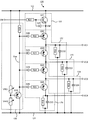
- FIG. 3 shows an example of a detailed configuration of the control unit 100.
- the control unit 100 includes a slow start unit 110, a monitor voltage generation unit 111, a control voltage generation unit 120, a PWM signal generation unit 130, and a constant voltage line LC.
- a voltage Vhigh output from the constant voltage power supply 20 is applied to the constant voltage line LC.
- the monitor voltage generator 111 is connected to the high potential line LH, the low potential line LL, and the constant voltage line LC.
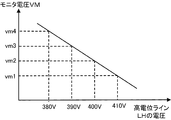
- the monitor voltage generation unit 111 generates a monitor voltage VM and supplies it to the control voltage generation unit 120. As shown in FIG. 4, the monitor voltage VM increases when the voltage of the high potential line LH decreases, and decreases when the voltage of the high potential line LH increases.
- the monitor voltage VM When the voltage of the high potential line LH is the predetermined first voltage (for example, 410 V), the monitor voltage VM is vm1. When the voltage of the high potential line LH is the predetermined second voltage (for example, 400 V), the monitor voltage VM is vm2. When the voltage of the high potential line LH is the predetermined fourth voltage (for example, 390 V), the monitor voltage VM is vm3. When the voltage of the high potential line LH is the predetermined sixth voltage (for example, 380 V), the monitor voltage VM is vm4.
- the slow start unit 110 reduces the monitor voltage VM output by the monitor voltage output unit 111 until a predetermined time elapses after the constant voltage power supply 20 starts to output the voltage Vhigh. As a result, the control voltage generation unit 120 stops operating until a predetermined time elapses, starts operating after the predetermined time elapses, and outputs control voltages VC1 to VC4 described later.
- the control voltage generator 120 is connected to the constant voltage line LC and the high potential line LH.
- the control voltage generator 120 receives the monitor voltage VM.
- the control voltage generator 120 monitors the fluctuation of the DC voltage of the high potential line LH by the monitor voltage VM.
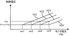
- the control voltage generator 120 generates control voltages VC1 to VC4 based on the monitor voltage VM, and supplies them to the PWM signal generator 130.
- the control voltage generation unit 120 maintains the first control voltage VC1 at a low level voltage (for example, the voltage of the high potential line LH) when the monitor voltage VM is equal to or lower than vm1.
- the control voltage generation unit 120 increases the first control voltage VC1 according to the increase in the monitor voltage VM, and increases the first control voltage VC1 according to the decrease in the monitor voltage VM. Reduce.
- the first control voltage VC1 exceeds the predetermined voltage vcs.
- the control voltage generation unit 120 When the first control voltage VC1 is equal to or lower than the predetermined voltage vcs, the control voltage generation unit 120 maintains the second-stage control voltage VC2 at a low level voltage. Then, when the first control voltage VC1 is equal to or higher than the predetermined voltage vcs, the control voltage generation unit 120 increases the control voltage VC2 at the second stage according to the increase in the monitor voltage VM, and responds according to the decrease in the monitor voltage VM. The control voltage VC2 at the second stage is lowered. When the monitor voltage VM exceeds vm3, the second-stage control voltage VC2 exceeds the predetermined voltage vcs.
- the control voltage generator 120 keeps the third-stage control voltage VC3 at a low level when the second-stage control voltage VC2 is equal to or lower than the predetermined voltage vcs. Then, when the control voltage VC2 at the second stage is equal to or higher than the predetermined voltage vcs, the control voltage generation unit 120 increases the control voltage VC3 at the third stage according to the increase in the monitor voltage VM and decreases the monitor voltage VM. Accordingly, the control voltage VC3 at the third stage is decreased. When the monitor voltage VM exceeds vm4, the third-stage control voltage VC3 exceeds the predetermined voltage vcs.
- the control voltage generator 120 maintains the control voltage VC4 at the fourth stage at a low level.
- the fourth-stage control voltage VC4 is increased according to the increase in the monitor voltage VM, and the fourth-stage control voltage VC4 is decreased according to the decrease in the monitor voltage VM.
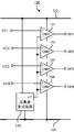
- FIG. 6 shows an example of the configuration of the PWM signal generation unit 130.
- the PWM signal generation unit 130 generates PWM signals VP1 to VP4 having duty ratios corresponding to the control voltages VC1 to VC4 output from the control voltage generation unit 120.
- the PWM signal generation unit 130 includes comparators (comparators) 131 to 134 and a triangular wave generation circuit 135.
- the triangular wave generation circuit 135 is connected to the constant voltage line LC and the high potential line LH.
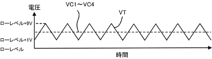
- the triangular wave generation circuit 135 generates a triangular wave voltage VT shown in FIG.
- the minimum voltage of the triangular wave voltage VT is higher than the low level voltage (for example, the voltage of the high potential line LH) in the control voltage VC1 to the control voltage VC4.
- the triangular wave voltage VT is, for example, a triangular wave voltage from a minimum voltage (low level voltage + 1V) to a maximum voltage (low level voltage + 9V).
- the triangular wave voltage VT is supplied to the four comparators 131 to 134 in common.
- the comparator 131 is connected to the constant voltage line LC and the high potential line LH.
- the comparator 131 receives the control voltage VC1 and the triangular wave voltage VT.
- the comparator 131 generates the first PWM signal VP1 based on the control voltage VC1 and the triangular wave voltage VT.
- the PWM signal VP1 becomes a high level voltage (for example, the voltage of the high potential line LH + 20V) when the control voltage VC1 is higher than the triangular wave voltage VT, and a low level voltage (for example, when the control voltage VC1 is lower than the triangular wave voltage VT). , The voltage of the high potential line LH).
- the PWM signal VP1 becomes a pulse wave whose duty ratio increases from 0 to a predetermined value (for example, 100%) as the voltage of the control voltage VC1 increases.
- the comparator 132, the comparator 133, and the comparator 134 generate the second-stage PWM signal VP2, the third-stage PWM signal VP3, and the fourth-stage PWM signal VP4, respectively. These are pulse waves in which the duty ratio gradually increases from 0 to a predetermined value (for example, 100%) as the control voltage VC2, the control voltage VC3, and the control voltage VC4 increase.
- the control voltage generation unit 120, the slow start unit 110, and the monitor voltage generation unit 111 can be realized by a digital circuit or an analog circuit. Further, the functions of the control voltage generation unit 120, the slow start unit 110, and the monitor voltage generation unit 111 can be realized by causing a computer to execute a predetermined program.
- FIG. 8 shows an example of the circuit configuration of the slow start unit 110 and the monitor voltage generation unit 111.
- the slow start unit 110 includes a PNP bipolar transistor Q11, a capacitor C11, a resistor R11, and diodes D11 to D13.
- the resistor R11 has one end connected to the constant voltage line LC and the other end connected to one end of the capacitor C11.
- the other end of the capacitor C11 is connected to the high potential line LH.
- the diode D11 has an anode connected to one end of the capacitor C11 and a cathode connected to the high potential line LH.
- the diode D12 has an anode connected to one end of the capacitor C11 and a cathode connected to the emitter of the transistor Q11.
- the transistor Q11 has a base connected to one end of the capacitor C11 and a collector connected to the other end of the capacitor C11.
- the monitor voltage VM is input to the anode, and the cathode is connected to the emitter of the transistor Q11.
- the monitor voltage generation unit 111 includes an operational amplifier 112, resistors R13 to R17, a variable resistor VR11, a variable resistor VR12, and a diode D14.
- the resistor R13 has one end connected to the constant voltage line LC and the other end connected to one end of the resistor R14.
- the other end of the resistor R14 is connected to the low potential line LL.
- the variable resistor VR11 has one end connected to the constant voltage line LC and the other end connected to one end of the variable resistor VR12.
- the other end of the variable resistor VR12 is connected to the high potential line LH.
- the resistor R15 is connected to the connection point between the other end of the resistor R13 and one end of the resistor R14, and the other end is connected to the non-inverting input (+) of the operational amplifier 112.
- the resistor R16 has one end connected to a connection point between the other end of the variable resistor VR11 and one end of the variable resistor VR12, and the other end connected to the inverting input ( ⁇ ) of the operational amplifier 112.
- the resistor R17 has one end and the other end connected to the output of the operational amplifier 112 and the inverting input ( ⁇ ), respectively.
- the diode D14 has the anode connected to the monitor voltage VM and the cathode connected to the output of the operational amplifier 112.
- the resistor R12 has one end connected to the constant voltage line LC and the other end connected to the anode of the diode D13 and the anode of the diode D14.
- the monitor voltage VM is generated at the connection point between the other end of the resistor R12, the anode of the diode D13, and the anode of the diode D14.
- the slow start unit 110 reduces the monitor voltage VM output by the monitor voltage output unit 111 until a predetermined time elapses after the constant voltage power supply 20 starts to output the voltage Vhigh.
- the potential of the constant voltage line LC is the potential of the high potential line LH.
- the diode D11 discharges the capacitor C11, the charge of the capacitor C11 becomes zero.
- the base voltage of the transistor Q11 is 0 (actually, the potential of the high potential line LH), and the emitter and collector are conducted.
- a current flows through a path indicated by a dashed arrow in FIG. Due to this current, the monitor voltage VM decreases.
- the monitor voltage VM rises and becomes a voltage output by the monitor voltage generation unit 111.
- the monitor voltage generator 111 generates the monitor voltage VM shown in FIG.
- the monitor voltage VM increases when the voltage of the high potential line LH decreases, and decreases when the voltage of the high potential line LH increases.
- the resistance values of the resistors R13 and R14 are, for example, 47 K ⁇ and 1 M ⁇ , respectively.
- the potential difference between the constant voltage line LC and the low potential line LL is divided by the resistors R13 and R14 and input to the non-inverting input (+) of the operational amplifier 112. Further, the potential difference between the constant voltage line LC and the high potential line LH is divided by the variable resistor VR11 and the variable resistor VR12 and input to the inverting input ( ⁇ ) of the operational amplifier 112.
- the operational amplifier 112 amplifies the potential difference between the non-inverting input (+) and the inverting input ( ⁇ ) and outputs the amplified voltage as the monitor voltage VM.
- FIG. 9 shows an example of the circuit configuration of the control voltage generator 120.
- the control voltage generation unit 120 includes a monitor voltage enhancement circuit 121, a first-stage control voltage generation circuit 122, a second-stage control voltage generation circuit 123, a third-stage control voltage generation circuit 124, and a fourth-stage control voltage generation circuit 122.
- Control voltage generation circuit 125 and base voltage adjustment circuit 126 are examples of the control voltage generation circuit 126.
- the monitor voltage enhancement circuit 121 includes an NPN bipolar transistor Q21, a reverse voltage protection diode D21, and a current limiting resistor R21.
- the monitor voltage VM is input to the base of the transistor Q21 through the current limiting resistor R21.
- the collector of the transistor Q21 is connected to the constant voltage line LC.
- the transistor Q21 is an emitter follower.
- the emitter of the transistor Q21 is lower than the monitor voltage VM by the base-emitter voltage Vbe.
- this voltage is referred to as a monitor voltage VM ′ generated at the emitter of the transistor Q21.
- the monitor voltage VM ′ is input to the control signal generation circuit 122 at the first stage.
- a reverse voltage protection diode D21 is connected to the emitter and base of the transistor Q21.
- the first-stage control voltage generation circuit 122 includes a PNP bipolar transistor Q22, a current limiting resistor R22, a reverse current preventing diode D22, a resistor R32, and a capacitor C22.
- the first-stage control voltage generation circuit 122 generates the first control voltage VC1.
- Monitor voltage VM ′ generated at the emitter of transistor Q21 is input to the emitter of transistor Q22.
- the base of the transistor Q22 is connected to one end of the current limiting resistor R22.
- the other end of the current limiting resistor R22 is connected to the anode of the reverse current preventing diode D22.
- An adjustment voltage Vup generated by a base voltage adjustment circuit 126 described later is applied to the cathode of the reverse current prevention diode D22.
- the application of the adjustment voltage Vup to the cathode of the reverse current prevention diode D22 means that the adjustment voltage is input to the base of the transistor Q22.
- the collector of the transistor Q22 is connected to one end of an RC parallel circuit composed of a resistor R32 and a capacitor C22.
- the other end of the RC parallel circuit is connected to the high potential line LH.
- a voltage generated at a connection portion between the collector of the transistor Q22 and one end of the RC parallel circuit is an initial control voltage VC1.
- This RC parallel circuit is provided to remove noise and the like. While the emitter and collector of the transistor Q22 are conducting, the first control voltage VC1 increases as the monitor voltage VM increases, and decreases as the monitor voltage VM decreases. When the emitter and collector of the transistor Q22 are non-conductive, the first control voltage VC1 is a low level voltage (the voltage of the high potential line LH).
- the control voltage generation circuit 123 at the second stage includes a PNP bipolar transistor Q23, a current limiting resistor R23, a reverse current preventing diode D23, a resistor R33, and a capacitor C23.
- the second-stage control voltage generation circuit 123 generates the second-stage control voltage VC2.
- the first control voltage VC1 is input to the emitter of the transistor Q23.
- the transistor Q23, the current limiting resistor R23, the reverse current preventing diode D23, the resistor R33, and the capacitor C23 are the transistor Q22, the current limiting resistor R22, the reverse current preventing diode D22, and the resistor in the first-stage control voltage generation circuit 122.
- R32 and capacitor C22 are connected in the same manner.
- a voltage generated at a connection portion between the collector of the transistor Q23 and one end of the RC parallel circuit is the second-stage control voltage VC2. While the emitter and collector of the transistor Q23 are conducting, the second-stage control voltage VC2 rises as the monitor voltage VM increases, and decreases as the monitor voltage VM decreases. Further, when the emitter and collector of the transistor Q23 are non-conductive, the second-stage control voltage VC2 is a low level voltage.
- the third-stage control voltage generation circuit 124 includes a PNP bipolar transistor Q24, a current limiting resistor R24, a reverse current preventing diode D24, a resistor R34, and a capacitor C24.
- the third-stage control voltage generation circuit 124 generates the third-stage control voltage VC3.
- the second-stage control voltage VC2 is input to the emitter of the transistor Q24.
- the transistor Q24, the current limiting resistor R24, the reverse current preventing diode D24, the resistor R34, and the capacitor C24 are the transistor Q22, the current limiting resistor R22, the reverse current preventing diode D22, and the resistor in the first-stage control voltage generation circuit 22, respectively.
- R32 and capacitor C22 are connected in the same manner.
- a voltage generated at a connection portion between the collector of the transistor Q24 and one end of the RC parallel circuit is the third-stage control voltage VC3. While the emitter and collector of the transistor Q24 are conducting, the control voltage VC3 at the third stage increases as the monitor voltage VM increases, and decreases as the monitor voltage VM decreases. Further, when the emitter and collector of the transistor Q24 are non-conductive, the control voltage VC3 at the third stage is a low level voltage.
- the control voltage generation circuit 125 in the fourth stage includes a PNP bipolar transistor Q25, a current limiting resistor R25, a reverse current preventing diode D25, a resistor R35, and a capacitor C25.
- the fourth-stage control voltage generation circuit 125 generates the fourth-stage control voltage VC4.
- the third-stage control voltage VC3 is input to the emitter of the transistor Q25.
- the transistor Q25, the current limiting resistor R25, the reverse current preventing diode D25, the resistor R35, and the capacitor C25 are the transistor Q22, the current limiting resistor R22, the reverse current preventing diode D22, and the resistor in the control voltage generation circuit 22 in the first stage.
- a voltage generated at a connection portion between the collector of the transistor Q25 and one end of the RC parallel circuit (RC parallel circuit including the resistor R35 and the capacitor C25) is the fourth-stage control voltage VC4. While the emitter and collector of the transistor Q25 are conducting, the fourth-stage control voltage VC4 increases as the monitor voltage VM increases, and decreases as the monitor voltage VM decreases. Further, when the emitter and collector of the transistor Q25 are non-conductive, the fourth-stage control voltage VC4 is a low level voltage.
- the base voltage adjustment circuit 126 includes a resistor R20, a PNP bipolar transistor Q26, a variable resistor VR21, and a variable resistor VR22.
- the resistor R20 has one end connected to the constant voltage line LC and the other end connected to the emitter of the transistor Q26.
- the variable resistor VR21 has one end connected to the constant voltage line LC and the other end connected to one end of the variable resistor VR22.
- the other end of the variable resistor VR22 is connected to the high potential line LH.
- the transistor Q26 has a base connected to a connection portion between the other end of the variable resistor VR21 and one end of the variable resistor VR22, and a collector connected to the high potential line LH.
- the variable resistor VR21 and the variable resistor VR22 divide the potential difference between the voltage of the constant voltage line LC and the voltage of the high potential line LH.
- the transistor Q26 is an emitter follower.
- the emitter of the transistor Q26 has an adjustment voltage Vup that is higher than the voltage divided by the variable resistors VR21 and VR22 by the base-emitter voltage Vbe.
- the base voltage adjustment circuit 126 is connected between the emitters and collectors of the transistors Q22 to Q25 included in the control voltage generation circuits 122 to 125 in accordance with the variation of the monitor voltage VM ′ generated at the emitter of the transistor Q21 included in the monitor voltage enhancement circuit 121.
- the adjustment voltage Vup is generated so that becomes conductive or nonconductive.
- FIG. 10 shows an example of the circuit configuration of the switch SW1 and its periphery in the solar power generation system 1.
- the switch SW1 includes an NMOS transistor 140, a reactor 141, and a diode D31.
- Reactor 141 has one end connected to the cathode of diode D1 and the other end connected to the drain of NMOS transistor 140.
- the diode D31 has an anode and a cathode connected to the other end and one end of the reactor 141, respectively.
- the PWM signal VP1 is input to the gate, and the source is connected to the high potential line LH.
- the NMOS transistor 140 is turned on when the PWM signal VP1 is at a high level voltage (for example, the voltage of the high potential line LH + 20V), and outputs the output voltage of the solar cell string 11 to the high potential line LH.
- the NMOS transistor 140 becomes non-conductive when the PWM signal VP1 is at a low level voltage (for example, the voltage of the high potential line LH), and stops the output of the solar cell string 11 to the high potential line LH.
- Reactor 141 and diode D31 suppress inrush current.
- the cathode of the diode D1 is connected to the low potential line LL via a noise removing capacitor C31.
- the switches SW2 to SW4 have the same configuration as the switch SW1.
- the electric current output from a solar cell string can be adjusted according to the power consumption of a load apparatus etc. or the intensity of sunlight.
- each switch can be reduced in size.
- the next switch can start switching after the previous switch is always turned on, and in this case, switching noise can be greatly reduced. it can.
- FIG. 11 shows an example of the configuration of the photovoltaic power generation system 2 according to the second embodiment of the present invention.
- the solar power generation system 2 includes solar cell strings 15 to 18, switches SW1 to SW4, a constant voltage power supply 20, a control unit 100, a high potential line LH, a low potential line LL, diodes D9 and D41 to D43. , D45 to D48, and a capacitor C1.
- the switches SW1 to SW4, the constant voltage power supply 20, the control unit 100, the high potential line LH, the low potential line LL, the capacitor C1, and the diode D9 of the photovoltaic power generation system 2 according to the second embodiment are as follows.
- the configuration is the same as that of the photovoltaic power generation system 1 according to the first embodiment.
- the solar cell strings 15 to 18 are connected in series. That is, in the first solar cell string 15, the output Vout is connected to the high potential line LH and the ground GD is connected to the low potential line LL via the switch SW1 whose opening / closing is controlled by the first PWM signal VP1. Then, except for the last solar cell string 18, the output Vout of the preceding solar cell string is connected to the ground GD of the subsequent solar cell string.
- the output Vout is added to the switches SW 1, SW 2, and SW 3 and the backflow prevention diode D 41 connected in series with them. , D42, D43 to be connected to the high potential line LH.
- the last-stage solar cell string 18 is connected to the high potential line LH via the switch SW4.
- the final-stage solar cell string 18 is also connected to the switch SW4 and connected to the high-voltage line LH via a backflow prevention diode connected in series therewith. It may be connected to the potential line LH.
- the diode D45 has an anode connected to the ground GD of the solar cell string 15 and a cathode connected to the output Vout of the solar cell string 15. That is, the diode D45 is connected to the solar cell string 15 in a direction in which a current flows from the ground GD to the output Vout. Similarly, diodes D46 to D48 are connected to the solar cell strings 16 to 18 in a direction in which current flows from the ground GD to the output Vout. Moreover, unlike the photovoltaic power generation system 1 according to the first embodiment, in the photovoltaic power generation system 2 according to the second embodiment, the voltage input Vin of the constant voltage power supply 20 is output to the output of the solar cell string 18 at the final stage. Vout is connected.
- FIG. 12 shows an example of a current flow when the intensity of sunlight varies in the photovoltaic power generation system 2.
- the intensity of sunlight varies depending on the season such as summer and winter and the time zone such as morning and evening and noon.
- the stronger the sunlight the higher the output voltage of the individual solar cell strings.
- FIG. 12A when each of the solar cell strings 15 to 18 outputs a voltage of 230 V when the voltage of the high potential line LH is 400 V, the solar cell string 16 and the solar cell string 17 And the output voltage of the solar cell string 18 are 460V, 690V, and 920V, respectively.
- the switch SW1 is always closed, and the switches SW3 and SW4 are always open.
- the switch SW2 is subjected to PWM control so that the high potential line LH becomes 400V, and is repeatedly opened and closed.
- the current flows through the solar cell string 15, the solar cell string 16, and the switch SW2. Even if the switch SW1 is closed, no current flows through the switch SW1 because it is blocked by the backflow prevention diode D41.
- FIG. 12B when each of the solar cell strings 15 to 18 outputs a voltage of 100 V when the voltage of the high potential line LH is 400 V, the solar cell string 16 and the solar cell The output voltages of the string 17 and the solar cell string 18 are 200V, 300V, and 400V, respectively.
- all the switches SW1 to SW4 are always closed. Current flows through each solar cell string 15-18 and the switch SW4. No current flows through each of the switches SW1 to SW3 by being blocked by the backflow prevention diodes D41 to D43.
- FIG. 13 shows an example of a current flow when the solar cell string 15 and the solar cell string 16 are shaded in the solar power generation system 2.
- the output voltage of these solar cell strings decreases.
- the voltage of the high potential line LH is 400V
- the output voltage of the solar cell string 15 and the solar cell string 16 is approximately 0V
- the solar cell string 17 and the solar cell string 18 each output a voltage of 230V.
- the switches SW1 to SW3 are always closed, and the switch SW4 is subjected to PWM control so that the high potential line LH becomes 400V, and is repeatedly opened and closed.
- the current flows through the diode D45, the diode D46, the solar cell string 17, the solar cell string 18, and the switch SW4. Since no current flows through the solar cell string 15 and the solar cell string 16, no voltage drop occurs.
- the solar cell system concerning this invention is not restricted to four pieces, Two solar cell strings and three pieces Or 5 or more.
- a control part outputs a PWM signal according to the number of solar cell strings.
- FIG. 10 described above an example in which an NMOS transistor is used as a switching element is shown, but a relay can also be used as a switching element.
Landscapes
- Engineering & Computer Science (AREA)
- Power Engineering (AREA)
- Dc-Dc Converters (AREA)
Abstract
複数の太陽電池ストリングの出力を負荷装置等の消費電力や日差しの強さに応じて調節する。 低電位ラインLLの電圧は基準電位である。高電位ラインLHの電圧は基準電位に対して高電位の直流電圧である。太陽電池ストリング11~14は、高電位ラインLHに電圧を出力する。制御部100は、高電位ラインLHの電圧が例えば410V以下であるときにPWM信号VP1を出力する。PWM信号VP1は、高電位ラインLHにおける電圧の低下に応じて増加し、その電圧の上昇に応じて減少するデューティ比を有するパルス波である。各PWM信号VP2~VP4もPWM信号VP1と同様のパルス波である。制御部100は、PWM信号VP1に続いて、順次前段のPWM信号が所定のデューティ比以上であるときに各PWM信号VP2~VP4を出力する。スイッチSW1~SW4は、各PWM信号VP1~VP4によって個々に開閉が制御される。
Description
本発明は、複数の太陽電池ストリングを含む太陽光発電システムに関する。
太陽光発電システムは、通常複数の太陽電池ストリングを含む。一般に、太陽電池ストリングは直列接続された複数の太陽電池モジュールを含んでいる。
直流給電システムでは、複数の太陽電池ストリングは逆流防止ダイオードを介して直流バスに並列に接続される。逆流防止ダイオードは、直流バスから各太陽電池ストリングに電流が逆流することを防ぐ。
また、交流給電システムでも、同様に、複数の太陽電池ストリングは逆流防止ダイオードを介して並列に接続される。そして、逆流防止ダイオードを通過した直流電力はインバータによって交流電力に変換され、交流電力が交流バスに供給される。
直流給電システムでは、複数の太陽電池ストリングは逆流防止ダイオードを介して直流バスに並列に接続される。逆流防止ダイオードは、直流バスから各太陽電池ストリングに電流が逆流することを防ぐ。
また、交流給電システムでも、同様に、複数の太陽電池ストリングは逆流防止ダイオードを介して並列に接続される。そして、逆流防止ダイオードを通過した直流電力はインバータによって交流電力に変換され、交流電力が交流バスに供給される。
直流バスや交流バスに接続されている負荷装置の消費電力は、一般に時々刻々と変動する。負荷装置で消費される電力が減少し、太陽光発電システムによって出力される電力が負荷装置で消費される電力を超えた場合、直流バスや交流バスの電圧が上昇し、負荷装置が異常動作したり、破壊されたりするおそれがある。
また、季節や時間帯によって日差しの強さは変わる。日差しの強さが変動すると、太陽電池の出力は変動する。
また、季節や時間帯によって日差しの強さは変わる。日差しの強さが変動すると、太陽電池の出力は変動する。
本発明の目的は、複数の太陽電池ストリングの出力を負荷装置等の消費電力や日差しの強さに応じて調節することができる太陽光発電システムを提供することである。
上記目的を達成するために、本発明の太陽光発電システムは、
電圧が、基準電位である第1の電源ラインと
電圧が、前記基準電位に対して高電位の直流電圧である第2の電源ラインと、
前記第2の電源ラインに電圧を出力する複数の太陽電池ストリングと、
前記第2の電源ラインの電圧が所定の電圧以下であるときに前記第2の電源ラインにおける電圧の低下に応じて増加し、当該電圧の上昇に応じて減少するデューティ比を有するパルス波である最初のPWM信号を出力し、順次前段のPWM信号が所定のデューティ比以上であるときに前記第2の電源ラインにおける電圧の低下に応じて増加し、当該電圧の上昇に応じて減少するデューティ比を有するパルス波である各PWM信号を出力する制御部と、
前記各太陽電池ストリングの出力と前記第2の電源ラインとの間にそれぞれ設置されており、前記制御部によって生成された各PWM信号によって個々に開閉が制御される複数のスイッチと、
を備えることを特徴とする。
電圧が、基準電位である第1の電源ラインと
電圧が、前記基準電位に対して高電位の直流電圧である第2の電源ラインと、
前記第2の電源ラインに電圧を出力する複数の太陽電池ストリングと、
前記第2の電源ラインの電圧が所定の電圧以下であるときに前記第2の電源ラインにおける電圧の低下に応じて増加し、当該電圧の上昇に応じて減少するデューティ比を有するパルス波である最初のPWM信号を出力し、順次前段のPWM信号が所定のデューティ比以上であるときに前記第2の電源ラインにおける電圧の低下に応じて増加し、当該電圧の上昇に応じて減少するデューティ比を有するパルス波である各PWM信号を出力する制御部と、
前記各太陽電池ストリングの出力と前記第2の電源ラインとの間にそれぞれ設置されており、前記制御部によって生成された各PWM信号によって個々に開閉が制御される複数のスイッチと、
を備えることを特徴とする。
好ましくは、本発明の太陽光発電システムは、
前記制御部が、
前記第2の電源ラインの電圧が低下すると上昇し、前記第2の電源ラインの電圧が上昇すると低下するモニタ電圧を生成するモニタ電圧生成部と、
前記モニタ電圧生成部によって生成されるモニタ電圧が所定の電圧以上であるときに前記モニタ電圧の上昇に応じて最初の制御電圧を上昇させ、前記モニタ電圧の低下に応じて当該最初の制御電圧を低下させ、順次前段の制御電圧が所定の電圧以上であるときに前記モニタ電圧の上昇に応じて各制御電圧を上昇させ、前記モニタ電圧の低下に応じて当該各制御電圧を低下させる制御電圧生成部と、
前記制御電圧生成部から出力される各制御電圧に応じたデューティ比を有する前記各PWM信号を生成するPWM信号生成部と、
を含む、
ことを特徴とする。
前記制御部が、
前記第2の電源ラインの電圧が低下すると上昇し、前記第2の電源ラインの電圧が上昇すると低下するモニタ電圧を生成するモニタ電圧生成部と、
前記モニタ電圧生成部によって生成されるモニタ電圧が所定の電圧以上であるときに前記モニタ電圧の上昇に応じて最初の制御電圧を上昇させ、前記モニタ電圧の低下に応じて当該最初の制御電圧を低下させ、順次前段の制御電圧が所定の電圧以上であるときに前記モニタ電圧の上昇に応じて各制御電圧を上昇させ、前記モニタ電圧の低下に応じて当該各制御電圧を低下させる制御電圧生成部と、
前記制御電圧生成部から出力される各制御電圧に応じたデューティ比を有する前記各PWM信号を生成するPWM信号生成部と、
を含む、
ことを特徴とする。
好ましくは、本発明の太陽光発電システムは、
1つ以上の前記太陽電池ストリングが出力する電圧を、前記第2の電源ラインの電圧より高く、かつ前記第2の電源ラインの電圧との差が一定である電圧に変換する絶縁型のDC/DCコンバータを含み、当該変換された電圧を出力する定電圧電源を備え、
前記制御部が、前記定電圧電源が出力する電圧と前記第2の電源ラインの電圧との差である電圧によって動作する、
ことを特徴とする。
1つ以上の前記太陽電池ストリングが出力する電圧を、前記第2の電源ラインの電圧より高く、かつ前記第2の電源ラインの電圧との差が一定である電圧に変換する絶縁型のDC/DCコンバータを含み、当該変換された電圧を出力する定電圧電源を備え、
前記制御部が、前記定電圧電源が出力する電圧と前記第2の電源ラインの電圧との差である電圧によって動作する、
ことを特徴とする。
好ましくは、本発明の太陽光発電システムは、
前記制御部が、前記定電圧電源が電圧を出力し始めてから所定の時間が経過するまで前記モニタ電圧出力部によって出力されるモニタ電圧を低下させるスロースタート部を含むことを特徴とする。
前記制御部が、前記定電圧電源が電圧を出力し始めてから所定の時間が経過するまで前記モニタ電圧出力部によって出力されるモニタ電圧を低下させるスロースタート部を含むことを特徴とする。
好ましくは、本発明の太陽光発電システムは、
前記制御電圧生成部が、
エミッタフォロワであるNPNバイポーラトランジスタを含み、当該NPNバイポーラトランジスタのベースに前記モニタ電圧生成部によって生成されたモニタ電圧が入力され、エミッタにモニタ電圧が生じるモニタ電圧強化回路と、
ベースに調整電圧が入力され、コレクタに前記各制御電圧が生じるPNPバイポーラトランジスタを含む複数段の制御電圧生成回路であって、1段目の当該制御電圧生成回路に含まれるPNPバイポーラトランジスタのエミッタには前記モニタ電圧強化回路に含まれるNPNバイポーラトランジスタのエミッタに生じるモニタ電圧が入力され、2段目以降の当該制御電圧生成回路に含まれるPNPバイポーラトランジスタのエミッタには前段の制御電圧生成回路に含まれるPNPバイポーラトランジスタのコレクタに生じる制御電圧が入力される制御電圧生成回路と、
前記モニタ電圧強化回路に含まれるNPNバイポーラトランジスタのエミッタに生じるモニタ電圧の変動に応じて前記各制御電圧生成回路に含まれるPNPバイポーラトランジスタのエミッタ・コレクタ間が導通または非導通となるように、前記調整電圧を生成するベース電圧調整回路と、
を備える、
ことを特徴とする。
前記制御電圧生成部が、
エミッタフォロワであるNPNバイポーラトランジスタを含み、当該NPNバイポーラトランジスタのベースに前記モニタ電圧生成部によって生成されたモニタ電圧が入力され、エミッタにモニタ電圧が生じるモニタ電圧強化回路と、
ベースに調整電圧が入力され、コレクタに前記各制御電圧が生じるPNPバイポーラトランジスタを含む複数段の制御電圧生成回路であって、1段目の当該制御電圧生成回路に含まれるPNPバイポーラトランジスタのエミッタには前記モニタ電圧強化回路に含まれるNPNバイポーラトランジスタのエミッタに生じるモニタ電圧が入力され、2段目以降の当該制御電圧生成回路に含まれるPNPバイポーラトランジスタのエミッタには前段の制御電圧生成回路に含まれるPNPバイポーラトランジスタのコレクタに生じる制御電圧が入力される制御電圧生成回路と、
前記モニタ電圧強化回路に含まれるNPNバイポーラトランジスタのエミッタに生じるモニタ電圧の変動に応じて前記各制御電圧生成回路に含まれるPNPバイポーラトランジスタのエミッタ・コレクタ間が導通または非導通となるように、前記調整電圧を生成するベース電圧調整回路と、
を備える、
ことを特徴とする。
好ましくは、本発明の太陽光発電システムは、
前記PWM信号生成部が、
三角波電圧を出力する三角波生成回路と、
前記制御電圧生成部から出力される前記各制御電圧を個々に前記三角波電圧と比較し、前記各制御電圧が前記三角波電圧より高いときに前記各スイッチが閉じるレベルとなり、前記各制御電圧が前記三角波電圧より低いときに前記各スイッチが開くレベルとなる前記PWM信号を出力する複数のコンパレータと、
を備える、
ことを特徴とする。
前記PWM信号生成部が、
三角波電圧を出力する三角波生成回路と、
前記制御電圧生成部から出力される前記各制御電圧を個々に前記三角波電圧と比較し、前記各制御電圧が前記三角波電圧より高いときに前記各スイッチが閉じるレベルとなり、前記各制御電圧が前記三角波電圧より低いときに前記各スイッチが開くレベルとなる前記PWM信号を出力する複数のコンパレータと、
を備える、
ことを特徴とする。
好ましくは、本発明の太陽光発電システムは、
前記各スイッチが、NMOSトランジスタを含み、前記各PWM信号が当該NMOSトランジスタのゲートに入力されることを特徴とする。
前記各スイッチが、NMOSトランジスタを含み、前記各PWM信号が当該NMOSトランジスタのゲートに入力されることを特徴とする。
好ましくは、本発明の太陽光発電システムは、
前記各太陽電池ストリングにおいて、グランドが前記第1の電源ラインに接続され、出力が前記スイッチを介して前記第2の電源ラインに接続されている、
ことを特徴とする。
前記各太陽電池ストリングにおいて、グランドが前記第1の電源ラインに接続され、出力が前記スイッチを介して前記第2の電源ラインに接続されている、
ことを特徴とする。
好ましくは、本発明の太陽光発電システムは、
前記最初のPWM信号によって開閉が制御されるスイッチを介して出力が前記第2の電源ラインに接続された最初の太陽電池ストリングにおいて、グランドが前記第1の電源ラインに接続され、
前記最初の太陽電池ストリングを除き、前段の太陽電池ストリングの出力が次段の太陽電池ストリングのグランドに接続され、
出力電圧が最も高い最終段の太陽電池ストリングを除く各太陽電池ストリングにおいて、直列に接続された逆流防止ダイオードと前記スイッチとを介して出力が前記第2の電源ラインに接続される、
ことを特徴とする。
前記最初のPWM信号によって開閉が制御されるスイッチを介して出力が前記第2の電源ラインに接続された最初の太陽電池ストリングにおいて、グランドが前記第1の電源ラインに接続され、
前記最初の太陽電池ストリングを除き、前段の太陽電池ストリングの出力が次段の太陽電池ストリングのグランドに接続され、
出力電圧が最も高い最終段の太陽電池ストリングを除く各太陽電池ストリングにおいて、直列に接続された逆流防止ダイオードと前記スイッチとを介して出力が前記第2の電源ラインに接続される、
ことを特徴とする。
好ましくは、本発明の太陽光発電システムは、
前記各太陽電池ストリングにおいて、グランドから出力に電流が流れる向きにダイオードが接続されていることを特徴とする。
前記各太陽電池ストリングにおいて、グランドから出力に電流が流れる向きにダイオードが接続されていることを特徴とする。
本発明によれば、複数の太陽電池ストリングの出力を負荷装置等の消費電力や日差しの強さに応じて調節することができる。
以下、本発明の実施形態に係る太陽光発電システムについて図面を参照しながら詳細に説明する。なお、実施形態を説明する全図において、共通の構成要素には同一の符号を付し、繰り返しの説明を省略する。
図1は、本発明の第1の実施形態に係る太陽光発電システム1の構成の一例を示す。
太陽光発電システム1は、太陽電池ストリング11~14と、スイッチSW1~SW4と、定電圧電源20と、制御部100と、高電位ラインLHと、低電位ラインLLと、ダイオードD1~D9と、コンデンサC1とを有する。
スイッチSW1~SW4は、それぞれ太陽電池ストリング11~14の出力Voutと高電位ラインLHとの間に設置される。太陽電池ストリング11の出力Voutは、ダイオードD1のアノードに接続される。ダイオードD1のカソードは、スイッチSW1の一端に接続される。スイッチSW1の他端は、高電位ラインLHに接続される。太陽電池ストリング11のグランドGDは、低電位ラインLLに接続される。同様に、太陽電池ストリング12~14の出力Voutは、それぞれダイオードD2~D4のアノードに接続される。ダイオードD2~D4のカソードは、それぞれスイッチSW2~SW4の一端に接続される。スイッチSW2~W4の他端は、それぞれ高電位ラインLHに接続される。太陽電池ストリング12~14のグランドGDは、それぞれ低電位ラインLLに接続される。
なお、太陽電池ストリング11~14の出力VoutがそれぞれスイッチSW1~SW4の一端に接続され、スイッチSW1~SW4の他端がそれぞれダイオードD1~D4のアノードに接続され、ダイオードD1~D4のカソードがそれぞれ高電位ラインLHに接続されていてもよい。
太陽光発電システム1は、太陽電池ストリング11~14と、スイッチSW1~SW4と、定電圧電源20と、制御部100と、高電位ラインLHと、低電位ラインLLと、ダイオードD1~D9と、コンデンサC1とを有する。
スイッチSW1~SW4は、それぞれ太陽電池ストリング11~14の出力Voutと高電位ラインLHとの間に設置される。太陽電池ストリング11の出力Voutは、ダイオードD1のアノードに接続される。ダイオードD1のカソードは、スイッチSW1の一端に接続される。スイッチSW1の他端は、高電位ラインLHに接続される。太陽電池ストリング11のグランドGDは、低電位ラインLLに接続される。同様に、太陽電池ストリング12~14の出力Voutは、それぞれダイオードD2~D4のアノードに接続される。ダイオードD2~D4のカソードは、それぞれスイッチSW2~SW4の一端に接続される。スイッチSW2~W4の他端は、それぞれ高電位ラインLHに接続される。太陽電池ストリング12~14のグランドGDは、それぞれ低電位ラインLLに接続される。
なお、太陽電池ストリング11~14の出力VoutがそれぞれスイッチSW1~SW4の一端に接続され、スイッチSW1~SW4の他端がそれぞれダイオードD1~D4のアノードに接続され、ダイオードD1~D4のカソードがそれぞれ高電位ラインLHに接続されていてもよい。
また、太陽電池ストリング11の出力Voutは、ダイオードD5のアノードに接続される。同様に、太陽電池ストリング12~14の出力Voutは、それぞれダイオードD6~D8のアノードに接続される。ダイオードD6~D8のカソードは1つにまとめられて全て定電圧電源20の電圧入力Vinに接続される。なお、太陽電池ストリング11~14の出力Voutはいずれか1つ以上がダイオードD5~D8を介して定電圧電源20の電圧入力Vinに接続されていればよい。定電圧電源20のシグナルグランドSGとグランドGDは、それぞれ高電位ラインLHと低電位ラインLLに接続される。定電圧電源20の電圧出力Vhighは、制御部100の電圧入力Vhighに接続される。
制御部100のシグナルグランドSGとグランドGDは、それぞれ高電位ラインLHと低電位ラインLLに接続される。制御部100のPWM(Pulse Width Modulation)信号VP1は、スイッチSW1の開閉を制御する。同様に、制御部100のPWM信号VP2~VP4は、それぞれスイッチSW2~SW4の開閉を制御する。
コンデンサC1は、一端が高電位ラインLHに接続され、他端が低電位ラインLLに接続される。コンデンサC1は、高電位ラインLHの電圧におけるノイズを除去する。高電位ラインLHはダイオードD9のアノードに接続される。ダイオードD9のカソードは、端子T1に接続される。ダイオードD9は、逆流防止ダイオードである。低電位ラインLLは端子T2に接続される。
制御部100のシグナルグランドSGとグランドGDは、それぞれ高電位ラインLHと低電位ラインLLに接続される。制御部100のPWM(Pulse Width Modulation)信号VP1は、スイッチSW1の開閉を制御する。同様に、制御部100のPWM信号VP2~VP4は、それぞれスイッチSW2~SW4の開閉を制御する。
コンデンサC1は、一端が高電位ラインLHに接続され、他端が低電位ラインLLに接続される。コンデンサC1は、高電位ラインLHの電圧におけるノイズを除去する。高電位ラインLHはダイオードD9のアノードに接続される。ダイオードD9のカソードは、端子T1に接続される。ダイオードD9は、逆流防止ダイオードである。低電位ラインLLは端子T2に接続される。
太陽光発電システム1が直流給電システムに接続される場合には、端子T1と端子T2は直流バスに接続され、直流バスに負荷装置等が接続される。
太陽光発電システム1が交流給電システムに接続される場合には、端子T1と端子T2はインバータの入力に接続され、インバータの出力が交流バスに接続される。交流バスには負荷装置等が接続される。
太陽光発電システム1が交流給電システムに接続される場合には、端子T1と端子T2はインバータの入力に接続され、インバータの出力が交流バスに接続される。交流バスには負荷装置等が接続される。
低電位ラインLLの電圧は、基準電位である。高電位ラインLHの電圧は、基準電位に対して高電位の直流電圧である。低電位ラインLLと高電位ラインLHの電圧は、例えば、それぞれ0V(接地電位)と400Vである。または、低電位ラインLLと高電位ラインLHの電圧は、例えば、それぞれ-200Vと+200Vであってもよい。ただし、高電位ラインLHの電圧は、太陽電池ストリング11~14の出力電圧Voutの変動や負荷装置の消費電力の変動等により変動する。例えば、負荷装置の消費電力が増加すると、高電位ラインLHの電圧は低下する。
太陽電池ストリング11~14は、それぞれ直列接続された複数の太陽電池モジュールを含んでいる。太陽電池ストリング11~14は、それぞれスイッチSW1~SW4が閉じているときに高電位ラインLHに電圧を出力する。
なお、低電位ラインLLは本発明の第1の電源ラインの例であり、高電位ラインLHは本発明の第2の電源ラインの例である。
太陽電池ストリング11~14は、それぞれ直列接続された複数の太陽電池モジュールを含んでいる。太陽電池ストリング11~14は、それぞれスイッチSW1~SW4が閉じているときに高電位ラインLHに電圧を出力する。
なお、低電位ラインLLは本発明の第1の電源ラインの例であり、高電位ラインLHは本発明の第2の電源ラインの例である。
定電圧電源20は、絶縁型のDC/DC(直流/直流)コンバータを含む。DC/DCコンバータは、太陽電池ストリング11~14が出力する電圧を、高電位ラインLHの電圧より高く、かつ高電位ラインLHの電圧との差(例えば、24V)が一定である電圧に変換する。定電圧電源20は、変換された電圧Vhighを出力する。例えば、高電位ラインLHの電圧が400Vであるとき、定電圧電源20の出力電圧Vhighは424Vである。
制御部100は、定電圧電源20が出力する電圧Vhighと高電位ラインLHの電圧との差である電圧(例えば、24V)によって動作する。
制御部100は、PWM信号VP1~VP4を出力する。PWM信号VP1~VP4はパルス波である。PWM信号VP1~VP4のローレベルの電圧は高電位ラインLHの電圧である。
制御部100は、PWM信号VP1~VP4を出力する。PWM信号VP1~VP4はパルス波である。PWM信号VP1~VP4のローレベルの電圧は高電位ラインLHの電圧である。
図2は、高電位ラインLHの電圧とPWM信号の関係の一例を示す。
制御部100は、高電位ラインLHの電圧が所定の第1の電圧(例えば、410V)以下であるとき、最初のPWM信号VP1のデューティ比を高電位ラインLHにおける電圧の低下に応じて増加させ、その電圧の上昇に応じて減少させる。図2に示すように、高電位ラインLHの電圧が所定の第2の電圧(例えば、400V)であるとき、最初のPWM信号VP1のデューティ比は90%であり、PWM信号VP2~VP4のデューティ比は0である。高電位ラインLHの電圧が所定の第3の電圧(例えば、398V)であるとき、最初のPWM信号VP1のデューティ比は100%である。
制御部100は、高電位ラインLHの電圧が所定の第1の電圧(例えば、410V)以下であるとき、最初のPWM信号VP1のデューティ比を高電位ラインLHにおける電圧の低下に応じて増加させ、その電圧の上昇に応じて減少させる。図2に示すように、高電位ラインLHの電圧が所定の第2の電圧(例えば、400V)であるとき、最初のPWM信号VP1のデューティ比は90%であり、PWM信号VP2~VP4のデューティ比は0である。高電位ラインLHの電圧が所定の第3の電圧(例えば、398V)であるとき、最初のPWM信号VP1のデューティ比は100%である。
制御部100は、高電位ラインLHの電圧が上記所定の第2の電圧(例えば、400V)以下である(すなわち、最初のPWM信号VP1のデューティ比が所定のデューティ比、例えば90%以上である)とき、2段目のPWM信号VP2のデューティ比を高電位ラインLHにおける電圧の低下に応じて増加させ、その電圧の上昇に応じて減少させる。図2に示すように、高電位ラインLHの電圧が所定の第4の電圧(例えば、390V)であるとき、2段目のPWM信号VP2のデューティ比は90%である。このとき、最初のPWM信号VP1のデューティ比は100%であり、3段目のPWM信号VP3と4段目のPWM信号VP4のデューティ比は0である。高電位ラインLHの電圧が所定の第5の電圧(例えば、388V)であるとき、2段目のPWM信号VP2のデューティ比は100%である。
制御部100は、高電位ラインLHの電圧が上記所定の第4の電圧(例えば、390V)以下である(すなわち、2段目のPWM信号VP2のデューティ比が所定のデューティ比、例えば90%以上である)とき、3段目のPWM信号VP3のデューティ比を高電位ラインLHにおける電圧の低下に応じて増加させ、その電圧の上昇に応じて減少させる。図2に示すように、高電位ラインLHの電圧が所定の第6の電圧(例えば、380V)であるとき、3段目のPWM信号VP3のデューティ比は90%である。このとき、最初のPWM信号VP1と2段目のPWM信号VP2のデューティ比は100%であり、4段目のPWM信号VP4のデューティ比は0である。高電位ラインLHの電圧が所定の第7の電圧(例えば、378V)であるとき、3段目のPWM信号VP3のデューティ比は100%である。
制御部100は、高電位ラインLHの電圧が上記所定の第6の電圧(例えば、380V)以下である(すなわち、3段目のPWM信号VP3のデューティ比が所定のデューティ比、例えば90%以上である)とき、4段目のPWM信号VP4のデューティ比を電位ラインLHにおける電圧の低下に応じて増加させ、その電圧の上昇に応じて減少させる。図2に示すように、高電位ラインLHの電圧が所定の第8の電圧(例えば、370V)であるとき、4段目のPWM信号VP4のデューティ比は90%である。このとき、PWM信号VP1~VP3のデューティ比は100%である。高電位ラインLHの電圧が所定の第9の電圧(例えば、368V)であるとき、4段目のPWM信号VP4のデューティ比は100%である。
例えば、PWM信号VP1がハイレベルの電圧であるときにスイッチSW1は閉じ、PWM信号VP1がローレベルの電圧であるときにスイッチSW1は開く。太陽電池ストリング11は、スイッチSW1が閉じているときに高電位ラインLHに電圧を出力し、スイッチSW1が開いているときには高電位ラインLHへの電圧の出力を停止する。スイッチSW2~スイッチSW4もPWM信号VP2~VP4によってスイッチSW1と同様に動作する。
このため、PWM信号VP1~VP4のデューティ比が増加するとき高電位ラインLHの電圧は上昇し、それらのデューティ比が減少するとき高電位ラインLHの電圧は減少する。
このため、PWM信号VP1~VP4のデューティ比が増加するとき高電位ラインLHの電圧は上昇し、それらのデューティ比が減少するとき高電位ラインLHの電圧は減少する。
例えば、負荷装置の電力消費が増加すると、高電位ラインLHの電圧は低下する。図2に示すように、高電位ラインLHの電圧が上記所定の第1の電圧(例えば、410V)と上記所定の第2の電圧(例えば、400V)との間にあるときに、高電位ラインLHの電圧が減少した場合、制御部100はPWM信号VP1のデューティ比を増加させて高電位ラインLHの電圧を上昇させる。
そして、高電位ラインLHの電圧が上記所定の第2の電圧(例えば、400V)より低くなる(すなわち、PWM信号VP1のデューティ比が90%以上になる)と、制御部100は2段目のPWM信号VP2のデューティ比も増加させて高電位ラインLHの電圧を上昇させる。
そして、高電位ラインLHの電圧が上記所定の第2の電圧(例えば、400V)より低くなる(すなわち、PWM信号VP1のデューティ比が90%以上になる)と、制御部100は2段目のPWM信号VP2のデューティ比も増加させて高電位ラインLHの電圧を上昇させる。
同様に、高電位ラインLHの電圧が上記所定の第4の電圧(例えば、390V)より低くなる(すなわち、PWM信号VP2のデューティ比が90%以上になる)と、制御部100は3段目のPWM信号VP3のデューティ比を増加させて高電位ラインLHの電圧を上昇させる。
高電位ラインLHの電圧が上記所定の第6の電圧(例えば、380V)より低くなる(すなわち、PWM信号VP3のデューティ比が90%以上になる)と、制御部100は4段目のPWM信号VP4のデューティ比を増加させて高電位ラインLHの電圧を上昇させる。
高電位ラインLHの電圧が上記所定の第6の電圧(例えば、380V)より低くなる(すなわち、PWM信号VP3のデューティ比が90%以上になる)と、制御部100は4段目のPWM信号VP4のデューティ比を増加させて高電位ラインLHの電圧を上昇させる。
なお、上記では、制御部100は、PWM信号VP1~VP3のデューティ比が90%以上であるとき、次段のPWM信号VP2~VP4のデューティ比を高電位ラインLHにおける電圧の低下に応じて増加させ、その電圧の上昇に応じて減少させるとしたが、制御部100は、PWM信号VP1~VP3が予め設定された任意のデューティ比以上であるとき、次段のPWM信号VP2~VP4のデューティ比を高電位ラインLHにおける電圧の低下に応じて増加させ、その電圧の上昇に応じて減少させることができる。例えば、制御部100は、PWM信号VP1~VP3のデューティ比が100%であるとき、次段のPWM信号VP2~VP4のデューティ比を高電位ラインLHにおける電圧の低下に応じて増加させ、その電圧の上昇に応じて減少させることができる。
制御部100は、デジタル回路でもアナログ回路でも実現することができる。また、CPU(Central Processing Unit)と、RAM(Random Access Memory)等で構成される主メモリと、フラッシュメモリやハードディスク等で構成される記憶部とを備えたコンピュータに所定のプログラムを実行させることにより制御部100の機能を実現することもできる。
図3は、制御部100の詳細な構成の一例を示す。
制御部100は、スロースタート部110と、モニタ電圧生成部111と、制御電圧生成部120と、PWM信号生成部130と、定電圧ラインLCとを有する。
定電圧ラインLCには、定電圧電源20によって出力される電圧Vhighが印加される。
モニタ電圧生成部111は、高電位ラインLHと低電位ラインLLと定電圧ラインLCとに接続される。モニタ電圧生成部111は、モニタ電圧VMを生成し、制御電圧生成部120に供給する。図4に示すように、モニタ電圧VMは、高電位ラインLHの電圧が低下すると上昇し、高電位ラインLHの電圧が上昇すると低下する。高電位ラインLHの電圧が上記所定の第1の電圧(たとえば、410V)であるとき、モニタ電圧VMはvm1である。また、高電位ラインLHの電圧が上記所定の第2の電圧(たとえば、400V)であるとき、モニタ電圧VMはvm2である。高電位ラインLHの電圧が上記所定の第4の電圧(たとえば、390V)であるとき、モニタ電圧VMはvm3である。高電位ラインLHの電圧が上記所定の第6の電圧(たとえば、380V)であるとき、モニタ電圧VMはvm4である。
スロースタート部110は、定電圧電源20が電圧Vhighを出力し始めてから所定の時間が経過するまでモニタ電圧出力部111によって出力されるモニタ電圧VMを低下させる。これにより、制御電圧生成部120は、所定の時間が経過するまで動作を停止しており、所定の時間が経過してから動作を開始し、後述する制御電圧VC1~VC4を出力する。
制御部100は、スロースタート部110と、モニタ電圧生成部111と、制御電圧生成部120と、PWM信号生成部130と、定電圧ラインLCとを有する。
定電圧ラインLCには、定電圧電源20によって出力される電圧Vhighが印加される。
モニタ電圧生成部111は、高電位ラインLHと低電位ラインLLと定電圧ラインLCとに接続される。モニタ電圧生成部111は、モニタ電圧VMを生成し、制御電圧生成部120に供給する。図4に示すように、モニタ電圧VMは、高電位ラインLHの電圧が低下すると上昇し、高電位ラインLHの電圧が上昇すると低下する。高電位ラインLHの電圧が上記所定の第1の電圧(たとえば、410V)であるとき、モニタ電圧VMはvm1である。また、高電位ラインLHの電圧が上記所定の第2の電圧(たとえば、400V)であるとき、モニタ電圧VMはvm2である。高電位ラインLHの電圧が上記所定の第4の電圧(たとえば、390V)であるとき、モニタ電圧VMはvm3である。高電位ラインLHの電圧が上記所定の第6の電圧(たとえば、380V)であるとき、モニタ電圧VMはvm4である。
スロースタート部110は、定電圧電源20が電圧Vhighを出力し始めてから所定の時間が経過するまでモニタ電圧出力部111によって出力されるモニタ電圧VMを低下させる。これにより、制御電圧生成部120は、所定の時間が経過するまで動作を停止しており、所定の時間が経過してから動作を開始し、後述する制御電圧VC1~VC4を出力する。
制御電圧生成部120は、定電圧ラインLCと高電位ラインLHとに接続されている。制御電圧生成部120には、モニタ電圧VMが入力される。
制御電圧生成部120は、モニタ電圧VMによって高電位ラインLHの直流電圧の変動を監視する。制御電圧生成部120は、図5に示すように、モニタ電圧VMに基づいて制御電圧VC1~VC4を生成し、それらをPWM信号生成部130に供給する。
制御電圧生成部120は、モニタ電圧VMがvm1以下であるとき最初の制御電圧VC1をローレベルの電圧(たとえば、高電位ラインLHの電圧)に保つ。そして、制御電圧生成部120は、モニタ電圧VMがvm1以上であるときにモニタ電圧VMの上昇に応じて最初の制御電圧VC1を上昇させ、モニタ電圧VMの低下に応じて最初の制御電圧VC1を低下させる。そして、モニタ電圧VMがvm2を超えたとき、最初の制御電圧VC1が所定の電圧vcsを超える。
制御電圧生成部120は、モニタ電圧VMによって高電位ラインLHの直流電圧の変動を監視する。制御電圧生成部120は、図5に示すように、モニタ電圧VMに基づいて制御電圧VC1~VC4を生成し、それらをPWM信号生成部130に供給する。
制御電圧生成部120は、モニタ電圧VMがvm1以下であるとき最初の制御電圧VC1をローレベルの電圧(たとえば、高電位ラインLHの電圧)に保つ。そして、制御電圧生成部120は、モニタ電圧VMがvm1以上であるときにモニタ電圧VMの上昇に応じて最初の制御電圧VC1を上昇させ、モニタ電圧VMの低下に応じて最初の制御電圧VC1を低下させる。そして、モニタ電圧VMがvm2を超えたとき、最初の制御電圧VC1が所定の電圧vcsを超える。
制御電圧生成部120は、最初の制御電圧VC1が所定の電圧vcs以下であるとき、2段目の制御電圧VC2をローレベルの電圧に保つ。そして、制御電圧生成部120は、最初の制御電圧VC1が所定の電圧vcs以上であるときにモニタ電圧VMの上昇に応じて2段目の制御電圧VC2を上昇させ、モニタ電圧VMの低下に応じて2段目の制御電圧VC2を低下させる。そして、モニタ電圧VMがvm3を超えたとき、2段目の制御電圧VC2が所定の電圧vcsを超える。
制御電圧生成部120は、2段目の制御電圧VC2が所定の電圧vcs以下であるとき、3段目の制御電圧VC3をローレベルの電圧に保つ。そして、制御電圧生成部120は、2段目の制御電圧VC2が所定の電圧vcs以上であるときにモニタ電圧VMの上昇に応じて3段目の制御電圧VC3を上昇させ、モニタ電圧VMの低下に応じて3段目の制御電圧VC3を低下させる。そして、モニタ電圧VMがvm4を超えたとき、3段目の制御電圧VC3が所定の電圧vcsを超える。
制御電圧生成部120は、2段目の制御電圧VC2が所定の電圧vcs以下であるとき、3段目の制御電圧VC3をローレベルの電圧に保つ。そして、制御電圧生成部120は、2段目の制御電圧VC2が所定の電圧vcs以上であるときにモニタ電圧VMの上昇に応じて3段目の制御電圧VC3を上昇させ、モニタ電圧VMの低下に応じて3段目の制御電圧VC3を低下させる。そして、モニタ電圧VMがvm4を超えたとき、3段目の制御電圧VC3が所定の電圧vcsを超える。
制御電圧生成部120は、3段目の制御電圧VC3が所定の電圧vcs以下であるとき、4段目の制御電圧VC4をローレベルの電圧に保つそして、制御電圧生成部120は、3段目の制御電圧VC3が所定の電圧vcs以上であるときにモニタ電圧VMの上昇に応じて4段目の制御電圧VC4を上昇させ、モニタ電圧VMの低下に応じて4段目の制御電圧VC4を低下させる。
図6は、PWM信号生成部130の構成の一例を示す。
PWM信号生成部130は、制御電圧生成部120から出力される制御電圧VC1~VC4に応じたデューティ比を有するPWM信号VP1~VP4を生成する。
PWM信号生成部130は、コンパレータ(比較器)131~134と、三角波生成回路135とを有する。
三角波生成回路135は、定電圧ラインLCと高電位ラインLHとに接続されている。三角波生成回路135は、図7に示す三角波電圧VTを生成する。三角波電圧VTは、最小の電圧が制御電圧VC1~制御電圧VC4におけるローレベルの電圧(例えば、高電位ラインLHの電圧)より高い。三角波電圧VTは、例えば、最小電圧(ローレベルの電圧+1V)から最大電圧(ローレベルの電圧+9V)までの三角波の電圧である。三角波電圧VTは、4つのコンパレータ131~134に共通に供給される。
コンパレータ131は、定電圧ラインLCと高電位ラインLHとに接続されている。コンパレータ131には、制御電圧VC1と三角波電圧VTが入力される。コンパレータ131は、制御電圧VC1と三角波電圧VTとに基づいて最初のPWM信号VP1を生成する。PWM信号VP1は、制御電圧VC1が三角波電圧VTより高いときにハイレベルの電圧(例えば、高電位ラインLHの電圧+20V)となり、制御電圧VC1が三角波電圧VTより低いときにローレベルの電圧(例えば、高電位ラインLHの電圧)となる。これにより、PWM信号VP1は、制御電圧VC1の電圧の上昇に応じてデューティ比が0から所定の値(例えば、100%)まで増加するパルス波となる。
同様にして、コンパレータ132とコンパレータ133とコンパレータ134とは、それぞれ2段目のPWM信号VP2と3段目のPWM信号VP3と4段目のPWM信号VP4とを生成する。これらは、それぞれ制御電圧VC2と制御電圧VC3と制御電圧VC4の上昇に応じてデューティ比が0から所定の値(例えば、100%)まで徐々に増加するパルス波である。
PWM信号生成部130は、制御電圧生成部120から出力される制御電圧VC1~VC4に応じたデューティ比を有するPWM信号VP1~VP4を生成する。
PWM信号生成部130は、コンパレータ(比較器)131~134と、三角波生成回路135とを有する。
三角波生成回路135は、定電圧ラインLCと高電位ラインLHとに接続されている。三角波生成回路135は、図7に示す三角波電圧VTを生成する。三角波電圧VTは、最小の電圧が制御電圧VC1~制御電圧VC4におけるローレベルの電圧(例えば、高電位ラインLHの電圧)より高い。三角波電圧VTは、例えば、最小電圧(ローレベルの電圧+1V)から最大電圧(ローレベルの電圧+9V)までの三角波の電圧である。三角波電圧VTは、4つのコンパレータ131~134に共通に供給される。
コンパレータ131は、定電圧ラインLCと高電位ラインLHとに接続されている。コンパレータ131には、制御電圧VC1と三角波電圧VTが入力される。コンパレータ131は、制御電圧VC1と三角波電圧VTとに基づいて最初のPWM信号VP1を生成する。PWM信号VP1は、制御電圧VC1が三角波電圧VTより高いときにハイレベルの電圧(例えば、高電位ラインLHの電圧+20V)となり、制御電圧VC1が三角波電圧VTより低いときにローレベルの電圧(例えば、高電位ラインLHの電圧)となる。これにより、PWM信号VP1は、制御電圧VC1の電圧の上昇に応じてデューティ比が0から所定の値(例えば、100%)まで増加するパルス波となる。
同様にして、コンパレータ132とコンパレータ133とコンパレータ134とは、それぞれ2段目のPWM信号VP2と3段目のPWM信号VP3と4段目のPWM信号VP4とを生成する。これらは、それぞれ制御電圧VC2と制御電圧VC3と制御電圧VC4の上昇に応じてデューティ比が0から所定の値(例えば、100%)まで徐々に増加するパルス波である。
制御電圧生成部120とスロースタート部110とモニタ電圧生成部111は、デジタル回路でもアナログ回路でも実現することができる。また、コンピュータに所定のプログラムを実行させることにより制御電圧生成部120とスロースタート部110とモニタ電圧生成部111の各機能を実現することもできる。
以下では、スロースタート部110とモニタ電圧生成部111と制御電圧生成部120をアナログ回路で実現する場合の具体例について説明する。
図8は、スロースタート部110とモニタ電圧生成部111の回路構成の一例を示す。
スロースタート部110は、PNPバイポーラトランジスタQ11と、コンデンサC11と、抵抗R11と、ダイオードD11~13とを有する。
抵抗R11は、一端が定電圧ラインLCに接続され、他端がコンデンサC11の一端に接続されている。コンデンサC11の他端は、高電位ラインLHに接続されている。ダイオードD11は、アノードがコンデンサC11の一端に接続され、カソードが高電位ラインLHに接続されている。ダイオードD12は、アノードがコンデンサC11の一端に接続され、カソードがトランジスタQ11のエミッタに接続されている。トランジスタQ11は、べースがコンデンサC11の一端に接続され、コレクタがコンデンサC11の他端に接続されている。ダイオードD13は、アノードにモニタ電圧VMが入力され、カソードがトランジスタQ11のエミッタに接続されている。
図8は、スロースタート部110とモニタ電圧生成部111の回路構成の一例を示す。
スロースタート部110は、PNPバイポーラトランジスタQ11と、コンデンサC11と、抵抗R11と、ダイオードD11~13とを有する。
抵抗R11は、一端が定電圧ラインLCに接続され、他端がコンデンサC11の一端に接続されている。コンデンサC11の他端は、高電位ラインLHに接続されている。ダイオードD11は、アノードがコンデンサC11の一端に接続され、カソードが高電位ラインLHに接続されている。ダイオードD12は、アノードがコンデンサC11の一端に接続され、カソードがトランジスタQ11のエミッタに接続されている。トランジスタQ11は、べースがコンデンサC11の一端に接続され、コレクタがコンデンサC11の他端に接続されている。ダイオードD13は、アノードにモニタ電圧VMが入力され、カソードがトランジスタQ11のエミッタに接続されている。
モニタ電圧生成部111は、オペアンプ112と、抵抗R13~R17と、可変抵抗VR11と、可変抵抗VR12と、ダイオードD14とを有する。
抵抗R13は、一端が定電圧ラインLCに接続されており、他端が抵抗R14の一端に接続されている。抵抗R14の他端は低電位ラインLLに接続されている。可変抵抗VR11は、一端が定電圧ラインLCに接続され、他端が可変抵抗VR12の一端に接続されている。可変抵抗VR12の他端は高電位ラインLHに接続されている。抵抗R15は一端が抵抗R13の他端と抵抗R14の一端の接続点に接続されており、他端がオペアンプ112の非反転入力(+)に接続されている。抵抗R16は、一端が可変抵抗VR11の他端と可変抵抗VR12の一端との接続点に接続され、他端がオペアンプ112の反転入力(-)に接続されている。抵抗R17は、一端と他端がそれぞれオペアンプ112の出力と反転入力(-)に接続されている。ダイオードD14は、アノードにモニタ電圧VMが入力され、カソードがオペアンプ112の出力に接続されている。
抵抗R12は、一端が定電圧ラインLCに接続されており、他端がダイオードD13のアノードとダイオードD14のアノードとに接続されている。モニタ電圧VMは、抵抗R12の他端とダイオードD13のアノードとダイオードD14のアノードとの接続点に生じる。
抵抗R13は、一端が定電圧ラインLCに接続されており、他端が抵抗R14の一端に接続されている。抵抗R14の他端は低電位ラインLLに接続されている。可変抵抗VR11は、一端が定電圧ラインLCに接続され、他端が可変抵抗VR12の一端に接続されている。可変抵抗VR12の他端は高電位ラインLHに接続されている。抵抗R15は一端が抵抗R13の他端と抵抗R14の一端の接続点に接続されており、他端がオペアンプ112の非反転入力(+)に接続されている。抵抗R16は、一端が可変抵抗VR11の他端と可変抵抗VR12の一端との接続点に接続され、他端がオペアンプ112の反転入力(-)に接続されている。抵抗R17は、一端と他端がそれぞれオペアンプ112の出力と反転入力(-)に接続されている。ダイオードD14は、アノードにモニタ電圧VMが入力され、カソードがオペアンプ112の出力に接続されている。
抵抗R12は、一端が定電圧ラインLCに接続されており、他端がダイオードD13のアノードとダイオードD14のアノードとに接続されている。モニタ電圧VMは、抵抗R12の他端とダイオードD13のアノードとダイオードD14のアノードとの接続点に生じる。
スロースタート部110は、定電圧電源20が電圧Vhighを出力し始めてから所定の時間が経過するまでモニタ電圧出力部111によって出力されるモニタ電圧VMを低下させる。
定電圧電源20が停止しているとき、定電圧ラインLCの電位は高電位ラインLHの電位となっている。このとき、ダイオードD11がコンデンサC11を放電させるため、コンデンサC11の電荷は0となる。このため、トランジスタQ11は、ベース電圧が0(実際には、高電位ラインLHの電位)となり、エミッタ・コレクタ間が導通する。定電圧電源20が動作し始めた直後には、図8の中の破線の矢印で示す経路で電流が流れる。この電流により、モニタ電圧VMは低下する。
定電圧電源20が動作し始めると、定電圧ラインLCの電位が上昇し、コンデンサC11が充電される。コンデンサC11が充電されると、PNPバイポーラトランジスタQ11は、ベースの電位が上がり、エミッタ・コレクタ間が非導通となる。このため、モニタ電圧VMは、上昇し、モニタ電圧生成部111によって出力される電圧となる。
定電圧電源20が停止しているとき、定電圧ラインLCの電位は高電位ラインLHの電位となっている。このとき、ダイオードD11がコンデンサC11を放電させるため、コンデンサC11の電荷は0となる。このため、トランジスタQ11は、ベース電圧が0(実際には、高電位ラインLHの電位)となり、エミッタ・コレクタ間が導通する。定電圧電源20が動作し始めた直後には、図8の中の破線の矢印で示す経路で電流が流れる。この電流により、モニタ電圧VMは低下する。
定電圧電源20が動作し始めると、定電圧ラインLCの電位が上昇し、コンデンサC11が充電される。コンデンサC11が充電されると、PNPバイポーラトランジスタQ11は、ベースの電位が上がり、エミッタ・コレクタ間が非導通となる。このため、モニタ電圧VMは、上昇し、モニタ電圧生成部111によって出力される電圧となる。
モニタ電圧生成部111は、図4に示したモニタ電圧VMを生成する。モニタ電圧VMは、高電位ラインLHの電圧が低下すると上昇し、高電位ラインLHの電圧が上昇すると低下する。
抵抗R13と抵抗R14の抵抗値は、例えば、それぞれ47KΩと1MΩである。抵抗R13と抵抗R14により、定電圧ラインLCと低電位ラインLLの電位差が分圧されてオペアンプ112の非反転入力(+)に入力される。また、可変抵抗VR11と可変抵抗VR12により、定電圧ラインLCと高電位ラインLHの電位差が分圧されてオペアンプ112の反転入力(-)に入力される。オペアンプ112は、非反転入力(+)と反転入力(-)の電位差を増幅してモニタ電圧VMとして出力する。
抵抗R13と抵抗R14の抵抗値は、例えば、それぞれ47KΩと1MΩである。抵抗R13と抵抗R14により、定電圧ラインLCと低電位ラインLLの電位差が分圧されてオペアンプ112の非反転入力(+)に入力される。また、可変抵抗VR11と可変抵抗VR12により、定電圧ラインLCと高電位ラインLHの電位差が分圧されてオペアンプ112の反転入力(-)に入力される。オペアンプ112は、非反転入力(+)と反転入力(-)の電位差を増幅してモニタ電圧VMとして出力する。
図9は、制御電圧生成部120の回路構成の一例を示す。
制御電圧生成部120は、モニタ電圧強化回路121と、1段目の制御電圧生成回路122と、2段目の制御電圧生成回路123と、3段目の制御電圧生成回路124と、4段目の制御電圧生成回路125と、ベース電圧調整回路126とを有する。
制御電圧生成部120は、モニタ電圧強化回路121と、1段目の制御電圧生成回路122と、2段目の制御電圧生成回路123と、3段目の制御電圧生成回路124と、4段目の制御電圧生成回路125と、ベース電圧調整回路126とを有する。
モニタ電圧強化回路121は、NPNバイポーラトランジスタQ21と、逆電圧保護用ダイオードD21と、電流制限用抵抗R21とを有する。
モニタ電圧VMは、電流制限用抵抗R21を通ってトランジスタQ21のベースに入力される。トランジスタQ21のコレクタは定電圧ラインLCに接続される。トランジスタQ21は、エミッタフォロワである。トランジスタQ21のエミッタは、モニタ電圧VMよりベース・エミッタ間電圧Vbeだけ低い電圧となる。以下では、この電圧をトランジスタQ21のエミッタに生じるモニタ電圧VM’という。このモニタ電圧VM’は、1段目の制御信号生成回路122に入力される。トランジスタQ21のエミッタとベースには、逆電圧保護用ダイオードD21が接続される。
モニタ電圧VMは、電流制限用抵抗R21を通ってトランジスタQ21のベースに入力される。トランジスタQ21のコレクタは定電圧ラインLCに接続される。トランジスタQ21は、エミッタフォロワである。トランジスタQ21のエミッタは、モニタ電圧VMよりベース・エミッタ間電圧Vbeだけ低い電圧となる。以下では、この電圧をトランジスタQ21のエミッタに生じるモニタ電圧VM’という。このモニタ電圧VM’は、1段目の制御信号生成回路122に入力される。トランジスタQ21のエミッタとベースには、逆電圧保護用ダイオードD21が接続される。
1段目の制御電圧生成回路122は、PNPバイポーラトランジスタQ22と、電流制限用抵抗R22と、逆電流防止用ダイオードD22と、抵抗R32と、コンデンサC22とを有する。1段目の制御電圧生成回路122は、最初の制御電圧VC1を生成する。
トランジスタQ22のエミッタには、トランジスタQ21のエミッタに生じるモニタ電圧VM’が入力される。トランジスタQ22のベースは電流制限用抵抗R22の一端に接続される。電流制限用抵抗R22の他端は、逆電流防止用ダイオードD22のアノードに接続される。逆電流防止用ダイオードD22のカソードには、後述するベース電圧調整回路126によって生成される調整電圧Vupが印加される。なお、本発明では、逆電流防止用ダイオードD22のカソードに調整電圧Vupが印加されることを、トランジスタQ22のベースに調整電圧が入力されるという。
トランジスタQ22のコレクタは、抵抗R32とコンデンサC22からなるRC並列回路の一端に接続される。このRC並列回路の他端は、高電位ラインLHに接続される。トランジスタQ22のコレクタとこのRC並列回路の一端との接続部分に生じる電圧が最初の制御電圧VC1である。なお、このRC並列回路はノイズ等を除去するために設けられている。
トランジスタQ22のエミッタ・コレクタ間が導通している間、最初の制御電圧VC1は、モニタ電圧VMの上昇に応じて上昇し、モニタ電圧VMの低下に応じて低下する。また、トランジスタQ22のエミッタ・コレクタ間が非導通であるときには最初の制御電圧VC1はローレベルの電圧(高電位ラインLHの電圧)となる。
トランジスタQ22のエミッタには、トランジスタQ21のエミッタに生じるモニタ電圧VM’が入力される。トランジスタQ22のベースは電流制限用抵抗R22の一端に接続される。電流制限用抵抗R22の他端は、逆電流防止用ダイオードD22のアノードに接続される。逆電流防止用ダイオードD22のカソードには、後述するベース電圧調整回路126によって生成される調整電圧Vupが印加される。なお、本発明では、逆電流防止用ダイオードD22のカソードに調整電圧Vupが印加されることを、トランジスタQ22のベースに調整電圧が入力されるという。
トランジスタQ22のコレクタは、抵抗R32とコンデンサC22からなるRC並列回路の一端に接続される。このRC並列回路の他端は、高電位ラインLHに接続される。トランジスタQ22のコレクタとこのRC並列回路の一端との接続部分に生じる電圧が最初の制御電圧VC1である。なお、このRC並列回路はノイズ等を除去するために設けられている。
トランジスタQ22のエミッタ・コレクタ間が導通している間、最初の制御電圧VC1は、モニタ電圧VMの上昇に応じて上昇し、モニタ電圧VMの低下に応じて低下する。また、トランジスタQ22のエミッタ・コレクタ間が非導通であるときには最初の制御電圧VC1はローレベルの電圧(高電位ラインLHの電圧)となる。
2段目の制御電圧生成回路123は、PNPバイポーラトランジスタQ23と、電流制限用抵抗R23と、逆電流防止用ダイオードD23と、抵抗R33と、コンデンサC23とを有する。2段目の制御電圧生成回路123は、2段目の制御電圧VC2を生成する。
トランジスタQ23のエミッタには、最初の制御電圧VC1が入力される。トランジスタQ23と電流制限用抵抗R23と逆電流防止用ダイオードD23と抵抗R33とコンデンサC23は、1段目の制御電圧生成回路122におけるトランジスタQ22と電流制限用抵抗R22と逆電流防止用ダイオードD22と抵抗R32とコンデンサC22と同様に接続される。トランジスタQ23のコレクタとRC並列回路(抵抗R33とコンデンサC23とからなるRC並列回路)の一端との接続部分に生じる電圧が2段目の制御電圧VC2である。
トランジスタQ23のエミッタ・コレクタ間が導通している間、2段目の制御電圧VC2は、モニタ電圧VMの上昇に応じて上昇し、モニタ電圧VMの低下に応じて低下する。また、トランジスタQ23のエミッタ・コレクタ間が非導通であるときには2段目の制御電圧VC2はローレベルの電圧となる。
トランジスタQ23のエミッタには、最初の制御電圧VC1が入力される。トランジスタQ23と電流制限用抵抗R23と逆電流防止用ダイオードD23と抵抗R33とコンデンサC23は、1段目の制御電圧生成回路122におけるトランジスタQ22と電流制限用抵抗R22と逆電流防止用ダイオードD22と抵抗R32とコンデンサC22と同様に接続される。トランジスタQ23のコレクタとRC並列回路(抵抗R33とコンデンサC23とからなるRC並列回路)の一端との接続部分に生じる電圧が2段目の制御電圧VC2である。
トランジスタQ23のエミッタ・コレクタ間が導通している間、2段目の制御電圧VC2は、モニタ電圧VMの上昇に応じて上昇し、モニタ電圧VMの低下に応じて低下する。また、トランジスタQ23のエミッタ・コレクタ間が非導通であるときには2段目の制御電圧VC2はローレベルの電圧となる。
3段目の制御電圧生成回路124は、PNPバイポーラトランジスタQ24と、電流制限用抵抗R24と、逆電流防止用ダイオードD24と、抵抗R34と、コンデンサC24とを有する。3段目の制御電圧生成回路124は、3段目の制御電圧VC3を生成する。
トランジスタQ24のエミッタには、2段目の制御電圧VC2が入力される。トランジスタQ24と電流制限用抵抗R24と逆電流防止用ダイオードD24と抵抗R34とコンデンサC24は、1段目の制御電圧生成回路22におけるトランジスタQ22と電流制限用抵抗R22と逆電流防止用ダイオードD22と抵抗R32とコンデンサC22と同様に接続される。トランジスタQ24のコレクタとRC並列回路(抵抗R34とコンデンサC24とからなるRC並列回路)の一端との接続部分に生じる電圧が3段目の制御電圧VC3である。
トランジスタQ24のエミッタ・コレクタ間が導通している間、3段目の制御電圧VC3は、モニタ電圧VMの上昇に応じて上昇し、モニタ電圧VMの低下に応じて低下する。また、トランジスタQ24のエミッタ・コレクタ間が非導通であるときには3段目の制御電圧VC3はローレベルの電圧となる。
トランジスタQ24のエミッタには、2段目の制御電圧VC2が入力される。トランジスタQ24と電流制限用抵抗R24と逆電流防止用ダイオードD24と抵抗R34とコンデンサC24は、1段目の制御電圧生成回路22におけるトランジスタQ22と電流制限用抵抗R22と逆電流防止用ダイオードD22と抵抗R32とコンデンサC22と同様に接続される。トランジスタQ24のコレクタとRC並列回路(抵抗R34とコンデンサC24とからなるRC並列回路)の一端との接続部分に生じる電圧が3段目の制御電圧VC3である。
トランジスタQ24のエミッタ・コレクタ間が導通している間、3段目の制御電圧VC3は、モニタ電圧VMの上昇に応じて上昇し、モニタ電圧VMの低下に応じて低下する。また、トランジスタQ24のエミッタ・コレクタ間が非導通であるときには3段目の制御電圧VC3はローレベルの電圧となる。
4段目(最終段)の制御電圧生成回路125は、PNPバイポーラトランジスタQ25と、電流制限用抵抗R25と、逆電流防止用ダイオードD25と、抵抗R35と、コンデンサC25とを有する。4段目の制御電圧生成回路125は、4段目の制御電圧VC4を生成する。
トランジスタQ25のエミッタには、3段目の制御電圧VC3が入力される。トランジスタQ25と電流制限用抵抗R25と逆電流防止用ダイオードD25と抵抗R35とコンデンサC25は、1段目の制御電圧生成回路22におけるトランジスタQ22と電流制限用抵抗R22と逆電流防止用ダイオードD22と抵抗R32とコンデンサC22と同様に接続される。トランジスタQ25のコレクタとRC並列回路(抵抗R35とコンデンサC25とからなるRC並列回路)の一端との接続部分に生じる電圧が4段目の制御電圧VC4である。
トランジスタQ25のエミッタ・コレクタ間が導通している間、4段目の制御電圧VC4は、モニタ電圧VMの上昇に応じて上昇し、モニタ電圧VMの低下に応じて低下する。また、トランジスタQ25のエミッタ・コレクタ間が非導通であるときには4段目の制御電圧VC4はローレベルの電圧となる。
トランジスタQ25のエミッタには、3段目の制御電圧VC3が入力される。トランジスタQ25と電流制限用抵抗R25と逆電流防止用ダイオードD25と抵抗R35とコンデンサC25は、1段目の制御電圧生成回路22におけるトランジスタQ22と電流制限用抵抗R22と逆電流防止用ダイオードD22と抵抗R32とコンデンサC22と同様に接続される。トランジスタQ25のコレクタとRC並列回路(抵抗R35とコンデンサC25とからなるRC並列回路)の一端との接続部分に生じる電圧が4段目の制御電圧VC4である。
トランジスタQ25のエミッタ・コレクタ間が導通している間、4段目の制御電圧VC4は、モニタ電圧VMの上昇に応じて上昇し、モニタ電圧VMの低下に応じて低下する。また、トランジスタQ25のエミッタ・コレクタ間が非導通であるときには4段目の制御電圧VC4はローレベルの電圧となる。
ベース電圧調整回路126は、抵抗R20と、PNPバイポーラトランジスタQ26と、可変抵抗VR21と、可変抵抗VR22とを有する。
抵抗R20は、一端が定電圧ラインLCに接続され、他端がトランジスタQ26のエミッタに接続される。可変抵抗VR21は、一端が定電圧ラインLCに接続され、他端が可変抵抗VR22の一端に接続される。可変抵抗VR22の他端は高電位ラインLHに接続される。トランジスタQ26は、ベースが可変抵抗VR21の他端と可変抵抗VR22の一端との接続部分に接続され、コレクタが高電位ラインLHに接続される。
可変抵抗VR21と可変抵抗VR22とは、定電圧ラインLCの電圧と高電位ラインLHの電圧との電位差を分圧する。トランジスタQ26は、エミッタフォロワである。トランジスタQ26のエミッタは、可変抵抗VR21と可変抵抗VR22によって分圧された電圧よりベース・エミッタ間電圧Vbeだけ高い調整電圧Vupとなる。
ベース電圧調整回路126は、モニタ電圧強化回路121に含まれるトランジスタQ21のエミッタに生じるモニタ電圧VM’の変動に応じて各制御電圧生成回路122~125に含まれるトランジスタQ22~Q25のエミッタ・コレクタ間が導通または非導通となるように、調整電圧Vupを生成する。
抵抗R20は、一端が定電圧ラインLCに接続され、他端がトランジスタQ26のエミッタに接続される。可変抵抗VR21は、一端が定電圧ラインLCに接続され、他端が可変抵抗VR22の一端に接続される。可変抵抗VR22の他端は高電位ラインLHに接続される。トランジスタQ26は、ベースが可変抵抗VR21の他端と可変抵抗VR22の一端との接続部分に接続され、コレクタが高電位ラインLHに接続される。
可変抵抗VR21と可変抵抗VR22とは、定電圧ラインLCの電圧と高電位ラインLHの電圧との電位差を分圧する。トランジスタQ26は、エミッタフォロワである。トランジスタQ26のエミッタは、可変抵抗VR21と可変抵抗VR22によって分圧された電圧よりベース・エミッタ間電圧Vbeだけ高い調整電圧Vupとなる。
ベース電圧調整回路126は、モニタ電圧強化回路121に含まれるトランジスタQ21のエミッタに生じるモニタ電圧VM’の変動に応じて各制御電圧生成回路122~125に含まれるトランジスタQ22~Q25のエミッタ・コレクタ間が導通または非導通となるように、調整電圧Vupを生成する。
図10は、太陽光発電システム1におけるスイッチSW1およびその周辺の回路構成の一例を示す。
スイッチSW1は、NMOSトランジスタ140と、リアクトル141と、ダイオードD31とを有する。
リアクトル141は、一端がダイオードD1のカソードに接続され、他端がNMOSトランジスタ140のドレインに接続されている。ダイオードD31は、アノードとカソードがそれぞれリアクトル141の他端と一端とに接続されている。NMOSトランジスタ140は、ゲートにPWM信号VP1が入力され、ソースが高電位ラインLHに接続されている。
NMOSトランジスタ140は、PWM信号VP1がハイレベルの電圧(例えば、高電位ラインLHの電圧+20V)のときに導通し、太陽電池ストリング11の出力電圧を高電位ラインLHに出力する。そして、NMOSトランジスタ140は、PWM信号VP1がローレベルの電圧(例えば、高電位ラインLHの電圧)のときに非導通となり、高電位ラインLHへの太陽電池ストリング11の出力を停止する。リアクトル141とダイオードD31は、突入電流を抑制する。
なお、ダイオードD1のカソードは、ノイズ除去用のコンデンサC31を介して低電位ラインLLに接続されている。
また、スイッチSW2~SW4も、スイッチSW1と同一の構成である。
スイッチSW1は、NMOSトランジスタ140と、リアクトル141と、ダイオードD31とを有する。
リアクトル141は、一端がダイオードD1のカソードに接続され、他端がNMOSトランジスタ140のドレインに接続されている。ダイオードD31は、アノードとカソードがそれぞれリアクトル141の他端と一端とに接続されている。NMOSトランジスタ140は、ゲートにPWM信号VP1が入力され、ソースが高電位ラインLHに接続されている。
NMOSトランジスタ140は、PWM信号VP1がハイレベルの電圧(例えば、高電位ラインLHの電圧+20V)のときに導通し、太陽電池ストリング11の出力電圧を高電位ラインLHに出力する。そして、NMOSトランジスタ140は、PWM信号VP1がローレベルの電圧(例えば、高電位ラインLHの電圧)のときに非導通となり、高電位ラインLHへの太陽電池ストリング11の出力を停止する。リアクトル141とダイオードD31は、突入電流を抑制する。
なお、ダイオードD1のカソードは、ノイズ除去用のコンデンサC31を介して低電位ラインLLに接続されている。
また、スイッチSW2~SW4も、スイッチSW1と同一の構成である。
以上説明したように、第1の実施形態によれば、高電位ラインLHの電圧が低下するにつれて、高電位ラインLHに並列に接続される太陽電池ストリングの数が増加する。このため、負荷装置等の消費電力や日差しの強さに応じて太陽電池ストリングから出力される電流を調節することができる。
また、第1の実施形態に係る太陽光発電システム1では、複数のスイッチを使用するため、個々のスイッチを小型化することができる。
更に、第1の実施形態に係る太陽光発電システム1では、前段のスイッチが常時導通した後に次のスイッチがスイッチングを開始するようにすることができ、この場合スイッチングノイズを大幅に削減することができる。
また、第1の実施形態に係る太陽光発電システム1では、複数のスイッチを使用するため、個々のスイッチを小型化することができる。
更に、第1の実施形態に係る太陽光発電システム1では、前段のスイッチが常時導通した後に次のスイッチがスイッチングを開始するようにすることができ、この場合スイッチングノイズを大幅に削減することができる。
図11は、本発明の第2の実施形態に係る太陽光発電システム2の構成の一例を示す。
太陽光発電システム2は、太陽電池ストリング15~18と、スイッチSW1~SW4と、定電圧電源20と、制御部100と、高電位ラインLHと、低電位ラインLLと、ダイオードD9、D41~D43、D45~D48と、コンデンサC1とを有する。
第2の実施形態に係る太陽光発電システム2のスイッチSW1~SW4と、定電圧電源20と、制御部100と、高電位ラインLHと、低電位ラインLLと、コンデンサC1と、ダイオードD9とは、第1の実施形態に係る太陽光発電システム1のものと同一の構成である。
第1の実施形態の太陽光発電システム1における太陽電池ストリング11~14と異なり、各太陽電池ストリング15~18は直列に接続される。すなわち、最初の太陽電池ストリング15は、最初のPWM信号VP1によって開閉が制御されるスイッチSW1を介して出力Voutが高電位ラインLHに接続され、グランドGDが低電位ラインLLに接続される。そして、最後の太陽電池ストリング18を除き、前段の太陽電池ストリングの出力Voutが次段の太陽電池ストリングのグランドGDに接続される。
太陽光発電システム2は、太陽電池ストリング15~18と、スイッチSW1~SW4と、定電圧電源20と、制御部100と、高電位ラインLHと、低電位ラインLLと、ダイオードD9、D41~D43、D45~D48と、コンデンサC1とを有する。
第2の実施形態に係る太陽光発電システム2のスイッチSW1~SW4と、定電圧電源20と、制御部100と、高電位ラインLHと、低電位ラインLLと、コンデンサC1と、ダイオードD9とは、第1の実施形態に係る太陽光発電システム1のものと同一の構成である。
第1の実施形態の太陽光発電システム1における太陽電池ストリング11~14と異なり、各太陽電池ストリング15~18は直列に接続される。すなわち、最初の太陽電池ストリング15は、最初のPWM信号VP1によって開閉が制御されるスイッチSW1を介して出力Voutが高電位ラインLHに接続され、グランドGDが低電位ラインLLに接続される。そして、最後の太陽電池ストリング18を除き、前段の太陽電池ストリングの出力Voutが次段の太陽電池ストリングのグランドGDに接続される。
出力電圧が最も高い最終段の太陽電池ストリング18を除く各太陽電池ストリング15,16,17において、出力Voutは、スイッチSW1,SW2,SW3に加えて、それらと直列に接続された逆流防止ダイオードD41,D42,D43を介して高電位ラインLHに接続される。
最終段の太陽電池ストリング18はスイッチSW4を介して高電位ラインLHに接続されるが、最終段の太陽電池ストリング18もスイッチSW4に加えて、それと直列に接続された逆流防止ダイオードを介して高電位ラインLHに接続されてもよい。
最終段の太陽電池ストリング18はスイッチSW4を介して高電位ラインLHに接続されるが、最終段の太陽電池ストリング18もスイッチSW4に加えて、それと直列に接続された逆流防止ダイオードを介して高電位ラインLHに接続されてもよい。
ダイオードD45は、アノードが太陽電池ストリング15のグランドGDに接続され、カソードが太陽電池ストリング15の出力Voutに接続される。すなわち、太陽電池ストリング15には、グランドGDから出力Voutに電流が流れる向きにダイオードD45が接続される。同様に、太陽電池ストリング16~18には、グランドGDから出力Voutに電流が流れる向きにダイオードD46~D48が接続される。
また、第1の実施形態に係る太陽光発電システム1と異なり、第2の実施形態に係る太陽光発電システム2では、定電圧電源20の電圧入力Vinに、最終段の太陽電池ストリング18の出力Voutが接続される。
また、第1の実施形態に係る太陽光発電システム1と異なり、第2の実施形態に係る太陽光発電システム2では、定電圧電源20の電圧入力Vinに、最終段の太陽電池ストリング18の出力Voutが接続される。
図12は、太陽光発電システム2において日差しの強さが変動した場合の電流の流れの一例を示す。
日差しの強さは、夏や冬等の季節や朝夕や正午等の時間帯により変動する。日差しが強いほど、個々の太陽電池ストリングの出力電圧は高い。
例えば、図12(A)に示すように、高電位ラインLHの電圧が400Vであるときに各太陽電池ストリング15~18がそれぞれ230Vの電圧を出力する場合、太陽電池ストリング16と太陽電池ストリング17と太陽電池ストリング18の出力電圧は、それぞれ460Vと690Vと920Vとなる。このとき、スイッチSW1は常に閉じ、スイッチSW3とスイッチSW4は常に開く。スイッチSW2は、高電位ラインLHが400VとなるようにPWM制御されて開閉を繰り返す。電流は、太陽電池ストリング15と太陽電池ストリング16とスイッチSW2を通って流れる。スイッチSW1が閉じていても、逆流防止ダイオードD41に阻止されてスイッチSW1を通る電流は流れない。
また、例えば、図12(B)に示すように、高電位ラインLHの電圧が400Vであるときに各太陽電池ストリング15~18がそれぞれ100Vの電圧を出力する場合、太陽電池ストリング16と太陽電池ストリング17と太陽電池ストリング18の出力電圧は、それぞれ200Vと300Vと400Vとなる。このとき、全てのスイッチSW1~SW4が常に閉じる。電流は、各太陽電池ストリング15~18とスイッチSW4を通って流れる。各逆流防止ダイオードD41~D43に阻止されて各スイッチSW1~SW3を通る電流は流れない。
日差しの強さは、夏や冬等の季節や朝夕や正午等の時間帯により変動する。日差しが強いほど、個々の太陽電池ストリングの出力電圧は高い。
例えば、図12(A)に示すように、高電位ラインLHの電圧が400Vであるときに各太陽電池ストリング15~18がそれぞれ230Vの電圧を出力する場合、太陽電池ストリング16と太陽電池ストリング17と太陽電池ストリング18の出力電圧は、それぞれ460Vと690Vと920Vとなる。このとき、スイッチSW1は常に閉じ、スイッチSW3とスイッチSW4は常に開く。スイッチSW2は、高電位ラインLHが400VとなるようにPWM制御されて開閉を繰り返す。電流は、太陽電池ストリング15と太陽電池ストリング16とスイッチSW2を通って流れる。スイッチSW1が閉じていても、逆流防止ダイオードD41に阻止されてスイッチSW1を通る電流は流れない。
また、例えば、図12(B)に示すように、高電位ラインLHの電圧が400Vであるときに各太陽電池ストリング15~18がそれぞれ100Vの電圧を出力する場合、太陽電池ストリング16と太陽電池ストリング17と太陽電池ストリング18の出力電圧は、それぞれ200Vと300Vと400Vとなる。このとき、全てのスイッチSW1~SW4が常に閉じる。電流は、各太陽電池ストリング15~18とスイッチSW4を通って流れる。各逆流防止ダイオードD41~D43に阻止されて各スイッチSW1~SW3を通る電流は流れない。
図13は、太陽光発電システム2において太陽電池ストリング15と太陽電池ストリング16が日陰になった場合の電流の流れの一例を示す。
太陽電池ストリング15と太陽電池ストリング16が日陰になると、これらの太陽電池ストリングの出力電圧は低下する。例えば、高電位ラインLHの電圧が400Vであるときに太陽電池ストリング15と太陽電池ストリング16の出力電圧が略0Vであり、太陽電池ストリング17と太陽電池ストリング18がそれぞれ230Vの電圧を出力する場合、スイッチSW1~SW3は常に閉じ、スイッチSW4は高電位ラインLHが400VとなるようにPWM制御されて開閉を繰り返す。電流は、ダイオードD45とダイオードD46と太陽電池ストリング17と太陽電池ストリング18とスイッチSW4を通って流れる。太陽電池ストリング15と太陽電池ストリング16には、電流が流れないため、電圧降下が生じない。
太陽電池ストリング15と太陽電池ストリング16が日陰になると、これらの太陽電池ストリングの出力電圧は低下する。例えば、高電位ラインLHの電圧が400Vであるときに太陽電池ストリング15と太陽電池ストリング16の出力電圧が略0Vであり、太陽電池ストリング17と太陽電池ストリング18がそれぞれ230Vの電圧を出力する場合、スイッチSW1~SW3は常に閉じ、スイッチSW4は高電位ラインLHが400VとなるようにPWM制御されて開閉を繰り返す。電流は、ダイオードD45とダイオードD46と太陽電池ストリング17と太陽電池ストリング18とスイッチSW4を通って流れる。太陽電池ストリング15と太陽電池ストリング16には、電流が流れないため、電圧降下が生じない。
以上説明したように、第2の実施形態によれば、個々の太陽電池ストリングの出力電圧が変動すると、高電位ラインLHに電圧を出力する太陽電池ストリングの数が変動し、高電位ラインLHの電圧は略一定に保たれる。このため、煩雑なMPPT(Maximum Power Point Tracking)制御が不要で、かつ応答速度が速い。
なお、上述した実施形態に係る太陽光発電システムでは太陽電池ストリングを4個含む例を示したが、本発明にかかる太陽電池システムは、4個に限らず、太陽電池ストリングを2個、3個、または5個以上含んでいてもよい。制御部は、太陽電池ストリングの数に合わせてPWM信号を出力する。
また、上述した図10では、スイッチング素子としてNMOSトランジスタを用いる例を示したが、スイッチング素子としてリレーを用いることもできる。
また、上述した図10では、スイッチング素子としてNMOSトランジスタを用いる例を示したが、スイッチング素子としてリレーを用いることもできる。
以上、本発明の実施形態について説明したが、設計や製造上の都合やその他の要因によって必要となる様々な修正や組み合わせは、請求項に記載されている発明や発明の実施形態に記載されている具体例に対応する発明の範囲に含まれる。
1,2…太陽光発電システム、11~14,15~18…太陽電池ストリング、20…定電圧電源、100…制御部、110…スロースタート部、111…モニタ電圧生成部、120…制御電圧生成部、121…モニタ電圧強化回路、122~125…制御電圧生成回路、126…ベース電圧調整回路、130…PWM信号生成部、131~134…コンパレータ、135…三角波生成回路、140…NMOSトランジスタ(スイッチ)、141…リアクトル、SW1~SW4…スイッチ、LH…高電位ライン、LL…低電位ライン、LC…定電圧ライン
Claims (10)
- 電圧が、基準電位である第1の電源ラインと
電圧が、前記基準電位に対して高電位の直流電圧である第2の電源ラインと、
前記第2の電源ラインに電圧を出力する複数の太陽電池ストリングと、
前記第2の電源ラインの電圧が所定の電圧以下であるときに前記第2の電源ラインにおける電圧の低下に応じて増加し、当該電圧の上昇に応じて減少するデューティ比を有するパルス波である最初のPWM信号を出力し、順次前段のPWM信号が所定のデューティ比以上であるときに前記第2の電源ラインにおける電圧の低下に応じて増加し、当該電圧の上昇に応じて減少するデューティ比を有するパルス波である各PWM信号を出力する制御部と、
前記各太陽電池ストリングの出力と前記第2の電源ラインとの間にそれぞれ設置されており、前記制御部によって生成された各PWM信号によって個々に開閉が制御される複数のスイッチと、
を備えることを特徴とする太陽光発電システム。 - 前記制御部が、
前記第2の電源ラインの電圧が低下すると上昇し、前記第2の電源ラインの電圧が上昇すると低下するモニタ電圧を生成するモニタ電圧生成部と、
前記モニタ電圧生成部によって生成されるモニタ電圧が所定の電圧以上であるときに前記モニタ電圧の上昇に応じて最初の制御電圧を上昇させ、前記モニタ電圧の低下に応じて当該最初の制御電圧を低下させ、順次前段の制御電圧が所定の電圧以上であるときに前記モニタ電圧の上昇に応じて各制御電圧を上昇させ、前記モニタ電圧の低下に応じて当該各制御電圧を低下させる制御電圧生成部と、
前記制御電圧生成部から出力される各制御電圧に応じたデューティ比を有する前記各PWM信号を生成するPWM信号生成部と、
を含む、
ことを特徴とする請求項1に記載の太陽光発電システム。 - 1つ以上の前記太陽電池ストリングが出力する電圧を、前記第2の電源ラインの電圧より高く、かつ前記第2の電源ラインの電圧との差が一定である電圧に変換する絶縁型のDC/DCコンバータを含み、当該変換された電圧を出力する定電圧電源を備え、
前記制御部が、前記定電圧電源が出力する電圧と前記第2の電源ラインの電圧との差である電圧によって動作する、
ことを特徴とする請求項2に記載の太陽光発電システム。 - 前記制御部が、前記定電圧電源が電圧を出力し始めてから所定の時間が経過するまで前記モニタ電圧出力部によって出力されるモニタ電圧を低下させるスロースタート部を含むことを特徴とする請求項3に記載の太陽光発電システム。
- 前記制御電圧生成部が、
エミッタフォロワであるNPNバイポーラトランジスタを含み、当該NPNバイポーラトランジスタのベースに前記モニタ電圧生成部によって生成されたモニタ電圧が入力され、エミッタにモニタ電圧が生じるモニタ電圧強化回路と、
ベースに調整電圧が入力され、コレクタに前記各制御電圧が生じるPNPバイポーラトランジスタを含む複数段の制御電圧生成回路であって、1段目の当該制御電圧生成回路に含まれるPNPバイポーラトランジスタのエミッタには前記モニタ電圧強化回路に含まれるNPNバイポーラトランジスタのエミッタに生じるモニタ電圧が入力され、2段目以降の当該制御電圧生成回路に含まれるPNPバイポーラトランジスタのエミッタには前段の制御電圧生成回路に含まれるPNPバイポーラトランジスタのコレクタに生じる制御電圧が入力される制御電圧生成回路と、
前記モニタ電圧強化回路に含まれるNPNバイポーラトランジスタのエミッタに生じるモニタ電圧の変動に応じて前記各制御電圧生成回路に含まれるPNPバイポーラトランジスタのエミッタ・コレクタ間が導通または非導通となるように、前記調整電圧を生成するベース電圧調整回路と、
を備える、
ことを特徴とする請求項3または4に記載の太陽光発電システム。 - 前記PWM信号生成部が、
三角波電圧を出力する三角波生成回路と、
前記制御電圧生成部から出力される前記各制御電圧を個々に前記三角波電圧と比較し、前記各制御電圧が前記三角波電圧より高いときに前記各スイッチが閉じるレベルとなり、前記各制御電圧が前記三角波電圧より低いときに前記各スイッチが開くレベルとなる前記PWM信号を出力する複数のコンパレータと、
を備える、
ことを特徴とする請求項3ないし5のいずれか1項に記載の太陽光発電システム。 - 前記各スイッチが、NMOSトランジスタを含み、前記各PWM信号が当該NMOSトランジスタのゲートに入力されることを特徴とする請求項3ないし6のいずれか1項に記載の太陽光発電システム。
- 前記各太陽電池ストリングにおいて、グランドが前記第1の電源ラインに接続され、出力が前記スイッチを介して前記第2の電源ラインに接続されている、
ことを特徴とする請求項1ないし7のいずれか1項に記載の太陽光発電システム。 - 前記最初のPWM信号によって開閉が制御されるスイッチを介して出力が前記第2の電源ラインに接続された最初の太陽電池ストリングにおいて、グランドが前記第1の電源ラインに接続され、
前記最初の太陽電池ストリングを除き、前段の太陽電池ストリングの出力が次段の太陽電池ストリングのグランドに接続され、
出力電圧が最も高い最終段の太陽電池ストリングを除く各太陽電池ストリングにおいて、直列に接続された逆流防止ダイオードと前記スイッチとを介して出力が前記第2の電源ラインに接続される、
ことを特徴とする請求項1ないし7のいずれか1項に記載の太陽光発電システム。 - 前記各太陽電池ストリングにおいて、グランドから出力に電流が流れる向きにダイオードが接続されていることを特徴とする請求項9に記載の太陽光発電システム。
Applications Claiming Priority (4)
| Application Number | Priority Date | Filing Date | Title |
|---|---|---|---|
| JP2018083970 | 2018-04-25 | ||
| JP2018-083970 | 2018-04-25 | ||
| JP2018181133A JP6999529B2 (ja) | 2018-04-25 | 2018-09-27 | 太陽光発電システム |
| JP2018-181133 | 2018-09-27 |
Publications (1)
| Publication Number | Publication Date |
|---|---|
| WO2019208474A1 true WO2019208474A1 (ja) | 2019-10-31 |
Family
ID=68294618
Family Applications (1)
| Application Number | Title | Priority Date | Filing Date |
|---|---|---|---|
| PCT/JP2019/016955 Ceased WO2019208474A1 (ja) | 2018-04-25 | 2019-04-22 | 太陽光発電システム |
Country Status (1)
| Country | Link |
|---|---|
| WO (1) | WO2019208474A1 (ja) |
Cited By (1)
| Publication number | Priority date | Publication date | Assignee | Title |
|---|---|---|---|---|
| CN116094453A (zh) * | 2022-11-25 | 2023-05-09 | 暨南大学 | 一种相位可控的多端口太阳能组件及其调节方法 |
Citations (2)
| Publication number | Priority date | Publication date | Assignee | Title |
|---|---|---|---|---|
| JP2014067259A (ja) * | 2012-09-26 | 2014-04-17 | Panasonic Corp | パワーコンディショナ |
| JP2017060345A (ja) * | 2015-09-18 | 2017-03-23 | トヨタ自動車株式会社 | 直列接続された太陽電池の発電動作点制御回路装置 |
-
2019
- 2019-04-22 WO PCT/JP2019/016955 patent/WO2019208474A1/ja not_active Ceased
Patent Citations (2)
| Publication number | Priority date | Publication date | Assignee | Title |
|---|---|---|---|---|
| JP2014067259A (ja) * | 2012-09-26 | 2014-04-17 | Panasonic Corp | パワーコンディショナ |
| JP2017060345A (ja) * | 2015-09-18 | 2017-03-23 | トヨタ自動車株式会社 | 直列接続された太陽電池の発電動作点制御回路装置 |
Cited By (1)
| Publication number | Priority date | Publication date | Assignee | Title |
|---|---|---|---|---|
| CN116094453A (zh) * | 2022-11-25 | 2023-05-09 | 暨南大学 | 一种相位可控的多端口太阳能组件及其调节方法 |
Similar Documents
| Publication | Publication Date | Title |
|---|---|---|
| US10250135B2 (en) | Fast response control circuit and control method thereof | |
| US10763748B2 (en) | Buck-boost DC-DC converter | |
| US9595869B2 (en) | Multi-level switching regulator circuits and methods with finite state machine control | |
| US10651721B2 (en) | Multi-phase converter and associated control circuit and control method for undershoot improvement | |
| JP5028525B2 (ja) | 電力変換装置 | |
| US10199928B1 (en) | Soft start of switched capacitor converters by reducing voltage provided by initial power switch | |
| JP2009268346A (ja) | スイッチングレギュレータ | |
| TWI434165B (zh) | 電源轉換電路及迴授控制電路 | |
| US20110304308A1 (en) | Adaptive constant on time adjustment circuit and mathod for adaptively adjusting constant on time | |
| US10312813B2 (en) | Multi-phase converter | |
| EP4055703A1 (en) | Multi-level converter with voltage divider for pre-charging flying capacitor | |
| CN102695343A (zh) | 一种led驱动电路 | |
| JP6999529B2 (ja) | 太陽光発電システム | |
| US10530162B2 (en) | Methods and devices for increasing the voltage gain range of a DC-DC power converter | |
| JP3922649B1 (ja) | キャパシタ蓄電電源用充電装置 | |
| CN113794373A (zh) | 多电平直流转换器及供电系统 | |
| JP3945658B1 (ja) | キャパシタ蓄電電源用充電装置 | |
| JP2017011897A (ja) | スイッチング電源回路、液晶駆動装置、液晶表示装置 | |
| CN105141130B (zh) | 脉宽调制控制单元、电压调节器及其控制方法 | |
| Choi | Three-level single-ended primary-inductor converter for photovoltaic power conditioning systems | |
| JP7126854B2 (ja) | 電力消費装置およびそれを備えた直流給電システム | |
| CN106033930B (zh) | 切换式稳压器 | |
| CN117353568A (zh) | 控制方法、dc/dc变换电路和储能设备 | |
| JP2021013237A (ja) | 太陽光発電システム | |
| CN110876215B (zh) | 反馈电压调整模块、高调光深度的去纹波电路及方法 |
Legal Events
| Date | Code | Title | Description |
|---|---|---|---|
| 121 | Ep: the epo has been informed by wipo that ep was designated in this application |
Ref document number: 19793541 Country of ref document: EP Kind code of ref document: A1 |
|
| NENP | Non-entry into the national phase |
Ref country code: DE |
|
| 122 | Ep: pct application non-entry in european phase |
Ref document number: 19793541 Country of ref document: EP Kind code of ref document: A1 |