WO2019198650A1 - 積層型誘電アクチュエータの製造方法 - Google Patents
積層型誘電アクチュエータの製造方法 Download PDFInfo
- Publication number
- WO2019198650A1 WO2019198650A1 PCT/JP2019/015242 JP2019015242W WO2019198650A1 WO 2019198650 A1 WO2019198650 A1 WO 2019198650A1 JP 2019015242 W JP2019015242 W JP 2019015242W WO 2019198650 A1 WO2019198650 A1 WO 2019198650A1
- Authority
- WO
- WIPO (PCT)
- Prior art keywords
- base
- film
- dielectric
- manufacturing
- elastomer
- Prior art date
- Legal status (The legal status is an assumption and is not a legal conclusion. Google has not performed a legal analysis and makes no representation as to the accuracy of the status listed.)
- Ceased
Links
Images




Classifications
-
- H—ELECTRICITY
- H02—GENERATION; CONVERSION OR DISTRIBUTION OF ELECTRIC POWER
- H02N—ELECTRIC MACHINES NOT OTHERWISE PROVIDED FOR
- H02N2/00—Electric machines in general using piezoelectric effect, electrostriction or magnetostriction
- H02N2/02—Electric machines in general using piezoelectric effect, electrostriction or magnetostriction producing linear motion, e.g. actuators; Linear positioners ; Linear motors
- H02N2/04—Constructional details
Definitions
- the present disclosure relates to a method for manufacturing a multilayer dielectric actuator.
- Patent Document 1 discloses a method of manufacturing a laminated dielectric actuator (hereinafter referred to as a dielectric actuator) composed of a plurality of unit layers. Each unit layer includes a dielectric layer made of a dielectric elastomer and an electrode layer provided on the dielectric layer.
- a dielectric actuator composed of a plurality of unit layers.
- Each unit layer includes a dielectric layer made of a dielectric elastomer and an electrode layer provided on the dielectric layer.
- an intermediate product is formed by arranging a plurality of electrode layers on one dielectric layer.
- a dielectric actuator is manufactured by folding the intermediate product so that the electrode layers overlap each other.
- the dielectric layer and the electrode layer are made of elastomer, and their thickness is as thin as several tens of ⁇ m. For this reason, there are inconveniences such as difficulty in handling the intermediate product when folded so that the electrode layers overlap each other, and inconvenience that it is difficult to align the electrode layers, and it is difficult to mechanize the manufacturing method of the dielectric actuator.
- An object of the present disclosure is to provide a manufacturing method of a laminated dielectric actuator that can be mechanized.
- a manufacturing method of a laminated dielectric actuator for achieving the above object includes a laminated body in which a plurality of unit layers are laminated, and each unit layer includes a dielectric layer made of a dielectric elastomer and one surface of the dielectric layer.
- a dielectric dielectric actuator provided with a conductive elastomer electrode layer comprising: a first step of forming the dielectric elastomer film; and curing the dielectric elastomer film.
- a plurality of bases arranged side by side in the transport direction on the circulating transport path are circulated, respectively, on the plurality of bases, from the first step to the fourth step.
- a plurality of bases arranged side by side in the transport direction on the circulating transport path are circulated, respectively, on the plurality of bases, from the first step to the fourth step.
- the first step, the second step, the third step, and the fourth step are performed at different positions on the transport path.
- each process can be performed simultaneously. Thereby, the operating efficiency of each process equipment can be improved. Therefore, the time required for forming the laminate can be shortened.
- the first inspection step is performed between the first step and the third step, and the inspection of the film formed by the first step is performed.
- the third step And a second inspection step for inspecting the film formed in the third step.
- the film formed in the first step is inspected by the third step. For this reason, when the film formed in the first step is defective, the base on which the film is formed can be taken out from the transport path before proceeding to the third step.
- the film formed in the third step is inspected by the first step. For this reason, when the film formed in the third step is defective, the base on which the film is formed can be taken out from the transport path before proceeding to the first step. For this reason, when there is a defect in the film formed immediately before, formation of a useless film after that can be suppressed.
- each of the first inspection step and the second inspection step is a step of performing an inspection by image analysis, and performing the first inspection step after the second step, It is preferable to perform the second inspection step after the fourth step.
- the film is inspected by image analysis in the first inspection step and the second inspection step, when a solvent is present on the surface of the film, halation is likely to occur, and the inspection accuracy may be deteriorated.
- bubbles may be generated from the film, which may cause defects in the film.
- the first inspection process is performed after the film is cured in the second process
- the second inspection process is performed after the film is cured in the fourth process.
- the identification information of the base is detected when each base passes a predetermined position of the transport path.
- the number of circulations of the base is derived based on the number of detections by the detection unit and the number of detections by the detection unit.
- the number of circulations of the base can be individually managed, for example, the base in which film formation failure has occurred during the formation and lamination of the unit layer is taken out from the transport path, and then the base By arranging a new base at the place where the is placed, the unit layer can be formed and stacked in parallel with other bases.
- the base material whose number of circulations reaches a predetermined number is taken out from the transport path.
- a base on which the number of circulations reaches a predetermined number that is, a base on which a predetermined number of unit layers are stacked to form a stacked body can be reliably taken out from the conveyance path.
- an additional curing step may be performed on the laminate formed on the base taken out from the transport path when the number of circulations reaches the predetermined number. preferable.
- the formation range of the dielectric elastomer film on the dielectric layer formed on the base that is the target of the third step is changed to the previous step. It is preferable to make it different from the formation range of the film in three steps.
- the formation ranges of two electrode layers adjacent to each other in the stacking direction of the laminate that is, the formation ranges of the positive electrode layer and the negative electrode layer can be made different.
- the film formation range in the third step, can be changed to the film formation range in the previous third step by rotating the base that is the target of the third step. It is preferable to make it different from the range.
- the formation range of two electrode layers adjacent to each other in the stacking direction of the laminate that is, the formation range of the positive electrode layer and the negative electrode layer can be easily varied.
- FIG. 4 is a cross-sectional view taken along line 4-4 of FIG. It is a figure explaining the 3rd process of the embodiment, (a) is a top view showing the pattern of the film formed on the base when the number of circulations of the base is an odd number, (b) is the base The top view which shows the pattern of the film
- Explanatory drawing which shows the manufacturing method of the laminated body of the dielectric actuator in the embodiment.
- the top view which shows the example of a change of the pattern of the film
- the schematic diagram which shows the example of a change of a conveyance path
- dielectric actuator 10 the laminated dielectric actuator (hereinafter referred to as dielectric actuator 10) of this embodiment will be described.
- the dielectric actuator 10 has a laminated body 10a composed of a plurality of unit layers 11 laminated in the thickness direction.
- the stacked body 10a includes a plurality of first unit layers 11A and a plurality of second unit layers 11B as the plurality of unit layers 11.
- the first unit layers 11A and the second unit layers 11B are alternately arranged.
- the first unit layer 11A includes a dielectric layer 12 made of a dielectric elastomer.
- the dielectric layer 12 is formed in a thin film having a thickness of 20 to 200 ⁇ m, for example.
- the dielectric elastomer which comprises the dielectric layer 12 is not specifically limited, The dielectric elastomer used for a well-known dielectric actuator can be used. Examples of the dielectric elastomer include a crosslinked polyrotaxane, a silicone elastomer, an acrylic elastomer, and a urethane elastomer. One of these dielectric elastomers may be used, or a plurality of types may be used in combination.
- An electrode layer 13 made of a conductive elastomer is disposed at the center of one surface of the dielectric layer 12 (upper surface in FIG. 1).
- the electrode layer 13 is formed in a thin film having a thickness of 10 to 100 ⁇ m, for example.
- the conductive elastomer constituting the electrode layer 13 is not particularly limited, and a conductive elastomer used for a known dielectric actuator can be used.
- Examples of the conductive elastomer include a conductive elastomer containing an insulating polymer and a conductive filler.
- the insulating polymer examples include polyrotaxane, silicone elastomer, acrylic elastomer, and urethane elastomer. One of these insulating polymers may be used, or a plurality of these may be used in combination.
- Examples of the conductive filler include ketjen black (registered trademark), carbon black, and metal particles. Examples of the metal particles include copper and silver. One of these conductive fillers may be used, or a plurality of types may be used in combination.
- the electrode layer is located at a position near one side (left side in FIG. 1) in a specific direction in the center of one surface (upper surface in FIG. 1) of the dielectric layer 12. 13 (positive electrode layer 13A) is disposed, and the dielectric layer 12 is disposed around the electrode layer 13 (positive electrode layer 13A).
- the configuration of the second unit layer 11B is the same as the configuration of the first unit layer 11A except that the arrangement of the electrode layer 13 and the dielectric layer 12 surrounding the electrode layer 13 is different. That is, in the second unit layer 11B, the electrode layer 13 (negative electrode layer 13B) is located at a position near the other side (right side in FIG. 1) in the specific direction at the center of one surface (upper surface in FIG. 1) of the dielectric layer 12. Is disposed, and the dielectric layer 12 is disposed around the electrode layer 13 (negative electrode layer 13B).
- positioned between adjacent electrode layers 13 is comprised by arrange
- the number of unit layers 11 is not particularly limited.
- the total number of first unit layers 11A and second unit layers 11B is 5 to 1000 layers.
- the laminated body 10a includes a first step of forming a dielectric elastomer film 12a, a second step of curing the film 12a to form the dielectric layer 12, and a first step of forming a conductive elastomer film 13a on the dielectric layer 12. It is formed by repeating the third step and the fourth step of curing the film 13a to form the electrode layer 13 in order.
- a film 12a is formed by applying a raw material composition of a low-viscosity dielectric elastomer on the upper surface of a base 30 (see FIGS. 2 to 5).
- the raw material composition of this embodiment contains a solvent.
- illustration of the base 30 is abbreviate
- the dielectric layer 12 located in the outermost layer is formed by performing a curing process on the film 12a.
- a film 13a is formed by partially printing a raw material composition of a low-viscosity conductive elastomer on a part of the upper surface of the dielectric layer 12 previously formed.
- the raw material composition of this embodiment contains a solvent.
- an exposed portion 12 c where the dielectric layer 12 is exposed is provided around the electrode layer 13 on the upper surface of the dielectric layer 12.
- the electrode layer 13 made of a conductive elastomer is formed by performing a curing process on the film 13a.
- the first step is performed, that is, the dielectric elastomer raw material composition is applied so as to cover the upper portion of the electrode layer 13 and the upper portion of the exposed portion 12c of the dielectric layer 12 located below the electrode layer 13.
- the film 12a is formed.
- the applied raw material composition was leveled so that the upper surface thereof approached horizontal based on its own fluidity, and applied to the upper surface of the portion applied to the electrode layer 13 and the exposed portion 12c. The level difference from the upper surface of the portion is reduced.
- the dielectric layer 12 is formed by performing a second step, that is, by performing a curing process on the film 12a. Thereby, the unit layer 11 located at the bottom is formed. Thereafter, by performing the third step, the fourth step, the first step, and the second step in order, a plurality of unit layers 11 each having a dielectric layer 12 and an electrode layer 13 are formed.
- the dielectric layer 12 constituting the upper surface of the unit layer 11 formed through the second step is used as the previously formed dielectric layer 12, and the third step, the fourth step, the first step, and the second step.
- a new unit layer 11 is formed in a state of being bonded onto the unit layer 11 formed previously.
- the formation position of the electrode layer 13 is adjusted so that the second unit layer 11B is formed as a new unit layer 11.
- the formation position of the electrode layer 13 is adjusted so that the first unit layer 11 ⁇ / b> A is formed as a new unit layer 11.
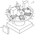
- the manufacturing apparatus 20 includes a base 21 and a rotary table 22 fixed on the base 21.
- the turntable 22 includes a disk-shaped top plate 22a that is rotated in a clockwise direction in a plan view (in the direction of an arrow in FIG. 2).
- a plurality of bases 30 having a rectangular plate shape are arranged side by side along the rotation direction of the top plate 22a.
- Base 30 As shown in FIG. 2, the base 30 is positioned with respect to the top plate 22a so that the long sides of the rectangle of the base 30 are along the radial direction of the top plate 22a.
- An engagement recess 31 having a rectangular shape in a bottom view for positioning the base 30 with respect to the top plate 22a is formed at the center of the lower surface of each base 30 (see FIG. 3).
- the six bases 30 are arranged at regular intervals, that is, at intervals of 60 degrees.
- each base 30 is rotated around the axis of the top plate 22a and conveyed.
- the rotation trajectory of each base 30 around the axis of the top plate 22a corresponds to the circulating conveyance path according to the present disclosure.
- the rotation direction of the top plate 22a may be referred to as the conveyance direction A of the base 30.
- the inner side and the outer side in the radial direction of the top plate 22a may be simply referred to as an inner side and an outer side.
- identification codes 32 indicating individual identification information given in advance to the base 30 are provided on both inner and outer side surfaces of each base 30.
- the identification code 32 is, for example, a barcode.
- a QR code registered trademark
- a coating device 41 used in the first step As shown in FIG. 2, above the top plate 22a, there are a coating device 41 used in the first step, a first heating device 42 used in the second step, and a first camera used in the first inspection step. 51, a printing device 43 used in the third step, a second heating device 44 used in the fourth step, and a second camera 52 used in the second inspection step.
- the coating device 41 is, for example, a die coater device, and forms a film 12 a having a rectangular shape in plan view by applying a dielectric elastomer raw material composition on the upper surface of the base 30 or the electrode layer 13.
- one film 12 a is formed by the coating apparatus 41.
- the first heating device 42 is, for example, a hot plate heating device, and forms the dielectric layer 12 by heating and curing the film 12a formed in the first step in a non-contact manner.
- the first camera 51 is a CCD camera, for example, and photographs the film 12a formed in the first process.
- the imaging result by the first camera 51 is output to the control device 60 in order to inspect the film 12a by image analysis.
- the printing device 43 is, for example, an ink jet printing device, and forms a film 13a having a rectangular shape in plan view by spraying a raw material composition of a conductive elastomer onto a predetermined range on the dielectric layer 12.
- one film 13 a is formed by the printing device 43.
- the second heating device 44 is, for example, a hot plate heating device, and forms the electrode layer 13 by heating and curing the film 13a formed in the third step in a non-contact manner.
- the second camera 52 is a CCD camera, for example, and photographs the film 13a formed in the third step.
- the imaging result obtained by the second camera 52 is output to the control device 60 in order to inspect the film 13a by image analysis.
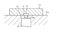
- the rotary table 22 is provided with a rotating device 23 that rotates each base 30 with respect to the top plate 22a.
- a rotary actuator 24 is provided on the top plate 22a.
- the rotary actuator 24 is an air cylinder, for example, and has a rotating shaft 24a protruding from the upper surface of the top plate 22a.
- An engaging portion 25 is connected to the tip of the rotating shaft 24a.
- the engaging portion 25 has a rectangular parallelepiped shape corresponding to the engaging recess 31 of the base 30.
- each base 30 has advanced to the first step, the second step, the first inspection step, the third step, the fourth step, and the second inspection step.
- a detection unit 61 for detecting the identification code 32 of the base 30 is provided for each process. In FIG. 2, only the detection unit 61 corresponding to the first step is illustrated.
- the control device 60 is a drive control process for the rotary table 22, a drive control process for the coating device 41, an energization control process for the first heating device 42, an imaging control process and an image analysis process for the first camera 51, and a drive control for the printing device 43. Processing, energization control processing of the second heating device 44, imaging control processing and image analysis processing of the second camera 52 are performed. Further, the control device 60 performs a drive control process for the rotation device 23. Further, the control device 60 derives the number of circulations of each base 30 based on the number of times detected by the detection unit 61.
- control device 60 Various control processes are performed by the control device 60 as follows. First, in a state where each base 30 is positioned by each engaging portion 25 and disposed on the top plate 22a, the first step is performed on the first base 30 positioned immediately below the coating device 41. .
- the turntable 22 is then rotated, so that the first base 30 moves to a position immediately below the first heating device 42. Then, the second step is performed on the first base 30. At this time, the first step is performed on the second base 30 that has moved directly below the coating device 41.
- the turntable 22 is then rotated, so that the first base 30 moves to a position directly below the first camera 51. Then, the first inspection process is performed on the first base 30.
- the first inspection step the presence / absence of chipping of the film 12a is determined by a known image analysis.
- the second step is performed on the second base 30 and the first step is performed on the third base 30.
- the turntable 22 is then rotated, so that the first base 30 moves to directly below the printing device 43. Then, the third step is performed on the first base 30. At this time, the first inspection process is performed on the second base 30 and the second process is performed on the third base 30. In addition, the first step is performed on the fourth base 30.
- the third step as shown in FIG. 5, when the number of circulations of the base 30 that is the target of the third step is an even number (see FIG. 5B), it is an odd number.
- the base 30 is rotated 180 degrees by the rotating device 23 (see FIG. 5A). Thereby, the formation range of the dielectric elastomer film 13a on the dielectric layer 12 is different from the formation range of the film 13a in the previous third step.
- the first base 30 moves to the position immediately below the second heating device 44 by rotating the turntable 22. Then, the fourth step is performed on the first base 30. At this time, the third step is performed on the second base 30 and the first inspection step is performed on the third base 30. In addition, the second step is performed on the fourth base 30 and the first step is performed on the fifth base 30.
- the first base 30 moves to a position immediately below the second camera 52 by rotating the turntable 22. Then, the second inspection process is performed on the first base 30.
- the second inspection step the presence / absence of chipping of the film 13a is determined by a known image analysis.
- the fourth step is performed on the second base 30 and the third step is performed on the third base 30.
- a first inspection process is performed on the fourth base 30 and a second process is performed on the fifth base 30.
- the first step is performed on the sixth base 30.
- the turntable 22 is then rotated, so that the first base 30 moves again to just below the coating device 41.
- the steps from the first step to the second inspection step described above are sequentially performed a plurality of times on the six bases 30.
- the base 30 on which the number of circulations reaches a predetermined number and the laminated body 10a is formed is taken out from the top plate 22a by a robot arm (not shown). Then, an additional heating step is performed on the stacked body 10 a formed on the base 30.
- the conductive elastomer film 13a can be formed on the dielectric elastomer film 12a in the middle of curing, and the conductive elastomer film 13a in the middle of curing can be formed.
- a film 12a made of dielectric elastomer can be formed thereon.
- the film 12a formed in the first step is inspected by image analysis (first inspection step). Further, after the fourth step, the film 13a formed in the third step is inspected by image analysis (second inspection step).
- the base 30 on which the film 12a is formed can be taken out from the top plate 22a before proceeding to the third step.
- the base 30 on which the film 13a is formed can be taken out from the top plate 22a before proceeding to the first step. For this reason, when the film
- the first inspection process is performed after the film 12a is heated in the second process
- the second inspection process is performed after the film 13a is heated in the fourth process.
- membrane 12a, 13a can be discovered by an inspection process being performed after a bubble generate
- the first step, the second step, the third step, the fourth step, the first inspection step, and the second inspection step are performed at different positions on the top plate 22a (conveyance path) of the rotary table 22. I made it.
- each process can be performed simultaneously. Thereby, the operating efficiency of each process equipment can be improved. Therefore, the time required for forming the stacked body 10a can be shortened.
- An individual identification code 32 is given in advance to each base 30, and when the base 30 passes through each detection unit 61, the detection code 61 of the base 30 passing therethrough is detected by the detection unit 61.
- the number of circulations of the base 30 is derived based on the number of detections by the detection unit 61.
- the number of circulations of the base 30 can be managed individually. For this reason, for example, the base 30 in which the formation failure of the film 12a (13a) occurs during the formation and lamination of the unit layer 11 is taken out from the top plate 22a of the turntable 22, and then the place where the base 30 is arranged Since the new base 30 is disposed in the base unit 11, the unit layer 11 can be formed and stacked in parallel with the other bases 30.
- the base 30 whose number of circulations has reached a predetermined number is taken out from the top plate 22 a of the rotary table 22. According to such a method, the base 30 in which the number of circulations reaches a predetermined number, that is, the base 30 on which the predetermined number of unit layers 11 are stacked and the stacked body 10a is formed can be reliably taken out from the top plate 22a. .
- An additional heating step is performed on the laminated body 10a formed on the base 30 taken out from the top plate 22a of the turntable 22 when the number of circulation reaches a predetermined number. .
- the printing device 43 forms the conductive elastomer film 13a over a predetermined range. Furthermore, in the third step, by rotating the base 30 that is the target of the third step, the formation range of the dielectric elastomer film 13a on the dielectric layer 12 formed on the base 30 is changed to the previous range. It was made to differ from the formation range of the film
- the formation range of two electrode layers 13 adjacent in the stacking direction of the stacked body 10a that is, the formation range of the positive electrode layer 13A and the negative electrode layer 13B can be easily made different. be able to.
- the rotary actuator 24 of the rotating device 23 is not limited to an air cylinder but may be an electric motor.
- the forming range of the dielectric elastomer film 13a on the dielectric layer 12 formed on the base 30 that is the target of the third step is changed by the printing device 43 to the film 13a in the previous third step. If it is made to differ from the formation range, the rotating device 23 can be omitted.
- an IC chip having individual identification information may be provided on each base 30. -You may make it perform a 1st test process between a 1st process and a 2nd process. Further, the second inspection step may be performed between the third step and the fourth step.
- the coating apparatus 41 used in the first step is not limited to the die coater apparatus, but may be an apparatus that applies a spray using a mask, for example.
- the same ink jet printing apparatus as in the third step may be used.
- a plurality of (for example, four) films 12a made of dielectric elastomer may be formed on one base 30.
- a conductive elastomer film 13a may be formed on each of the four dielectric layers 12 formed by curing each film 12a.
- the first heating device 42 used in the second step is not limited to the hot plate heating device, but may be an infrared heating device, for example. Further, heating means such as a heater may be provided on the base 30, and heating from above and heating from below may be used in combination.
- the second step is not limited to the step of heating and drying the film 12a, and can be appropriately changed according to the raw material composition. For example, the film 12a may be cured by ultraviolet irradiation. Moreover, the same change can be performed also about the 2nd heating apparatus 44 used in a 4th process.
- the third step is not limited to the step of forming the film 13a using the printing device 43, and the film 13a can also be formed by applying by spraying using a mask.
- route which circulates based on this indication is not limited to what is comprised using the rotary table 22, You may comprise the conveyance path
- a plurality of heating devices 42 and 44 for performing the second and fourth steps are provided.
- the base 30 may be transported by the transport mechanism between the heating devices 42 (44).
- the first conveyor 71 and the second conveyor 72 are arranged in parallel to each other.
- the 1st conveyor 71 conveys the base 30 toward the one side (right side of FIG. 8) of the longitudinal direction.
- the 2nd conveyor 72 conveys the base 30 toward the other side (left side of FIG. 8) of the longitudinal direction.
- the camera 52 is provided along the longitudinal direction of each conveyor 71 and 72 with those work tables.
- the short arrow shown in FIG. 8 has shown the conveyance mechanism or articulated robot which conveys the base 30 between the conveyors 71 and 72 and a work table, or between work tables.
Landscapes
- General Electrical Machinery Utilizing Piezoelectricity, Electrostriction Or Magnetostriction (AREA)
- Particle Formation And Scattering Control In Inkjet Printers (AREA)
Abstract
積層型誘電アクチュエータは、複数の単位層(11)が積層された積層体(10a)を有する。各単位層(11)は、誘電エラストマー製の誘電層(12)と、誘電層の一方の面に設けられた導電エラストマー製の電極層(13)とを備える。当該積層型誘電アクチュエータの製造方法は、誘電エラストマー製の膜(12a)を形成する第1工程と、誘電エラストマー製の膜(12a)を硬化させて誘電層(12)を形成する第2工程と、誘電層(12)上に導電エラストマー製の膜(13a)を形成する第3工程と、導電エラストマー製の膜(13a)を硬化させて電極層(13)を形成する第4工程と、を備える。当該製造方法では、循環する搬送経路上において搬送方向(A)に並んで配置された複数の基台(30)がそれぞれ循環される間に、複数の基台(30)上にて、第1工程から第4工程までを順に行うことをそれぞれ複数回繰り返すことにより各基台(30)上に積層体(10a)を形成する。
Description
本開示は、積層型誘電アクチュエータの製造方法に関する。
特許文献1には、複数の単位層により構成される積層型誘電アクチュエータ(以下、誘電アクチュエータと称す)の製造方法が開示されている。各単位層は、誘電エラストマー製の誘電層と、その誘電層上に設けられた電極層とを備えている。特許文献1に記載の製造方法では、1枚の誘電層上に複数の電極層を配置することにより中間品が形成される。そして、その中間品を電極層同士が重なるように折り畳むことによって誘電アクチュエータが製造される。
ところで、特許文献1に記載の製造方法の場合には、以下の不都合が生じる。すなわち、誘電層及び電極層はエラストマー製であり、かつそれらの厚さは数十μmと薄い。そのため、電極層同士が重なるように中間品を折り畳む際の取り扱いが難しいといった不都合や、電極層同士の位置合わせが難しいといった不都合が生じ、誘電アクチュエータの製造方法の機械化が困難である。
本開示の目的は、機械化を可能とした積層型誘電アクチュエータの製造方法を提供することにある。
上記目的を達成するための積層型誘電アクチュエータの製造方法は、複数の単位層が積層された積層体を有し、各単位層は、誘電エラストマー製の誘電層と、前記誘電層の一方の面に設けられた導電エラストマー製の電極層とを備える積層型誘電アクチュエータを製造する方法であって、前記誘電エラストマー製の膜を形成する第1工程と、前記誘電エラストマー製の前記膜を硬化させて前記誘電層を形成する第2工程と、前記誘電層上に前記導電エラストマー製の膜を形成する第3工程と、前記導電エラストマー製の前記膜を硬化させて前記電極層を形成する第4工程と、を備え、循環する搬送経路上において搬送方向に並んで配置された複数の基台がそれぞれ循環される間に、複数の前記基台上にて、前記第1工程から前記第4工程までを順に行うことをそれぞれ複数回繰り返すことにより各基台上に前記積層体を形成する。
同方法によれば、積層体を形成する各工程が基台上において行われるため、特許文献1に記載の製造方法に比べて、取り扱いが容易となり、機械化が可能となる。
また、上記方法によれば、硬化途中の状態における誘電エラストマー製の膜の上に導電エラストマー製の膜を形成することが可能となるとともに、硬化途中の状態における導電エラストマー製の膜の上に誘電エラストマー製の膜を形成することが可能となる。これにより、積層体の形成に要する時間を短縮することができる。
また、上記方法によれば、硬化途中の状態における誘電エラストマー製の膜の上に導電エラストマー製の膜を形成することが可能となるとともに、硬化途中の状態における導電エラストマー製の膜の上に誘電エラストマー製の膜を形成することが可能となる。これにより、積層体の形成に要する時間を短縮することができる。
上記積層型誘電アクチュエータの製造方法において、前記第1工程、前記第2工程、前記第3工程、及び前記第4工程を前記搬送経路上における互いに異なる位置にて行うことが好ましい。
同方法によれば、4つ以上の基台を搬送経路上に配置すれば、各工程を同時に行うことが可能となる。これにより、各工程設備の稼働効率を高めることができる。したがって、積層体の形成に要する時間を短縮することができる。
上記積層型誘電アクチュエータの製造方法において、前記第1工程と前記第3工程との間に行われ、前記第1工程により形成された前記膜の検査を行う第1検査工程と、前記第3工程と前記第1工程との間に行われ、前記第3工程により形成された前記膜の検査を行う第2検査工程と、を備えることが好ましい。
同方法によれば、第3工程までに、第1工程により形成された膜の検査が行われる。このため、第1工程において形成された膜が不良であった場合に、当該膜が形成された基台を第3工程に進む前に搬送経路から取り出すことが可能となる。また、第1工程までに、第3工程により形成された膜の検査が行われる。このため、第3工程において形成された膜が不良であった場合に、当該膜が形成された基台を第1工程に進む前に搬送経路から取り出すことが可能となる。このため、直前に形成された膜に不良があった場合に、その後の無駄な膜の形成を抑制することができる。
上記積層型誘電アクチュエータの製造方法において、前記第1検査工程及び前記第2検査工程の各々は、画像解析による検査を行う工程であり、前記第2工程の後に前記第1検査工程を行うとともに、前記第4工程の後に前記第2検査工程を行うことが好ましい。
第1検査工程及び第2検査工程において画像解析により膜の検査を行う場合、膜の表面に溶剤が存在する場合などには、ハレーションが生じやすく、検査精度が悪化するおそれがある。また、第2及び第4工程において膜を硬化させる際に、膜から気泡が発生することで膜に不良が発生するおそれがある。
この点、上記方法によれば、第2工程において膜が硬化された後に第1検査工程が行われるとともに、第4工程において膜が硬化された後に第2検査工程が行われる。このため、膜の表面から溶剤が除去された後に検査工程が行われることで、上述したハレーションの発生を抑制することができ、検査精度の悪化を抑制することができる。また、膜から気泡が発生した後に検査工程が行われることで、膜の不良を発見することができる。
上記積層型誘電アクチュエータの製造方法において、各基台に対して個別の識別情報を予め付与し、各基台が前記搬送経路の所定位置を通過する際に、その基台の前記識別情報を検出部により検出し、前記検出部による検出回数に基づいてその基台の循環回数を導出することが好ましい。
同方法によれば、基台の循環回数を個別に管理することができるため、例えば単位層の形成及び積層途中において膜の形成不良が発生した基台を搬送経路から取り出し、その後、当該基台の配置されていた箇所に新たな基台を配置することで、単位層の形成及び積層を、他の基台と並行して行うことができる。
上記積層型誘電アクチュエータの製造方法において、前記循環回数が所定の数に達した基材を前記搬送経路から取り出すことが好ましい。
同方法によれば、循環回数が所定の数に達した基台、すなわち単位層が所定数積層されて積層体が形成された基台を搬送経路から確実に取り出すことができる。
同方法によれば、循環回数が所定の数に達した基台、すなわち単位層が所定数積層されて積層体が形成された基台を搬送経路から確実に取り出すことができる。
上記積層型誘電アクチュエータの製造方法において、前記循環回数が前記所定の数に達して前記搬送経路から取り出された前記基台上に形成された前記積層体に対して追加の硬化工程を行うことが好ましい。
同方法によれば、循環回数が所定の数に達して搬送経路から取り出された基台上の積層体を更に硬化させることができる。このため、第2工程及び第4工程においては、第3工程または第1工程を行うことのできる程度の短い硬化時間で済む。したがって、積層体の形成に要する時間を短縮することができる。
上記積層型誘電アクチュエータの製造方法において、前記第3工程において、当該第3工程の対象となる基台上に形成された前記誘電層に対する前記誘電エラストマー製の膜の形成範囲を、前回の前記第3工程における前記膜の形成範囲と異ならせることが好ましい。
同方法によれば、積層体の積層方向において隣り合う2つの電極層の形成範囲、すなわち正極層と負極層との形成範囲を異ならせることができる。
上記積層型誘電アクチュエータの製造方法において、前記第3工程において、当該第3工程の対象となる基台を回転させることにより、前記膜の形成範囲を、前回の前記第3工程における前記膜の形成範囲と異ならせることが好ましい。
上記積層型誘電アクチュエータの製造方法において、前記第3工程において、当該第3工程の対象となる基台を回転させることにより、前記膜の形成範囲を、前回の前記第3工程における前記膜の形成範囲と異ならせることが好ましい。
同方法によれば、基台を回転させることにより、積層体の積層方向において隣り合う2つの電極層の形成範囲、すなわち正極層と負極層との形成範囲を容易に異ならせることができる。
本開示によれば、積層型誘電アクチュエータの製造方法の機械化が可能となる。
以下、図1~図6を参照して、積層型誘電アクチュエータの製造方法の一実施形態について説明する。
まず、本実施形態の積層型誘電アクチュエータ(以下、誘電アクチュエータ10と称す)について説明する。
まず、本実施形態の積層型誘電アクチュエータ(以下、誘電アクチュエータ10と称す)について説明する。
図1に示すように、誘電アクチュエータ10は、その厚さ方向に積層された複数の単位層11により構成された積層体10aを有している。積層体10aは、複数の単位層11として、複数の第1単位層11Aと複数の第2単位層11Bとを備えている。第1単位層11Aと第2単位層11Bとは交互に配置されている。
第1単位層11Aは、誘電エラストマー製の誘電層12を備えている。誘電層12は、その厚さが例えば、20~200μmである薄膜状に形成されている。
誘電層12を構成する誘電エラストマーは特に限定されるものではなく、公知の誘電アクチュエータに用いられる誘電エラストマーを用いることができる。上記誘電エラストマーとしては、例えば、架橋ポリロタキサン、シリコーンエラストマー、アクリルエラストマー、及びウレタンエラストマーが挙げられる。これら誘電エラストマーのうちの一種を用いてもよいし、複数種を併用してもよい。
誘電層12を構成する誘電エラストマーは特に限定されるものではなく、公知の誘電アクチュエータに用いられる誘電エラストマーを用いることができる。上記誘電エラストマーとしては、例えば、架橋ポリロタキサン、シリコーンエラストマー、アクリルエラストマー、及びウレタンエラストマーが挙げられる。これら誘電エラストマーのうちの一種を用いてもよいし、複数種を併用してもよい。
誘電層12の一方の面(図1の上面)の中央部には、導電エラストマー製の電極層13が配置されている。電極層13は、その厚さが例えば、10~100μmである薄膜状に形成されている。
電極層13を構成する導電エラストマーは特に限定されるものではなく、公知の誘電アクチュエータに用いられる導電エラストマーを用いることができる。上記導電エラストマーとしては、例えば、絶縁性高分子及び導電性フィラーを含有する導電エラストマーが挙げられる。
上記絶縁性高分子としては、例えば、ポリロタキサン、シリコーンエラストマー、アクリルエラストマー、及びウレタンエラストマーが挙げられる。これら絶縁性高分子のうちの一種を用いてもよいし、複数種を併用してもよい。
上記導電性フィラーとしては、例えば、ケッチェンブラック(登録商標)、カーボンブラック、及び金属粒子が挙げられる。金属粒子としては、例えば、銅及び銀が挙げられる。これら導電性フィラーのうちの一種を用いてもよいし、複数種を併用してもよい。
図1に示すように、第1単位層11Aでは、誘電層12の一方の面(図1の上面)の中央部における特定方向の一方側(図1の左側)に寄った位置に、電極層13(正極層13A)が配置され、電極層13(正極層13A)の周囲に誘電層12が配置されている。
第2単位層11Bの構成は、電極層13及び電極層13の周囲を囲む誘電層12の配置が異なる点を除いて、第1単位層11Aの構成と同じである。すなわち、第2単位層11Bでは、誘電層12の一方の面(図1の上面)の中央部における特定方向の他方側(図1の右側)に寄った位置に電極層13(負極層13B)が配置され、電極層13(負極層13B)の周囲に誘電層12が配置されている。
そして、上記の第1単位層11A及び第2単位層11Bが交互に配置されることにより、隣り合う電極層13同士の間に誘電層12が配置された誘電アクチュエータ10が構成される。単位層11の積層数は特に限定されるものではないが、例えば、第1単位層11A及び第2単位層11Bの合計数が5~1000層である。
また、最下部に配置された第1単位層11Aの下には、誘電層12が設けられている。
次に、図6を参照して、誘電アクチュエータ10の積層体10aの製造方法について説明する。積層体10aは、誘電エラストマー製の膜12aを形成する第1工程、同膜12aを硬化させて誘電層12を形成する第2工程、誘電層12上に導電エラストマー製の膜13aを形成する第3工程、及び同膜13aを硬化させて電極層13を形成する第4工程を順に行うことを複数回繰り返すことにより形成される。
次に、図6を参照して、誘電アクチュエータ10の積層体10aの製造方法について説明する。積層体10aは、誘電エラストマー製の膜12aを形成する第1工程、同膜12aを硬化させて誘電層12を形成する第2工程、誘電層12上に導電エラストマー製の膜13aを形成する第3工程、及び同膜13aを硬化させて電極層13を形成する第4工程を順に行うことを複数回繰り返すことにより形成される。
(第1工程)
図6に示すように、先ず、基台30(図2~図5参照)の上面に、低粘度の誘電エラストマーの原料組成物を塗布することにより膜12aを形成する。本実施形態の原料組成物には、溶剤が含まれている。なお、図6では基台30の図示を省略している。
図6に示すように、先ず、基台30(図2~図5参照)の上面に、低粘度の誘電エラストマーの原料組成物を塗布することにより膜12aを形成する。本実施形態の原料組成物には、溶剤が含まれている。なお、図6では基台30の図示を省略している。
(第2工程)
次に、膜12aに対して硬化処理を施すことにより、最外層に位置する誘電層12を形成する。
次に、膜12aに対して硬化処理を施すことにより、最外層に位置する誘電層12を形成する。
(第3工程)
次に、先に形成された誘電層12の上面の一部に、低粘度の導電エラストマーの原料組成物を部分的に印刷することにより膜13aを形成する。本実施形態の原料組成物には、溶剤が含まれている。このとき、誘電層12の上面のうち電極層13の周囲には、誘電層12が露出する露出部分12cが設けられる。
次に、先に形成された誘電層12の上面の一部に、低粘度の導電エラストマーの原料組成物を部分的に印刷することにより膜13aを形成する。本実施形態の原料組成物には、溶剤が含まれている。このとき、誘電層12の上面のうち電極層13の周囲には、誘電層12が露出する露出部分12cが設けられる。
(第4工程)
次に、膜13aに対して硬化処理を施すことにより、導電エラストマー製の電極層13を形成する。
次に、膜13aに対して硬化処理を施すことにより、導電エラストマー製の電極層13を形成する。
次に、第1工程を行う、すなわち、電極層13の上部、及び電極層13の下側に位置する誘電層12の露出部分12cの上部を覆うように誘電エラストマーの原料組成物を塗布することにより膜12aを形成する。このとき、塗布された原料組成物は、自身の流動性に基づいて、その上面が水平に近づくようにレベリングされて、電極層13に塗布された部分の上面と、露出部分12cに塗布された部分の上面との段差が小さくなる。
次に、第2工程を行う、すなわち、膜12aに対して硬化処理を施すことにより、誘電層12を形成する。これにより、最下部に位置する単位層11が形成される。
その後、第3工程、第4工程、第1工程、及び第2工程を順に行うことにより、各々が誘電層12と電極層13とを備える複数の単位層11が形成される。
その後、第3工程、第4工程、第1工程、及び第2工程を順に行うことにより、各々が誘電層12と電極層13とを備える複数の単位層11が形成される。
詳しくは、第2工程を経て形成された単位層11の上面を構成する誘電層12を、先に形成された誘電層12として、第3工程、第4工程、第1工程、及び第2工程を順に行うことにより、新たな単位層11が、先に形成された単位層11の上に接合した状態で形成される。
このとき、先に形成された単位層11が第1単位層11Aである場合、新たな単位層11として第2単位層11Bが形成されるように、電極層13の形成位置を調整する。また、先に形成された単位層11が第2単位層11Bである場合、新たな単位層11として第1単位層11Aが形成されるように、電極層13の形成位置を調整する。
そして、単位層11の積層数が所定の数となるまで、第3工程、第4工程、第1工程、及び第2工程を順に繰り返し行うことにより、複数の単位層11が積層された積層体10aが得られる。
次に、図2~図5を参照して、本実施形態における誘電アクチュエータ10の積層体10aを製造する製造装置20について説明する。
図2に示すように、製造装置20は、ベース21と、そのベース21の上に固定された回転テーブル22とを備えている。回転テーブル22は、平面視時計回り方向(図2中の矢印方向)に回転される円盤状の天板22aを備えている。
図2に示すように、製造装置20は、ベース21と、そのベース21の上に固定された回転テーブル22とを備えている。回転テーブル22は、平面視時計回り方向(図2中の矢印方向)に回転される円盤状の天板22aを備えている。
回転テーブル22の天板22aの上には、長方形板状をなす複数の基台30が、天板22aの回転方向に沿って並んで配置されている。
(基台30)
図2に示すように、基台30の長方形の長辺が天板22aの径方向に沿うようにして天板22aに対して基台30が位置決めされている。各基台30の下面の中央部には、その基台30を天板22aに対して位置決めするための下面視長方形状の係合凹部31が形成されている(図3参照)。
(基台30)
図2に示すように、基台30の長方形の長辺が天板22aの径方向に沿うようにして天板22aに対して基台30が位置決めされている。各基台30の下面の中央部には、その基台30を天板22aに対して位置決めするための下面視長方形状の係合凹部31が形成されている(図3参照)。
本実施形態では、6つの基台30が等間隔、すなわち60度間隔にて配置されている。回転テーブル22の天板22aが回転すると、各基台30は、天板22aの軸線を中心に回転されて搬送される。ここで、天板22aの軸線を中心とする各基台30の回転軌跡が、本開示に係る循環する搬送経路に相当する。以降において、天板22aの回転方向を、基台30の搬送方向Aと称することがある。また、天板22aの径方向における内側及び外側を単に内側及び外側と称することがある。
図2及び図3に示すように、各基台30の内側及び外側の両側面には、基台30に対して予め付与された個別の識別情報を示す識別コード32が設けられている。識別コード32は、例えばバーコードである。なお、識別コード32としてQRコード(登録商標)を採用してもよい。
図2に示すように、天板22aの上方には、第1工程にて用いられる塗布装置41、第2工程にて用いられる第1加熱装置42、第1検査工程にて用いられる第1カメラ51、第3工程にて用いられる印刷装置43、第4工程にて用いられる第2加熱装置44、及び第2検査工程にて用いられる第2カメラ52が設けられている。
(塗布装置41)
塗布装置41は、例えばダイコータ装置であり、誘電エラストマーの原料組成物を基台30の上面または電極層13上に塗布することで平面視長方形状の膜12aを形成する。本実施形態では、塗布装置41により1つの膜12aを形成する。
塗布装置41は、例えばダイコータ装置であり、誘電エラストマーの原料組成物を基台30の上面または電極層13上に塗布することで平面視長方形状の膜12aを形成する。本実施形態では、塗布装置41により1つの膜12aを形成する。
(第1加熱装置42)
第1加熱装置42は、例えば熱板加熱装置であり、第1工程において形成された膜12aを非接触にて加熱して硬化させることで誘電層12を形成する。
第1加熱装置42は、例えば熱板加熱装置であり、第1工程において形成された膜12aを非接触にて加熱して硬化させることで誘電層12を形成する。
(第1カメラ51)
第1カメラ51は、例えばCCDカメラであり、第1工程において形成された膜12aを撮影する。第1カメラ51による撮影結果は、画像解析による膜12aの検査を行うために制御装置60に対して出力される。
第1カメラ51は、例えばCCDカメラであり、第1工程において形成された膜12aを撮影する。第1カメラ51による撮影結果は、画像解析による膜12aの検査を行うために制御装置60に対して出力される。
(印刷装置43)
印刷装置43は、例えばインクジェット印刷装置であり、導電エラストマーの原料組成物を誘電層12上の所定の範囲に噴射することで平面視長方形状の膜13aを形成する。本実施形態では、印刷装置43により1つの膜13aを形成する。
印刷装置43は、例えばインクジェット印刷装置であり、導電エラストマーの原料組成物を誘電層12上の所定の範囲に噴射することで平面視長方形状の膜13aを形成する。本実施形態では、印刷装置43により1つの膜13aを形成する。
(第2加熱装置44)
第2加熱装置44は、例えば熱板加熱装置であり、第3工程において形成された膜13aを非接触にて加熱して硬化させることで電極層13を形成する。
第2加熱装置44は、例えば熱板加熱装置であり、第3工程において形成された膜13aを非接触にて加熱して硬化させることで電極層13を形成する。
(第2カメラ52)
第2カメラ52は、例えばCCDカメラであり、第3工程において形成された膜13aを撮影する。第2カメラ52による撮影結果は、画像解析による膜13aの検査を行うために制御装置60に対して出力される。
第2カメラ52は、例えばCCDカメラであり、第3工程において形成された膜13aを撮影する。第2カメラ52による撮影結果は、画像解析による膜13aの検査を行うために制御装置60に対して出力される。
(回転装置23)
図3及び図4に示すように、回転テーブル22には、天板22aに対して各基台30を回転させる回転装置23が設けられている。
図3及び図4に示すように、回転テーブル22には、天板22aに対して各基台30を回転させる回転装置23が設けられている。
図4に示すように、天板22aには、ロータリアクチュエータ24が設けられている。ロータリアクチュエータ24は、例えばエアシリンダであり、天板22aの上面から突出する回転軸24aを有している。回転軸24aの先端には、係合部25が連結されている。係合部25は、基台30の係合凹部31に対応した直方体状をなしている。基台30の係合凹部31が係合部25に相対変位不能に係合されることにより、天板22aに対して基台30が位置決めされる。
(検出部61)
図2に示すように、天板22aの周囲には、各基台30が、第1工程、第2工程、第1検査工程、第3工程、第4工程、及び第2検査工程に進んだ際に、その基台30の識別コード32を検出する検出部61が工程毎に設けられている。なお、図2では、第1工程に対応する検出部61のみを図示している。
図2に示すように、天板22aの周囲には、各基台30が、第1工程、第2工程、第1検査工程、第3工程、第4工程、及び第2検査工程に進んだ際に、その基台30の識別コード32を検出する検出部61が工程毎に設けられている。なお、図2では、第1工程に対応する検出部61のみを図示している。
(制御装置60)
制御装置60は、回転テーブル22の駆動制御処理、塗布装置41の駆動制御処理、第1加熱装置42の通電制御処理、第1カメラ51の撮影制御処理及び画像解析処理、印刷装置43の駆動制御処理、第2加熱装置44の通電制御処理、並びに第2カメラ52の撮影制御処理及び画像解析処理を行う。また、制御装置60は、回転装置23の駆動制御処理を行う。また、制御装置60は、検出部61による検出回数に基づいて各基台30の循環回数を導出する。
制御装置60は、回転テーブル22の駆動制御処理、塗布装置41の駆動制御処理、第1加熱装置42の通電制御処理、第1カメラ51の撮影制御処理及び画像解析処理、印刷装置43の駆動制御処理、第2加熱装置44の通電制御処理、並びに第2カメラ52の撮影制御処理及び画像解析処理を行う。また、制御装置60は、回転装置23の駆動制御処理を行う。また、制御装置60は、検出部61による検出回数に基づいて各基台30の循環回数を導出する。
各種制御処理は、制御装置60により以下のように行われる。
まず、各基台30が各係合部25により位置決めされて天板22a上に配置された状態において、塗布装置41の直下に位置する1番目の基台30に対して第1工程が行われる。
まず、各基台30が各係合部25により位置決めされて天板22a上に配置された状態において、塗布装置41の直下に位置する1番目の基台30に対して第1工程が行われる。
第1工程が完了すると、次に、回転テーブル22が回転されることで、1番目の基台30は、第1加熱装置42の直下まで移動する。そして、1番目の基台30に対して第2工程が行われる。またこのとき、塗布装置41の直下に移動した2番目の基台30に対して第1工程が行われる。
第2工程が完了すると、次に、回転テーブル22が回転されることで、1番目の基台30は、第1カメラ51の直下まで移動する。そして、1番目の基台30に対して第1検査工程が行われる。ここで、第1検査工程では、膜12aの欠けの有無を周知の画像解析により判定する。またこのとき、2番目の基台30に対して第2工程が行われるとともに、3番目の基台30に対して第1工程が行われる。
第1検査工程が完了すると、次に、回転テーブル22が回転されることで、1番目の基台30は、印刷装置43の直下まで移動する。そして、1番目の基台30に対して第3工程が行われる。またこのとき、2番目の基台30に対して第1検査工程が行われるとともに、3番目の基台30に対して第2工程が行われる。また、4番目の基台30に対して第1工程が行われる。
ここで、第3工程においては、図5に示すように、当該第3工程の対象となる基台30の循環回数が偶数である場合(図5(b)参照)には、奇数である場合(図5(a)参照)に対して、回転装置23により基台30が180度回転される。これにより、誘電層12に対する誘電エラストマー製の膜13aの形成範囲が、前回の第3工程における膜13aの形成範囲と異なることとなる。
第3工程が完了すると、次に、回転テーブル22が回転されることで、1番目の基台30は、第2加熱装置44の直下まで移動する。そして、1番目の基台30に対して第4工程が行われる。またこのとき、2番目の基台30に対して第3工程が行われるとともに、3番目の基台30に対して第1検査工程が行われる。また、4番目の基台30に対して第2工程が行われるとともに、5番目の基台30に対して第1工程が行われる。
第4工程が完了すると、次に、回転テーブル22が回転されることで、1番目の基台30は、第2カメラ52の直下まで移動する。そして、1番目の基台30に対して第2検査工程が行われる。ここで、第2検査工程では、膜13aの欠けの有無を周知の画像解析により判定する。またこのとき、2番目の基台30に対して第4工程が行われるとともに、3番目の基台30に対して第3工程が行われる。また、4番目の基台30に対して第1検査工程が行われるとともに、5番目の基台30に対して第2工程が行われる。また、6番目の基台30に対して第1工程が行われる。
第2検査工程が完了すると、次に、回転テーブル22が回転されることで、1番目の基台30は、再び塗布装置41の直下まで移動する。
このようにして、6つの基台30上にて、上述した第1工程から第2検査工程までを順に行うことをそれぞれ複数回繰り返す。
このようにして、6つの基台30上にて、上述した第1工程から第2検査工程までを順に行うことをそれぞれ複数回繰り返す。
循環回数が所定の数に達して積層体10aが形成された基台30は、図示しないロボットアームによって天板22aから取り出される。そして、当該基台30上に形成された積層体10aに対して追加の加熱工程が行われる。
次に、本実施形態の作用効果について説明する。
(1)回転テーブル22の天板22a上において天板22aの回転方向(搬送方向A)に並んで配置された複数の基台30がそれぞれ循環される間に、複数の基台30上にて、第1工程から第4工程までを順に行うことをそれぞれ複数回繰り返すことにより各基台30上に積層体10aが形成される。
(1)回転テーブル22の天板22a上において天板22aの回転方向(搬送方向A)に並んで配置された複数の基台30がそれぞれ循環される間に、複数の基台30上にて、第1工程から第4工程までを順に行うことをそれぞれ複数回繰り返すことにより各基台30上に積層体10aが形成される。
こうした方法によれば、積層体10aを形成する各工程が基台30上において行われるため、特許文献1に記載の製造方法に比べて、取り扱いが容易となり、機械化が可能となる。
また、上記方法によれば、硬化途中の状態における誘電エラストマー製の膜12aの上に導電エラストマー製の膜13aを形成することが可能となるとともに、硬化途中の状態における導電エラストマー製の膜13aの上に誘電エラストマー製の膜12aを形成することが可能となる。これにより、積層体10aの形成に要する時間を短縮することができる。
(2)第2工程の後に、画像解析により、第1工程により形成された膜12aの検査を行うようにした(第1検査工程)。また、第4工程の後に、画像解析により、第3工程により形成された膜13aの検査を行うようにした(第2検査工程)。
こうした方法によれば、第1工程において形成された膜12aが不良であった場合に、当該膜12aが形成された基台30を第3工程に進む前に天板22aから取り出すことが可能となる。また、第3工程において形成された膜13aが不良であった場合に、当該膜13aが形成された基台30を第1工程に進む前に天板22aから取り出すことが可能となる。このため、直前に形成された膜12a,13aに不良があった場合に、その後の無駄な膜13a,12aの形成を抑制することができる。
ところで、カメラ51,52による撮影の際に、当該膜12a,13aの表面に残存する溶剤によってハレーションが生じやすく、検査精度が悪化するおそれがある。また、第2及び第4工程において膜12a,13aを加熱して硬化させる際に、気泡が発生することで膜12a,13aに不良が発生するおそれがある。
この点、本実施形態によれば、第2工程において膜12aが加熱された後に第1検査工程が行われるとともに、第4工程において膜13aが加熱された後に第2検査工程が行われる。このため、当該膜12a,13aの表面から溶剤が除去された後に検査工程が行われることで、上述したハレーションの発生を抑制することができ、検査精度の悪化を抑制することができる。また、膜12a,13aから気泡が発生した後に検査工程が行われることで、膜12a,13aの不良を発見することができる。
(3)第1工程、第2工程、第3工程、第4工程、第1検査工程、及び第2検査工程を回転テーブル22の天板22a(搬送経路)上における互いに異なる位置にて行うようにした。
こうした方法によれば、各工程を同時に行うことが可能となる。これにより、各工程設備の稼働効率を高めることができる。したがって、積層体10aの形成に要する時間を短縮することができる。
(4)各基台30に対して個別の識別コード32を予め付与し、各検出部61を基台30が通過する際に、その通過する基台30の識別コード32を検出部61により検出し、検出部61による検出回数に基づいて当該基台30の循環回数を導出するようにした。
こうした方法によれば、基台30の循環回数を個別に管理することができる。このため、例えば単位層11の形成及び積層途中において膜12a(13a)の形成不良が発生した基台30を回転テーブル22の天板22aから取り出し、その後、当該基台30の配置されていた箇所に新たな基台30を配置することで、単位層11の形成及び積層を、他の基台30と並行して行うことができる。
(5)循環回数が所定の数に達した基台30を回転テーブル22の天板22aから取り出すようにした。
こうした方法によれば、循環回数が所定の数に達した基台30、すなわち単位層11が所定数積層されて積層体10aが形成された基台30を天板22aから確実に取り出すことができる。
こうした方法によれば、循環回数が所定の数に達した基台30、すなわち単位層11が所定数積層されて積層体10aが形成された基台30を天板22aから確実に取り出すことができる。
(6)循環回数が所定の数に達して回転テーブル22の天板22aから取り出された基台30上に形成された積層体10aに対して追加の加熱工程(硬化工程)を行うようにした。
こうした方法によれば、循環回数が所定の数に達して搬送経路から取り出された基台30上の積層体10aを更に硬化させることができる。このため、第2工程及び第4工程においては、第3工程または第1工程を行うことのできる程度の短い加熱(硬化)時間で済む。したがって、積層体10aの形成に要する時間を短縮することができる。
(7)第3工程では、印刷装置43により所定の範囲に対して導電性エラストマー製の膜13aを形成する。さらに、第3工程では、当該第3工程の対象となる基台30を回転させることにより、当該基台30上に形成された誘電層12に対する誘電エラストマー製の膜13aの形成範囲を、前回の第3工程における膜13aの形成範囲と異ならせるようにした。
こうした方法によれば、基台30を回転させることにより、積層体10aの積層方向において隣り合う2つの電極層13の形成範囲、すなわち正極層13Aと負極層13Bとの形成範囲を容易に異ならせることができる。
本実施形態は、以下のように変更して実施することができる。本実施形態及び以下の変更例は、技術的に矛盾しない範囲で互いに組み合わせて実施することができる。
・回転装置23のロータリアクチュエータ24はエアシリンダに限定されず、電動モータであってもよい。
・回転装置23のロータリアクチュエータ24はエアシリンダに限定されず、電動モータであってもよい。
・第3工程において、印刷装置43によって、当該第3工程の対象となる基台30上に形成された誘電層12に対する誘電エラストマー製の膜13aの形成範囲を、前回の第3工程における膜13aの形成範囲と異ならせるようにすれば、回転装置23を省略することができる。
・積層体10aが完全に硬化しているのであれば、回転テーブル22の天板22a上から取り出された基台30上に形成された積層体10aに対して行われる追加の硬化工程を省略してもよい。
・バーコードやQRコードなどの識別コード32に代えて、各基台30に個別の識別情報を有するICチップを設けるようにしてもよい。
・第1検査工程を第1工程と第2工程との間に行うようにしてもよい。また、第2検査工程を第3工程と第4工程との間に行うようにしてもよい。
・第1検査工程を第1工程と第2工程との間に行うようにしてもよい。また、第2検査工程を第3工程と第4工程との間に行うようにしてもよい。
・第1及び第2検査工程を省略してもよい。
・第1工程において用いられる塗布装置41は、ダイコータ装置に限定されず、他に例えば、マスクを用いてスプレー等により塗布する装置であってもよい。また、第1工程において、第3工程と同様なインクジェット印刷装置を用いてもよい。
・第1工程において用いられる塗布装置41は、ダイコータ装置に限定されず、他に例えば、マスクを用いてスプレー等により塗布する装置であってもよい。また、第1工程において、第3工程と同様なインクジェット印刷装置を用いてもよい。
・図7に示すように、1つの基台30上に誘電エラストマー製の複数(例えば4つ)の膜12aを形成するようにしてもよい。この場合、各膜12aを硬化して形成された4つの誘電層12上に導電エラストマー製の膜13aをそれぞれ形成すればよい。
・第2工程において用いられる第1加熱装置42は熱板加熱装置に限定されず、他に例えば赤外線加熱装置であってもよい。また、基台30にヒータ等の加熱手段を設け、上方からの加熱と下方からの加熱とを併用してもよい。第2工程は、膜12aを加熱乾燥させて硬化させる工程に限定されず、原料組成物に応じて適宜変更することができる。例えば、紫外線照射により膜12aを硬化させるようにしてもよい。また、第4工程において用いられる第2加熱装置44についても同様な変更を行うことができる。
・第3工程は、印刷装置43を用いて膜13aを形成する工程に限定されず、マスクを用いてスプレー等により塗布して膜13aを形成することもできる。
・本開示に係る循環する搬送経路は、回転テーブル22を用いて構成されるものに限定されず、他に例えば、コンベアなどを用いて循環する搬送経路を構成してもよい。また、膜12a,13aをそれぞれ硬化させる第2及び4工程に要する時間が他の工程に要する時間に比べて長い場合には、第2及び4工程を行う加熱装置42,44を複数設け、複数の加熱装置42(44)間において基台30を搬送機構により搬送するようにすればよい。
・本開示に係る循環する搬送経路は、回転テーブル22を用いて構成されるものに限定されず、他に例えば、コンベアなどを用いて循環する搬送経路を構成してもよい。また、膜12a,13aをそれぞれ硬化させる第2及び4工程に要する時間が他の工程に要する時間に比べて長い場合には、第2及び4工程を行う加熱装置42,44を複数設け、複数の加熱装置42(44)間において基台30を搬送機構により搬送するようにすればよい。
図8に示す変更例では、第1コンベア71と第2コンベア72とが互いに平行に配置されている。第1コンベア71は、その長手方向の一方の側(図8の右側)に向けて基台30を搬送する。また、第2コンベア72は、その長手方向の他方の側(図8の左側)に向けて基台30を搬送する。ここで、第1コンベア71と第2コンベア72との間には、塗布装置41、2つの第1加熱装置42、第1カメラ51、印刷装置43、2つの第2加熱装置44、及び第2カメラ52がそれらの作業台と共に各コンベア71,72の長手方向に沿って設けられている。また、図8に示す短い矢印は、コンベア71,72と作業台との間、あるいは作業台間において基台30を搬送する搬送機構または多関節ロボットを示している。
10…誘電アクチュエータ、10a…積層体、11…単位層、11A…第1単位層、11B…第2単位層、12…誘電層、12a…膜、12c…露出部分、13…電極層、13A…正極層、13B…負極層、13a…膜、20…製造装置、21…ベース、22…回転テーブル、22a…天板、23…回転装置、24…ロータリアクチュエータ、24a…回転軸、25…係合部、30…基台、31…係合凹部、32…識別コード、41…塗布装置、42…第1加熱装置、42a…熱板、43…印刷装置、44…第2加熱装置、44a…熱板、51…第1カメラ、52…第2カメラ、60…制御装置、61…検出部、71,72…コンベア。
Claims (9)
- 複数の単位層が積層された積層体を有し、各単位層は、誘電エラストマー製の誘電層と、前記誘電層の一方の面に設けられた導電エラストマー製の電極層とを備える積層型誘電アクチュエータを製造する方法であって、
前記誘電エラストマー製の膜を形成する第1工程と、
前記誘電エラストマー製の前記膜を硬化させて前記誘電層を形成する第2工程と、
前記誘電層上に前記導電エラストマー製の膜を形成する第3工程と、
前記導電エラストマー製の前記膜を硬化させて前記電極層を形成する第4工程と、を備え、
循環する搬送経路上において搬送方向に並んで配置された複数の基台がそれぞれ循環される間に、複数の前記基台上にて、前記第1工程から前記第4工程までを順に行うことをそれぞれ複数回繰り返すことにより各基台上に前記積層体を形成する、
積層型誘電アクチュエータの製造方法。 - 前記第1工程、前記第2工程、前記第3工程、及び前記第4工程を前記搬送経路上における互いに異なる位置にて行う、
請求項1に記載の積層型誘電アクチュエータの製造方法。 - 前記第1工程と前記第3工程との間に行われ、前記第1工程により形成された前記膜の検査を行う第1検査工程と、
前記第3工程と前記第1工程との間に行われ、前記第3工程により形成された前記膜の検査を行う第2検査工程と、を備える、
請求項1または請求項2に記載の積層型誘電アクチュエータの製造方法。 - 前記第1検査工程及び前記第2検査工程の各々は、画像解析による検査を行う工程であり、
前記第2工程の後に前記第1検査工程を行うとともに、前記第4工程の後に前記第2検査工程を行う、
請求項3に記載の積層型誘電アクチュエータの製造方法。 - 各基台に対して個別の識別情報を予め付与し、各基台が前記搬送経路の所定位置を通過する際に、その基台の前記識別情報を検出部により検出し、前記検出部による検出回数に基づいてその基台の循環回数を導出する、
請求項1~請求項4のいずれか一項に記載の積層型誘電アクチュエータの製造方法。 - 前記循環回数が所定の数に達した基材を前記搬送経路から取り出す、
請求項5に記載の積層型誘電アクチュエータの製造方法。 - 前記循環回数が前記所定の数に達して前記搬送経路から取り出された前記基台上に形成された前記積層体に対して追加の硬化工程を行う、
請求項6に記載の積層型誘電アクチュエータの製造方法。 - 前記第3工程において、当該第3工程の対象となる基台上に形成された前記誘電層に対する前記誘電エラストマー製の膜の形成範囲を、前回の前記第3工程における前記膜の形成範囲と異ならせる、
請求項1~請求項7のいずれか一項に記載の積層型誘電アクチュエータの製造方法。 - 前記第3工程において、当該第3工程の対象となる基台を回転させることにより、前記膜の形成範囲を、前回の前記第3工程における前記膜の形成範囲と異ならせる、
請求項8に記載の積層型誘電アクチュエータの製造方法。
Applications Claiming Priority (2)
| Application Number | Priority Date | Filing Date | Title |
|---|---|---|---|
| JP2018077072A JP2019187143A (ja) | 2018-04-12 | 2018-04-12 | 積層型誘電アクチュエータの製造方法 |
| JP2018-077072 | 2018-04-12 |
Publications (1)
| Publication Number | Publication Date |
|---|---|
| WO2019198650A1 true WO2019198650A1 (ja) | 2019-10-17 |
Family
ID=68164013
Family Applications (1)
| Application Number | Title | Priority Date | Filing Date |
|---|---|---|---|
| PCT/JP2019/015242 Ceased WO2019198650A1 (ja) | 2018-04-12 | 2019-04-08 | 積層型誘電アクチュエータの製造方法 |
Country Status (2)
| Country | Link |
|---|---|
| JP (1) | JP2019187143A (ja) |
| WO (1) | WO2019198650A1 (ja) |
Families Citing this family (1)
| Publication number | Priority date | Publication date | Assignee | Title |
|---|---|---|---|---|
| JP7379067B2 (ja) * | 2019-10-10 | 2023-11-14 | 株式会社三共 | 遊技機 |
Citations (5)
| Publication number | Priority date | Publication date | Assignee | Title |
|---|---|---|---|---|
| JPH01503660A (ja) * | 1987-06-18 | 1989-12-07 | ソシエテ・ナシオナル・エルフ・アキテーヌ | 薄層形電気化学的電気発生器の組立てを実現するための多重層アセンブリの製造方法 |
| JP2000124516A (ja) * | 1998-10-14 | 2000-04-28 | Samsung Electro Mech Co Ltd | 圧電/電歪アクチュエ―タ及びその製造方法 |
| JP2000200930A (ja) * | 1998-10-26 | 2000-07-18 | Seiko Instruments Inc | 圧電体装置及びその製造方法 |
| JP2006118008A (ja) * | 2004-10-22 | 2006-05-11 | Showa Shinku:Kk | 薄膜形成装置及びその方法 |
| JP2007149880A (ja) * | 2005-11-25 | 2007-06-14 | Matsushita Electric Works Ltd | 電歪アクチュエータの製造方法 |
-
2018
- 2018-04-12 JP JP2018077072A patent/JP2019187143A/ja active Pending
-
2019
- 2019-04-08 WO PCT/JP2019/015242 patent/WO2019198650A1/ja not_active Ceased
Patent Citations (5)
| Publication number | Priority date | Publication date | Assignee | Title |
|---|---|---|---|---|
| JPH01503660A (ja) * | 1987-06-18 | 1989-12-07 | ソシエテ・ナシオナル・エルフ・アキテーヌ | 薄層形電気化学的電気発生器の組立てを実現するための多重層アセンブリの製造方法 |
| JP2000124516A (ja) * | 1998-10-14 | 2000-04-28 | Samsung Electro Mech Co Ltd | 圧電/電歪アクチュエ―タ及びその製造方法 |
| JP2000200930A (ja) * | 1998-10-26 | 2000-07-18 | Seiko Instruments Inc | 圧電体装置及びその製造方法 |
| JP2006118008A (ja) * | 2004-10-22 | 2006-05-11 | Showa Shinku:Kk | 薄膜形成装置及びその方法 |
| JP2007149880A (ja) * | 2005-11-25 | 2007-06-14 | Matsushita Electric Works Ltd | 電歪アクチュエータの製造方法 |
Also Published As
| Publication number | Publication date |
|---|---|
| JP2019187143A (ja) | 2019-10-24 |
Similar Documents
| Publication | Publication Date | Title |
|---|---|---|
| CN110099513B (zh) | 基板制造装置及基板制造方法 | |
| JP5438368B2 (ja) | 積層電池の製造過程に用いられる検査装置 | |
| TW201816873A (zh) | 加工裝置 | |
| CN103718660B (zh) | 基板制造装置 | |
| JP2017041513A (ja) | 基板処理装置および基板処理方法 | |
| KR102323122B1 (ko) | 접합 시스템 및 접합 방법 | |
| JP2016033868A (ja) | 位置補正/搬送ステージ装置及び位置補正/搬送ステージの補正方法 | |
| WO2019198650A1 (ja) | 積層型誘電アクチュエータの製造方法 | |
| TWI539638B (zh) | Organic electroluminescent light sealing device | |
| KR20240148891A (ko) | 처리 방법 및 처리 시스템 | |
| JP7090005B2 (ja) | 基板処理装置及び検査方法 | |
| JP2016146411A (ja) | 接合装置、接合システム、接合方法、プログラム、および情報記憶媒体 | |
| TW201423834A (zh) | 接合系統、接合方法及電腦記憶媒體 | |
| KR20200039578A (ko) | 기판 처리 장치 및 검사 방법 | |
| JP2017176988A (ja) | 塗布装置および塗布方法 | |
| WO2004038799A1 (ja) | 電子部材及びその製造方法、並びに半導体装置 | |
| JP6145060B2 (ja) | 接合方法、接合システムおよび接合装置 | |
| JP2008238587A (ja) | スクリーン印刷方法およびスクリーン印刷装置 | |
| JP2016221923A (ja) | 液体吐出ヘッドの製造方法 | |
| JP2013143462A (ja) | 薄膜形成装置及び薄膜形成方法 | |
| JP2002261425A (ja) | 回路基板の製造方法 | |
| JP2008113023A (ja) | セラミック電子部品の製造方法及びグラビア印刷方法 | |
| US20130143166A1 (en) | Resist film forming apparatus, resist film forming method, and mold original plate production method | |
| JP6151204B2 (ja) | 接合方法および接合システム | |
| JPH08167544A (ja) | 積層セラミック電子部品製造装置 |
Legal Events
| Date | Code | Title | Description |
|---|---|---|---|
| 121 | Ep: the epo has been informed by wipo that ep was designated in this application |
Ref document number: 19784914 Country of ref document: EP Kind code of ref document: A1 |
|
| NENP | Non-entry into the national phase |
Ref country code: DE |
|
| 122 | Ep: pct application non-entry in european phase |
Ref document number: 19784914 Country of ref document: EP Kind code of ref document: A1 |