WO2019187568A1 - フレキシブル基板 - Google Patents
フレキシブル基板 Download PDFInfo
- Publication number
- WO2019187568A1 WO2019187568A1 PCT/JP2019/002357 JP2019002357W WO2019187568A1 WO 2019187568 A1 WO2019187568 A1 WO 2019187568A1 JP 2019002357 W JP2019002357 W JP 2019002357W WO 2019187568 A1 WO2019187568 A1 WO 2019187568A1
- Authority
- WO
- WIPO (PCT)
- Prior art keywords
- opening
- line
- flexible substrate
- substrate according
- insulating layer
- Prior art date
- Legal status (The legal status is an assumption and is not a legal conclusion. Google has not performed a legal analysis and makes no representation as to the accuracy of the status listed.)
- Ceased
Links
Images


Classifications
-
- H—ELECTRICITY
- H10—SEMICONDUCTOR DEVICES; ELECTRIC SOLID-STATE DEVICES NOT OTHERWISE PROVIDED FOR
- H10K—ORGANIC ELECTRIC SOLID-STATE DEVICES
- H10K77/00—Constructional details of devices covered by this subclass and not covered by groups H10K10/80, H10K30/80, H10K50/80 or H10K59/80
- H10K77/10—Substrates, e.g. flexible substrates
- H10K77/111—Flexible substrates
-
- G—PHYSICS
- G09—EDUCATION; CRYPTOGRAPHY; DISPLAY; ADVERTISING; SEALS
- G09F—DISPLAYING; ADVERTISING; SIGNS; LABELS OR NAME-PLATES; SEALS
- G09F9/00—Indicating arrangements for variable information in which the information is built-up on a support by selection or combination of individual elements
-
- H—ELECTRICITY
- H05—ELECTRIC TECHNIQUES NOT OTHERWISE PROVIDED FOR
- H05K—PRINTED CIRCUITS; CASINGS OR CONSTRUCTIONAL DETAILS OF ELECTRIC APPARATUS; MANUFACTURE OF ASSEMBLAGES OF ELECTRICAL COMPONENTS
- H05K1/00—Printed circuits
- H05K1/02—Details
-
- H—ELECTRICITY
- H10—SEMICONDUCTOR DEVICES; ELECTRIC SOLID-STATE DEVICES NOT OTHERWISE PROVIDED FOR
- H10K—ORGANIC ELECTRIC SOLID-STATE DEVICES
- H10K59/00—Integrated devices, or assemblies of multiple devices, comprising at least one organic light-emitting element covered by group H10K50/00
- H10K59/10—OLED displays
- H10K59/12—Active-matrix OLED [AMOLED] displays
- H10K59/131—Interconnections, e.g. wiring lines or terminals
Definitions
- Embodiments of the present invention relate to a flexible substrate.
- a usage form in which a flexible substrate in which electrical elements are arranged in a matrix shape is attached to a curved surface of a casing or a human body of an electronic device is conceivable.
- the electrical element for example, various sensors such as a touch sensor and a temperature sensor and a display element can be applied.
- One of the objects of the present disclosure is to provide a flexible substrate capable of narrowing the wiring pitch and increasing the density of electrical elements.
- a flexible substrate includes a flexible insulating base material and a plurality of wirings provided on the insulating base material. Furthermore, the insulating base material includes a first opening, a second opening having a shape different from the first opening, and a first line portion. The first line portion is disposed between the first opening and the second opening.
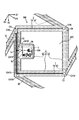
- FIG. 1 is a schematic plan view of a flexible substrate 100 according to the first embodiment.
- FIG. 2 is a schematic plan view in which a part of the flexible substrate 100 is enlarged.
- FIG. 3 is a schematic cross-sectional view of a part of the flexible substrate 100 indicated by F3A-F3B in FIG.
- FIG. 4 is a schematic cross-sectional view of a part of the flexible substrate 100 indicated by F4A-F4B in FIG.
- FIG. 5 is a schematic cross-sectional view showing the manufacturing process of the flexible substrate 100.
- FIG. 6 is a schematic cross-sectional view showing the manufacturing process subsequent to FIG.
- FIG. 7 is a schematic cross-sectional view showing the manufacturing process subsequent to FIG.
- FIG. 8 is a schematic cross-sectional view showing the manufacturing process subsequent to FIG.
- FIG. 9 is a schematic cross-sectional view showing the manufacturing process subsequent to FIG.
- FIG. 10 is a schematic plan view of the flexible substrate 200 according to the second embodiment.
- FIG. 11 is an enlarged schematic plan view of the flexible substrate 200.
- FIG. 12 is a schematic plan view of a flexible substrate 300 according to the third embodiment.
- FIG. 13 is a cross-sectional view schematically showing a connection mode of scanning lines and signal lines and electrical elements in the flexible substrate 300.
- FIG. 14 is a schematic cross-sectional view of the flexible substrate 300 in the vicinity of the corner C9 of FIG.
- FIG. 15 is a schematic cross-sectional view of the flexible substrate 300 in the vicinity of the corner C7 of FIG.
- FIG. 16 is a schematic cross-sectional view of the flexible substrate 300 in the vicinity of the corner C8 of FIG.
- FIG. 17 is a schematic cross-sectional view of the flexible substrate 300 in the vicinity of the corner C10 of FIG.
- FIG. 1 is a schematic plan view of a flexible substrate 100 according to the first embodiment.
- a first direction D1, a second direction D2, a third direction D3, and a fourth direction D4 are defined as illustrated.
- Each of the directions D1 to D4 is parallel to the main surface of the flexible substrate 100 and intersects each other.
- the first direction D1 and the second direction D2 intersect perpendicularly in the present embodiment, but may intersect at an angle other than perpendicular.
- the third direction D3 and the fourth direction D4 intersect perpendicularly in the present embodiment, but may intersect at an angle other than perpendicular.
- the flexible substrate 100 includes a plurality of scanning lines 1, a plurality of signal lines 2, and a plurality of electrical elements 3.
- the scanning line 1 and the signal line 2 are examples of wirings provided in the flexible substrate 100.
- the scanning line 1 and the signal line 2 can be formed of, for example, a metal material or a transparent conductive material, and may have a single layer structure or a laminated structure.
- the flexible substrate 100 may include other types of wiring such as a power supply line that supplies power to the electrical element 3.
- the plurality of scanning lines 1 generally extend in the first direction D1 and are aligned in the second direction D2.
- the plurality of signal lines 2 extend in the second direction D2 as a whole and are arranged in the first direction D1.
- the scanning line 1 has a wave shape in which a straight line portion parallel to the first direction D1, a straight line portion parallel to the third direction D3, and a straight line portion parallel to the second direction D2 are sequentially repeated.
- the signal line S has a wave shape in which a straight line portion parallel to the second direction D2, a straight line portion parallel to the fourth direction D4, and a straight line portion parallel to the first direction D1 are sequentially repeated.
- a polygonal region A is formed by two adjacent scanning lines 1 and two adjacent signal lines 2.
- the region A having the same shape is repeated in the first direction D1 and the second direction D2.
- the electrical element 3 is electrically connected to the scanning line 1 and the signal line 2.
- the electrical element 3 is disposed in a portion where the scanning line 1 and the signal line 2 are parallel to the second direction D2.
- the arrangement position of the electrical element 3 is not limited to this example.
- the electrical element 3 is a sensor, a semiconductor element, or an actuator.
- a temperature sensor, a pressure sensor, a touch sensor, or the like can be applied as the sensor.
- a light-emitting element, a light-receiving element, a diode, a transistor, or the like can be applied as a semiconductor element.
- the electrical element 3 is a light emitting element, a flexible display having flexibility and stretchability can be realized.
- the light emitting element for example, a light emitting diode or an organic electroluminescence element can be applied.
- the electrical element 3 is not limited to those exemplified here, and other elements having various functions can be applied.
- the electrical element 3 may be a capacitor or a resistor.
- the scanning line 1 supplies a scanning signal to the electrical element 3.
- the electrical element 3 is accompanied by output of a signal such as a sensor, the output signal from the electrical element 3 is supplied to the signal line 2.
- a drive signal is supplied to the signal line 2.
- a controller including a scan signal supply source, a drive signal supply source, or a processor that processes an output signal may be provided in the flexible substrate 100 or may be provided in a device connected to the flexible substrate 100.
- FIG. 2 is a schematic plan view in which a part of the flexible substrate 100 is enlarged.
- the scanning line 1 and the signal line 2 are close to each other and extend in parallel.
- the scanning line 1 and the signal line 2 are close to each other and extend in parallel.
- the flexible substrate 100 includes a flexible insulating base 4 that supports the scanning lines 1 and the signal lines 2.
- the insulating base material 4 can be formed of, for example, polyimide, but is not limited to this example.
- the insulating substrate 4 includes a plurality of line portions 41, a plurality of line portions 42 (dummy line portions), and a plurality of island-shaped portions 43.
- the line portion 41 overlaps at least one of the scanning line 1 and the signal line 2.
- the line part 42 does not overlap with either the scanning line 1 or the signal line 2.
- the line part 41 and the line part 42 are both linear.
- the island portion 43 overlaps with the electrical element 3 and is connected to the line portion 41.
- the line part 42 is an example of a first line part.
- the line part 41 is an example of a second line part.
- the polygonal first opening AP1 and the polygonal second opening AP2 different from the first opening AP2 are formed by the line part 41 and the line part 42.
- the first opening AP1 is a star-shaped octagon having eight corners C1 to C8.
- the second opening AP2 is a rectangle having four corners C7 to C10.
- the corner portions C1 to C10 are portions where two or more line portions 41 or the line portions 41 and the line portions 42 are connected at different angles.
- the shapes of the first opening AP1 and the second opening AP2 are not limited to these examples, and various shapes can be adopted.
- a plurality of line portions 41 and 42 (first plurality of line portions) connected to the line portion 42 between the first opening AP1 and the second opening AP2 to form the first opening AP1.
- the number of the plurality of line portions 41 and 42 (second plurality of line portions) connected to the line portion 42 between the first opening AP1 and the second opening AP2 to form the second opening AP2 are different.
- the number of the line parts 41 and 42 which comprise 1st opening AP1 and the number of the line parts 41 and 42 which comprise 2nd opening AP2 may be the same.
- the line part 41 between the corner part C1 and the corner part C2 and the line part 41 between the corner part C7 and the corner part C10 overlap with the scanning line 1 and are parallel to the first direction D1.
- the line part 41 between the corner part C5 and the corner part C6 and the line part 41 between the corner part C8 and the corner part C9 overlap with the signal line 2 and are parallel to the first direction D1.
- the line part 41 between the corner part C3 and the corner part C4 and the line part 41 between the corner part C9 and the corner part C10 overlap with the scanning line 1 and the signal line 2, and are parallel to the second direction D2. It is.
- the line part 42 between the corner part C7 and the corner part C8 does not overlap with either the scanning line 1 or the signal line 2, and is parallel to the second direction D2.
- the first opening AP1 and the second opening AP2 are constituted by a plurality of line portions 41 and 42 that respectively extend in four different directions.
- the first opening AP1 and the second opening AP2 are included in one region A.
- the first opening AP1 and the second opening AP2 correspond to two regions obtained by dividing the region A by the line portion 42.
- the line portion 42 is disposed at the boundary between the first opening AP1 and the second opening AP2.
- the inner angle ⁇ 1 of the first opening AP1 at the corners C1, C3, C5, C7 is smaller than the inner angle ⁇ 2 of the first opening AP1 at the corners C2, C4, C6, C8 ( ⁇ 1 ⁇ 2).
- the internal angle ⁇ 1 is an acute angle ( ⁇ 1 ⁇ 90 °)
- the internal angle ⁇ 2 is an angle exceeding 180 ° ( ⁇ 2> 180 °).
- the shape of the first opening AP1 is a four-fold symmetry that becomes the same shape when rotated 90 °.
- the first opening AP1 may have four or more rotational symmetries such as a five-fold symmetry and a six-fold symmetry.
- the first opening AP1 may have a symmetry of 3 times or less.
- the island portion 43 is disposed near the center of the line portion 41 that overlaps the scanning line 1 and the signal line 2.
- the electrical element 3 is disposed above the island-shaped portion 43.
- the island portion 43 is larger than the electrical element 3, and the island portion 43 protrudes from the edge of the electrical element 3 in FIG. 2.
- the length L1 from the upper end portion of the line portion 41 in the drawing to the island-like portion 43, and the lower end portion in the drawing to the island-like portion.
- the lengths L2 up to 43 are equal to each other. However, the length L1 and the length L2 may be different.
- the scanning line 1 has a first portion 11 indicated by a solid line and a second portion 12 indicated by a broken line.
- the second portion 12 overlaps with the electrical element 3.
- the first portion 11 and the second portion 12 are arranged in different layers and are electrically connected through contact holes CH1 and CH2.
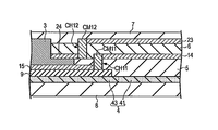
- FIG. 3 is a schematic cross-sectional view of a part of the flexible substrate 100 indicated by F3A-F3B in FIG.
- the flexible substrate 100 further includes a first organic insulating layer 5, a second organic insulating layer 6, a coating layer 7, and a support film 8 in addition to the above-described elements.
- Both the first organic insulating layer 5 and the second organic insulating layer 6 are formed of an organic material.
- the coating layer 7 is made of, for example, parylene (polyparaxylylene).
- the first organic insulating layer 5 covers the upper surface of the insulating base material 4.
- the scanning line 1 (first portion 11) is disposed on the first organic insulating layer 5.
- the second organic insulating layer 6 covers the scanning line 1 and the first organic insulating layer 5.
- the signal line 2 is disposed on the second organic insulating layer 6.
- the coating layer 7 covers the signal line 2, the insulating base 4, the first organic insulating layer 5, and the second organic insulating layer 6.
- the support film 8 covers the lower surface of the insulating base material 4. In the region where the insulating base 4 is not present, the coating layer 7 and the support film 8 are in contact with each other. That is, the support film 8 overlaps the plurality of line portions 41 and 42, the first opening AP1, and the second opening AP2 in plan view.
- the support film 8 may be formed by applying a resin material to the lower surfaces of the insulating substrate 4 and the coating layer 7 or may be attached via an adhesive layer.
- the 1st organic insulating layer 5 and the 2nd organic insulating layer 6 may be provided also in the area
- an arrangement mode as shown in FIG. 3 is preferable.
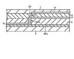
- FIG. 4 is a schematic cross-sectional view of a part of the flexible substrate 100 indicated by F4A-F4B in FIG.
- An inorganic insulating layer 9 (passivation layer) is formed between the electrical element 3 and the island portion 43.
- the inorganic insulating layer 9 has an island shape overlapping the electrical element 3 in plan view.
- the first portion 11 of the scanning line 1 is disposed on the first organic insulating layer 5.
- the second portion 12 of the scanning line 1 is disposed on the inorganic insulating layer 9 (that is, below the first organic insulating layer 5).
- the second portion 12 is electrically connected to the electrical element 3.
- the end portion of the second portion 12 is covered with the first organic insulating layer 5.
- the contact holes CH1 and CH2 described above are provided in the first organic insulating layer 5 in a region overlapping with the island-shaped portion 43 and the inorganic insulating layer 9 in plan view.
- the first portion 11 of the scanning line 1 is electrically connected via connection members CM1 and CM2 disposed in the contact holes CH1 and CH2, respectively.
- the connection members CM ⁇ b> 1 and CM ⁇ b> 2 may be part of the first portion 11, or may be provided separately from the first portion 11.
- FIG. 5 to 9 are schematic cross-sectional views sequentially showing an example of a method for manufacturing the flexible substrate 100.
- the insulating base material 4 is formed on the glass substrate GL.
- the insulating base 4 has convex portions corresponding to the line portions 41, the line portions 42, and the island-shaped portions 43.
- the insulating base material 4 is also formed in regions corresponding to the first opening AP1 and the second opening AP2.
- a scanning line 1, a signal line 2, an electrical element 3, a first organic insulating layer 5, a second organic insulating layer 6, and an inorganic insulating layer 9 are formed above the line portion 41, the line portion 42, and the island-shaped portion 43. Has been.
- the thickness T1 of the insulating base material 4 in the region corresponding to the first opening AP1 and the second opening AP2 is 1 ⁇ m or more and 2 ⁇ m or less (1 ⁇ m ⁇ T1 ⁇ 2 ⁇ m).
- the thickness T2 of the insulating substrate 4 in the region corresponding to the line portion 41, the line portion 42, and the island-shaped portion 43 is not less than T1 and not more than 20 ⁇ m (T1 ⁇ T2 ⁇ 20 ⁇ m).
- a coating layer 7 is formed.
- the coating layer 7 fills a region corresponding to the first opening AP1 and the second opening AP2, and is continuous throughout the flexible substrate 100 through the line 41, the line 42, and the island 43.
- the temporary support film TF is stuck on the upper surface of the coating layer 7.
- a polyethylene terephthalate (PET) film can be used as the temporary support film TF.
- PET polyethylene terephthalate
- the laser beam LZ is irradiated from below the glass substrate GL, and the glass substrate GL and the insulating base material 4 are peeled off.
- a support film 8 is formed on the lower surfaces of the insulating base 4 and the coating layer 7.
- the support film 8 may be formed by applying a resin material to the lower surfaces of the insulating base material 4 and the coating layer 7, or a support film 8 prepared in advance may be attached via an adhesive layer. Thereafter, the temporary support film TF is peeled to obtain the flexible substrate 100 having the cross-sectional shape shown in FIGS. 3 and 4.
- the insulating base material 4 has the first opening AP1 and the second opening AP2.
- the flexible substrate 100 can be provided with stretchability and flexibility in various directions.
- the line part 41 and the line part 42 which comprise 1st opening AP1 and 2nd opening AP2 are linear form used as the basis of general array design. Therefore, compared to the case where a curved pattern such as a meander shape is used, it is extremely easy to narrow the scanning lines 1 and the signal lines 2 and increase the density of the electrical elements 3.
- the line part 42 does not overlap with either the scanning line 1 or the signal line 2. As described above, by providing the line portion 42 that does not support the wiring, it is possible to realize a preferable shape of the first opening AP1 and the second opening AP2 regardless of the shape of the scanning line 1 and the signal line 2.
- the first opening AP1 and the second opening AP2 are included in a region A defined by two adjacent scanning lines 1 and two adjacent signal lines 2. Since the area A is arranged in a matrix on the entire flexible substrate 100, the first openings AP1 and the second openings AP2 are also distributed and arranged on the entire flexible substrate 100. Thereby, good stretchability and flexibility can be imparted to a wide range of the flexible substrate 100.
- the first opening AP1 has a four-fold symmetrical shape. Therefore, compared with the case where 1st opening AP1 is a 2 times symmetrical shape, for example, the stretchability of the flexible substrate 100 and the direction dependence degree of flexibility can be reduced.
- the first opening AP1 includes an internal angle ⁇ 2 of 180 ° or more. If the shape includes such a large inner angle, the area of the first opening AP1 can be reduced as compared with the case where the first opening AP1 is formed only with an inner angle of less than 180 °. As a result, the scanning lines 1, the signal lines 2, and the electrical elements 3 can be formed with high density.
- an island-shaped inorganic insulating layer 9 is disposed between the electrical element 3 and the insulating base 4. Since the inorganic element 9 protects the electrical element 3 and the second portion 12 of the scanning line 1, the reliability of the flexible substrate 100 can be improved. On the other hand, since an inorganic film is more susceptible to cracking than an organic film, when a wiring is formed on the inorganic film, disconnection associated with the crack may occur. However, in FIG. 4, the inorganic insulating layer 9 is not provided below the first portion 11 of the scanning line 1 or the signal line 2. Therefore, disconnection of the scanning line 1 and the signal line 2 is difficult to occur.
- the inorganic insulating layer 9 is provided on the entire flexible substrate 100, the stretchability and flexibility of the flexible substrate 100 may be hindered. However, if the inorganic insulating layer 9 is formed in an island shape, this is the case. No problems arise.
- the degree of design freedom in the vicinity of the electrical element 3 is improved.
- these contact holes CH1 and CH2 are provided above the inorganic insulating layer 9, the reliability at the connection position of the first portion 11 and the second portion 12 is also increased.
- an island-shaped portion 43 of the insulating base material 4 is disposed below the electrical element 3, below the electrical element 3, an island-shaped portion 43 of the insulating base material 4 is disposed below the electrical element 3, an island-shaped portion 43 of the insulating base material 4 is disposed below the electrical element 3, an island-shaped portion 43 of the insulating base material 4 is disposed below the electrical element 3, an island-shaped portion 43 of the insulating base material 4 is disposed below the electrical element 3 can be favorably supported. Furthermore, the insulating base material 4 is supported by the support film 8, and this support film 8 overlaps not only the line part 41, the line part 42, and the island part 43 but also the first opening AP1 and the second opening AP2. Yes. Providing such a support film 8 increases the strength of the flexible substrate 100 as a whole, and also prevents moisture from entering from below, so that reliability is also improved.
- the electrical element 3 is disposed on the line portion 41 and is located away from the connection point between the line portions 41. Thereby, even when the flexible substrate 100 is expanded or contracted or bent, the stress is not easily transmitted to the vicinity of the electrical element 3. Therefore, the reliability of the electrical element 3 is improved. As described above, if the lengths L1 and L2 from both ends of the line portion 41 to the island-shaped portion 43 are equal, the stress applied to the electrical element 3 can be reduced extremely well. In addition to the above, various suitable effects can be obtained from this embodiment.
- FIG. 10 is a schematic plan view of the flexible substrate 200 according to this embodiment.
- a fifth direction D5 and a sixth direction D6 are defined as illustrated.
- Each of the directions D1 to D6 is parallel to the main surface of the flexible substrate 200 and intersects each other.
- the scanning line 1 has a wave shape in which a straight line portion parallel to the first direction D1, a straight line portion parallel to the third direction D3, a straight line portion parallel to the first direction D1, and a straight line portion parallel to the fifth direction D5 are sequentially repeated. It has a shape.
- the signal line 2 has a wave shape in which a straight line portion parallel to the second direction D2, a straight line portion parallel to the fourth direction D4, a straight line portion parallel to the second direction D2, and a straight line portion parallel to the sixth direction D6 are sequentially repeated. It has a shape.
- a polygonal first region A1 and a second region A2 are formed by two adjacent scanning lines 1 and two adjacent signal lines 2.
- the first region A1 and the second region A2 are alternately repeated in the first direction D1 in the row between the two adjacent scanning lines 1.
- the shapes of the first region A1 and the second region A2 are line symmetric with respect to an axis parallel to the first direction D1.
- the first region A1 and the second region A2 are alternately repeated in the second direction D2 in the column between the two adjacent signal lines 2. Further, in the rows CL1 and CL2 shown in the drawing, the shapes of the first region A1 and the second region A2 are line symmetric with respect to an axis parallel to the second direction D2.
- the scanning line 1 has an extended portion 13.
- the extending portion 13 extends toward the electrical element 3 from a position where the scanning line 1 is bent. Except for the extended portion 13, the scanning line 1 and the signal line 2 do not run in parallel. Thereby, capacitive coupling between the scanning line 1 and the signal line 2 can be suppressed. Further, except for the extended portion 13, the scanning line 1 and the signal line 2 are bent at an obtuse angle. Thereby, compared with the case where it bends at an acute angle, the stress concentration to a bending part can be suppressed.
- FIG. 11 is a schematic plan view in which the row RW1 of the flexible substrate 200 is enlarged. Although the extended portion 13 of the scanning line 1 and the signal line 2 extend close to each other in the vicinity of the electrical element 3, the extended portion 13 and the signal line 2 are actually connected to the flexible substrate. 200 are stacked in the thickness direction.
- the scanning line 1 and the signal line 2 are overlapped with the line part 41.
- a plurality of line portions 42 are arranged in the first region A1.
- the line part 42 is not arrange
- the line portion 41 and the line portion 42 form a polygonal first opening AP1 and two second openings AP2.
- a polygonal third opening AP3 is formed by the line portion 41.
- the first opening AP1 is an octagon having eight corners C11 to C18.
- the second opening AP2 is the same rectangle as the second opening AP2 shown in FIG.
- the third opening AP3 is the same star-shaped octagon as the first opening AP1 shown in FIG.
- the line part 42 between the corner part C11 and the corner part C12 and the line part 42 between the corner part C15 and the corner part C16 are parallel to the first direction D1.
- the line part 42 between the corner part C12 and the corner part C13 and the line part 42 between the corner part C16 and the corner part C17 are parallel to the second direction D2.
- the line part 41 between the corner part C13 and the corner part C14 and the line part 41 between the corner part C17 and the corner part C18 overlap with the scanning line 1 and are parallel to the fifth direction D5.
- the line part 41 between the corner part C14 and the corner part C15 and the line part 41 between the corner part C11 and the corner part C18 overlap with the signal line 2 and are parallel to the fourth direction D4.
- the first area A1 includes the first opening AP1 and the two second openings AP2, and the second area A2 includes the third opening AP3.
- the shapes of the openings AP1 to AP3 in the row RW2 are symmetrical with respect to the openings AP1 to AP3 in the row RW1 with respect to an axis parallel to the first direction D1.
- the first opening AP1 of the row RW2 includes a line portion 41 parallel to the third direction D3 and a line portion 41 parallel to the sixth direction D6.
- the pattern of the insulating base material 4 is configured by a plurality of line portions 41 and 42 that extend in six different directions.
- the inner angle ⁇ 3 of the first opening AP1 at the corners C11, C13, C15, C17 is an acute angle ( ⁇ 3 ⁇ 90 °).
- the internal angle ⁇ 4 of the first opening AP1 at the corners C12 and C16 is an angle of 180 ° or more ( ⁇ 4> 180 °), and is 270 ° in one example.
- the internal angle ⁇ 5 of the first opening AP1 at the corners C14 and C18 is an angle of 180 ° or more and ⁇ 4 or less (180 ° ⁇ 5 ⁇ 4).
- the first opening AP1 is two-fold symmetric and has the same shape when rotated 180 °. Without being limited to this example, the first opening AP1 may have three or more rotational symmetry.
- the extended portion 13 of the scanning line 1 is overlapped with the line portion 41 on which the electrical element 3 is arranged.
- the extended portion 13 is formed in the same layer as the first portion 11 and is electrically connected to the second portion 12 below the electrical element 3 through the contact hole CH.
- the contact hole CH penetrates the organic insulating layer 5 similarly to the contact holes CH1 and CH2 in the first embodiment, and overlaps with the inorganic insulating layer 9 and the island-shaped portion 43 in plan view.
- the insulating base 4 has three types of openings AP1 to AP3 having different shapes.
- the flexible substrate 100 can be provided with stretchability and flexibility in multiple directions as compared to the first embodiment.
- the first opening AP1 and the two second openings AP2 are included in the first area A1, and the third opening AP3 is included in the second area A2.
- the first region A1 and the second region A2 are alternately repeated in both the first direction D1 and the second direction D2.
- the openings AP1 to AP3 are arranged in a dispersed manner, and good stretchability and flexibility can be imparted to a wide range of the flexible substrate 200.
- the shapes of the openings AP1 to AP3 are inverted for each row or column, and there are a plurality of line portions 41 and 42 extending in six different directions, the elasticity of the flexible substrate 100 and The direction dependency of flexibility can be reduced extremely well.
- FIG. 12 is a schematic plan view of the flexible substrate 300 according to the present embodiment.
- the planar shapes of the scanning line 1, the signal line 2, and the insulating base 4 are the same as those in FIG. 2, and in FIG. 12, the second opening AP2 having corners C7 to C10 and the vicinity thereof are enlarged.
- the first portion 11 of the scanning line 1 is disposed between the corner C9 and the corner C10 and between the corner C10 and the corner C7.
- the other part of the scanning line 1 that overlaps with the line part 41 is a second part 12 arranged in a different layer from the first part 11.
- the electrical element 3 is disposed inside the second opening AP2 in the vicinity of the line portion 41 between the corner portion C9 and the corner portion C10.
- the island-shaped portion 43 protrudes from the line portion 41 to the inside of the second opening AP2.
- the signal line 2 has a first portion 21 indicated by a solid line and a second portion 22 indicated by a broken line.
- the first portion 21 and the second portion 22 are arranged in different layers.
- the 1st part 21 is arrange
- the other part of the signal line 2 overlapping the line part 41 is the second part 22.
- the scanning line 1 has a first extension portion 14 and a second extension portion 15 in the vicinity of the electrical element 3. These extending portions 14 and 15 are electrically connected through the contact hole CH11.
- the first extending portion 14 is disposed in the same layer as the first portion 11, and the second extending portion 15 is disposed in the same layer as the second portion 12.
- the signal line 2 has a first extension portion 23 and a second extension portion 24 in the vicinity of the electrical element 3. These extending portions 23 and 24 are electrically connected through the contact hole CH12.
- the first extending portion 23 is disposed in the same layer as the first portion 21, and the second extending portion 24 is disposed in the same layer as the second portion 22.
- the second extending portion 15 of the scanning line 1 is connected to the gate of the switching element SW included in the electrical element 3.
- the second extending portion 24 of the signal line 2 is connected to the source or drain of the switching element SW.
- the first portion 11 and the second portion 12 of the scanning line 1 are electrically connected through the contact hole CH13.
- the first portion 11 and the second portion 12 of the scanning line 1 are electrically connected through the contact hole CH14.
- the first portion 21 and the second portion 22 of the signal line 2 are electrically connected through the contact hole CH15.
- the first portion 21 and the second portion 22 of the signal line 2 are electrically connected through the contact hole CH16.
- FIG. 13 is a cross-sectional view schematically showing a connection mode between the scanning line 1 and the signal line 2 and the electrical element 3.
- the extended portions 14 and 15 of the scanning line 1 and the contact hole CH11, and the extended portions 23 and 24 of the signal line 2 and the contact hole CH12 are shown in the same cross section.
- the contact hole CH11 is provided in the first organic insulating layer 5.
- the contact hole CH12 is provided in the second organic insulating layer 6.
- the contact holes CH11 and CH12 overlap with the island-shaped portion 43 and the inorganic insulating layer 9 in plan view.
- the first extension portion 14 and the second extension portion 15 of the scanning line 1 are electrically connected via a connection member CM11 disposed in the contact hole CH11.
- the first extension portion 23 and the second extension portion 24 of the signal line 2 are electrically connected via a connection member CM12 disposed in the contact hole CH12.
- the connection member CM11 may be a part of the first extension portion 14, or may be provided separately from the first extension portion 14.
- the connection member CM12 may be a part of the first extension portion 23, or may be provided separately from the first extension portion 23.
- FIG. 14 is a schematic cross-sectional view of the flexible substrate 300 along the scanning line 1 in the vicinity of the corner C9.
- the first portion 11 of the scanning line 1 is disposed on the first organic insulating layer 5.
- the second portion 12 of the scanning line 1 is disposed on the insulating substrate 4 (line portion 41).
- the contact hole CH13 is provided in the first organic insulating layer 5.
- the first portion 11 and the second portion 12 are electrically connected via a connection member CM13 disposed in the contact hole CH13.
- FIG. 15 is a schematic cross-sectional view of the flexible substrate 300 along the scanning line 1 in the vicinity of the corner C7.
- the contact hole CH14 is provided in the first organic insulating layer 5.
- the first portion 11 and the second portion 12 of the scanning line 1 are electrically connected via a connection member CM14 disposed in the contact hole CH14.
- FIG. 16 is a schematic cross-sectional view of the flexible substrate 300 along the signal line 2 in the vicinity of the corner C8.
- the first portion 21 of the signal line 2 is disposed on the second organic insulating layer 6.
- the second portion 22 of the signal line 2 is disposed on the insulating substrate 4 (line portion 41).
- the contact hole CH15 is provided in the first organic insulating layer 5 and the second organic insulating layer 6.
- the first portion 21 and the second portion 22 are electrically connected via a connection member CM15 disposed in the contact hole CH15.
- FIG. 17 is a schematic cross-sectional view of the flexible substrate 300 along the signal line 2 in the vicinity of the corner C10.
- the contact hole CH ⁇ b> 16 is provided in the first organic insulating layer 5 and the second organic insulating layer 6.
- the first portion 21 and the second portion 22 of the signal line 2 are electrically connected via a connection member CM16 disposed in the contact hole CH16.
- connection members CM11, CM13, and CM14 may be part of the first portion 11 of the scanning line 1 or may be provided separately from the first portion 11. Further, the connection members CM12, CM15, and CM16 may be a part of the first portion 21 of the signal line 2 or may be provided separately from the first portion 21.
- the flexible substrate 300 When the flexible substrate 300 is stretched or bent, a large stress is applied to the position where the two line portions of the insulating base 4 are connected, that is, the bent portions of the scanning line 1 and the signal line 2.
- the scanning line 1 is divided into the first portion 11 and the second portion 12 and connected through the contact hole at the bent portion as in this embodiment, the stress applied to the scanning line 1 at the bent portion can be relaxed.
- the signal line 2 is divided into the first part 21 and the second part 22 and is connected through the contact hole at the bent part, the stress applied to the signal line 2 at the bent part can be relieved. Accordingly, disconnection of the scanning line 1 and the signal line 2 can be suppressed.
- the shape of the opening of the insulating base material 4 and the shape of the region formed by the scanning lines 1 and the signal lines 2 are not limited to those disclosed in the first to third embodiments.
- the insulating base material 4 may not have the line portion 42 that does not overlap with either the scanning line 1 or the signal line 2.
- the insulating base material 4 may include a curved line part in at least a part in addition to the linear line part.
Landscapes
- Engineering & Computer Science (AREA)
- Microelectronics & Electronic Packaging (AREA)
- Physics & Mathematics (AREA)
- General Physics & Mathematics (AREA)
- Theoretical Computer Science (AREA)
- Structure Of Printed Boards (AREA)
- Devices For Indicating Variable Information By Combining Individual Elements (AREA)
Priority Applications (2)
| Application Number | Priority Date | Filing Date | Title |
|---|---|---|---|
| CN201980021944.8A CN111903197B (zh) | 2018-03-27 | 2019-01-24 | 柔性基板 |
| US17/032,228 US11557739B2 (en) | 2018-03-27 | 2020-09-25 | Flexible substrate |
Applications Claiming Priority (2)
| Application Number | Priority Date | Filing Date | Title |
|---|---|---|---|
| JP2018060196A JP7134665B2 (ja) | 2018-03-27 | 2018-03-27 | フレキシブル基板 |
| JP2018-060196 | 2018-03-27 |
Related Child Applications (1)
| Application Number | Title | Priority Date | Filing Date |
|---|---|---|---|
| US17/032,228 Continuation US11557739B2 (en) | 2018-03-27 | 2020-09-25 | Flexible substrate |
Publications (1)
| Publication Number | Publication Date |
|---|---|
| WO2019187568A1 true WO2019187568A1 (ja) | 2019-10-03 |
Family
ID=68058723
Family Applications (1)
| Application Number | Title | Priority Date | Filing Date |
|---|---|---|---|
| PCT/JP2019/002357 Ceased WO2019187568A1 (ja) | 2018-03-27 | 2019-01-24 | フレキシブル基板 |
Country Status (4)
| Country | Link |
|---|---|
| US (1) | US11557739B2 (https=) |
| JP (1) | JP7134665B2 (https=) |
| CN (1) | CN111903197B (https=) |
| WO (1) | WO2019187568A1 (https=) |
Cited By (3)
| Publication number | Priority date | Publication date | Assignee | Title |
|---|---|---|---|---|
| JP2021150584A (ja) * | 2020-03-23 | 2021-09-27 | 株式会社ジャパンディスプレイ | 電子機器 |
| WO2021192505A1 (ja) * | 2020-03-23 | 2021-09-30 | 株式会社ジャパンディスプレイ | 電子機器 |
| US20220278046A1 (en) * | 2019-11-28 | 2022-09-01 | Japan Display Inc. | Flexible substrate |
Families Citing this family (5)
| Publication number | Priority date | Publication date | Assignee | Title |
|---|---|---|---|---|
| JP2021097097A (ja) * | 2019-12-16 | 2021-06-24 | 株式会社ジャパンディスプレイ | フレキシブル基板 |
| JP7500192B2 (ja) * | 2019-12-26 | 2024-06-17 | 株式会社ジャパンディスプレイ | フレキシブル基板及び電子機器 |
| JP7551303B2 (ja) * | 2020-03-02 | 2024-09-17 | 株式会社ジャパンディスプレイ | 電子機器 |
| KR102628302B1 (ko) * | 2021-08-02 | 2024-01-23 | 고려대학교 산학협력단 | 신축/유연 마이크로 발광다이오드 제조 방법 |
| JP7837542B2 (ja) * | 2022-04-06 | 2026-03-31 | 株式会社Magnolia White | フレキシブル基板 |
Citations (4)
| Publication number | Priority date | Publication date | Assignee | Title |
|---|---|---|---|---|
| JP2008089633A (ja) * | 2006-09-29 | 2008-04-17 | Seiko Epson Corp | 電気光学装置及び電子機器 |
| US20100330338A1 (en) * | 2009-06-29 | 2010-12-30 | Boyce Mary C | Structured material substrates for flexible, stretchable electronics |
| JP2015198102A (ja) * | 2014-03-31 | 2015-11-09 | パナソニックIpマネジメント株式会社 | 伸縮性フレキシブル基板およびその製造方法 |
| US20170057704A1 (en) * | 2015-08-26 | 2017-03-02 | The University Of New Hampshire | Chiral Structures With Adjustable Auxetic Effects |
Family Cites Families (7)
| Publication number | Priority date | Publication date | Assignee | Title |
|---|---|---|---|---|
| JP6191991B2 (ja) * | 2014-03-31 | 2017-09-06 | パナソニックIpマネジメント株式会社 | 伸縮性フレキシブル基板およびその製造方法 |
| JP6300156B2 (ja) | 2014-03-31 | 2018-03-28 | パナソニックIpマネジメント株式会社 | 伸縮性フレキシブル基板およびその製造方法 |
| KR102363908B1 (ko) * | 2014-10-08 | 2022-02-17 | 삼성디스플레이 주식회사 | 신장 가능 필름, 이의 제조방법 및 이를 포함하는 표시 장치 |
| US20170181276A1 (en) | 2015-12-21 | 2017-06-22 | Panasonic Intellectual Property Management Co., Ltd. | Substrate including stretchable sheet |
| JP6756508B2 (ja) * | 2016-04-04 | 2020-09-16 | 株式会社ジャパンディスプレイ | 表示装置 |
| US10199323B2 (en) * | 2016-08-30 | 2019-02-05 | Apple Inc. | Flexible circuit substrate with temporary supports and equalized lateral expansion |
| JP2020088331A (ja) * | 2018-11-30 | 2020-06-04 | 株式会社ジャパンディスプレイ | フレキシブル基板 |
-
2018
- 2018-03-27 JP JP2018060196A patent/JP7134665B2/ja active Active
-
2019
- 2019-01-24 WO PCT/JP2019/002357 patent/WO2019187568A1/ja not_active Ceased
- 2019-01-24 CN CN201980021944.8A patent/CN111903197B/zh active Active
-
2020
- 2020-09-25 US US17/032,228 patent/US11557739B2/en active Active
Patent Citations (4)
| Publication number | Priority date | Publication date | Assignee | Title |
|---|---|---|---|---|
| JP2008089633A (ja) * | 2006-09-29 | 2008-04-17 | Seiko Epson Corp | 電気光学装置及び電子機器 |
| US20100330338A1 (en) * | 2009-06-29 | 2010-12-30 | Boyce Mary C | Structured material substrates for flexible, stretchable electronics |
| JP2015198102A (ja) * | 2014-03-31 | 2015-11-09 | パナソニックIpマネジメント株式会社 | 伸縮性フレキシブル基板およびその製造方法 |
| US20170057704A1 (en) * | 2015-08-26 | 2017-03-02 | The University Of New Hampshire | Chiral Structures With Adjustable Auxetic Effects |
Cited By (7)
| Publication number | Priority date | Publication date | Assignee | Title |
|---|---|---|---|---|
| US20220278046A1 (en) * | 2019-11-28 | 2022-09-01 | Japan Display Inc. | Flexible substrate |
| US12237270B2 (en) * | 2019-11-28 | 2025-02-25 | Japan Display Inc. | Flexible substrate |
| JP2021150584A (ja) * | 2020-03-23 | 2021-09-27 | 株式会社ジャパンディスプレイ | 電子機器 |
| WO2021192505A1 (ja) * | 2020-03-23 | 2021-09-30 | 株式会社ジャパンディスプレイ | 電子機器 |
| WO2021192506A1 (ja) * | 2020-03-23 | 2021-09-30 | 株式会社ジャパンディスプレイ | 電子機器 |
| JP7548715B2 (ja) | 2020-03-23 | 2024-09-10 | 株式会社ジャパンディスプレイ | 電子機器 |
| US12267951B2 (en) | 2020-03-23 | 2025-04-01 | Japan Display Inc. | Electronic device |
Also Published As
| Publication number | Publication date |
|---|---|
| JP7134665B2 (ja) | 2022-09-12 |
| CN111903197B (zh) | 2024-12-17 |
| US20210013431A1 (en) | 2021-01-14 |
| CN111903197A (zh) | 2020-11-06 |
| JP2019175924A (ja) | 2019-10-10 |
| US11557739B2 (en) | 2023-01-17 |
Similar Documents
| Publication | Publication Date | Title |
|---|---|---|
| WO2019187568A1 (ja) | フレキシブル基板 | |
| CN108695367B (zh) | 显示装置 | |
| US11388816B2 (en) | Flexible substrate | |
| CN111029368B (zh) | 显示装置 | |
| US10741777B2 (en) | Stretchable display | |
| US11765821B2 (en) | Flexible substrate | |
| US12112668B2 (en) | Flexible substrate | |
| WO2020110421A1 (ja) | フレキシブル基板 | |
| US20220087010A1 (en) | Flexible substrate | |
| CN117594611A (zh) | 可拉伸显示面板及可拉伸显示装置 | |
| US12177981B2 (en) | Electronic device including lines provided on elastic base | |
| US12289842B2 (en) | Method of manufacturing flexible substrate | |
| JP2021086935A (ja) | フレキシブル基板 | |
| US12310228B2 (en) | Flexible substrate | |
| TW201808059A (zh) | 可撓式電子裝置 | |
| TWM541182U (zh) | 可撓式電子裝置 | |
| US20250151192A1 (en) | Flexible substrate | |
| TWI624201B (zh) | 可撓式電子裝置 | |
| US12593401B2 (en) | Electronic device | |
| TWI634819B (zh) | 可撓式電子裝置 | |
| WO2021124667A1 (ja) | フレキシブル基板 | |
| TWM541026U (zh) | 可撓式電子裝置 |
Legal Events
| Date | Code | Title | Description |
|---|---|---|---|
| 121 | Ep: the epo has been informed by wipo that ep was designated in this application |
Ref document number: 19777607 Country of ref document: EP Kind code of ref document: A1 |
|
| NENP | Non-entry into the national phase |
Ref country code: DE |
|
| 122 | Ep: pct application non-entry in european phase |
Ref document number: 19777607 Country of ref document: EP Kind code of ref document: A1 |