WO2019176438A1 - Dispositif optique, dispositif d'affichage d'image et dispositif d'affichage - Google Patents
Dispositif optique, dispositif d'affichage d'image et dispositif d'affichage Download PDFInfo
- Publication number
- WO2019176438A1 WO2019176438A1 PCT/JP2019/005472 JP2019005472W WO2019176438A1 WO 2019176438 A1 WO2019176438 A1 WO 2019176438A1 JP 2019005472 W JP2019005472 W JP 2019005472W WO 2019176438 A1 WO2019176438 A1 WO 2019176438A1
- Authority
- WO
- WIPO (PCT)
- Prior art keywords
- deflection member
- light
- deflection
- guide plate
- incident
- Prior art date
Links
- 230000003287 optical effect Effects 0.000 title claims abstract description 181
- 210000001747 pupil Anatomy 0.000 claims abstract description 20
- 239000013598 vector Substances 0.000 claims description 32
- 210000003128 head Anatomy 0.000 claims description 4
- 239000010410 layer Substances 0.000 description 58
- 239000000463 material Substances 0.000 description 41
- 229920005989 resin Polymers 0.000 description 31
- 239000011347 resin Substances 0.000 description 31
- 238000005259 measurement Methods 0.000 description 22
- 239000004973 liquid crystal related substance Substances 0.000 description 21
- 239000000758 substrate Substances 0.000 description 20
- -1 acrylic ester Chemical class 0.000 description 14
- 238000010586 diagram Methods 0.000 description 14
- 238000000034 method Methods 0.000 description 13
- 230000005540 biological transmission Effects 0.000 description 10
- 238000005401 electroluminescence Methods 0.000 description 10
- 230000010287 polarization Effects 0.000 description 9
- PPBRXRYQALVLMV-UHFFFAOYSA-N Styrene Chemical compound C=CC1=CC=CC=C1 PPBRXRYQALVLMV-UHFFFAOYSA-N 0.000 description 8
- 239000011521 glass Substances 0.000 description 7
- 238000012986 modification Methods 0.000 description 7
- 230000004048 modification Effects 0.000 description 7
- 239000000178 monomer Substances 0.000 description 7
- 239000002245 particle Substances 0.000 description 7
- 230000007613 environmental effect Effects 0.000 description 6
- 239000011159 matrix material Substances 0.000 description 6
- 229920003023 plastic Polymers 0.000 description 6
- 239000004925 Acrylic resin Substances 0.000 description 5
- 229920000178 Acrylic resin Polymers 0.000 description 5
- 239000004743 Polypropylene Substances 0.000 description 5
- 230000000903 blocking effect Effects 0.000 description 5
- 239000004033 plastic Substances 0.000 description 5
- 229920001155 polypropylene Polymers 0.000 description 5
- 238000002834 transmittance Methods 0.000 description 5
- 238000003384 imaging method Methods 0.000 description 4
- 239000002985 plastic film Substances 0.000 description 4
- 229920005668 polycarbonate resin Polymers 0.000 description 4
- 239000004431 polycarbonate resin Substances 0.000 description 4
- 230000001902 propagating effect Effects 0.000 description 4
- 229910006404 SnO 2 Inorganic materials 0.000 description 3
- 239000011230 binding agent Substances 0.000 description 3
- 230000015572 biosynthetic process Effects 0.000 description 3
- 150000001875 compounds Chemical class 0.000 description 3
- 229920001577 copolymer Polymers 0.000 description 3
- 238000004070 electrodeposition Methods 0.000 description 3
- 239000003822 epoxy resin Substances 0.000 description 3
- 229910052751 metal Inorganic materials 0.000 description 3
- 239000002184 metal Substances 0.000 description 3
- 238000000059 patterning Methods 0.000 description 3
- 229920003229 poly(methyl methacrylate) Polymers 0.000 description 3
- 229920000647 polyepoxide Polymers 0.000 description 3
- 239000005020 polyethylene terephthalate Substances 0.000 description 3
- 229920000139 polyethylene terephthalate Polymers 0.000 description 3
- 239000004926 polymethyl methacrylate Substances 0.000 description 3
- 239000002243 precursor Substances 0.000 description 3
- 230000001681 protective effect Effects 0.000 description 3
- 238000007789 sealing Methods 0.000 description 3
- 239000004065 semiconductor Substances 0.000 description 3
- 239000007787 solid Substances 0.000 description 3
- XLOMVQKBTHCTTD-UHFFFAOYSA-N zinc oxide Inorganic materials [Zn]=O XLOMVQKBTHCTTD-UHFFFAOYSA-N 0.000 description 3
- 239000011787 zinc oxide Substances 0.000 description 3
- KAKZBPTYRLMSJV-UHFFFAOYSA-N Butadiene Chemical compound C=CC=C KAKZBPTYRLMSJV-UHFFFAOYSA-N 0.000 description 2
- 229920002284 Cellulose triacetate Polymers 0.000 description 2
- RTZKZFJDLAIYFH-UHFFFAOYSA-N Diethyl ether Chemical compound CCOCC RTZKZFJDLAIYFH-UHFFFAOYSA-N 0.000 description 2
- 239000002033 PVDF binder Substances 0.000 description 2
- 239000004372 Polyvinyl alcohol Substances 0.000 description 2
- NNLVGZFZQQXQNW-ADJNRHBOSA-N [(2r,3r,4s,5r,6s)-4,5-diacetyloxy-3-[(2s,3r,4s,5r,6r)-3,4,5-triacetyloxy-6-(acetyloxymethyl)oxan-2-yl]oxy-6-[(2r,3r,4s,5r,6s)-4,5,6-triacetyloxy-2-(acetyloxymethyl)oxan-3-yl]oxyoxan-2-yl]methyl acetate Chemical compound O([C@@H]1O[C@@H]([C@H]([C@H](OC(C)=O)[C@H]1OC(C)=O)O[C@H]1[C@@H]([C@@H](OC(C)=O)[C@H](OC(C)=O)[C@@H](COC(C)=O)O1)OC(C)=O)COC(=O)C)[C@@H]1[C@@H](COC(C)=O)O[C@@H](OC(C)=O)[C@H](OC(C)=O)[C@H]1OC(C)=O NNLVGZFZQQXQNW-ADJNRHBOSA-N 0.000 description 2
- 239000012298 atmosphere Substances 0.000 description 2
- 229920002301 cellulose acetate Polymers 0.000 description 2
- 238000005229 chemical vapour deposition Methods 0.000 description 2
- 238000000576 coating method Methods 0.000 description 2
- 239000002131 composite material Substances 0.000 description 2
- 210000002858 crystal cell Anatomy 0.000 description 2
- 238000013461 design Methods 0.000 description 2
- 239000006185 dispersion Substances 0.000 description 2
- 238000005530 etching Methods 0.000 description 2
- 210000001508 eye Anatomy 0.000 description 2
- 239000003999 initiator Substances 0.000 description 2
- DCYOBGZUOMKFPA-UHFFFAOYSA-N iron(2+);iron(3+);octadecacyanide Chemical compound [Fe+2].[Fe+2].[Fe+2].[Fe+3].[Fe+3].[Fe+3].[Fe+3].N#[C-].N#[C-].N#[C-].N#[C-].N#[C-].N#[C-].N#[C-].N#[C-].N#[C-].N#[C-].N#[C-].N#[C-].N#[C-].N#[C-].N#[C-].N#[C-].N#[C-].N#[C-] DCYOBGZUOMKFPA-UHFFFAOYSA-N 0.000 description 2
- 238000010030 laminating Methods 0.000 description 2
- 238000002156 mixing Methods 0.000 description 2
- 238000005240 physical vapour deposition Methods 0.000 description 2
- 229920006255 plastic film Polymers 0.000 description 2
- 229920001721 polyimide Polymers 0.000 description 2
- 229920006324 polyoxymethylene Polymers 0.000 description 2
- 229920002451 polyvinyl alcohol Polymers 0.000 description 2
- 229920002981 polyvinylidene fluoride Polymers 0.000 description 2
- 239000011241 protective layer Substances 0.000 description 2
- 229960003351 prussian blue Drugs 0.000 description 2
- 239000013225 prussian blue Substances 0.000 description 2
- 238000006479 redox reaction Methods 0.000 description 2
- 229920002050 silicone resin Polymers 0.000 description 2
- 238000012360 testing method Methods 0.000 description 2
- 229920002803 thermoplastic polyurethane Polymers 0.000 description 2
- JMMZCWZIJXAGKW-UHFFFAOYSA-N 2-methylpent-2-ene Chemical compound CCC=C(C)C JMMZCWZIJXAGKW-UHFFFAOYSA-N 0.000 description 1
- 239000005294 BK7 Substances 0.000 description 1
- 239000004593 Epoxy Substances 0.000 description 1
- YCKRFDGAMUMZLT-UHFFFAOYSA-N Fluorine atom Chemical compound [F] YCKRFDGAMUMZLT-UHFFFAOYSA-N 0.000 description 1
- 108010010803 Gelatin Proteins 0.000 description 1
- 244000043261 Hevea brasiliensis Species 0.000 description 1
- CERQOIWHTDAKMF-UHFFFAOYSA-N Methacrylic acid Chemical compound CC(=C)C(O)=O CERQOIWHTDAKMF-UHFFFAOYSA-N 0.000 description 1
- 229930040373 Paraformaldehyde Natural products 0.000 description 1
- 229930182556 Polyacetal Natural products 0.000 description 1
- 239000004952 Polyamide Substances 0.000 description 1
- 239000004962 Polyamide-imide Substances 0.000 description 1
- 239000004695 Polyether sulfone Substances 0.000 description 1
- 239000004697 Polyetherimide Substances 0.000 description 1
- 239000004698 Polyethylene Substances 0.000 description 1
- 239000002202 Polyethylene glycol Substances 0.000 description 1
- 239000004642 Polyimide Substances 0.000 description 1
- 239000004721 Polyphenylene oxide Substances 0.000 description 1
- 239000004734 Polyphenylene sulfide Substances 0.000 description 1
- 239000004793 Polystyrene Substances 0.000 description 1
- VYPSYNLAJGMNEJ-UHFFFAOYSA-N Silicium dioxide Chemical compound O=[Si]=O VYPSYNLAJGMNEJ-UHFFFAOYSA-N 0.000 description 1
- BQCADISMDOOEFD-UHFFFAOYSA-N Silver Chemical compound [Ag] BQCADISMDOOEFD-UHFFFAOYSA-N 0.000 description 1
- 229920001807 Urea-formaldehyde Polymers 0.000 description 1
- XTXRWKRVRITETP-UHFFFAOYSA-N Vinyl acetate Chemical compound CC(=O)OC=C XTXRWKRVRITETP-UHFFFAOYSA-N 0.000 description 1
- BZHJMEDXRYGGRV-UHFFFAOYSA-N Vinyl chloride Chemical compound ClC=C BZHJMEDXRYGGRV-UHFFFAOYSA-N 0.000 description 1
- NIXOWILDQLNWCW-UHFFFAOYSA-N acrylic acid group Chemical group C(C=C)(=O)O NIXOWILDQLNWCW-UHFFFAOYSA-N 0.000 description 1
- 230000001154 acute effect Effects 0.000 description 1
- 239000000654 additive Substances 0.000 description 1
- 230000000996 additive effect Effects 0.000 description 1
- 239000000853 adhesive Substances 0.000 description 1
- 230000001070 adhesive effect Effects 0.000 description 1
- 239000000956 alloy Substances 0.000 description 1
- 229910045601 alloy Inorganic materials 0.000 description 1
- 230000004888 barrier function Effects 0.000 description 1
- 210000005252 bulbus oculi Anatomy 0.000 description 1
- QHIWVLPBUQWDMQ-UHFFFAOYSA-N butyl prop-2-enoate;methyl 2-methylprop-2-enoate;prop-2-enoic acid Chemical compound OC(=O)C=C.COC(=O)C(C)=C.CCCCOC(=O)C=C QHIWVLPBUQWDMQ-UHFFFAOYSA-N 0.000 description 1
- 229920002678 cellulose Polymers 0.000 description 1
- 239000012986 chain transfer agent Substances 0.000 description 1
- 239000003795 chemical substances by application Substances 0.000 description 1
- 238000004581 coalescence Methods 0.000 description 1
- 239000011248 coating agent Substances 0.000 description 1
- 229920001940 conductive polymer Polymers 0.000 description 1
- 239000000470 constituent Substances 0.000 description 1
- 238000007796 conventional method Methods 0.000 description 1
- 230000007423 decrease Effects 0.000 description 1
- 238000000151 deposition Methods 0.000 description 1
- 230000008021 deposition Effects 0.000 description 1
- 238000011161 development Methods 0.000 description 1
- 239000002612 dispersion medium Substances 0.000 description 1
- 238000010494 dissociation reaction Methods 0.000 description 1
- 230000005593 dissociations Effects 0.000 description 1
- 210000003027 ear inner Anatomy 0.000 description 1
- 239000003792 electrolyte Substances 0.000 description 1
- 239000005357 flat glass Substances 0.000 description 1
- 229910052731 fluorine Inorganic materials 0.000 description 1
- 239000011737 fluorine Substances 0.000 description 1
- 229920002313 fluoropolymer Polymers 0.000 description 1
- 239000004811 fluoropolymer Substances 0.000 description 1
- 229920000159 gelatin Polymers 0.000 description 1
- 239000008273 gelatin Substances 0.000 description 1
- 235000019322 gelatine Nutrition 0.000 description 1
- 235000011852 gelatine desserts Nutrition 0.000 description 1
- LNEPOXFFQSENCJ-UHFFFAOYSA-N haloperidol Chemical compound C1CC(O)(C=2C=CC(Cl)=CC=2)CCN1CCCC(=O)C1=CC=C(F)C=C1 LNEPOXFFQSENCJ-UHFFFAOYSA-N 0.000 description 1
- HCDGVLDPFQMKDK-UHFFFAOYSA-N hexafluoropropylene Chemical group FC(F)=C(F)C(F)(F)F HCDGVLDPFQMKDK-UHFFFAOYSA-N 0.000 description 1
- RHZWSUVWRRXEJF-UHFFFAOYSA-N indium tin Chemical compound [In].[Sn] RHZWSUVWRRXEJF-UHFFFAOYSA-N 0.000 description 1
- NJWNEWQMQCGRDO-UHFFFAOYSA-N indium zinc Chemical compound [Zn].[In] NJWNEWQMQCGRDO-UHFFFAOYSA-N 0.000 description 1
- AMGQUBHHOARCQH-UHFFFAOYSA-N indium;oxotin Chemical compound [In].[Sn]=O AMGQUBHHOARCQH-UHFFFAOYSA-N 0.000 description 1
- 239000004615 ingredient Substances 0.000 description 1
- 229910010272 inorganic material Inorganic materials 0.000 description 1
- 239000011147 inorganic material Substances 0.000 description 1
- 230000001678 irradiating effect Effects 0.000 description 1
- 239000007788 liquid Substances 0.000 description 1
- 238000004519 manufacturing process Methods 0.000 description 1
- 229910021645 metal ion Inorganic materials 0.000 description 1
- 125000005395 methacrylic acid group Chemical group 0.000 description 1
- 239000000203 mixture Substances 0.000 description 1
- 229920003052 natural elastomer Polymers 0.000 description 1
- 229920001194 natural rubber Polymers 0.000 description 1
- 239000005304 optical glass Substances 0.000 description 1
- 239000011368 organic material Substances 0.000 description 1
- 239000005011 phenolic resin Substances 0.000 description 1
- 125000000951 phenoxy group Chemical group [H]C1=C([H])C([H])=C(O*)C([H])=C1[H] 0.000 description 1
- 230000002165 photosensitisation Effects 0.000 description 1
- 239000003504 photosensitizing agent Substances 0.000 description 1
- 239000004014 plasticizer Substances 0.000 description 1
- 229920003227 poly(N-vinyl carbazole) Polymers 0.000 description 1
- 229920003207 poly(ethylene-2,6-naphthalate) Polymers 0.000 description 1
- 229920002492 poly(sulfone) Polymers 0.000 description 1
- 229920002647 polyamide Polymers 0.000 description 1
- 229920006122 polyamide resin Polymers 0.000 description 1
- 229920002312 polyamide-imide Polymers 0.000 description 1
- 229920000767 polyaniline Polymers 0.000 description 1
- 229920002857 polybutadiene Polymers 0.000 description 1
- 239000004417 polycarbonate Substances 0.000 description 1
- 229920000515 polycarbonate Polymers 0.000 description 1
- 229920000570 polyether Polymers 0.000 description 1
- 229920006393 polyether sulfone Polymers 0.000 description 1
- 229920001601 polyetherimide Polymers 0.000 description 1
- 229920000573 polyethylene Polymers 0.000 description 1
- 229920001223 polyethylene glycol Polymers 0.000 description 1
- 239000011112 polyethylene naphthalate Substances 0.000 description 1
- 239000009719 polyimide resin Substances 0.000 description 1
- 229920000642 polymer Polymers 0.000 description 1
- 239000002952 polymeric resin Substances 0.000 description 1
- 229920000069 polyphenylene sulfide Polymers 0.000 description 1
- 229920000128 polypyrrole Polymers 0.000 description 1
- 229920002223 polystyrene Polymers 0.000 description 1
- 229920005990 polystyrene resin Polymers 0.000 description 1
- 229920001343 polytetrafluoroethylene Polymers 0.000 description 1
- 239000004810 polytetrafluoroethylene Substances 0.000 description 1
- 229920000123 polythiophene Polymers 0.000 description 1
- 229920005749 polyurethane resin Polymers 0.000 description 1
- 229920002689 polyvinyl acetate Polymers 0.000 description 1
- 239000011118 polyvinyl acetate Substances 0.000 description 1
- 239000004800 polyvinyl chloride Substances 0.000 description 1
- 229920000915 polyvinyl chloride Polymers 0.000 description 1
- 229920001289 polyvinyl ether Polymers 0.000 description 1
- 230000000644 propagated effect Effects 0.000 description 1
- 230000002441 reversible effect Effects 0.000 description 1
- 229910052710 silicon Inorganic materials 0.000 description 1
- 239000010703 silicon Substances 0.000 description 1
- 229910052709 silver Inorganic materials 0.000 description 1
- 239000004332 silver Substances 0.000 description 1
- 239000005361 soda-lime glass Substances 0.000 description 1
- 239000011029 spinel Substances 0.000 description 1
- 229910052596 spinel Inorganic materials 0.000 description 1
- 238000004544 sputter deposition Methods 0.000 description 1
- 239000000126 substance Substances 0.000 description 1
- 229920003002 synthetic resin Polymers 0.000 description 1
- 210000002262 tip cell Anatomy 0.000 description 1
- 238000007740 vapor deposition Methods 0.000 description 1
- 125000000391 vinyl group Chemical group [H]C([*])=C([H])[H] 0.000 description 1
- 229920002554 vinyl polymer Polymers 0.000 description 1
- YVTHLONGBIQYBO-UHFFFAOYSA-N zinc indium(3+) oxygen(2-) Chemical compound [O--].[Zn++].[In+3] YVTHLONGBIQYBO-UHFFFAOYSA-N 0.000 description 1
- 229910000166 zirconium phosphate Inorganic materials 0.000 description 1
- LEHFSLREWWMLPU-UHFFFAOYSA-B zirconium(4+);tetraphosphate Chemical compound [Zr+4].[Zr+4].[Zr+4].[O-]P([O-])([O-])=O.[O-]P([O-])([O-])=O.[O-]P([O-])([O-])=O.[O-]P([O-])([O-])=O LEHFSLREWWMLPU-UHFFFAOYSA-B 0.000 description 1
Images


Classifications
-
- G—PHYSICS
- G02—OPTICS
- G02B—OPTICAL ELEMENTS, SYSTEMS OR APPARATUS
- G02B27/00—Optical systems or apparatus not provided for by any of the groups G02B1/00 - G02B26/00, G02B30/00
- G02B27/01—Head-up displays
- G02B27/017—Head mounted
- G02B27/0172—Head mounted characterised by optical features
-
- G—PHYSICS
- G02—OPTICS
- G02B—OPTICAL ELEMENTS, SYSTEMS OR APPARATUS
- G02B27/00—Optical systems or apparatus not provided for by any of the groups G02B1/00 - G02B26/00, G02B30/00
- G02B27/42—Diffraction optics, i.e. systems including a diffractive element being designed for providing a diffractive effect
- G02B27/4205—Diffraction optics, i.e. systems including a diffractive element being designed for providing a diffractive effect having a diffractive optical element [DOE] contributing to image formation, e.g. whereby modulation transfer function MTF or optical aberrations are relevant
-
- G—PHYSICS
- G02—OPTICS
- G02B—OPTICAL ELEMENTS, SYSTEMS OR APPARATUS
- G02B5/00—Optical elements other than lenses
- G02B5/32—Holograms used as optical elements
-
- G—PHYSICS
- G02—OPTICS
- G02B—OPTICAL ELEMENTS, SYSTEMS OR APPARATUS
- G02B6/00—Light guides; Structural details of arrangements comprising light guides and other optical elements, e.g. couplings
- G02B6/0001—Light guides; Structural details of arrangements comprising light guides and other optical elements, e.g. couplings specially adapted for lighting devices or systems
- G02B6/0011—Light guides; Structural details of arrangements comprising light guides and other optical elements, e.g. couplings specially adapted for lighting devices or systems the light guides being planar or of plate-like form
- G02B6/0013—Means for improving the coupling-in of light from the light source into the light guide
- G02B6/0023—Means for improving the coupling-in of light from the light source into the light guide provided by one optical element, or plurality thereof, placed between the light guide and the light source, or around the light source
-
- G—PHYSICS
- G02—OPTICS
- G02B—OPTICAL ELEMENTS, SYSTEMS OR APPARATUS
- G02B6/00—Light guides; Structural details of arrangements comprising light guides and other optical elements, e.g. couplings
- G02B6/0001—Light guides; Structural details of arrangements comprising light guides and other optical elements, e.g. couplings specially adapted for lighting devices or systems
- G02B6/0011—Light guides; Structural details of arrangements comprising light guides and other optical elements, e.g. couplings specially adapted for lighting devices or systems the light guides being planar or of plate-like form
- G02B6/0033—Means for improving the coupling-out of light from the light guide
- G02B6/005—Means for improving the coupling-out of light from the light guide provided by one optical element, or plurality thereof, placed on the light output side of the light guide
-
- G—PHYSICS
- G02—OPTICS
- G02B—OPTICAL ELEMENTS, SYSTEMS OR APPARATUS
- G02B27/00—Optical systems or apparatus not provided for by any of the groups G02B1/00 - G02B26/00, G02B30/00
- G02B27/01—Head-up displays
- G02B27/0101—Head-up displays characterised by optical features
- G02B2027/0123—Head-up displays characterised by optical features comprising devices increasing the field of view
-
- G—PHYSICS
- G02—OPTICS
- G02B—OPTICAL ELEMENTS, SYSTEMS OR APPARATUS
- G02B27/00—Optical systems or apparatus not provided for by any of the groups G02B1/00 - G02B26/00, G02B30/00
- G02B27/01—Head-up displays
- G02B27/017—Head mounted
- G02B27/0172—Head mounted characterised by optical features
- G02B2027/0174—Head mounted characterised by optical features holographic
-
- G—PHYSICS
- G02—OPTICS
- G02B—OPTICAL ELEMENTS, SYSTEMS OR APPARATUS
- G02B27/00—Optical systems or apparatus not provided for by any of the groups G02B1/00 - G02B26/00, G02B30/00
- G02B27/01—Head-up displays
- G02B27/017—Head mounted
- G02B2027/0178—Eyeglass type
Definitions
- the present disclosure relates to an optical device, an image display device provided with such an optical device, and a display device provided with such an image display device, more specifically, a head-mounted display (HMD, Head Mounted Display).
- the present invention relates to a display device used.
- HMD head-mounted display
- Various types of head-mounted displays have been studied, but a wide angle of display image is strongly demanded for providing more realistic images to the head-mounted display.
- a head mounted display in which three deflecting units are arranged on a light guide plate constituting an optical device is disclosed in, for example, US Patent Publication No. 2006 / 0132914A1 or US Patent Publication No. 2014 / 0330966A1. It is well known.
- JP 2009-133998 A also discloses: (A) an image forming apparatus including a plurality of pixels arranged in a two-dimensional matrix; (B) a collimating optical system that collimates light emitted from the pixels of the image forming apparatus, and (C) An optical device in which a plurality of parallel light beams having different traveling directions in the collimating optical system are incident, guided, and emitted.
- An image display device comprising: The optical device (A) A light guide plate that is emitted after incident light propagates through the interior by total reflection; (B) A reflective volume hologram diffraction grating that diffracts and reflects the light incident on the light guide plate so that the light incident on the light guide plate is totally reflected inside the light guide plate, and is disposed on the light guide plate.
- the center of the first diffraction grating member is the origin, the normal of the first diffraction grating member passing through the origin, and the normal to the collimating optical system side as the positive direction passes through the X i axis, the origin, and X perpendicular to the i axis, and an axis line of the light guide plate with the direction toward the second diffraction grating member side as the positive direction is a Y i axis, Center light emitted from the center pixel of the image forming apparatus and passing through the center of the collimating optical system is optically parallel to the X i Y i plane and at an acute angle to the X i Z
- the display image It is impossible to cope with the demand for further widening the angle of view.
- the image display device disclosed in Japanese Patent Application Laid-Open No. 2009-133998 has only two diffraction grating members, a first diffraction grating member and a second diffraction grating member, the second diffraction grating from the first diffraction grating.
- the display image area can be enlarged in the light guide plate only in one direction propagating to the lattice.
- the display image region can be enlarged in the light guide plate in two directions.
- an object of the present disclosure is to provide an optical device having a configuration and structure capable of further widening the angle of view of a display image, an image display device including the optical device, and a display including the image display device. To provide an apparatus.
- An optical device of the present disclosure for achieving the above object is an optical device in which light emitted from an image forming apparatus is incident, guided, and emitted.
- a light guide plate, and a first deflection unit and a second deflection unit The first deflection unit includes a first A deflection member, a first B deflection member, and a first C deflection member
- the second deflection unit is composed of a 2A deflection member, a 2B deflection member, and a 2C deflection member, A part of the light emitted from the image forming apparatus is incident on the first A deflection member, The light incident on the first A deflection member is deflected by the first A deflection member, totally reflected inside the light guide plate, incident on the first B deflection member, deflected by the first B deflection member, and totally reflected inside the light guide plate.
- the direction when the propagation direction of the light deflected by the first A deflection member is orthogonally projected onto the light guide plate is the first direction
- the direction when the propagation direction of the light deflected by the second A deflection member is orthogonally projected onto the light guide plate Is the second direction
- the first direction is opposite to the second direction.
- total reflection means total internal reflection or total reflection inside the light guide plate.
- an image display device of the present disclosure is provided.
- Image forming apparatus and An optical device in which light emitted from the image forming apparatus is incident, guided, and emitted;
- An image display device comprising:
- the optical device comprises the optical device of the present disclosure.
- a display device of the present disclosure is provided.
- a frame attached to the observer's head; and An image display device attached to the frame,
- a display device comprising:
- the image display device includes an image forming device, and an optical device that receives, guides, and emits light emitted from the image forming device,
- the optical device comprises the optical device of the present disclosure.
- FIG. 1A and 1B are a schematic perspective view of the optical device according to the first embodiment and a schematic view of the optical device according to the first embodiment as viewed from above.
- FIG. 2 is a schematic perspective view of the first deflection unit that constitutes the optical apparatus according to the first embodiment.
- FIG. 3 is a schematic perspective view of a second deflection unit that constitutes the optical apparatus according to the first embodiment.
- 4A and 4B are a schematic cross-sectional view of the optical device of Example 1, and a schematic view of the optical device of Example 1 as viewed from the side.
- 5A and 5B are schematic views of the optical devices according to the second and third embodiments as viewed from above.
- FIG. 6 is a schematic view of the display device of Example 1 as viewed from above.
- FIG. 6 is a schematic view of the display device of Example 1 as viewed from above.
- FIG. 7 is a schematic view of the display device of Example 1 as viewed from the front.
- 8A, 8B, and 8C are conceptual diagrams of the image forming apparatus in the display apparatus according to the first embodiment.
- 9A and 9B are conceptual diagrams illustrating the arrangement of the image forming apparatus, the light guide plate, the first A deflection member, the first B deflection member, and the like in the optical device according to the first embodiment.
- 10A and 10B are conceptual diagrams of wave number vectors and the like of the 1A deflection member, the 1B deflection member, and the 1C deflection member.
- 11A and 11B are conceptual diagrams of other wave number vectors and the like of the 1A deflection member, the 1B deflection member, and the 1C deflection member.
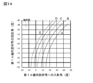
- FIG. 14 is a graph showing the relationship between the incident angle of light on the first A deflection member or the second A deflection member and the diffraction angle of the first A deflection member or the second A deflection member, using the pitch d as a parameter.
- a point on the light guide plate where light emitted from the center point of the image forming region of the image forming device collides with the light guide plate is guided to the first direction through the origin and the origin.
- the axis of the optical plate is the X axis
- the thickness direction axis of the light guide plate passing through the origin is the Z axis
- the X axis and the axis perpendicular to the Z axis are the Y axis
- the first deflection unit and the second deflection unit are: It can be set as the form arrange
- the first A deflection member and the second A deflection member are composed of a volume hologram diffraction grating,
- the wave vector having a first 1A deflecting member and k v 1A, and the X component of k v 1A, Y component, the Z component k X 1A, k Y 1A, and k Z 1A
- the wave vector of the 2A deflection member is k v 2-A
- the X component, Y component, and Z component of k v 2-A are k X 2-A , k Y 2-A , k Z 2-A .
- the first C deflection member and the second C deflection member are composed of a volume hologram diffraction grating,
- the wave vector having a second 1C deflecting member and k v 1C, and X components of k v 1C, Y component, the Z component k X 1C, k Y 1C, and k Z 1C,
- the wave vector of the second C deflection member is k v 2-C
- the X component, Y component, and Z component of k v 2-C are k X 2-C , k Y 2-C , and k Z 2-C .
- the first B deflection member and the second B deflection member are composed of a volume hologram diffraction grating,
- the wave vector having a first 1B deflecting member and k v 1B, and the X component of k v 1B, Y component, the Z component k X 1B, k Y 1B, and k Z 1B,
- the wave vector of the second B deflection member is k v 2-B
- the X component, Y component, and Z component of k v 2-B are k X 2-B , k Y 2-B , k Z 2-B .
- the volume hologram diffraction grating is a transmission type, depending on the arrangement of the first A deflection member, the first B deflection member, the first C deflection member, the second A deflection member, the second B deflection member, and the second C deflection member with respect to the light guide plate. Alternatively, it may be a reflection type.
- the volume hologram diffraction grating means a hologram diffraction grating that diffracts only + 1st order diffracted light.
- the first A deflection member and the second A deflection member may be partially overlapped.
- the first A deflection member has an end portion in the X direction
- the second A deflection member has an end portion in the -X direction, but the end portion in the X direction of the first A deflection member and the second A deflection member It can be configured such that the end in the ⁇ X direction overlaps.
- the first A deflection member and the first B deflection member are laminated, and the second A deflection member and the second B deflection member are laminated. It can be in the form.
- the first B deflecting member and the first C deflecting member are laminated, and the second B deflecting member and the second C deflecting member can be laminated, or the first A deflecting member and the first B deflecting member can be formed.
- the member and the first C deflection member are stacked, and the second A deflection member, the second B deflection member, and the second C deflection member may be stacked.
- the 1A deflection member, the 1B deflection member, and the 1C deflection member are composed of a volume hologram diffraction grating,
- the average diffraction efficiency of the 1A deflection member with respect to the light emitted from the image forming apparatus is ⁇ 1-A
- the average diffraction efficiency of the 1B deflection member is ⁇ 1-B
- the average diffraction efficiency of the 1C deflection member is ⁇ 1-C.
- the 2A deflection member, the 2B deflection member, and the 2C deflection member are composed of a volume hologram diffraction grating
- the average diffraction efficiency of the 2A deflection member for the light emitted from the image forming apparatus is ⁇ 2-A
- the average diffraction efficiency of the 2B deflection member is ⁇ 2 -B
- the average diffraction efficiency of the 2C deflection member is ⁇ 2 -C.
- the diffraction efficiency ⁇ is defined as I 1 / I when the light intensity of light incident on the volume hologram diffraction grating is I 0 and the light intensity of the + 1st order diffracted light diffracted by the volume hologram diffraction grating is I 1 . It is represented by I0 .
- the diffraction efficiency can be controlled by, for example, the thickness of the volume hologram diffraction grating.
- the value of the diffraction efficiency ⁇ becomes lower. Further, the value of the diffraction efficiency ⁇ decreases as the refractive index modulation degree ⁇ n in the volume hologram diffraction grating increases.
- the volume closest to the light incident portion of the volume hologram diffraction grating LI 1 is the amount of light emitted from the hologram diffraction grating region
- LI 2 is the amount of light emitted from the next closest volume hologram diffraction grating region
- LI 4 is the amount of light emitted from the fourth volume hologram diffraction grating region
- LI 3 (1.0 ⁇ 0.2 ⁇ 0.16)
- ⁇ 0.2 0.128
- first A deflection member and the second A deflection member are collectively referred to as “first A deflection member etc.”, and the first B deflection member and the second B deflection member are collectively referred to as “first The first C deflection member and the second C deflection member may be collectively referred to as “first C deflection member”.
- the light emitted from the center point of the image forming area of the image forming apparatus is vertically incident on the first A deflection member and the second A deflection member. It is also possible to adopt a configuration in which the light is incident at a certain angle that is not vertical.
- the refractive index of the material constituting the light guide plate can be 1.5 or more, preferably 1.6 or more
- the material constituting the volume hologram diffraction grating can have a refractive index of 1.5 or more, preferably 1.6 or more.
- the optical device is a transflective type (see-through type). Specifically, at least a portion of the optical device facing the eyeball (pupil) of the observer is made semi-transmissive (see-through), and this portion of the optical device (specifically, at least the first C deflection member and the second C deflection member). You can see the outside view through.
- semi-transmissive does not mean that half (50%) of the incident light is transmitted or reflected, but a part of the incident light is transmitted and the rest is reflected. It is used to mean.
- the image display device or display device of the present disclosure can display a single color (for example, green) image.
- P 3 and three types of red, green, and blue.
- a P-layer diffraction grating layer composed of a volume hologram diffraction grating can be laminated. Each diffraction grating layer is formed with interference fringes corresponding to one type of wavelength band (or wavelength).
- a first A deflection member, a first B deflection member, etc., and a first C consisting of one diffraction grating layer It can also be set as the structure by which the P type interference fringe is formed in the deflection
- a first B deflection member such as a first A deflection member composed of a diffraction grating layer composed of a volume hologram diffraction grating that diffracts and reflects light having a red wavelength band (or wavelength) on the first light guide plate.
- 1A deflection member comprising a diffraction grating layer comprising a volume hologram diffraction grating, which includes a member, a first C deflection member, and the like, and diffracts light having a green wavelength band (or wavelength) on the second light guide plate
- the first B deflection member and the first C deflection member are arranged, and the third light guide plate is composed of a diffraction grating layer composed of a volume hologram diffraction grating that diffracts light having a blue wavelength band (or wavelength).
- a first A deflecting member composed of a diffraction grating layer composed of a volume hologram diffraction grating that diffracts and reflects light having a red wavelength band (or wavelength) on one surface of the first light guide plate, etc.
- a diffraction grating layer comprising a volume hologram diffraction grating that diffracts light having a green wavelength band (or wavelength) on the other surface of the first light guide plate by arranging the 1B deflection member and the 1C deflection member, etc.
- a volume hologram diffraction grating in which a first light deflecting member, a first light deflecting member, and a first light deflecting member are arranged to diffract light having a blue wavelength band (or wavelength) on the second light guide plate.
- a structure in which a first A deflection member, a first B deflection member, a first C deflection member, and the like composed of a diffraction grating layer composed of the above are arranged, and the first light guide plate and the second light guide plate are stacked with a gap therebetween.
- Adopt Good Adopt Good.
- a first A deflecting member composed of a diffraction grating layer made of a volume hologram diffraction grating that diffracts and reflects light having a red wavelength band (or wavelength) on one surface of the light guide plate, etc.
- 1B deflection member, etc. comprising a 1B deflection member, 1C deflection member, etc.
- a diffraction grating layer comprising a volume hologram diffraction grating that diffracts light having a green wavelength band (or wavelength), etc.
- 1A composed of a diffraction grating layer made of a volume hologram diffraction grating that diffracts light having a blue wavelength band (or wavelength) on the other surface of the light guide plate by laminating a member, etc. and a 1C deflection member, etc.
- a structure in which a deflection member, a 1B deflection member, a 1C deflection member, and the like are arranged may be employed.
- P kinds of volume hologram diffraction gratings can be formed in one diffraction grating layer.
- the diffraction efficiency is increased when light having each wavelength band (or wavelength) is diffracted by the 1A deflection member, the 1B deflection member, and the 1C deflection member. It is possible to increase the diffraction acceptance angle and optimize the diffraction angle. It is preferable to arrange a protective member so that the volume hologram diffraction grating does not directly contact the atmosphere.
- volume hologram diffraction grating As a material constituting the volume hologram diffraction grating, a photopolymer material can be mentioned.
- the constituent material and basic structure of the volume hologram diffraction grating in the optical device and the like of the present disclosure may be the same as those of the conventional volume hologram diffraction grating.
- interference fringes are formed from the inside to the surface. The method of forming such interference fringes may be the same as the conventional forming method.
- a material (for example, photopolymer material) constituting a volume hologram diffraction grating is irradiated with object light from a first predetermined direction on one side, and at the same time, a volume hologram diffraction grating is formed.
- the reference light is irradiated from the second predetermined direction on the other side to the material to be recorded, and the interference fringes formed by the object light and the reference light may be recorded inside the material constituting the volume hologram diffraction grating.
- the inclination angle of the interference fringes means an angle formed between the surface of the volume hologram diffraction grating and the interference fringes.
- a diffraction grating layer is formed by separately forming P diffraction grating layers and then forming P diffraction grating layers.
- the photopolymer material having adhesiveness is sequentially attached thereon to produce a diffraction grating layer, whereby the P layer A diffraction grating layer may be produced.
- the inclination angle (slant angle) of the interference fringes may be constant in the volume hologram diffraction grating, or may be changed depending on the value of the angle of view of the image incident on the volume hologram diffraction grating.
- it may be changed continuously or may be changed stepwise.
- the material constituting the volume hologram diffraction grating includes at least a photopolymerizable compound, a binder resin, and a photopolymerization initiator.
- a photopolymerizable compound for example, known photopolymerizable compounds such as acrylic monomers, methacrylic monomers, styrene monomers, butadiene monomers, vinyl monomers, and epoxy monomers can be used. These may be copolymers, monofunctional or polyfunctional. Moreover, these monomers may be used alone or in combination. Any known binder resin can be used.
- cellulose acetate resin acrylic resin, acrylic ester resin, methacrylic acid resin, epoxy resin, urethane resin, polypropylene resin, polyvinyl ether Resin, polycarbonate resin, polyamide resin, polyvinyl acetate, vinyl chloride resin, urea resin, styrene resin, butadiene resin, natural rubber resin, polyvinyl carbazole, polyethylene glycol, phenol resin, or co-polymer of these Examples include coalescence and gelatin.
- the binder resin may be used alone or in combination. Any known photopolymerization initiator can be used.
- a photoinitiator may be used individually, may be used in multiple, and may be used in combination with multiple or single photosensitizing dye.
- a plasticizer for protecting the volume hologram diffraction grating
- any material can be used as long as it is transparent. Even if it is formed by coating, the material formed in advance is a photosensitive material precursor layer. May be laminated.
- a material constituting the protective layer for example, polyvinyl alcohol (PVA) resin, acrylic resin, polyurethane resin, polyethylene terephthalate (PET) resin, triacetyl cellulose (TAC) resin, polymethyl methacrylate (PMMA) resin, polypropylene resin , Polycarbonate resin and polyvinyl chloride resin.
- the image forming device may have a plurality of pixels arranged in a two-dimensional matrix. Note that such a configuration of the image forming apparatus is referred to as a “first image forming apparatus” for convenience.
- an image forming apparatus having the first configuration for example, an image forming apparatus including a reflective spatial light modulator and a light source; an image forming apparatus including a transmissive spatial light modulator and a light source; an organic EL (Electro-Luminescence) element And an image forming apparatus composed of a light emitting element such as an inorganic EL element, a light emitting diode (LED), a semiconductor laser element, etc., among others, an image forming apparatus composed of a reflective spatial light modulator and a light source, Or it is preferable to set it as the image forming apparatus comprised from the organic EL element.
- the spatial light modulator examples include a light valve, for example, a transmissive or reflective liquid crystal display device such as LCOS (Liquid Crystal On On Silicon), a digital micromirror device (DMD), and a light emitting element as a light source. be able to.
- the reflective spatial light modulator reflects a part of light from the liquid crystal display device and the light source to the liquid crystal display device, and passes a part of the light reflected by the liquid crystal display device.
- a polarization beam splitter that leads to the optical system can be used.
- Examples of the light emitting element that constitutes the light source include a red light emitting element, a green light emitting element, a blue light emitting element, and a white light emitting element, or red light emitted from the red light emitting element, the green light emitting element, and the blue light emitting element.
- white light may be obtained by mixing green light and blue light with a light pipe and performing luminance uniformity.
- Examples of the light emitting element include a semiconductor laser element, a solid state laser, and an LED.
- the number of pixels may be determined based on specifications required for the image display device. Specific values of the number of pixels are 320 ⁇ 240, 432 ⁇ 240, 640 ⁇ 480, 1024 ⁇ 768, 1920 ⁇ 1080, and the like. Can be illustrated.
- the image forming apparatus includes a light source and a scanning unit that scans the parallel light emitted from the light source. It can be in the form. Note that such a configuration of the image forming apparatus is referred to as a “second configuration image forming apparatus” for convenience.
- Examples of the light source in the image forming apparatus having the second configuration include a light emitting element, and specifically include a red light emitting element, a green light emitting element, a blue light emitting element, and a white light emitting element, or a red light emitting element.
- White light may be obtained by mixing red light, green light, and blue light emitted from the element, the green light emitting element, and the blue light emitting element by using a light pipe and performing luminance equalization.
- Examples of the light emitting element include a semiconductor laser element, a solid state laser, and an LED.
- the number of pixels (virtual pixels) in the image forming apparatus having the second configuration may be determined based on specifications required for the image display apparatus.
- the number of pixels 320 ⁇ 240, 432 ⁇ 240, 640 ⁇ 480, 1024 ⁇ 768, 1920 ⁇ 1080 and the like can be exemplified.
- the scanning unit include a MEMS (Micro Electro Mechanical Systems) or a galvano mirror that performs micro scanning that can rotate in a two-dimensional direction.
- an optical system which is an optical system that converts the emitted light from the image forming apparatus into parallel light, may be referred to as a “parallel light emitting optical system”, Specifically, for example, a plurality of parallel light beams made by a collimating optical system or a relay optical system are made incident on the light guide plate. This is based on the fact that the light wavefront information when entering the light guide plate needs to be preserved even after being emitted from the light guide plate through the first A deflection member, the first B deflection member, and the first C deflection member.
- the light emitting part of the image forming apparatus may be positioned at the position (position) of the focal length in the parallel light emitting optical system, for example. .
- the parallel light emission optical system has a function of converting pixel position information into angle information in the optical system of the optical device.
- an optical system having a positive optical power as a whole which is a single lens or a combination of a convex lens, a concave lens, a free-form surface prism, and a hologram lens, can be exemplified.
- an appropriate light guiding means is provided between the parallel light emitting optical system, the first A deflection member, and the second A deflection member. What is necessary is just to arrange
- a reflecting mirror can be mentioned as a light guide means. Further, the light emitted from the parallel light emission optical system may be directly condensed on the first A deflection member and the second A deflection member.
- the light guide plate has two parallel surfaces (a first surface and a second surface).
- the light guide plate entrance surface When the surface of the light guide plate on which light is incident is the light guide plate entrance surface, and the surface of the light guide plate on which light is emitted is the light guide plate exit surface, the light guide plate entrance surface and the light guide plate exit surface are configured by the first surface.
- the light guide plate entrance surface may be configured by the first surface
- the light guide plate exit surface may be configured by the second surface.
- glass containing optical glass such as quartz glass or BK7, or plastic material (for example, PMMA, polycarbonate resin, acrylic resin, amorphous polypropylene resin, styrene resin containing AS resin)
- plastic material for example, PMMA, polycarbonate resin, acrylic resin, amorphous polypropylene resin, styrene resin containing AS resin
- the shape of the light guide plate is not limited to a flat plate, and may have a curved shape.
- a material having a refractive index of 1.5 or more BK7, polycarbonate resin, amorphous polypropylene resin, styrene resin including AS resin can be exemplified, and as a material having a refractive index of 1.6 or more, An acrylyl resin can be exemplified.
- the image display device may include a light control device. That is, the optical device may overlap at least a part of the light control device. More specifically, it is preferable that at least the first C deflection member and the like of the optical device overlap with the light control device.
- the light control device A first substrate, A second substrate facing the first substrate; A first transparent electrode provided on the facing surface of the first substrate facing the second substrate; A second transparent electrode provided on the facing surface of the second substrate facing the first substrate, and A light control layer sandwiched between the first transparent electrode and the second transparent electrode, It can be set as the form which consists of. Note that a higher voltage than that of the second transparent electrode is applied to the first transparent electrode, for example, during the operation of the dimmer.
- the light control layer may be formed of an optical shutter that applies a color change of a substance generated by a redox reaction of an inorganic or organic electrochromic material.
- the light control layer can be in a form containing an inorganic or organic electrochromic material.
- the light control layer can be formed from the first transparent electrode side by a WO 3 layer / Ta 2 O 5 layer /
- a laminated structure of an inorganic electrochromic material layer such as an Ir x Sn 1-x O layer or a laminated structure of an inorganic electrochromic material layer such as a WO 3 layer / Ta 2 O 5 layer / IrO x layer is adopted. it can.
- a MoO 3 layer or a V 2 O 5 layer can be used instead of the WO 3 layer.
- a ZrO 2 layer and a zirconium phosphate layer can be used, or a Prussian blue complex / nickel-substituted Prussian blue complex or the like can also be used.
- the organic electrochromic material for example, the electrochromic material disclosed in Japanese Patent Application Laid-Open Nos. 2014-111710 and 2014-159385 can be used.
- the light control layer can be configured to contain an electrophoretic dispersion, and the light control device can apply an electrodeposition / dissociation phenomenon generated by a reversible oxidation-reduction reaction of a metal (for example, silver particles).
- the light shutter by the electrodeposition method electroposition / field deposition
- the light control layer can also be configured to include an electrolyte containing metal ions.
- the electrophoretic dispersion liquid is composed of a large number of charged electrophoretic particles and a dispersion medium having a color different from that of the electrophoretic particles.
- the electrophoretic particles are negatively charged, relative to the first transparent electrode
- the negatively charged electrophoretic particles migrate so as to cover the second transparent electrode. Therefore, the light shielding rate in the light control device is a high value.
- the electrophoretic particles cover the first transparent electrode. Run. Therefore, the light shielding rate in the light control device is a low value.
- the voltage may be a direct current or an alternating current.
- the shape of the patterned first transparent electrode is such that when the electrophoretic particles migrate so as to cover the first transparent electrode and the light shielding rate in the light control device becomes a low value, the value of the light shielding rate in the light control device is optimum. It is sufficient to make it a shape that can be realized, and it may be determined by performing various tests.
- an insulating layer may be formed on the transparent electrode.
- the material constituting the insulating layer include a colorless and transparent insulating resin. Specifically, for example, an acrylic resin, an epoxy resin, a fluorine resin, a silicone resin, a polyimide resin, A polystyrene resin etc. can be mentioned.
- a transparent glass substrate such as soda lime glass and white plate glass
- a plastic substrate such as soda lime glass and white plate glass
- a plastic substrate such as soda lime glass and white plate glass
- a plastic substrate such as soda lime glass and white plate glass
- a plastic substrate such as soda lime glass and white plate glass
- a plastic substrate such as soda lime glass and white plate glass
- a plastic substrate such as soda lime glass and white plate glass
- a plastic substrate such as soda lime glass and white plate glass
- plastic substrate such as soda lime glass and white plate glass
- plastic substrate such as soda lime glass and white plate glass
- plastic substrate such as soda lime glass and white plate glass
- plastic substrate such as soda lime glass and white plate glass
- plastic substrate such as soda lime glass and white plate glass
- a plastic substrate such as soda lime glass and white plate glass
- a plastic substrate such as soda lime glass and white plate glass
- a plastic substrate such as soda lime glass and white plate glass
- a plastic substrate such as soda lime glass and white plate glass
- a plastic substrate such as soda lime
- the plastic sheet and the plastic film may have a rigidity that does not easily bend, or may have flexibility.
- a barrier layer made of an inorganic material or an organic material may be formed on the inner surface of the substrate.
- sealing members also called sealing agents, epoxy resins, urethane resins, acrylic resins, vinyl acetate resins, ene-thiol resins, silicone resins, modified polymer resins, etc.
- sealing agents also called sealing agents, epoxy resins, urethane resins, acrylic resins, vinyl acetate resins, ene-thiol resins, silicone resins, modified polymer resins, etc.
- Various resins such as a moisture curable type and an anaerobic curable type can be used.
- one of the substrates constituting the light control device also serves as a component of the optical device (specifically, a protective member disposed so that the volume hologram diffraction grating is not in direct contact with the atmosphere), the entire display device The weight of the display device can be reduced, and there is no possibility that the user of the display device feels uncomfortable. Note that the other substrate can be thinner than the other substrate.
- the first transparent electrode may be patterned or may not be patterned.
- the second transparent electrode may also be patterned or may not be patterned.
- indium-tin composite oxide including ITO, Indium Tin Oxide, Sn-doped In 2 O 3 , crystalline ITO, and amorphous ITO is used as a material constituting the first transparent electrode and the second transparent electrode.
- Fluorine-doped SnO 2 FTO
- IFO F-doped In 2 O 3
- antimony-doped SnO 2 ATO
- SnO 2 ZnO (including Al-doped ZnO and B-doped ZnO), indium-zinc composite
- oxides IZO, Indium Zinc Oxide
- spinel oxides oxides having a YbFe 2 O 4 structure
- conductive polymers such as polyaniline, polypyrrole, and polythiophene.
- two or more of these can be used in combination.
- the first transparent electrode and the second transparent electrode are formed based on a physical vapor deposition method (PVD method) such as a vacuum vapor deposition method or a sputtering method, various chemical vapor deposition methods (CVD method), various coating methods, and the like.
- PVD method physical vapor deposition method
- CVD method chemical vapor deposition methods
- Patterning can be performed by an arbitrary method such as an etching method, a lift-off method, or a method using various masks.
- the light control device may be arranged in the front part. And in this case, the front part has a rim; the light control device can be configured to be fitted into the rim. Further, in the display device of the present disclosure including the various preferable embodiments described above, the optical device and the light control device may be arranged in this order from the observer side, or the light control device and the optical device may be arranged in this order. Also good.
- An illuminance sensor that measures the illuminance of the environment where the display device is placed is further provided; a mode for controlling the light shielding rate of the light control device based on the measurement result of the illuminance sensor (environmental illuminance measurement sensor) It can be.
- it further includes an illuminance sensor (environmental illuminance measurement sensor) for measuring the illuminance of the environment where the display device is placed; formed by the image forming apparatus based on the measurement result of the illuminance sensor (environmental illuminance measurement sensor). It is possible to control the luminance of the image.
- the apparatus further includes a second illuminance sensor (sometimes referred to as “transmitted light illuminance measurement sensor” for convenience) that measures illuminance based on light transmitted through the light control device from the external environment; Based on the measurement result of the (transmitted light illuminance measurement sensor), the light shielding rate of the light control device can be controlled.
- the apparatus further includes a second illuminance sensor (transmitted light illuminance measurement sensor) that measures illuminance based on light transmitted through the light control device from the external environment; measurement result of the second illuminance sensor (transmitted light illuminance measurement sensor) Based on the above, it is possible to control the luminance of the image formed by the image forming apparatus.
- the second illuminance sensor (transmitted light illuminance measurement sensor) is arranged closer to the viewer than the optical device.
- At least two second illuminance sensors (transmitted light illuminance measurement sensors) are arranged to measure illuminance based on light that has passed through a portion with a high light shielding rate, and to measure illuminance based on light that has passed through a portion with a low light shielding rate. You may go. These forms may be combined. Furthermore, you may combine these forms and the form which controls based on the measurement result of said illuminance sensor (environmental illuminance measurement sensor).
- the illuminance sensor (environmental illuminance measurement sensor, transmitted light illuminance measurement sensor) may be configured from a known illuminance sensor, and the illuminance sensor may be controlled based on a known control circuit.
- the maximum light transmittance of the light control device can be 50% or more, and the minimum light transmittance of the light control device can be 30% or less.
- the upper limit value of the maximum light transmittance of the light control device can be 99%, and the lower limit value of the minimum light transmittance of the light control device can be 1%.
- a control circuit (a light control device / control circuit for controlling the light shielding rate of the light control device) by attaching a connector to the light control device (specifically, a connector attached to the first transparent electrode or the second transparent electrode)
- the light control device may be electrically connected to the control device for controlling the image forming apparatus via the connector and the wiring.
- the light passing through the light control device may be colored to a desired color by the light control device.
- the color colored by the light control device can be variable, or the color colored by the light control device can be fixed.
- a light control device colored in red, a light control device colored in green, and a light control device colored in blue may be stacked.
- the color to be colored by the light control device is not limited, but can be exemplified by brown.
- the observer observes the brightness of the light that has passed through the light control device and the optical device, and the observer manually controls and adjusts the light blocking rate by operating switches, buttons, dials, sliders, knobs, etc.
- the light shielding rate is controlled and adjusted based on the measurement result of the second illuminance sensor (transmitted light illuminance measurement sensor) that measures the illuminance based on the light transmitted through the light control device from the external environment. be able to.
- the control and adjustment of the light shielding rate may be performed by controlling the voltage applied to the first transparent electrode and the second transparent electrode.
- At least two second illuminance sensors are arranged to measure illuminance based on light that has passed through a portion with a high light shielding rate, and to measure illuminance based on light that has passed through a portion with a low light shielding rate. You may go.
- the display device may include one image display device or two image display devices. When two image display devices are provided, the voltage applied to the first transparent electrode and the second transparent electrode is adjusted in each of the one light control device and the other light control device, so that one of the light control devices And the light shielding rate of the other light control device can be equalized.
- the light blocking rate in one light control device and the light blocking rate in the other light control device are, for example, a second illuminance sensor (transmitted light illuminance measurement sensor) that measures illuminance based on the light transmitted through the light control device from the external environment described above. Or the brightness of the light passing through one light control device and the optical device and the light brightness passing through the other light control device and the optical device.
- the observer can also control and adjust manually by operating switches, buttons, dials, sliders, knobs, and the like.
- a test pattern may be displayed on the optical device.
- the frame may include a front portion disposed in front of the observer and two temple portions that are rotatably attached to both ends of the front portion via hinges. it can. A modern portion is attached to the tip of each temple portion.
- the image display device is attached to the frame, specifically, for example, the image forming device may be attached to the upper portion of the front portion.
- the front part and the two temple parts can be integrated. That is, when the entire display device of the present disclosure is viewed, the frame has substantially the same structure as normal glasses.
- the material constituting the frame including the pad portion can be made of the same material as that constituting normal glasses such as metal, alloy, plastic, and a combination thereof.
- the nose pad can be set as the structure by which the nose pad is attached to the front part. That is, when the entire display device of the present disclosure is viewed, the assembly of the frame (including the rim) and the nose pad has substantially the same structure as normal glasses.
- the nose pad can also have a known configuration and structure.
- each image forming apparatus includes a headphone section, and the headphone section wiring from each image forming apparatus is routed from the tip of the modern section to the headphone section via the temple section and the interior of the modern section. It can also be made into the extended form.
- the headphone unit include an inner ear type headphone unit and a canal type headphone unit.
- the headphone part wiring preferably has a form extending from the tip part of the modern part to the headphone part so as to wrap around the back side of the auricle (ear shell). Moreover, it can also be set as the form by which the imaging device was attached to the center part of the front part.
- the imaging device is configured by a solid-state imaging device and a lens made up of, for example, a CCD or a CMOS sensor.
- the wiring from the imaging device may be connected to, for example, one image display device (or image forming device) via the front portion, and is further included in the wiring extending from the image display device (or image forming device). That's fine.
- a head-mounted display can be configured by the display device of the present disclosure. This makes it possible to reduce the weight and size of the display device, significantly reduce discomfort when the display device is mounted, and further reduce the manufacturing cost.
- the image display device of the present disclosure can be applied to a head-up display (HUD) provided in a cockpit of a vehicle or an aircraft.
- HUD head-up display
- the virtual image formation region where a virtual image is formed based on the light emitted from the image forming apparatus can be a HUD disposed on a windshield of a cockpit of a vehicle or an aircraft, or image formation
- a combiner having a virtual image forming area in which a virtual image is formed based on light emitted from the apparatus may be a HUD arranged on a windshield of a vehicle or an aircraft cockpit.
- Example 1 relates to an optical device of the present disclosure, an image display device of the present disclosure, and a display device of the present disclosure.
- FIG. 1A shows a schematic perspective view of the optical device of Example 1
- FIG. 1B shows a schematic view of the optical device of Example 1 viewed from above.
- FIG. 2 shows a schematic perspective view of the first deflection unit constituting the optical device of Example 1
- FIG. 3 shows a schematic perspective view of the second deflection unit.
- 4A shows a schematic cross-sectional view
- FIG. 4B shows a schematic view of the optical device of Example 1 viewed from the side
- FIG. 6 shows a schematic view of the display device of Example 1 viewed from above.
- a schematic view of the display device of Example 1 as viewed from the front is shown in FIG.
- conceptual diagrams such as wave number vectors of the 1A deflection member, the 1B deflection member, and the 1C deflection member are shown in FIGS. 10A, 10B, 11A, and 11B
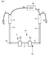
- the optical device 10 is an optical device in which light emitted from the image forming apparatus 60 is incident, guided, and emitted.
- the first deflection unit includes a first A deflection member 31, a first B deflection member 32, and a first C deflection member 33.
- the second deflection unit includes a second A deflection member 41, a second B deflection member 42, and a second C deflection member 43.
- a part of the light emitted from the image forming apparatus 60 is incident on the first A deflection member 31,
- the light incident on the first A deflection member 31 is deflected by the first A deflection member 31, is totally reflected inside the light guide plate 20, enters the first B deflection member 32, is deflected by the first B deflection member 32, and is guided by the light guide plate.
- 20 is totally reflected to enter the first C deflection member 33, is deflected by the first C deflection member 33, and is emitted toward the pupil 90 of the observer.
- At least the remaining part of the light emitted from the image forming apparatus 60 is incident on the second A deflection member 41,
- the light incident on the second A deflection member 41 is deflected by the second A deflection member 41, totally reflected inside the light guide plate 20, enters the second B deflection member 42, is deflected by the second B deflection member 42, and is guided to the light guide plate.
- 20 is totally reflected to enter the second C deflection member 43, is deflected by the second C deflection member 43, and is emitted toward the pupil 90 of the observer.
- the direction when the light propagation direction deflected by the first A deflection member 31 is orthogonally projected onto the light guide plate 20 is the first direction
- the propagation direction of the light deflected by the second A deflection member 41 is orthogonally projected onto the light guide plate 20.
- the first direction is the opposite direction to the second direction, where the second direction is the second direction.
- the image display device 11 includes: Image forming apparatus 60, and
- the optical device includes an optical device that receives, guides, and emits light emitted from the image forming apparatus 60.
- the optical device includes the optical device 10 of the first embodiment.
- the display device of Example 1 is A frame 50 attached to the observer's head; and An image display device 11 attached to the frame 50; With
- the image display device 11 includes an image forming device 60 and an optical device that receives, guides, and emits light emitted from the image forming device 60.
- the optical device includes the optical device 10 of the first embodiment.
- the display device of the first embodiment is specifically a binocular type including two image display devices 11, but may be a single eye type including one.
- the optical device 10 is a see-through type (semi-transmissive type).
- the image forming apparatus 60 displays a single color image, but the present invention is not limited to this.
- a point on the light guide plate 20 where light emitted from the image formation region center point of the image forming device 60 collides with the light guide plate 20 passes through the origin O, the origin O, and the first point.
- the axis of the light guide plate 20 facing the direction 1 is the X axis
- the thickness direction axis of the light guide plate 20 passing through the origin O is the Z axis, X axis, and Z axis.
- the first deflection unit and the second deflection unit are arranged symmetrically on the YZ plane.
- the light emitted from the center point of the image forming area of the image forming apparatus 60 is perpendicularly incident on the first A deflection member 31 and the second A deflection member 41.
- the present invention is not limited to this, and may be configured to enter the first A deflection member 31 and the second A deflection member 41 at a certain angle that is not vertical.
- the first A deflection member 31 has an end portion in the X direction
- the second A deflection member 41 has an end portion in the -X direction
- the end surface of the second A deflection member 41 in the ⁇ X direction are in contact with each other.
- the optical apparatus according to the first embodiment specifically, half of the light emitted from the image forming apparatus 60 is incident on the first A deflection member 31 and the second A deflection member 41 has an image. The remaining half of the light emitted from the forming device 60 is incident.
- light propagating through the first deflection unit is indicated by a thin solid line
- light propagating through the second deflection unit is indicated by a thin dotted line.
- light propagating from the upper side to the lower side of the page is indicated by a symbol in which a “x” mark is put in a circle.
- the light is emitted from the center point of the image forming area of the image forming apparatus 60, enters the first A deflection member 31 and the second A deflection member 41, and exits from the first C deflection member 33 and the second C deflection member 43.
- the light is emitted from the central point of the image forming area of the image forming apparatus 60, enters the first A deflection member 31 and the second A deflection member 41, totally reflects the inside of the light guide plate 20, and the first C Light emitted from the deflection member 33 and the second C deflection member 43 is indicated by a thick solid line, and is emitted from the image forming area of the image forming apparatus 60 at an angle of view ( ⁇ ) and an angle of view ( ⁇ ).
- the light incident on the second A deflection member 41, totally reflected inside the light guide plate 20, and emitted from the first C deflection member 33 and the second C deflection member 43 is indicated by a thick dotted line.
- the first A deflection member 31, the first B deflection member 32, the first C deflection member 33, the second A deflection member 41, the second B deflection member 42, and the second C deflection member 43 are volume hologram diffraction gratings. Consists of.
- the light guide plate 20 has two parallel surfaces (a first surface 21 and a second surface 22).
- the light guide plate incident surface of the light guide plate 20 is configured by the first surface 21, and the second surface 22.
- the light guide plate exit surface of the light guide plate 20 is configured.
- the first A deflection member 31 and the second A deflection member 41 made of a transmission type volume hologram diffraction grating are disposed on the first surface 21 of the light guide plate 20 (specifically, bonded),
- the first B deflecting member 32, the first C deflecting member 33, the second B deflecting member 42, and the second C deflecting member 43 made of a reflective volume hologram diffraction grating are disposed on the second surface 22 of the light guide plate 20 (specifically). In fact, it is glued).
- the first A deflecting member 31, the first B deflecting member 32, the first C deflecting member 33, the second A deflecting member 41, the second B deflecting member 42, and the second C deflecting member 43 are composed of one diffraction grating layer.
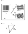
- Each deflecting member made of a photopolymer material is formed with interference fringes corresponding to one type of wavelength band (or wavelength), and is produced by a conventional method.
- the pitch of the interference fringes formed on the deflecting member (diffractive optical element) is constant, and the interference fringes are linear.
- the inclination angle (slant angle) of the interference fringes may be constant in the volume hologram diffraction grating, or may be changed depending on the value of the angle of view of the image incident on the volume hologram diffraction grating.
- it may be changed continuously or may be changed stepwise.
- the diffraction efficiency of the first A deflection member 31 and the diffraction efficiency of the second A deflection member 41 are sandwiched between the boundary region between the end surface of the first A deflection member 31 in the X direction and the end face of the second A deflection member 41 in the ⁇ X direction. It is preferable to design the first A deflection member 31 and the second A deflection member 41 so that the current continuously changes.
- ⁇ diff is required to be larger than the total reflection angle.
- the diffraction angle with respect to the angle of view of the image is defined by an equation that satisfies the Bragg condition described later, and is determined by the wavelength ⁇ and the pitch d of the grating surface.
- the graph of FIG. 14 shows the relationship between the incident angle of light on the first A deflection member 31 or the second A deflection member 41 and the diffraction angle of the first A deflection member 31 or the second A deflection member 41 using the pitch d as a parameter. .
- FIG. 14 shows the relationship between the incident angle of light on the first A deflection member 31 or the second A deflection member 41 and the diffraction angle of the first A deflection member 31 or the second A deflection member 41 using the pitch d as a parameter. .
- Data of 360 nm is shown
- the diffraction angle ⁇ diff with respect to the angle of view of the image is expressed by the above formula.
- the value of m is preferably “ ⁇ 1” ( ⁇ 1 order), and the incident angle of view corresponds to a diffraction angle of ⁇ 90 degrees from the total reflection angle (see FIG. 14).
- the first A deflection member 31 and the second A deflection member 41 share the angle of view in the X direction and the ⁇ X direction, respectively, but it is preferable that the assigned angle of view overlap.
- the pitch 14 shows the relationship between the pitch d and the diffraction angle when the wavelength is 530 nm in the first A deflection member 31 or the second A deflection member 41.
- a pitch at which the incident angle of view overlaps such as “D” or “E” with 0 degree as a boundary.
- the width of the deflection member may be set in consideration.
- the width of the deflecting member (specifically, the width along the X direction of the first A deflecting member 31 and the width along the ⁇ X direction of the second A deflecting member 41) may be set so as to satisfy the following equation. For example, when the half-wave width of a light source composed of LEDs is 30 nm, the range of 500 nm to 560 nm is calculated, and the minimum deflection member width is set, or the maximum angle of the diffraction angle ⁇ diff is set. Is preferred.
- an image incident on the light guide plate 20 extends in the X-axis direction and the ⁇ X-axis direction ( Enlarged). Further, when light propagates through the interior of the light guide plate 20 from the 1B deflection member or the like toward the 1C deflection member or the like by total reflection, an image expanded (enlarged) in the X-axis direction and the ⁇ X-axis direction is Further, it is extended in the ⁇ Y axis direction. In this way, the image from the image forming apparatus 60 is expanded (enlarged) in the vertical and horizontal directions and reaches the observer's pupil 90.
- the parallel light from the image forming apparatus 60 is diffracted by the 1A deflection member and the 1B deflection member (specifically, diffracted and reflected a plurality of times), and the inside of the light guide plate 20 is totally reflected. It propagates and is emitted from the second surface 22 from the light guide plate 20 as parallel light.
- a surface not facing the light guide plate 20 such as the first A deflection member, the first B deflection member, and the first C deflection member is covered with a transparent resin plate or a transparent resin film, and the first A deflection member, etc. It is good also as a structure which prevents that a member etc. and a 1C deflection
- a transparent protective film may be bonded to the first surface 21 or the second surface 22 of the light guide plate 20 to protect the light guide plate 20.
- planar shapes of the first A deflection member and the first C deflection member are rectangular
- the planar shape of the 1B deflection member and the like is an isosceles trapezoid.
- the planar shape of these members is not limited to these.
- the planar shape of the 1A deflection member or the like may be circular
- the planar shape of the 1B deflection member or the like may be rectangular.
- the planar shape of the light guide plate 20 may be a shape in which a corner is notched.
- the material constituting the light guide plate 20 is made of glass having a thickness of 1.0 mm (refractive index: 1.51), a photopolymer material constituting the first A deflection member, the first B deflection member, the first C deflection member, etc.
- the average refractive index was 1.51.
- the thickness of the light guide plate 20 does not essentially contribute to widening the angle of view of the display image, but the thickness of the light guide plate 20 is reduced to reduce the size of the first A deflection member and the like.
- the parallel light emitting optical system constituting the image forming apparatus 60 can be reduced in size, and the number of times of total reflection on the light guide plate 20 can be reduced by increasing the thickness of the light guide plate 20. Since it is possible to project a high-quality image while suppressing reflection surface scattering, it is necessary to select the light guide plate 20 having an optimum thickness.
- the first A deflection member 31 and the second A deflection member 41 are composed of a volume hologram diffraction grating,
- the wave vector of the first A deflection member 31 is k v 1-A, and the X component, Y component, and Z component of k v 1-A are k X 1-A , k Y 1-A , k Z 1-A.
- the wave vector of the second A deflection member 41 is k v 2-A, and the X component, Y component, and Z component of k v 2-A are k X 2-A , k Y 2-A , k Z 2-A.
- the first C deflection member 33 and the second C deflection member 43 are composed of a volume hologram diffraction grating,
- the wave vector of the first C deflection member 33 is k v 1-C, and the X component, Y component, and Z component of k v 1-C are k X 1-C , k Y 1-C , k Z 1-C.
- the wave vector of the second C deflection member 43 is k v 2-C, and the X component, Y component, and Z component of k v 2-C are k X 2-C , k Y 2-C , k Z 2-C.
- the first B deflection member 32 and the second B deflection member 42 are composed of a volume hologram diffraction grating,
- the wave vector of the first B deflection member 32 is k v 1-B, and the X component, Y component, and Z component of k v 1-B are k X 1-B , k Y 1-B , k Z 1-B.
- the wave vector of the second B deflecting member 42 is k v 2-B, and the X component, Y component, and Z component of k v 2-B are k X 2-B , k Y 2-B , k Z 2-B.
- the triangle formed by the conceptually illustrated wave vectors k v 1-A , k v 1-B , and k v 1-C is a right angle.
- the values of the grating periods d 1 and d 3 of the first A deflecting member and the first C deflecting member are 422 nm
- the triangle formed by the wave vector k v 1 ⁇ A + k v 1 ⁇ B + k v 1 ⁇ C is not limited to these triangles.
- the average diffraction efficiency of the first A deflection member 31 with respect to the light emitted from the image forming apparatus 60 is ⁇ 1-A
- the average diffraction efficiency of the first B deflection member 32 is ⁇ 1-B
- the average diffraction efficiency of the first C deflection member 33 is.
- the efficiency is ⁇ 1-C , ⁇ 1-B / ⁇ 1-A ⁇ 1, ⁇ 1-C / ⁇ 1-A ⁇ 1 is satisfied, and the second A deflection with respect to the light emitted from the image forming apparatus 60
- the average diffraction efficiency of the member 41 is ⁇ 2 -A
- the average diffraction efficiency of the second B deflection member 42 is ⁇ 2 -B
- the average diffraction efficiency of the second C deflection member is ⁇ 2 -C , ⁇ 2 -B / ⁇ 2-A ⁇ 1, ⁇ 2-C / ⁇ 2-A ⁇ 1 is satisfied.
- an image forming apparatus 60 (hereinafter, the image forming apparatus shown in FIG. 8A is referred to as an image forming apparatus 60A) is an image forming apparatus having a first configuration, and a plurality of image forming apparatuses arranged in a two-dimensional matrix. Of pixels.
- the image forming apparatus 60A includes a reflection type spatial light modulation device and a light source 71 including a light emitting diode that emits white light.
- Each image forming apparatus 60A as a whole is housed in a housing 70 (indicated by a one-dot chain line in FIG. 8A), and the housing 70 is provided with an opening (not shown).
- the housing 70 is attached to the upper portion of the front portion 51 by an attachment member (not shown).
- the reflective spatial light modulator is composed of a liquid crystal display (LCD) 73 made of LCOS as a light valve. Further, a polarization beam splitter that reflects a part of the light from the light source 71 to the liquid crystal display device 73 and guides a part of the light reflected by the liquid crystal display device 73 to the optical system 74. 72 is provided.
- the liquid crystal display device 73 includes a plurality of (for example, 640 ⁇ 480) pixels (liquid crystal cells, liquid crystal display elements) arranged in a two-dimensional matrix.
- the polarization beam splitter 72 has a known configuration and structure.
- the unpolarized light emitted from the light source 71 collides with the polarization beam splitter 72.
- the P-polarized component passes and is emitted out of the system.
- the S-polarized component is reflected by the polarization beam splitter 72, enters the liquid crystal display device 73, is reflected inside the liquid crystal display device 73, and is emitted from the liquid crystal display device 73.
- the light emitted from the liquid crystal display device 73 contains a lot of P-polarized light components, and the light emitted from the pixel displaying “black” is S-polarized light. Contains many ingredients. Accordingly, among the light emitted from the liquid crystal display device 73 and colliding with the polarization beam splitter 72, the P-polarized component passes through the polarization beam splitter 72 and is guided to the optical system 74. On the other hand, the S-polarized component is reflected by the polarization beam splitter 72 and returned to the light source 71.
- the optical system 74 is composed of, for example, a convex lens, and the image forming apparatus 60A (more specifically, the liquid crystal display device 73) is disposed at a focal position (position) in the optical system 74 in order to generate parallel light.
- the image emitted from the image forming apparatus 60A is incident on the first A deflection member 31 and the second A deflection member 41 via a light guide unit (not shown).
- the liquid crystal display device 73 includes a plurality of (for example, 640 ⁇ 480) pixels (liquid crystal cells, liquid crystal display elements) arranged in a two-dimensional matrix.
- the image forming apparatus 60 (hereinafter, the image forming apparatus shown in FIG. 8B is referred to as an image forming apparatus 60B) includes an organic EL display device 75.
- the image emitted from the organic EL display device 75 passes through the convex lens 76, becomes parallel light, and travels toward the first A deflection member 31 and the second A deflection member 41 via a light guide means (not shown).
- the organic EL display device 75 includes a plurality of (for example, 640 ⁇ 480) pixels (organic EL elements) arranged in a two-dimensional matrix.
- an image forming apparatus 60 (hereinafter, the image forming apparatus shown in FIG. 8C is referred to as an image forming apparatus 60C), which is an image forming apparatus having the second configuration, Light source 81, A collimating optical system 82 that collimates the light emitted from the light source 81; Scanning means 84 for scanning parallel light emitted from the collimating optical system 82, and A relay optical system 85 that relays and emits parallel light scanned by the scanning means 84; It is composed of Note that the entire image forming apparatus 60C is housed in a housing 70 (indicated by a one-dot chain line in FIG. 8C), and the housing 70 is provided with an opening (not shown).
- the light source 81 includes a light emitting element (LED) that emits green light.
- the light emitted from the light source 81 enters the collimating optical system 82 having a positive optical power as a whole, and is emitted as parallel light.
- the parallel light is reflected by the total reflection mirror 83, the micromirror can be rotated in a two-dimensional direction, and horizontal scanning and scanning can be performed by the scanning means 84 made of MEMS that can scan the incident parallel light two-dimensionally.
- the optical apparatus includes one image forming apparatus 60 (60A, 60B, 60C), and images emitted from the image forming apparatus 60 are converted into lenses 74, 76, 85 (drawings).
- the light may be focused by the first A deflection member 31 and the second A deflection member 41.
- the image emitted from the image generation device 60 is incident on the first A deflection member 31 and the second A deflection member 41 via the lens 101.
- the entrance pupil diameter in the X-axis direction of the lens 101 is preferably larger than the width in the X-axis direction of the first A deflection member 31 and the second A deflection member 41, and the first A deflection member 31 and the second A deflection member 41. More preferably, it is the same as the width in the X-axis direction.
- the entrance pupil diameter in the X-axis direction of the lens 101 is preferably larger than the width in the X-axis direction of the first A deflection member 31 and the second A deflection member 41, and the first A deflection member 31 and the second A deflection member 41. More preferably, it is the same as the width in the X-axis direction.
- the optical device includes two image forming apparatuses 60 1 and 60 2 , and images emitted from one image forming apparatus 60 1 are converted into lenses 74, 76, and 85 is condensed by (represented by reference numeral 111 in the drawing), is incident to the 1A deflection member 31 via the half mirror 113, an image emitted from the other image forming apparatus 60 2, lenses 74 and 76, The light may be collected by 85 (represented by reference numeral 112 in the drawing), reflected by the half mirror 113, and incident on the second A deflection member 41.
- the deflection members other than the first A deflection member 31 and the second A deflection member 41 are not shown.
- the frame 50 includes a front portion 51 (equipped with a rim 51 ′) disposed in front of the observer, and two temple portions 53 that are rotatably attached to both ends of the front portion 51 via hinges 52. , And a modern portion (also referred to as a tip cell, an ear pad, or an ear pad) 54 attached to the tip of each temple portion 53. Also, a nose pad 51 "is attached. That is, the assembly of the frame 50 and the nose pad 51" basically has substantially the same structure as normal glasses. Furthermore, as described above, each casing 70 is attached to the front portion 51 by an attachment member (not shown).
- the frame 50 is made of metal or plastic. Each casing 70 may be detachably attached to the front portion 51 by an attachment member.
- a wiring (a signal line, a power supply line, etc., some of which are not shown) 55 extending from one image forming apparatus 60 is connected to the modern portion via the temple portion 53 and the modern portion 54.
- 54 extends to the outside from the tip of 54 and is connected to a control device (control circuit, control means) 58.
- each image forming apparatus 60 includes a headphone section 56, and a headphone section wiring 57 extending from each image forming apparatus 60 is connected to the temple section 53 and the modern section 54 through the interior of the modern section 54. It extends from the front end portion to the headphone portion 56.
- the headphone part wiring 57 (a part of which is not shown) extends from the tip of the modern part 54 to the headphone part 56 so as to wrap around the back side of the auricle (ear shell). ing. With such a configuration, an impression that the headphone unit 56 and the headphone unit wiring 57 are randomly arranged is not given, and a clean display device can be obtained.
- the optical device according to the first embodiment, the optical device constituting the image display device according to the first embodiment, and the optical device constituting the display device according to the first embodiment include a first deflection unit and a second deflection unit.
- a part (for example, half) of the emitted image enters the first deflection unit, and at least the remaining part (for example, the remaining half) of the image emitted from the image forming apparatus enters the second deflection unit.
- the image is divided by the first A deflection member and the second A deflection member.
- the angle of view of the image in the conventional optical device can be set to, for example, twice. That is, it is possible to provide an optical device having a configuration and structure capable of further widening the angle of view, an image display device including such an optical device, and a display device including such an image display device.
- Example 2 is a modification of Example 1.
- FIG. 5A a schematic view of the optical device according to the second embodiment viewed from above, a part of the light emitted from the image forming device 60 and incident on the first A deflection member 31 is incident on the second A deflection member 41. Is done. That is, the first A deflection member 31 and the second A deflection member 41 partially overlap. Specifically, the first A deflection member 31 has an end portion in the X direction, and the second A deflection member 41 has an end portion in the ⁇ X direction, but the end portion in the X direction of the first A deflection member 31 and the second A The end of the deflection member 41 in the ⁇ X direction overlaps.
- the support member 23 is disposed on the first surface 21 of the light guide plate 20, the end surface in the ⁇ X direction of the second A deflection member 41 is in contact with the support member 23, and the first A deflection member 31. Are disposed on the second A deflection member 41 and the support member 23.
- the light that passes through the first A deflection member 31 and is diffracted / reflected by the second A deflection member 41 does not satisfy the Bragg condition in the first A deflection member 31, and therefore is not diffracted / reflected by the first A deflection member 31.
- the second embodiment in the light emitted from the image forming apparatus 60, (1) Enter the first deflection unit of the optical device. (2) Enter the second deflection unit without entering the first deflection unit of the optical device. (3) Enter the first deflection unit of the optical device, pass through the first deflection unit, and enter the second deflection unit.
- the light that has entered the first deflection unit of the optical device propagates through the first A deflection member 31, the first B deflection member 32, and the first C deflection member 33, and the first of the optical device.
- the light that has passed through the deflection unit and entered the second deflection unit propagates through the second A deflection member 41, the second B deflection member 42, and the second C deflection member 43.
- interference fringes having an inclination angle (slant angle) ⁇ are formed in the volume hologram diffraction grating.
- the tilt angle ⁇ refers to an angle formed between the surface of the volume hologram diffraction grating and the interference fringes.
- the interference fringes are formed from the inside to the surface of the volume hologram diffraction grating.
- the interference fringes satisfy the Bragg condition.
- the Bragg condition in the reflective volume hologram diffraction grating refers to a condition that satisfies the following expression (A).
- Equation (A) m is a positive integer, ⁇ is the wavelength, d is the pitch of the grating plane (the interval in the normal direction of the imaginary plane including the interference fringes), and ⁇ is the angle of incidence of the incident on the interference fringes To do.
- ⁇ the wavelength
- d the pitch of the grating plane (the interval in the normal direction of the imaginary plane including the interference fringes)
- ⁇ the angle of incidence of the incident on the interference fringes To do.
- Expression (B) the relationship among ⁇ , the tilt angle ⁇ , and the incident angle ⁇ is as shown in Expression (B).
- the pitch d is selected so that the diffraction angle ranges in the first A deflection member 31 and the second A deflection member 41 and the diffraction angle ranges in the first C deflection member 33 and the second C deflection member 43 overlap.
- the pitch d of the 1A deflection member 31 and the second A deflection member 41 is the same
- the pitch d of the first B deflection member 32 and the second B deflection member 42 is the same
- the pitch d of the first C deflection member 33 and the second C deflection member 43 is the same.
- the diffraction efficiency of the first A deflection member 31 and the second A deflection member 41 and the diffraction angle range of the first C deflection member 33 and the second C deflection member 43 are overlapped with each other, thereby improving the diffraction efficiency. Can do.
- the configuration and structure of the optical device, the image display device, and the display device of Example 2 can be the same as the configuration and structure of the optical device, the image display device, and the display device of Example 1. Detailed description will be omitted.
- Example 3 is a modification of Example 1 to Example 2.
- FIG. 5B a schematic diagram of the optical device according to the third embodiment as viewed from above is formed.
- the first A deflection member 31 and the first B deflection member 32 are stacked, and the second A deflection member 41 and the second B deflection member 42 are stacked.
- a part of the light emitted from the image forming apparatus 60 and incident on the first A deflection member 31 is incident on the second A deflection member 41 as in the second embodiment. That is, the first A deflection member 31 and the second A deflection member 41 partially overlap.
- the light that passes through the first A deflection member 31 and the first B deflection member 32 and is diffracted and reflected by the second A deflection member 41 does not satisfy the Bragg condition in the first A deflection member 31 and the first B deflection member 32.
- the first A deflection member 31 and the first B deflection member 32 are not diffracted and reflected. That is, light that has passed through a certain deflecting member is diffracted and reflected by another deflecting member on which the light is incident if the Bragg condition is satisfied, and is not diffracted and reflected if the Bragg condition is not satisfied.
- the configuration and structure of the optical device, image display device, and display device of Example 3 are the same as those of the optical device, image display device, and display device of Examples 1 and 2. Detailed description will be omitted.
- first B deflection member 32 and the first C deflection member 33 are laminated, and the second B deflection member 42 and the second C deflection member 43 can be laminated, or the first A deflection member 31 can be formed.
- the first B deflection member 32 and the first C deflection member 33 are laminated, and the second A deflection member 41, the second B deflection member 42, and the second C deflection member 43 may be laminated.
- the deflecting member may be a reflective blazed diffraction grating element.
- the display device of the present disclosure can also be used as a stereoscopic display device. In this case, if necessary, a polarizing plate or a polarizing film may be detachably attached to the optical device, or a polarizing plate or a polarizing film may be attached to the optical device.
- the image display device may include a light control device. That is, the optical device may overlap at least a part of the light control device. More specifically, it is preferable that at least the first C deflection member and the like of the optical device overlap with the light control device.
- the first A deflection member and the first B deflection member may be formed on a material constituting one volume hologram diffraction grating, or the first A deflection member and the first C deflection member may be formed.
- a 1B deflection member and the 1C deflection member may be formed, or a 1A deflection member and the like, a 1B deflection member and the like, a 1C deflection member and the 1B deflection member and the like may be formed. May be.
- a hologram region may be formed on the light guide plate based on an imprint method or an etching method.
- the image forming apparatus 60 has been described as displaying a single color (for example, green) image, but the image forming apparatus 60 can also display a color image.
- the light source is, for example, red.
- Green and blue light sources may be used. Specifically, for example, red light, green light, and blue light emitted from each of a red light emitting element, a green light emitting element, and a blue light emitting element are mixed using a light pipe, and white light is obtained by performing luminance equalization. It only has to be obtained. As shown in the conceptual diagram of the optical device in FIG.
- the first light guide plate is composed of a diffraction grating layer composed of a volume hologram diffraction grating that diffracts and reflects light having a red wavelength band (or wavelength).
- Volume hologram diffraction in which the first A deflection member 31R, the first B deflection member 32R, and the first C deflection member 33R are arranged, and the second light guide plate diffracts light having a green wavelength band (or wavelength).
- the first A deflection member 31G, the first B deflection member 32G, and the first C deflection member 33G which are composed of a diffraction grating layer composed of a grating, are arranged, and a blue wavelength band (or wavelength) is provided on the third light guide plate.
- the first light guide plate, a second light guide plate and the third light guide plate may adopt a structure of laminating with a gap.
- one surface of the first light guide plate is composed of a volume hologram diffraction grating that diffracts and reflects light having a red wavelength band (or wavelength).
- the first A deflecting member 31R, the first B deflecting member 32R, and the first C deflecting member 33R, which are composed of a diffraction grating layer, are arranged, and the other surface of the first light guide plate has a green wavelength band (or wavelength).
- the first A deflecting member 31G, the first B deflecting member 32G, and the first C deflecting member 33G which are composed of a diffraction grating layer composed of a volume hologram diffraction grating that diffracts light having a), are disposed on the second light guide plate.
- the first A deflection member etc. 31B, the first B deflection member etc. 32B and the first C deflection which are composed of a diffraction grating layer comprising a volume hologram diffraction grating which diffracts light having a blue wavelength band (or wavelength). It arranged members such 33B, may be these first light guide plate and the second light guide plate adopts a structure in which stacked with a gap.
- a diffraction grating composed of a volume hologram diffraction grating that diffracts light having a green wavelength band (or wavelength) on one surface of the first light guide plate.
- the first A deflecting member 31G, the first B deflecting member 32G, and the first C deflecting member 33G, which are composed of layers, are arranged, and further, a red wavelength band (or wavelength) is provided on these deflecting members.
- a first A deflecting member 31R, a first B deflecting member 32R, and a first C deflecting member 33R composed of a diffraction grating layer composed of a volume hologram diffraction grating that diffracts and reflects light are laminated, and the other of the first light guide plate
- the first A deflecting member 31B, the first B deflecting member 3 and the like 3 composed of a diffraction grating layer composed of a volume hologram diffraction grating for diffracting light having a blue wavelength band (or wavelength) on the surface 3
- the structure disposing a B and a 1C deflecting member such as 33B may be adopted.
- FIG. 13A a first A deflection member 31a made of a transmission type volume hologram diffraction grating is arranged on the first surface of the light guide plate, and a second type of reflection volume hologram diffraction grating made of the reflection type volume hologram diffraction grating is arranged on the second surface of the light guide plate.
- the 1B deflection member 32b and the first C deflection member 33b may be provided.
- a first B deflection member 32a and a first C deflection member 33a made of a transmission volume hologram diffraction grating are arranged on the first surface of the light guide plate, and reflected on the second surface of the light guide plate.
- a first A deflection member 31b made of a type volume hologram diffraction grating may be provided.
- a first A deflection member 31a, a first B deflection member 32a, and a first C deflection member 33a made of a transmission type volume hologram diffraction grating may be arranged on the first surface of the light guide plate. Good.
- FIG. 13B a first B deflection member 32a and a first C deflection member 33a made of a transmission volume hologram diffraction grating
- a first A deflection member 31a made of a transmission type volume hologram diffraction grating is arranged on the first surface of the light guide plate, and a reflection type volume hologram diffraction grating is made on the second surface of the light guide plate.
- the first A deflection member 31b, the first B deflection member 32b, and the first C deflection member 33b may be provided.
- a first A deflection member 31a, a first B deflection member 32a, and a first C deflection member 33a made of a transmission type volume hologram diffraction grating are arranged on the first surface of the light guide plate.
- a first A deflection member 31b made of a reflective volume hologram diffraction grating may be arranged on the second surface of the optical plate.
- a first B deflection member 32a and a first C deflection member 33a made of a transmission volume hologram diffraction grating are arranged on the first surface of the light guide plate, and reflected on the second surface of the light guide plate.
- a first-A deflection member 31b, a first-B deflection member 32b, and a first-C deflection member 33b made of a type volume hologram diffraction grating may be provided.
- a first A deflection member 31a, a first B deflection member 32a, and a first C deflection member 33a made of a transmission type volume hologram diffraction grating are arranged on the first surface of the light guide plate.
- a first B deflection member 32b and a first C deflection member 33b made of a reflective volume hologram diffraction grating may be arranged on the second surface of the optical plate.
- a first A deflection member 31a, a first B deflection member 32a, and a first C deflection member 33a made of a transmission type volume hologram diffraction grating are arranged on the first surface of the light guide plate.
- a first A deflection member 31b, a first B deflection member 32b, and a first C deflection member 33b made of a reflective volume hologram diffraction grating may be arranged on the second surface of the optical plate.
- this indication can also take the following structures.
- ⁇ Display device An optical device in which light emitted from the image forming apparatus is incident, guided, and emitted, A light guide plate, and a first deflection unit and a second deflection unit,
- the first deflection unit includes a first A deflection member, a first B deflection member, and a first C deflection member
- the second deflection unit is composed of a 2A deflection member, a 2B deflection member, and a 2C deflection member,
- a part of the light emitted from the image forming apparatus is incident on the first A deflection member,
- the light incident on the first A deflection member is deflected by the first A deflection member, totally reflected inside the light guide plate, incident on the first B deflection member, deflected by the first B deflection member, and totally reflected inside the light guide plate.
- the direction when the propagation direction of the light deflected by the first A deflection member is orthogonally projected onto the light guide plate is the first direction
- the direction when the propagation direction of the light deflected by the second A deflection member is orthogonally projected onto the light guide plate Is an optical device in which the first direction is opposite to the second direction.
- the point on the light guide plate where the light emitted from the center point of the image forming area of the image forming apparatus collides with the light guide plate is the origin, the axis of the light guide plate that passes through the origin and goes in the first direction is the X axis, and the origin
- the first deflection unit and the second deflection unit are arranged symmetrically on the YZ plane, where the axis in the thickness direction of the light guide plate passing through the Z axis is the Z axis and the axis orthogonal to the X axis and the Z axis is the Y axis.
- the first A deflection member and the second A deflection member are composed of a volume hologram diffraction grating,
- the wave vector having a first 1A deflecting member and k v 1A, and the X component of k v 1A, Y component, the Z component k X 1A, k Y 1A, and k Z 1A,
- the wave vector of the 2A deflection member is k v 2-A
- the X component, Y component, and Z component of k v 2-A are k X 2-A , k Y 2-A , k Z 2-A .
- the first C deflection member and the second C deflection member are composed of a volume hologram diffraction grating,
- the wave vector having a second 1C deflecting member and k v 1C, and X components of k v 1C, Y component, the Z component k X 1C, k Y 1C, and k Z 1C,
- the wave vector of the second C deflection member is k v 2-C
- the X component, Y component, and Z component of k v 2-C are k X 2-C , k Y 2-C , and k Z 2-C .
- the optical device is composed of a volume hologram diffraction grating,
- the wave vector having a first 1B deflecting member and k v 1B, and the X component of k v 1B, Y component, the Z component k X 1B, k Y 1B, and k Z 1B,
- the wave vector of the second B deflection member is k v 2-B, and the X component, Y component, and Z component of k v 2-B are k X 2-B , k Y 2-B , k Z 2-B .
- the 1A deflection member, the 1B deflection member, and the 1C deflection member comprise volume hologram diffraction gratings,
- the average diffraction efficiency of the 1A deflection member with respect to the light emitted from the image forming apparatus is ⁇ 1-A
- the average diffraction efficiency of the 1B deflection member is ⁇ 1-B
- the average diffraction efficiency of the 1C deflection member is ⁇ 1-C.
- the 2A deflection member, the 2B deflection member, and the 2C deflection member are composed of a volume hologram diffraction grating
- the average diffraction efficiency of the 2A deflection member for the light emitted from the image forming apparatus is ⁇ 2-A
- the average diffraction efficiency of the 2B deflection member is ⁇ 2 -B
- the average diffraction efficiency of the 2C deflection member is ⁇ 2 -C.
- the optical device according to any one of [A01] to [A09] that satisfies the following.
- An image display device comprising:
- the optical device is an image display device including the optical device according to any one of [A01] to [A10].
- Display device >> A frame attached to the observer's head; and An image display device attached to the frame, A display device comprising: The image display device includes an image forming device, and an optical device that receives, guides, and emits light emitted from the image forming device, The optical device is a display device including the optical device according to any one of [A01] to [A10].
- DESCRIPTION OF SYMBOLS 10 ... Optical apparatus, 11 ... Image display apparatus, 20 ... Light guide plate, 21 ... 1st surface of a light guide plate, 22 ... 2nd surface of a light guide plate, 23 ... Support member 31 ... 1A deflection member, 32 ... 1B deflection member, 33 ... 1C deflection member, 41 ... 2A deflection member, 42 ... 2B deflection member, 43 ... 2nd C deflection member, 50 ... frame, 51 ... front part, 51 '... rim, 51 "... nose pad, 52 ... hinge, 53 ... temple part, 54 ... Modern part, 55 ... wiring (signal line, power line, etc.), 56 ... headphone part, 57 ...
- control device control circuit, control means
- 60, 60A , 60B, 60C image forming apparatus
Landscapes
- Physics & Mathematics (AREA)
- General Physics & Mathematics (AREA)
- Optics & Photonics (AREA)
- Diffracting Gratings Or Hologram Optical Elements (AREA)
- Holo Graphy (AREA)
Abstract
La présente invention concerne un dispositif optique qui est pourvu d'un premier élément de polarisation A (31), d'un premier élément de polarisation B (32), d'un premier élément de polarisation C (33), d'un second élément de polarisation A (41), d'un second élément de polarisation B (42), et d'un second élément de polarisation C (43). Dans ladite invention : une partie de la lumière émise à partir d'un dispositif de formation d'image entre dans le premier élément de polarisation A (31), et est émise à partir de celui-ci vers les pupilles d'un observateur par l'intermédiaire du premier élément de polarisation B (32) et du premier élément de polarisation C (33), tandis qu'au moins la partie restante de la lumière émise par le dispositif de formation d'image entre dans le second élément de polarisation B (41) et est émise à partir de celui-ci vers les pupilles de l'observateur par l'intermédiaire du second élément de polarisation B (42) et du second élément de polarisation C (43) ; et une direction déterminée en projetant orthographiquement la direction de propagation de la lumière polarisée par le premier élément de polarisation A (31) sur une plaque de guidage de lumière est orientée à l'opposé d'une direction déterminée en projetant orthographiquement la direction de propagation de la lumière polarisée par le second élément de polarisation A (41) sur une plaque guide de lumière.
Priority Applications (5)
| Application Number | Priority Date | Filing Date | Title |
|---|---|---|---|
| US16/977,848 US11520148B2 (en) | 2018-03-13 | 2019-02-15 | Optical device, image display device, and display apparatus |
| KR1020207022792A KR20200131813A (ko) | 2018-03-13 | 2019-02-15 | 광학 장치, 화상 표시 장치 및 표시 장치 |
| CN201980017470.XA CN111819488B (zh) | 2018-03-13 | 2019-02-15 | 光学装置、图像显示装置和显示设备 |
| EP19768425.1A EP3767370A4 (fr) | 2018-03-13 | 2019-02-15 | Dispositif optique, dispositif d'affichage d'image et dispositif d'affichage |
| JP2020505706A JP7268674B2 (ja) | 2018-03-13 | 2019-02-15 | 光学装置、画像表示装置及び表示装置 |
Applications Claiming Priority (2)
| Application Number | Priority Date | Filing Date | Title |
|---|---|---|---|
| JP2018-045061 | 2018-03-13 | ||
| JP2018045061 | 2018-03-13 |
Publications (1)
| Publication Number | Publication Date |
|---|---|
| WO2019176438A1 true WO2019176438A1 (fr) | 2019-09-19 |
Family
ID=67906535
Family Applications (1)
| Application Number | Title | Priority Date | Filing Date |
|---|---|---|---|
| PCT/JP2019/005472 WO2019176438A1 (fr) | 2018-03-13 | 2019-02-15 | Dispositif optique, dispositif d'affichage d'image et dispositif d'affichage |
Country Status (6)
| Country | Link |
|---|---|
| US (1) | US11520148B2 (fr) |
| EP (1) | EP3767370A4 (fr) |
| JP (1) | JP7268674B2 (fr) |
| KR (1) | KR20200131813A (fr) |
| CN (1) | CN111819488B (fr) |
| WO (1) | WO2019176438A1 (fr) |
Cited By (4)
| Publication number | Priority date | Publication date | Assignee | Title |
|---|---|---|---|---|
| US20210294101A1 (en) * | 2020-03-20 | 2021-09-23 | Envisics Ltd | Display device and system |
| WO2021238560A1 (fr) * | 2020-05-29 | 2021-12-02 | 深圳惠牛科技有限公司 | Dispositif d'affichage ar à guide d'ondes ayant un grand angle de champ, et son procédé de mise en œuvre |
| WO2022185609A1 (fr) * | 2021-03-05 | 2022-09-09 | パナソニックIpマネジメント株式会社 | Système optique et dispositif d'affichage d'image |
| WO2024004288A1 (fr) * | 2022-06-29 | 2024-01-04 | パナソニックIpマネジメント株式会社 | Système optique et dispositif d'affichage d'image |
Families Citing this family (3)
| Publication number | Priority date | Publication date | Assignee | Title |
|---|---|---|---|---|
| CN113970851B (zh) * | 2021-12-27 | 2022-04-19 | 南昌虚拟现实研究院股份有限公司 | 衍射光波导和增强现实显示设备 |
| CN114296243B (zh) * | 2022-01-17 | 2024-03-29 | 东南大学 | 一种全息波导显示设备亮度自适应调节系统及方法 |
| CN114924413A (zh) * | 2022-04-28 | 2022-08-19 | 歌尔光学科技有限公司 | 光波导结构、光波导结构的制备方法及头戴显示设备 |
Citations (11)
| Publication number | Priority date | Publication date | Assignee | Title |
|---|---|---|---|---|
| US20060132914A1 (en) | 2003-06-10 | 2006-06-22 | Victor Weiss | Method and system for displaying an informative image against a background image |
| JP2008546020A (ja) * | 2005-06-03 | 2008-12-18 | ノキア コーポレイション | 射出瞳を拡大する汎用的な回折的光学方法 |
| JP2009133998A (ja) | 2007-11-29 | 2009-06-18 | Sony Corp | 画像表示装置 |
| JP2009539129A (ja) * | 2006-06-02 | 2009-11-12 | ノキア コーポレイション | スプリット射出ひとみ拡大素子 |
| JP2010032997A (ja) * | 2008-06-30 | 2010-02-12 | Hoya Corp | 映像表示装置、およびヘッドマウントディスプレイ |
| US20100321781A1 (en) * | 2006-12-28 | 2010-12-23 | Nokia Corporation | Device for expanding an exit pupil in two dimensions |
| JP2014111710A (ja) | 2012-11-01 | 2014-06-19 | Ricoh Co Ltd | エレクトロクロミック化合物、エレクトロクロミック組成物及び表示素子 |
| JP2014159385A (ja) | 2013-02-19 | 2014-09-04 | Ricoh Co Ltd | エレクトロクロミック化合物、エレクトロクロミック組成物、表示素子 |
| US20140330966A1 (en) | 2007-01-29 | 2014-11-06 | Nokia Corporation | System, methods, apparatuses and computer program products for providing step-ahead computing |
| KR101496408B1 (ko) * | 2013-05-20 | 2015-02-27 | 충북대학교 산학협력단 | 포토폴리머를 이용한 풀 컬러 홀로그래픽 광학소자 및 이의 제조방법과, 표시장치 |
| JP2015049278A (ja) * | 2013-08-30 | 2015-03-16 | セイコーエプソン株式会社 | 光学デバイス及び画像表示装置 |
Family Cites Families (10)
| Publication number | Priority date | Publication date | Assignee | Title |
|---|---|---|---|---|
| WO2005070745A1 (fr) | 2004-01-26 | 2005-08-04 | Schmitterchassis Gmbh | Palier reglable par clavette pour mecanisme de direction de vehicule automobile |
| US8320032B2 (en) | 2007-06-04 | 2012-11-27 | Nokia Corporation | Diffractive beam expander and a virtual display based on a diffractive beam expander |
| JP5216761B2 (ja) * | 2007-09-26 | 2013-06-19 | パナソニック株式会社 | ビーム走査型表示装置 |
| JP5434848B2 (ja) * | 2010-08-18 | 2014-03-05 | ソニー株式会社 | 表示装置 |
| JP2012252091A (ja) | 2011-06-01 | 2012-12-20 | Sony Corp | 表示装置 |
| US9715067B1 (en) * | 2011-09-30 | 2017-07-25 | Rockwell Collins, Inc. | Ultra-compact HUD utilizing waveguide pupil expander with surface relief gratings in high refractive index materials |
| WO2017033601A1 (fr) * | 2015-08-25 | 2017-03-02 | ソニー株式会社 | Dispositif d'affichage et procédé de réglage de dispositif d'affichage |
| JP6813666B2 (ja) | 2016-08-22 | 2021-01-13 | マジック リープ, インコーポレイテッドMagic Leap,Inc. | 多層回折接眼レンズ |
| CN107272202A (zh) * | 2017-06-16 | 2017-10-20 | 北京灵犀微光科技有限公司 | 光学装置和波导显示装置 |
| US11668935B2 (en) * | 2017-08-18 | 2023-06-06 | A9.Com, Inc. | Waveguide image combiners for augmented reality displays |
-
2019
- 2019-02-15 CN CN201980017470.XA patent/CN111819488B/zh active Active
- 2019-02-15 US US16/977,848 patent/US11520148B2/en active Active
- 2019-02-15 JP JP2020505706A patent/JP7268674B2/ja active Active
- 2019-02-15 EP EP19768425.1A patent/EP3767370A4/fr active Pending
- 2019-02-15 KR KR1020207022792A patent/KR20200131813A/ko not_active Application Discontinuation
- 2019-02-15 WO PCT/JP2019/005472 patent/WO2019176438A1/fr unknown
Patent Citations (11)
| Publication number | Priority date | Publication date | Assignee | Title |
|---|---|---|---|---|
| US20060132914A1 (en) | 2003-06-10 | 2006-06-22 | Victor Weiss | Method and system for displaying an informative image against a background image |
| JP2008546020A (ja) * | 2005-06-03 | 2008-12-18 | ノキア コーポレイション | 射出瞳を拡大する汎用的な回折的光学方法 |
| JP2009539129A (ja) * | 2006-06-02 | 2009-11-12 | ノキア コーポレイション | スプリット射出ひとみ拡大素子 |
| US20100321781A1 (en) * | 2006-12-28 | 2010-12-23 | Nokia Corporation | Device for expanding an exit pupil in two dimensions |
| US20140330966A1 (en) | 2007-01-29 | 2014-11-06 | Nokia Corporation | System, methods, apparatuses and computer program products for providing step-ahead computing |
| JP2009133998A (ja) | 2007-11-29 | 2009-06-18 | Sony Corp | 画像表示装置 |
| JP2010032997A (ja) * | 2008-06-30 | 2010-02-12 | Hoya Corp | 映像表示装置、およびヘッドマウントディスプレイ |
| JP2014111710A (ja) | 2012-11-01 | 2014-06-19 | Ricoh Co Ltd | エレクトロクロミック化合物、エレクトロクロミック組成物及び表示素子 |
| JP2014159385A (ja) | 2013-02-19 | 2014-09-04 | Ricoh Co Ltd | エレクトロクロミック化合物、エレクトロクロミック組成物、表示素子 |
| KR101496408B1 (ko) * | 2013-05-20 | 2015-02-27 | 충북대학교 산학협력단 | 포토폴리머를 이용한 풀 컬러 홀로그래픽 광학소자 및 이의 제조방법과, 표시장치 |
| JP2015049278A (ja) * | 2013-08-30 | 2015-03-16 | セイコーエプソン株式会社 | 光学デバイス及び画像表示装置 |
Non-Patent Citations (1)
| Title |
|---|
| See also references of EP3767370A4 |
Cited By (6)
| Publication number | Priority date | Publication date | Assignee | Title |
|---|---|---|---|---|
| US20210294101A1 (en) * | 2020-03-20 | 2021-09-23 | Envisics Ltd | Display device and system |
| US20220236562A1 (en) * | 2020-03-20 | 2022-07-28 | Envisics Ltd | Display device and system |
| US20220236561A1 (en) * | 2020-03-20 | 2022-07-28 | Envisics Ltd | Display device and system |
| WO2021238560A1 (fr) * | 2020-05-29 | 2021-12-02 | 深圳惠牛科技有限公司 | Dispositif d'affichage ar à guide d'ondes ayant un grand angle de champ, et son procédé de mise en œuvre |
| WO2022185609A1 (fr) * | 2021-03-05 | 2022-09-09 | パナソニックIpマネジメント株式会社 | Système optique et dispositif d'affichage d'image |
| WO2024004288A1 (fr) * | 2022-06-29 | 2024-01-04 | パナソニックIpマネジメント株式会社 | Système optique et dispositif d'affichage d'image |
Also Published As
| Publication number | Publication date |
|---|---|
| CN111819488B (zh) | 2022-12-06 |
| US20210026140A1 (en) | 2021-01-28 |
| CN111819488A (zh) | 2020-10-23 |
| EP3767370A4 (fr) | 2021-04-07 |
| EP3767370A1 (fr) | 2021-01-20 |
| JPWO2019176438A1 (ja) | 2021-03-11 |
| US11520148B2 (en) | 2022-12-06 |
| KR20200131813A (ko) | 2020-11-24 |
| JP7268674B2 (ja) | 2023-05-08 |
Similar Documents
| Publication | Publication Date | Title |
|---|---|---|
| EP3018524B1 (fr) | Dispositif d'affichage | |
| JP7063328B2 (ja) | 光学装置、画像表示装置及び表示装置 | |
| JP6988803B2 (ja) | 調光装置、画像表示装置及び表示装置 | |
| WO2019176438A1 (fr) | Dispositif optique, dispositif d'affichage d'image et dispositif d'affichage | |
| US11333887B2 (en) | Optical device and display device | |
| WO2018221026A1 (fr) | Dispositif optique, dispositif d'affichage d'image et dispositif d'affichage | |
| JP6145966B2 (ja) | 表示装置 | |
| CN104932102B (zh) | 显示装置和光学装置 | |
| JP7207406B2 (ja) | 表示装置 | |
| KR20200086663A (ko) | 조광 장치, 화상 표시 장치 및 표시 장치 | |
| WO2020149053A1 (fr) | Dispositif optique, dispositif d'affichage d'image et dispositif d'affichage | |
| WO2017033601A1 (fr) | Dispositif d'affichage et procédé de réglage de dispositif d'affichage | |
| WO2020241103A1 (fr) | Dispositif d'affichage d'image et dispositif d'affichage |
Legal Events
| Date | Code | Title | Description |
|---|---|---|---|
| 121 | Ep: the epo has been informed by wipo that ep was designated in this application |
Ref document number: 19768425 Country of ref document: EP Kind code of ref document: A1 |
|
| ENP | Entry into the national phase |
Ref document number: 2020505706 Country of ref document: JP Kind code of ref document: A |
|
| NENP | Non-entry into the national phase |
Ref country code: DE |
|
| ENP | Entry into the national phase |
Ref document number: 2019768425 Country of ref document: EP Effective date: 20201013 |