WO2019159236A1 - Élément électroluminescent, dispositif électroluminescent et dispositif de production d'élément électroluminescent - Google Patents
Élément électroluminescent, dispositif électroluminescent et dispositif de production d'élément électroluminescent Download PDFInfo
- Publication number
- WO2019159236A1 WO2019159236A1 PCT/JP2018/004915 JP2018004915W WO2019159236A1 WO 2019159236 A1 WO2019159236 A1 WO 2019159236A1 JP 2018004915 W JP2018004915 W JP 2018004915W WO 2019159236 A1 WO2019159236 A1 WO 2019159236A1
- Authority
- WO
- WIPO (PCT)
- Prior art keywords
- layer
- electrode
- quantum dot
- hole transport
- light emitting
- Prior art date
Links
- 239000002096 quantum dot Substances 0.000 claims abstract description 138
- 230000005525 hole transport Effects 0.000 claims abstract description 127
- 238000002347 injection Methods 0.000 claims abstract description 64
- 239000007924 injection Substances 0.000 claims abstract description 64
- 229910010272 inorganic material Inorganic materials 0.000 claims abstract description 15
- 239000011147 inorganic material Substances 0.000 claims abstract description 15
- 241000877463 Lanio Species 0.000 claims description 18
- 230000000903 blocking effect Effects 0.000 claims description 13
- 238000004519 manufacturing process Methods 0.000 claims description 11
- 230000007423 decrease Effects 0.000 claims description 4
- 229910002340 LaNiO3 Inorganic materials 0.000 abstract 1
- 230000032258 transport Effects 0.000 description 29
- 238000010586 diagram Methods 0.000 description 16
- 230000004888 barrier function Effects 0.000 description 13
- 230000004048 modification Effects 0.000 description 13
- 238000012986 modification Methods 0.000 description 13
- 239000010408 film Substances 0.000 description 11
- 239000000758 substrate Substances 0.000 description 9
- 238000004544 sputter deposition Methods 0.000 description 6
- 239000002245 particle Substances 0.000 description 5
- 238000005215 recombination Methods 0.000 description 4
- 230000006798 recombination Effects 0.000 description 4
- YXFVVABEGXRONW-UHFFFAOYSA-N Toluene Chemical compound CC1=CC=CC=C1 YXFVVABEGXRONW-UHFFFAOYSA-N 0.000 description 3
- UHYPYGJEEGLRJD-UHFFFAOYSA-N cadmium(2+);selenium(2-) Chemical compound [Se-2].[Cd+2] UHYPYGJEEGLRJD-UHFFFAOYSA-N 0.000 description 3
- 230000000052 comparative effect Effects 0.000 description 3
- 239000006185 dispersion Substances 0.000 description 3
- 239000000463 material Substances 0.000 description 3
- VLKZOEOYAKHREP-UHFFFAOYSA-N n-Hexane Chemical compound CCCCCC VLKZOEOYAKHREP-UHFFFAOYSA-N 0.000 description 3
- 239000002105 nanoparticle Substances 0.000 description 3
- VYPSYNLAJGMNEJ-UHFFFAOYSA-N Silicium dioxide Chemical compound O=[Si]=O VYPSYNLAJGMNEJ-UHFFFAOYSA-N 0.000 description 2
- 238000000151 deposition Methods 0.000 description 2
- 230000002401 inhibitory effect Effects 0.000 description 2
- 239000007769 metal material Substances 0.000 description 2
- 238000000034 method Methods 0.000 description 2
- 239000011368 organic material Substances 0.000 description 2
- SBIBMFFZSBJNJF-UHFFFAOYSA-N selenium;zinc Chemical compound [Se]=[Zn] SBIBMFFZSBJNJF-UHFFFAOYSA-N 0.000 description 2
- 239000004065 semiconductor Substances 0.000 description 2
- 229910012820 LiCoO Inorganic materials 0.000 description 1
- 229910032387 LiCoO2 Inorganic materials 0.000 description 1
- 229910013641 LiNbO 3 Inorganic materials 0.000 description 1
- 229910003327 LiNbO3 Inorganic materials 0.000 description 1
- 229910004541 SiN Inorganic materials 0.000 description 1
- 229910002367 SrTiO Inorganic materials 0.000 description 1
- -1 Ta 2 O 3 Inorganic materials 0.000 description 1
- 229910010413 TiO 2 Inorganic materials 0.000 description 1
- 229910052782 aluminium Inorganic materials 0.000 description 1
- PNEYBMLMFCGWSK-UHFFFAOYSA-N aluminium oxide Inorganic materials [O-2].[O-2].[O-2].[Al+3].[Al+3] PNEYBMLMFCGWSK-UHFFFAOYSA-N 0.000 description 1
- 150000001412 amines Chemical class 0.000 description 1
- QVGXLLKOCUKJST-UHFFFAOYSA-N atomic oxygen Chemical compound [O] QVGXLLKOCUKJST-UHFFFAOYSA-N 0.000 description 1
- 230000008859 change Effects 0.000 description 1
- 229910052681 coesite Inorganic materials 0.000 description 1
- 239000004020 conductor Substances 0.000 description 1
- 229910052802 copper Inorganic materials 0.000 description 1
- BERDEBHAJNAUOM-UHFFFAOYSA-N copper(I) oxide Inorganic materials [Cu]O[Cu] BERDEBHAJNAUOM-UHFFFAOYSA-N 0.000 description 1
- 229910052593 corundum Inorganic materials 0.000 description 1
- 229910052906 cristobalite Inorganic materials 0.000 description 1
- 239000013078 crystal Substances 0.000 description 1
- KRFJLUBVMFXRPN-UHFFFAOYSA-N cuprous oxide Chemical compound [O-2].[Cu+].[Cu+] KRFJLUBVMFXRPN-UHFFFAOYSA-N 0.000 description 1
- 230000000694 effects Effects 0.000 description 1
- 229910052737 gold Inorganic materials 0.000 description 1
- 238000010030 laminating Methods 0.000 description 1
- 239000007788 liquid Substances 0.000 description 1
- 230000007246 mechanism Effects 0.000 description 1
- 239000002184 metal Substances 0.000 description 1
- 229910052751 metal Inorganic materials 0.000 description 1
- 239000000203 mixture Substances 0.000 description 1
- GNRSAWUEBMWBQH-UHFFFAOYSA-N nickel(II) oxide Inorganic materials [Ni]=O GNRSAWUEBMWBQH-UHFFFAOYSA-N 0.000 description 1
- 229910052760 oxygen Inorganic materials 0.000 description 1
- 239000001301 oxygen Substances 0.000 description 1
- 239000004054 semiconductor nanocrystal Substances 0.000 description 1
- 239000000377 silicon dioxide Substances 0.000 description 1
- 235000012239 silicon dioxide Nutrition 0.000 description 1
- 229910052709 silver Inorganic materials 0.000 description 1
- 239000002904 solvent Substances 0.000 description 1
- 238000001228 spectrum Methods 0.000 description 1
- 238000004528 spin coating Methods 0.000 description 1
- 229910052682 stishovite Inorganic materials 0.000 description 1
- 239000010409 thin film Substances 0.000 description 1
- 150000003573 thiols Chemical class 0.000 description 1
- 229910052905 tridymite Inorganic materials 0.000 description 1
- 229910001845 yogo sapphire Inorganic materials 0.000 description 1
Images


Classifications
-
- H—ELECTRICITY
- H10—SEMICONDUCTOR DEVICES; ELECTRIC SOLID-STATE DEVICES NOT OTHERWISE PROVIDED FOR
- H10K—ORGANIC ELECTRIC SOLID-STATE DEVICES
- H10K50/00—Organic light-emitting devices
- H10K50/10—OLEDs or polymer light-emitting diodes [PLED]
- H10K50/11—OLEDs or polymer light-emitting diodes [PLED] characterised by the electroluminescent [EL] layers
- H10K50/115—OLEDs or polymer light-emitting diodes [PLED] characterised by the electroluminescent [EL] layers comprising active inorganic nanostructures, e.g. luminescent quantum dots
-
- H—ELECTRICITY
- H05—ELECTRIC TECHNIQUES NOT OTHERWISE PROVIDED FOR
- H05B—ELECTRIC HEATING; ELECTRIC LIGHT SOURCES NOT OTHERWISE PROVIDED FOR; CIRCUIT ARRANGEMENTS FOR ELECTRIC LIGHT SOURCES, IN GENERAL
- H05B33/00—Electroluminescent light sources
- H05B33/10—Apparatus or processes specially adapted to the manufacture of electroluminescent light sources
-
- H—ELECTRICITY
- H05—ELECTRIC TECHNIQUES NOT OTHERWISE PROVIDED FOR
- H05B—ELECTRIC HEATING; ELECTRIC LIGHT SOURCES NOT OTHERWISE PROVIDED FOR; CIRCUIT ARRANGEMENTS FOR ELECTRIC LIGHT SOURCES, IN GENERAL
- H05B33/00—Electroluminescent light sources
- H05B33/12—Light sources with substantially two-dimensional radiating surfaces
- H05B33/14—Light sources with substantially two-dimensional radiating surfaces characterised by the chemical or physical composition or the arrangement of the electroluminescent material, or by the simultaneous addition of the electroluminescent material in or onto the light source
-
- H—ELECTRICITY
- H10—SEMICONDUCTOR DEVICES; ELECTRIC SOLID-STATE DEVICES NOT OTHERWISE PROVIDED FOR
- H10K—ORGANIC ELECTRIC SOLID-STATE DEVICES
- H10K50/00—Organic light-emitting devices
- H10K50/10—OLEDs or polymer light-emitting diodes [PLED]
- H10K50/14—Carrier transporting layers
- H10K50/15—Hole transporting layers
-
- H—ELECTRICITY
- H10—SEMICONDUCTOR DEVICES; ELECTRIC SOLID-STATE DEVICES NOT OTHERWISE PROVIDED FOR
- H10K—ORGANIC ELECTRIC SOLID-STATE DEVICES
- H10K50/00—Organic light-emitting devices
- H10K50/10—OLEDs or polymer light-emitting diodes [PLED]
- H10K50/17—Carrier injection layers
-
- H—ELECTRICITY
- H10—SEMICONDUCTOR DEVICES; ELECTRIC SOLID-STATE DEVICES NOT OTHERWISE PROVIDED FOR
- H10K—ORGANIC ELECTRIC SOLID-STATE DEVICES
- H10K71/00—Manufacture or treatment specially adapted for the organic devices covered by this subclass
Definitions
- the present invention relates to a light emitting element including quantum dots, a light emitting device including the light emitting element, and a light emitting element manufacturing apparatus.
- Patent Document 1 discloses a light emitting device including a semiconductor nanocrystal.
- the light emitting device of Patent Document 1 includes a light emitting element including a hole transport layer made of NiO that is an inorganic material.
- a light emitting device including a light emitting element including a hole transport layer made of an inorganic material has oxygen, moisture, and ultraviolet light as compared with a light emitting device including a light emitting element including a hole transport layer made of an organic material. It is preferable from the viewpoint of improving the reliability of the light emitting device.
- Japanese Patent Publication Japanese Patent Laid-Open No. 2012-23388 (Released on February 2, 2012)”
- the ionization potential of quantum dots is 6 to 7 eV based on the vacuum level.
- the ionization potential of NiO, which is an inorganic material, is 5.5 eV. For this reason, the difference in ionization potential between NiO and quantum dots is as large as 0.5 to 1.5 eV.
- the efficiency of hole transport from the hole transport layer to the quantum dot layer is poor. Therefore, in a light emitting device employing a conventional inorganic material for the hole transport layer, the hole transport efficiency from the hole transport layer to the quantum dot layer and the electron transport efficiency from the electron transport layer to the quantum dot layer are This leads to a decrease in the light emission efficiency of the light emitting element.
- a light-emitting element of the present invention includes a first electrode, a second electrode, a quantum dot layer in which quantum dots are stacked between the first electrode and the second electrode, and the quantum dot layer. And a hole transport layer made of LaNiO 3 between the first electrode and the first electrode.
- a light-emitting element of the present invention includes a first electrode, a second electrode, a quantum dot layer in which quantum dots are stacked between the first electrode and the second electrode, and the quantum A hole transport layer made of an inorganic material between the dot layer and the first electrode and having an ionization potential larger than 5.5 eV with respect to the vacuum level is provided.
- a light emitting device manufacturing apparatus includes a first electrode, a second electrode, a quantum dot layer in which quantum dots are stacked between the first electrode and the second electrode, and And a film forming apparatus for forming a hole transport layer made of LaNiO 3 between the quantum dot layer and the first electrode.
- a light emitting device manufacturing apparatus includes a first electrode, a second electrode, a quantum dot layer in which quantum dots are stacked between the first electrode and the second electrode, and And a film forming apparatus for forming a hole transport layer made of an inorganic material and having an ionization potential larger than 5.5 eV based on a vacuum level, between the quantum dot layer and the first electrode.
- the hole transport efficiency from the hole transport layer to the quantum dot layer is improved.
- the balance of the transport efficiency of holes and electrons to the quantum dot layer is improved, it is possible to provide a light emitting device in which the light emission efficiency of the light emitting element is improved while maintaining the reliability of the light emitting element.
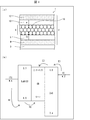
- FIG. 1A is a schematic cross-sectional view of a light emitting device 1 according to this embodiment.
- a light emitting device 1 includes a light emitting element 2 and an array substrate 3.
- the light emitting device 1 has a structure in which each layer of the light emitting element 2 is laminated on an array substrate 3 on which TFTs (Thin Film Transistors) (not shown) are formed.
- TFTs Thin Film Transistors
- the light-emitting element 2 includes a hole transport layer 6, a quantum dot layer 8, an electron transport layer 10, and a second electrode 12 in this order from the lower layer on the first electrode 4.
- the first electrode 4 of the light emitting element 2 formed on the upper layer of the array substrate 3 is electrically connected to the TFT of the array substrate 3.
- the first electrode 4 and the second electrode 12 include a conductive material, and are electrically connected to the hole transport layer 6 and the electron transport layer 10, respectively.
- the first electrode 4 is an anode and the second electrode 12 is a cathode.
- One of the first electrode 4 and the second electrode 12 is a transparent electrode.
- the transparent electrode for example, ITO, IZO, ZnO, AZO, or BZO is used, and the film may be formed by a sputtering method or the like.
- either the 1st electrode 4 or the 2nd electrode 12 may contain the metal material, and as a metal material, Al, Cu, Au, Ag, etc. with a high visible light reflectance are preferable.
- the quantum dot layer 8 is formed by laminating one to several layers of quantum dots (semiconductor nanoparticles) 16.
- the quantum dot layer 8 can be formed from a dispersion liquid in which the quantum dots 16 are dispersed in a solvent such as hexane or toluene by a spin coating method, an inkjet method, or the like.
- a dispersion material such as thiol or amine may be mixed in the dispersion.
- the film thickness of the quantum dot layer 8 is preferably 5 to 50 nm.
- the quantum dot 16 is a light emitting material that has a valence band level and a conduction band level and emits light by recombination of holes in the valence band level and electrons in the conduction band level.
- the light emitted from the quantum dot 16 has a narrow spectrum due to the quantum confinement effect, and therefore, light having a relatively deep chromaticity can be obtained.
- the quantum dots 16 may be, for example, semiconductor nanoparticles having a core / shell structure with CdSe in the core and ZnS in the shell.
- the quantum dots 16 may have CdSe / CdS, InP / ZnS, ZnSe / ZnS, CIGS / ZnS, or the like as a core / shell structure.
- the particle size of the quantum dots 16 is about 3 to 15 nm.
- the wavelength of light emitted from the quantum dot 16 can be controlled by the particle size of the quantum dot 16. For this reason, the wavelength of the light emitted from the light emitting device 1 can be controlled by controlling the particle size of the quantum dots 16.
- the hole transport layer 6 is a layer that transports holes from the first electrode 4 to the quantum dot layer 8.
- the hole transport layer is made of an inorganic material, and has an ionization potential larger than 5.5 eV based on the vacuum level.
- the hole transport layer 6 is made of LaNiO 3 .
- the hole transport layer 6 may be formed by sputtering.
- the thickness of the hole transport layer 6 is preferably 5 to 40 nm.
- the electron transport layer 10 is a layer that transports electrons from the second electrode 12 to the quantum dot layer 8.
- the electron transport layer 10 may have a function of inhibiting hole transport.
- the electron transport layer 10 may contain, for example, ZnO, TiO 2 , Ta 2 O 3 , SrTiO 3 or the like, and may be formed by sputtering.
- the film thickness of the electron transport layer 10 can employ a conventionally known film thickness, and is preferably 10 to 100 nm.
- the hole transport layer and the electron transport layer may be nanoparticles, crystals, polycrystals, or amorphous, respectively.
- FIG. 1B is an energy diagram showing an example of Fermi levels or electron affinity and ionization potential in each layer of the light emitting device 2 according to this embodiment.
- the first electrode 4, the hole transport layer 6, the quantum dot layer 8, the electron transport layer 10, and the second electrode 12 are shown from left to right.
- the Fermi level of each electrode is shown in eV.
- the quantum dot layer 8, and the electron transport layer 10 the ionization potential of each layer based on the vacuum level is shown in units of eV.
- the electron affinity of each layer based on the vacuum level is expressed in units of eV.
- the Fermi level of the first electrode 4 is 4.6 eV
- the Fermi level of the second electrode 12 is 4.3 eV.
- the hole transport layer 6 is made of LaNiO 3 .
- the ionization potential of the hole transport layer 6 is 6.0 eV
- the electron affinity of the hole transport layer 6 is 3.7 eV.
- the case where the electron carrying layer 10 consists of ZnO is shown as an example in FIG.1 (b).
- the ionization potential of the electron transport layer 10 is 7.4 eV
- the electron affinity of the electron transport layer 10 is 4.0 eV.
- the ionization potential in the quantum dot layer 8 is 6 to 7 eV and the electron affinity is 3.5 to 4.0 eV, although it varies depending on the material and particle size of the quantum dots 16.
- the light emission mechanism of the light emitting device 1 according to the present embodiment will be described with reference to FIG.
- holes from the first electrode 4 and electrons from the second electrode 12 are directed toward the quantum dot layer 8. Injected. As indicated by an arrow h + in FIG. 1A, holes from the first electrode 4 reach the quantum dot layer 8 through the hole transport layer 6. As indicated by an arrow e ⁇ in FIG. 1A, electrons from the second electrode 12 reach the quantum dot layer 8 via the electron transport layer 10.
- the holes and electrons that have reached the quantum dot layer 8 recombine at the quantum dots 16 and emit light.
- the light emitted from the quantum dots 16 may be reflected by the second electrode that is a metal electrode, transmitted through the first electrode 4 that is a transparent electrode, and the array substrate 3, and emitted to the outside of the light emitting device 1, for example. .
- the positive electrode 4 is positively transferred from the first electrode 4 to the hole transport layer 6 as indicated by an arrow H ⁇ b> 1 in FIG. Holes are injected. Similarly, electrons are injected from the second electrode 12 into the electron transport layer 10 as indicated by an arrow E1 in FIG.
- the barrier for hole transport from the hole transport layer 6 to the quantum dot layer 8 is indicated by the energy obtained by subtracting the ionization potential of the hole transport layer 6 from the ionization potential of the quantum dot layer 8. Therefore, the hole transport barrier from the hole transport layer 6 to the quantum dot layer 8 in this embodiment is 0 to 1.0 eV.
- FIG. 2 is a schematic cross-sectional view of the light-emitting device 41 according to the comparative example, and an energy diagram showing an example of Fermi level of each layer in the light-emitting element 42 of the light-emitting device 41, or an electron affinity and an ionization potential.
- the light emitting device 41 according to the comparative form is different from the light emitting device 1 according to this embodiment only in that the light emitting device 41 includes a light emitting element 42 including a hole transport layer 46 made of NiO.
- the light emitting device 41 also emits light according to the same principle as in the present embodiment.
- the hole transport barrier from the hole transport layer 46 to the quantum dot layer 8 is 0.5 to 1.5 eV.
- the light-emitting element 2 according to the present embodiment is made of an inorganic material, and includes a hole transport layer 6 having an ionization potential larger than 5.5 eV with respect to the vacuum level. For this reason, according to the light-emitting element 2 according to the present embodiment, as compared with the case where the hole-transporting layer 46 made of NiO is provided as in the light-emitting element 42 according to the comparative example, the quantum dots from the hole-transporting layer 6 The barrier for hole transport to the layer 8 can be reduced. Therefore, the light emitting device 1 according to the present embodiment can improve the light emission efficiency while ensuring the reliability.
- the hole transport layer 6 is made of LaNiO 3 as in the light emitting device 2 according to the present embodiment, CdSe / CdS, InP / ZnS, or ZnSe / ZnS is used as the quantum dot 16 of the quantum dot layer 8.
- the particle size of the quantum dots 16 is preferably 5 to 10 nm.
- the ionization potential of the hole transport layer 6 in this embodiment is preferably larger than the ionization potential of the quantum dot layer 8 or the difference from the ionization potential of the quantum dot layer 8 is 0.5 eV or less. If it is the said structure, the transport barrier from the hole transport layer 6 to the quantum dot layer 8 becomes smaller, and can transport a hole more efficiently from the hole transport layer 6 to the quantum dot layer 8.
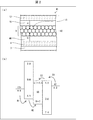
- FIG. 3A is a schematic cross-sectional view of the light emitting device 1 according to this embodiment.
- the light emitting device 1 according to this embodiment is configured only in that an electron blocking layer 18 is provided between the hole transport layer 6 and the quantum dot layer 8 as compared with the light emitting device 1 according to the previous embodiment. Is different.
- the electron blocking layer 18 is a layer having a function of inhibiting leakage of electrons from the quantum dot layer 8 to the hole transport layer 6 side.
- the electron blocking layer 18 may include an inorganic material such as Cu2O, LiNbO3, LiCoO2, Al2O3, SiO2, or SiN, and may include an organic material such as PVK, TFB, or poly-TPD.
- FIG. 3B is an energy diagram showing an example of Fermi levels or electron affinity and ionization potential in each layer of the light emitting device 2 according to this embodiment.
- an electron blocking layer 18 is shown between the hole transport layer 6 and the quantum dot layer 8 as compared with FIG.
- FIG. 3B shows an example in which the electronic block layer 18 is made of PVK.
- the electron block layer 18 in this embodiment has an ionization potential of 5.8 eV and an electron affinity of 2.2 eV.
- the electron block layer 18 has an electron affinity smaller than the electron affinity of the hole transport layer 6 and the quantum dot layer 8.
- the electron blocking layer 18 preferably has an ionization potential smaller than the ionization potential of at least one of the hole transport layer 6 and the quantum dot layer 8.
- the light emitting device 1 when a potential difference is generated between the first electrode 4 and the second electrode 12, holes and electrons are injected as in the previous embodiment.
- the holes transported from the first electrode 4 to the hole transport layer 6 are transported to the quantum dot layer 8 as indicated by an arrow H3.
- the ionization potential of the electron blocking layer 18 is smaller than the ionization potential of the hole transport layer 6 and the quantum dot layer 8, so that the hole transport layer 6 to the quantum dot layer This is because the barrier to hole transport to 8 does not increase.
- the electrons transported from the second electrode 12 to the quantum dot layer 8 via the electron transport layer 10 further move toward the electron block layer 18 as indicated by an arrow E3.
- the electron block layer 18 has an electron affinity smaller than the electron affinity of the quantum dot layer 8
- the barrier for electron injection from the quantum dot layer 8 to the electron block layer 18 is increased. For this reason, injection of electrons transported to the quantum dot layer 8 into the electron block layer 18 is inhibited, and leakage of electrons to the hole transport layer 6 and the first electrode 4 is reduced.
- the light-emitting element 2 in the present embodiment includes an electron block layer 18 that inhibits injection of electrons from the quantum dot layer 8 to the hole transport layer 6. For this reason, in the light emitting device 1 according to this embodiment, it is possible to reduce leakage of electrons transported to the quantum dot layer 8 to the hole transport layer 6 as compared with the light emitting device 1 in the previous embodiment. Therefore, the efficiency of recombination of holes and electrons in the quantum dot layer 8 can be improved, and the light emission efficiency of the light emitting device 1 can be improved.
- the electron affinity of the electron blocking layer 18 is smaller than 3.5 eV, more preferably smaller than 3.0 eV.
- the electron affinity of the electron block layer 18 is 0.5 eV or less smaller than the electron affinity of the quantum dot layer 8. If it is the said structure, the electronic block layer 18 can inhibit the electron leakage mentioned above efficiently.
- the film thickness of the electron block layer 18 is preferably 2 to 40 nm. Furthermore, the electron block layer 18 may be formed of NiO. In this case, the thickness of the electron blocking layer 18 is preferably 2 to 20 nm so that holes transported from the hole transporting layer 6 to the electron blocking layer 18 do not remain in the electron blocking layer 18.
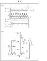
- FIG. 4A is a schematic cross-sectional view of the light emitting device 1 according to this embodiment.
- the light emitting device 1 according to the present embodiment is only in that a hole injection layer 20 is provided between the first electrode 4 and the hole transport layer 6 as compared with the light emitting device 1 according to the first embodiment.
- the configuration is different.
- the hole injection layer 20 is a layer having a function of injecting holes from the first electrode 4 and injecting holes into the hole transport layer 6.
- the hole injection layer 20 may include, for example, NiO, LiNbO 3 , LiCoO 3 , or Cu 2 O.
- FIG. 4B is an energy diagram showing an example of Fermi levels or electron affinity and ionization potential in each layer of the light emitting device 2 according to this embodiment.
- a hole injection layer 20 is shown between the first electrode 4 and the hole transport layer 6 as compared with FIG.
- FIG. 4B shows an example in which the hole injection layer 20 is made of NiO.
- the hole injection layer 20 in this embodiment has an ionization potential of 5.5 eV and an electron affinity of 2.0 eV.
- the hole injection layer 20 has an ionization potential between the Fermi level of the first electrode 4 and the ionization potential of the hole transport layer 6.
- the film thickness of the hole injection layer 20 is preferably 5 to 40 nm.
- the light emitting device 1 when a potential difference is generated between the first electrode 4 and the second electrode 12, holes are injected from the first electrode 4 into the hole injection layer 20 as indicated by an arrow H ⁇ b> 4.
- the barrier for hole injection from the first electrode 4 to the hole injection layer 20 is 0.9 eV.
- the holes injected into the hole injection layer 20 are injected from the hole injection layer 20 into the hole transport layer 6 as indicated by an arrow H5.
- the barrier for hole injection from the hole injection layer 20 to the hole transport layer 6 is 0.5 eV. Subsequent hole transport and electrons may be transported as in the first embodiment.
- holes are transported from the first electrode 4 to the hole transport layer 6 through the hole injection layer 20.
- the hole injection from the first electrode 4 is higher than the hole injection barrier from the first electrode 4 to the hole transport layer 6.
- the barrier for hole injection into the layer 20 or the hole injection from the hole injection layer 20 to the hole transport layer 6 is small. Therefore, holes can be efficiently transported from the first electrode 4 to the hole transport layer 6.
- holes can be more efficiently injected into the quantum dot layer 8 than the light emitting device 1 in the previous embodiment, and the light emission efficiency of the light emitting device 1 can be improved. Can be improved.
- FIG. 5 is a schematic cross-sectional view of a light-emitting device 1 according to a modification of the present embodiment, and an energy diagram showing an example of Fermi levels of each layer or electron affinity and ionization potential in the light-emitting element 2 of the light-emitting device 1. .
- the light emitting device 1 according to this modification is configured only in that an electron blocking layer 18 is provided between the hole transport layer 6 and the quantum dot layer 8 as compared with the light emitting device 1 according to this embodiment. Is different.
- the hole transport layer 6 is transferred from the first electrode 4 through the hole injection layer 20. Holes are injected. Next, holes are transported from the hole transport layer 6 to the quantum dot layer 8 in the same manner as the light emitting device 2 according to the second embodiment. In the transport of electrons in the light emitting device 2 according to this modification, electrons are transported from the second electrode 12 to the quantum dot layer 8 through the electron transport layer 10 as in the light emitting device 2 according to the second embodiment. The electrons transported to the quantum dot layer 8 are inhibited from being injected into the hole transport layer 6 by the electron block layer 18.
- the light emitting device 1 according to the present modification like the light emitting device 1 according to the present embodiment, maintains the efficiency of transporting holes to the quantum dot layer 8 while maintaining the efficiency from the quantum dot layer 8 to the hole transport layer 6. Blocks electron injection. Therefore, the efficiency of recombination of holes and electrons in the quantum dot layer 8 is further improved, and the light emission efficiency of the light emitting device 1 can be further improved.
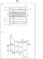
- FIG. 6A is a schematic cross-sectional view of the light emitting device 1 according to this embodiment.
- the light emitting device 1 according to the present embodiment is different from the light emitting device 1 according to the third embodiment only in that a hole injection layer 22 is provided instead of the hole injection layer 20.
- the hole injection layer 22 is made of NiO and LaNiO 3 .
- the NiO density gradually decreases and the LaNiO 3 density gradually increases from the end face on the first electrode 4 side to the end face on the hole transport layer 6 side. That is, the hole injection layer 22 is made of NiO at the end face in contact with the first electrode 4, and NiO is gradually replaced with LaNiO 3 toward the hole transport layer 6, and the end face in contact with the hole transport layer 6 is made of LaNiO 3.
- the thickness of the hole injection layer 22 is preferably 5 to 40 nm.
- the hole injection layer 22 can be manufactured by simultaneously sputtering NiO and LaO.
- NiO and LaO may be sputtered simultaneously by keeping the power of the sputtering apparatus for depositing NiO constant and gradually increasing the power of the sputtering apparatus for depositing LaO.
- FIG. 6B is an energy diagram showing an example of Fermi levels or electron affinity and ionization potential in each layer of the light emitting device 2 according to this embodiment.
- a hole injection layer 22 is shown instead of the hole injection layer 20, as compared with FIG.
- the composition of the hole injection layer 22 in this embodiment is changed from NiO to LaNiO 3 from the end face on the first electrode 4 side to the end face on the hole transport layer 6 side. Reflecting this, as shown in FIG. 6B, the apparent ionization potential of the hole injection layer 22 is 5.5 eV to 6.0 eV from the first electrode 4 to the hole transport layer 6. Has increased. Also, as shown in FIG. 6B, the apparent electron affinity of the hole injection layer 22 also increases from 2.0 eV to 3.7 eV from the first electrode 4 to the hole transport layer 6. Yes.
- the light emitting device 1 when a potential difference is generated between the first electrode 4 and the second electrode 12, holes are injected from the first electrode 4 into the hole injection layer 22 as indicated by an arrow H4. Next, the holes injected into the hole injection layer 22 are transported through the hole injection layer 22 from the first electrode 4 toward the hole transport layer 6 as indicated by an arrow H6.
- the hole transport barrier in the hole injection layer 22 is small. Further, since the ionization potential between the end surface of the hole injection layer 22 on the hole transport layer 6 side and the hole transport layer 6 does not substantially change, a barrier for hole injection from the hole injection layer 22 to the hole transport layer 6 is achieved. Is very small.
- holes are injected from the first electrode 4 into the hole transport layer 6 through the hole injection layer 22. Subsequent hole transport and electrons may be transported as in the first embodiment.
- holes are transported from the first electrode 4 to the hole transport layer 6 through the hole injection layer 22. For this reason, the injection of holes from the hole injection layer 22 to the hole transport layer 6 is performed more efficiently. Therefore, in the light emitting device 1 according to the present embodiment, holes can be more efficiently transported to the quantum dot layer 8 than the light emitting device 1 in the previous embodiment, and the light emission efficiency of the light emitting device 1 can be improved. Can be improved.
- FIG. 7 is a schematic cross-sectional view of a light-emitting device 1 according to a modification of the present embodiment, and an energy diagram showing an example of Fermi levels of each layer or electron affinity and ionization potential in the light-emitting element 2 of the light-emitting device 1. .
- the light emitting device 1 according to this modification is configured only in that an electron blocking layer 18 is provided between the hole transport layer 6 and the quantum dot layer 8 as compared with the light emitting device 1 according to this embodiment. Is different.
- the hole transport layer 6 is transferred from the first electrode 4 through the hole injection layer 22. Holes are injected. Next, holes are transported from the hole transport layer 6 to the quantum dot layer 8 in the same manner as the light emitting device 2 according to the second embodiment. In the transport of electrons in the light emitting device 2 according to this modification, electrons are injected from the second electrode 12 into the quantum dot layer 8 through the electron transport layer 10 as in the light emitting device 2 according to the second embodiment. The electrons injected into the quantum dot layer 8 are inhibited from being injected into the hole transport layer 6 by the electron block layer 18.
- the light emitting device 1 according to the present modification like the light emitting device 1 according to the present embodiment, maintains the efficiency of transporting holes to the quantum dot layer 8 while maintaining the efficiency from the quantum dot layer 8 to the hole transport layer 6. Blocks electron injection. Therefore, the efficiency of recombination of holes and electrons in the quantum dot layer 8 is further improved, and the light emission efficiency of the light emitting device 1 can be further improved.
- each of the above-described embodiments a structure including the light emitting element 2 including the first electrode, the hole transport layer, the quantum dot layer, the electron transport layer, and the second electrode in order from the lower layer on the array substrate 3.
- the light emitting device 1 having the above has been described as an example.
- each of the embodiments described above includes the second electrode, the electron transport layer, the quantum dot layer, the hole transport layer, and the first electrode on the array substrate 3 in the reverse order, that is, in order from the lower layer.
- the present invention can also be applied to a light emitting device 1 having a structure including the light emitting element 2.
- FIG. 8 is a block diagram showing the light emitting element manufacturing apparatus 30 according to each of the embodiments described above.
- the light emitting element manufacturing apparatus 30 may include a controller 32 and a film forming apparatus 34.
- the controller 32 may control the film forming apparatus 34.
- the film forming apparatus 34 may form each layer of the light emitting element 2.
- the light-emitting element according to aspect 1 includes a first electrode, a second electrode, a quantum dot layer between which the quantum dots are stacked, between the first electrode and the second electrode, and between the quantum dot layer and the first electrode. And a hole transport layer made of LaNiO 3 .
- the light-emitting element according to aspect 2 includes a first electrode, a second electrode, a quantum dot layer in which quantum dots are stacked between the first electrode and the second electrode, and between the quantum dot layer and the first electrode. And a hole transport layer having an ionization potential larger than 5.5 eV based on the vacuum level.
- the ionization potential of the hole transport layer is greater than the ionization potential of the quantum dot layer, or the difference in ionization potential between the quantum dot layer and the hole transport layer is 0.5 eV or less. is there.
- an electron block layer is provided between the quantum dot layer and the hole transport layer, and the electron affinity of the electron block layer is smaller than the electron affinity of the hole transport layer.
- the electron affinity of the electron block layer is 0.5 eV or less smaller than the electron affinity of the quantum dot layer.
- the electron affinity of the electron block layer is smaller than 3.5 eV with respect to the vacuum level.
- a hole injection layer is provided between the first electrode and the hole transport layer, and the ionization potential of the hole injection layer is such that the Fermi level of the first electrode and the hole transport are Between the ionization potential of the layers.
- the hole injection layer is made of NiO and LaNiO 3, and in the hole injection layer, the density of NiO gradually decreases from the end surface on the first electrode side to the end surface on the hole transport layer side. However, the density of LaNiO 3 gradually increases.
- the light-emitting device includes the light-emitting element according to any of the above-described aspects.
- the light emitting element manufacturing apparatus includes a first electrode, a second electrode, a quantum dot layer in which quantum dots between the first electrode and the second electrode are stacked, the quantum dot layer, and the first electrode. And a hole transport layer made of LaNiO 3 .
- the light emitting device manufacturing apparatus includes a first electrode, a second electrode, a quantum dot layer in which quantum dots between the first electrode and the second electrode are stacked, the quantum dot layer, and the first electrode. And a hole transport layer which is made of an inorganic material and has an ionization potential larger than 5.5 eV with respect to the vacuum level.
Landscapes
- Physics & Mathematics (AREA)
- Optics & Photonics (AREA)
- Engineering & Computer Science (AREA)
- Manufacturing & Machinery (AREA)
- Chemical & Material Sciences (AREA)
- Crystallography & Structural Chemistry (AREA)
- Inorganic Chemistry (AREA)
- Nanotechnology (AREA)
- Electroluminescent Light Sources (AREA)
Abstract
Dans le but d'améliorer l'efficacité d'injection de trous d'une couche de transport de trous à une couche de points quantiques, l'invention concerne un élément électroluminescent (2) comprenant : une première électrode (4) ; une seconde électrode (12) ; une couche de points quantiques (8) qui est disposée entre la première électrode (4) et la seconde électrode (12), et dans laquelle des points quantiques (16) sont disposés en couches ; et une couche de transport de trous (6) disposée entre la couche de points quantiques (8) et la première électrode (4), qui est soit une couche de transport de trous (6) formée à partir de LaNiO3, soit une couche de transport de trous (6) formée à partir d'un matériau inorganique et qui a un potentiel d'ionisation supérieur à 5,5 eV par rapport au niveau de vide.
Priority Applications (2)
| Application Number | Priority Date | Filing Date | Title |
|---|---|---|---|
| PCT/JP2018/004915 WO2019159236A1 (fr) | 2018-02-13 | 2018-02-13 | Élément électroluminescent, dispositif électroluminescent et dispositif de production d'élément électroluminescent |
| US16/968,059 US11417851B2 (en) | 2018-02-13 | 2018-02-13 | Light-emitting element, light-emitting device, and device for producing light-emitting element |
Applications Claiming Priority (1)
| Application Number | Priority Date | Filing Date | Title |
|---|---|---|---|
| PCT/JP2018/004915 WO2019159236A1 (fr) | 2018-02-13 | 2018-02-13 | Élément électroluminescent, dispositif électroluminescent et dispositif de production d'élément électroluminescent |
Publications (1)
| Publication Number | Publication Date |
|---|---|
| WO2019159236A1 true WO2019159236A1 (fr) | 2019-08-22 |
Family
ID=67620999
Family Applications (1)
| Application Number | Title | Priority Date | Filing Date |
|---|---|---|---|
| PCT/JP2018/004915 WO2019159236A1 (fr) | 2018-02-13 | 2018-02-13 | Élément électroluminescent, dispositif électroluminescent et dispositif de production d'élément électroluminescent |
Country Status (2)
| Country | Link |
|---|---|
| US (1) | US11417851B2 (fr) |
| WO (1) | WO2019159236A1 (fr) |
Cited By (2)
| Publication number | Priority date | Publication date | Assignee | Title |
|---|---|---|---|---|
| CN113206198A (zh) * | 2021-04-19 | 2021-08-03 | 武汉大学 | 一种镍酸镧纳米颗粒空穴传输层的制备方法、反式钙钛矿太阳能电池及其制备方法 |
| US20220149249A1 (en) * | 2019-02-20 | 2022-05-12 | Sharp Kabushiki Kaisha | Method for manufacturing light-emitting device |
Families Citing this family (2)
| Publication number | Priority date | Publication date | Assignee | Title |
|---|---|---|---|---|
| WO2020170370A1 (fr) * | 2019-02-20 | 2020-08-27 | シャープ株式会社 | Procédé de fabrication de dispositif électroluminescent |
| US20220158108A1 (en) * | 2019-02-27 | 2022-05-19 | Sharp Kabushiki Kaisha | Light-emitting element and display device using light-emitting element |
Citations (7)
| Publication number | Priority date | Publication date | Assignee | Title |
|---|---|---|---|---|
| JP2006073685A (ja) * | 2004-08-31 | 2006-03-16 | Tdk Corp | 積層体ユニットおよび薄膜容量素子 |
| JP2013201001A (ja) * | 2012-03-23 | 2013-10-03 | Nippon Shokubai Co Ltd | 積層体並びに該積層体を用いた有機エレクトロルミネッセンス素子、発光ダイオード素子及び光電変換素子 |
| JP2015092494A (ja) * | 2014-12-24 | 2015-05-14 | ユー・ディー・シー アイルランド リミテッド | 有機電界発光素子及びその製造方法 |
| JP2016197601A (ja) * | 2010-07-26 | 2016-11-24 | メルク パテント ゲーエムベーハー | 量子ドットおよびホスト |
| JP2017143279A (ja) * | 2012-02-17 | 2017-08-17 | 株式会社半導体エネルギー研究所 | 光電変換装置 |
| JP2017168420A (ja) * | 2015-09-01 | 2017-09-21 | 株式会社半導体エネルギー研究所 | 発光素子、発光装置、電子機器及び照明装置 |
| JP2017188186A (ja) * | 2014-08-26 | 2017-10-12 | パナソニックIpマネジメント株式会社 | 有機エレクトロルミネッセンス素子 |
Family Cites Families (1)
| Publication number | Priority date | Publication date | Assignee | Title |
|---|---|---|---|---|
| KR20130007649A (ko) | 2005-02-16 | 2013-01-18 | 매사추세츠 인스티튜트 오브 테크놀로지 | 반도체 나노결정을 포함하는 발광 디바이스 |
-
2018
- 2018-02-13 WO PCT/JP2018/004915 patent/WO2019159236A1/fr active Application Filing
- 2018-02-13 US US16/968,059 patent/US11417851B2/en active Active
Patent Citations (7)
| Publication number | Priority date | Publication date | Assignee | Title |
|---|---|---|---|---|
| JP2006073685A (ja) * | 2004-08-31 | 2006-03-16 | Tdk Corp | 積層体ユニットおよび薄膜容量素子 |
| JP2016197601A (ja) * | 2010-07-26 | 2016-11-24 | メルク パテント ゲーエムベーハー | 量子ドットおよびホスト |
| JP2017143279A (ja) * | 2012-02-17 | 2017-08-17 | 株式会社半導体エネルギー研究所 | 光電変換装置 |
| JP2013201001A (ja) * | 2012-03-23 | 2013-10-03 | Nippon Shokubai Co Ltd | 積層体並びに該積層体を用いた有機エレクトロルミネッセンス素子、発光ダイオード素子及び光電変換素子 |
| JP2017188186A (ja) * | 2014-08-26 | 2017-10-12 | パナソニックIpマネジメント株式会社 | 有機エレクトロルミネッセンス素子 |
| JP2015092494A (ja) * | 2014-12-24 | 2015-05-14 | ユー・ディー・シー アイルランド リミテッド | 有機電界発光素子及びその製造方法 |
| JP2017168420A (ja) * | 2015-09-01 | 2017-09-21 | 株式会社半導体エネルギー研究所 | 発光素子、発光装置、電子機器及び照明装置 |
Cited By (2)
| Publication number | Priority date | Publication date | Assignee | Title |
|---|---|---|---|---|
| US20220149249A1 (en) * | 2019-02-20 | 2022-05-12 | Sharp Kabushiki Kaisha | Method for manufacturing light-emitting device |
| CN113206198A (zh) * | 2021-04-19 | 2021-08-03 | 武汉大学 | 一种镍酸镧纳米颗粒空穴传输层的制备方法、反式钙钛矿太阳能电池及其制备方法 |
Also Published As
| Publication number | Publication date |
|---|---|
| US11417851B2 (en) | 2022-08-16 |
| US20210057662A1 (en) | 2021-02-25 |
Similar Documents
| Publication | Publication Date | Title |
|---|---|---|
| WO2019159236A1 (fr) | Élément électroluminescent, dispositif électroluminescent et dispositif de production d'élément électroluminescent | |
| US11342527B2 (en) | Light-emitting element having commonly formed hole transport layer and anode electrode and light-emitting device | |
| WO2019187064A1 (fr) | Élément électroluminescent, dispositif électroluminescent et procédé de production d'un élément électroluminescent | |
| CN112186124B (zh) | 有机发光二极管和显示面板 | |
| WO2021100104A1 (fr) | Élément et dispositif électroluminescents | |
| KR102607857B1 (ko) | 코어쉘 구조의 나노 입자를 포함하는 발광 소자 | |
| WO2020208810A1 (fr) | Élément électroluminescent , dispositif d'affichage, et procédé de production d'un élément électroluminescent | |
| DE102014102565B4 (de) | Optoelektronisches Bauelement und Verfahren zum Herstellen eines optoelektronischen Bauelements | |
| WO2019165716A1 (fr) | Dispositif d'émission de lumière et son procédé de fabrication, et dispositif d'affichage | |
| WO2020134163A1 (fr) | Diode électroluminescente à points quantiques et son procédé de préparation | |
| WO2021059452A1 (fr) | Élément électroluminescent et dispositif électroluminescent | |
| WO2021033257A1 (fr) | Élément et dispositif électroluminescents | |
| CN209912898U (zh) | 量子点发光二极管 | |
| WO2020261347A1 (fr) | Élément électroluminescent | |
| WO2019159216A1 (fr) | Dispositif électroluminescent | |
| WO2022079817A1 (fr) | Élément électroluminescent | |
| US20230041812A1 (en) | Light-emitting element and display device | |
| WO2021214910A1 (fr) | Élément électroluminescent et dispositif d'affichage | |
| WO2021053787A1 (fr) | Élément électroluminescent et dispositif d'affichage | |
| WO2021059472A1 (fr) | Dispositif d'éclairage | |
| KR101961355B1 (ko) | 유기발광장치 | |
| WO2022252052A1 (fr) | Diode électroluminescente à points quantiques et son procédé de fabrication, et dispositif d'affichage | |
| US20230284469A1 (en) | Light-emitting element, and light-emitting device | |
| WO2022059204A1 (fr) | Élément électroluminescent | |
| WO2022029856A1 (fr) | Élément électroluminescent et dispositif électroluminescent |
Legal Events
| Date | Code | Title | Description |
|---|---|---|---|
| 121 | Ep: the epo has been informed by wipo that ep was designated in this application |
Ref document number: 18906475 Country of ref document: EP Kind code of ref document: A1 |
|
| NENP | Non-entry into the national phase |
Ref country code: DE |
|
| 122 | Ep: pct application non-entry in european phase |
Ref document number: 18906475 Country of ref document: EP Kind code of ref document: A1 |
|
| NENP | Non-entry into the national phase |
Ref country code: JP |