WO2019159236A1 - Light-emitting element, light-emitting device, and device for producing light-emitting element - Google Patents
Light-emitting element, light-emitting device, and device for producing light-emitting element Download PDFInfo
- Publication number
- WO2019159236A1 WO2019159236A1 PCT/JP2018/004915 JP2018004915W WO2019159236A1 WO 2019159236 A1 WO2019159236 A1 WO 2019159236A1 JP 2018004915 W JP2018004915 W JP 2018004915W WO 2019159236 A1 WO2019159236 A1 WO 2019159236A1
- Authority
- WO
- WIPO (PCT)
- Prior art keywords
- layer
- electrode
- quantum dot
- hole transport
- light emitting
- Prior art date
Links
- 239000002096 quantum dot Substances 0.000 claims abstract description 138
- 230000005525 hole transport Effects 0.000 claims abstract description 127
- 238000002347 injection Methods 0.000 claims abstract description 64
- 239000007924 injection Substances 0.000 claims abstract description 64
- 229910010272 inorganic material Inorganic materials 0.000 claims abstract description 15
- 239000011147 inorganic material Substances 0.000 claims abstract description 15
- 241000877463 Lanio Species 0.000 claims description 18
- 230000000903 blocking effect Effects 0.000 claims description 13
- 238000004519 manufacturing process Methods 0.000 claims description 11
- 230000007423 decrease Effects 0.000 claims description 4
- 229910002340 LaNiO3 Inorganic materials 0.000 abstract 1
- 230000032258 transport Effects 0.000 description 29
- 238000010586 diagram Methods 0.000 description 16
- 230000004888 barrier function Effects 0.000 description 13
- 230000004048 modification Effects 0.000 description 13
- 238000012986 modification Methods 0.000 description 13
- 239000010408 film Substances 0.000 description 11
- 239000000758 substrate Substances 0.000 description 9
- 238000004544 sputter deposition Methods 0.000 description 6
- 239000002245 particle Substances 0.000 description 5
- 238000005215 recombination Methods 0.000 description 4
- 230000006798 recombination Effects 0.000 description 4
- YXFVVABEGXRONW-UHFFFAOYSA-N Toluene Chemical compound CC1=CC=CC=C1 YXFVVABEGXRONW-UHFFFAOYSA-N 0.000 description 3
- UHYPYGJEEGLRJD-UHFFFAOYSA-N cadmium(2+);selenium(2-) Chemical compound [Se-2].[Cd+2] UHYPYGJEEGLRJD-UHFFFAOYSA-N 0.000 description 3
- 230000000052 comparative effect Effects 0.000 description 3
- 239000006185 dispersion Substances 0.000 description 3
- 239000000463 material Substances 0.000 description 3
- VLKZOEOYAKHREP-UHFFFAOYSA-N n-Hexane Chemical compound CCCCCC VLKZOEOYAKHREP-UHFFFAOYSA-N 0.000 description 3
- 239000002105 nanoparticle Substances 0.000 description 3
- VYPSYNLAJGMNEJ-UHFFFAOYSA-N Silicium dioxide Chemical compound O=[Si]=O VYPSYNLAJGMNEJ-UHFFFAOYSA-N 0.000 description 2
- 238000000151 deposition Methods 0.000 description 2
- 230000002401 inhibitory effect Effects 0.000 description 2
- 239000007769 metal material Substances 0.000 description 2
- 238000000034 method Methods 0.000 description 2
- 239000011368 organic material Substances 0.000 description 2
- SBIBMFFZSBJNJF-UHFFFAOYSA-N selenium;zinc Chemical compound [Se]=[Zn] SBIBMFFZSBJNJF-UHFFFAOYSA-N 0.000 description 2
- 239000004065 semiconductor Substances 0.000 description 2
- 229910012820 LiCoO Inorganic materials 0.000 description 1
- 229910032387 LiCoO2 Inorganic materials 0.000 description 1
- 229910013641 LiNbO 3 Inorganic materials 0.000 description 1
- 229910003327 LiNbO3 Inorganic materials 0.000 description 1
- 229910004541 SiN Inorganic materials 0.000 description 1
- 229910002367 SrTiO Inorganic materials 0.000 description 1
- -1 Ta 2 O 3 Inorganic materials 0.000 description 1
- 229910010413 TiO 2 Inorganic materials 0.000 description 1
- 229910052782 aluminium Inorganic materials 0.000 description 1
- PNEYBMLMFCGWSK-UHFFFAOYSA-N aluminium oxide Inorganic materials [O-2].[O-2].[O-2].[Al+3].[Al+3] PNEYBMLMFCGWSK-UHFFFAOYSA-N 0.000 description 1
- 150000001412 amines Chemical class 0.000 description 1
- QVGXLLKOCUKJST-UHFFFAOYSA-N atomic oxygen Chemical compound [O] QVGXLLKOCUKJST-UHFFFAOYSA-N 0.000 description 1
- 230000008859 change Effects 0.000 description 1
- 229910052681 coesite Inorganic materials 0.000 description 1
- 239000004020 conductor Substances 0.000 description 1
- 229910052802 copper Inorganic materials 0.000 description 1
- BERDEBHAJNAUOM-UHFFFAOYSA-N copper(I) oxide Inorganic materials [Cu]O[Cu] BERDEBHAJNAUOM-UHFFFAOYSA-N 0.000 description 1
- 229910052593 corundum Inorganic materials 0.000 description 1
- 229910052906 cristobalite Inorganic materials 0.000 description 1
- 239000013078 crystal Substances 0.000 description 1
- KRFJLUBVMFXRPN-UHFFFAOYSA-N cuprous oxide Chemical compound [O-2].[Cu+].[Cu+] KRFJLUBVMFXRPN-UHFFFAOYSA-N 0.000 description 1
- 230000000694 effects Effects 0.000 description 1
- 229910052737 gold Inorganic materials 0.000 description 1
- 238000010030 laminating Methods 0.000 description 1
- 239000007788 liquid Substances 0.000 description 1
- 230000007246 mechanism Effects 0.000 description 1
- 239000002184 metal Substances 0.000 description 1
- 229910052751 metal Inorganic materials 0.000 description 1
- 239000000203 mixture Substances 0.000 description 1
- GNRSAWUEBMWBQH-UHFFFAOYSA-N nickel(II) oxide Inorganic materials [Ni]=O GNRSAWUEBMWBQH-UHFFFAOYSA-N 0.000 description 1
- 229910052760 oxygen Inorganic materials 0.000 description 1
- 239000001301 oxygen Substances 0.000 description 1
- 239000004054 semiconductor nanocrystal Substances 0.000 description 1
- 239000000377 silicon dioxide Substances 0.000 description 1
- 235000012239 silicon dioxide Nutrition 0.000 description 1
- 229910052709 silver Inorganic materials 0.000 description 1
- 239000002904 solvent Substances 0.000 description 1
- 238000001228 spectrum Methods 0.000 description 1
- 238000004528 spin coating Methods 0.000 description 1
- 229910052682 stishovite Inorganic materials 0.000 description 1
- 239000010409 thin film Substances 0.000 description 1
- 150000003573 thiols Chemical class 0.000 description 1
- 229910052905 tridymite Inorganic materials 0.000 description 1
- 229910001845 yogo sapphire Inorganic materials 0.000 description 1
Images


Classifications
-
- H—ELECTRICITY
- H10—SEMICONDUCTOR DEVICES; ELECTRIC SOLID-STATE DEVICES NOT OTHERWISE PROVIDED FOR
- H10K—ORGANIC ELECTRIC SOLID-STATE DEVICES
- H10K50/00—Organic light-emitting devices
- H10K50/10—OLEDs or polymer light-emitting diodes [PLED]
- H10K50/11—OLEDs or polymer light-emitting diodes [PLED] characterised by the electroluminescent [EL] layers
- H10K50/115—OLEDs or polymer light-emitting diodes [PLED] characterised by the electroluminescent [EL] layers comprising active inorganic nanostructures, e.g. luminescent quantum dots
-
- H—ELECTRICITY
- H05—ELECTRIC TECHNIQUES NOT OTHERWISE PROVIDED FOR
- H05B—ELECTRIC HEATING; ELECTRIC LIGHT SOURCES NOT OTHERWISE PROVIDED FOR; CIRCUIT ARRANGEMENTS FOR ELECTRIC LIGHT SOURCES, IN GENERAL
- H05B33/00—Electroluminescent light sources
- H05B33/10—Apparatus or processes specially adapted to the manufacture of electroluminescent light sources
-
- H—ELECTRICITY
- H05—ELECTRIC TECHNIQUES NOT OTHERWISE PROVIDED FOR
- H05B—ELECTRIC HEATING; ELECTRIC LIGHT SOURCES NOT OTHERWISE PROVIDED FOR; CIRCUIT ARRANGEMENTS FOR ELECTRIC LIGHT SOURCES, IN GENERAL
- H05B33/00—Electroluminescent light sources
- H05B33/12—Light sources with substantially two-dimensional radiating surfaces
- H05B33/14—Light sources with substantially two-dimensional radiating surfaces characterised by the chemical or physical composition or the arrangement of the electroluminescent material, or by the simultaneous addition of the electroluminescent material in or onto the light source
-
- H—ELECTRICITY
- H10—SEMICONDUCTOR DEVICES; ELECTRIC SOLID-STATE DEVICES NOT OTHERWISE PROVIDED FOR
- H10K—ORGANIC ELECTRIC SOLID-STATE DEVICES
- H10K50/00—Organic light-emitting devices
- H10K50/10—OLEDs or polymer light-emitting diodes [PLED]
- H10K50/14—Carrier transporting layers
- H10K50/15—Hole transporting layers
-
- H—ELECTRICITY
- H10—SEMICONDUCTOR DEVICES; ELECTRIC SOLID-STATE DEVICES NOT OTHERWISE PROVIDED FOR
- H10K—ORGANIC ELECTRIC SOLID-STATE DEVICES
- H10K50/00—Organic light-emitting devices
- H10K50/10—OLEDs or polymer light-emitting diodes [PLED]
- H10K50/17—Carrier injection layers
-
- H—ELECTRICITY
- H10—SEMICONDUCTOR DEVICES; ELECTRIC SOLID-STATE DEVICES NOT OTHERWISE PROVIDED FOR
- H10K—ORGANIC ELECTRIC SOLID-STATE DEVICES
- H10K71/00—Manufacture or treatment specially adapted for the organic devices covered by this subclass
Definitions
- the present invention relates to a light emitting element including quantum dots, a light emitting device including the light emitting element, and a light emitting element manufacturing apparatus.
- Patent Document 1 discloses a light emitting device including a semiconductor nanocrystal.
- the light emitting device of Patent Document 1 includes a light emitting element including a hole transport layer made of NiO that is an inorganic material.
- a light emitting device including a light emitting element including a hole transport layer made of an inorganic material has oxygen, moisture, and ultraviolet light as compared with a light emitting device including a light emitting element including a hole transport layer made of an organic material. It is preferable from the viewpoint of improving the reliability of the light emitting device.
- Japanese Patent Publication Japanese Patent Laid-Open No. 2012-23388 (Released on February 2, 2012)”
- the ionization potential of quantum dots is 6 to 7 eV based on the vacuum level.
- the ionization potential of NiO, which is an inorganic material, is 5.5 eV. For this reason, the difference in ionization potential between NiO and quantum dots is as large as 0.5 to 1.5 eV.
- the efficiency of hole transport from the hole transport layer to the quantum dot layer is poor. Therefore, in a light emitting device employing a conventional inorganic material for the hole transport layer, the hole transport efficiency from the hole transport layer to the quantum dot layer and the electron transport efficiency from the electron transport layer to the quantum dot layer are This leads to a decrease in the light emission efficiency of the light emitting element.
- a light-emitting element of the present invention includes a first electrode, a second electrode, a quantum dot layer in which quantum dots are stacked between the first electrode and the second electrode, and the quantum dot layer. And a hole transport layer made of LaNiO 3 between the first electrode and the first electrode.
- a light-emitting element of the present invention includes a first electrode, a second electrode, a quantum dot layer in which quantum dots are stacked between the first electrode and the second electrode, and the quantum A hole transport layer made of an inorganic material between the dot layer and the first electrode and having an ionization potential larger than 5.5 eV with respect to the vacuum level is provided.
- a light emitting device manufacturing apparatus includes a first electrode, a second electrode, a quantum dot layer in which quantum dots are stacked between the first electrode and the second electrode, and And a film forming apparatus for forming a hole transport layer made of LaNiO 3 between the quantum dot layer and the first electrode.
- a light emitting device manufacturing apparatus includes a first electrode, a second electrode, a quantum dot layer in which quantum dots are stacked between the first electrode and the second electrode, and And a film forming apparatus for forming a hole transport layer made of an inorganic material and having an ionization potential larger than 5.5 eV based on a vacuum level, between the quantum dot layer and the first electrode.
- the hole transport efficiency from the hole transport layer to the quantum dot layer is improved.
- the balance of the transport efficiency of holes and electrons to the quantum dot layer is improved, it is possible to provide a light emitting device in which the light emission efficiency of the light emitting element is improved while maintaining the reliability of the light emitting element.
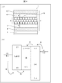
- FIG. 1A is a schematic cross-sectional view of a light emitting device 1 according to this embodiment.
- a light emitting device 1 includes a light emitting element 2 and an array substrate 3.
- the light emitting device 1 has a structure in which each layer of the light emitting element 2 is laminated on an array substrate 3 on which TFTs (Thin Film Transistors) (not shown) are formed.
- TFTs Thin Film Transistors
- the light-emitting element 2 includes a hole transport layer 6, a quantum dot layer 8, an electron transport layer 10, and a second electrode 12 in this order from the lower layer on the first electrode 4.
- the first electrode 4 of the light emitting element 2 formed on the upper layer of the array substrate 3 is electrically connected to the TFT of the array substrate 3.
- the first electrode 4 and the second electrode 12 include a conductive material, and are electrically connected to the hole transport layer 6 and the electron transport layer 10, respectively.
- the first electrode 4 is an anode and the second electrode 12 is a cathode.
- One of the first electrode 4 and the second electrode 12 is a transparent electrode.
- the transparent electrode for example, ITO, IZO, ZnO, AZO, or BZO is used, and the film may be formed by a sputtering method or the like.
- either the 1st electrode 4 or the 2nd electrode 12 may contain the metal material, and as a metal material, Al, Cu, Au, Ag, etc. with a high visible light reflectance are preferable.
- the quantum dot layer 8 is formed by laminating one to several layers of quantum dots (semiconductor nanoparticles) 16.
- the quantum dot layer 8 can be formed from a dispersion liquid in which the quantum dots 16 are dispersed in a solvent such as hexane or toluene by a spin coating method, an inkjet method, or the like.
- a dispersion material such as thiol or amine may be mixed in the dispersion.
- the film thickness of the quantum dot layer 8 is preferably 5 to 50 nm.
- the quantum dot 16 is a light emitting material that has a valence band level and a conduction band level and emits light by recombination of holes in the valence band level and electrons in the conduction band level.
- the light emitted from the quantum dot 16 has a narrow spectrum due to the quantum confinement effect, and therefore, light having a relatively deep chromaticity can be obtained.
- the quantum dots 16 may be, for example, semiconductor nanoparticles having a core / shell structure with CdSe in the core and ZnS in the shell.
- the quantum dots 16 may have CdSe / CdS, InP / ZnS, ZnSe / ZnS, CIGS / ZnS, or the like as a core / shell structure.
- the particle size of the quantum dots 16 is about 3 to 15 nm.
- the wavelength of light emitted from the quantum dot 16 can be controlled by the particle size of the quantum dot 16. For this reason, the wavelength of the light emitted from the light emitting device 1 can be controlled by controlling the particle size of the quantum dots 16.
- the hole transport layer 6 is a layer that transports holes from the first electrode 4 to the quantum dot layer 8.
- the hole transport layer is made of an inorganic material, and has an ionization potential larger than 5.5 eV based on the vacuum level.
- the hole transport layer 6 is made of LaNiO 3 .
- the hole transport layer 6 may be formed by sputtering.
- the thickness of the hole transport layer 6 is preferably 5 to 40 nm.
- the electron transport layer 10 is a layer that transports electrons from the second electrode 12 to the quantum dot layer 8.
- the electron transport layer 10 may have a function of inhibiting hole transport.
- the electron transport layer 10 may contain, for example, ZnO, TiO 2 , Ta 2 O 3 , SrTiO 3 or the like, and may be formed by sputtering.
- the film thickness of the electron transport layer 10 can employ a conventionally known film thickness, and is preferably 10 to 100 nm.
- the hole transport layer and the electron transport layer may be nanoparticles, crystals, polycrystals, or amorphous, respectively.
- FIG. 1B is an energy diagram showing an example of Fermi levels or electron affinity and ionization potential in each layer of the light emitting device 2 according to this embodiment.
- the first electrode 4, the hole transport layer 6, the quantum dot layer 8, the electron transport layer 10, and the second electrode 12 are shown from left to right.
- the Fermi level of each electrode is shown in eV.
- the quantum dot layer 8, and the electron transport layer 10 the ionization potential of each layer based on the vacuum level is shown in units of eV.
- the electron affinity of each layer based on the vacuum level is expressed in units of eV.
- the Fermi level of the first electrode 4 is 4.6 eV
- the Fermi level of the second electrode 12 is 4.3 eV.
- the hole transport layer 6 is made of LaNiO 3 .
- the ionization potential of the hole transport layer 6 is 6.0 eV
- the electron affinity of the hole transport layer 6 is 3.7 eV.
- the case where the electron carrying layer 10 consists of ZnO is shown as an example in FIG.1 (b).
- the ionization potential of the electron transport layer 10 is 7.4 eV
- the electron affinity of the electron transport layer 10 is 4.0 eV.
- the ionization potential in the quantum dot layer 8 is 6 to 7 eV and the electron affinity is 3.5 to 4.0 eV, although it varies depending on the material and particle size of the quantum dots 16.
- the light emission mechanism of the light emitting device 1 according to the present embodiment will be described with reference to FIG.
- holes from the first electrode 4 and electrons from the second electrode 12 are directed toward the quantum dot layer 8. Injected. As indicated by an arrow h + in FIG. 1A, holes from the first electrode 4 reach the quantum dot layer 8 through the hole transport layer 6. As indicated by an arrow e ⁇ in FIG. 1A, electrons from the second electrode 12 reach the quantum dot layer 8 via the electron transport layer 10.
- the holes and electrons that have reached the quantum dot layer 8 recombine at the quantum dots 16 and emit light.
- the light emitted from the quantum dots 16 may be reflected by the second electrode that is a metal electrode, transmitted through the first electrode 4 that is a transparent electrode, and the array substrate 3, and emitted to the outside of the light emitting device 1, for example. .
- the positive electrode 4 is positively transferred from the first electrode 4 to the hole transport layer 6 as indicated by an arrow H ⁇ b> 1 in FIG. Holes are injected. Similarly, electrons are injected from the second electrode 12 into the electron transport layer 10 as indicated by an arrow E1 in FIG.
- the barrier for hole transport from the hole transport layer 6 to the quantum dot layer 8 is indicated by the energy obtained by subtracting the ionization potential of the hole transport layer 6 from the ionization potential of the quantum dot layer 8. Therefore, the hole transport barrier from the hole transport layer 6 to the quantum dot layer 8 in this embodiment is 0 to 1.0 eV.
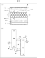
- FIG. 2 is a schematic cross-sectional view of the light-emitting device 41 according to the comparative example, and an energy diagram showing an example of Fermi level of each layer in the light-emitting element 42 of the light-emitting device 41, or an electron affinity and an ionization potential.
- the light emitting device 41 according to the comparative form is different from the light emitting device 1 according to this embodiment only in that the light emitting device 41 includes a light emitting element 42 including a hole transport layer 46 made of NiO.
- the light emitting device 41 also emits light according to the same principle as in the present embodiment.
- the hole transport barrier from the hole transport layer 46 to the quantum dot layer 8 is 0.5 to 1.5 eV.
- the light-emitting element 2 according to the present embodiment is made of an inorganic material, and includes a hole transport layer 6 having an ionization potential larger than 5.5 eV with respect to the vacuum level. For this reason, according to the light-emitting element 2 according to the present embodiment, as compared with the case where the hole-transporting layer 46 made of NiO is provided as in the light-emitting element 42 according to the comparative example, the quantum dots from the hole-transporting layer 6 The barrier for hole transport to the layer 8 can be reduced. Therefore, the light emitting device 1 according to the present embodiment can improve the light emission efficiency while ensuring the reliability.
- the hole transport layer 6 is made of LaNiO 3 as in the light emitting device 2 according to the present embodiment, CdSe / CdS, InP / ZnS, or ZnSe / ZnS is used as the quantum dot 16 of the quantum dot layer 8.
- the particle size of the quantum dots 16 is preferably 5 to 10 nm.
- the ionization potential of the hole transport layer 6 in this embodiment is preferably larger than the ionization potential of the quantum dot layer 8 or the difference from the ionization potential of the quantum dot layer 8 is 0.5 eV or less. If it is the said structure, the transport barrier from the hole transport layer 6 to the quantum dot layer 8 becomes smaller, and can transport a hole more efficiently from the hole transport layer 6 to the quantum dot layer 8.
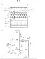
- FIG. 3A is a schematic cross-sectional view of the light emitting device 1 according to this embodiment.
- the light emitting device 1 according to this embodiment is configured only in that an electron blocking layer 18 is provided between the hole transport layer 6 and the quantum dot layer 8 as compared with the light emitting device 1 according to the previous embodiment. Is different.
- the electron blocking layer 18 is a layer having a function of inhibiting leakage of electrons from the quantum dot layer 8 to the hole transport layer 6 side.
- the electron blocking layer 18 may include an inorganic material such as Cu2O, LiNbO3, LiCoO2, Al2O3, SiO2, or SiN, and may include an organic material such as PVK, TFB, or poly-TPD.
- FIG. 3B is an energy diagram showing an example of Fermi levels or electron affinity and ionization potential in each layer of the light emitting device 2 according to this embodiment.
- an electron blocking layer 18 is shown between the hole transport layer 6 and the quantum dot layer 8 as compared with FIG.
- FIG. 3B shows an example in which the electronic block layer 18 is made of PVK.
- the electron block layer 18 in this embodiment has an ionization potential of 5.8 eV and an electron affinity of 2.2 eV.
- the electron block layer 18 has an electron affinity smaller than the electron affinity of the hole transport layer 6 and the quantum dot layer 8.
- the electron blocking layer 18 preferably has an ionization potential smaller than the ionization potential of at least one of the hole transport layer 6 and the quantum dot layer 8.
- the light emitting device 1 when a potential difference is generated between the first electrode 4 and the second electrode 12, holes and electrons are injected as in the previous embodiment.
- the holes transported from the first electrode 4 to the hole transport layer 6 are transported to the quantum dot layer 8 as indicated by an arrow H3.
- the ionization potential of the electron blocking layer 18 is smaller than the ionization potential of the hole transport layer 6 and the quantum dot layer 8, so that the hole transport layer 6 to the quantum dot layer This is because the barrier to hole transport to 8 does not increase.
- the electrons transported from the second electrode 12 to the quantum dot layer 8 via the electron transport layer 10 further move toward the electron block layer 18 as indicated by an arrow E3.
- the electron block layer 18 has an electron affinity smaller than the electron affinity of the quantum dot layer 8
- the barrier for electron injection from the quantum dot layer 8 to the electron block layer 18 is increased. For this reason, injection of electrons transported to the quantum dot layer 8 into the electron block layer 18 is inhibited, and leakage of electrons to the hole transport layer 6 and the first electrode 4 is reduced.
- the light-emitting element 2 in the present embodiment includes an electron block layer 18 that inhibits injection of electrons from the quantum dot layer 8 to the hole transport layer 6. For this reason, in the light emitting device 1 according to this embodiment, it is possible to reduce leakage of electrons transported to the quantum dot layer 8 to the hole transport layer 6 as compared with the light emitting device 1 in the previous embodiment. Therefore, the efficiency of recombination of holes and electrons in the quantum dot layer 8 can be improved, and the light emission efficiency of the light emitting device 1 can be improved.
- the electron affinity of the electron blocking layer 18 is smaller than 3.5 eV, more preferably smaller than 3.0 eV.
- the electron affinity of the electron block layer 18 is 0.5 eV or less smaller than the electron affinity of the quantum dot layer 8. If it is the said structure, the electronic block layer 18 can inhibit the electron leakage mentioned above efficiently.
- the film thickness of the electron block layer 18 is preferably 2 to 40 nm. Furthermore, the electron block layer 18 may be formed of NiO. In this case, the thickness of the electron blocking layer 18 is preferably 2 to 20 nm so that holes transported from the hole transporting layer 6 to the electron blocking layer 18 do not remain in the electron blocking layer 18.
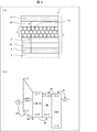
- FIG. 4A is a schematic cross-sectional view of the light emitting device 1 according to this embodiment.
- the light emitting device 1 according to the present embodiment is only in that a hole injection layer 20 is provided between the first electrode 4 and the hole transport layer 6 as compared with the light emitting device 1 according to the first embodiment.
- the configuration is different.
- the hole injection layer 20 is a layer having a function of injecting holes from the first electrode 4 and injecting holes into the hole transport layer 6.
- the hole injection layer 20 may include, for example, NiO, LiNbO 3 , LiCoO 3 , or Cu 2 O.
- FIG. 4B is an energy diagram showing an example of Fermi levels or electron affinity and ionization potential in each layer of the light emitting device 2 according to this embodiment.
- a hole injection layer 20 is shown between the first electrode 4 and the hole transport layer 6 as compared with FIG.
- FIG. 4B shows an example in which the hole injection layer 20 is made of NiO.
- the hole injection layer 20 in this embodiment has an ionization potential of 5.5 eV and an electron affinity of 2.0 eV.
- the hole injection layer 20 has an ionization potential between the Fermi level of the first electrode 4 and the ionization potential of the hole transport layer 6.
- the film thickness of the hole injection layer 20 is preferably 5 to 40 nm.
- the light emitting device 1 when a potential difference is generated between the first electrode 4 and the second electrode 12, holes are injected from the first electrode 4 into the hole injection layer 20 as indicated by an arrow H ⁇ b> 4.
- the barrier for hole injection from the first electrode 4 to the hole injection layer 20 is 0.9 eV.
- the holes injected into the hole injection layer 20 are injected from the hole injection layer 20 into the hole transport layer 6 as indicated by an arrow H5.
- the barrier for hole injection from the hole injection layer 20 to the hole transport layer 6 is 0.5 eV. Subsequent hole transport and electrons may be transported as in the first embodiment.
- holes are transported from the first electrode 4 to the hole transport layer 6 through the hole injection layer 20.
- the hole injection from the first electrode 4 is higher than the hole injection barrier from the first electrode 4 to the hole transport layer 6.
- the barrier for hole injection into the layer 20 or the hole injection from the hole injection layer 20 to the hole transport layer 6 is small. Therefore, holes can be efficiently transported from the first electrode 4 to the hole transport layer 6.
- holes can be more efficiently injected into the quantum dot layer 8 than the light emitting device 1 in the previous embodiment, and the light emission efficiency of the light emitting device 1 can be improved. Can be improved.
- FIG. 5 is a schematic cross-sectional view of a light-emitting device 1 according to a modification of the present embodiment, and an energy diagram showing an example of Fermi levels of each layer or electron affinity and ionization potential in the light-emitting element 2 of the light-emitting device 1. .
- the light emitting device 1 according to this modification is configured only in that an electron blocking layer 18 is provided between the hole transport layer 6 and the quantum dot layer 8 as compared with the light emitting device 1 according to this embodiment. Is different.
- the hole transport layer 6 is transferred from the first electrode 4 through the hole injection layer 20. Holes are injected. Next, holes are transported from the hole transport layer 6 to the quantum dot layer 8 in the same manner as the light emitting device 2 according to the second embodiment. In the transport of electrons in the light emitting device 2 according to this modification, electrons are transported from the second electrode 12 to the quantum dot layer 8 through the electron transport layer 10 as in the light emitting device 2 according to the second embodiment. The electrons transported to the quantum dot layer 8 are inhibited from being injected into the hole transport layer 6 by the electron block layer 18.
- the light emitting device 1 according to the present modification like the light emitting device 1 according to the present embodiment, maintains the efficiency of transporting holes to the quantum dot layer 8 while maintaining the efficiency from the quantum dot layer 8 to the hole transport layer 6. Blocks electron injection. Therefore, the efficiency of recombination of holes and electrons in the quantum dot layer 8 is further improved, and the light emission efficiency of the light emitting device 1 can be further improved.
- FIG. 6A is a schematic cross-sectional view of the light emitting device 1 according to this embodiment.
- the light emitting device 1 according to the present embodiment is different from the light emitting device 1 according to the third embodiment only in that a hole injection layer 22 is provided instead of the hole injection layer 20.
- the hole injection layer 22 is made of NiO and LaNiO 3 .
- the NiO density gradually decreases and the LaNiO 3 density gradually increases from the end face on the first electrode 4 side to the end face on the hole transport layer 6 side. That is, the hole injection layer 22 is made of NiO at the end face in contact with the first electrode 4, and NiO is gradually replaced with LaNiO 3 toward the hole transport layer 6, and the end face in contact with the hole transport layer 6 is made of LaNiO 3.
- the thickness of the hole injection layer 22 is preferably 5 to 40 nm.
- the hole injection layer 22 can be manufactured by simultaneously sputtering NiO and LaO.
- NiO and LaO may be sputtered simultaneously by keeping the power of the sputtering apparatus for depositing NiO constant and gradually increasing the power of the sputtering apparatus for depositing LaO.
- FIG. 6B is an energy diagram showing an example of Fermi levels or electron affinity and ionization potential in each layer of the light emitting device 2 according to this embodiment.
- a hole injection layer 22 is shown instead of the hole injection layer 20, as compared with FIG.
- the composition of the hole injection layer 22 in this embodiment is changed from NiO to LaNiO 3 from the end face on the first electrode 4 side to the end face on the hole transport layer 6 side. Reflecting this, as shown in FIG. 6B, the apparent ionization potential of the hole injection layer 22 is 5.5 eV to 6.0 eV from the first electrode 4 to the hole transport layer 6. Has increased. Also, as shown in FIG. 6B, the apparent electron affinity of the hole injection layer 22 also increases from 2.0 eV to 3.7 eV from the first electrode 4 to the hole transport layer 6. Yes.
- the light emitting device 1 when a potential difference is generated between the first electrode 4 and the second electrode 12, holes are injected from the first electrode 4 into the hole injection layer 22 as indicated by an arrow H4. Next, the holes injected into the hole injection layer 22 are transported through the hole injection layer 22 from the first electrode 4 toward the hole transport layer 6 as indicated by an arrow H6.
- the hole transport barrier in the hole injection layer 22 is small. Further, since the ionization potential between the end surface of the hole injection layer 22 on the hole transport layer 6 side and the hole transport layer 6 does not substantially change, a barrier for hole injection from the hole injection layer 22 to the hole transport layer 6 is achieved. Is very small.
- holes are injected from the first electrode 4 into the hole transport layer 6 through the hole injection layer 22. Subsequent hole transport and electrons may be transported as in the first embodiment.
- holes are transported from the first electrode 4 to the hole transport layer 6 through the hole injection layer 22. For this reason, the injection of holes from the hole injection layer 22 to the hole transport layer 6 is performed more efficiently. Therefore, in the light emitting device 1 according to the present embodiment, holes can be more efficiently transported to the quantum dot layer 8 than the light emitting device 1 in the previous embodiment, and the light emission efficiency of the light emitting device 1 can be improved. Can be improved.
- FIG. 7 is a schematic cross-sectional view of a light-emitting device 1 according to a modification of the present embodiment, and an energy diagram showing an example of Fermi levels of each layer or electron affinity and ionization potential in the light-emitting element 2 of the light-emitting device 1. .
- the light emitting device 1 according to this modification is configured only in that an electron blocking layer 18 is provided between the hole transport layer 6 and the quantum dot layer 8 as compared with the light emitting device 1 according to this embodiment. Is different.
- the hole transport layer 6 is transferred from the first electrode 4 through the hole injection layer 22. Holes are injected. Next, holes are transported from the hole transport layer 6 to the quantum dot layer 8 in the same manner as the light emitting device 2 according to the second embodiment. In the transport of electrons in the light emitting device 2 according to this modification, electrons are injected from the second electrode 12 into the quantum dot layer 8 through the electron transport layer 10 as in the light emitting device 2 according to the second embodiment. The electrons injected into the quantum dot layer 8 are inhibited from being injected into the hole transport layer 6 by the electron block layer 18.
- the light emitting device 1 according to the present modification like the light emitting device 1 according to the present embodiment, maintains the efficiency of transporting holes to the quantum dot layer 8 while maintaining the efficiency from the quantum dot layer 8 to the hole transport layer 6. Blocks electron injection. Therefore, the efficiency of recombination of holes and electrons in the quantum dot layer 8 is further improved, and the light emission efficiency of the light emitting device 1 can be further improved.
- each of the above-described embodiments a structure including the light emitting element 2 including the first electrode, the hole transport layer, the quantum dot layer, the electron transport layer, and the second electrode in order from the lower layer on the array substrate 3.
- the light emitting device 1 having the above has been described as an example.
- each of the embodiments described above includes the second electrode, the electron transport layer, the quantum dot layer, the hole transport layer, and the first electrode on the array substrate 3 in the reverse order, that is, in order from the lower layer.
- the present invention can also be applied to a light emitting device 1 having a structure including the light emitting element 2.
- FIG. 8 is a block diagram showing the light emitting element manufacturing apparatus 30 according to each of the embodiments described above.
- the light emitting element manufacturing apparatus 30 may include a controller 32 and a film forming apparatus 34.
- the controller 32 may control the film forming apparatus 34.
- the film forming apparatus 34 may form each layer of the light emitting element 2.
- the light-emitting element according to aspect 1 includes a first electrode, a second electrode, a quantum dot layer between which the quantum dots are stacked, between the first electrode and the second electrode, and between the quantum dot layer and the first electrode. And a hole transport layer made of LaNiO 3 .
- the light-emitting element according to aspect 2 includes a first electrode, a second electrode, a quantum dot layer in which quantum dots are stacked between the first electrode and the second electrode, and between the quantum dot layer and the first electrode. And a hole transport layer having an ionization potential larger than 5.5 eV based on the vacuum level.
- the ionization potential of the hole transport layer is greater than the ionization potential of the quantum dot layer, or the difference in ionization potential between the quantum dot layer and the hole transport layer is 0.5 eV or less. is there.
- an electron block layer is provided between the quantum dot layer and the hole transport layer, and the electron affinity of the electron block layer is smaller than the electron affinity of the hole transport layer.
- the electron affinity of the electron block layer is 0.5 eV or less smaller than the electron affinity of the quantum dot layer.
- the electron affinity of the electron block layer is smaller than 3.5 eV with respect to the vacuum level.
- a hole injection layer is provided between the first electrode and the hole transport layer, and the ionization potential of the hole injection layer is such that the Fermi level of the first electrode and the hole transport are Between the ionization potential of the layers.
- the hole injection layer is made of NiO and LaNiO 3, and in the hole injection layer, the density of NiO gradually decreases from the end surface on the first electrode side to the end surface on the hole transport layer side. However, the density of LaNiO 3 gradually increases.
- the light-emitting device includes the light-emitting element according to any of the above-described aspects.
- the light emitting element manufacturing apparatus includes a first electrode, a second electrode, a quantum dot layer in which quantum dots between the first electrode and the second electrode are stacked, the quantum dot layer, and the first electrode. And a hole transport layer made of LaNiO 3 .
- the light emitting device manufacturing apparatus includes a first electrode, a second electrode, a quantum dot layer in which quantum dots between the first electrode and the second electrode are stacked, the quantum dot layer, and the first electrode. And a hole transport layer which is made of an inorganic material and has an ionization potential larger than 5.5 eV with respect to the vacuum level.
Landscapes
- Physics & Mathematics (AREA)
- Optics & Photonics (AREA)
- Engineering & Computer Science (AREA)
- Manufacturing & Machinery (AREA)
- Chemical & Material Sciences (AREA)
- Crystallography & Structural Chemistry (AREA)
- Inorganic Chemistry (AREA)
- Nanotechnology (AREA)
- Electroluminescent Light Sources (AREA)
Abstract
For the purpose of improving the efficiency of hole injection from a hole transport layer to a quantum dot layer, provided is a light-emitting element (2) comprising: a first electrode (4); a second electrode (12); a quantum dot layer (8) which is disposed between the first electrode (4) and the second electrode (12), and in which quantum dots (16) are layered; and a hole transport layer (6) disposed between the quantum dot layer (8) and the first electrode (4), which is either a hole transport layer (6) that is formed from LaNiO3, or a hole transport layer (6) that is formed from an inorganic material and has an ionization potential greater than 5.5 eV with respect to vacuum level.
Description
本発明は、量子ドットを含む発光素子、当該発光素子を備えた発光デバイスおよび発光素子の製造装置に関する。
The present invention relates to a light emitting element including quantum dots, a light emitting device including the light emitting element, and a light emitting element manufacturing apparatus.
特許文献1は、半導体ナノクリスタルを含む発光デバイスを開示している。特許文献1の発光デバイスは、無機材料であるNiOからなる正孔輸送層を含む発光素子を備えている。無機材料からなる正孔輸送層を含む発光素子を備えた発光デバイスは、有機材料からなる正孔輸送層を含む発光素子を備えた発光デバイスと比較して、材料自体が酸素、水分、および紫外線等に対し安定であるため、発光デバイスの信頼性向上の面から好ましい。
Patent Document 1 discloses a light emitting device including a semiconductor nanocrystal. The light emitting device of Patent Document 1 includes a light emitting element including a hole transport layer made of NiO that is an inorganic material. A light emitting device including a light emitting element including a hole transport layer made of an inorganic material has oxygen, moisture, and ultraviolet light as compared with a light emitting device including a light emitting element including a hole transport layer made of an organic material. It is preferable from the viewpoint of improving the reliability of the light emitting device.
一般に、量子ドットのイオン化ポテンシャルは、真空準位を基準とすると、6~7eVである。また、無機材料であるNiOのイオン化ポテンシャルは、5.5eVである。このため、NiOと量子ドットとのイオン化ポテンシャルの差が0.5~1.5eVと大きい。
Generally, the ionization potential of quantum dots is 6 to 7 eV based on the vacuum level. The ionization potential of NiO, which is an inorganic material, is 5.5 eV. For this reason, the difference in ionization potential between NiO and quantum dots is as large as 0.5 to 1.5 eV.
このように、正孔輸送層に従来の無機材料を、量子ドット層に量子ドットを備えた発光素子においては、正孔輸送層から量子ドット層への正孔輸送の効率が悪い。したがって、正孔輸送層に従来の無機材料を採用した発光素子においては、正孔輸送層から量子ドット層への正孔の輸送効率と、電子輸送層から量子ドット層への電子の輸送効率とのバランスが悪くなり、発光素子の発光効率の低下に繋がる。
As described above, in a light emitting device having a conventional inorganic material for the hole transport layer and a quantum dot for the quantum dot layer, the efficiency of hole transport from the hole transport layer to the quantum dot layer is poor. Therefore, in a light emitting device employing a conventional inorganic material for the hole transport layer, the hole transport efficiency from the hole transport layer to the quantum dot layer and the electron transport efficiency from the electron transport layer to the quantum dot layer are This leads to a decrease in the light emission efficiency of the light emitting element.
上記課題を解決するために、本発明の発光素子は、第1電極と、第2電極と、第1電極と第2電極の間の、量子ドットが積層した量子ドット層と、前記量子ドット層と前記第1電極との間の、LaNiO3からなる正孔輸送層とを備える。
In order to solve the above problems, a light-emitting element of the present invention includes a first electrode, a second electrode, a quantum dot layer in which quantum dots are stacked between the first electrode and the second electrode, and the quantum dot layer. And a hole transport layer made of LaNiO 3 between the first electrode and the first electrode.
また、上記課題を解決するために、本発明の発光素子は、第1電極と、第2電極と、第1電極と第2電極の間の、量子ドットが積層した量子ドット層と、前記量子ドット層と前記第1電極との間の、無機材料からなり、真空準位を基準としたイオン化ポテンシャルが5.5eVよりも大きい正孔輸送層とを備える。
In order to solve the above problems, a light-emitting element of the present invention includes a first electrode, a second electrode, a quantum dot layer in which quantum dots are stacked between the first electrode and the second electrode, and the quantum A hole transport layer made of an inorganic material between the dot layer and the first electrode and having an ionization potential larger than 5.5 eV with respect to the vacuum level is provided.
また、上記課題を解決するために、本発明の発光素子の製造装置は、第1電極と、第2電極と、第1電極と第2電極の間の、量子ドットが積層した量子ドット層と、前記量子ドット層と前記第1電極との間の、LaNiO3からなる正孔輸送層とを形成する成膜装置を備える。
In order to solve the above problems, a light emitting device manufacturing apparatus according to the present invention includes a first electrode, a second electrode, a quantum dot layer in which quantum dots are stacked between the first electrode and the second electrode, and And a film forming apparatus for forming a hole transport layer made of LaNiO 3 between the quantum dot layer and the first electrode.
また、上記課題を解決するために、本発明の発光素子の製造装置は、第1電極と、第2電極と、第1電極と第2電極の間の、量子ドットが積層した量子ドット層と、前記量子ドット層と前記第1電極との間の、無機材料からなり、真空準位を基準としたイオン化ポテンシャルが5.5eVよりも大きい正孔輸送層とを形成する成膜装置を備える。
In order to solve the above problems, a light emitting device manufacturing apparatus according to the present invention includes a first electrode, a second electrode, a quantum dot layer in which quantum dots are stacked between the first electrode and the second electrode, and And a film forming apparatus for forming a hole transport layer made of an inorganic material and having an ionization potential larger than 5.5 eV based on a vacuum level, between the quantum dot layer and the first electrode.
上記構成により、無機材料を含む正孔輸送層を備えた発光素子において、正孔輸送層から量子ドット層への正孔の輸送効率が改善する。これにより、量子ドット層への正孔と電子との輸送効率のバランスが改善されるため、発光素子の信頼性を維持しつつ、発光素子の発光効率を向上させた発光デバイスを提供できる。
With the above configuration, in the light-emitting element including the hole transport layer containing an inorganic material, the hole transport efficiency from the hole transport layer to the quantum dot layer is improved. Thereby, since the balance of the transport efficiency of holes and electrons to the quantum dot layer is improved, it is possible to provide a light emitting device in which the light emission efficiency of the light emitting element is improved while maintaining the reliability of the light emitting element.
〔実施形態1〕
図1の(a)は、本実施形態に係る発光デバイス1の概略断面図である。Embodiment 1
FIG. 1A is a schematic cross-sectional view of alight emitting device 1 according to this embodiment.
図1の(a)は、本実施形態に係る発光デバイス1の概略断面図である。
FIG. 1A is a schematic cross-sectional view of a
図1の(a)に示すように、本実施形態に係る発光デバイス1は、発光素子2とアレイ基板3とを備える。発光デバイス1は、図示しないTFT(Thin Film Transistor)が形成されたアレイ基板3上に、発光素子2の各層が積層された構造を備える。なお、本明細書においては、発光デバイス1の発光素子2からアレイ基板3への方向を「下方向」、発光素子2のアレイ基板3から発光素子2への方向を「上方向」として記載する。
As shown in FIG. 1A, a light emitting device 1 according to this embodiment includes a light emitting element 2 and an array substrate 3. The light emitting device 1 has a structure in which each layer of the light emitting element 2 is laminated on an array substrate 3 on which TFTs (Thin Film Transistors) (not shown) are formed. In this specification, the direction from the light emitting element 2 of the light emitting device 1 to the array substrate 3 is described as “downward”, and the direction of the light emitting element 2 from the array substrate 3 to the light emitting element 2 is described as “upward”. .
発光素子2は、第1電極4上に、正孔輸送層6と、量子ドット層8と、電子輸送層10と、第2電極12とを、下層からこの順に備える。アレイ基板3の上層に形成された発光素子2の第1電極4は、アレイ基板3のTFTと電気的に接続されている。
The light-emitting element 2 includes a hole transport layer 6, a quantum dot layer 8, an electron transport layer 10, and a second electrode 12 in this order from the lower layer on the first electrode 4. The first electrode 4 of the light emitting element 2 formed on the upper layer of the array substrate 3 is electrically connected to the TFT of the array substrate 3.
第1電極4および第2電極12は導電性材料を含み、それぞれ、正孔輸送層6および電子輸送層10と電気的に接続されている。本実施形態においては、第1電極4はアノードであり、第2電極12はカソードである。
The first electrode 4 and the second electrode 12 include a conductive material, and are electrically connected to the hole transport layer 6 and the electron transport layer 10, respectively. In the present embodiment, the first electrode 4 is an anode and the second electrode 12 is a cathode.
第1電極4と第2電極12との何れか一方は、透明電極である。透明電極としては、例えば、ITO、IZO、ZnO、AZO、またはBZO等が用いられ、スパッタ法等によって成膜されてもよい。また、第1電極4または第2電極12のいずれか一方は金属材料を含んでいてもよく、金属材料としては、可視光の反射率の高いAl、Cu、Au、またはAg等が好ましい。
One of the first electrode 4 and the second electrode 12 is a transparent electrode. As the transparent electrode, for example, ITO, IZO, ZnO, AZO, or BZO is used, and the film may be formed by a sputtering method or the like. Moreover, either the 1st electrode 4 or the 2nd electrode 12 may contain the metal material, and as a metal material, Al, Cu, Au, Ag, etc. with a high visible light reflectance are preferable.
量子ドット層8は、量子ドット(半導体ナノ粒子)16が1から数層積層したものである。量子ドット層8は、ヘキサンまたはトルエン等の溶媒に量子ドット16を分散させた分散液から、スピンコート法、またはインクジェット法等によって製膜することができる。分散液にはチオール、アミン等分散材料を混合してもよい。量子ドット層8の膜厚は、5~50nmが好ましい。
The quantum dot layer 8 is formed by laminating one to several layers of quantum dots (semiconductor nanoparticles) 16. The quantum dot layer 8 can be formed from a dispersion liquid in which the quantum dots 16 are dispersed in a solvent such as hexane or toluene by a spin coating method, an inkjet method, or the like. A dispersion material such as thiol or amine may be mixed in the dispersion. The film thickness of the quantum dot layer 8 is preferably 5 to 50 nm.
量子ドット16は、価電子帯準位と伝導帯準位とを有し、価電子帯準位の正孔と伝導帯準位の電子との再結合によって発光する発光材料である。量子ドット16からの発光は、量子閉じ込め効果により狭いスペクトルを有するため、比較的深い色度の発光を得ることが可能である。
The quantum dot 16 is a light emitting material that has a valence band level and a conduction band level and emits light by recombination of holes in the valence band level and electrons in the conduction band level. The light emitted from the quantum dot 16 has a narrow spectrum due to the quantum confinement effect, and therefore, light having a relatively deep chromaticity can be obtained.
量子ドット16としては、例えば、コアにCdSe、シェルにZnSを備えた、コア/シェル構造を有する半導体ナノ粒子であってもよい。この他、量子ドット16は、CdSe/CdS、InP/ZnS、ZnSe/ZnSまたはCIGS/ZnS等をコア/シェル構造として有していてもよい。
The quantum dots 16 may be, for example, semiconductor nanoparticles having a core / shell structure with CdSe in the core and ZnS in the shell. In addition, the quantum dots 16 may have CdSe / CdS, InP / ZnS, ZnSe / ZnS, CIGS / ZnS, or the like as a core / shell structure.
量子ドット16の粒径は3~15nm程度である。量子ドット16からの発光の波長は、量子ドット16の粒径によって制御することができる。このため、量子ドット16の粒径を制御することにより、発光デバイス1が発する光の波長を制御できる。
The particle size of the quantum dots 16 is about 3 to 15 nm. The wavelength of light emitted from the quantum dot 16 can be controlled by the particle size of the quantum dot 16. For this reason, the wavelength of the light emitted from the light emitting device 1 can be controlled by controlling the particle size of the quantum dots 16.
正孔輸送層6は、第1電極4からの正孔を量子ドット層8へと輸送する層である。正孔輸送層は、無機材料からなり、真空準位を基準としたイオン化ポテンシャルが5.5eVよりも大きい。本実施形態において、正孔輸送層6はLaNiO3からなる。正孔輸送層6は、スパッタ法によって製膜されてもよい。正孔輸送層6の膜厚は、5~40nmが好ましい。
The hole transport layer 6 is a layer that transports holes from the first electrode 4 to the quantum dot layer 8. The hole transport layer is made of an inorganic material, and has an ionization potential larger than 5.5 eV based on the vacuum level. In the present embodiment, the hole transport layer 6 is made of LaNiO 3 . The hole transport layer 6 may be formed by sputtering. The thickness of the hole transport layer 6 is preferably 5 to 40 nm.
電子輸送層10は、第2電極12からの電子を量子ドット層8へと輸送する層である。電子輸送層10は、正孔の輸送を阻害する機能を有していてもよい。電子輸送層10は、例えば、ZnO、TiO2、Ta2O3、またはSrTiO3等を含んでいてもよく、スパッタ法によって製膜されてもよい。電子輸送層10の膜厚は、従来公知の膜厚を採用でき、10~100nmが好ましい。
The electron transport layer 10 is a layer that transports electrons from the second electrode 12 to the quantum dot layer 8. The electron transport layer 10 may have a function of inhibiting hole transport. The electron transport layer 10 may contain, for example, ZnO, TiO 2 , Ta 2 O 3 , SrTiO 3 or the like, and may be formed by sputtering. The film thickness of the electron transport layer 10 can employ a conventionally known film thickness, and is preferably 10 to 100 nm.
正孔輸送層および電子輸送層は、それぞれ、ナノ粒子、結晶、多結晶、またはアモルファスであってもよい。
The hole transport layer and the electron transport layer may be nanoparticles, crystals, polycrystals, or amorphous, respectively.
図1の(b)は、本実施形態に係る発光素子2の各層におけるフェルミ準位、または電子親和力とイオン化ポテンシャルとの例を示すエネルギー図である。図1の(b)においては、左から右に向かって、第1電極4、正孔輸送層6、量子ドット層8、電子輸送層10、および第2電極12を表している。
FIG. 1B is an energy diagram showing an example of Fermi levels or electron affinity and ionization potential in each layer of the light emitting device 2 according to this embodiment. In FIG. 1B, the first electrode 4, the hole transport layer 6, the quantum dot layer 8, the electron transport layer 10, and the second electrode 12 are shown from left to right.
第1電極4および第2電極12においては、それぞれの電極のフェルミ準位を、eVを単位に示す。正孔輸送層6、量子ドット層8、および電子輸送層10の下方においては、真空準位を基準とした、それぞれの層のイオン化ポテンシャルを、eVを単位に示す。正孔輸送層6、量子ドット層8、および電子輸送層10の上方においては、真空準位を基準とした、それぞれの層の電子親和力を、eVを単位に示す。
In the first electrode 4 and the second electrode 12, the Fermi level of each electrode is shown in eV. Below the hole transport layer 6, the quantum dot layer 8, and the electron transport layer 10, the ionization potential of each layer based on the vacuum level is shown in units of eV. Above the hole transport layer 6, the quantum dot layer 8, and the electron transport layer 10, the electron affinity of each layer based on the vacuum level is expressed in units of eV.
以下、本明細書において、単にイオン化ポテンシャルまたは電子親和力を説明する場合、何れも、真空準位を基準としたものとして説明を行う。
Hereinafter, in the present specification, when only the ionization potential or the electron affinity is described, the description will be made assuming that the vacuum level is the reference.
本実施形態においては、例として、第1電極4がITOから、第2電極12がAlからなる場合を図1の(b)に示す。この場合、第1電極4のフェルミ準位は4.6eVであり、第2電極12のフェルミ準位は4.3eVである。
In the present embodiment, as an example, a case where the first electrode 4 is made of ITO and the second electrode 12 is made of Al is shown in FIG. In this case, the Fermi level of the first electrode 4 is 4.6 eV, and the Fermi level of the second electrode 12 is 4.3 eV.
本実施形態においては、正孔輸送層6はLaNiO3からなる。このため、正孔輸送層6のイオン化ポテンシャルは6.0eVであり、正孔輸送層6の電子親和力は3.7eVである。また、本実施形態においては、例として、電子輸送層10がZnOからなる場合を図1の(b)に示す。この場合、電子輸送層10のイオン化ポテンシャルは7.4eVであり、電子輸送層10の電子親和力は4.0eVである。また、本実施形態においては、量子ドット16の材料および粒径によって変化するものの、量子ドット層8におけるイオン化ポテンシャルは、6~7eVであり、電子親和力は3.5~4.0eVである。
In the present embodiment, the hole transport layer 6 is made of LaNiO 3 . For this reason, the ionization potential of the hole transport layer 6 is 6.0 eV, and the electron affinity of the hole transport layer 6 is 3.7 eV. Moreover, in this embodiment, the case where the electron carrying layer 10 consists of ZnO is shown as an example in FIG.1 (b). In this case, the ionization potential of the electron transport layer 10 is 7.4 eV, and the electron affinity of the electron transport layer 10 is 4.0 eV. In this embodiment, the ionization potential in the quantum dot layer 8 is 6 to 7 eV and the electron affinity is 3.5 to 4.0 eV, although it varies depending on the material and particle size of the quantum dots 16.
本実施形態に係る発光デバイス1の発光機構について、図1を参照して説明する。
The light emission mechanism of the light emitting device 1 according to the present embodiment will be described with reference to FIG.
発光デバイス1において、第1電極4と第2電極12との間に電位差をかけることにより、第1電極4からは正孔が、第2電極12からは電子が、量子ドット層8に向かって注入される。図1の(a)の矢印h+に示すように、第1電極4からの正孔は、正孔輸送層6を介して、量子ドット層8に到達する。図1の(a)の矢印e-に示すように、第2電極12からの電子は、電子輸送層10を介して、量子ドット層8に到達する。
In the light emitting device 1, by applying a potential difference between the first electrode 4 and the second electrode 12, holes from the first electrode 4 and electrons from the second electrode 12 are directed toward the quantum dot layer 8. Injected. As indicated by an arrow h + in FIG. 1A, holes from the first electrode 4 reach the quantum dot layer 8 through the hole transport layer 6. As indicated by an arrow e− in FIG. 1A, electrons from the second electrode 12 reach the quantum dot layer 8 via the electron transport layer 10.
量子ドット層8に到達した正孔と電子とは、量子ドット16において再結合し、発光する。量子ドット16からの発光は、例えば、金属電極である第2電極によって反射され、透明電極である第1電極4、およびアレイ基板3を透過して、発光デバイス1の外部に放射されてもよい。
The holes and electrons that have reached the quantum dot layer 8 recombine at the quantum dots 16 and emit light. The light emitted from the quantum dots 16 may be reflected by the second electrode that is a metal electrode, transmitted through the first electrode 4 that is a transparent electrode, and the array substrate 3, and emitted to the outside of the light emitting device 1, for example. .
発光素子2の各層において、正孔および電子が輸送される様子を、図1の(b)を参照して説明する。
A state where holes and electrons are transported in each layer of the light emitting element 2 will be described with reference to FIG.
発光デバイス1において、第1電極4と第2電極12との間に電位差が発生すると、図1の(b)の矢印H1に示すように、第1電極4から正孔輸送層6へと正孔が注入される。同様に、図1の(b)の矢印E1に示すように、第2電極12から電子輸送層10へと電子が注入される。
In the light emitting device 1, when a potential difference is generated between the first electrode 4 and the second electrode 12, the positive electrode 4 is positively transferred from the first electrode 4 to the hole transport layer 6 as indicated by an arrow H <b> 1 in FIG. Holes are injected. Similarly, electrons are injected from the second electrode 12 into the electron transport layer 10 as indicated by an arrow E1 in FIG.
次いで、図1の(b)の矢印H2に示すように、正孔輸送層6から量子ドット層8へと正孔が輸送される。ここで、正孔輸送層6から量子ドット層8への正孔輸送の障壁は、量子ドット層8のイオン化ポテンシャルから正孔輸送層6のイオン化ポテンシャルを差し引いたエネルギーによって示される。したがって、本実施形態における正孔輸送層6から量子ドット層8への正孔輸送の障壁は、0~1.0eVである。
Next, holes are transported from the hole transport layer 6 to the quantum dot layer 8 as indicated by an arrow H2 in FIG. Here, the barrier for hole transport from the hole transport layer 6 to the quantum dot layer 8 is indicated by the energy obtained by subtracting the ionization potential of the hole transport layer 6 from the ionization potential of the quantum dot layer 8. Therefore, the hole transport barrier from the hole transport layer 6 to the quantum dot layer 8 in this embodiment is 0 to 1.0 eV.
同様に、図1の(b)の矢印E2に示すように、電子輸送層10から量子ドット層8へと電子が輸送される。このようにして、量子ドット層8に輸送された正孔と電子とが、量子ドット16において再結合する。
Similarly, electrons are transported from the electron transport layer 10 to the quantum dot layer 8 as indicated by an arrow E2 in FIG. In this way, the holes and electrons transported to the quantum dot layer 8 are recombined in the quantum dots 16.
図2は、比較形態に係る発光デバイス41の概略断面図と、発光デバイス41の発光素子42における各層のフェルミ準位、または電子親和力とイオン化ポテンシャルとの例を示すエネルギー図である。比較形態に係る発光デバイス41は、本実施形態に係る発光デバイス1と比較して、NiOからなる正孔輸送層46を含む発光素子42を備える点においてのみ構成が異なる。
FIG. 2 is a schematic cross-sectional view of the light-emitting device 41 according to the comparative example, and an energy diagram showing an example of Fermi level of each layer in the light-emitting element 42 of the light-emitting device 41, or an electron affinity and an ionization potential. The light emitting device 41 according to the comparative form is different from the light emitting device 1 according to this embodiment only in that the light emitting device 41 includes a light emitting element 42 including a hole transport layer 46 made of NiO.
発光デバイス41においても、本実施形態と同様の原理によって発光する。この際、正孔輸送層46から量子ドット層8への正孔輸送の障壁は、0.5~1.5eVである。
The light emitting device 41 also emits light according to the same principle as in the present embodiment. At this time, the hole transport barrier from the hole transport layer 46 to the quantum dot layer 8 is 0.5 to 1.5 eV.
本実施形態に係る発光素子2は、無機材料からなり、真空準位を基準としたイオン化ポテンシャルが5.5eVよりも大きい正孔輸送層6を備える。このため、本実施形態に係る発光素子2によれば、比較形態に係る発光素子42のように、NiOからなる正孔輸送層46を備える場合と比較して、正孔輸送層6から量子ドット層8への正孔輸送の障壁を小さくできる。したがって、本実施形態に係る発光デバイス1は、信頼性を確保しつつ、発光効率を向上させることが可能である。
The light-emitting element 2 according to the present embodiment is made of an inorganic material, and includes a hole transport layer 6 having an ionization potential larger than 5.5 eV with respect to the vacuum level. For this reason, according to the light-emitting element 2 according to the present embodiment, as compared with the case where the hole-transporting layer 46 made of NiO is provided as in the light-emitting element 42 according to the comparative example, the quantum dots from the hole-transporting layer 6 The barrier for hole transport to the layer 8 can be reduced. Therefore, the light emitting device 1 according to the present embodiment can improve the light emission efficiency while ensuring the reliability.
本実施形態に係る発光素子2のように、正孔輸送層6がLaNiO3からなる場合、量子ドット層8の量子ドット16としては、CdSe/CdS、InP/ZnS、またはZnSe/ZnSを用いることが好ましい。また、量子ドット16の粒径は、5~10nmであることが好ましい。上記構成であれば、正孔輸送層6と量子ドット層8とのイオン化ポテンシャルの差をより小さくすることができるため、正孔を量子ドット層8に、より効率よく注入する発光素子2を実現できる。
When the hole transport layer 6 is made of LaNiO 3 as in the light emitting device 2 according to the present embodiment, CdSe / CdS, InP / ZnS, or ZnSe / ZnS is used as the quantum dot 16 of the quantum dot layer 8. Is preferred. The particle size of the quantum dots 16 is preferably 5 to 10 nm. With the above configuration, since the difference in ionization potential between the hole transport layer 6 and the quantum dot layer 8 can be reduced, the light-emitting element 2 that injects holes into the quantum dot layer 8 more efficiently is realized. it can.
また、本実施形態における正孔輸送層6のイオン化ポテンシャルは、量子ドット層8のイオン化ポテンシャルよりも大きい、または量子ドット層8のイオン化ポテンシャルとの差が0.5eV以下であることが好ましい。上記構成であれば、正孔輸送層6から量子ドット層8への輸送障壁はより小さくなり、正孔輸送層6から量子ドット層8へより効率よく正孔を輸送できる。
Further, the ionization potential of the hole transport layer 6 in this embodiment is preferably larger than the ionization potential of the quantum dot layer 8 or the difference from the ionization potential of the quantum dot layer 8 is 0.5 eV or less. If it is the said structure, the transport barrier from the hole transport layer 6 to the quantum dot layer 8 becomes smaller, and can transport a hole more efficiently from the hole transport layer 6 to the quantum dot layer 8.
〔実施形態2〕
図3の(a)は、本実施形態に係る発光デバイス1の概略断面図である。本実施形態に係る発光デバイス1は、前実施形態に係る発光デバイス1と比較して、正孔輸送層6と量子ドット層8との間に、電子ブロック層18を備えている点においてのみ構成が異なる。 [Embodiment 2]
FIG. 3A is a schematic cross-sectional view of thelight emitting device 1 according to this embodiment. The light emitting device 1 according to this embodiment is configured only in that an electron blocking layer 18 is provided between the hole transport layer 6 and the quantum dot layer 8 as compared with the light emitting device 1 according to the previous embodiment. Is different.
図3の(a)は、本実施形態に係る発光デバイス1の概略断面図である。本実施形態に係る発光デバイス1は、前実施形態に係る発光デバイス1と比較して、正孔輸送層6と量子ドット層8との間に、電子ブロック層18を備えている点においてのみ構成が異なる。 [Embodiment 2]
FIG. 3A is a schematic cross-sectional view of the
電子ブロック層18は、量子ドット層8から正孔輸送層6側への電子のリークを阻害する機能を有する層である。電子ブロック層18は、Cu2O,LiNbO3、LiCoO2、Al2O3、SiO2、またはSiN等の無機材料を含んでいてもよく、PVK、TFB、またはpoly-TPD等の有機材料を含んでいてもよい。
The electron blocking layer 18 is a layer having a function of inhibiting leakage of electrons from the quantum dot layer 8 to the hole transport layer 6 side. The electron blocking layer 18 may include an inorganic material such as Cu2O, LiNbO3, LiCoO2, Al2O3, SiO2, or SiN, and may include an organic material such as PVK, TFB, or poly-TPD.
図3の(b)は、本実施形態に係る発光素子2の各層におけるフェルミ準位、または電子親和力とイオン化ポテンシャルとの例を示すエネルギー図である。図3の(b)においては、図1の(b)と比較して、正孔輸送層6と量子ドット層8との間に、電子ブロック層18が示されている。図3の(b)においては、電子ブロック層18がPVKからなる例を図示している。図3の(b)に示すように、本実施形態における電子ブロック層18は、イオン化ポテンシャルが5.8eVであり、電子親和力が2.2eVである。
FIG. 3B is an energy diagram showing an example of Fermi levels or electron affinity and ionization potential in each layer of the light emitting device 2 according to this embodiment. In FIG. 3B, an electron blocking layer 18 is shown between the hole transport layer 6 and the quantum dot layer 8 as compared with FIG. FIG. 3B shows an example in which the electronic block layer 18 is made of PVK. As shown in FIG. 3B, the electron block layer 18 in this embodiment has an ionization potential of 5.8 eV and an electron affinity of 2.2 eV.
このように、電子ブロック層18は、正孔輸送層6および量子ドット層8の電子親和力よりも小さい電子親和力を有する。また、電子ブロック層18は、正孔輸送層6および量子ドット層8の少なくとも一方のイオン化ポテンシャルより、小さいイオン化ポテンシャルを有することが好ましい。
Thus, the electron block layer 18 has an electron affinity smaller than the electron affinity of the hole transport layer 6 and the quantum dot layer 8. The electron blocking layer 18 preferably has an ionization potential smaller than the ionization potential of at least one of the hole transport layer 6 and the quantum dot layer 8.
発光素子2の各層において、正孔および電子が輸送される様子を、図3の(b)を参照して説明する。
A state where holes and electrons are transported in each layer of the light emitting element 2 will be described with reference to FIG.
発光デバイス1において、第1電極4と第2電極12との間に電位差が発生すると、前実施形態と同様に正孔および電子が注入される。ここで、本実施形態においては、第1電極4から正孔輸送層6へ輸送された正孔は、矢印H3に示すように、量子ドット層8へ輸送される。これは、図3の(b)に示すように、電子ブロック層18のイオン化ポテンシャルが、正孔輸送層6および量子ドット層8のイオン化ポテンシャルよりも小さいため、正孔輸送層6から量子ドット層8への正孔輸送の障壁が増加しないことによる。
In the light emitting device 1, when a potential difference is generated between the first electrode 4 and the second electrode 12, holes and electrons are injected as in the previous embodiment. Here, in the present embodiment, the holes transported from the first electrode 4 to the hole transport layer 6 are transported to the quantum dot layer 8 as indicated by an arrow H3. This is because, as shown in FIG. 3B, the ionization potential of the electron blocking layer 18 is smaller than the ionization potential of the hole transport layer 6 and the quantum dot layer 8, so that the hole transport layer 6 to the quantum dot layer This is because the barrier to hole transport to 8 does not increase.
また、本実施形態においては、第2電極12から電子輸送層10を経由して量子ドット層8に輸送された電子は、さらに、矢印E3に示すように、電子ブロック層18側に移動しようとする。しかしながら、電子ブロック層18は量子ドット層8の電子親和力よりも小さい電子親和力を有するため、量子ドット層8から電子ブロック層18への電子注入の障壁が大きくなる。このため、量子ドット層8に輸送された電子の、電子ブロック層18への注入が阻害され、正孔輸送層6および第1電極4への電子のリークが低減される。
In the present embodiment, the electrons transported from the second electrode 12 to the quantum dot layer 8 via the electron transport layer 10 further move toward the electron block layer 18 as indicated by an arrow E3. To do. However, since the electron block layer 18 has an electron affinity smaller than the electron affinity of the quantum dot layer 8, the barrier for electron injection from the quantum dot layer 8 to the electron block layer 18 is increased. For this reason, injection of electrons transported to the quantum dot layer 8 into the electron block layer 18 is inhibited, and leakage of electrons to the hole transport layer 6 and the first electrode 4 is reduced.
本実施形態における発光素子2は、量子ドット層8から正孔輸送層6への電子の注入を阻害する電子ブロック層18を備えている。このため、本実施形態に係る発光デバイス1においては、前実施形態における発光デバイス1と比較して、量子ドット層8へ輸送された電子が、正孔輸送層6へリークすることを低減できる。したがって、量子ドット層8における正孔と電子との再結合の効率を向上させ、発光デバイス1の発光効率を向上させることができる。
The light-emitting element 2 in the present embodiment includes an electron block layer 18 that inhibits injection of electrons from the quantum dot layer 8 to the hole transport layer 6. For this reason, in the light emitting device 1 according to this embodiment, it is possible to reduce leakage of electrons transported to the quantum dot layer 8 to the hole transport layer 6 as compared with the light emitting device 1 in the previous embodiment. Therefore, the efficiency of recombination of holes and electrons in the quantum dot layer 8 can be improved, and the light emission efficiency of the light emitting device 1 can be improved.
なお、電子ブロック層18の電子親和力は、3.5eVよりも小さく、より好ましくは、3.0eVよりも小さい。あるいは、電子ブロック層18の電子親和力は、量子ドット層8の電子親和力よりも0.5eV以上小さい。上記構成であれば、電子ブロック層18が効率よく上述した電子のリークを阻害できる。
Note that the electron affinity of the electron blocking layer 18 is smaller than 3.5 eV, more preferably smaller than 3.0 eV. Alternatively, the electron affinity of the electron block layer 18 is 0.5 eV or less smaller than the electron affinity of the quantum dot layer 8. If it is the said structure, the electronic block layer 18 can inhibit the electron leakage mentioned above efficiently.
また、電子ブロック層18の膜厚は、2~40nmが好ましい。さらに、電子ブロック層18はNiOから形成されていてもよい。この場合、正孔輸送層6から電子ブロック層18へ輸送された正孔が、電子ブロック層18に停留しないよう、電子ブロック層18の膜厚を2~20nmとすることが好ましい。
The film thickness of the electron block layer 18 is preferably 2 to 40 nm. Furthermore, the electron block layer 18 may be formed of NiO. In this case, the thickness of the electron blocking layer 18 is preferably 2 to 20 nm so that holes transported from the hole transporting layer 6 to the electron blocking layer 18 do not remain in the electron blocking layer 18.
〔実施形態3〕
図4の(a)は、本実施形態に係る発光デバイス1の概略断面図である。本実施形態に係る発光デバイス1は、実施形態1に係る発光デバイス1と比較して、第1電極4と正孔輸送層6との間に、正孔注入層20を備えている点においてのみ構成が異なる。 [Embodiment 3]
FIG. 4A is a schematic cross-sectional view of thelight emitting device 1 according to this embodiment. The light emitting device 1 according to the present embodiment is only in that a hole injection layer 20 is provided between the first electrode 4 and the hole transport layer 6 as compared with the light emitting device 1 according to the first embodiment. The configuration is different.
図4の(a)は、本実施形態に係る発光デバイス1の概略断面図である。本実施形態に係る発光デバイス1は、実施形態1に係る発光デバイス1と比較して、第1電極4と正孔輸送層6との間に、正孔注入層20を備えている点においてのみ構成が異なる。 [Embodiment 3]
FIG. 4A is a schematic cross-sectional view of the
正孔注入層20は、第1電極4から正孔が注入され、正孔輸送層6へ正孔を注入する機能を有する層である。正孔注入層20は、例えば、NiO、LiNbO3、LiCoO3、またはCu2Oを含んでいてもよい。
The hole injection layer 20 is a layer having a function of injecting holes from the first electrode 4 and injecting holes into the hole transport layer 6. The hole injection layer 20 may include, for example, NiO, LiNbO 3 , LiCoO 3 , or Cu 2 O.
図4の(b)は、本実施形態に係る発光素子2の各層におけるフェルミ準位、または電子親和力とイオン化ポテンシャルとの例を示すエネルギー図である。図4の(b)においては、図1の(b)と比較して、第1電極4と正孔輸送層6との間に、正孔注入層20が示されている。図4の(b)においては、正孔注入層20がNiOからなる例を図示している。図4の(b)に示すように、本実施形態における正孔注入層20は、イオン化ポテンシャルが5.5eVであり、電子親和力が2.0eVである。
FIG. 4B is an energy diagram showing an example of Fermi levels or electron affinity and ionization potential in each layer of the light emitting device 2 according to this embodiment. In FIG. 4B, a hole injection layer 20 is shown between the first electrode 4 and the hole transport layer 6 as compared with FIG. FIG. 4B shows an example in which the hole injection layer 20 is made of NiO. As shown in FIG. 4B, the hole injection layer 20 in this embodiment has an ionization potential of 5.5 eV and an electron affinity of 2.0 eV.
このように、正孔注入層20は、第1電極4のフェルミ準位と正孔輸送層6のイオン化ポテンシャルとの間のイオン化ポテンシャルを有する。正孔注入層20の膜厚は、5~40nmが好ましい。
Thus, the hole injection layer 20 has an ionization potential between the Fermi level of the first electrode 4 and the ionization potential of the hole transport layer 6. The film thickness of the hole injection layer 20 is preferably 5 to 40 nm.
発光素子2の各層において、正孔および電子が輸送される様子を、図4の(b)を参照して説明する。
A state in which holes and electrons are transported in each layer of the light emitting element 2 will be described with reference to FIG.
発光デバイス1において、第1電極4と第2電極12との間に電位差が発生すると、矢印H4に示すように、第1電極4から正孔注入層20へ正孔が注入される。第1電極4から正孔注入層20への正孔注入の障壁は、0.9eVである。次いで、正孔注入層20に注入された正孔は、矢印H5に示すように、正孔注入層20から正孔輸送層6へ注入される。正孔注入層20から正孔輸送層6への正孔注入の障壁は、0.5eVである。その後の正孔の輸送および電子は、実施形態1と同様に輸送されてもよい。
In the light emitting device 1, when a potential difference is generated between the first electrode 4 and the second electrode 12, holes are injected from the first electrode 4 into the hole injection layer 20 as indicated by an arrow H <b> 4. The barrier for hole injection from the first electrode 4 to the hole injection layer 20 is 0.9 eV. Next, the holes injected into the hole injection layer 20 are injected from the hole injection layer 20 into the hole transport layer 6 as indicated by an arrow H5. The barrier for hole injection from the hole injection layer 20 to the hole transport layer 6 is 0.5 eV. Subsequent hole transport and electrons may be transported as in the first embodiment.
本実施形態における発光素子2は、第1電極4から正孔輸送層6への正孔の輸送が、正孔注入層20を介して行われる。図1の(b)と、図4の(b)との比較からわかるように、第1電極4から正孔輸送層6への正孔注入の障壁よりも、第1電極4から正孔注入層20への正孔注入の障壁、または正孔注入層20から正孔輸送層6への正孔注入の障壁は小さい。ゆえに、効率的に第1電極4から正孔輸送層6への正孔の輸送を行うことができる。
In the light-emitting element 2 in the present embodiment, holes are transported from the first electrode 4 to the hole transport layer 6 through the hole injection layer 20. As can be seen from the comparison between FIG. 1B and FIG. 4B, the hole injection from the first electrode 4 is higher than the hole injection barrier from the first electrode 4 to the hole transport layer 6. The barrier for hole injection into the layer 20 or the hole injection from the hole injection layer 20 to the hole transport layer 6 is small. Therefore, holes can be efficiently transported from the first electrode 4 to the hole transport layer 6.
したがって、本実施形態に係る発光デバイス1においては、前実施形態における発光デバイス1と比較して、正孔をより効率的に量子ドット層8に注入することができ、発光デバイス1の発光効率を向上させることができる。
Therefore, in the light emitting device 1 according to the present embodiment, holes can be more efficiently injected into the quantum dot layer 8 than the light emitting device 1 in the previous embodiment, and the light emission efficiency of the light emitting device 1 can be improved. Can be improved.
図5は、本実施形態の変形例に係る発光デバイス1の概略断面図と、発光デバイス1の発光素子2における各層のフェルミ準位、または電子親和力とイオン化ポテンシャルとの例を示すエネルギー図である。本変形例に係る発光デバイス1は、本実施形態に係る発光デバイス1と比較して、正孔輸送層6と量子ドット層8との間に、電子ブロック層18を備えている点においてのみ構成が異なる。
FIG. 5 is a schematic cross-sectional view of a light-emitting device 1 according to a modification of the present embodiment, and an energy diagram showing an example of Fermi levels of each layer or electron affinity and ionization potential in the light-emitting element 2 of the light-emitting device 1. . The light emitting device 1 according to this modification is configured only in that an electron blocking layer 18 is provided between the hole transport layer 6 and the quantum dot layer 8 as compared with the light emitting device 1 according to this embodiment. Is different.
本変形例に係る発光素子2における正孔の輸送においては、始めに、本実施形態に係る発光素子2と同様に、第1電極4から正孔注入層20を介して正孔輸送層6に正孔が注入される。次いで、実施形態2に係る発光素子2と同様に、正孔輸送層6から量子ドット層8に正孔が輸送される。本変形例に係る発光素子2における電子の輸送においては、実施形態2に係る発光素子2と同様に、第2電極12から電子輸送層10を介して量子ドット層8に電子が輸送される。量子ドット層8に輸送された電子は、電子ブロック層18によって、正孔輸送層6への注入が阻害される。
In transporting holes in the light-emitting element 2 according to this modification, first, as in the light-emitting element 2 according to this embodiment, the hole transport layer 6 is transferred from the first electrode 4 through the hole injection layer 20. Holes are injected. Next, holes are transported from the hole transport layer 6 to the quantum dot layer 8 in the same manner as the light emitting device 2 according to the second embodiment. In the transport of electrons in the light emitting device 2 according to this modification, electrons are transported from the second electrode 12 to the quantum dot layer 8 through the electron transport layer 10 as in the light emitting device 2 according to the second embodiment. The electrons transported to the quantum dot layer 8 are inhibited from being injected into the hole transport layer 6 by the electron block layer 18.
本変形例に係る発光デバイス1は、本実施形態に係る発光デバイス1と同様に、量子ドット層8への正孔の輸送効率を維持しつつ、量子ドット層8から正孔輸送層6への電子の注入を阻害する。したがって、量子ドット層8における正孔と電子との再結合の効率がより改善し、発光デバイス1の発光効率をより向上させることができる。
The light emitting device 1 according to the present modification, like the light emitting device 1 according to the present embodiment, maintains the efficiency of transporting holes to the quantum dot layer 8 while maintaining the efficiency from the quantum dot layer 8 to the hole transport layer 6. Blocks electron injection. Therefore, the efficiency of recombination of holes and electrons in the quantum dot layer 8 is further improved, and the light emission efficiency of the light emitting device 1 can be further improved.
〔実施形態4〕
図6の(a)は、本実施形態に係る発光デバイス1の概略断面図である。本実施形態に係る発光デバイス1は、実施形態3に係る発光デバイス1と比較して、正孔注入層20の代わりに、正孔注入層22を備えている点においてのみ構成が異なる。 [Embodiment 4]
FIG. 6A is a schematic cross-sectional view of thelight emitting device 1 according to this embodiment. The light emitting device 1 according to the present embodiment is different from the light emitting device 1 according to the third embodiment only in that a hole injection layer 22 is provided instead of the hole injection layer 20.
図6の(a)は、本実施形態に係る発光デバイス1の概略断面図である。本実施形態に係る発光デバイス1は、実施形態3に係る発光デバイス1と比較して、正孔注入層20の代わりに、正孔注入層22を備えている点においてのみ構成が異なる。 [Embodiment 4]
FIG. 6A is a schematic cross-sectional view of the
正孔注入層22はNiOとLaNiO3とからなる。正孔注入層22においては、第1電極4側の端面から正孔輸送層6側の端面にかけて、次第にNiOの密度が低下し、次第にLaNiO3の密度が増大する。すなわち、正孔注入層22は、第1電極4と接する端面がNiOからなり、正孔輸送層6に向かって、次第にNiOがLaNiO3に置き換わり、正孔輸送層6と接する端面がLaNiO3からなる構造を備える。第1電極4から正孔輸送層6にかけて、次第に値が0から1に増加する変数Xを用いて上記を換言すれば、正孔注入層22は、LaXNiO2X+1と表される構造を備えていてもよい。本実施形態において、正孔輸送層6は、正孔注入層22と連続的に製膜されてもよい。正孔注入層22の膜厚は、5~40nmが好ましい。
The hole injection layer 22 is made of NiO and LaNiO 3 . In the hole injection layer 22, the NiO density gradually decreases and the LaNiO 3 density gradually increases from the end face on the first electrode 4 side to the end face on the hole transport layer 6 side. That is, the hole injection layer 22 is made of NiO at the end face in contact with the first electrode 4, and NiO is gradually replaced with LaNiO 3 toward the hole transport layer 6, and the end face in contact with the hole transport layer 6 is made of LaNiO 3. The structure which becomes. In other words, using the variable X whose value gradually increases from 0 to 1 from the first electrode 4 to the hole transport layer 6, the hole injection layer 22 has a structure represented as La X NiO 2X + 1. It may be. In the present embodiment, the hole transport layer 6 may be formed continuously with the hole injection layer 22. The thickness of the hole injection layer 22 is preferably 5 to 40 nm.
正孔注入層22は、NiOとLaOとを同時にスパッタすることにより製造することができる。たとえば、NiOを成膜するスパッタ装置のパワーを一定とし、LaOを成膜するスパッタ装置のパワーを徐々に増加させて、NiOとLaOとを同時にスパッタすればよい。
The hole injection layer 22 can be manufactured by simultaneously sputtering NiO and LaO. For example, NiO and LaO may be sputtered simultaneously by keeping the power of the sputtering apparatus for depositing NiO constant and gradually increasing the power of the sputtering apparatus for depositing LaO.
図6の(b)は、本実施形態に係る発光素子2の各層におけるフェルミ準位、または電子親和力とイオン化ポテンシャルとの例を示すエネルギー図である。図6の(b)においては、図4の(b)と比較して、正孔注入層20の代わりに正孔注入層22が示されている。
FIG. 6B is an energy diagram showing an example of Fermi levels or electron affinity and ionization potential in each layer of the light emitting device 2 according to this embodiment. In FIG. 6B, a hole injection layer 22 is shown instead of the hole injection layer 20, as compared with FIG.
本実施形態における正孔注入層22は、第1電極4側の端面から正孔輸送層6側の端面にかけて、NiOからLaNiO3に組成が置き換わる。このことを反映して、図6の(b)に示すように、正孔注入層22の見かけ上のイオン化ポテンシャルは、第1電極4から正孔輸送層6にかけて、5.5eVから6.0eVに増加している。また、図6の(b)に示すように、正孔注入層22の見かけ上の電子親和力においても、第1電極4から正孔輸送層6にかけて、2.0eVから3.7eVに増加している。
The composition of the hole injection layer 22 in this embodiment is changed from NiO to LaNiO 3 from the end face on the first electrode 4 side to the end face on the hole transport layer 6 side. Reflecting this, as shown in FIG. 6B, the apparent ionization potential of the hole injection layer 22 is 5.5 eV to 6.0 eV from the first electrode 4 to the hole transport layer 6. Has increased. Also, as shown in FIG. 6B, the apparent electron affinity of the hole injection layer 22 also increases from 2.0 eV to 3.7 eV from the first electrode 4 to the hole transport layer 6. Yes.
発光素子2の各層において、正孔および電子が輸送される様子を、図6の(b)を参照して説明する。
A state in which holes and electrons are transported in each layer of the light-emitting element 2 will be described with reference to FIG.
発光デバイス1において、第1電極4と第2電極12との間に電位差が発生すると、矢印H4に示すように、第1電極4から正孔注入層22へ正孔が注入される。次いで、正孔注入層22に注入された正孔は、矢印H6に示すように、第1電極4から正孔輸送層6に向かって正孔注入層22中を輸送される。
In the light emitting device 1, when a potential difference is generated between the first electrode 4 and the second electrode 12, holes are injected from the first electrode 4 into the hole injection layer 22 as indicated by an arrow H4. Next, the holes injected into the hole injection layer 22 are transported through the hole injection layer 22 from the first electrode 4 toward the hole transport layer 6 as indicated by an arrow H6.
正孔注入層22における見かけ上のイオン化ポテンシャルは、連続的に増加しているため、正孔注入層22中における正孔輸送の障壁は小さい。また、正孔注入層22の正孔輸送層6側の端面と正孔輸送層6とのイオン化ポテンシャルはほぼ変わらないため、正孔注入層22から正孔輸送層6への正孔注入の障壁は非常に小さい。
Since the apparent ionization potential in the hole injection layer 22 continuously increases, the hole transport barrier in the hole injection layer 22 is small. Further, since the ionization potential between the end surface of the hole injection layer 22 on the hole transport layer 6 side and the hole transport layer 6 does not substantially change, a barrier for hole injection from the hole injection layer 22 to the hole transport layer 6 is achieved. Is very small.
このため、第1電極4から正孔注入層22を介して正孔輸送層6へ正孔が注入される。その後の正孔の輸送および電子は、実施形態1と同様に輸送されてもよい。
Therefore, holes are injected from the first electrode 4 into the hole transport layer 6 through the hole injection layer 22. Subsequent hole transport and electrons may be transported as in the first embodiment.
本実施形態における発光素子2は、第1電極4から正孔輸送層6への正孔の輸送が、正孔注入層22を介して行われる。このため、正孔注入層22から正孔輸送層6への正孔の注入がより効率的に行われる。したがって、本実施形態に係る発光デバイス1においては、前実施形態における発光デバイス1と比較して、正孔をより効率的に量子ドット層8に輸送することができ、発光デバイス1の発光効率を向上させることができる。
In the light-emitting element 2 in the present embodiment, holes are transported from the first electrode 4 to the hole transport layer 6 through the hole injection layer 22. For this reason, the injection of holes from the hole injection layer 22 to the hole transport layer 6 is performed more efficiently. Therefore, in the light emitting device 1 according to the present embodiment, holes can be more efficiently transported to the quantum dot layer 8 than the light emitting device 1 in the previous embodiment, and the light emission efficiency of the light emitting device 1 can be improved. Can be improved.
図7は、本実施形態の変形例に係る発光デバイス1の概略断面図と、発光デバイス1の発光素子2における各層のフェルミ準位、または電子親和力とイオン化ポテンシャルとの例を示すエネルギー図である。本変形例に係る発光デバイス1は、本実施形態に係る発光デバイス1と比較して、正孔輸送層6と量子ドット層8との間に、電子ブロック層18を備えている点においてのみ構成が異なる。
FIG. 7 is a schematic cross-sectional view of a light-emitting device 1 according to a modification of the present embodiment, and an energy diagram showing an example of Fermi levels of each layer or electron affinity and ionization potential in the light-emitting element 2 of the light-emitting device 1. . The light emitting device 1 according to this modification is configured only in that an electron blocking layer 18 is provided between the hole transport layer 6 and the quantum dot layer 8 as compared with the light emitting device 1 according to this embodiment. Is different.
本変形例に係る発光素子2における正孔の輸送においては、始めに、本実施形態に係る発光素子2と同様に、第1電極4から正孔注入層22を介して正孔輸送層6に正孔が注入される。次いで、実施形態2に係る発光素子2と同様に、正孔輸送層6から量子ドット層8に正孔が輸送される。本変形例に係る発光素子2における電子の輸送においては、実施形態2に係る発光素子2と同様に、第2電極12から電子輸送層10を介して量子ドット層8に電子が注入される。量子ドット層8に注入された電子は、電子ブロック層18によって、正孔輸送層6への注入が阻害される。
In transporting holes in the light-emitting element 2 according to this modification, first, as in the light-emitting element 2 according to this embodiment, the hole transport layer 6 is transferred from the first electrode 4 through the hole injection layer 22. Holes are injected. Next, holes are transported from the hole transport layer 6 to the quantum dot layer 8 in the same manner as the light emitting device 2 according to the second embodiment. In the transport of electrons in the light emitting device 2 according to this modification, electrons are injected from the second electrode 12 into the quantum dot layer 8 through the electron transport layer 10 as in the light emitting device 2 according to the second embodiment. The electrons injected into the quantum dot layer 8 are inhibited from being injected into the hole transport layer 6 by the electron block layer 18.
本変形例に係る発光デバイス1は、本実施形態に係る発光デバイス1と同様に、量子ドット層8への正孔の輸送効率を維持しつつ、量子ドット層8から正孔輸送層6への電子の注入を阻害する。したがって、量子ドット層8における正孔と電子との再結合の効率がより改善し、発光デバイス1の発光効率をより向上させることができる。
The light emitting device 1 according to the present modification, like the light emitting device 1 according to the present embodiment, maintains the efficiency of transporting holes to the quantum dot layer 8 while maintaining the efficiency from the quantum dot layer 8 to the hole transport layer 6. Blocks electron injection. Therefore, the efficiency of recombination of holes and electrons in the quantum dot layer 8 is further improved, and the light emission efficiency of the light emitting device 1 can be further improved.
上述の各実施形態においては、アレイ基板3上に、下層から順に、第1電極、正孔輸送層、量子ドット層、電子輸送層、および第2電極を備えた発光素子2を備えた構造を有する発光デバイス1を例に挙げて説明した。しかしながら、上述の各実施形態は、アレイ基板3上に、各層を逆順に、すなわち、下層から順に、第2電極、電子輸送層、量子ドット層、正孔輸送層、および第1電極を備えた発光素子2を備えた構造を有する発光デバイス1においても適用できる。
In each of the above-described embodiments, a structure including the light emitting element 2 including the first electrode, the hole transport layer, the quantum dot layer, the electron transport layer, and the second electrode in order from the lower layer on the array substrate 3. The light emitting device 1 having the above has been described as an example. However, each of the embodiments described above includes the second electrode, the electron transport layer, the quantum dot layer, the hole transport layer, and the first electrode on the array substrate 3 in the reverse order, that is, in order from the lower layer. The present invention can also be applied to a light emitting device 1 having a structure including the light emitting element 2.
図8は、上述の各実施形態に係る発光素子の製造装置30を示すブロック図である。発光素子の製造装置30は、コントローラ32と、成膜装置34とを備えていてもよい。コントローラ32は、成膜装置34を制御してもよい。成膜装置34は、発光素子2の各層を成膜してもよい。
FIG. 8 is a block diagram showing the light emitting element manufacturing apparatus 30 according to each of the embodiments described above. The light emitting element manufacturing apparatus 30 may include a controller 32 and a film forming apparatus 34. The controller 32 may control the film forming apparatus 34. The film forming apparatus 34 may form each layer of the light emitting element 2.
〔まとめ〕
様態1の発光素子は、第1電極と、第2電極と、第1電極と第2電極の間の、量子ドットが積層した量子ドット層と、前記量子ドット層と前記第1電極との間の、LaNiO3からなる正孔輸送層とを備える。 [Summary]
The light-emitting element according toaspect 1 includes a first electrode, a second electrode, a quantum dot layer between which the quantum dots are stacked, between the first electrode and the second electrode, and between the quantum dot layer and the first electrode. And a hole transport layer made of LaNiO 3 .
様態1の発光素子は、第1電極と、第2電極と、第1電極と第2電極の間の、量子ドットが積層した量子ドット層と、前記量子ドット層と前記第1電極との間の、LaNiO3からなる正孔輸送層とを備える。 [Summary]
The light-emitting element according to
様態2の発光素子は、第1電極と、第2電極と、第1電極と第2電極の間の、量子ドットが積層した量子ドット層と、前記量子ドット層と前記第1電極との間の、無機材料からなり、真空準位を基準としたイオン化ポテンシャルが5.5eVよりも大きい正孔輸送層とを備える。
The light-emitting element according to aspect 2 includes a first electrode, a second electrode, a quantum dot layer in which quantum dots are stacked between the first electrode and the second electrode, and between the quantum dot layer and the first electrode. And a hole transport layer having an ionization potential larger than 5.5 eV based on the vacuum level.
様態3においては、前記正孔輸送層のイオン化ポテンシャルが、前記量子ドット層のイオン化ポテンシャルよりも大きい、または、前記量子ドット層と前記正孔輸送層とのイオン化ポテンシャルの差が0.5eV以下である。
In aspect 3, the ionization potential of the hole transport layer is greater than the ionization potential of the quantum dot layer, or the difference in ionization potential between the quantum dot layer and the hole transport layer is 0.5 eV or less. is there.
様態4においては、前記量子ドット層と前記正孔輸送層との間に、電子ブロック層を備え、前記電子ブロック層の電子親和力が、前記正孔輸送層の電子親和力よりも小さい。
In Embodiment 4, an electron block layer is provided between the quantum dot layer and the hole transport layer, and the electron affinity of the electron block layer is smaller than the electron affinity of the hole transport layer.
様態5においては、前記電子ブロック層の電子親和力が、前記量子ドット層の電子親和力よりも0.5eV以上小さい。
In Embodiment 5, the electron affinity of the electron block layer is 0.5 eV or less smaller than the electron affinity of the quantum dot layer.
様態6においては、前記電子ブロック層の電子親和力が、真空準位を基準として、3.5eVよりも小さい。
In Embodiment 6, the electron affinity of the electron block layer is smaller than 3.5 eV with respect to the vacuum level.
様態7においては、前記第1電極と前記正孔輸送層との間に、正孔注入層を備え、前記正孔注入層のイオン化ポテンシャルが、前記第1電極のフェルミ準位と前記正孔輸送層のイオン化ポテンシャルとの間である。
In aspect 7, a hole injection layer is provided between the first electrode and the hole transport layer, and the ionization potential of the hole injection layer is such that the Fermi level of the first electrode and the hole transport are Between the ionization potential of the layers.
様態8においては、前記正孔注入層がNiOとLaNiO3とからなり、前記正孔注入層において、前記第1電極側の端面から前記正孔輸送層側の端面にかけて、次第にNiOの密度が低下し、次第にLaNiO3の密度が増大する。
In aspect 8, the hole injection layer is made of NiO and LaNiO 3, and in the hole injection layer, the density of NiO gradually decreases from the end surface on the first electrode side to the end surface on the hole transport layer side. However, the density of LaNiO 3 gradually increases.
様態9の発光デバイスは、上述の何れかの様態における発光素子を備える。
The light-emitting device according to aspect 9 includes the light-emitting element according to any of the above-described aspects.
様態10の発光素子の製造装置は、第1電極と、第2電極と、第1電極と第2電極の間の量子ドットが積層した量子ドット層と、前記量子ドット層と前記第1電極との間の、LaNiO3からなる正孔輸送層とを形成する成膜装置を備える。
The light emitting element manufacturing apparatus according to aspect 10 includes a first electrode, a second electrode, a quantum dot layer in which quantum dots between the first electrode and the second electrode are stacked, the quantum dot layer, and the first electrode. And a hole transport layer made of LaNiO 3 .
様態11の発光素子の製造装置は、第1電極と、第2電極と、第1電極と第2電極の間の量子ドットが積層した量子ドット層と、前記量子ドット層と前記第1電極との間の、無機材料からなり、真空準位を基準としたイオン化ポテンシャルが5.5eVよりも大きい正孔輸送層とを形成する成膜装置を備える。
The light emitting device manufacturing apparatus according to aspect 11 includes a first electrode, a second electrode, a quantum dot layer in which quantum dots between the first electrode and the second electrode are stacked, the quantum dot layer, and the first electrode. And a hole transport layer which is made of an inorganic material and has an ionization potential larger than 5.5 eV with respect to the vacuum level.
本発明は上述した各実施形態に限定されるものではなく、請求項に示した範囲で種々の変更が可能であり、異なる実施形態にそれぞれ開示された技術的手段を適宜組み合わせて得られる実施形態についても本発明の技術的範囲に含まれる。さらに、各実施形態にそれぞれ開示された技術的手段を組み合わせることにより、新しい技術的特徴を形成することができる。
The present invention is not limited to the above-described embodiments, and various modifications are possible within the scope shown in the claims, and embodiments obtained by appropriately combining technical means disclosed in different embodiments. Is also included in the technical scope of the present invention. Furthermore, a new technical feature can be formed by combining the technical means disclosed in each embodiment.
1 発光デバイス
2 発光素子
4 第1電極
6 正孔輸送層
8 量子ドット層
12 第2電極
16 量子ドット
18 電子ブロック層
20、22 正孔注入層
30 発光素子の製造装置 DESCRIPTION OFSYMBOLS 1 Light emitting device 2 Light emitting element 4 1st electrode 6 Hole transport layer 8 Quantum dot layer 12 2nd electrode 16 Quantum dot 18 Electron block layer 20, 22 Hole injection layer 30 Light emitting element manufacturing apparatus
2 発光素子
4 第1電極
6 正孔輸送層
8 量子ドット層
12 第2電極
16 量子ドット
18 電子ブロック層
20、22 正孔注入層
30 発光素子の製造装置 DESCRIPTION OF
Claims (11)
- 第1電極と、第2電極と、第1電極と第2電極の間の、量子ドットが積層した量子ドット層と、前記量子ドット層と前記第1電極との間の、LaNiO3からなる正孔輸送層とを備えた発光素子。 A positive electrode made of LaNiO 3 between the first electrode, the second electrode, a quantum dot layer in which quantum dots are stacked between the first electrode and the second electrode, and between the quantum dot layer and the first electrode; A light emitting device comprising a hole transport layer.
- 第1電極と、第2電極と、第1電極と第2電極の間の、量子ドットが積層した量子ドット層と、前記量子ドット層と前記第1電極との間の、無機材料からなり、真空準位を基準としたイオン化ポテンシャルが5.5eVよりも大きい正孔輸送層とを備えた発光素子。 The first electrode, the second electrode, and between the first electrode and the second electrode, a quantum dot layer in which quantum dots are stacked, and an inorganic material between the quantum dot layer and the first electrode, A light emitting device comprising: a hole transport layer having an ionization potential larger than 5.5 eV with respect to a vacuum level.
- 前記正孔輸送層のイオン化ポテンシャルが、前記量子ドット層のイオン化ポテンシャルよりも大きい、または、前記量子ドット層と前記正孔輸送層とのイオン化ポテンシャルの差が0.5eV以下である請求項1または2に記載の発光素子。 The ionization potential of the hole transport layer is greater than the ionization potential of the quantum dot layer, or the difference in ionization potential between the quantum dot layer and the hole transport layer is 0.5 eV or less. 2. The light emitting device according to 2.
- 前記量子ドット層と前記正孔輸送層との間に、電子ブロック層を備え、
前記電子ブロック層の電子親和力が、前記正孔輸送層の電子親和力よりも小さい請求項1から3の何れか1項に記載の発光素子。 An electron blocking layer is provided between the quantum dot layer and the hole transport layer,
4. The light emitting device according to claim 1, wherein an electron affinity of the electron block layer is smaller than an electron affinity of the hole transport layer. - 前記電子ブロック層の電子親和力が、前記量子ドット層の電子親和力よりも0.5eV以上小さい請求項4に記載の発光素子。 The light emitting device according to claim 4, wherein the electron affinity of the electron block layer is 0.5 eV or less smaller than the electron affinity of the quantum dot layer.
- 前記電子ブロック層の電子親和力が、真空準位を基準として、3.5eVよりも小さい請求項4または5に記載の発光素子。 The light emitting device according to claim 4 or 5, wherein the electron affinity of the electron block layer is smaller than 3.5 eV with respect to a vacuum level.
- 前記第1電極と前記正孔輸送層との間に、正孔注入層を備え、
前記正孔注入層のイオン化ポテンシャルが、前記第1電極のフェルミ準位と前記正孔輸送層のイオン化ポテンシャルとの間である請求項1から6の何れか1項に記載の発光素子。 A hole injection layer is provided between the first electrode and the hole transport layer,
7. The light emitting device according to claim 1, wherein an ionization potential of the hole injection layer is between a Fermi level of the first electrode and an ionization potential of the hole transport layer. - 前記正孔注入層がNiOとLaNiO3とからなり、前記正孔注入層において、前記第1電極側の端面から前記正孔輸送層側の端面にかけて、次第にNiOの密度が低下し、次第にLaNiO3の密度が増大する請求項7に記載の発光素子。 The hole injection layer is made of NiO and LaNiO 3. In the hole injection layer, the density of NiO gradually decreases from the end surface on the first electrode side to the end surface on the hole transport layer side, and gradually LaNiO 3 The light emitting device according to claim 7, wherein the density of the light emitting element increases.
- 請求項1から8の何れか1項に記載の発光素子を備えた発光デバイス。 A light-emitting device comprising the light-emitting element according to any one of claims 1 to 8.
- 第1電極と、第2電極と、第1電極と第2電極の間の量子ドットが積層した量子ドット層と、前記量子ドット層と前記第1電極との間の、LaNiO3からなる正孔輸送層とを形成する成膜装置を備えた発光素子の製造装置。 A first electrode, a second electrode, a quantum dot layer in which quantum dots between the first electrode and the second electrode are stacked, and holes made of LaNiO 3 between the quantum dot layer and the first electrode An apparatus for manufacturing a light-emitting element including a film forming apparatus for forming a transport layer.
- 第1電極と、第2電極と、第1電極と第2電極の間の量子ドットが積層した量子ドット層と、前記量子ドット層と前記第1電極との間の、無機材料からなり、真空準位を基準としたイオン化ポテンシャルが5.5eVよりも大きい正孔輸送層とを形成する成膜装置を備えた発光素子の製造装置。 A first electrode, a second electrode, a quantum dot layer in which quantum dots between the first electrode and the second electrode are stacked, and an inorganic material between the quantum dot layer and the first electrode, and a vacuum An apparatus for manufacturing a light-emitting element, comprising a film forming apparatus for forming a hole transport layer having an ionization potential larger than 5.5 eV with respect to a level.
Priority Applications (2)
| Application Number | Priority Date | Filing Date | Title |
|---|---|---|---|
| PCT/JP2018/004915 WO2019159236A1 (en) | 2018-02-13 | 2018-02-13 | Light-emitting element, light-emitting device, and device for producing light-emitting element |
| US16/968,059 US11417851B2 (en) | 2018-02-13 | 2018-02-13 | Light-emitting element, light-emitting device, and device for producing light-emitting element |
Applications Claiming Priority (1)
| Application Number | Priority Date | Filing Date | Title |
|---|---|---|---|
| PCT/JP2018/004915 WO2019159236A1 (en) | 2018-02-13 | 2018-02-13 | Light-emitting element, light-emitting device, and device for producing light-emitting element |
Publications (1)
| Publication Number | Publication Date |
|---|---|
| WO2019159236A1 true WO2019159236A1 (en) | 2019-08-22 |
Family
ID=67620999
Family Applications (1)
| Application Number | Title | Priority Date | Filing Date |
|---|---|---|---|
| PCT/JP2018/004915 WO2019159236A1 (en) | 2018-02-13 | 2018-02-13 | Light-emitting element, light-emitting device, and device for producing light-emitting element |
Country Status (2)
| Country | Link |
|---|---|
| US (1) | US11417851B2 (en) |
| WO (1) | WO2019159236A1 (en) |
Cited By (2)
| Publication number | Priority date | Publication date | Assignee | Title |
|---|---|---|---|---|
| CN113206198A (en) * | 2021-04-19 | 2021-08-03 | 武汉大学 | Preparation method of lanthanum nickelate nanoparticle hole transport layer, trans-perovskite solar cell and preparation method of trans-perovskite solar cell |
| US20220149249A1 (en) * | 2019-02-20 | 2022-05-12 | Sharp Kabushiki Kaisha | Method for manufacturing light-emitting device |
Families Citing this family (3)
| Publication number | Priority date | Publication date | Assignee | Title |
|---|---|---|---|---|
| US11917842B2 (en) * | 2019-02-20 | 2024-02-27 | Sharp Kabushiki Kaisha | Method for manufacturing light-emitting device |
| WO2020174604A1 (en) * | 2019-02-27 | 2020-09-03 | シャープ株式会社 | Light emitting element and display device using same |
| WO2020261347A1 (en) * | 2019-06-24 | 2020-12-30 | シャープ株式会社 | Light-emitting element |
Citations (7)
| Publication number | Priority date | Publication date | Assignee | Title |
|---|---|---|---|---|
| JP2006073685A (en) * | 2004-08-31 | 2006-03-16 | Tdk Corp | Laminate unit and thin film capacitive element |
| JP2013201001A (en) * | 2012-03-23 | 2013-10-03 | Nippon Shokubai Co Ltd | Laminated body and organic electroluminescent element, light emitting diode element, and photoelectric conversion element using laminated body |
| JP2015092494A (en) * | 2014-12-24 | 2015-05-14 | ユー・ディー・シー アイルランド リミテッド | Organic electroluminescent element and manufacturing method therefor |
| JP2016197601A (en) * | 2010-07-26 | 2016-11-24 | メルク パテント ゲーエムベーハー | Quantum dot and host |
| JP2017143279A (en) * | 2012-02-17 | 2017-08-17 | 株式会社半導体エネルギー研究所 | Photoelectric conversion device |
| JP2017168420A (en) * | 2015-09-01 | 2017-09-21 | 株式会社半導体エネルギー研究所 | Light-emitting element, light-emitting device, electronic apparatus, and illumination device |
| JP2017188186A (en) * | 2014-08-26 | 2017-10-12 | パナソニックIpマネジメント株式会社 | Organic electroluminescence element |
Family Cites Families (1)
| Publication number | Priority date | Publication date | Assignee | Title |
|---|---|---|---|---|
| CN107507895B (en) | 2005-02-16 | 2020-12-01 | 麻省理工学院 | Light emitting devices containing semiconductor nanocrystals |
-
2018
- 2018-02-13 WO PCT/JP2018/004915 patent/WO2019159236A1/en active Application Filing
- 2018-02-13 US US16/968,059 patent/US11417851B2/en active Active
Patent Citations (7)
| Publication number | Priority date | Publication date | Assignee | Title |
|---|---|---|---|---|
| JP2006073685A (en) * | 2004-08-31 | 2006-03-16 | Tdk Corp | Laminate unit and thin film capacitive element |
| JP2016197601A (en) * | 2010-07-26 | 2016-11-24 | メルク パテント ゲーエムベーハー | Quantum dot and host |
| JP2017143279A (en) * | 2012-02-17 | 2017-08-17 | 株式会社半導体エネルギー研究所 | Photoelectric conversion device |
| JP2013201001A (en) * | 2012-03-23 | 2013-10-03 | Nippon Shokubai Co Ltd | Laminated body and organic electroluminescent element, light emitting diode element, and photoelectric conversion element using laminated body |
| JP2017188186A (en) * | 2014-08-26 | 2017-10-12 | パナソニックIpマネジメント株式会社 | Organic electroluminescence element |
| JP2015092494A (en) * | 2014-12-24 | 2015-05-14 | ユー・ディー・シー アイルランド リミテッド | Organic electroluminescent element and manufacturing method therefor |
| JP2017168420A (en) * | 2015-09-01 | 2017-09-21 | 株式会社半導体エネルギー研究所 | Light-emitting element, light-emitting device, electronic apparatus, and illumination device |
Cited By (3)
| Publication number | Priority date | Publication date | Assignee | Title |
|---|---|---|---|---|
| US20220149249A1 (en) * | 2019-02-20 | 2022-05-12 | Sharp Kabushiki Kaisha | Method for manufacturing light-emitting device |
| US11996501B2 (en) * | 2019-02-20 | 2024-05-28 | Sharp Kabushiki Kaisha | Method for manufacturing light-emitting device |
| CN113206198A (en) * | 2021-04-19 | 2021-08-03 | 武汉大学 | Preparation method of lanthanum nickelate nanoparticle hole transport layer, trans-perovskite solar cell and preparation method of trans-perovskite solar cell |
Also Published As
| Publication number | Publication date |
|---|---|
| US20210057662A1 (en) | 2021-02-25 |
| US11417851B2 (en) | 2022-08-16 |
Similar Documents
| Publication | Publication Date | Title |
|---|---|---|
| WO2019159236A1 (en) | Light-emitting element, light-emitting device, and device for producing light-emitting element | |
| US11342527B2 (en) | Light-emitting element having commonly formed hole transport layer and anode electrode and light-emitting device | |
| WO2019187064A1 (en) | Light emitting element, light emitting device and method for producing light emitting element | |
| CN112186124B (en) | Organic light emitting diode and display panel | |
| WO2021100104A1 (en) | Light-emitting element and light-emitting device | |
| WO2020208810A1 (en) | Light-emitting element, display device, and production method for light-emitting element | |
| WO2019165716A1 (en) | Light-emitting device and manufacturing method therefor, and display device | |
| KR102607857B1 (en) | Light emitting device including nano particle having core shell structure | |
| DE102014102565B4 (en) | Optoelectronic component and method for producing an optoelectronic component | |
| WO2021033257A1 (en) | Light-emitting element and light-emitting device | |
| WO2020261347A1 (en) | Light-emitting element | |
| US20230041812A1 (en) | Light-emitting element and display device | |
| WO2020134163A1 (en) | Quantum dot light-emitting diode and preparation method therefor | |
| WO2021059452A1 (en) | Electroluminescent element and electroluminescent device | |
| CN209912898U (en) | Quantum dot light emitting diode | |
| WO2019159216A1 (en) | Light-emitting device | |
| CN114430934B (en) | Light emitting device | |
| US12114521B2 (en) | Light-emitting element and display device | |
| WO2021117103A1 (en) | Light-emitting device | |
| WO2021053787A1 (en) | Light emitting element and display device | |
| WO2021214910A1 (en) | Light-emitting element and display device | |
| KR20120042435A (en) | Organic electroluminescent device and method of fabricating the same | |
| KR101961355B1 (en) | Organic Light Emitting Device | |
| WO2020208774A1 (en) | Light-emitting element and display device | |
| CN114038947A (en) | Method for processing functional layer of light-emitting device and light-emitting device |
Legal Events
| Date | Code | Title | Description |
|---|---|---|---|
| 121 | Ep: the epo has been informed by wipo that ep was designated in this application |
Ref document number: 18906475 Country of ref document: EP Kind code of ref document: A1 |
|
| NENP | Non-entry into the national phase |
Ref country code: DE |
|
| 122 | Ep: pct application non-entry in european phase |
Ref document number: 18906475 Country of ref document: EP Kind code of ref document: A1 |
|
| NENP | Non-entry into the national phase |
Ref country code: JP |