WO2019155694A1 - レーザ剥離装置、レーザ剥離方法、及び有機elディスプレイの製造方法 - Google Patents
レーザ剥離装置、レーザ剥離方法、及び有機elディスプレイの製造方法 Download PDFInfo
- Publication number
- WO2019155694A1 WO2019155694A1 PCT/JP2018/040212 JP2018040212W WO2019155694A1 WO 2019155694 A1 WO2019155694 A1 WO 2019155694A1 JP 2018040212 W JP2018040212 W JP 2018040212W WO 2019155694 A1 WO2019155694 A1 WO 2019155694A1
- Authority
- WO
- WIPO (PCT)
- Prior art keywords
- laser beam
- laser
- workpiece
- spot
- substrate
- Prior art date
- Legal status (The legal status is an assumption and is not a legal conclusion. Google has not performed a legal analysis and makes no representation as to the accuracy of the status listed.)
- Ceased
Links
Images






Classifications
-
- B—PERFORMING OPERATIONS; TRANSPORTING
- B23—MACHINE TOOLS; METAL-WORKING NOT OTHERWISE PROVIDED FOR
- B23K—SOLDERING OR UNSOLDERING; WELDING; CLADDING OR PLATING BY SOLDERING OR WELDING; CUTTING BY APPLYING HEAT LOCALLY, e.g. FLAME CUTTING; WORKING BY LASER BEAM
- B23K26/00—Working by laser beam, e.g. welding, cutting or boring
- B23K26/08—Devices involving relative movement between laser beam and workpiece
-
- B—PERFORMING OPERATIONS; TRANSPORTING
- B23—MACHINE TOOLS; METAL-WORKING NOT OTHERWISE PROVIDED FOR
- B23K—SOLDERING OR UNSOLDERING; WELDING; CLADDING OR PLATING BY SOLDERING OR WELDING; CUTTING BY APPLYING HEAT LOCALLY, e.g. FLAME CUTTING; WORKING BY LASER BEAM
- B23K26/00—Working by laser beam, e.g. welding, cutting or boring
- B23K26/50—Working by transmitting the laser beam through or within the workpiece
- B23K26/57—Working by transmitting the laser beam through or within the workpiece the laser beam entering a face of the workpiece from which it is transmitted through the workpiece material to work on a different workpiece face, e.g. for effecting removal, fusion splicing, modifying or reforming
-
- G—PHYSICS
- G09—EDUCATION; CRYPTOGRAPHY; DISPLAY; ADVERTISING; SEALS
- G09F—DISPLAYING; ADVERTISING; SIGNS; LABELS OR NAME-PLATES; SEALS
- G09F9/00—Indicating arrangements for variable information in which the information is built-up on a support by selection or combination of individual elements
-
- H—ELECTRICITY
- H05—ELECTRIC TECHNIQUES NOT OTHERWISE PROVIDED FOR
- H05B—ELECTRIC HEATING; ELECTRIC LIGHT SOURCES NOT OTHERWISE PROVIDED FOR; CIRCUIT ARRANGEMENTS FOR ELECTRIC LIGHT SOURCES, IN GENERAL
- H05B33/00—Electroluminescent light sources
- H05B33/10—Apparatus or processes specially adapted to the manufacture of electroluminescent light sources
-
- H—ELECTRICITY
- H10—SEMICONDUCTOR DEVICES; ELECTRIC SOLID-STATE DEVICES NOT OTHERWISE PROVIDED FOR
- H10K—ORGANIC ELECTRIC SOLID-STATE DEVICES
- H10K59/00—Integrated devices, or assemblies of multiple devices, comprising at least one organic light-emitting element covered by group H10K50/00
Definitions
- the present invention relates to a laser peeling apparatus, a laser peeling method, and a method for manufacturing an organic EL display.
- the present invention relates to a laser peeling apparatus, a laser peeling method, and an organic EL display manufacturing method for separating a release layer from a substrate using a laser beam.
- Patent Document 1 discloses a laser peeling apparatus that continuously irradiates a linear laser spot to peel a peeling layer from a substrate.
- the spot of the laser beam irradiated onto the workpiece is rectangular, the major axis width L of the spot is 10 to 200 mm, and the minor axis width S of the spot is 2 to 30 mm.
- the ratio L / S of the major axis width L to the minor axis width S of the spot is 1 to 20.
- the spot of the laser beam applied to the workpiece is rectangular, the major axis width L of the spot is 10 to 200 mm, and the minor axis width S of the spot is 2 to 30 mm.
- the ratio L / S of the major axis width L to the minor axis width S of the spot is 1 to 20.
- the spot of the laser beam irradiated to the workpiece is rectangular, and the major axis width L of the spot is 10 to 200 mm.
- the minor axis width S of the spot is 2 to 30 mm, and the ratio L / S of the major axis width L to the minor axis width S of the spot is 1 to 20.
- FIG. 4 is a plan view showing the shape of a laser spot in the laser peeling apparatus according to Embodiment 1.
- FIG. 4 is a plan view showing the shape of a laser spot in the laser peeling apparatus according to Embodiment 1.
- FIG. It is a perspective view of the laser peeling apparatus which concerns on Embodiment 2.
- FIG. It is a side view which shows the structure and operation
- FIG. It is a perspective view of the laser peeling apparatus which concerns on Embodiment 3.
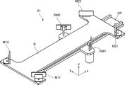
- FIG. 3 is an enlarged perspective view of an optical path length adjustment unit 21.
- FIG. 5 is a plan view showing the operation of the optical path length adjustment unit 21.
- FIG. 1 is a cross-sectional view showing an example of an organic EL display.
- the organic EL display shown in FIG. 1 is an active matrix type display device in which a TFT is disposed in each pixel PX.
- the organic EL display includes a film 218, a release layer 212, a TFT (Thin Film Transistor) layer 311, an organic layer 312, a color filter layer 313, and a protective layer 214.
- FIG. 1 shows a top emission type organic EL display in which the protective layer 214 side is the viewing side.
- the following description shows one configuration example of the organic EL display, and the present embodiment is not limited to the configuration described below. For example, in the present embodiment, it may be used for a bottom emission type organic EL display.
- the film 218 is a plastic film and can be bent by applying stress.
- a release layer 212 and a TFT layer 311 are provided over the film 218.
- the TFT layer 311 includes a TFT 311a disposed in each pixel PX. Further, the TFT layer 311 has wiring (not shown) connected to the TFT 311a.
- the TFT 311a, wiring, and the like constitute a pixel circuit.
- the organic layer 312 has an organic EL light emitting element 312a arranged for each pixel PX.
- the organic EL light emitting element 312a has, for example, a stacked structure in which an anode, a hole injection layer, a hole transport layer, a light emitting layer, an electron transport layer, an electron injection layer, and a cathode are stacked.
- the anode is a metal electrode
- the cathode is a transparent conductive film such as ITO (Indium Tin Oxide).
- the organic layer 312 is provided with a partition 312b for separating the organic EL light emitting element 312a between the pixels PX.
- a color filter layer 313 is provided on the organic layer 312.
- the color filter layer 313 is provided with a color filter 313a for performing color display. That is, each pixel PX is provided with a resin layer colored in R (red), G (green), or B (blue) as the color filter 313a.
- R red
- G green
- B blue
- the color filter layer 313 may be omitted in the case of a three-color system in which the organic layer 312 is provided with organic EL light-emitting elements that emit RGB colors.
- a protective layer 214 is provided on the color filter layer 313.
- the protective layer 214 is made of a resin material, and is provided to prevent deterioration of the organic EL light emitting element of the organic layer 312.
- the current flowing through the organic EL light emitting element 312a of the organic layer 312 varies depending on the display signal supplied to the pixel circuit. Therefore, the amount of light emitted from each pixel PX can be controlled by supplying a display signal corresponding to the display image to each pixel PX. Thereby, a desired image can be displayed.
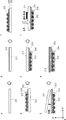
- FIG. 2 is a cross-sectional flowchart showing an outline of the manufacturing process of the organic EL display.
- a substrate 211 is prepared (step A).
- a glass substrate that transmits a laser beam is used as the substrate 211.
- the peeling layer 212 is formed on the substrate 211 (step B).
- the release layer 212 for example, polyimide can be used.
- the circuit element 213 is formed on the peeling layer 212 (process C).
- the circuit element 213 includes the TFT layer 311, the organic layer 312, and the color filter layer 313 shown in FIG. 1.
- the circuit element 213 can be formed using a photolithography technique or a film formation technique.
- a protective layer 214 for protecting the circuit element 213 is formed on the circuit element 213 (step D).
- the substrate 211 is turned over so that the substrate 211 faces upward (step E), and the release layer 212 is irradiated with the laser beam LB from the substrate 211 side (step F).
- a square beam can be used as the laser beam LB.
- the laser beam LB is irradiated from the right side to the left side of the substrate 211.
- the substrate 211 and the release layer 212 are separated (step G).
- the film 218 is laminated on the release layer 212 (Step H).
- the film 218 is a plastic film and can be bent by applying stress. By using such a manufacturing process, a bendable organic EL display can be manufactured.
- FIG. 3 is a schematic side view of a laser peeling device (laser lift-off device).
- the laser peeling apparatus 100 includes a laser light source 10, an optical system 20, and a stage 30.
- a laser beam LB is supplied from the laser light source 10 to the optical system 20.
- the laser light source 10 for example, a pulse laser generator that generates an excimer laser or an ultraviolet (UV) laser can be used.
- the optical system 20 includes a lens and a mirror.
- the stage 30 is a transporter that transports the workpiece 210 arranged on the stage 30 in the transport direction (x-axis direction). For example, the stage 30 injects gas upward from the upper surface and conveys the plate-like workpiece 210 while floating horizontally.
- the workpiece 210 includes at least a substrate 211 and a release layer 212. Note that illustration of circuit elements and the like formed on the peeling layer 212 is omitted.
- the workpiece 210 is arranged on the stage 30 so that the substrate 211 is on the upper side so that the laser beam LB is irradiated from the substrate 211 side to the interface between the substrate 211 and the peeling layer 212. Further, the stage 30 is configured to be movable in the vertical direction (direction along the z axis) so that the focal point of the laser beam LB is aligned with the interface between the substrate 211 and the release layer 212.
- the stage 30 while irradiating the laser beam LB, the stage 30 is moved in the transport direction (x-axis direction) and the work 210 is transported in the transport direction, thereby scanning the laser beam LB on the work 210. be able to.
- irradiation with the laser beam LB decomposes atomic / molecular bonds in the vicinity of the interface between the substrate 211 and the separation layer 212, so that the substrate 211 and the separation layer 212 can be separated at the interface.
- FIG. 4 is a plan view showing the shape of a laser spot in the laser peeling apparatus according to the comparative example.
- a linear laser beam LB with a fixed irradiation position is irradiated while the workpiece 210 is conveyed in the x-axis direction. Since the laser beam LB is pulse-oscillated, a linear laser spot LS is intermittently formed on the workpiece 210 while moving in the negative x-axis direction.
- an example of the dimension of the line-shaped laser spot LS has a major axis width L of 750 mm and a minor axis width S of 0.39 mm.
- the laser spots LS are overlapped by 50% in the minor axis direction (x-axis direction). That is, the substrate 211 and the peeling layer 212 in the workpiece 210 are peeled off by irradiating the laser spot LS twice.
- the laser spot LS in the laser peeling apparatus according to the comparative example has a large major axis width L and a ratio L / S of the major axis width L to the minor axis width S. Therefore, there is a problem that the lens system for forming the laser spot LS becomes larger and longer.
- the short axis width S of the laser spot LS in the laser peeling apparatus according to the comparative example is small. Therefore, there is a problem that the overlap ratio of the laser spot LS is likely to vary, and the substrate 211 and the peeling layer 212 are not peeled in a region where the predetermined number of irradiation times (two times in the example of FIG. 4) is not reached.
- FIG. 5 is a graph showing intensity profiles in the major axis direction and the minor axis direction of the laser spot LS in the laser peeling apparatus according to the comparative example.
- the major axis width L of the laser spot LS is a section where the intensity is constant, and has rising and falling inclined portions at both ends of the section.
- the major axis width L is 750 mm, while the width W1 of the inclined portion is 17.5 mm.
- the laser spot LS in the laser peeling apparatus according to the comparative example has a large long axis width L, and thus the width of the inclined portion in the long axis direction also increases. Therefore, when the laser spots LS are adjacently connected in the long axis direction, the laser beam LS is adjacent to each other in the long axis direction, and the inclined portions overlap each other, and the irradiated laser intensity becomes unstable. there were.
- the minor axis width S is 0.39 mm
- the width W2 of the inclined portion is 0.09 mm. That is, since the width of the inclined portion in the minor axis direction is extremely small, such a problem does not occur.
- FIG. 6 is a plan view showing the shape of a laser spot in the laser peeling apparatus according to Embodiment 1.
- FIG. 6 the shape of the laser spot LS on the workpiece 210 of the laser beam LB irradiated from the laser peeling apparatus according to the first embodiment is a square shape.
- the laser beam LB having a square laser spot LS is irradiated while being repeatedly scanned in the y-axis direction. Since the laser beam LB is pulse-oscillated, the line-shaped laser spot LS is intermittently formed on the workpiece 210 while moving in the negative y-axis direction.
- the laser beam LB is scanned in the negative y-axis direction, then moved in the negative x-axis direction, scanned in the positive y-axis direction, and then moved in the negative x-axis direction.
- the laser spots LS are not overlapped in the major axis direction (x-axis direction) but are overlapped by 50% in the minor axis direction (y-axis direction). That is, the substrate 211 and the peeling layer 212 in the workpiece 210 are peeled off by irradiating the laser spot LS twice.
- the long axis width L of the rectangular laser spot LS is 10 to 200 mm (that is, 10 mm ⁇ L ⁇ 200 mm), and the ratio L / S of the long axis width L to the short axis width S is 20 or less (that is, L / S ⁇ 20). If L> 200 mm or L / S> 20, the lens system for forming the laser spot LS will be enlarged and lengthened. On the other hand, when L ⁇ 10 mm, the number of scans of the laser beam LB increases, and the productivity decreases.
- the laser spot LS in the laser peeling apparatus according to Embodiment 1 has a long axis width L of 200 mm or less and a ratio L / S of the long axis width L to the short axis width S of 1 to 20, so that the lens system has a large size. Can be suppressed. Moreover, since the major axis width L is 10 mm or more, it is excellent in productivity.
- the width of the inclined portion in the major axis direction is preferably 0.1 mm or less.
- the width of the inclined portion may be further reduced by providing a slit through which the laser beam LB formed by the lens system passes.
- the short axis width S of the rectangular laser spot LS is 2 to 30 mm (that is, 2 mm ⁇ S ⁇ 30 mm).
- S ⁇ 2 mm the overlap rate of the laser spot LS tends to vary. Therefore, the substrate 211 and the release layer 212 in the workpiece 210 are not peeled in a region that does not reach the predetermined number of times of irradiation (twice in the example of FIG. 6).
- S> 30 mm the area of the laser spot LS becomes too large, and it becomes difficult to obtain the laser intensity necessary for peeling.
- the short axis width S of the laser spot LS in the laser peeling apparatus according to Embodiment 1 is 2 mm or more, unpeeling of the substrate 211 and the peeling layer 212 in the workpiece 210 can be suppressed. Further, since the minor axis width S is 30 mm or less, sufficient laser intensity necessary for peeling can be obtained.
- the overlap rate of the laser spot LS is 50% of 2 times irradiation, 67% of 3 times irradiation, 75% of 4 times irradiation, 80% of 5 times irradiation, 90% of 10 times irradiation, 20 times irradiation 95% or the like may be adopted.
- the overlap rate exceeds 80%, the number of irradiations increases too much, and the productivity decreases. That is, the overlap rate is preferably 50 to 80%.
- FIG. 7 is also a plan view showing the shape of the laser spot in the laser peeling apparatus according to the first embodiment.
- the shape of the laser spot LS shown in FIG. 7 is the same as the shape of the laser spot LS shown in FIG.
- the laser beam LB having a square laser spot LS is irradiated while being repeatedly scanned in the x-axis direction. Since the laser beam LB is pulse-oscillated, a linear laser spot LS is intermittently formed on the workpiece 210 while moving in the negative x-axis direction.
- the laser beam LB is scanned in the negative x-axis direction, then moved in the negative y-axis direction, scanned in the positive x-axis direction, and then moved in the negative y-axis direction.
- the laser spots LS are not overlapped in the minor axis direction (y-axis direction) but are overlapped by 50% in the major axis direction (x-axis direction). That is, the substrate 211 and the peeling layer 212 in the workpiece 210 are peeled off by irradiating the laser spot LS twice.
- the laser spot LS may overlap in the minor axis direction, or the laser spot LS may overlap in the major axis direction.
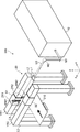
- FIG. 8 is a perspective view of the laser peeling apparatus according to the second embodiment.
- the laser peeling apparatus 200 according to the second embodiment also includes the laser light source 10, the optical system 20, and the stage 30, but in FIG. The stage 30 is omitted.
- the optical system 20 includes mirrors M1 and M2, molded lenses L1 and L2, and movable mirrors MM1 and MM2.
- the laser beam LB emitted from the laser light source 10 in the negative x-axis direction is reflected by the mirror M1, travels in the positive z-axis direction, and then is reflected by the mirror M2 in the positive y-axis direction. proceed.
- the laser beam LB emitted from the laser light source 10 is parallel light having a square cross section.
- the laser beam LB reflected by the mirror M2 is expanded in the x-axis direction by the shaping lens L1, and then converted into parallel light again by the shaping lens L2.
- the molded lenses L1 and L2 are, for example, cylindrical lenses.
- the laser beam LB formed by the forming lenses L1 and L2 is reflected by one of the movable mirrors MM1 and MM2, travels in the negative z-axis direction, and is irradiated onto the workpiece 210. At this time, the workpiece 210 is conveyed in the x-axis positive direction.
- the movable mirror MM1 is mounted on a slider S1 that slides on a y-axis rail YR1 extending in the y-axis direction. That is, the movable mirror MM1 can move in the y-axis direction.
- the y-axis rail YR1 is provided in parallel with the y-axis rail YR2, and the movable mirror MM1 is provided so as to protrude from the y-axis rail YR1 toward the y-axis rail YR2, that is, in the negative x-axis direction.
- a pair of columns C1 that support the y-axis rail YR1 are provided at both ends of the y-axis rail YR1.
- the movable mirror MM1 is mounted on a z-axis rail ZR1 fixed to the slider S1, and can also move in the z-axis direction.
- the movable mirror MM2 is mounted on a slider S2 that slides on a y-axis rail YR2 extending in the y-axis direction. That is, the movable mirror MM2 can move in the y-axis direction.
- the movable mirror MM2 is provided so as to protrude from the y-axis rail YR2 toward the y-axis rail YR1, that is, in the positive x-axis direction.
- a pair of support columns C2 that support the y-axis rail YR2 are provided.
- the movable mirror MM2 is mounted on a z-axis rail ZR2 fixed to the slider S2, and can also move in the z-axis direction.
- FIG. 9 is a side view showing the configuration and operation of the movable mirror MM1.
- FIG. 10 is a front view showing the configuration and operation of the movable mirrors MM1 and MM2.
- the upper part of FIG. 9 corresponds to the upper part of FIG. 10
- the lower part of FIG. 9 corresponds to the lower part of FIG.
- the movable mirror MM1 reflects the laser beam LB traveling in the positive y-axis direction in the negative z-axis direction while moving in the negative y-axis direction. That is, when the movable mirror MM1 moves in the y-axis negative direction along the incident optical axis of the laser beam LB, the laser beam LB reflected by the movable mirror MM1 is also scanned in the y-axis negative direction by the workpiece 210.
- the stroke ST1 of the movable mirror MM1 is approximately the same as the width (length in the y-axis direction) of the workpiece 210.
- the incident optical axis of the laser beam LB is parallel to the main surface of the substrate 211 of the workpiece 210 and perpendicular to the conveyance direction (x-axis direction) of the workpiece 210.
- the movable mirror MM1 when the movable mirror MM1 reaches the end on the y-axis negative direction side of the y-axis rail YR1, it moves in the z-axis positive direction along the z-axis rail ZR1 as shown in the lower part of FIG. 9 and the lower part of FIG. To do.
- the laser beam LB is irradiated by the movable mirror MM2 standing by at the y-axis positive direction end of the y-axis rail YR2 (not shown in FIG. 9).
- the movable mirror MM2 In the lower part of FIG. 9, the movable mirror MM2 is shown for easy understanding.
- the movable mirror MM1 moves in the y-axis positive direction without reflecting the laser beam LB.
- the movable mirror MM1 reaches the end on the y-axis positive direction side of the y-axis rail YR1, it moves in the z-axis negative direction along the z-axis rail ZR1 and stands by.
- the movable mirror MM2 reflects the laser beam LB traveling in the positive y-axis direction in the negative z-axis direction while moving in the negative y-axis direction.
- laser beam LB reflected by movable mirror MM2 is also scanned in negative y-axis direction at workpiece 210.
- the stroke of the movable mirror MM2 is the same as the stroke ST1 of the movable mirror MM1.
- the movable mirror MM2 moves in the z-axis positive direction along the z-axis rail ZR2 as shown in the upper part of FIG.
- the laser beam LB is applied to the movable mirror MM1 waiting at the end on the y-axis positive direction side of the y-axis rail YR1.
- the movable mirrors MM1 and MM2 alternately repeat the operations shown in the upper part of FIG. 9 and the upper part of FIG. 10 and the operations shown in the lower part of FIG. 9 and the lower part of FIG. That is, the movable mirrors MM1 and MM2 reflect the laser beam LB traveling in the positive y-axis direction in the negative z-axis direction while alternately moving in the negative y-axis direction.
- the entire surface of the workpiece 210 can be irradiated with the laser beam LB while the workpiece 210 is conveyed at a constant speed.
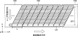
- FIG. 11 is a plan view showing a laser spot LS irradiated by the laser peeling apparatus according to the second embodiment.
- the laser beam LB is scanned in the negative y-axis direction while the workpiece 210 is conveyed in the positive x-axis direction at a constant speed. Therefore, the laser spots LS are sequentially formed in the negative y-axis direction while being shifted in the negative x-axis direction in each column, as indicated by solid arrows.
- the moving distance in the y-axis direction of the laser spot LS shown in FIG. 11 is equal to the moving distance in the y-axis direction of the movable mirror MM1 shown in FIG. 9 (ie, the stroke ST1).
- the workpiece 210 is conveyed by the long axis width L.
- the moving speed of the movable mirrors MM1 and MM2 can be set by the pulse frequency of the laser beam LB and the overlap rate of the laser spot LS.
- work 210 can be set from the moving speed of movable mirror MM1, MM2.
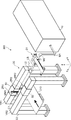
- FIG. 12 is a perspective view of the laser peeling apparatus according to the third embodiment.
- the laser peeling apparatus 300 according to the third embodiment includes an optical path length adjustment unit 21 in addition to the configuration of the laser peeling apparatus 200 according to the second embodiment shown in FIG.
- the optical path length adjustment unit 21 cancels the change in the optical path length of the laser beam LB due to the movement of the movable mirrors MM1 and MM2, and adjusts the optical path length of the laser beam LB to be constant.
- the movable mirrors MM1 and MM2 reflect the laser beam LB traveling in the positive y-axis direction in the negative z-axis direction while moving in the negative y-axis direction. Therefore, the optical path length of the laser beam LB becomes shorter as the movable mirrors MM1 and MM2 move in the negative y-axis direction.
- the optical path length of the laser beam LB is kept constant by the optical path length adjustment unit 21 even when the movable mirrors MM1 and MM2 move in the negative y-axis direction. be able to.
- the optical path length adjustment unit 21 is provided between the mirror M2 and the molded lens L1.
- the installation position of the optical path length adjustment unit 21 is not particularly limited as long as it is on the path of the laser beam LB.
- the configuration other than the optical path length adjusting unit 21 is the same as that of the laser peeling apparatus 200 according to the second embodiment shown in FIG. Description is omitted.
- FIG. 13 is an enlarged perspective view of the optical path length adjustment unit 21.
- the optical path length adjustment unit 21 includes an x-axis rail XR, a base B, four fixed mirrors M11, M12, M21, and M22, and two rotary mirrors RM1 and RM2.
- the x-axis rail XR is a rail extending in the x-axis direction.
- the x-axis rail XR has a protruding portion that protrudes on both sides in the y-axis direction at the central portion in the x-axis negative direction.
- the rotating mirror RM1 is fixed to the protruding portion protruding in the negative y-axis direction so as to be rotatable about the z-axis
- the rotating mirror RM2 is fixed to the protruding portion protruding in the positive y-axis direction so as to be rotatable about the z-axis. ing.
- the base B is a plate-like member having an I-shape in plan view that extends in the x-axis direction, and is placed on the x-axis rail XR so as to be slidable in the x-axis direction.
- the fixed mirror M11 is fixed to the protrusion protruding in the y-axis negative direction
- the fixed mirror M12 is fixed to the protrusion protruding in the y-axis positive direction.
- the fixed mirror M21 is fixed to the protruding part protruding in the negative y-axis direction
- the fixed mirror M22 is fixed to the protruding part protruding in the positive y-axis direction.
- the laser beam LB traveling in the positive y-axis direction is incident on the rotating mirror RM1 and passes through the fixed mirrors M11 and M12 or the fixed mirrors M21 and M22.
- the light is emitted from the rotating mirror RM2 in the positive y-axis direction.
- the laser beam LB passes through the fixed mirrors M21 and M22 (see FIG. 13).
- the laser beam LB is reflected by the rotating mirror RM1 and travels in the positive x-axis direction or the positive x-axis direction. Since the rotating mirror RM1 is rotatable, the laser beam LB traveling in the y-axis positive direction can be reflected in the x-axis positive direction or the x-axis positive direction. In FIG. 12, the laser beam LB is reflected by the rotating mirror RM1 and travels in the positive x-axis direction.
- the laser beam LB traveling in the positive x-axis direction is reflected by the fixed mirror M21, travels in the positive y-axis direction, reflected by the fixed mirror M22, and negative in the x-axis. After traveling in the direction, the light enters the rotating mirror RM2. Then, the laser beam LB is reflected by the rotating mirror RM2 and travels in the positive y-axis direction.
- the base B can slide on the x-axis rail XR in the x-axis direction, the distance between the rotating mirror RM1 and the fixed mirror M21 and the distance between the rotating mirror RM2 and the fixed mirror M22. The distance can be changed.
- the rotating mirrors RM1 and RM2 and the fixed mirrors M21 and M22 move away from each other.
- the optical path length at 21 is increased.
- the rotating mirrors RM1 and RM2 and the fixed mirrors M21 and M22 approach each other, so that the optical path length in the optical path length adjustment unit 21 is shortened.
- the laser beam LB when the laser beam LB is reflected by the rotating mirror RM1 and travels in the x-axis negative direction, the laser beam LB is reflected by the fixed mirror M11 and travels in the y-axis positive direction, and is reflected by the fixed mirror M12 and x After traveling in the positive axial direction, the light enters the rotating mirror RM2. Then, the laser beam LB is reflected by the rotating mirror RM2 and travels in the positive y-axis direction. Since the rotating mirror RM2 is rotatable, the laser beam LB traveling in the positive x-axis direction and the laser beam LB traveling in the negative x-axis direction as shown in FIG. 12 are reflected in the positive y-axis direction. can do.
- the base B can slide on the x-axis rail XR in the x-axis direction, the distance between the rotating mirror RM1 and the fixed mirror M11, and the distance between the rotating mirror RM2 and the fixed mirror M12. The distance can be changed.
- the rotation mirrors RM1 and RM2 and the fixed mirrors M11 and M12 move away when the base B moves in the negative x-axis direction.
- the optical path length at 21 is increased.
- the rotating mirrors RM1 and RM2 and the fixed mirrors M11 and M12 approach each other, so that the optical path length in the optical path length adjustment unit 21 is shortened.
- FIG. 14 is a plan view showing the operation of the optical path length adjustment unit 21.
- the optical path length adjustment unit 21 operates in synchronization with the operations of the movable mirrors MM1 and MM2 described with reference to FIGS. That is, the base B moves in the x-axis direction in synchronization with the movement of the movable mirrors MM1 and MM2 in the negative y-axis direction so that the optical path length of the laser beam LB is kept constant. Details of the operation of the optical path length adjustment unit 21 will be described below with reference to FIG. 9 together with FIG.
- the movable mirror MM1 starts reflecting the laser beam LB at the y-axis positive direction end of the y-axis rail YR1, as shown on the leftmost side of FIG. Is located closest to the positive x-axis direction.
- the laser beam LB incident on the rotating mirror RM1 is emitted from the rotating mirror RM2 via the fixed mirrors M11 and M12. Since the base B is located closest to the positive x-axis direction, the rotating mirrors RM1 and RM2 and the fixed mirrors M11 and M12 are closest to each other, and the optical path length in the optical path length adjustment unit 21 is the shortest.
- the base B when the movable mirror MM1 moves forward in the negative y-axis direction, the base B also moves in the negative x-axis direction synchronously as shown second from the left in FIG.
- the second state from the left in FIG. 14 is a state in which the base B has reached the x-axis negative direction side most. Therefore, the rotating mirrors RM1 and RM2 and the fixed mirrors M11 and M12 are farthest away, and the optical path length in the optical path length adjustment unit 21 is the longest.
- the stroke ST2 of the base B is set to 1 ⁇ 2 of the stroke ST1 of the movable mirror MM1 shown in FIG. 9, as shown in FIG. Further, the moving speed of the base B is also 1 ⁇ 2 of the moving speed of the movable mirror MM1.
- the irradiation target of the laser beam LB is switched from the movable mirror MM1 to the movable mirror MM2, as shown in the lower part of FIG. .
- the rotating mirrors RM1 and RM2 rotate in the second state from the left in FIG.
- the laser beam LB incident on the rotating mirror RM1 is switched so as to be emitted from the rotating mirror RM2 via the fixed mirrors M21 and M22.
- the base B does not move.
- the optical path length adjustment unit 21 is the shortest. That is, in the optical path length adjustment unit 21, the optical path length in the state shown on the left side in FIG. 14 is equal to the optical path length in the state shown third from the left in FIG.
- the base B when the movable mirror MM2 moves forward in the negative y-axis direction, the base B also moves in the positive x-axis direction synchronously as shown on the rightmost side of FIG.
- the state shown on the rightmost side of FIG. 14 is a state in which the base B has reached the x axis positive direction side most. Therefore, the rotation mirrors RM1 and RM2 and the fixed mirrors M21 and M22 are farthest away, and the optical path length in the optical path length adjustment unit 21 is the longest. That is, in the optical path length adjustment unit 21, the optical path length in the second state in FIG. 14 is equal to the optical path length in the rightmost state in FIG.
- the irradiation target of the laser beam LB is switched from the movable mirror MM2 to the movable mirror MM1, as shown in the upper part of FIG. .
- the rotating mirrors RM1 and RM2 rotate in the state shown on the rightmost side of FIG. Accordingly, the state shown in the leftmost side of FIG. 14 is restored, and the laser beam LB incident on the rotating mirror RM1 is switched to be emitted from the rotating mirror RM2 via the fixed mirrors M11 and M12.
- the base B does not move.
- the optical path length adjustment unit 21 repeats the above operation, so that the optical path length of the laser beam LB can always be kept constant even when the movable mirrors MM1 and MM2 are sequentially moved in the negative y-axis direction.
Landscapes
- Engineering & Computer Science (AREA)
- Physics & Mathematics (AREA)
- Optics & Photonics (AREA)
- Mechanical Engineering (AREA)
- Plasma & Fusion (AREA)
- Chemical & Material Sciences (AREA)
- Chemical Kinetics & Catalysis (AREA)
- General Chemical & Material Sciences (AREA)
- Oil, Petroleum & Natural Gas (AREA)
- Manufacturing & Machinery (AREA)
- General Physics & Mathematics (AREA)
- Theoretical Computer Science (AREA)
- Laser Beam Processing (AREA)
- Electroluminescent Light Sources (AREA)
- Devices For Indicating Variable Information By Combining Individual Elements (AREA)
Abstract
一実施の形態に係るレーザ剥離装置(100)は、基板(211)と当該基板上に形成された剥離層(212)とを備えるワーク(210)にレーザビーム(LB)を照射して剥離層(212)を基板(211)から剥離するものである。ワーク(210)に照射されるレーザビーム(LB)のスポット(LS)が方形状であり、スポット(LS)の長軸幅Lが10~200mmであり、スポット(LS)の短軸幅Sが2~30mmであり、スポット(LS)の短軸幅Sに対する長軸幅Lの比L/Sが1~20である。
Description
本発明はレーザ剥離装置、レーザ剥離方法、及び有機ELディスプレイの製造方法に関し、例えばレーザビームを用いて基板から剥離層を分離するレーザ剥離装置、レーザ剥離方法、及び有機ELディスプレイの製造方法に関する。
基板上に形成された剥離層に、基板側からレーザビームを照射して剥離層を基板から剥離するレーザ剥離装置が知られている。特許文献1には、線状のレーザスポットを連続的に照射して基板から剥離層を剥離するレーザ剥離装置が開示されている。
発明者は、レーザスポットを連続的に照射して基板から剥離層を剥離するレーザ剥離装置の開発に際し、レーザスポットの形状及び寸法について様々な課題を見出した。
その他の課題と新規な特徴は、本明細書の記述及び添付図面から明らかになるであろう。
その他の課題と新規な特徴は、本明細書の記述及び添付図面から明らかになるであろう。
一実施の形態に係るレーザ剥離装置は、ワークに照射されるレーザビームのスポットが方形状であり、スポットの長軸幅Lが10~200mmであり、スポットの短軸幅Sが2~30mmであり、スポットの短軸幅Sに対する長軸幅Lの比L/Sが1~20である。
一実施の形態に係るレーザ剥離方法は、ワークに照射されるレーザビームのスポットが方形状であり、スポットの長軸幅Lが10~200mmであり、スポットの短軸幅Sが2~30mmであり、スポットの短軸幅Sに対する長軸幅Lの比L/Sが1~20である。
一実施の形態に係る有機ELディスプレイの製造方法は、剥離層を基板から剥離する工程において、ワークに照射されるレーザビームのスポットが方形状であり、スポットの長軸幅Lが10~200mmであり、スポットの短軸幅Sが2~30mmであり、スポットの短軸幅Sに対する長軸幅Lの比L/Sが1~20である。
前記一実施の形態によれば、優れたレーザ剥離装置、レーザ剥離方法、及び有機ELディスプレイの製造方法を提供することができる。
以下、具体的な実施の形態について、図面を参照しながら詳細に説明する。ただし、以下の実施の形態に限定される訳ではない。また、説明を明確にするため、以下の記載及び図面は、適宜簡略化されている。
(実施の形態1)
<有機ELディスプレイ>
まず、図1を参照して、実施の形態1に係る有機EL(Electroluminescence)ディスプレイの製造方法を用いて製造される有機ELディスプレイの構造について説明する。図1は、有機ELディスプレイの一例を示す断面図である。図1に示す有機ELディスプレイは、各画素PXにTFTが配置されたアクティブマトリクス型の表示装置である。
<有機ELディスプレイ>
まず、図1を参照して、実施の形態1に係る有機EL(Electroluminescence)ディスプレイの製造方法を用いて製造される有機ELディスプレイの構造について説明する。図1は、有機ELディスプレイの一例を示す断面図である。図1に示す有機ELディスプレイは、各画素PXにTFTが配置されたアクティブマトリクス型の表示装置である。
有機ELディスプレイは、フィルム218、剥離層212、TFT(Thin Film Transistor)層311、有機層312、カラーフィルタ層313、及び保護層214を備えている。図1では、保護層214側が視認側となるトップエミッション方式の有機ELディスプレイを示している。なお、以下の説明は、有機ELディスプレイの一構成例を示すものであり、本実施の形態は、以下に説明される構成に限られるものではない。例えば、本実施の形態では、ボトムエミッション方式の有機ELディスプレイに用いられてもよい。
フィルム218は、プラスチックフィルムであり、応力を加えることにより曲げることができる。フィルム218の上には、剥離層212、TFT層311が設けられている。TFT層311は、各画素PXに配置されたTFT311aを有している。さらに、TFT層311は、TFT311aに接続される配線(不図示)等を有している。TFT311a、及び配線等が画素回路を構成する。
TFT層311の上には、有機層312が設けられている。有機層312は、画素PXごとに配置された有機EL発光素子312aを有している。有機EL発光素子312aは、例えば、陽極、正孔注入層、正孔輸送層、発光層、電子輸送層、電子注入層、及び陰極が積層された積層構造を有している。トップエミッション方式の場合、陽極は金属電極であり、陰極はITO(Indium Tin Oxide)等の透明導電膜である。さらに、有機層312には、画素PX間において、有機EL発光素子312aを分離するための隔壁312bが設けられている。
有機層312の上には、カラーフィルタ層313が設けられている。カラーフィルタ層313は、カラー表示を行うためのカラーフィルタ313aが設けられている。すなわち、各画素PXには、R(赤色)、G(緑色)、又はB(青色)に着色された樹脂層がカラーフィルタ313aとして設けられている。有機層312から放出された白色光は、カラーフィルタ313aを通過すると、RGBの色の光に変換される。なお、有機層312に、RGBの各色を発光する有機EL発光素子が設けられている3色方式の場合、カラーフィルタ層313を省略してもよい。
カラーフィルタ層313の上には、保護層214が設けられている。保護層214は、樹脂材料で構成されており、有機層312の有機EL発光素子の劣化を防ぐために設けられている。
有機層312の有機EL発光素子312aに流れる電流は、画素回路に供給される表示信号によって変化する。よって、表示画像に応じた表示信号を各画素PXに供給することで、各画素PXでの発光量を制御することができる。これにより、所望の画像を表示することができる。
<有機ELディスプレイの製造工程>
次に、図2を参照して、実施の形態1に係る有機ELディスプレイの製造方法の概要について説明する。図2は、有機ELディスプレイの製造工程の概要を示す断面フロー図である。
次に、図2を参照して、実施の形態1に係る有機ELディスプレイの製造方法の概要について説明する。図2は、有機ELディスプレイの製造工程の概要を示す断面フロー図である。
なお、当然のことながら、図2及びその他の図面に示した右手系xyz座標は、構成要素の位置関係を説明するための便宜的なものである。通常、z軸プラス向きが鉛直上向き、xy平面が水平面であり、図面間で共通である。
有機ELディスプレイを製造する際は、まず基板211を準備する(工程A)。例えば、基板211にはレーザビームを透過するガラス基板を用いる。
次に、基板211の上に剥離層212を形成する(工程B)。剥離層212には、例えばポリイミドを用いることができる。
次に、基板211の上に剥離層212を形成する(工程B)。剥離層212には、例えばポリイミドを用いることができる。
その後、剥離層212の上に回路素子213を形成する(工程C)。ここで、回路素子213は、図1に示すTFT層311、有機層312、カラーフィルタ層313を含む。回路素子213は、フォトリソグラフィ技術や成膜技術を用いて形成することができる。
その後、回路素子213の上に、回路素子213を保護するための保護層214を形成する(工程D)。
その後、回路素子213の上に、回路素子213を保護するための保護層214を形成する(工程D)。
次に、基板211が上になるように基板211を反転させ(工程E)、基板211側から剥離層212にレーザビームLBを照射する(工程F)。レーザビームLBには方形ビームを用いることができる。図2に示す場合は、基板211をx方向に搬送しているので、基板211の右側から左側に向かってレーザビームLBが照射される。
その後、基板211と剥離層212とを分離する(工程G)。
最後に、フィルム218を剥離層212に積層する(工程H)。例えば、フィルム218はプラスチックフィルムであり、応力を加えることにより曲げることができるフィルムである。このような製造工程を用いることで、折り曲げ可能な有機ELディスプレイを製造することができる。
最後に、フィルム218を剥離層212に積層する(工程H)。例えば、フィルム218はプラスチックフィルムであり、応力を加えることにより曲げることができるフィルムである。このような製造工程を用いることで、折り曲げ可能な有機ELディスプレイを製造することができる。
<レーザ剥離装置の基本構成>
次に、図3を参照して、工程Fで用いられる実施の形態1に係るレーザ剥離装置の基本構成について説明する。図3は、レーザ剥離装置(レーザリフトオフ装置)の模式的側面図である。図3に示すように、レーザ剥離装置100は、レーザ光源10、光学系20、及びステージ30を備える。光学系20には、レーザ光源10からレーザビームLBが供給される。レーザ光源10には、例えばエキシマレーザや紫外(UV)レーザを発生させるパルスレーザ発生装置を用いることができる。光学系20はレンズやミラーから構成されている。
次に、図3を参照して、工程Fで用いられる実施の形態1に係るレーザ剥離装置の基本構成について説明する。図3は、レーザ剥離装置(レーザリフトオフ装置)の模式的側面図である。図3に示すように、レーザ剥離装置100は、レーザ光源10、光学系20、及びステージ30を備える。光学系20には、レーザ光源10からレーザビームLBが供給される。レーザ光源10には、例えばエキシマレーザや紫外(UV)レーザを発生させるパルスレーザ発生装置を用いることができる。光学系20はレンズやミラーから構成されている。
ステージ30は、ステージ30上に配置されたワーク210を搬送方向(x軸方向)に搬送する搬送機である。例えば、ステージ30は、上面から上向きにガスを噴射して、板状のワーク210を水平に浮上させながら搬送する。ここで、ワーク210は少なくとも基板211と剥離層212とを備える。なお、剥離層212の上に形成されている回路素子等は図示を省略している。ワーク210は、基板211側から基板211と剥離層212との界面にレーザビームLBが照射されるように、基板211が上側になるようにステージ30上に配置されている。また、ステージ30は、レーザビームLBの焦点が基板211と剥離層212との界面に合うように上下方向(z軸に沿った方向)に移動可能に構成されている。
図3に示すように、レーザビームLBを照射しながら、ステージ30を搬送方向(x軸方向)に移動させてワーク210を搬送方向に搬送することで、ワーク210上においてレーザビームLBを走査することができる。このとき、レーザビームLBが照射されることで、基板211と剥離層212との界面付近において原子・分子の結合が分解するため、基板211と剥離層212とを界面において分離することができる。
<実施の形態1の比較例に係るレーザ剥離装置でのレーザスポット>
次に、図4を参照して、実施の形態1の比較例に係るレーザ剥離装置でのレーザスポットの形状について説明する。図4は、比較例に係るレーザ剥離装置でのレーザスポットの形状を示す平面図である。図4に示すように、ワーク210をx軸方向に搬送しながら、照射位置が固定されたライン状のレーザビームLBを照射する。レーザビームLBはパルス発振されているため、ワーク210上においてライン状のレーザスポットLSがx軸負方向に移動しながら間欠的に形成されていく。
次に、図4を参照して、実施の形態1の比較例に係るレーザ剥離装置でのレーザスポットの形状について説明する。図4は、比較例に係るレーザ剥離装置でのレーザスポットの形状を示す平面図である。図4に示すように、ワーク210をx軸方向に搬送しながら、照射位置が固定されたライン状のレーザビームLBを照射する。レーザビームLBはパルス発振されているため、ワーク210上においてライン状のレーザスポットLSがx軸負方向に移動しながら間欠的に形成されていく。
ライン状のレーザスポットLSの寸法の一例は、図4に示すように、長軸幅Lは750mm、短軸幅Sは0.39mmである。図4の例では、レーザスポットLSを短軸方向(x軸方向)において50%ずつオーバーラップさせている。すなわち、レーザスポットLSを2回照射することによって、ワーク210における基板211と剥離層212とを剥離する。
ここで、比較例に係るレーザ剥離装置でのレーザスポットLSは、長軸幅Lと短軸幅Sに対する長軸幅Lの比L/Sとのいずれもが大きい。そのため、レーザスポットLSを成形するためのレンズ系が大型化・長大化してしまう問題があった。
他方、比較例に係るレーザ剥離装置でのレーザスポットLSは、短軸幅Sが小さい。そのため、レーザスポットLSのオーバーラップ率がばらつき易く、所定の照射回数(図4の例では2回)に達しない領域では、基板211と剥離層212とが未剥離となる問題があった。
他方、比較例に係るレーザ剥離装置でのレーザスポットLSは、短軸幅Sが小さい。そのため、レーザスポットLSのオーバーラップ率がばらつき易く、所定の照射回数(図4の例では2回)に達しない領域では、基板211と剥離層212とが未剥離となる問題があった。
さらに、レンズ系のさらなる大型化・長大化を抑制するために、レーザスポットLSを長軸方向にも隣接させて繋ぎ合わせる場合には、以下のような問題があった。
ここで、図5は、比較例に係るレーザ剥離装置でのレーザスポットLSの長軸方向及び短軸方向での強度プロファイルを示すグラフである。図5に示すように、レーザスポットLSの長軸幅Lは強度が一定の区間であり、その区間の両端に立ち上がり及び立ち下がりの傾斜部を有している。長軸方向では、一例として、長軸幅Lが750mmであるのに対し、傾斜部の幅W1は17.5mmであった。
ここで、図5は、比較例に係るレーザ剥離装置でのレーザスポットLSの長軸方向及び短軸方向での強度プロファイルを示すグラフである。図5に示すように、レーザスポットLSの長軸幅Lは強度が一定の区間であり、その区間の両端に立ち上がり及び立ち下がりの傾斜部を有している。長軸方向では、一例として、長軸幅Lが750mmであるのに対し、傾斜部の幅W1は17.5mmであった。
このように、比較例に係るレーザ剥離装置でのレーザスポットLSは、長軸幅Lが大きいため、長軸方向の傾斜部の幅も大きくなる。そのため、レーザスポットLSを長軸方向にも隣接させて繋ぎ合わせる場合、レーザスポットLS同士の長軸方向の隣接部では、傾斜部同士が重なり合い、照射されるレーザ強度が不安定になるという問題があった。
なお、図5に示すように、短軸方向では、一例として、短軸幅Sが0.39mmであるのに対し、傾斜部の幅W2は0.09mmであった。すなわち、短軸方向の傾斜部は、幅が極めて小さいため、このような問題は生じない。
なお、図5に示すように、短軸方向では、一例として、短軸幅Sが0.39mmであるのに対し、傾斜部の幅W2は0.09mmであった。すなわち、短軸方向の傾斜部は、幅が極めて小さいため、このような問題は生じない。
<実施の形態1に係るレーザ剥離装置でのレーザスポット>
次に、図6を参照して、実施の形態1に係るレーザ剥離装置でのレーザスポットの形状について説明する。図6は、実施の形態1に係るレーザ剥離装置でのレーザスポットの形状を示す平面図である。図6に示すように、実施の形態1に係るレーザ剥離装置から照射されるレーザビームLBのワーク210におけるレーザスポットLSの形状は方形状である。
次に、図6を参照して、実施の形態1に係るレーザ剥離装置でのレーザスポットの形状について説明する。図6は、実施の形態1に係るレーザ剥離装置でのレーザスポットの形状を示す平面図である。図6に示すように、実施の形態1に係るレーザ剥離装置から照射されるレーザビームLBのワーク210におけるレーザスポットLSの形状は方形状である。
図6に示すように、ワーク210の位置を固定した状態で、方形状のレーザスポットLSを有するレーザビームLBをy軸方向に繰り返し走査させながら照射する。レーザビームLBはパルス発振されているため、ワーク210上においてライン状のレーザスポットLSがy軸負方向に移動しながら間欠的に形成されていく。
図6の例では、レーザビームLBをy軸負方向に走査させた後、x軸負方向に移動し、y軸正方向に走査させた後、x軸負方向に移動することを繰り返している。図6の例では、レーザスポットLSを長軸方向(x軸方向)においてはオーバーラップさせずに、短軸方向(y軸方向)において50%ずつオーバーラップさせている。すなわち、レーザスポットLSを2回照射することによって、ワーク210における基板211と剥離層212とを剥離する。
ここで、方形状のレーザスポットLSの長軸幅Lは10~200mm(すなわち、10mm≦L≦200mm)であり、かつ短軸幅Sに対する長軸幅Lの比L/Sは20以下(すなわち、L/S≦20)を満たす。L>200mm、もしくは、L/S>20だと、レーザスポットLSを成形するためのレンズ系が大型化・長大化してしまう。他方、L<10mmだと、レーザビームLBの走査回数が増加し、生産性が低下する。ここで、短軸幅Sと長軸幅Lとが等しく、L/S=1であってもよい。すなわち、短軸幅Sに対する長軸幅Lの比L/Sは1~20(すなわち、1≦L/S≦20)である。
実施の形態1に係るレーザ剥離装置でのレーザスポットLSは、長軸幅Lが200mm以下かつ短軸幅Sに対する長軸幅Lの比L/Sが1~20であるため、レンズ系の大型化・長大化を抑制することができる。また、長軸幅Lが10mm以上であるため、生産性に優れている。
また、L≦200mmとすることによって、比較例よりも上述の長軸方向の傾斜部の幅を小さくすることができる。そのため、図6に示したレーザスポットLS同士の長軸方向の隣接部において、傾斜部同士が重なり合い、照射されるレーザ強度が不安定になることを抑制することができる。長軸方向の傾斜部の幅は、0.1mm以下であることが好ましい。
ここで、レンズ系によって成形されたレーザビームLBが通過するスリットを設けることによって、傾斜部の幅をさらに小さくしてもよい。
ここで、レンズ系によって成形されたレーザビームLBが通過するスリットを設けることによって、傾斜部の幅をさらに小さくしてもよい。
方形状のレーザスポットLSの短軸幅Sは2~30mm(すなわち、2mm≦S≦30mm)である。S<2mmだと、レーザスポットLSのオーバーラップ率がばらつき易くなる。そのため、所定の照射回数(図6の例では2回)に達しない領域では、ワーク210における基板211と剥離層212とが未剥離となる。他方、S>30mmだと、レーザスポットLSの面積が大きくなり過ぎ、剥離に必要なレーザ強度が得られ難くなる。
実施の形態1に係るレーザ剥離装置でのレーザスポットLSは、短軸幅Sが2mm以上であるため、ワーク210における基板211と剥離層212との未剥離を抑制することができる。また、短軸幅Sが30mm以下であるため、剥離に必要な充分なレーザ強度が得られる。
レーザスポットLSのオーバーラップ率は、2回照射の50%の他に、3回照射の67%、4回照射の75%、5回照射の80%、10回照射の90%、20回照射の95%などを採用してもよい。しかしながら、オーバーラップ率が80%を超えると、照射回数が多くなり過ぎ、生産性が低下する。すなわち、オーバーラップ率は50~80%であることが好ましい。
ここで、図7も、実施の形態1に係るレーザ剥離装置でのレーザスポットの形状を示す平面図である。図7に示したレーザスポットLSの形状は、図6に示したレーザスポットLSの形状と同じである。図7では、方形状のレーザスポットLSを有するレーザビームLBをx軸方向に繰り返し走査させながら照射する。レーザビームLBはパルス発振されているため、ワーク210上においてライン状のレーザスポットLSがx軸負方向に移動しながら間欠的に形成されていく。
図7の例では、レーザビームLBをx軸負方向に走査させた後、y軸負方向に移動し、x軸正方向に走査させた後、y軸負方向に移動することを繰り返している。図7の例では、レーザスポットLSを短軸方向(y軸方向)においてはオーバーラップさせずに、長軸方向(x軸方向)において50%ずつオーバーラップさせている。すなわち、レーザスポットLSを2回照射することによって、ワーク210における基板211と剥離層212とを剥離する。
図6、図7に示したように、レーザスポットLSを短軸方向にオーバーラップさせても、レーザスポットLSを長軸方向にオーバーラップさせてもよい。
図6、図7に示したように、レーザスポットLSを短軸方向にオーバーラップさせても、レーザスポットLSを長軸方向にオーバーラップさせてもよい。
(実施の形態2)
<レーザ剥離装置の詳細構成>
次に、図8を参照して、実施の形態2に係るレーザ剥離装置の詳細構成について説明する。図8は、実施の形態2に係るレーザ剥離装置の斜視図である。実施の形態2に係るレーザ剥離装置200も、図3に示した実施の形態1に係るレーザ剥離装置100と同様に、レーザ光源10、光学系20、及びステージ30を備えるが、図8では、ステージ30は省略されている。
<レーザ剥離装置の詳細構成>
次に、図8を参照して、実施の形態2に係るレーザ剥離装置の詳細構成について説明する。図8は、実施の形態2に係るレーザ剥離装置の斜視図である。実施の形態2に係るレーザ剥離装置200も、図3に示した実施の形態1に係るレーザ剥離装置100と同様に、レーザ光源10、光学系20、及びステージ30を備えるが、図8では、ステージ30は省略されている。
図8に示すように、実施の形態2に係るレーザ剥離装置200では、光学系20が、ミラーM1、M2、成形レンズL1、L2、可動ミラーMM1、MM2を備えている。
図8に示すように、レーザ光源10からx軸負方向に出射されたレーザビームLBは、ミラーM1で反射してz軸正方向に進行した後、ミラーM2で反射してy軸正方向に進行する。レーザ光源10から出射されるレーザビームLBは、断面方形状の平行光である。
図8に示すように、レーザ光源10からx軸負方向に出射されたレーザビームLBは、ミラーM1で反射してz軸正方向に進行した後、ミラーM2で反射してy軸正方向に進行する。レーザ光源10から出射されるレーザビームLBは、断面方形状の平行光である。
図8の例では、ミラーM2で反射したレーザビームLBは、成形レンズL1によってx軸方向に拡げられた後、成形レンズL2によって再び平行光に変換されている。成形レンズL1、L2は、例えばシリンドリカルレンズである。成形レンズL1、L2によって成形されたレーザビームLBは、可動ミラーMM1、MM2のいずれかで反射してz軸負方向に進行し、ワーク210に照射される。この際、ワーク210はx軸正方向に搬送されている。
図8に示すように、可動ミラーMM1は、y軸方向に延設されたy軸レールYR1上をスライドするスライダS1に搭載されている。すなわち、可動ミラーMM1はy軸方向に移動することができる。ここで、y軸レールYR1はy軸レールYR2と平行に設けられており、可動ミラーMM1はy軸レールYR1からy軸レールYR2に向かって、すなわちx軸負方向に突き出すように設けられている。y軸レールYR1の両端には、y軸レールYR1を支持する一対の支柱C1が設けられている。さらに、可動ミラーMM1は、スライダS1に固定されたz軸レールZR1に搭載されており、z軸方向にも移動することができる。
同様に、可動ミラーMM2は、y軸方向に延設されたy軸レールYR2上をスライドするスライダS2に搭載されている。すなわち、可動ミラーMM2はy軸方向に移動することができる。ここで、可動ミラーMM2はy軸レールYR2からy軸レールYR1に向かって、すなわちx軸正方向に突き出すように設けられている。y軸レールYR2の両端には、y軸レールYR2を支持する一対の支柱C2が設けられている。さらに、可動ミラーMM2は、スライダS2に固定されたz軸レールZR2に搭載されており、z軸方向にも移動することができる。
ここで、図8に加えて、図9、図10を参照しながら、可動ミラーMM1、MM2の構成及び動作についてさらに詳細に説明する。図9は、可動ミラーMM1の構成及び動作を示す側面図である。図10は、可動ミラーMM1、MM2の構成及び動作を示す正面図である。図9の上段は、図10の上段に対応しており、図9の下段は、図10の下段に対応している。
まず、図9の上段、図10の上段に示すように、可動ミラーMM1は、y軸負方向に移動しながら、y軸正方向に進行するレーザビームLBをz軸負方向に反射する。すなわち、可動ミラーMM1がレーザビームLBの入射光軸に沿ってy軸負方向に移動することによって、可動ミラーMM1で反射したレーザビームLBもワーク210においてy軸負方向に走査される。可動ミラーMM1のストロークST1は、ワーク210の幅(y軸方向の長さ)と同程度である。ここで、レーザビームLBの入射光軸は、ワーク210の基板211の主面に平行かつワーク210の搬送方向(x軸方向)に垂直である。
次に、可動ミラーMM1はy軸レールYR1のy軸負方向側端部に到達すると、図9の下段、図10の下段に示すように、z軸レールZR1に沿ってz軸正方向に移動する。これにより、レーザビームLBは、y軸レールYR2(図9では不図示)のy軸正方向側端部において待機している可動ミラーMM2によって照射される。なお、図9の下段には、分かり易いように可動ミラーMM2が示されている。
そして、図9の下段、図10の下段に示すように、可動ミラーMM1は、レーザビームLBを反射せずにy軸正方向に移動する。可動ミラーMM1は、y軸レールYR1のy軸正方向側端部に到達すると、z軸レールZR1に沿ってz軸負方向に移動して待機する。この間、可動ミラーMM2は、y軸負方向に移動しながら、y軸正方向に進行するレーザビームLBをz軸負方向に反射する。可動ミラーMM2がレーザビームLBの入射光軸に沿ってy軸負方向に移動することによって、可動ミラーMM2で反射したレーザビームLBもワーク210においてy軸負方向に走査される。可動ミラーMM2のストロークは、可動ミラーMM1のストロークST1と同じである。
次に、可動ミラーMM2はy軸レールYR2のy軸負方向側端部に到達すると、図10の上段に示すように、z軸レールZR2に沿ってz軸正方向に移動する。これにより、図9の上段、図10の上段に示すように、レーザビームLBは、y軸レールYR1のy軸正方向側端部において待機している可動ミラーMM1に照射される。
以上に説明した通り、可動ミラーMM1、MM2は、図9の上段、図10の上段に示した動作と、図9の下段、図10の下段に示した動作とを交互に繰り返す。すなわち、可動ミラーMM1、MM2は、交互にy軸負方向に移動しながら、y軸正方向に進行するレーザビームLBをz軸負方向に反射する。このような構成によって、ワーク210を一定速度で搬送しながら、レーザビームLBをワーク210の全面に照射することができる。
図11は、実施の形態2に係るレーザ剥離装置によって照射されたレーザスポットLSを示す平面図である。図11に示すように、ワーク210を一定速度でx軸正方向に搬送しながら、レーザビームLBをy軸負方向に走査する。そのため、レーザスポットLSは実線矢印に示すように、それぞれの列において、x軸負方向にずれながらy軸負方向に順次形成されていく。
ここで、図11に示したレーザスポットLSのy軸方向の移動距離は、図9に示した可動ミラーMM1のy軸方向の移動距離(すなわちストロークST1)に等しい。可動ミラーMM1、MM2のいずれかがレーザビームLBを反射しながらストロークST1分だけ移動する間に、ワーク210は長軸幅L分だけ搬送される。ここで、可動ミラーMM1、MM2の移動速度は、レーザビームLBのパルス周波数とレーザスポットLSのオーバーラップ率とによって設定することができる。そして、可動ミラーMM1、MM2の移動速度からワーク210の搬送速度を設定することができる。
(実施の形態3)
<レーザ剥離装置の詳細構成>
次に、図12を参照して、実施の形態3に係るレーザ剥離装置の詳細構成について説明する。図12は、実施の形態3に係るレーザ剥離装置の斜視図である。実施の形態3に係るレーザ剥離装置300は、図8に示した実施の形態2に係るレーザ剥離装置200の構成に加えて、光路長調整ユニット21を備えている。光路長調整ユニット21は、可動ミラーMM1、MM2の移動によるレーザビームLBの光路長の変化を相殺し、レーザビームLBの光路長が一定になるように調整する。
<レーザ剥離装置の詳細構成>
次に、図12を参照して、実施の形態3に係るレーザ剥離装置の詳細構成について説明する。図12は、実施の形態3に係るレーザ剥離装置の斜視図である。実施の形態3に係るレーザ剥離装置300は、図8に示した実施の形態2に係るレーザ剥離装置200の構成に加えて、光路長調整ユニット21を備えている。光路長調整ユニット21は、可動ミラーMM1、MM2の移動によるレーザビームLBの光路長の変化を相殺し、レーザビームLBの光路長が一定になるように調整する。
実施の形態2に係るレーザ剥離装置200では、可動ミラーMM1、MM2が、y軸負方向に移動しながら、y軸正方向に進行するレーザビームLBをz軸負方向に反射する。そのため、可動ミラーMM1、MM2がy軸負方向へ移動するにつれて、レーザビームLBの光路長が短くなる。これに対し、実施の形態3に係るレーザ剥離装置300では、光路長調整ユニット21によって、可動ミラーMM1、MM2がy軸負方向へ移動しても、レーザビームLBの光路長を一定に維持することができる。
図12の例では、光路長調整ユニット21は、ミラーM2と成形レンズL1と間に設けられている。光路長調整ユニット21の設置位置は、レーザビームLBの経路上であれば特に限定されない。図12に示した実施の形態3に係るレーザ剥離装置300において、光路長調整ユニット21以外の構成は、図8に示した実施の形態2に係るレーザ剥離装置200と同様であるため、詳細な説明は省略する。
以下に、光路長調整ユニット21の詳細について説明する。図13は、光路長調整ユニット21の拡大斜視図である。図13に示すように、光路長調整ユニット21は、x軸レールXR、ベースB、4つの固定ミラーM11、M12、M21、M22、2つの回転ミラーRM1、RM2を備えている。
x軸レールXRは、x軸方向に延設されたレールである。x軸レールXRは、x軸負方向の中央部に、y軸方向の両側に突出した突出部を有している。ここで、y軸負方向に突出した突出部に回転ミラーRM1がz軸周りに回転可能に固定され、y軸正方向に突出した突出部に回転ミラーRM2がz軸周りに回転可能に固定されている。
ベースBは、x軸方向に延設された平面視I字状の板状部材であって、x軸レールXR上にx軸方向にスライド可能に載置されている。ベースBのx軸負方向の端部では、y軸負方向に突出した突出部に固定ミラーM11が固定され、y軸正方向に突出した突出部に固定ミラーM12が固定されている。ベースBのx軸正方向の端部では、y軸負方向に突出した突出部に固定ミラーM21が固定され、y軸正方向に突出した突出部に固定ミラーM22が固定されている。
図12、図13に示すように、光路長調整ユニット21では、y軸正方向に進行するレーザビームLBが回転ミラーRM1に入射し、固定ミラーM11、M12もしくは固定ミラーM21、M22を経由して、回転ミラーRM2からy軸正方向に出射される。図12では、レーザビームLBが固定ミラーM21、M22(図13参照)を経由している。
より詳細には、レーザビームLBは、回転ミラーRM1で反射してx軸正方向又はx軸正方向に進行する。回転ミラーRM1は回転可能であるため、y軸正方向に進行するレーザビームLBをx軸正方向又はx軸正方向に反射することができる。図12では、レーザビームLBが回転ミラーRM1で反射してx軸正方向に進行している。
この場合、図12、図13に示すように、x軸正方向に進行するレーザビームLBは、固定ミラーM21で反射してy軸正方向に進行し、固定ミラーM22で反射してx軸負方向に進行した後、回転ミラーRM2に入射する。そして、レーザビームLBは、回転ミラーRM2で反射してy軸正方向に進行する。
ここで、図13に示すように、ベースBはx軸レールXR上をx軸方向にスライドすることができるため、回転ミラーRM1と固定ミラーM21との距離及び回転ミラーRM2と固定ミラーM22との距離を変化させることができる。
具体的には、レーザビームLBが固定ミラーM21、M22を経由する場合、ベースBがx軸正方向に移動すると、回転ミラーRM1、RM2と固定ミラーM21、M22とが遠ざかるため、光路長調整ユニット21における光路長が長くなる。反対に、ベースBがx軸負方向に移動すると、回転ミラーRM1、RM2と固定ミラーM21、M22とが近づくため、光路長調整ユニット21における光路長が短くなる。
一方、レーザビームLBが回転ミラーRM1で反射してx軸負方向に進行する場合、レーザビームLBは、固定ミラーM11で反射してy軸正方向に進行し、固定ミラーM12で反射してx軸正方向に進行した後、回転ミラーRM2に入射する。そして、レーザビームLBは、回転ミラーRM2で反射してy軸正方向に進行する。回転ミラーRM2は回転可能であるため、このようにx軸正方向に進行するレーザビームLBでも、図12に示したようにx軸負方向に進行するレーザビームLBでも、y軸正方向に反射することができる。
ここで、図13に示すように、ベースBはx軸レールXR上をx軸方向にスライドすることができるため、回転ミラーRM1と固定ミラーM11との距離及び回転ミラーRM2と固定ミラーM12との距離を変化させることができる。
具体的には、レーザビームLBが固定ミラーM11、M12を経由する場合、ベースBがx軸負方向に移動すると、回転ミラーRM1、RM2と固定ミラーM11、M12とが遠ざかるため、光路長調整ユニット21における光路長が長くなる。反対に、ベースBがx軸正方向に移動すると、回転ミラーRM1、RM2と固定ミラーM11、M12とが近づくため、光路長調整ユニット21における光路長が短くなる。
次に、図14を参照しながら、光路長調整ユニット21の動作について説明する。図14は、光路長調整ユニット21の動作を示す平面図である。図14に示すように、光路長調整ユニット21は、図9、図10を参照して説明した可動ミラーMM1、MM2の動作と同期して動作する。すなわち、レーザビームLBの光路長を一定に維持するように、可動ミラーMM1、MM2がy軸負方向へ移動するのと同期して、ベースBがx軸方向に移動する。以下に図14と共に、図9も参照しながら、光路長調整ユニット21の動作の詳細について説明する。
まず、図9の上段に示すように、可動ミラーMM1がy軸レールYR1のy軸正方向側端部においてレーザビームLBの反射を開始する際、図14の最も左側に示すように、ベースBは最もx軸正方向側に位置している。ここで、回転ミラーRM1に入射したレーザビームLBが、固定ミラーM11、M12を経由して、回転ミラーRM2から出射される。ベースBが最もx軸正方向側に位置しているため、回転ミラーRM1、RM2と固定ミラーM11、M12とが最も近づき、光路長調整ユニット21における光路長が最も短くなっている。
次に、図9の上段に示すように、可動ミラーMM1がy軸負方向に前進すると、図14の左から2番目に示すように、ベースBも同期してx軸負方向に移動する。図14の左から2番目に示す状態は、ベースBが最もx軸負方向側に到達した状態である。そのため、回転ミラーRM1、RM2と固定ミラーM11、M12とが最も遠ざかり、光路長調整ユニット21における光路長が最も長くなっている。
ここで、可動ミラーMM1が移動すると、その分光路長が減少する。他方、ベースBが移動すると、回転ミラーRM1と固定ミラーM11との距離及び回転ミラーRM2と固定ミラーM12との距離がその分増加する。すなわち、ベースBの移動距離の2倍だけ光路長が増加する。従って、光路長を一定に維持するためには、図14に示すように、ベースBのストロークST2は、図9に示した可動ミラーMM1のストロークST1の1/2とする。また、ベースBの移動速度も、可動ミラーMM1の移動速度の1/2とする。
次に、可動ミラーMM1がy軸レールYR1のy軸負方向側端部に到達すると、図9の下段に示すように、レーザビームLBの照射対象が、可動ミラーMM1から可動ミラーMM2に切り換わる。これと同時に、図14の左から2番目に示す状態において回転ミラーRM1、RM2が回転する。これにより、図14の左から3番目に示すように、回転ミラーRM1に入射したレーザビームLBが、固定ミラーM21、M22を経由して、回転ミラーRM2から出射されるように切り換わる。この際、ベースBは移動しない。
図14の左から3番目に示す状態では、ベースBが最もx軸負方向側に位置しているため、回転ミラーRM1、RM2と固定ミラーM21、M22とが最も近づき、光路長調整ユニット21における光路長が最も短くなっている。すなわち、光路長調整ユニット21において、図14の最も左側に示す状態の光路長と、図14の左から3番目に示す状態の光路長とは等しい。
次に、可動ミラーMM2がy軸負方向に前進すると、図14の最も右側に示すように、ベースBも同期してx軸正方向に移動する。図14の最も右側に示す状態は、ベースBが最もx軸正方向側に到達した状態である。そのため、回転ミラーRM1、RM2と固定ミラーM21、M22とが最も遠ざかり、光路長調整ユニット21における光路長が最も長くなっている。すなわち、光路長調整ユニット21において、図14の2番目に示す状態の光路長と、図14の最も右側に示す状態の光路長とは等しい。
次に、可動ミラーMM2がy軸レールYR2のy軸負方向側端部に到達すると、図9の上段に示すように、レーザビームLBの照射対象が、可動ミラーMM2から可動ミラーMM1に切り換わる。これと同時に、図14の最も右側に示す状態において回転ミラーRM1、RM2が回転する。これにより、図14の最も左側に示す状態に戻り、回転ミラーRM1に入射したレーザビームLBが、固定ミラーM11、M12を経由して、回転ミラーRM2から出射されるように切り換わる。この際、ベースBは移動しない。
光路長調整ユニット21が以上のような動作を繰り返すことによって、可動ミラーMM1、MM2が順次y軸負方向へ移動しても、レーザビームLBの光路長を常に一定に維持することができる。
以上、本発明者らによってなされた発明を実施の形態に基づき具体的に説明したが、本発明は前記実施の形態に限定されるものではなく、その要旨を逸脱しない範囲で種々変更可能であることはいうまでもない。
この出願は、2018年2月6日に出願された日本出願特願2018-018814を基礎とする優先権を主張し、その開示の全てをここに取り込む。
10 レーザ光源
20 光学系
21 光路長調整ユニット
30 ステージ
100、200、300 レーザ剥離装置
210 ワーク
211 基板
212 剥離層
213 回路素子
214 保護層
218 フィルム
311 TFT層
311a TFT
312 有機層
312a 有機EL発光素子
312b 隔壁
313 カラーフィルタ層
313a カラーフィルタ
B ベース
C1、C2 支柱
L1、L2 成形レンズ
LB レーザビーム
LS レーザスポット
M1、M2 ミラー
M11、M12、M21、M22 固定ミラー
MM1、MM2 可動ミラー
PX 画素
RM1、RM2 回転ミラー
S1、S2 スライダ
XR x軸レール
YR1、YR2 y軸レール
ZR1、ZR2 z軸レール
20 光学系
21 光路長調整ユニット
30 ステージ
100、200、300 レーザ剥離装置
210 ワーク
211 基板
212 剥離層
213 回路素子
214 保護層
218 フィルム
311 TFT層
311a TFT
312 有機層
312a 有機EL発光素子
312b 隔壁
313 カラーフィルタ層
313a カラーフィルタ
B ベース
C1、C2 支柱
L1、L2 成形レンズ
LB レーザビーム
LS レーザスポット
M1、M2 ミラー
M11、M12、M21、M22 固定ミラー
MM1、MM2 可動ミラー
PX 画素
RM1、RM2 回転ミラー
S1、S2 スライダ
XR x軸レール
YR1、YR2 y軸レール
ZR1、ZR2 z軸レール
Claims (20)
- 基板と当該基板上に形成された剥離層とを備えるワークにレーザビームを照射して前記剥離層を前記基板から剥離するレーザ剥離装置であって、
前記ワークに照射される前記レーザビームのスポットが方形状であり、
前記スポットの長軸幅Lが10~200mmであり、
前記スポットの短軸幅Sが2~30mmであり、
前記スポットの短軸幅Sに対する長軸幅Lの比L/Sが1~20である、
レーザ剥離装置。 - 前記スポットの短軸方向又は長軸方向に、前記スポットをオーバーラップさせながら、前記ワークに複数回ずつ前記レーザビームを照射する、
請求項1に記載のレーザ剥離装置。 - 前記スポットのオーバーラップ率が50~80%である、
請求項2に記載のレーザ剥離装置。 - 前記ワークを搬送しながら、前記ワークに前記レーザビームを照射する、
請求項1~3のいずれか一項に記載のレーザ剥離装置。 - 前記基板の主面に平行かつ前記ワークの搬送方向に垂直な方向に進行する前記レーザビームを反射しつつ、前記レーザビームの入射光軸に沿って移動可能な可動ミラーを備え、
前記可動ミラーが移動しながら前記レーザビームを反射することによって、前記ワークに前記レーザビームを照射する、
請求項4に記載のレーザ剥離装置。 - 前記可動ミラーを複数備え、
前記可動ミラーの1つが移動しながら前記レーザビームを反射することによって、前記ワークに前記レーザビームを照射した後、前記可動ミラーの他の1つが移動しながら前記レーザビームを反射することによって、前記ワークに前記レーザビームを照射する、
請求項5に記載のレーザ剥離装置。 - 前記可動ミラーの移動による前記レーザビームの光路長の変化を相殺し、前記光路長が一定になるように調整する光路長調整ユニットをさらに備える、
請求項5又は6に記載のレーザ剥離装置。 - 基板と当該基板上に形成された剥離層とを備えるワークにレーザビームを照射して前記剥離層を前記基板から剥離するレーザ剥離方法であって、
前記ワークに照射される前記レーザビームのスポットが方形状であり、
前記スポットの長軸幅Lが10~200mmであり、
前記スポットの短軸幅Sが2~30mmであり、
前記スポットの短軸幅Sに対する長軸幅Lの比L/Sが1~20である、
レーザ剥離方法。 - 前記スポットの短軸方向又は長軸方向に、前記スポットをオーバーラップさせながら、前記ワークに複数回ずつ前記レーザビームを照射する、
請求項8に記載のレーザ剥離方法。 - 前記スポットのオーバーラップ率が50~80%である、
請求項9に記載のレーザ剥離方法。 - 前記ワークを搬送しながら、前記ワークに前記レーザビームを照射する、
請求項8~10のいずれか一項に記載のレーザ剥離方法。 - 前記基板の主面に平行かつ前記ワークの搬送方向に垂直な方向に進行する前記レーザビームを反射しつつ、前記レーザビームの入射光軸に沿って移動可能な可動ミラーを備え、
前記可動ミラーが移動しながら前記レーザビームを反射することによって、前記ワークに前記レーザビームを照射する、
請求項11に記載のレーザ剥離方法。 - 前記可動ミラーを複数備え、
前記可動ミラーの1つが移動しながら前記レーザビームを反射することによって、前記ワークに前記レーザビームを照射した後、前記可動ミラーの他の1つが移動しながら前記レーザビームを反射することによって、前記ワークに前記レーザビームを照射する、
請求項12に記載のレーザ剥離方法。 - 前記可動ミラーの移動による前記レーザビームの光路長の変化を相殺し、前記光路長が一定になるように調整する、
請求項12又は13に記載のレーザ剥離方法。 - 基板上に剥離層を形成する工程と、
前記剥離層上に駆動素子及び有機EL素子を形成する工程と、
前記基板と前記剥離層とを含むワークにレーザビームを照射して前記剥離層を前記基板から剥離する工程と、
前記基板から剥離した前記剥離層にフィルムを積層する工程と、を含み、
前記剥離層を前記基板から剥離する工程において、
前記ワークに照射される前記レーザビームのスポットが方形状であり、
前記スポットの長軸幅Lが10~200mmであり、
前記スポットの短軸幅Sが2~30mmであり、
前記スポットの短軸幅Sに対する長軸幅Lの比L/Sが1~20である、
有機ELディスプレイの製造方法。 - 前記スポットの短軸方向又は長軸方向に、前記スポットをオーバーラップさせながら、前記ワークに複数回ずつ前記レーザビームを照射する、
請求項15に記載の有機ELディスプレイの製造方法。 - 前記スポットのオーバーラップ率が50~80%である、
請求項16に記載の有機ELディスプレイの製造方法。 - 前記ワークを搬送しながら、前記ワークに前記レーザビームを照射する、
請求項15~17のいずれか一項に記載の有機ELディスプレイの製造方法。 - 前記基板の主面に平行かつ前記ワークの搬送方向に垂直な方向に進行する前記レーザビームを反射しつつ、前記レーザビームの入射光軸に沿って移動可能な可動ミラーを備え、
前記可動ミラーが移動しながら前記レーザビームを反射することによって、前記ワークに前記レーザビームを照射する、
請求項18に記載の有機ELディスプレイの製造方法。 - 前記可動ミラーを複数備え、
前記可動ミラーの1つが移動しながら前記レーザビームを反射することによって、前記ワークに前記レーザビームを照射した後、前記可動ミラーの他の1つが移動しながら前記レーザビームを反射することによって、前記ワークに前記レーザビームを照射する、
請求項19に記載の有機ELディスプレイの製造方法。
Applications Claiming Priority (2)
| Application Number | Priority Date | Filing Date | Title |
|---|---|---|---|
| JP2018-018814 | 2018-02-06 | ||
| JP2018018814A JP7169746B2 (ja) | 2018-02-06 | 2018-02-06 | レーザ剥離装置、レーザ剥離方法、及び有機elディスプレイの製造方法 |
Publications (1)
| Publication Number | Publication Date |
|---|---|
| WO2019155694A1 true WO2019155694A1 (ja) | 2019-08-15 |
Family
ID=67548371
Family Applications (1)
| Application Number | Title | Priority Date | Filing Date |
|---|---|---|---|
| PCT/JP2018/040212 Ceased WO2019155694A1 (ja) | 2018-02-06 | 2018-10-30 | レーザ剥離装置、レーザ剥離方法、及び有機elディスプレイの製造方法 |
Country Status (2)
| Country | Link |
|---|---|
| JP (1) | JP7169746B2 (ja) |
| WO (1) | WO2019155694A1 (ja) |
Citations (2)
| Publication number | Priority date | Publication date | Assignee | Title |
|---|---|---|---|---|
| WO2013187259A1 (ja) * | 2012-06-15 | 2013-12-19 | 三菱電機株式会社 | レーザ加工装置 |
| JP2017160360A (ja) * | 2016-03-10 | 2017-09-14 | Jxtgエネルギー株式会社 | レーザ剥離用樹脂フィルム、レーザ剥離用ワニス組成物、レーザ剥離用積層体及びレーザ剥離方法 |
Family Cites Families (2)
| Publication number | Priority date | Publication date | Assignee | Title |
|---|---|---|---|---|
| JP2010155278A (ja) | 2008-07-23 | 2010-07-15 | Marubun Corp | ビーム加工装置、ビーム加工方法およびビーム加工基板 |
| JP6690214B2 (ja) | 2015-12-09 | 2020-04-28 | 株式会社ニコン | パターン描画装置 |
-
2018
- 2018-02-06 JP JP2018018814A patent/JP7169746B2/ja active Active
- 2018-10-30 WO PCT/JP2018/040212 patent/WO2019155694A1/ja not_active Ceased
Patent Citations (2)
| Publication number | Priority date | Publication date | Assignee | Title |
|---|---|---|---|---|
| WO2013187259A1 (ja) * | 2012-06-15 | 2013-12-19 | 三菱電機株式会社 | レーザ加工装置 |
| JP2017160360A (ja) * | 2016-03-10 | 2017-09-14 | Jxtgエネルギー株式会社 | レーザ剥離用樹脂フィルム、レーザ剥離用ワニス組成物、レーザ剥離用積層体及びレーザ剥離方法 |
Also Published As
| Publication number | Publication date |
|---|---|
| JP2019136706A (ja) | 2019-08-22 |
| JP7169746B2 (ja) | 2022-11-11 |
Similar Documents
| Publication | Publication Date | Title |
|---|---|---|
| US10644133B2 (en) | Laser annealing method, laser annealing apparatus, and manufacturing process for thin film transistor | |
| TWI735695B (zh) | 用於在基板間轉移電子元件的方法及設備 | |
| TWI802665B (zh) | 雷射轉移裝置和雷射轉移方法 | |
| CN101419410B (zh) | 直接图像曝光装置 | |
| US11331856B2 (en) | Linear light source using ultraviolet LEDs, and photopolymer 3D printer comprising linear light source | |
| CN1461045A (zh) | 用于通过激光束使半导体结晶化的方法和装置 | |
| CN1540720A (zh) | 射束照射装置、射束照射方法及半导体装置的制作方法 | |
| JP6887234B2 (ja) | レーザ照射装置、レーザ照射方法、及び半導体装置の製造方法 | |
| CN100337309C (zh) | 激光结晶设备和激光结晶方法 | |
| CN213366530U (zh) | 激光退火装置 | |
| JP7169746B2 (ja) | レーザ剥離装置、レーザ剥離方法、及び有機elディスプレイの製造方法 | |
| US20190267235A1 (en) | Laser irradiation apparatus, thin film transistor, and method of manufacturing thin film transistor | |
| JP6674593B1 (ja) | フレキシブル発光デバイスの製造方法および製造装置 | |
| JP6692003B2 (ja) | フレキシブル発光デバイスの製造方法および製造装置 | |
| JPWO2019215829A1 (ja) | フレキシブル発光デバイスの製造方法および製造装置 | |
| US10840095B2 (en) | Laser irradiation device, thin-film transistor and thin-film transistor manufacturing method | |
| CN100355018C (zh) | 用于通过激光束使半导体结晶化的方法 | |
| US20190348310A1 (en) | Laser annealing device and laser annealing method | |
| JP5704535B2 (ja) | マイクロレンズアレイを使用した露光装置 | |
| KR20190080370A (ko) | 레이저를 이용한 기판 처리장치 | |
| US20200168642A1 (en) | Laser irradiation device, projection mask, laser irradiation method, and program | |
| JP2020115238A (ja) | フレキシブル発光デバイスの製造方法および製造装置 | |
| KR20190080369A (ko) | 기판 처리 장치 및 기판 처리 방법 |
Legal Events
| Date | Code | Title | Description |
|---|---|---|---|
| 121 | Ep: the epo has been informed by wipo that ep was designated in this application |
Ref document number: 18905561 Country of ref document: EP Kind code of ref document: A1 |
|
| NENP | Non-entry into the national phase |
Ref country code: DE |
|
| 122 | Ep: pct application non-entry in european phase |
Ref document number: 18905561 Country of ref document: EP Kind code of ref document: A1 |