WO2019150859A1 - フィルタ回路装置及びそれを備えた電力変換装置 - Google Patents
フィルタ回路装置及びそれを備えた電力変換装置 Download PDFInfo
- Publication number
- WO2019150859A1 WO2019150859A1 PCT/JP2018/047724 JP2018047724W WO2019150859A1 WO 2019150859 A1 WO2019150859 A1 WO 2019150859A1 JP 2018047724 W JP2018047724 W JP 2018047724W WO 2019150859 A1 WO2019150859 A1 WO 2019150859A1
- Authority
- WO
- WIPO (PCT)
- Prior art keywords
- conductor
- terminal
- capacitor
- filter circuit
- circuit device
- Prior art date
- Legal status (The legal status is an assumption and is not a legal conclusion. Google has not performed a legal analysis and makes no representation as to the accuracy of the status listed.)
- Ceased
Links
Images






Classifications
-
- H—ELECTRICITY
- H01—ELECTRIC ELEMENTS
- H01G—CAPACITORS; CAPACITORS, RECTIFIERS, DETECTORS, SWITCHING DEVICES, LIGHT-SENSITIVE OR TEMPERATURE-SENSITIVE DEVICES OF THE ELECTROLYTIC TYPE
- H01G4/00—Fixed capacitors; Processes of their manufacture
- H01G4/40—Structural combinations of fixed capacitors with other electric elements, the structure mainly consisting of a capacitor, e.g. RC combinations
-
- H—ELECTRICITY
- H01—ELECTRIC ELEMENTS
- H01F—MAGNETS; INDUCTANCES; TRANSFORMERS; SELECTION OF MATERIALS FOR THEIR MAGNETIC PROPERTIES
- H01F17/00—Fixed inductances of the signal type
- H01F17/04—Fixed inductances of the signal type with magnetic core
- H01F17/06—Fixed inductances of the signal type with magnetic core with core substantially closed in itself, e.g. toroid
-
- H—ELECTRICITY
- H01—ELECTRIC ELEMENTS
- H01F—MAGNETS; INDUCTANCES; TRANSFORMERS; SELECTION OF MATERIALS FOR THEIR MAGNETIC PROPERTIES
- H01F27/00—Details of transformers or inductances, in general
- H01F27/24—Magnetic cores
-
- H—ELECTRICITY
- H01—ELECTRIC ELEMENTS
- H01F—MAGNETS; INDUCTANCES; TRANSFORMERS; SELECTION OF MATERIALS FOR THEIR MAGNETIC PROPERTIES
- H01F27/00—Details of transformers or inductances, in general
- H01F27/28—Coils; Windings; Conductive connections
- H01F27/2823—Wires
- H01F27/2828—Construction of conductive connections, of leads
-
- H—ELECTRICITY
- H01—ELECTRIC ELEMENTS
- H01F—MAGNETS; INDUCTANCES; TRANSFORMERS; SELECTION OF MATERIALS FOR THEIR MAGNETIC PROPERTIES
- H01F27/00—Details of transformers or inductances, in general
- H01F27/28—Coils; Windings; Conductive connections
- H01F27/29—Terminals; Tapping arrangements for signal inductances
-
- H—ELECTRICITY
- H01—ELECTRIC ELEMENTS
- H01F—MAGNETS; INDUCTANCES; TRANSFORMERS; SELECTION OF MATERIALS FOR THEIR MAGNETIC PROPERTIES
- H01F27/00—Details of transformers or inductances, in general
- H01F27/40—Structural association with built-in electric component, e.g. fuse
-
- H—ELECTRICITY
- H02—GENERATION; CONVERSION OR DISTRIBUTION OF ELECTRIC POWER
- H02M—APPARATUS FOR CONVERSION BETWEEN AC AND AC, BETWEEN AC AND DC, OR BETWEEN DC AND DC, AND FOR USE WITH MAINS OR SIMILAR POWER SUPPLY SYSTEMS; CONVERSION OF DC OR AC INPUT POWER INTO SURGE OUTPUT POWER; CONTROL OR REGULATION THEREOF
- H02M1/00—Details of apparatus for conversion
- H02M1/12—Arrangements for reducing harmonics from AC input or output
- H02M1/126—Arrangements for reducing harmonics from AC input or output using passive filters
-
- H—ELECTRICITY
- H02—GENERATION; CONVERSION OR DISTRIBUTION OF ELECTRIC POWER
- H02M—APPARATUS FOR CONVERSION BETWEEN AC AND AC, BETWEEN AC AND DC, OR BETWEEN DC AND DC, AND FOR USE WITH MAINS OR SIMILAR POWER SUPPLY SYSTEMS; CONVERSION OF DC OR AC INPUT POWER INTO SURGE OUTPUT POWER; CONTROL OR REGULATION THEREOF
- H02M1/00—Details of apparatus for conversion
- H02M1/44—Circuits or arrangements for compensating for electromagnetic interference in converters or inverters
-
- H—ELECTRICITY
- H02—GENERATION; CONVERSION OR DISTRIBUTION OF ELECTRIC POWER
- H02M—APPARATUS FOR CONVERSION BETWEEN AC AND AC, BETWEEN AC AND DC, OR BETWEEN DC AND DC, AND FOR USE WITH MAINS OR SIMILAR POWER SUPPLY SYSTEMS; CONVERSION OF DC OR AC INPUT POWER INTO SURGE OUTPUT POWER; CONTROL OR REGULATION THEREOF
- H02M7/00—Conversion of AC power input into DC power output; Conversion of DC power input into AC power output
- H02M7/003—Constructional details, e.g. physical layout, assembly, wiring or busbar connections
-
- H—ELECTRICITY
- H03—ELECTRONIC CIRCUITRY
- H03H—IMPEDANCE NETWORKS, e.g. RESONANT CIRCUITS; RESONATORS
- H03H7/00—Multiple-port networks comprising only passive electrical elements as network components
- H03H7/01—Frequency selective two-port networks
- H03H7/0115—Frequency selective two-port networks comprising only inductors and capacitors
-
- H—ELECTRICITY
- H01—ELECTRIC ELEMENTS
- H01F—MAGNETS; INDUCTANCES; TRANSFORMERS; SELECTION OF MATERIALS FOR THEIR MAGNETIC PROPERTIES
- H01F17/00—Fixed inductances of the signal type
- H01F17/04—Fixed inductances of the signal type with magnetic core
- H01F17/06—Fixed inductances of the signal type with magnetic core with core substantially closed in itself, e.g. toroid
- H01F2017/065—Core mounted around conductor to absorb noise, e.g. EMI filter
-
- H—ELECTRICITY
- H02—GENERATION; CONVERSION OR DISTRIBUTION OF ELECTRIC POWER
- H02M—APPARATUS FOR CONVERSION BETWEEN AC AND AC, BETWEEN AC AND DC, OR BETWEEN DC AND DC, AND FOR USE WITH MAINS OR SIMILAR POWER SUPPLY SYSTEMS; CONVERSION OF DC OR AC INPUT POWER INTO SURGE OUTPUT POWER; CONTROL OR REGULATION THEREOF
- H02M1/00—Details of apparatus for conversion
- H02M1/12—Arrangements for reducing harmonics from AC input or output
- H02M1/123—Suppression of common mode voltage or current
Definitions
- the present invention relates to a filter circuit device and a power conversion device including the filter circuit device, and more particularly to a filter circuit device used in an electric vehicle and a power conversion device including the filter circuit device.
- Electric vehicles and hybrid vehicles are equipped with a power conversion device for driving a rotating electrical machine for driving with battery power.
- a power conversion device for an electric vehicle or a hybrid vehicle there is a strong demand for downsizing the device from the viewpoint of securing a living space.
- a filter device including a core member may be provided on a conductor that transmits power (Patent Document 1).
- An object of the present invention is to reduce the size of the apparatus while maintaining or improving the noise suppression function.
- the filter circuit device includes a first core member that forms a first through hole, a second core member that forms a second through hole, a first that passes through the first through hole and the second through hole.
- a second terminal that is electrically connected, and in the first conductor and the second conductor from the first through hole to the second winding hole, the first conductor and the second conductor are opposed to each other.
- the first terminal presses and contacts the side opposite to the facing surface of the first conductor, and the second terminal presses the side facing away from the facing surface of the second conductor. Contact.
- FIG. 4 is a cross-sectional view of a cross section obtained by cutting the filter circuit device 800 from the arrow direction of the AA cross section shown in FIG. 3.
- FIG. 6 is an enlarged view of a range C of the cross-sectional view of the filter circuit device 800 shown in FIG. 5.
- FIG. 4 is a cross-sectional view of a cross section of the filter circuit device 800 cut from the arrow direction of the BB cross section shown in FIG. 3.
- FIG. 8 is an enlarged view of a range D in the cross-sectional view of the filter circuit device 800 shown in FIG. 7.
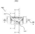
- FIG. 4 is a rear view of the filter circuit device 800 as seen from the direction of the arrow in the direction E shown in FIG. 3.
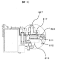
- FIG. 10 is a cross-sectional view of a cross section obtained by cutting the filter circuit device 800 from the arrow direction of the FF cross section shown in FIG. 9. It is sectional drawing of the cross section which cut
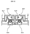
- FIG. 4 is a top view of the filter circuit device 800 as seen from the direction of the arrow in the direction H shown in FIG. 3.
- 13 is a partially enlarged view of a range I shown in FIG. 12 in the filter circuit device 800.
- FIG. It is a front view of the state which assembled the 1st core member 814, the 2nd core member 816, and the direct current
- FIG. 1 is an external perspective view of a power conversion apparatus 100 according to the present embodiment.
- FIG. 2 is an exploded perspective view of the power conversion apparatus 100 according to the present embodiment.
- the power semiconductor module 300 has a plurality of power semiconductor elements, and converts DC power into AC power by switching operation of the power semiconductor elements.
- the capacitor module 230 smoothes the DC power and supplies the smoothed DC power to the power semiconductor module 300.
- the high-voltage DC connector 240 transmits DC power from the battery to the filter circuit device 800 described later.
- the AC current conductor 400 supplies AC power to the motor.
- the drive circuit board 510 calculates a drive signal for driving the power semiconductor element, and further outputs it to the power semiconductor module 300.
- the weak electric signal connector 250 connects the integrated control circuit unit and the control circuit board 500 to transmit and receive a control command signal and the like.
- the control circuit board 500 generates a control signal for controlling the drive circuit board 510 based on the control command signal, and outputs the control signal to the drive circuit board 510.
- the metal base 280 is disposed between the control circuit board 500 and the drive circuit board 510.
- the metal base 280 is connected to the case 200 that is grounded.
- the metal base 280 functions as a shielding plate that shields noise generated from the power semiconductor module 300, the drive circuit board 510, and the like.
- the excitation connector 260 is connected to the housing case 200 and transmits an excitation signal to the excitation circuit module 600.
- the housing case 200 is provided with a screw hole, and the excitation connector 260 is connected to the housing case 200 by a screw, but may be connected by other methods.
- the filter circuit cover 290 is connected to the housing case 200 so as to cover the filter circuit device 800.
- the discharge resistor 700 discharges the electric charge accumulated in the capacitor module 230.
- the housing case 200 accommodates the capacitor module 230 in one space (the lower region of the power conversion device 100 in FIG. 2), and is described above in the other space (the upper region of the power conversion device 100 in FIG. 2). Houses other electrical circuit components.
- the refrigerant inflow pipe 210IN and the refrigerant outflow pipe 210OUT are assembled to the housing case 200 to allow the refrigerant to flow in or out.
- the housing lower cover 220 and the housing upper cover 270 are assembled after each component is stored in the housing case 200.
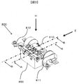
- FIG. 3 is an overall perspective view of the filter circuit device 800 according to the present embodiment.
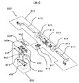
- FIG. 4 is an exploded perspective view of the filter circuit device 800 according to the present embodiment.
- the filter circuit device 800 includes a DC conductor portion 810 and a capacitor circuit portion 850.
- the DC conductor portion 810 forms a first conductor 811, a second conductor 812, a first core member 814 that forms a first through hole 813, and a second through hole 815.
- the first conductor 811 passes through both the first through hole 813 and the second through hole 815.
- the second conductor 812 passes through both the first through hole 813 and the second through hole 815.
- the capacitor circuit unit 850 includes the first common mode capacitor 851, the second common mode capacitor 852, and the two normal noise capacitors 853 to form a noise suppression unit.
- the capacitor case 854 forms a space for storing each capacitor.
- the capacitor case 854 contains a first common mode capacitor 851, a second common mode capacitor 852, and two normal noise capacitors 853, and each capacitor is combined into one.
- a plurality of capacitor cases 854 may be used, and each capacitor may be combined into two or more shapes, or may be combined by a method other than the capacitor case 854.
- the first relay terminal 855 electrically connects the first terminal 817 and each capacitor.
- the second relay terminal 856 electrically connects the second terminal 818 and each capacitor.
- the ground terminal 857 grounds the normal noise capacitor 853.
- the capacitor cover 858 functions as a lid for closing the opening of the capacitor case 854.
- the number of common mode capacitors may be less than two, or Three or more may be used.
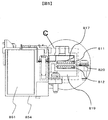
- FIG. 5 is a cross-sectional view of the cross section of the filter circuit device 800 cut from the arrow direction of the AA cross section shown in FIG.
- the first conductor 811 and the second conductor 812 that pass through the first through hole 813 and the second through hole 815 have a facing portion 820 whose main surfaces face each other.
- the main surface of the first conductor 811 and the main surface of the second conductor 812 refer to surfaces having a larger surface area than other surfaces.
- FIG. 6 is an enlarged view of a range C of the cross-sectional view of the filter circuit device 800 shown in FIG.
- the first terminal 817 presses the side surface 822 opposite to the facing surface 821 of the first conductor 811 and is in contact with the first conductor 811.
- a spring plate member is used for the first terminal 817, and the first terminal 817 is inserted into the insertion space 823 of the resin fixing portion 819 and the first conductor 811.
- the first terminal 817 is pressed against the opposite side surface 822 of the first conductor 811 by a reaction force generated when the first terminal 817 is inserted into the insertion space 823.
- the first terminal 817 may be pressed by another means such as pressing the first terminal 817 against the first conductor 811 by another member.
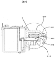
- FIG. 7 is a cross-sectional view of the cross section of the filter circuit device 800 cut from the arrow direction of the BB cross section shown in FIG.
- FIG. 8 is an enlarged view of a range D of the sectional view of the filter circuit device 800 shown in FIG.
- the second terminal 818 is pressed against the side surface 825 opposite to the facing surface 824 of the second conductor 812 and is in contact with the second conductor 812.
- the second terminal 818 is a spring plate member, and the second terminal 818 is inserted into the insertion space 826 between the resin fixing portion 819 and the second conductor 812.
- the second terminal 818 is pressed against the opposite side surface 825 of the second conductor 812 by a reaction force generated when the second terminal 818 is inserted into the insertion space 826.
- the second terminal 818 may be pressed by another means such as pressing the second terminal 818 against the second conductor 812 by another member.
- the core when the conductor penetrates the core of the first core member 814 and the second core portion 816, the core constitutes an inductor.
- the inductor has a high impedance with respect to a component having a high frequency. For this reason, it is difficult for high-frequency noise components to pass through, and it has a performance as a low-pass filter.
- the first conductor 811 and the second conductor 812 are passed through the first core member 814 and the second core member 816. That is, the first core member 814 and the second core member 816 form a double noise filter, thereby improving noise removal performance.
- Power converters are desired to be lighter, smaller, and lower in cost, and noise filters housed in power converters are required to be light, small, and low cost while having high noise removal capability. .
- a small core is used while ensuring noise removal capability, and a conductor that penetrates the core is one that is not assembled with a large fastening component such as a large stud.
- the reason for not installing a large stud or the like is to prevent an increase in weight, space and cost due to an increase in the number of parts.
- the reduction in the number of parts also reduces the number of assembly steps, leading to improved assembly and cost reduction.
- the capacitor has a high impedance with respect to a component having a low frequency. For this reason, it is difficult for noise components having a low frequency to pass therethrough, and it has a performance as a high-pass filter.
- a plurality of capacitors having different capacities are used to improve noise removal performance in an arbitrary low frequency range.
- the first conductor 811 and the second conductor 812 have a facing portion 820 between the first conductor 811 and the second conductor 812, and a side surface opposite to the facing portion 820 (a side surface 822 opposite to the first conductor 811, a second side). Opposite side surface 825 of conductor 812) The first terminal 817 and the second terminal 818 are pressed.
- the noise removal capability is not lowered, and the number of parts is reduced, leading to weight reduction, size reduction, cost reduction, and assembly improvement.
- FIG. 9 is a rear view of the filter circuit device 800 as seen from the direction of the arrow in the direction E shown in FIG.
- FIG. 10 is a cross-sectional view of a cross section of the filter circuit device 800 taken along the arrow direction of the FF cross section shown in FIG.
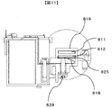
- FIG. 11 is a cross-sectional view of the cross section of the filter circuit device 800 cut from the arrow direction of the GG cross section shown in FIG.
- the first terminal 817 is pressed against the opposite side surface 822 of the first conductor 811 by the first pressing member 827. Further, as shown in FIG. 11, like the first terminal 817, the second terminal 818 is pressed against the opposite side surface 825 of the second conductor 818 by the second pressing member 828.
- the first pressing member 827 and the second pressing member 828 are, for example, screw mechanisms, but may be other members as long as the first terminal 817 and the second conductor 818 can be pressed.
- FIG. 12 is a top view of the filter circuit device 800 as seen from the direction of the arrow H in FIG. FIG. 12 is also a view of the first conductor 811 as viewed from the direction perpendicular to the facing surface 821.
- the first terminal 817 and the second terminal 818 are arranged at positions that do not overlap with each other, and a part of the capacitor circuit unit 850 is sandwiched between the first terminal 817 and the second terminal 818. Be placed.
- One means for reducing the assembly process and improving the assemblability is to unify the screw insertion directions of the first pressing member 827 and the second pressing member 828.
- the filter circuit device 800 is inserted into the housing case of the power converter and screwed in the direction seen from the direction perpendicular to the facing surface 821. Thereby, screw fastening can be performed without changing the direction of the housing case, and assemblability can be improved.
- one way to save space for component placement is to reduce dead space.
- the space for housing the filter circuit device 800 in the housing case is limited, and there is a dimensional restriction on the capacitor to be used, and the capacitor circuit unit 850 needs to be arranged so as not to create a dead space as much as possible. It has become.
- the capacitor circuit unit 850 is inserted between the first terminal 817 and the second terminal 818 while the capacitor circuit unit 850 enters the dead space between the first core member 814 and the second core member 816.
- the dead space can be reduced by arranging them at positions sandwiched between the two.
- FIG. 13 is a partially enlarged view of the range I shown in FIG. 12 in the filter circuit device 800.
- the capacitor circuit unit 850 has a structure in which capacitors are integrated, and the terminal portion of the capacitor to be used is a cylindrical lead wire.
- connection to the capacitor terminal portion by welding or soldering can be mentioned, but a structure that prevents cracks in the welding portion or soldering portion due to external force is required. Therefore, in this embodiment, when assembling the capacitor circuit portion 850, the first capacitor side terminal 859 and the second capacitor side terminal 860 are incorporated to ensure electrical connection by welding or soldering, and external force is applied to the welded portion or solder portion. It is difficult to join.
- the first terminal 817 is formed of a member different from the first capacitor side terminal 859 and the first capacitor side terminal 859 provided on the side close to the first capacitor side, and is in contact with the first conductor 811. 829.
- the second terminal 818 is formed of a second capacitor side terminal 860 provided on the side close to the second capacitor side, and the second capacitor side terminal 860 is formed of a separate member and is in contact with the second conductor 812. Terminal 830.
- FIG. 14 is a front view showing a state in which the first core member 814, the second core member 816, and the DC conductor portion 810 are assembled.
- the resin fixing portion 819 supports the first core member 814, the second core member 816, the first conductor 811, the second conductor 812, the first conductor side terminal 829, and the second conductor side terminal 830.
- the resin fixing portion 819 also has a function of insulating the first conductor 811, the second conductor 812, the first conductor side terminal 829, and the second conductor side terminal 830 through which current flows, and preventing a short circuit.
- SYMBOLS 100 Power converter device 200 ... Housing
Landscapes
- Engineering & Computer Science (AREA)
- Power Engineering (AREA)
- Microelectronics & Electronic Packaging (AREA)
- Physics & Mathematics (AREA)
- Electromagnetism (AREA)
- Manufacturing & Machinery (AREA)
- Inverter Devices (AREA)
- Filters And Equalizers (AREA)
- Coils Or Transformers For Communication (AREA)
- Dc-Dc Converters (AREA)
Abstract
本発明の課題は、ノイズ抑制機能を維持又は向上させながら装置の小型化を図ることである。 本発明に係るフィルタ回路装置は、第1貫通孔を形成する第1コア部材と、第2貫通孔を形成する第2コア部材と、前記第1貫通孔及び前記第2貫通孔を通る第1導体と、前記第1貫通孔及び前記第2貫通孔を通る第2導体と、コンデンサと、前記第1導体と前記コンデンサを電気的に接続する第1端子と、前記第2導体と前記コンデンサを電気的に接続する第2端子と、を備え、前記第1貫通孔から前記第2巻通孔までの前記第1導体及び前記第2導体において、前記第1導体と前記第2導体との対向部を有し、前記第1端子は、前記第1導体の対向面とは反対側面を押圧して接触し、前記第2端子は、前記第2導体の対向面とは反対側面を押圧して接触する。
Description
フィルタ回路装置及びそれを備えた電力変換装置に係り、特に電動車両に用いられるフィルタ回路装置及びそれを備えた電力変換装置に係る。
電気自動車やハイブリッド自動車においては、バッテリの電力により走行用回転電機を駆動するための電力変換装置を搭載している。電気自動車あるいはハイブリッド自動車用の電力変換装置においては、居住スペースの確保などの観点から、装置の小型化に対する要求が強い。
装置の小型化とともに部品が集積化され、部品間に送受する可能性があるノイズの伝播を抑制する必要が生じる。そのために、電力を伝送する導体にコア部材を含むフィルタ装置を備える場合がある(特許文献1)。
しかしながら、自動車の電動化が急速に進む中ではノイズ抑制機能を維持又は向上させながら装置の小型化を図ることが更に求められている。
本発明の課題は、ノイズ抑制機能を維持又は向上させながら装置の小型化を図ることである。
本発明に係るフィルタ回路装置は、第1貫通孔を形成する第1コア部材と、第2貫通孔を形成する第2コア部材と、前記第1貫通孔及び前記第2貫通孔を通る第1導体と、前記第1貫通孔及び前記第2貫通孔を通る第2導体と、コンデンサと、前記第1導体と前記コンデンサを電気的に接続する第1端子と、前記第2導体と前記コンデンサを電気的に接続する第2端子と、を備え、前記第1貫通孔から前記第2巻通孔までの前記第1導体及び前記第2導体において、前記第1導体と前記第2導体との対向部を有し、前記第1端子は、前記第1導体の対向面とは反対側面を押圧して接触し、前記第2端子は、前記第2導体の対向面とは反対側面を押圧して接触する。
本発明により、ノイズ抑制機能を維持又は向上させながら装置の小型化を図ることができる。
以下、図面を参照して、本発明に係る電力変換装置の実施の形態について説明する。なお、各図において同一要素については同一の符号を記し、重複する説明は省略する。本発明は以下の実施形態に限定されることなく、本発明の技術的な概念の中で種々の変形例や応用例をもその範囲に含むものである。
図1は、本実施形態に係る電力変換装置100の外観斜視図である。図2は、本実施形態に係る電力変換装置100の分解斜視図である。
パワー半導体モジュール300は、パワー半導体素子を複数有し、パワー半導体素子のスイッチング動作により直流電力を交流電力に変換する。コンデンサモジュール230は、直流電力を平滑化し、平滑化された直流電力をパワー半導体モジュール300に供給する。
強電直流用コネクタ240は、バッテリからの直流電力を後述するフィルタ回路装置800に伝達する。交流電流用導体部400は、モータに交流電力を供給する。
駆動回路基板510は、パワー半導体素子を駆動するための駆動信号を演算し、さらにパワー半導体モジュール300に出力する。弱電信号用コネクタ250は、統合制御回路部等と制御回路基板500を繋ぎ、制御指令信号等を送受信する。制御回路基板500は、制御指令信号に基づき駆動回路基板510を制御するための制御信号を生成し、さらに駆動回路基板510に出力する。
金属ベース280は、制御回路基板500と駆動回路基板510の間に配置される。金属ベース280は、グランドに接地された筐体ケース200に接続される。金属ベース280は、パワー半導体モジュール300や駆動回路基板510等から発生するノイズを遮蔽する遮蔽板と機能する。
励磁用コネクタ260は、筐体ケース200に接続され、励磁回路モジュール600に励磁信号を伝達する。
本実施形態では、筐体ケース200にネジ穴を設け、励磁用コネクタ260をネジによって筐体ケース200に接続されるが、その他の方法で接続されても良い。
フィルタ回路カバー290は、フィルタ回路装置800を覆うように、筐体ケース200に接続される。放電抵抗700は、コンデンサモジュール230に溜まった電荷を放電する。
筐体ケース200は、一方側の空間(図2では電力変換装置100の下部領域)にコンデンサモジュール230を収納し、他方側の空間に(図2では電力変換装置100の上部領域)に上述した他の電気回路部品を収納する。
冷媒流入用パイプ210IN及び冷媒流出用パイプ210OUTは、筐体ケース200に組み付けられ、冷媒を流入または流出させる。
筐体下部カバー220及び筐体上部カバー270は、筐体ケース200に各部品を収納した後に組み付けられる。
図3は、本実施形態に係るフィルタ回路装置800の全体斜視図である。図4は、本実施形態に係るフィルタ回路装置800の分解斜視図である。
フィルタ回路装置800は、直流用導体部810と、コンデンサ回路部850と、から構成されている。
図4に示されるように、直流用導体部810は、第1導体811と、第2導体812と、第1貫通孔813を形成する第1コア部材814と、第2貫通孔815を形成する第2コア部材816と、第1導体811とコンデンサ回路部850を電気的に接続するための第1端子817と、第2導体812とコンデンサ回路部850を電気的に接続するための第2端子818と、樹脂製固定部819と、によって構成される。
第1導体811は、第1貫通孔813及び第2貫通孔815の双方を通る。第2導体812は、第1貫通孔813及び第2貫通孔815の双方を通る。
コンデンサ回路部850は、第1コモンモード用コンデンサ851と、第2コモンモード用コンデンサ852と、2つのノーマルノイズ用コンデンサ853と、によりノイズ抑制部を構成する。またコンデンサ用ケース854は、各コンデンサを収納する空間を形成する。
本実施形態では、コンデンサ用ケース854へ第1コモンモード用コンデンサ851と、第2コモンモード用コンデンサ852と、2つのノーマルノイズ用コンデンサ853を収納し、各コンデンサを1つにまとめた形状をしているが、コンデンサ用ケース854を複数使用し各コンデンサを2つ以上にまとめた形状にしても良い、またはコンデンサ用ケース854以外の方法でまとめても良い。
第1中継端子855は、第1端子817と各コンデンサとの間を電気的に接続する。第2中継端子856は、第2端子818と各コンデンサとの間を電気的に接続する。接地用端子857は、ノーマルノイズ用コンデンサ853を接地する。
コンデンサ用カバー858は、コンデンサ用ケース854の開口部に塞ぐための蓋として機能する。
本実施形態では静電容量が違う第1コモンモード用コンデンサ852と第2コモンモード用コンデンサ853の2つが配置されているが、コモンモード用コンデンサの数を2つ未満にしていても良く、または3つ以上にしても良い。
図5は、図3に示すA―A断面の矢印方向からフィルタ回路装置800を切断した断面の断面図である。
図5に示すように、第1貫通孔813及び第2貫通孔815を通る第1導体811及び第2導体812は、それぞれの主面が対向する対向部820を有している。ここで、第1導体811の主面及び第2導体812の主面とは、他の面に比して表面積が大きい面を指す。
図6は、図5に示されたフィルタ回路装置800の断面図の範囲Cの拡大図である。
第1端子817は、第1導体811の対向面821とは反対側面822を押圧し、第1導体811に接触している。
本実施形態では、第1端子817は、ばね板状部材が用いられ、樹脂製固定部819と第1導体811の差し込み空間823に第1端子817を差し込まれる。第1端子817が差し込み空間823に差し込まれる際に生じる反力によって、第1端子817を第1導体811の反対側面822に押圧している。第1端子817を別部材によって第1導体811へ押圧するといった、別手段によって押圧されていても良い。
図7は、図3に示すB―B断面の矢印方向からフィルタ回路装置800を切断した断面の断面図である。図8は、図7に示されたフィルタ回路装置800の断面図の範囲Dの拡大図である。
第2端子818は、第2導体812の対向面824とは反対側面825に押圧し、第2導体812に接触している。
本実施形態では、第2端子818は、ばね板状部材を用いられ、樹脂製固定部819と第2導体812の差し込み空間826に第2端子818を差し込まれる。第2端子818が差し込み空間826に差し込まれる際に生じる反力によって、第2端子818を第2導体812の反対側面825に押圧している。第2端子818を別部材によって第2導体812へ押圧するといった、別手段によって押圧されていても良い。
ここで、本実施形態に係る発明の原理を説明する。第1導体811や第2導体812等の導体に電気が流れた場合、導体の周辺には磁界が発生し、発生した磁界によってノイズが発生する。
一方、導体が第1コア部材814と第2コア部816のコアを貫通すると、コアがインダクタを構成する。インダクタは、周波数の高い成分に対してインピーダンスが高くなる。そのため周波数の高いノイズ成分は通りにくくなり、ローパスフィルタとしての性能を持つ。
本実施形態では、第1コア部材814と第2コア部材816に、第1導体811と第2導体812を貫通させている。つまり第1コア部材814と第2コア部材816が二重にノイズフィルタを形成させることにより、ノイズ除去の性能を向上させている。
電力変換装置は、軽量化や小型化や低コスト化が望まれ、電力変換装置内に収納されるノイズフィルタは、高いノイズ除去能力を有しつつ、軽量小型かつ低コストであることが求められる。
本実施形態では、ノイズ除去能力を確保しながら小型なコアを使用し、またコアに貫通する導体は大きなスタッド等の大きな締結部品を組み付けてないものを使用する。大きなスタッド等を組付けない理由は、部品点数増加による重量の増加、スペース及びコストの増加を防ぐためである。また部品点数が削減できることにより、組立工程数の削減にもなり、組立性向上とコスト低減につながる。
またコアを使用する以外に、他のノイズを除去する手段として、コンデンサがある。コンデンサは、周波数が低い成分に対してインピーダンスが高くなる。そのため周波数が低いノイズ成分は通りにくくなり、ハイパスフィルタとしての性能を持つ。本実施形態では、容量の異なるコンデンサを複数使用し、任意の低周波域のノイズ除去の性能を向上させている。
導体同士を接続する手段として、押圧がある。第1導体811及び第2導体812は、第1導体811と第2導体812との対向部820を有しており、対向部820とは反対側面(第1導体811の反対側面822、第2導体812の反対側面825)第1端子817及び第2端子818を押圧させている。
本実施形態により、非分割タイプのコアを使用できる構造にしても、ノイズ除去能力を低下せず、部品点数削減により、軽量化、小型化、低コスト化、組立性向上につながる。
図9は、図3に示す方向Eの矢印方向から見た、フィルタ回路装置800の背面図である。図10は、図9に示すF―F断面の矢印方向からフィルタ回路装置800を切断した断面の断面図である。図11は、図9に示すG―G断面の矢印方向からフィルタ回路装置800を切断した断面の断面図である。
図10に示されるように、第1端子817は、第1押圧部材827によって第1導体811の反対側面822に押圧される。また図11に示されるように、第1端子817と同様に、第2端子818は、第2押圧部材828によって第2導体818の反対側面825に押圧される。
第1押圧部材827及び第2押圧部材828は、例えばネジ機構であるが、第1端子817及び第2導体818を押圧することができれば他の部材であってもよい。
図12は、図3に示す方向Hの矢印方向から見た、フィルタ回路装置800の上面図である。また図12は、第1導体811の対向面821の直角方向から見た図でもある。
図12に示すように、第1端子817と第2端子818は、互いに重ならない位置に配置され、コンデンサ回路部850の一部が第1端子817と第2端子818の間に挟まれる位置に配置される。
組立時の工程を削減し組立性を向上させる1つの手段として、第1押圧部材827や第2押圧部材828のネジの挿入向きの統一が挙げられる。
本実施形態では、対向面821の直角方向から見た向きでフィルタ回路装置800を電力変換装置の筐体ケース挿入しネジ締結する構造となっている。これにより、筐体ケースの向きを変更することなくネジ締結を行うことができ、組立性を向上させることができる。
また部品配置の省スペース化の1つの手段として、デッドスペースの削減が挙げられる。本実施形態では、筐体ケースにフィルタ回路装置800を収納するスペースが限られており、また使用するコンデンサにも寸法制約あり、コンデンサ回路部850は可能な限りデッドスペースを作らない配置が必要となっている。
図12に示すように、第1コア部材814と第2コア部材816の間にあるデッドスペースへコンデンサ回路部850を侵入させつつ、コンデンサ回路部850を第1端子817と第2端子818の間に挟まれる位置に配置させることにより、デッドスペースを削減することができる。
図13は、フィルタ回路装置800において図12に示される範囲Iの部分拡大図である。
実施形態では、コンデンサ回路部850にコンデンサをまとめた構造となっており、また使用するコンデンサの端子部は円柱状のリード線となっている。容易にコンデンサと電気的接続をするには、コンデンサ端子部と溶接または半田による接続が挙げられるが、外力が加わることによる溶接部またははんだ部のクラックを防ぐ構造が必要となる。そこで本実施形態では、コンデンサ回路部850を組立てる際に、第1コンデンサ側端子859及び第2コンデンサ側端子860を組み込み、溶接あるいははんだによって電気的接続を確保し、溶接部あるいははんだ部に外力が加わりにくい構造となっている。
第1端子817は、第1コンデンサ側に近い側に設けられる第1コンデンサ側端子859と、第1コンデンサ側端子859とは別部材で形成されかつ第1導体811に接触する第1導体側端子829と、により構成される。
また第2端子818は、第2コンデンサ側に近い側に設けられる第2コンデンサ側端子860と、第2コンデンサ側端子860とは別部材で形成されかつ第2導体812に接触する第2導体側端子830と、により構成される。
図14は、第1コア部材814と第2コア部材816と直流用導体部810を組んだ状態の正面図である。
樹脂製固定部819は、第1コア部材814と第2コア部材816と第1導体811と第2導体812と第1導体側端子829と第2導体側端子830を支持する。
これにより各部品を1つのサブアッセンブリ部品としてまとめることにより組立性向上を図ることができる。また樹脂製固定部819は、電流が流れる第1導体811と第2導体812と第1導体側端子829と第2導体側端子830をそれぞれ絶縁し、かつ短絡を防ぐ働きも備えている。
100…電力変換装置、200…筐体ケース、210IN…冷媒流入用パイプ、210OUT…冷媒流出用パイプ、230…コンデンサモジュール、240…強電直流用コネクタ、250…弱電信号用コネクタ、260…励磁用コネクタ、280…金属ベース、290…フィルタ回路カバー、300…パワー半導体モジュール、400…交流電流用導体部、500…制御回路基板、510…駆動回路基板、700…放電抵抗、800…フィルタ回路装置、810…直流用導体部、811…第1導体、812…第2導体、813…第1貫通孔、814…第1コア部材、815…第2貫通孔、816…第2コア部材、817…第1端子、818…第2端子、819…樹脂製固定部、820…対向部、821…対向面、822…反対側面、823…差し込み空間、825…反対側面、826…差し込み空間、827…第1押圧部材、828…第2押圧部材、829…第1導体側端子、830…第2導体側端子、850…コンデンサ回路部、851…第1コモンモード用コンデンサ、852…第2コモンモード用コンデンサ、853…ノーマルノイズ用コンデンサ、854…コンデンサ用ケース、855…第1中継端子、856…第2中継端子、857…接地用端子、858…コンデンサ用カバー、859…第1コンデンサ側端子、860…第2コンデンサ側端子
Claims (7)
- 第1貫通孔を形成する第1コア部材と、
第2貫通孔を形成する第2コア部材と、
前記第1貫通孔及び前記第2貫通孔を通る第1導体と、
前記第1貫通孔及び前記第2貫通孔を通る第2導体と、
コンデンサと、
前記第1導体と前記コンデンサを電気的に接続する第1端子と、
前記第2導体と前記コンデンサを電気的に接続する第2端子と、を備え、
前記第1貫通孔から前記第2巻通孔までの前記第1導体及び前記第2導体において、前記第1導体と前記第2導体との対向部を有し、
前記第1端子は、前記第1導体の対向面とは反対側面を押圧して接触し、
前記第2端子は、前記第2導体の対向面とは反対側面を押圧して接触するフィルタ回路装置。 - 請求項1に記載されたフィルタ回路装置であって、
前記第1端子を前記第1導体に押圧する第1押圧部材と、
前記第2端子を前記第2導体に押圧する第2押圧部材と、を備えるフィルタ回路装置。 - 請求項1または2に記載されたフィルタ回路装置であって、
前記第1導体の対向面の直角方向から見た場合、
前記第1端子と前記第2端子は、互いに重ならない位置に配置され、
前記コンデンサは、前記第1端子と前記第2端子の間に挟まれる位置に配置されるフィルタ回路装置。 - 請求項1ないし3に記載されたいずれかのフィルタ回路装置であって、
前記第1端子は、前記コンデンサ側に近い側に設けられる第1コンデンサ側端子と、当該第1コンデンサ側端子とは別部材で形成されかつ前記第1導体に接触する第1導体側端子と、により構成され、
前記第2端子は、前記コンデンサ側に近い側に設けられる第2コンデンサ側端子と、当該第2コンデンサ側端子とは別部材で形成されかつ前記第2導体に接触する第2導体側端子と、により構成されるフィルタ回路装置。 - 請求項4に記載されたフィルタ回路装置であって、
前記第1コア部材と前記第2コア部材と前記第1導体と前記第2導体と前記第1導体側端子と前記第2導体側端子を支持する樹脂製固定部を備えるフィルタ回路装置。 - 請求項1ないし5に記載されたいずれかのフィルタ回路装置を備えた電力変換装置であって、
直流電力を交流電力に変換するパワー半導体モジュールと、
前記直流電力を平滑化するコンデンサモジュールと、を備え、
前記フィルタ回路装置は、前記コンデンサモジュールに供給される直流電力のノイズを除去する電力変換装置。 - 請求項6に記載された電力変換装置であって、
前記パワー半導体モジュールと前記フィルタ回路装置を収納する空間を形成する筐体と、
前記前記パワー半導体モジュールと前記フィルタ回路装置の間の空間に配置されかつ前記筐体に接続されるカバーと、を備える電力変換装置。
Priority Applications (4)
| Application Number | Priority Date | Filing Date | Title |
|---|---|---|---|
| CN201880087429.5A CN111630761B (zh) | 2018-02-02 | 2018-12-26 | 滤波电路装置及具备该滤波电路装置的电力转换装置 |
| JP2019568945A JP6942822B2 (ja) | 2018-02-02 | 2018-12-26 | フィルタ回路装置及びそれを備えた電力変換装置 |
| US16/965,981 US11798749B2 (en) | 2018-02-02 | 2018-12-26 | Power converter including filter circuit device to improve a noise suppression function |
| DE112018006748.3T DE112018006748B4 (de) | 2018-02-02 | 2018-12-26 | Filterschaltungsvorrichtung und stromrichter umfassend filterschaltungsvorrichtung |
Applications Claiming Priority (2)
| Application Number | Priority Date | Filing Date | Title |
|---|---|---|---|
| JP2018016876 | 2018-02-02 | ||
| JP2018-016876 | 2018-02-02 |
Publications (1)
| Publication Number | Publication Date |
|---|---|
| WO2019150859A1 true WO2019150859A1 (ja) | 2019-08-08 |
Family
ID=67478027
Family Applications (1)
| Application Number | Title | Priority Date | Filing Date |
|---|---|---|---|
| PCT/JP2018/047724 Ceased WO2019150859A1 (ja) | 2018-02-02 | 2018-12-26 | フィルタ回路装置及びそれを備えた電力変換装置 |
Country Status (5)
| Country | Link |
|---|---|
| US (1) | US11798749B2 (ja) |
| JP (1) | JP6942822B2 (ja) |
| CN (1) | CN111630761B (ja) |
| DE (1) | DE112018006748B4 (ja) |
| WO (1) | WO2019150859A1 (ja) |
Cited By (3)
| Publication number | Priority date | Publication date | Assignee | Title |
|---|---|---|---|---|
| CN114731110A (zh) * | 2020-03-31 | 2022-07-08 | Tdk电子股份有限公司 | 具有改进衰减的dc-链路的emc滤波器部件、半导体部件和dc-链路emc系统 |
| WO2023002623A1 (ja) * | 2021-07-21 | 2023-01-26 | 日立Astemo株式会社 | 電力変換装置、電力変換装置の製造方法 |
| CN115699550A (zh) * | 2020-06-08 | 2023-02-03 | 三菱电机株式会社 | 噪声滤波器及使用该噪声滤波器的电力转换装置 |
Families Citing this family (1)
| Publication number | Priority date | Publication date | Assignee | Title |
|---|---|---|---|---|
| CN115580155A (zh) * | 2021-06-21 | 2023-01-06 | 上海汽车电驱动有限公司 | 一种新能源汽车用过滤整流装置 |
Citations (5)
| Publication number | Priority date | Publication date | Assignee | Title |
|---|---|---|---|---|
| JP2015201957A (ja) * | 2014-04-08 | 2015-11-12 | 株式会社ジェイテクト | モータ制御装置 |
| JP2016024939A (ja) * | 2014-07-18 | 2016-02-08 | 北川工業株式会社 | フィルター付き端子台 |
| JP2016514387A (ja) * | 2013-02-11 | 2016-05-19 | エプコス アクチエンゲゼルシャフトEpcos Ag | フィルタデバイス |
| JP2017098384A (ja) * | 2015-11-20 | 2017-06-01 | 株式会社安川電機 | 電力変換装置及びノイズフィルタ |
| JP2017208943A (ja) * | 2016-05-19 | 2017-11-24 | 日立オートモティブシステムズ株式会社 | 電力変換装置 |
Family Cites Families (14)
| Publication number | Priority date | Publication date | Assignee | Title |
|---|---|---|---|---|
| JP2005012106A (ja) * | 2003-06-20 | 2005-01-13 | Ngk Spark Plug Co Ltd | コンデンサ |
| US7973628B1 (en) * | 2004-06-17 | 2011-07-05 | Ctm Magnetics, Inc. | Methods and apparatus for electrical components |
| DE102007059640B4 (de) | 2007-12-10 | 2009-11-26 | Wago Verwaltungsgesellschaft Mbh | Anschlussmodul |
| JP2013219919A (ja) * | 2012-04-09 | 2013-10-24 | Mitsubishi Electric Corp | ノイズ低減フィルタおよびそれを用いた電力変換装置 |
| JP5738817B2 (ja) * | 2012-09-14 | 2015-06-24 | 日立オートモティブシステムズ株式会社 | 電力変換装置 |
| JP5789576B2 (ja) * | 2012-09-14 | 2015-10-07 | 日立オートモティブシステムズ株式会社 | 電力変換装置 |
| JP6072492B2 (ja) * | 2012-10-09 | 2017-02-01 | 日立オートモティブシステムズ株式会社 | コンデンサモジュール及び電力変換装置 |
| JP6152722B2 (ja) * | 2013-07-08 | 2017-06-28 | 株式会社オートネットワーク技術研究所 | ノイズフィルタ装置 |
| US9893603B2 (en) * | 2014-06-06 | 2018-02-13 | Hitachi Automotive Systems, Ltd. | Power converter |
| TWI640019B (zh) * | 2016-12-22 | 2018-11-01 | 善元科技股份有限公司 | 共模電感裝置、共模電感裝置的繞線方法以及電磁干擾濾波電路 |
| DE102017105839A1 (de) * | 2017-03-17 | 2018-09-20 | Schaffner Emv Ag | Aktives Filter |
| JP7127317B2 (ja) * | 2018-03-22 | 2022-08-30 | 日立金属株式会社 | コモンモードチョーク |
| DE112019002805B4 (de) * | 2018-07-04 | 2026-01-08 | Hitachi Astemo, Ltd. | Leistungsumwandlungsvorrichtung |
| US20230071172A1 (en) * | 2020-06-08 | 2023-03-09 | Mitsubishi Electric Corporation | Noise filter and power conversion device using same |
-
2018
- 2018-12-26 CN CN201880087429.5A patent/CN111630761B/zh active Active
- 2018-12-26 US US16/965,981 patent/US11798749B2/en active Active
- 2018-12-26 WO PCT/JP2018/047724 patent/WO2019150859A1/ja not_active Ceased
- 2018-12-26 DE DE112018006748.3T patent/DE112018006748B4/de active Active
- 2018-12-26 JP JP2019568945A patent/JP6942822B2/ja active Active
Patent Citations (5)
| Publication number | Priority date | Publication date | Assignee | Title |
|---|---|---|---|---|
| JP2016514387A (ja) * | 2013-02-11 | 2016-05-19 | エプコス アクチエンゲゼルシャフトEpcos Ag | フィルタデバイス |
| JP2015201957A (ja) * | 2014-04-08 | 2015-11-12 | 株式会社ジェイテクト | モータ制御装置 |
| JP2016024939A (ja) * | 2014-07-18 | 2016-02-08 | 北川工業株式会社 | フィルター付き端子台 |
| JP2017098384A (ja) * | 2015-11-20 | 2017-06-01 | 株式会社安川電機 | 電力変換装置及びノイズフィルタ |
| JP2017208943A (ja) * | 2016-05-19 | 2017-11-24 | 日立オートモティブシステムズ株式会社 | 電力変換装置 |
Cited By (7)
| Publication number | Priority date | Publication date | Assignee | Title |
|---|---|---|---|---|
| CN114731110A (zh) * | 2020-03-31 | 2022-07-08 | Tdk电子股份有限公司 | 具有改进衰减的dc-链路的emc滤波器部件、半导体部件和dc-链路emc系统 |
| CN115699550A (zh) * | 2020-06-08 | 2023-02-03 | 三菱电机株式会社 | 噪声滤波器及使用该噪声滤波器的电力转换装置 |
| EP4164109A4 (en) * | 2020-06-08 | 2023-08-02 | Mitsubishi Electric Corporation | NOISE FILTER AND CURRENT CONVERSION DEVICE USING SAID NOISE FILTER |
| CN115699550B (zh) * | 2020-06-08 | 2025-12-02 | 三菱电机株式会社 | 噪声滤波器及使用该噪声滤波器的电力转换装置 |
| WO2023002623A1 (ja) * | 2021-07-21 | 2023-01-26 | 日立Astemo株式会社 | 電力変換装置、電力変換装置の製造方法 |
| JPWO2023002623A1 (ja) * | 2021-07-21 | 2023-01-26 | ||
| JP7551931B2 (ja) | 2021-07-21 | 2024-09-17 | 日立Astemo株式会社 | 電力変換装置、電力変換装置の製造方法 |
Also Published As
| Publication number | Publication date |
|---|---|
| CN111630761B (zh) | 2023-09-22 |
| JP6942822B2 (ja) | 2021-09-29 |
| JPWO2019150859A1 (ja) | 2021-01-07 |
| CN111630761A (zh) | 2020-09-04 |
| US20210036675A1 (en) | 2021-02-04 |
| DE112018006748T5 (de) | 2020-09-24 |
| US11798749B2 (en) | 2023-10-24 |
| DE112018006748B4 (de) | 2025-01-23 |
Similar Documents
| Publication | Publication Date | Title |
|---|---|---|
| US11025141B2 (en) | On-board electric compressor with a motor and noise reducing unit with inverter device having a damping unit reducing Q value of low pass filter circuit | |
| JP6897671B2 (ja) | 車載用の電力変換装置 | |
| KR102036203B1 (ko) | 노이즈 신호를 억제하기 위한 emc-필터 | |
| US11097592B2 (en) | On-board electric compressor | |
| US9447924B2 (en) | Motor driven compressor for a vehicle | |
| JP6942822B2 (ja) | フィルタ回路装置及びそれを備えた電力変換装置 | |
| KR101851081B1 (ko) | 출력 노이즈 저감 장치 | |
| JP2010187436A (ja) | インバータ装置およびインバータ一体型電動圧縮機 | |
| CN110318976B (zh) | 车载用电动压缩机 | |
| EP4164109B1 (en) | Noise filter and power conversion device using same | |
| EP3151401B1 (en) | Noise reduction device | |
| CN111106455B (zh) | 组装电气装置的方法、电气装置及包括该电气装置的机动车辆 | |
| JP7454952B2 (ja) | ノイズフィルタおよび電力変換装置 | |
| CN113261192B (zh) | 车载用功率转换装置 | |
| JP2021132427A (ja) | 車載用電動圧縮機 | |
| JP2019103285A (ja) | 電力変換装置 | |
| JP2022016892A (ja) | 電力変換装置 |
Legal Events
| Date | Code | Title | Description |
|---|---|---|---|
| 121 | Ep: the epo has been informed by wipo that ep was designated in this application |
Ref document number: 18903702 Country of ref document: EP Kind code of ref document: A1 |
|
| ENP | Entry into the national phase |
Ref document number: 2019568945 Country of ref document: JP Kind code of ref document: A |
|
| 122 | Ep: pct application non-entry in european phase |
Ref document number: 18903702 Country of ref document: EP Kind code of ref document: A1 |