WO2019150563A1 - タッチパネルセンサー基材の製造方法及びタッチパネルセンサー基材セット - Google Patents
タッチパネルセンサー基材の製造方法及びタッチパネルセンサー基材セット Download PDFInfo
- Publication number
- WO2019150563A1 WO2019150563A1 PCT/JP2018/003687 JP2018003687W WO2019150563A1 WO 2019150563 A1 WO2019150563 A1 WO 2019150563A1 JP 2018003687 W JP2018003687 W JP 2018003687W WO 2019150563 A1 WO2019150563 A1 WO 2019150563A1
- Authority
- WO
- WIPO (PCT)
- Prior art keywords
- sensor
- wiring
- substrate
- base material
- touch panel
- Prior art date
- Legal status (The legal status is an assumption and is not a legal conclusion. Google has not performed a legal analysis and makes no representation as to the accuracy of the status listed.)
- Ceased
Links
Images







Classifications
-
- G—PHYSICS
- G06—COMPUTING OR CALCULATING; COUNTING
- G06F—ELECTRIC DIGITAL DATA PROCESSING
- G06F3/00—Input arrangements for transferring data to be processed into a form capable of being handled by the computer; Output arrangements for transferring data from processing unit to output unit, e.g. interface arrangements
- G06F3/01—Input arrangements or combined input and output arrangements for interaction between user and computer
- G06F3/03—Arrangements for converting the position or the displacement of a member into a coded form
- G06F3/041—Digitisers, e.g. for touch screens or touch pads, characterised by the transducing means
-
- G—PHYSICS
- G06—COMPUTING OR CALCULATING; COUNTING
- G06F—ELECTRIC DIGITAL DATA PROCESSING
- G06F3/00—Input arrangements for transferring data to be processed into a form capable of being handled by the computer; Output arrangements for transferring data from processing unit to output unit, e.g. interface arrangements
- G06F3/01—Input arrangements or combined input and output arrangements for interaction between user and computer
- G06F3/03—Arrangements for converting the position or the displacement of a member into a coded form
- G06F3/041—Digitisers, e.g. for touch screens or touch pads, characterised by the transducing means
- G06F3/044—Digitisers, e.g. for touch screens or touch pads, characterised by the transducing means by capacitive means
Definitions
- the present invention relates to a method for manufacturing a touch panel sensor base material and a touch panel sensor base material set. More specifically, even when manufacturing a touch panel sensor base material having a large area, the quality of the touch panel sensor base material can be improved and the yield can be increased. It is related with the manufacturing method of the touchscreen sensor base material which can also improve, and a touchscreen sensor base material set.
- the touch panel sensor is mounted on, for example, a portable terminal and is used to detect a position touched by a user.
- Patent Documents 1 and 2 propose a technique for increasing the area of an image to be displayed with respect to an image display device.
- the touch panel sensor is often mounted on a relatively small device such as a portable terminal, a technique for increasing the area has not been sufficiently established.
- Such a conventional technique has found room for further improvement in terms of improving quality and improving yield, particularly when manufacturing a touch panel sensor substrate having a large area.
- the subject of this invention is the manufacturing method and touch panel sensor base material set of the touch panel sensor base material which can improve the quality of a touch panel sensor base material especially also when manufacturing a large area touch panel sensor base material, and can also improve a yield. Is to provide.
- a sensor substrate precursor in which a plurality of sensor channels and a plating bus line electrically connected to the plurality of sensor channels are formed;
- the manufacturing method of the touch panel sensor base material according to the above 4 wherein the sensor base material is manufactured by cutting out a region where the plating bus line is provided in the sensor base material precursor. 6).
- a base material set for configuring a touch panel sensor At least one sensor substrate having a sensor pattern portion comprising a plurality of sensor channels;
- the sensor channel of the sensor substrate is constituted by a plurality of conductive thin wires, 16.
- a touch panel sensor base material manufacturing method and a touch panel sensor base material set that can improve the quality of the touch panel sensor base material and also improve the yield, especially when manufacturing a large area touch panel sensor base material. Can be provided.
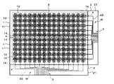
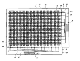
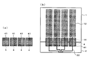
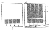
- the figure explaining the example of composition of a sensor channel Diagram explaining connection between sensor substrate and wiring substrate Diagram explaining the method of plating the sensor channel The figure explaining an example of a sensor base material precursor The figure explaining an example of a plating apparatus The figure explaining other examples of a sensor substrate precursor The figure explaining other examples of a sensor substrate precursor The figure explaining other examples of a sensor substrate precursor The figure explaining other examples of a sensor substrate precursor The figure explaining an example of a wiring base material precursor
- a touch panel sensor substrate of the present invention In the method for manufacturing a touch panel sensor substrate of the present invention, at least one sensor substrate having a sensor pattern portion composed of a plurality of sensor channels, and at least one wiring substrate having a lead-out wiring pattern portion composed of a plurality of wires. Then, the sensor substrate and the wiring substrate are connected so that the sensor channel of the sensor substrate and the wiring of the wiring substrate are electrically connected. Thereby, especially when manufacturing a touch panel sensor base material of a large area, the effect which can improve the quality of a touch panel sensor base material and a yield can be acquired.
- FIG. 1 A touch panel sensor manufacturing method according to a first embodiment will be described with reference to FIGS.
- a sensor base material 1 and a wiring base material 2 are prepared.
- the sensor substrate 1 includes a substrate 11 and a plurality of sensor channels 12 provided on the substrate 11.
- a sensor pattern portion S is constituted by the plurality of sensor channels 12.
- the sensor pattern portion S forms an effective area for sensing in the touch panel sensor.
- the base material 11 may be any material that can hold the plurality of sensor channels 12 on the surface in a state of being insulated from each other. Examples thereof include a resin base material (also referred to as a film), a glass base material, and a ceramic base material.
- the material of the film is not particularly limited.
- polyethylene terephthalate (PET) resin polyethylene naphthalate (PEN) resin, polybutylene terephthalate resin, cellulose resin (polyacetyl cellulose, cellulose diacetate, cellulose triacetate, etc.), polyethylene resin Polypropylene resin, methacrylic resin, cyclic polyolefin resin, polystyrene resin, acrylonitrile- (poly) styrene copolymer (AS resin), acrylonitrile-butadiene-styrene copolymer (ABS resin), polyvinyl chloride resin , Poly (meth) acrylic resin, polycarbonate resin, polyester resin, polyimide resin, polyamide resin, polyamideimide resin, cycloolefin polymer (COP) resin And the like. If these materials are used, good insulation and transparency can be imparted to the film. In particular, by using a synthetic resin material, good flexibility can be imparted to the
- the thickness of the substrate 11 is not particularly limited, and can be, for example, about 1 ⁇ m to 10 cm, and further about 20 ⁇ m to 300 ⁇ m.
- the substrate 11 may be subjected to a surface treatment that changes the surface energy.
- the base material 11 may be a laminate, and may have a hard coat layer, an antireflection layer, or the like.
- the base material 11 is rectangular, but the shape of the base material 11 is not limited to this, and an arbitrary shape can be given.
- the sensor channel 12 is an electrode for detecting a touch in the touch panel sensor.
- the detection method of the touch panel sensor is not particularly limited, and examples thereof include a resistance film method, a capacitance method, and an optical sensor method.
- a plurality of sensor channels 12 are arranged at an equal pitch.
- the sensor channel 12 is formed in a strip shape having a predetermined width (also referred to as channel width) with a conductive material.
- the length and width of the sensor channel 12 are not particularly limited, and can be set as appropriate according to the purpose and application.
- the conductive material constituting the sensor channel 12 is not particularly limited, and examples thereof include metal fine particles, metal oxide fine particles, carbon fine particles, and conductive polymers.
- the metal constituting the metal fine particle include Au, Pt, Ag, Cu, Ni, Cr, Rh, Pd, Zn, Co, Mo, Ru, W, Os, Ir, Fe, Mn, Ge, Sn, Ga, In etc. are mentioned. Among these, Au, Ag, and Cu are preferable, and Ag is particularly preferable.
- the average particle diameter of the metal fine particles can be, for example, 1 to 100 nm, further 3 to 50 nm.
- the average particle diameter is a volume average particle diameter, and can be measured by “Zeta Sizer 1000HS” manufactured by Malvern.
- Examples of the metal oxide fine particles include indium tin oxide (ITO) and tin oxide.
- Examples of the carbon fine particles include graphite fine particles, carbon nanotubes, fullerenes and the like. Although it does not specifically limit as a conductive polymer, (pi) conjugated system conductive polymer can be mentioned preferably.
- Examples of the ⁇ -conjugated conductive polymer include polythiophenes and polyanilines. The ⁇ -conjugated conductive polymer may be used together with a polyanion such as polystyrene sulfonic acid.
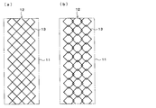
- the sensor channel 12 may be made of a conductive material applied in a solid shape on the base material 11, but in this embodiment, the sensor channel 12 is formed on the base material 11 as shown in FIG. It is constituted by a plurality of conductive thin wires 13 arranged two-dimensionally.
- the sensor channel 12 shown in FIG. 2A is configured by a mesh pattern composed of a plurality of conductive thin wires 13.
- the pattern of the sensor channel 12 may be, for example, a stripe pattern, a random pattern, or the like.
- the pattern of the sensor channel may be a pattern configured by combining a plurality of conductive thin wires forming a geometric figure.
- FIG. 2 (b) shows an example of a sensor channel having a pattern formed by combining a plurality of conductive thin lines forming a geometric figure.
- the sensor channel 12 is composed of a plurality of thin conductive wires 13 that form a quadrangle.
- the pattern of the sensor channel 12 is configured by two-dimensionally arranging a plurality of conductive thin wires 13 forming a quadrangle in the direction of two diagonal lines of the quadrangle.
- the line width of the conductive thin wire 13 constituting the sensor channel 12 is not particularly limited, but may be, for example, 50 ⁇ m or less, 20 ⁇ m or less, preferably 10 ⁇ m or less, 7 ⁇ m or less, and further 5 ⁇ m or less.
- the line width of the conductive thin wire 13 10 ⁇ m or less it is possible to obtain an effect that the sensor channel 12 composed of the conductive thin wire 13 and a pattern (here, a mesh pattern) constituted by the conductive thin wire 13 is less visible.
- the lower limit of the line width of the conductive thin wire 13 is not particularly limited, but can be set to, for example, 1 ⁇ m or more from the viewpoint of providing stable conductivity.
- the sensor substrate 1 has sensor pattern portions S on both sides. That is, the sensor base material 1 includes a plurality of sensor channels 12 that constitute the sensor pattern portion S on both surfaces of the base material 11. The sensor channels 12 on both sides face each other with the base material 11 interposed therebetween.
- the sensor pattern portions S are formed on both surfaces of one base material 11 as in the present embodiment, an effect of omitting the step of stacking the base materials is obtained.
- the sensor pattern portion S can be made into two layers by laminating a substrate having a sensor pattern portion on one side.
- the longitudinal direction of the sensor channel 12 on the surface of the base material 11 is parallel to the direction of the long side of the base material 11 (the side oriented in the lateral direction in FIG. 1).
- a plurality of sensor channels 12 on the surface of the base material 11 are arranged in parallel in the direction of the short side (the side oriented in the vertical direction in FIG. 1) of the base material 11.
- the longitudinal direction of the sensor channel 12 on the back surface of the base material 11 is parallel to the direction of the short side (the side oriented in the vertical direction in FIG. 1) of the base material 11.
- a plurality of sensor channels 12 on the back surface of the base material 11 are arranged in parallel in the direction of the long side of the base material 11 (the side oriented in the lateral direction in FIG. 1).
- the sensor channel 12 on the front surface and the sensor channel 12 on the back surface are oriented in a direction crossing each other, so that the sensor pattern portion S can be detected in the XY coordinate system.
- sensor channels 12 are arranged in parallel on the surface of the base material 11 and 15 sensor channels 12 are arranged in parallel on the back surface of the base material 11 is shown, but the present invention is not limited to this.
- Any number of sensor channels 12 can be arranged side by side in accordance with the application or the like.
- the area of the sensor pattern portion S is increased, for example, 20 or more, 30 or more, and further 40 or more sensor channels 12 can be arranged in parallel on each surface.
- the upper limit of the number of sensor channels 12 to be provided is not particularly limited, but may be 500 or less, for example.
- the distance ⁇ between the adjacent sensor channels 12 is not particularly limited, but is preferably reduced to, for example, 150 ⁇ m or less, 100 ⁇ m or less, and further 50 ⁇ m or less. Thereby, the sensor channel 12 can be arranged in a dense state, and the sensor sensitivity can be improved. It is also preferable to reduce the interval ⁇ to, for example, 30 ⁇ m or less, and further to 25 ⁇ m or less. Thereby, the sensor sensitivity can be improved, and the gap (insulating part) between the sensor channels 12 can be prevented from being visually recognized.
- the lower limit of the distance ⁇ is not particularly limited as long as it can insulate between the sensor channels 12. Good insulation can be maintained.
- the sensor channel 12 may be provided up to one end of the base material 11 (a connection part to which the wiring base material 2 is connected later), but a gap ⁇ is provided between the end of the sensor channel 12 and one end of the base material 11. It is preferable to provide it. By providing the interval ⁇ , it is avoided that the sensor channel 12 is directly exposed to one end of the base material 11 which is a connection site to which the wiring base material 2 is connected, and an unintended short circuit is prevented.
- the interval ⁇ is provided, the value is not particularly limited, and can be, for example, 0.5 mm to 10 mm, further 1 mm to 6 mm.
- the sensor substrate 1 includes a conductor 14 extending from the end of the sensor channel 12 to one end of the substrate 11 outside the sensor pattern portion S.
- One end of the substrate 11 is a connection part to which the wiring substrate 2 is connected later, and the plurality of conductors 14 are electrically connected to the plurality of wirings 22 of the wiring substrate 2 at this connection part.
- the plurality of conductors 14 are provided in an area corresponding to the above-described interval ⁇ at an arrangement pitch equal to the arrangement pitch of the sensor channels 12.
- the conductor 14 is made of a conductive material and has a structure different from that of the sensor channel 12.
- the conductor 14 is different in structure from the sensor channel 12 in that the conductor 14 is provided narrower than the channel width of the sensor channel 12.
- An example of the case where the conductor 14 has a structure different from that of the sensor channel 12 is not limited to a case where the shape such as the width is different.
- the conductor 14 is formed of a conductive material different from that of the sensor channel 12, This includes the case where the conductor 14 has a resistance value (for example, a sheet resistance value) different from that of the sensor channel 12.
- the conductor 14 is a single wiring
- the conductor 14 may be a mesh pattern similar to the sensor channel 12, for example.
- various patterns such as a pattern configured by combining a plurality of conductive thin lines forming a geometric figure, a stripe pattern, a random pattern, and the like may be used.
- a conductor is not limited to what has a pattern, You may be comprised with the electroconductive material provided to the solid shape.
- the conductor 14 is preferably provided narrower than the channel width of the sensor channel 12 in any form. In this way, the conductor 14 exposed at one end of the base material 11 that is a connection site to which the wiring base material 2 is connected is thinner than the width of the sensor channel 12, so that the sensor channel 12 is exposed at the one end. Thus, the occurrence of an unintended short circuit is prevented.
- the wiring substrate 2 includes a substrate 21 and a plurality of wirings 22 formed on the substrate 21.
- the plurality of wirings 22 are electrically connected to each of the plurality of sensor channels 12 included in the sensor substrate 1.
- a lead wiring pattern portion W is formed on the base material 21 by the plurality of wirings 22.
- two wiring substrates 2 are prepared.
- One wiring substrate 2 has a wiring 22 that is electrically connected to the sensor channel 12 on the surface of the sensor substrate 1.
- the other wiring substrate 2 has a wiring 22 that is electrically connected to the sensor channel 12 on the back surface of the sensor substrate 1.
- one end of the wiring 22 extends to one end of the substrate 21, and the other end of the wiring 22 extends to a predetermined position on the substrate 21 (here, the other end of the substrate 21).
- connection part One end of the base material 21 on which one end of the wiring 22 is disposed is a connection part to which the sensor base material 1 is connected later.
- the plurality of wirings 22 are respectively a plurality of conductors 14 of the sensor base material 1.
- the plurality of sensor channels 12 are electrically connected via the plurality of conductors 14.
- the arrangement pitch of the plurality of conductors 14 of the sensor base 1 and the arrangement pitch of the plurality of wirings 22 of the wiring base 2 are equal.
- connection part 3 to which an external connection component (not shown) is connected later is formed at the other end of the base material 21 on which the other end of the wiring 22 is arranged.
- the other end of the wiring 22 is electrically connected to an external connection component.
- the external connection component include a component for electrically connecting the plurality of wirings 22 of the wiring substrate 2 to an external circuit (not shown), and specific examples include FFC, FPC, and the like.
- the method of electrically connecting the wiring 22 of the wiring substrate 2 and the external wiring included in the external connection component is not particularly limited.
- the wiring 22 may be connected by a conductive adhesive, an anisotropic conductive film (ACF), or the like. it can.
- the conductive adhesive is not particularly limited, and for example, an adhesive containing conductive particles can be used.
- the arrangement pitch of the plurality of wirings 22 in the connection part 3 between the wiring base material 2 and the external connection component is provided smaller than the arrangement pitch in the connection part between the sensor base material 1 and the wiring base material 2.
- the line widths and line intervals (also referred to as Line &Space; L / S) of the plurality of wirings 22 are also the sensor substrate 1 and the wiring substrate 2. It is aggregated narrower than L / S at the connection site.
- the arrangement pitch and L / S of the plurality of wirings 22 are relatively large at the connection portion between the sensor base material 1 and the wiring base material 2. There is a relatively small relationship at the connection site 3 with the external connection component.
- the sensor channel 12 of the sensor base 1 and the wiring base are connected in a state where one end of the sensor base 1 and one end of the wiring base 2 are abutted.
- the wiring 22 of the material 2 can be electrically connected.
- the sensor base material 1 and the wiring base material 2 are arranged so that the plurality of sensor channels 12 and the plurality of wirings 22 correspond one-to-one.
- a plurality of conductors 14 extending from a plurality of sensor channels 12 and a plurality of wirings 22 having the same number as the conductors 14 are connected to the sensor base 1 and the wiring base 2 at equal pitches.
- the sensor substrate 1 and the wiring substrate 2 are aligned with each other so as to face each other.
- one or both of the sensor substrate 1 and the wiring substrate 2 may be provided with a marker (not shown) for aligning the two substrates with each other.
- the conductive member 4 In order to ensure the electrical connection between the sensor channel 12 and the wiring 22, it is preferable to provide the conductive member 4 at the connection site.
- the conductive member 4 is preferably applied so as to contact both the conductor 14 and the wiring 22.
- the conductor 14 is omitted and the sensor channel 12 extends to one end of the sensor substrate 1, the conductive member 4 can be applied so as to contact both the sensor channel 12 and the wiring 22.
- the conductive member 4 is not particularly limited, and examples thereof include conductive paste (for example, metal paste) and conductive ink. These application methods are not particularly limited, and can be applied by a printing method such as an inkjet method. The conductive paste and the conductive ink can be fixed in a state of being in contact with both the conductor 14 and the wiring 22 by drying and / or curing. Other examples of the conductive member 4 will be described in detail later.
- the sensor base material is electrically connected to the sensor channels 12 on both surfaces and the wiring 22 of the wiring base material 2. 1 and the wiring substrate 2 are connected.
- the wiring 22 of the wiring substrate 2 provided with the wiring 22 on the surface is electrically connected to the sensor channel 12 on the surface of the sensor substrate 1
- the sensor channel 12 is electrically connected to the sensor channel 12 on both sides of the sensor substrate 1 by electrically connecting the wire 22 of the wiring substrate 2 having the wiring 22 provided on the back surface. Connected to.
- the wiring substrate 2 includes the connection part 3 for connecting an external connection component (not shown).
- the wiring substrate 2 and the external connection component may be connected after the sensor substrate 1 and the wiring substrate 2 are connected, but before the sensor substrate 1 and the wiring substrate 2 are connected. Is preferred. This is because the wiring base material 2 before being connected to the sensor base material 1 has a relatively small area, so that it has excellent handling properties when connecting external connection parts and can realize highly accurate connection.
- the sensor pattern portion and the lead wiring pattern portion are formed on one base material.
- the lead wiring pattern portion is a defective product. If it exists, it will become inferior goods as the whole base material, and the sensor pattern part with a comparatively high formation cost will be wasted.
- the sensor pattern portion has a large area, the cost loss is further increased.
- a plurality of sensor base materials 1 and a plurality of wiring base materials 2 are prepared, and non-defective products can be selected and connected from these. Thereby, it is possible to prevent the generation of defective products and improve the yield.
- the conductive state of one or both of the sensor base material 1 and the wiring base material 2 is inspected. Is preferred. As a result, a non-defective product having a good conduction state can be selected with certainty, and the yield can be further improved.
- the inspection of the conduction state is not particularly limited, and a known method can be used, and examples thereof include a confirmation inspection that no disconnection has occurred and a confirmation inspection that a short circuit has not occurred.
- These inspections can be performed by, for example, resistance value measurement using a tester.
- resistance value measurement using a tester a known device that automatically measures disconnection or short-circuit by scanning a measurement terminal based on drawing data can be used. These inspections are preferably performed on both the sensor substrate 1 and the wiring substrate 2 from the viewpoint of further improving the yield.
- the sensor substrate 1 and the wiring substrate 2 are prepared as separate bodies, and the sensor substrate 1 and the wiring substrate 2 are mutually connected when the sensor channel 12 is formed and when the wiring 22 is formed. Not connected. Therefore, the manufacturing method of the sensor channel 12 and the manufacturing method of the wiring 22 can be suitably varied. That is, since the base materials are different, it is possible to prevent the wiring base material 2 from being affected by the process for forming the sensor channel 12 on the sensor base material 1, and to form the wiring 22 on the wiring base material 2. It is possible to prevent the sensor substrate 1 from being affected by the treatment. Thereby, the optimal manufacturing method can be suitably selected and implemented for each of the sensor channel 12 and the wiring 22.
- the sensor substrate 1 and the wiring substrate 2 before being connected to each other have a small area in comparison with that after the connection.
- it is excellent in handling property when forming the wiring 22 and the degree of freedom in selecting a manufacturing method is improved.
- the manufacturing method for forming the sensor channel 12 and the wiring 22 is not particularly limited, and examples thereof include a printing process such as an inkjet method and screen printing, a plating process such as electrolytic plating and electroless plating, a laser process, and a photolithography process. From these, an optimum manufacturing method can be selected for each of the sensor channel 12 and the wiring 22.
- the conductive fine line 13 having a line width narrower than the ink application width can be formed by utilizing the coffee stain phenomenon.
- the wiring 22 of the wiring substrate 2 can have a relatively simple configuration as compared with the sensor channel 12, a manufacturing method with excellent manufacturing efficiency such as laser processing, photolithography processing, screen printing processing, etc. is selected. It is preferable to do.
- a sensor channel or wiring can be manufactured by previously forming a pattern corresponding to the sensor channel or wiring on the base material using a conductive material and subjecting the pattern to electrolytic plating.
- a printing process can be preferably used, and an inkjet method is particularly preferable.
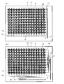
- FIG. 4A is a diagram illustrating a preferred example of the plating process
- FIG. 4B is a diagram illustrating a comparative example.
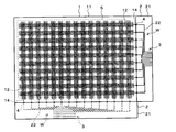
- a plurality of sensor channels 12 and a plating bus line 5 electrically connected to the plurality of sensor channels 12 are formed.
- a sensor substrate precursor 1 ′ is prepared.
- the plating bus line 5 is provided in common to the plurality of sensor channels 12 on the front and back of the sensor substrate precursor 1 ′. Each sensor channel 12 is connected to the plating bus line 5 through a plating lead wire 14 ′ connected to one end of the sensor channel 12.
- the plurality of lead-out wirings 14 ′ corresponding to the plurality of sensor channels 12 can be designed to optimize the plating process.
- the lengths of the plurality of lead-out wirings 14 ′ are equal. It is designed to be. As a result, the resistance values of the plurality of lead-out wirings 14 ′ are equal.
- the sensor channel 12 When the sensor channel 12 is subjected to plating, at least a region of the sensor base material precursor 1 ′ where the sensor channel 12 is provided is immersed in a plating bath (not shown) provided with an anode, and a plating bath is provided. Line 5 is connected to the cathode (not shown). Thus, power is supplied from the plating bus line 5 to the plurality of sensor channels 12 via the lead-out wiring 14 'for plating, and the plurality of sensor channels 12 are subjected to electrolytic plating. A plating film is formed on the sensor channel 12 by electrolytic plating. In this embodiment, since the sensor channel 12 is composed of the plurality of conductive thin wires 13, a plating film can be formed on the conductive thin wires 13 by electrolytic plating.
- the resistance values of the plurality of lead-out wirings 14 ′ are equal, the currents supplied from the bus line 5 to the plurality of sensor channels 12 through the plurality of lead-out wirings 14 ′ are made uniform, and the plurality of sensor channels 12.
- the amount of plating (the thickness of the plating film) applied to is also made uniform. Thereby, generation
- the standard deviation of the average line width variation of the plurality of conductive thin wires 13 constituting the plurality of sensor channels 12 can be reduced, and the standard deviation can be preferably 0.5 or less. .
- the standard deviation of the average resistance variation of the plurality of sensor channels 12 can be reduced, and the standard deviation can be preferably 1 or less. This effect is exhibited not only when the sensor channel 12 is formed by the plurality of conductive thin wires 13 but also when the sensor channel 12 is formed of a solid film of a conductive material, for example.
- the sensor channel 12 is composed of the conductive thin wires 13 as shown in FIG. 2, it is possible to prevent some of the conductive thin wires 13 from becoming excessively thick by preventing the occurrence of uneven plating. Thus, it is possible to satisfactorily maintain the effect that the sensor channel 12 is hardly visible.
- the sensor base material precursor 1 ' is cut along the alternate long and short dash line C, and the region where the plating bus line 5 is provided is cut out of the sensor base material precursor 1'. In this way, a sensor substrate 1 similar to that shown in FIG. 1 can be manufactured.
- the excision of the area where the plating bus line 5 is provided is preferably performed so as to cut the lead-out wiring 14 '. Thereby, a part of the lead-out wiring 14 ′ for plating can be left at the end of the sensor channel 12. A part of the lead-out wiring 14 ′ remaining on the sensor base 1 can be used as the conductor 14 shown in FIG. 1 and can be used for connection to the wiring base 2.
- the comparative example of FIG. 4B shows a case where the sensor channel 12 and the wiring 22 are provided on one base material 101.
- a plating bus line 5 connected to a wiring 22 connected to one end of the sensor channel 12 is provided in order to perform electrolytic plating on the plurality of sensor channels 12.
- the plating bus line 5 is provided so as to be in contact with the ends of the plurality of wirings 22 so that the wirings 22 are not damaged when the plating bus lines 5 are removed later.
- the lengths of the plurality of wirings 22 vary for each wiring 22. That is, the wiring 22 provided in the sensor channel 12 close to the connection site 3 is relatively short, and the wiring 22 provided in the sensor channel 12 far from the connection site 3 is relatively long. As a result, the resistance values of the plurality of wirings 22 vary due to variations in length.
- the occurrence of uneven plating cannot be prevented, and there is a limit to the improvement of sensor sensitivity.
- the sensor channel 12 is composed of the conductive thin wires 13 as shown in FIG. 2, some of the conductive thin wires 13 become excessively thick due to the occurrence of uneven plating, and the sensor channels 12 are easily visible. turn into.
- the sensor channel and the wiring may be subjected to a plurality of times of plating processes using different plating metals.
- a plurality of metal layers can be laminated on the conductive material constituting the sensor channel and the wiring by a plurality of plating processes.
- a long sensor substrate precursor 1 ′ wound in a roll shape is used, and the sensor substrate precursor 1 ′ drawn from the upstream roll is conveyed to a plating apparatus.
- the sensor substrate precursor 1 ′ that has been subjected to the plating treatment can be wound on a downstream roll.
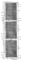
- FIG. 5 is a diagram for explaining an example of the sensor base material precursor 1 ′ used for the roll-to-roll process.
- the sensor base material precursor 1 ′ has a plurality of sensor pattern portions S constituted by a plurality of sensor channels on the long base material 11. A plurality of sensor pattern portions S are arranged along the longitudinal direction of the sensor substrate precursor 1 ′.
- the plating bus line 5 extends along the longitudinal direction of the sensor substrate precursor 1 ′.
- a lead-out wiring 14 ′ extends directly from the plating bus line 5 extending in the longitudinal direction and is connected to the sensor channel 12.
- the lead-out wiring 14 ′ extends from the plating bus line 5 branched from the plating bus line 5 extending in the longitudinal direction. It is connected to the.
- FIG. 6A shows a state in which the plating apparatus is viewed in plan
- FIG. 6B shows a state in which the plating apparatus is viewed from the side.
- 6 is a plating bath
- 7 is an anode
- 8 is a cathode roll constituting a cathode
- 9 is a transport roll.
- the plating apparatus uses a sensor substrate precursor 1 ′ similar to that shown in FIG. 5 on both sides of the sensor substrate precursor 1 ′ while being conveyed over a plurality of transfer rolls 9 in a predetermined transfer direction ⁇ .
- a voltage is applied to the anodes 7, 7 and the cathode rolls 8, 8 arranged in the above from a power supply device (not shown), and the sensor channel 12 of the sensor base precursor 1 ′ is electroplated in the plating bath 6. ing.
- the sensor base material precursor 1 ′ has a long shape as described above.
- the sensor base material precursor 1 ′ is drawn out from a roll-shaped wound body (not shown) and is wound around a plurality of transport rolls 9.
- the two cathode rolls 8 and 8 sandwich the sensor base precursor 1 ′ and are electrically connected to the plating bus lines 5 (not shown in FIG. 6) on both sides of the sensor base precursor 1 ′. In contact with each other. As a result, power can be supplied from the plating bus line 5 and electrolytic plating can be applied to the sensor channel 12 via the lead-out wiring 14 '(not shown in FIG. 6).
- electroplating is performed on both surfaces of the sensor base precursor 1 ', it is preferable to provide anodes 7 and 7 on both sides of the sensor base precursor 1' as shown in FIG.
- the cathode roll 8 is preferably disposed on the downstream side of the plating bath 6, but is not limited thereto.
- the cathode roll 8 may be provided at any position as long as it can contact the plating bus line 5.
- the cathode roll 8 may be disposed on the upstream side of the plating bath 6 or may be disposed in the plating bath 6.
- the cathode does not necessarily have to be in the form of a roll, and can have various forms that can come into contact with the plating bus line 5 on the sensor substrate precursor 1 ′.
- the plating apparatus shown in FIG. 6 is configured to vertically convey the sensor substrate precursor 1 ′, it is not limited to this.
- the electrolytic plating apparatus may transport the sensor substrate precursor 1 'horizontally.
- the plating apparatus shown in FIG. 6 is configured to perform electrolytic plating in a continuous manner while conveying the sensor substrate precursor 1 ', but is not limited thereto.
- the electrolytic plating apparatus does not necessarily have a transport mechanism, and may be configured to perform electrolytic plating in a batch manner.
- the sensor base precursor 1 ' is cut along the alternate long and short dash line C shown in FIG. 5, and the region where the plating bus line 5 is provided is cut out from the sensor base precursor 1'. In this way, a plurality of sensor substrates 1 similar to those shown in FIG. 1 can be produced from one sensor substrate precursor 1 ′.
- the plating bus line 5 is provided in order to perform power feeding for plating along the longitudinal direction of the elongated sensor base material precursor 1 ′ has been mainly shown, but the present invention is not limited to this. .
- no plating bus line is provided for the plurality of sensor channels 12 on the surface of the sensor substrate precursor 1 ′.
- a plurality of wirings 14 ′ for plating are arranged in a one-to-one relationship between a plurality of sensor channels 12 constituting one sensor pattern portion S and a plurality of sensor channels 12 constituting another sensor pattern portion S. It is provided as a plurality of bridge wirings that are electrically connected.
- a power feeding route through the plating wiring 14 ′ is formed along the longitudinal direction of the long sensor substrate precursor 1 ′ so that the above-described plating process by the roll-to-roll process can be suitably applied. become.
- the lead-out wiring 14 ′ for plating may have a planar conductive pattern 15.
- the description of the pattern constituting the sensor channel 12 is incorporated.
- planar conductive pattern 15 By providing the planar conductive pattern 15, it is possible to shorten the length of the portion provided in a straight line in the lead-out wiring 14 ′ for plating.
- the shape of the straight lead-out wiring 14 ′ for plating is greatly different from the shape of the sensor channel 12, but the shape of the planar conductive pattern 15 can be close to the shape of the sensor channel 12.
- the sensor channels 12 and the lead wires 14 ′ for plating are alternately arranged along the longitudinal direction of the elongated sensor substrate precursor 1 ′, the change in shape becomes small, particularly the sensor. Plating is also easily applied to the end of the channel 12.
- the plurality of sensor channels 12 constituting one sensor pattern portion S and the plurality of sensor channels 12 constituting the other sensor pattern portion S are individually electrically connected one-on-one.
- the present invention is not limited to this. It is not always necessary to individually handle the plurality of sensor channels 12 during the plating process.
- the planar conductive pattern 15 shown in FIG. 8 is connected to each of the plurality of lead wirings 14 ′ for plating. You may form in a wide range so that it may contact.
- the planar conductive pattern 15 is formed so as to be in direct contact with each of the plurality of sensor channels 12 constituting one of the sensor pattern portions S of the sensor pattern portions S connected to each other.
- the plurality of sensor channels 12 are connected to each other.
- the flowing current can be made uniform, and plating can be applied uniformly.
- the long sensor base precursor 1 ′ is plated by the roll-to-roll process.
- the configuration described here is a wiring base precursor for manufacturing the wiring base.
- the body can also be used as appropriate.
- FIG. 10 is a diagram illustrating an example of a wiring substrate precursor suitable for roll-to-roll processing.
- the wiring base material precursor 2 ′ has a plurality of lead wiring pattern portions W constituted by a plurality of wirings 22 on the long base material 21.
- a plurality of lead wiring pattern portions W are arranged along the longitudinal direction of the wiring substrate precursor 2 ′.
- a plurality (two in the illustrated example) of the lead wiring pattern portions W are also arranged in the width direction of the wiring base material precursor 2 ′.
- Wirings 22 constituting the lead wiring pattern portion W adjacent in the width direction are connected to each other at one end thereof.
- the plating bus line 5 extends along the longitudinal direction of the wiring substrate precursor 2 ′ and is connected to the other ends of the plurality of wirings 22 constituting the plurality of lead wiring pattern portions W.
- Such a wiring substrate precursor 2 ′ can be suitably plated by a roll-to-roll process, similarly to the sensor substrate precursor 1 ′.
- manufacturing efficiency can be improved by manufacturing at least one or more selected from the sensor channel of the sensor substrate and the wiring of the wiring substrate by roll-to-roll processing. .
- the plating process is performed as the roll-to-roll process is mainly shown, but the present invention is not limited to this.
- a patterning device for patterning a conductive material for forming the sensor channel 12 and the wiring 22 or a baking device for baking the patterned conductive material, etc. upstream of the plating device.
- the plating apparatus is not essential and may be omitted as appropriate.
- a single wiring substrate 2 is used for a plurality of sensor channels 12 provided on the surface of the sensor substrate 1, and a plurality of sensor channels 12 provided on the back surface of the sensor substrate 1 are used.
- the case of using one wiring substrate 2 is mainly shown, but the present invention is not limited to this.
- a plurality of wiring substrates 2 may be used for a plurality of sensor channels 12 provided on the front surface of the sensor substrate 1 or for a plurality of sensor channels 12 provided on the back surface of the sensor substrate 1.
- two wiring bases 2 are used for a plurality of sensor channels 12 provided on the surface of the sensor base 1, and a plurality of bases are provided on the back surface of the sensor base 1.
- Two wiring substrates 2 are also used for the sensor channel 12.
- each wiring substrate 2 is divided in the direction in which the plurality of sensor channels 12 to be connected are arranged in parallel, the wiring substrate 2 is further reduced in comparison with the first embodiment, and handling when connecting to external connection components And handling properties in the cutting process are further improved. Even if the sensor substrate 1 becomes large, the wiring substrate 2 can be kept small by increasing the number of divisions of the wiring substrate 2.
- each wiring substrate 2 may be provided with a part of the wirings 22 corresponding to a part of the sensor channels 12 among the plurality of sensor channels 12 to be connected. That is, since the number of wirings 22 provided on the wiring substrate 2 can be reduced, the space required for arranging a plurality of wirings 22 in parallel is also reduced. Thereby, not only the wiring base material 2 can be reduced in the juxtaposition direction of the plurality of sensor channels 12 to which the wiring base material 2 is connected, but also the direction orthogonal to the juxtaposition direction (longitudinal direction of the sensor channel 12). Can also be small. Since the wiring substrate 2 becomes smaller in the longitudinal direction of the sensor channel 12, not only the handling property is further improved, but also a narrow frame can be achieved.
- FIG. 11 the case where a plurality of divided wiring base materials 2 are arranged in parallel on one end side of the sensor channel 12 is shown, but the present invention is not limited to this.
- a plurality of divided wiring base materials 2 are connected to the sensor base material 1 so as to be alternately arranged on one end side and the other end side of the sensor channel 12. Also good.
- the division of the wiring substrate 2 improves the degree of freedom of the arrangement of the wiring substrate 2 (attachment position with respect to the sensor substrate 1).
- the touch panel sensor can be designed with a higher degree of freedom so that the optimum incorporation is realized.
- the plurality of sensor substrates 1 are coupled so that the sensor channels 12 are electrically connected to each other. It is preferable.
- a plurality of sensor channels 12 on one side (here, the back side) of the sensor channels 12 on the front and back sides of the sensor substrate 1 are arranged in the longitudinal direction of the sensor channel 12 (vertical direction in FIG. 13).
- the plurality of sensor channels 12 of each sensor base material 1 are electrically connected to each other so as to extend. In this way, the effective area for sensing in the touch panel sensor can be expanded.
- the sensor channels 12 of the plurality of sensor substrates 1 When the sensor channels 12 of the plurality of sensor substrates 1 are electrically connected to each other, the sensor channels 12 may be directly connected to each other, but the same as described for the connection between the sensor channel 12 and the wiring 22 It is preferable to connect via the conductor 14. By connecting through the conductor 14, a short circuit or the like can be prevented.
- the conductor 14 When providing the conductor 14, as shown in FIG. 13, the conductor 14 can be provided in the sensor channel 12 of both sensor base materials 1 of the sensor base material 1 connected to each other. In this case, the electrical connection can be reliably performed by providing the conductive member 4 so as to contact both the conductors 14.
- the conductive member 4 As the conductive member 4, the same material as described for the connection between the sensor channel 12 and the wiring 22 can be used.
- a conductor may be provided only in the sensor channel of one of the sensor substrates connected to each other. In this case, electrical connection can be reliably performed by providing the conductive member so as to contact the conductor of one sensor base and the sensor channel of the other sensor base.
- the wiring 22 of the wiring base 2 that is electrically connected to the sensor channel 12 on the surface of the sensor base 1 is disposed on the surface of the wiring base 2.
- the connection part 3 of the external connection component in 2 is arranged on the surface of the wiring substrate 2.
- the wiring 22 of the wiring base 2 that is electrically connected to the sensor channel 12 on the back surface of the sensor base 1 is connected to the wiring via a through-hole 23 provided so as to penetrate the wiring base 2. It is pulled out from the back surface of the base material 22 to the front surface. Thereby, the connection part 3 of an external connection component is arrange
- connection sites 3 of the external connection parts in the plurality of wiring base materials 2 are arranged on the same surface side.
- the present invention in order to draw out wiring from one surface of the wiring substrate to the other surface, the case of using a through hole penetrating the substrate is shown, but the present invention is not limited to this, and a known method is used. Can do. For example, a half-shaped through hole provided so as to cut out the end face of the wiring substrate may be used instead of the through hole. Further, the wiring may be folded back from one surface of the wiring substrate to the other surface at the end surface of the wiring substrate.
- connection part 3 for connecting an external connection component such as FFC or FPC is provided on the wiring substrate 2 is mainly described, but the present invention is not limited to this.
- the wiring base material 2 may be given a function as an external connection component. This will be described with reference to FIG.
- the wiring substrate 2 includes a strip-shaped portion 24 that extends from one end of the wiring substrate 2 in a strip shape.
- a plurality of aggregated wirings 22 extend to the end of the belt-like portion 24 along the longitudinal direction of the belt-like portion 24.
- Such a belt-like portion 24 can be used in place of an external connection component such as FFC or FPC, for example, and can be used to electrically connect the plurality of wirings 22 to an external circuit (not shown).
- a plurality of wirings 22 are arranged at a predetermined interval at the end of the belt-like portion 24, and this end can be connected to an external circuit provided on a circuit board (not shown).
- the end of the belt-like portion 24 preferably has a thickness sufficient to fit with the pin or the like.
- the thickness of the end of the belt-like portion 24 is insufficient, one or more films are laminated on the surface of the end opposite to the surface on which the wiring 22 is provided, and the thickness is adapted to be sandwiched by pins or the like. It is preferable to provide the thickness.
- the present invention is not limited to this.
- the belt-like portion 24 is extended from the side facing the side to which the sensor base 1 is connected in the wiring base 2 is shown, but the present invention is not limited to this.
- the belt-like portion 24 may be extended from any side of the wiring substrate 2 or may be extended from any corner of the wiring substrate 2.
- the case where the belt-like portion 24 is extended in a T shape from the wiring base material 2 is shown, but the present invention is not limited to this.
- the belt-like portion 24 may be extended from the wiring substrate 2 in an L shape.
- the strip-like portion 24 can be formed by cutting the wiring substrate 2.
- the cutting may be performed after connecting the wiring substrate 2 to the sensor substrate 1, but is preferably performed before connecting the wiring substrate 2 to the sensor substrate 1. Since the wiring substrate 2 before being connected to the sensor substrate 1 has a relatively small area, an effect of improving the handling property of cutting can be obtained.
- a plurality of (four in this example) sheet-like bodies each including a sheet-like support body 41 and a conductive member 4 supported on the support body 41 are provided. Use.
- the support 41 is not particularly limited, and for example, those exemplified as the base material of the sensor base material can be used. Similar to the sensor channel 12, the conductive member 4 is composed of a plurality of conductive thin wires arranged in a mesh shape.
- the conductive member 4 is in contact with the conductor 14 and the wiring 22 facing each other with the connection portion between the sensor base 1 and the wiring base 2 sandwiched therebetween.
- the conductive member 4 is overlaid on the connection site.
- the conductive member 4 can be fixed to the connection site by using, for example, a conductive adhesive.
- a sheet-like body composed of one support body 41 and a plurality of (four in this example) conductive members 4 supported on the support body 41 is provided. Use.
- the conductive member 4 is in contact with the conductor 14 and the wiring 22 facing each other with the connection portion between the sensor base material 1 and the wiring base material 2 interposed therebetween.
- the conductive member 4 is overlaid on the connection site.
- the plurality of conductive members 4 are arranged on the support body 41 at the same pitch as the plurality of conductors 14 or the plurality of wirings 22 so as not to contact unintended wirings.
- a conductive adhesive or the like can be used when the conductive members 4 are overlapped.
- the conductive adhesive can be used by defining an application range for each conductive member 4 on the support 41.
- the conductive member 4 may be superposed using an adhesive tape as the support 41.
- a sheet-like body including one support body 41 and a plurality (four in this example) of conductive members 4 supported on the support body 41. Is used.
- the support body 41 has an area capable of covering a part or all of the plurality of sensor channels 12.
- the support 41 can be, for example, a cover layer for protecting the sensor channel 12.
- the support 41 can be a white layer for forming an image projection surface (screen) on the sensor channel 12, for example.
- As the white layer for example, a resin layer in which a white pigment is dispersed can be used.
- an image from an image projection device (projector) (not shown) can be projected and displayed on the screen.
- a sensor film for example, a touch screen having both a sensor function and a screen function can be configured.
- the conductive member 4 is in contact with the conductor 14 and the wiring 22 facing each other across the connection portion between the sensor base 1 and the wiring base 2.
- the conductive member 4 is overlaid on the connection site.
- the support body 41 can cover a part or all of the plurality of sensor channels 12.
- the substrate 8 can cover and protect not only the sensor channel 12 but also the wiring 22.
- the end of the wiring can be exposed from the support body 41 for connection with an external connection component or the like.
- the conductive member supported on the support is constituted by a plurality of conductive thin wires, but the present invention is not limited to this.
- the conductive member may be formed in a solid shape on the support.
- the conductive member is supported on the support.
- the conductive member is made of, for example, a metal foil and has sufficient strength, the support may be omitted. Good.
- the conductive member described above can be preferably used for electrical connection between the sensor channel and the sensor channel as shown in FIG.
- the touch panel sensor substrate of the present invention has at least one sensor substrate having a sensor pattern portion composed of a plurality of sensor channels and a lead wiring pattern portion composed of a plurality of wires.
- the sensor channel of the sensor base material and the wiring of the wiring base material are electrically connected to each other.
- the touch panel sensor substrate set of the present invention can be used to configure a touch panel sensor, and includes at least one sensor substrate and at least one wiring substrate described above. By connecting the sensor substrate and the wiring substrate so that the sensor channel of the sensor substrate constituting the touch panel sensor substrate set and the wiring of the wiring substrate are electrically connected, the touch panel sensor substrate Can be manufactured.
- the touch panel sensor base material set may further include the above-described conductive member. Thereby, a touch panel sensor with good electrical connection between the sensor channel and the wiring can be efficiently manufactured.
- a conductor may be provided at both of the two ends (one end and the other end) of the sensor channel. If conductors are provided at both of the two ends of the sensor channel, a wiring substrate can be connected to both sides of the sensor substrate. In this case, the conductors provided at both of the two ends of the sensor channel can be electrically connected to the wiring of each wiring substrate. Even when the conductor is omitted, the wiring substrate can be connected to both sides of the sensor substrate. In this case, the two ends of the sensor channel can be electrically connected to the wiring of each wiring substrate.
- the present invention is not limited to this.
- the sensor substrate may have a sensor pattern part on one side.
- the sensor pattern portion having the two-layer structure can suitably perform position detection in the XY coordinate system, similarly to the sensor pattern portions on both sides described above.
- the method of making the sensor pattern part into a two-layer structure by lamination is not particularly limited as long as the insulation between the sensor pattern parts of each sensor base material to be laminated is maintained.
- lamination first, two units are prepared by connecting a sensor base material having a sensor pattern part on one side and a wiring base material to which external connection components are connected. Then, the sensor pattern part can be made into a two-layer structure by laminating two units of the sensor substrate.
- the sensor bases of the two units When stacking the sensor bases of the two units, they may be stacked so that the surfaces not provided with the sensor channels face each other, or the surface of the one sensor base not provided with the sensor channels You may laminate
- the latter form is particularly preferable, and an effect that the external connection parts can be arranged on the same surface side with respect to the wiring base material of each unit is obtained.
- the terms “front surface” and “back surface” of the base material are used for the purpose of distinguishing one surface of the base material from the other surface formed on the back side as viewed from the one surface. This is merely a description, and in a product including a touch panel sensor, it is not limited that the “front surface” is oriented to the front surface side and the “back surface” is oriented to the back surface side. In a product including a sensor film, the “front surface” may be oriented to the back surface side, and the “back surface” may be oriented to the front surface side.
- Example 1 First, a sensor substrate precursor 1 ′ similar to that shown in FIG. A plurality of thin conductive wires 13 constituting the sensor channel 12 were formed by an ink jet method. The size of the sensor pattern portion S formed by the plurality of sensor channels 12 is 60 inches (width: about 1300 mm, height: about 750 mm).
- the line width of the conductive thin wire 13 before plating and the line width of the conductive thin wire 13 after plating were measured at 10 points randomly selected from the plurality of sensor channels 12 constituting the sensor pattern portion S. These measurements, averages and standard deviations are shown in Table 1.
- the line width ( ⁇ m) of the conductive thin wire is the end in the width direction (thickness direction) of the thin wire observed with an optical microscope (Keyence Corporation “Digital Microscope VHX-5000” magnified 5000 times). It is the distance between parts.
- the sheet resistance of the sensor channel 12 after plating was measured at 10 points randomly selected from the plurality of sensor channels 12 constituting the sensor pattern portion S. These measurements, averages and standard deviations are shown in Table 2.
- the sheet resistance ( ⁇ / ⁇ ) is a value measured using “Loresta-AX” manufactured by Mitsubishi Chemical Analytech.
- Example 1 A sensor substrate precursor 101 similar to that shown in FIG. The sensor pattern portion S was formed in the same manner as in Example 1.
- the line width of the conductive thin wire 13 before plating and the line width of the conductive thin wire 13 after plating were measured at 10 points randomly selected from the plurality of sensor channels 12 constituting the sensor pattern portion S. These measurements, averages and standard deviations are shown in Table 1.
- the sheet resistance of the sensor channel 12 after plating was measured at 10 points randomly selected from the plurality of sensor channels 12 constituting the sensor pattern portion S. These measurements, averages and standard deviations are shown in Table 2.
- Example 2 A long sensor substrate precursor 1 ′ similar to that shown in FIG. 5 was prepared.
- a plurality of thin conductive wires 13 constituting the sensor channel 12 were formed by an ink jet method.
- the size of the sensor pattern portion S formed by the plurality of sensor channels 12 is 60 inches (width: about 1300 mm, height: about 750 mm). Five sensor pattern portions S were formed along the longitudinal direction of the sensor substrate precursor 1 ′.
- a plurality of sensor channels 12 are connected from the plating bus line 5 of the sensor base precursor 1 ′ via the plurality of lead-out wirings 14 ′. Power was supplied and electrolytic plating (copper plating) was performed in a copper plating bath.
- the line width of the conductive thin wire 13 before plating was measured at 10 locations randomly selected from the plurality of sensor channels 12. The measured values were substantially the same in the other four sensor pattern portions S. Further, for each of the five sensor pattern portions S (Nos. 1 to 5), the line widths of the conductive thin wires 13 after plating were measured at 10 points randomly selected from the plurality of sensor channels 12. Furthermore, the sheet resistance of the sensor channel 12 after plating was measured at 10 points selected at random. These measurements, averages and standard deviations are shown in Table 3.
- Example 3 The sensor base material precursor 1 ′ plated in Example 1 was cut along the alternate long and short dash line C shown in FIG. 4A to obtain the same sensor base material 1 as shown in FIG. .
- the obtained sensor substrate 1 was connected to the same wiring substrate 2 as shown in FIG. At that time, the conductor 14 extending from the sensor channel 12 of the sensor base 1 and the wiring 22 of the wiring base 2 were connected by the conductive member 4.
Landscapes
- Engineering & Computer Science (AREA)
- General Engineering & Computer Science (AREA)
- Theoretical Computer Science (AREA)
- Human Computer Interaction (AREA)
- Physics & Mathematics (AREA)
- General Physics & Mathematics (AREA)
- Position Input By Displaying (AREA)
Abstract
本発明は、特に大面積のタッチパネルセンサー基材を製造する場合においても、タッチパネルセンサー基材の品質を向上でき、また歩留りも向上できるタッチパネルセンサー基材の製造方法及びタッチパネルセンサー基材セットを提供することを課題とし、当該課題は、複数のセンサーチャネル(12)からなるセンサーパターン部(S)を有する少なくとも1つのセンサー基材(1)と、複数の配線(22)からなる引出配線パターン部(W)を有する少なくとも1つの配線基材(2)とを用意し、次いで、センサー基材(1)のセンサーチャネル(12)と配線基材(2)の配線(22)とが電気的に接続されるように、センサー基材(1)と配線基材(2)とを接続するタッチパネルセンサー基材の製造方法により解決される。
Description
本発明は、タッチパネルセンサー基材の製造方法及びタッチパネルセンサー基材セットに関し、より詳しくは、特に大面積のタッチパネルセンサー基材を製造する場合においても、タッチパネルセンサー基材の品質を向上でき、また歩留りも向上できるタッチパネルセンサー基材の製造方法及びタッチパネルセンサー基材セットに関する。
タッチパネルセンサーは、例えば携帯端末等に搭載され、ユーザーによってタッチされた位置を検出するために利用されている。
特許文献1、2には、画像表示装置に関して、表示される画像を大面積化する技術が提案されている。しかし、タッチパネルセンサーに関しては、携帯端末のような比較的小型の装置に搭載されることが多いため、面積を大きくするための技術は十分に確立されていない。
従来、タッチパネルセンサー基材を製造する際には、1つの基材上にセンサーチャネルと該センサーチャネルに接続される引出配線とを形成していた。
かかる従来技術には、特に大面積のタッチパネルセンサー基材を製造する場合に、品質向上の観点、及び、歩留りを向上する観点で、更なる改善の余地が見出された。
そこで本発明の課題は、特に大面積のタッチパネルセンサー基材を製造する場合においても、タッチパネルセンサー基材の品質を向上でき、また歩留りも向上できるタッチパネルセンサー基材の製造方法及びタッチパネルセンサー基材セットを提供することにある。
また本発明の他の課題は、以下の記載によって明らかとなる。
上記課題は、以下の各発明によって解決される。
1.
複数のセンサーチャネルからなるセンサーパターン部を有する少なくとも1つのセンサー基材と、複数の配線からなる引出配線パターン部を有する少なくとも1つの配線基材とを用意し、
次いで、前記センサー基材の前記センサーチャネルと前記配線基材の前記配線とが電気的に接続されるように、前記センサー基材と前記配線基材とを接続するタッチパネルセンサー基材の製造方法。
2.
前記複数のセンサーチャネルと前記複数の配線とが1対1に対応するように前記センサー基材と前記配線基材とを配置し、
次いで、前記センサー基材の前記センサーチャネルと前記配線基材の前記配線とを導電部材によって電気的に接続する前記1記載のタッチパネルセンサー基材の製造方法。
3.
前記センサー基材の前記センサーチャネル、及び、前記配線基材の前記配線から選ばれる少なくとも1つ以上を、めっき処理を施して製造する前記1又は2記載のタッチパネルセンサー基材の製造方法。
4.
前記めっき処理が電解めっきである前記3記載のタッチパネルセンサー基材の製造方法。
5.
複数のセンサーチャネルと、前記複数のセンサーチャネルに対して電気的に接続されためっき用バスラインとが形成されたセンサー基材前駆体を用意し、
次いで、前記めっき用バスラインを介して前記複数のセンサーチャネルに給電することによって、前記複数のセンサーチャネルに電解めっきを施し、
次いで、前記センサー基材前駆体のうち前記めっき用バスラインが設けられた領域を切除して、前記センサー基材を製造する前記4記載のタッチパネルセンサー基材の製造方法。
6.
前記センサー基材の前記センサーチャネル、及び、前記配線基材の前記配線から選ばれる少なくとも1つ以上を、インクジェット法により形成した後、めっき処理を施して製造する前記3~5の何れかに記載のタッチパネルセンサー基材の製造方法。
7.
前記センサー基材の前記センサーチャネルの製法と、前記配線基材の前記配線の製法とが異なる前記1~6の何れかに記載のタッチパネルセンサー基材の製造方法。
8.
前記配線基材の前記配線をレーザー処理により製造する前記1~7の何れかに記載のタッチパネルセンサー基材の製造方法。
9.
前記配線基材の前記配線をフォトリソグラフィー処理により製造する前記1~7の何れかに記載のタッチパネルセンサー基材の製造方法。
10.
前記配線基材の前記配線をスクリーン印刷処理により製造する前記1~7の何れかに記載のタッチパネルセンサー基材の製造方法。
11.
前記センサー基材の前記センサーチャネル、及び、前記配線基材の前記配線から選ばれる少なくとも1つ以上を、ロールtoロール処理により製造する前記1~10の何れかに記載のタッチパネルセンサー基材の製造方法。
12.
前記センサー基材は前記センサーパターン部を両面に有する前記1~11の何れかに記載のタッチパネルセンサー基材の製造方法。
13.
前記配線基材は該配線基材の一端部から帯状に延設された帯状部を備え、
前記帯状部には、前記複数の配線が、該帯状部の長手方向に沿って該帯状部の末端まで伸びている前記1~12の何れかに記載のタッチパネルセンサー基材の製造方法。
14.
前記配線基材を前記センサー基材に接続する前に、前記帯状部を形成するように前記配線基材を裁断する前記13記載のタッチパネルセンサー基材の製造方法。
15.
タッチパネルセンサーを構成するための基材セットであって、
複数のセンサーチャネルからなるセンサーパターン部を有する少なくとも1つのセンサー基材と、
複数の配線からなる引出配線パターン部を有する少なくとも1つの配線基材と、によって構成されたタッチパネルセンサー基材セット。
16.
前記センサー基材の前記センサーチャネルは複数の導電性細線によって構成され、
前記複数の導電性細線の平均線幅バラツキが標準偏差0.5以下である前記15記載のタッチパネルセンサー基材セット。
17.
前記センサー基材の同一面上に設けられた前記複数のセンサーチャネルの平均抵抗バラツキが標準偏差1以下である前記15又は16記載のタッチパネルセンサー基材セット。
18.
前記センサー基材の前記センサーチャネルはめっき皮膜を有する前記15~17の何れかに記載のタッチパネルセンサー基材セット。
19.
前記センサー基材の前記センサーチャネルと前記配線基材の前記配線とが導電部材によって電気的に接続されている前記15~18の何れかに記載のタッチパネルセンサー基材セット。
20.
前記センサー基材は前記センサーパターン部を両面に有する前記15~19の何れかに記載のタッチパネルセンサー基材セット。
複数のセンサーチャネルからなるセンサーパターン部を有する少なくとも1つのセンサー基材と、複数の配線からなる引出配線パターン部を有する少なくとも1つの配線基材とを用意し、
次いで、前記センサー基材の前記センサーチャネルと前記配線基材の前記配線とが電気的に接続されるように、前記センサー基材と前記配線基材とを接続するタッチパネルセンサー基材の製造方法。
2.
前記複数のセンサーチャネルと前記複数の配線とが1対1に対応するように前記センサー基材と前記配線基材とを配置し、
次いで、前記センサー基材の前記センサーチャネルと前記配線基材の前記配線とを導電部材によって電気的に接続する前記1記載のタッチパネルセンサー基材の製造方法。
3.
前記センサー基材の前記センサーチャネル、及び、前記配線基材の前記配線から選ばれる少なくとも1つ以上を、めっき処理を施して製造する前記1又は2記載のタッチパネルセンサー基材の製造方法。
4.
前記めっき処理が電解めっきである前記3記載のタッチパネルセンサー基材の製造方法。
5.
複数のセンサーチャネルと、前記複数のセンサーチャネルに対して電気的に接続されためっき用バスラインとが形成されたセンサー基材前駆体を用意し、
次いで、前記めっき用バスラインを介して前記複数のセンサーチャネルに給電することによって、前記複数のセンサーチャネルに電解めっきを施し、
次いで、前記センサー基材前駆体のうち前記めっき用バスラインが設けられた領域を切除して、前記センサー基材を製造する前記4記載のタッチパネルセンサー基材の製造方法。
6.
前記センサー基材の前記センサーチャネル、及び、前記配線基材の前記配線から選ばれる少なくとも1つ以上を、インクジェット法により形成した後、めっき処理を施して製造する前記3~5の何れかに記載のタッチパネルセンサー基材の製造方法。
7.
前記センサー基材の前記センサーチャネルの製法と、前記配線基材の前記配線の製法とが異なる前記1~6の何れかに記載のタッチパネルセンサー基材の製造方法。
8.
前記配線基材の前記配線をレーザー処理により製造する前記1~7の何れかに記載のタッチパネルセンサー基材の製造方法。
9.
前記配線基材の前記配線をフォトリソグラフィー処理により製造する前記1~7の何れかに記載のタッチパネルセンサー基材の製造方法。
10.
前記配線基材の前記配線をスクリーン印刷処理により製造する前記1~7の何れかに記載のタッチパネルセンサー基材の製造方法。
11.
前記センサー基材の前記センサーチャネル、及び、前記配線基材の前記配線から選ばれる少なくとも1つ以上を、ロールtoロール処理により製造する前記1~10の何れかに記載のタッチパネルセンサー基材の製造方法。
12.
前記センサー基材は前記センサーパターン部を両面に有する前記1~11の何れかに記載のタッチパネルセンサー基材の製造方法。
13.
前記配線基材は該配線基材の一端部から帯状に延設された帯状部を備え、
前記帯状部には、前記複数の配線が、該帯状部の長手方向に沿って該帯状部の末端まで伸びている前記1~12の何れかに記載のタッチパネルセンサー基材の製造方法。
14.
前記配線基材を前記センサー基材に接続する前に、前記帯状部を形成するように前記配線基材を裁断する前記13記載のタッチパネルセンサー基材の製造方法。
15.
タッチパネルセンサーを構成するための基材セットであって、
複数のセンサーチャネルからなるセンサーパターン部を有する少なくとも1つのセンサー基材と、
複数の配線からなる引出配線パターン部を有する少なくとも1つの配線基材と、によって構成されたタッチパネルセンサー基材セット。
16.
前記センサー基材の前記センサーチャネルは複数の導電性細線によって構成され、
前記複数の導電性細線の平均線幅バラツキが標準偏差0.5以下である前記15記載のタッチパネルセンサー基材セット。
17.
前記センサー基材の同一面上に設けられた前記複数のセンサーチャネルの平均抵抗バラツキが標準偏差1以下である前記15又は16記載のタッチパネルセンサー基材セット。
18.
前記センサー基材の前記センサーチャネルはめっき皮膜を有する前記15~17の何れかに記載のタッチパネルセンサー基材セット。
19.
前記センサー基材の前記センサーチャネルと前記配線基材の前記配線とが導電部材によって電気的に接続されている前記15~18の何れかに記載のタッチパネルセンサー基材セット。
20.
前記センサー基材は前記センサーパターン部を両面に有する前記15~19の何れかに記載のタッチパネルセンサー基材セット。
本発明によれば、特に大面積のタッチパネルセンサー基材を製造する場合においても、タッチパネルセンサー基材の品質を向上でき、また歩留りも向上できるタッチパネルセンサー基材の製造方法及びタッチパネルセンサー基材セットを提供することができる。
以下に、本発明を実施するための形態について詳しく説明する。
本発明のタッチパネルセンサー基材の製造方法では、複数のセンサーチャネルからなるセンサーパターン部を有する少なくとも1つのセンサー基材と、複数の配線からなる引出配線パターン部を有する少なくとも1つの配線基材とを用意し、次いで、前記センサー基材の前記センサーチャネルと前記配線基材の前記配線とが電気的に接続されるように、前記センサー基材と前記配線基材とを接続する。これにより、特に大面積のタッチパネルセンサー基材を製造する場合においても、タッチパネルセンサー基材の品質を向上でき、また歩留りも向上できる効果が得られる。
1.第1実施形態
第1実施形態に係るタッチパネルセンサー製造方法について、図1~図4を参照して説明する。本実施形態では、まず、図1に示すように、センサー基材1及び配線基材2を用意する。
第1実施形態に係るタッチパネルセンサー製造方法について、図1~図4を参照して説明する。本実施形態では、まず、図1に示すように、センサー基材1及び配線基材2を用意する。
〔センサー基材〕
センサー基材1は、基材11と、該基材11上に設けられた複数のセンサーチャネル12とによって構成されている。複数のセンサーチャネル12によってセンサーパターン部Sが構成される。センサーパターン部Sは、タッチパネルセンサーにおいてセンシングに有効な領域を形成する。
センサー基材1は、基材11と、該基材11上に設けられた複数のセンサーチャネル12とによって構成されている。複数のセンサーチャネル12によってセンサーパターン部Sが構成される。センサーパターン部Sは、タッチパネルセンサーにおいてセンシングに有効な領域を形成する。
〔基材〕
基材11は、複数のセンサーチャネル12を互いに絶縁された状態で表面に保持できるものであればよく、例えば樹脂基材(フィルムともいう)、ガラス基材、セラミック基材等が挙げられる。
基材11は、複数のセンサーチャネル12を互いに絶縁された状態で表面に保持できるものであればよく、例えば樹脂基材(フィルムともいう)、ガラス基材、セラミック基材等が挙げられる。
フィルムの材質は格別限定されず、例えば、ポリエチレンテレフタレート(PET)樹脂、ポリエチレンナフタレート(PEN)樹脂、ポリブチレンテレフタレート樹脂、セルロース系樹脂(ポリアセチルセルロース、セルロースジアセテート、セルローストリアセテート等)、ポリエチレン樹脂、ポリプロピレン系樹脂、メタクリル系樹脂、環状ポリオレフィン系樹脂、ポリスチレン系樹脂、アクリロニトリル-(ポリ)スチレン共重合体(AS樹脂)、アクリロニトリル-ブタジエン-スチレン共重合体(ABS樹脂)、ポリ塩化ビニル系樹脂、ポリ(メタ)アクリル系樹脂、ポリカーボネート系樹脂、ポリエステル系樹脂、ポリイミド系樹脂、ポリアミド系樹脂、ポリアミドイミド系樹脂、シクロオレフィンポリマー(COP)樹脂等が挙げられる。これらの材質を用いれば、フィルムに良好な絶縁性と透明性を付与できる。また、特に合成樹脂材料を用いることによって、フィルムに良好な可撓性を付与することができる。合成樹脂材料により構成されたフィルムは、延伸されていても、未延伸であってもよい。
基材11の厚さは格別限定されず、例えば1μm~10cm程度、更には20μm~300μm程度とすることができる。
基材11には、表面エネルギーを変化させる表面処理が施されていてもよい。更に、基材11は、積層体でもよく、ハードコート層や反射防止層などを有してもよい。
本実施形態において基材11は長方形であるが、基材11の形状はこれに限定されず、任意の形状を付与できる。
〔センサーチャネル〕
本実施形態において、センサーチャネル12は、タッチパネルセンサーにおいてタッチを検出するための電極である。タッチパネルセンサーの検出方式は格別限定されず、例えば、抵抗膜方式、静電容量方式、光センサー方式等が挙げられる。
本実施形態において、センサーチャネル12は、タッチパネルセンサーにおいてタッチを検出するための電極である。タッチパネルセンサーの検出方式は格別限定されず、例えば、抵抗膜方式、静電容量方式、光センサー方式等が挙げられる。
センサーパターン部Sには、複数のセンサーチャネル12が等ピッチで配置されている。
センサーチャネル12は導電性材料によって所定の幅(チャネル幅ともいう)を有する帯状に形成されている。センサーチャネル12の長さや幅は格別限定されず、目的、用途等に応じて適宜設定できる。
センサーチャネル12を構成する導電性材料は格別限定されないが、金属微粒子、金属酸化物微粒子、カーボン微粒子、導電性ポリマー等が挙げられる。金属微粒子を構成する金属として、例えば、Au、Pt、Ag、Cu、Ni、Cr、Rh、Pd、Zn、Co、Mo、Ru、W、Os、Ir、Fe、Mn、Ge、Sn、Ga、In等が挙げられる。これらの中でも、Au、Ag、Cuが好ましく、Agが特に好ましい。金属微粒子の平均粒子径は、例えば1~100nm、更には3~50nmとすることができる。平均粒子径は、体積平均粒子径であり、マルバーン社製「ゼータサイザ1000HS」により測定することができる。金属酸化物微粒子として、例えば、酸化インジウムスズ(ITO)、酸化スズ等が挙げられる。カーボン微粒子としては、例えば、グラファイト微粒子、カーボンナノチューブ、フラーレン等が挙げられる。導電性ポリマーとしては、格別限定されないが、π共役系導電性高分子を好ましく挙げることができる。π共役系導電性高分子としては、例えば、ポリチオフェン類やポリアニリン類等が挙げられる。π共役系導電性高分子は、例えばポリスチレンスルホン酸等のようなポリアニオンと共に用いてもよい。
センサーチャネル12は基材11上にベタ状に付与された導電性材料によって構成されてもよいが、本実施形態においてセンサーチャネル12は、図2(a)に示すように、基材11上に2次元的に配置された複数の導電性細線13によって構成されている。
図2(a)に示すセンサーチャネル12は、複数の導電性細線13からなるメッシュパターンによって構成されている。この例に限定されず、センサーチャネル12のパターンは、例えばストライプパターン、ランダムパターン等であってもよい。
また、センサーチャネルのパターンは、幾何学図形を成す導電性細線を複数組み合わせて構成されたパターンであってもよい。幾何学図形を成す導電性細線を複数組み合わせて構成されたパターンからなるセンサーチャネルの一例について図2(b)に示す。
図2(b)の例において、センサーチャネル12は、四角形を成す複数の導電性細線13によって構成されている。センサーチャネル12のパターンは、四角形の2本の対角線の方向に、四角形を成す導電性細線13を二次元的に複数並設することによって構成されている。
センサーチャネル12を構成する導電性細線13の線幅は格別限定されないが、例えば50μm以下、20μm以下とすることができ、好ましくは10μm以下、7μm以下、更には5μm以下とすることである。導電性細線13の線幅を10μm以下にすることによって、導電性細線13及び該導電性細線13によって構成されるパターン(ここではメッシュパターン)からなるセンサーチャネル12が視認されにくくなる効果が得られる。導電性細線13の線幅の下限は格別限定されないが、安定した導電性を付与する観点では、例えば1μm以上とすることができる。
図1に示したように、本実施形態において、センサー基材1はセンサーパターン部Sを両面に有している。即ち、センサー基材1は、基材11の両面にセンサーパターン部Sを構成する複数のセンサーチャネル12を備えている。これら両面のセンサーチャネル12は、基材11を介して対向している。本実施形態のように、1つの基材11の両面にセンサーパターン部Sを形成する場合は、基材を積層する工程を省略できる効果が得られる。また、後に詳述するように、片面にセンサーパターン部を有する基材を積層することによってセンサーパターン部Sを2層化することもできる。
基材11の表面のセンサーチャネル12の長手方向は基材11の長辺(図1中、横方向に配向された辺)方向と平行である。また、基材11の表面のセンサーチャネル12は、基材11の短辺(図1中、縦方向に配向された辺)方向に複数並設されている。
基材11の裏面のセンサーチャネル12の長手方向は基材11の短辺(図1中、縦方向に配向された辺)方向と平行である。また、基材11の裏面のセンサーチャネル12は、基材11の長辺(図1中、横方向に配向された辺)方向に複数並設されている。
表面のセンサーチャネル12と、裏面のセンサーチャネル12とが、互いに交差する方向に配向されることで、センサーパターン部Sにおいて、XY座標系での位置検出が可能になる。
ここでは基材11の表面に10本のセンサーチャネル12が並設され、基材11の裏面に15本のセンサーチャネル12が並設される場合について示しているが、これに限定されず、目的や用途等に応じて任意の本数のセンサーチャネル12を並設することができる。特にセンサーパターン部Sを大面積化する場合は、例えば、各面に20本以上、30本以上、更には40本以上のセンサーチャネル12を並設することができる。併設されるセンサーチャネル12の本数の上限は格別限定されないが、例えば500本以下とすることができる。
互いに隣接するセンサーチャネル12間の間隔αは格別限定されないが、例えば150μm以下、100μm以下、更には50μm以下まで小さくすることが好ましい。これにより、センサーチャネル12を密な状態で配置でき、センサー感度を向上できる。また、間隔αを、例えば30μm以下、更には25μm以下まで小さくすることも好ましい。これにより、センサー感度を向上できると共に、センサーチャネ12間の隙間(絶縁部)が視認されてしまうことを防止できる。間隔αの下限は、センサーチャネル12間を絶縁できるものであれば格別限定されないが、例えば5μm以上、10μm以上、更には15μm以上とすることで、センサーチャネル12間に埃等が付着しても絶縁状態を良好に保持できる。
センサーチャネル12を基材11の一端(後に配線基材2が接続される接続部位)まで設けてもよいが、センサーチャネル12の端部と、基材11の一端との間には間隔βを設けることが好ましい。間隔βが設けられることによって、配線基材2が接続される接続部位である基材11の一端にセンサーチャネル12が直接露出することが回避され、意図しない短絡の発生が防止される。間隔βを設ける場合、その値は格別限定されず、例えば0.5mm~10mm、更には1mm~6mmとすることができる。
〔導体〕
本実施形態において、センサー基板1は、センサーパターン部Sの外部に、センサーチャネル12の端部から基材11の一端まで伸びる導体14を備えている。基材11の一端は、後に配線基材2が接続される接続部位であり、この接続部位において複数の導体14は配線基材2の複数の配線22と電気的に接続される。
本実施形態において、センサー基板1は、センサーパターン部Sの外部に、センサーチャネル12の端部から基材11の一端まで伸びる導体14を備えている。基材11の一端は、後に配線基材2が接続される接続部位であり、この接続部位において複数の導体14は配線基材2の複数の配線22と電気的に接続される。
本実施形態において、複数の導体14は、上述した間隔βに対応する領域に、センサーチャネル12の配列ピッチと等しい配列ピッチで設けられている。
導体14は導電性材料からなり、センサーチャネル12とは異なる構造を有している。本実施形態において、導体14は、センサーチャネル12のチャネル幅より細く設けられている点で、センサーチャネル12と構造が異なっている。導体14がセンサーチャネル12と異なる構造を有する場合の例は、幅等の形状が異なる場合に限定されず、例えば、導体14がセンサーチャネル12とは異なる導電性材料によって形成されている場合や、導体14がセンサーチャネル12とは異なる抵抗値(例えばシート抵抗値)を有する場合等も含む。
本実施形態では導体14が1本の配線である場合について示しているが、これに限定されず、導体14は例えばセンサーチャネル12と同様のメッシュパターンであってもよい。また、メッシュパターンに代えて、例えば幾何学図形を成す導電性細線を複数組み合わせて構成されたパターン、ストライプパターン、ランダムパターン等の種々のパターンであってもよい。更に、導体は、パターンを有するものに限定されず、ベタ状に付与された導電性材料によって構成されてもよい。
導体14は、何れの形態であっても、センサーチャネル12のチャネル幅より細く設けられていることが好ましい。これにより、配線基材2が接続される接続部位である基材11の一端に露出する導体14が、センサーチャネル12の幅より細いことによって、該一端にセンサーチャネル12を露出させる場合との対比で、意図しない短絡の発生が防止される。
〔配線基材〕
図1に示すように、配線基材2は、基材21と、該基材21上に形成された複数の配線22とによって構成されている。複数の配線22は、センサー基材1が有する複数のセンサーチャネル12のそれぞれに電気的に接続される。複数の配線22によって、基材21上に引出配線パターン部Wが構成されている。
図1に示すように、配線基材2は、基材21と、該基材21上に形成された複数の配線22とによって構成されている。複数の配線22は、センサー基材1が有する複数のセンサーチャネル12のそれぞれに電気的に接続される。複数の配線22によって、基材21上に引出配線パターン部Wが構成されている。
本実施形態では、2つの配線基材2を用意している。一方の配線基材2は、センサー基材1の表面のセンサーチャネル12に電気的に接続される配線22を有している。他方の配線基材2は、センサー基材1の裏面のセンサーチャネル12に電気的に接続される配線22を有している。
配線基材2において、配線22の一端は基材21の一端まで伸び、該配線22の他端は基材21上の所定の位置(ここでは基材21の他端)まで伸びている。
配線22の一端が配置される基材21の一端は、後にセンサー基材1が接続される接続部位であり、この接続部位において、複数の配線22は、それぞれセンサー基材1の複数の導体14に接続され、その結果として複数の導体14を介して複数のセンサーチャネル12と電気的に接続される。センサー基材1と配線基材2との接続部位において、センサー基材1の複数の導体14の配列ピッチと、配線基材2の複数の配線22の配列ピッチとは等しい関係にある。
一方、配線22の他端が配置される基材21の他端には、後に図示しない外部接続部品が接続される接続部位3が形成される。この接続部位3において、配線22の他端は外部接続部品に電気的に接続される。外部接続部品としては、例えば、配線基材2の複数の配線22を、図示しない外部回路に電気的に接続するための部品等が挙げられ、具体的には、例えばFFCやFPC等が挙げられる。配線基材2の配線22と、外部接続部品が備える外部配線とを電気的に接続する方法は格別限定されず、例えば導電性接着剤や異方性導電フィルム(ACF)等によって接続することができる。導電性接着剤は格別限定されず、例えば導電性粒子を含有させた接着剤等を用いることができる。
配線基材2と外部接続部品との接続部位3における複数の配線22の配列ピッチは、センサー基材1と配線基材2との接続部位における配列ピッチより小さく設けられている。また、配線基材2と外部接続部品との接続部位3においては、複数の配線22の線幅及び線間隔(Line&Space;L/Sともいう)も、センサー基材1と配線基材2との接続部位におけるL/Sより狭く集約されている。
つまり、本実施形態では、引出配線パターン部Wにおいて、複数の配線22の配列ピッチやL/Sは、センサー基材1と配線基材2との接続部位において比較的大きく、配線基材2と外部接続部品との接続部位3において比較的小さい関係にある。
〔センサー基材と配線基材との接続〕
次いで、図3に示すように、センサー基材1と配線基材2とを接続する。
次いで、図3に示すように、センサー基材1と配線基材2とを接続する。
センサー基材1と配線基材2とを接続する際には、センサー基材1の一端と、配線基材2の一端とを突き合わせた状態で、センサー基材1のセンサーチャネル12と、配線基材2の配線22とを電気的に接続することができる。ここでは、複数のセンサーチャネル12と複数の配線22とが1対1に対応するようにセンサー基材1と配線基材2とを配置している。
本実施形態では、センサー基材1と配線基材2との接続部位に、複数のセンサーチャネル12から伸びる複数の導体14と、該導体14と等しい数の複数の配線22とが、互いに等しいピッチで対向するように、センサー基材1と配線基材2とを互いに位置合わせしている。このとき、センサー基材1及び配線基材2の一方又は両方に、両基材を互いに位置合わせするためのマーカー(図示省略)が付与されていてもよい。
センサーチャネル12と配線22との電気的な接続を確実にするために、接続部位に導電部材4を付与することは好ましいことである。
本実施形態のようにセンサーチャネル12に導体14が接続されている場合、導電部材4は、導体14及び配線22の両方に接触するように付与することが好ましい。導体14が省略され、センサーチャネル12がセンサー基材1の一端まで伸びている場合は、導電部材4は、センサーチャネル12及び配線22の両方に接触するように付与することができる。
導電部材4は、格別限定されず、例えば導電性ペースト(例えば金属ペースト)や導電性インク等が挙げられる。これらの付与方法は格別限定されず、例えばインクジェット法等の印刷法によって付与することができる。導電性ペーストや導電性インクは、乾燥及び又は硬化によって、導体14及び配線22の両方に接触した状態で固定できる。導電部材4の他の例については、後に詳述する。
本実施形態では、センサー基材1の両面にセンサーチャネル12が設けられているため、これら両面のセンサーチャネル12と、配線基材2の配線22とを電気的に接続するように、センサー基材1と配線基材2とが接続される。本実施形態では、センサー基材1の表面のセンサーチャネル12に対しては、表面に配線22が設けられた配線基材2の該配線22を電気的に接続し、センサー基材1の裏面のセンサーチャネル12に対しては、裏面に配線22が設けられた配線基材2の該配線22を電気的に接続することで、センサー基材1の両面のセンサーチャネル12と配線22とを電気的に接続している。
上述したように、配線基材2は図示しない外部接続部品を接続するための接続部位3を備えている。配線基材2と外部接続部品との接続は、センサー基材1と配線基材2とを接続した後に行ってもよいが、センサー基材1と配線基材2とを接続する前に行うことが好ましい。センサー基材1と接続される前の配線基材2は比較的小面積であるため、外部接続部品を接続する際のハンドリング性に優れ、高精度な接続を実現できるからである。
本実施形態では、センサー基材1と配線基材2とを別体として用意しているため、以下に説明するように、歩留り向上の効果が得られる。
まず、従来の技術では、1つの基材上にセンサーパターン部と引出配線パターン部とを形成していたが、この場合、センサーパターン部が良品であっても、引出配線パターン部が不良品であれば、基材全体として不良品になってしまい、形成コストが比較的高いセンサーパターン部を無駄にしてしまう。センサーパターン部が大面積である場合、コストの損失は更に大きいものになる。
これに対して、本実施形態では、例えば複数のセンサー基材1と複数の配線基材2とを用意しておき、これらの中から良品同士を選択して接続できる。これにより、不良品の発生を防止して、歩留りを向上できる効果が得られる。
歩留り向上の効果を更に好適に発揮する観点で、センサー基材1と配線基材2とを接続する前に、センサー基材1及び配線基材2の一方又は両方の導通状態の検査を行うことが好ましい。これにより、導通状態が良好な良品を確実に選択できるため、歩留りを更に向上できる。
導通状態の検査は格別限定されず、公知の手法を用いることができ、例えば、断線が生じていないことの確認検査や、短絡が生じていないことの確認検査等が挙げられる。これらの検査は、例えば、テスターを利用した抵抗値測定等によって行うことができる。テスターを利用した抵抗値測定においては、図面データをもとに測定端子を走査して断線やショートを自動測定する公知の装置を用いることができる。これらの検査は、センサー基材1及び配線基材2の両方について実施することが歩留りを更に向上する観点で好ましい。
本実施形態では、センサー基材1と配線基材2とを別体として用意しており、センサーチャネル12の形成時及び配線22の形成時において、センサー基材1と配線基材2とは互いに接続されていない。そのため、センサーチャネル12の製法と、配線22の製法とを好適に異ならせることができる。つまり、基材が別々であるため、センサー基材1にセンサーチャネル12を形成するための処理によって配線基材2が影響を受けることを防止でき、配線基材2に配線22を形成するための処理によってセンサー基材1が影響を受けることも防止できる。これにより、センサーチャネル12及び配線22のそれぞれについて最適な製法を好適に選択、実施できる。更に、大面積のタッチパネルセンサー基材を製造する場合であっても、互いに接続される前のセンサー基材1及び配線基材2は、接続後との対比で小面積であるため、センサーチャネル12や配線22を形成する際のハンドリング性に優れ、製法を選択する際の自由度も向上する。これらの効果によって、製造されるタッチパネルセンサー基材の品質を向上することができる。
センサーチャネル12及び配線22を形成する製法は格別限定されないが、例えば、インクジェット法やスクリーン印刷等の印刷処理、電解めっきや無電解めっき等のめっき処理、レーザー処理、フォトリソグラフィー処理等が挙げられ、これらの中からセンサーチャネル12及び配線22のそれぞれについて最適な製法を選択することができる。
センサー基材1のセンサーチャネル12は上述したように例えばメッシュパターン等のような複雑なパターンを有し得るため、インクジェット法等のような高精度パターニングに対応できる製法を選択することが好ましい。インクジェット法においては、コーヒーステイン現象を利用して、インクの付与幅よりも細い線幅を有する導電性細線13を形成することができる。
一方、配線基材2の配線22は、センサーチャネル12との対比で比較的単純な構成であり得るため、レーザー処理、フォトリソグラフィー処理、スクリーン印刷処理等のような製造効率に優れた製法を選択することが好ましい。
〔めっき処理〕
センサー基材のセンサーチャネル、及び、配線基材の配線から選ばれる少なくとも1つ以上は、めっき処理を施して製造することが好ましい。この場合、基材上にセンサーチャネルあるいは配線に対応するパターンを導電性材料によって予め形成しておき、該パターンに電解めっき処理を施すことによってセンサーチャネルあるいは配線を製造することができる。導電性材料をパターニングする際には、印刷処理を好ましく用いることができ、特にインクジェット法が好適である。
センサー基材のセンサーチャネル、及び、配線基材の配線から選ばれる少なくとも1つ以上は、めっき処理を施して製造することが好ましい。この場合、基材上にセンサーチャネルあるいは配線に対応するパターンを導電性材料によって予め形成しておき、該パターンに電解めっき処理を施すことによってセンサーチャネルあるいは配線を製造することができる。導電性材料をパターニングする際には、印刷処理を好ましく用いることができ、特にインクジェット法が好適である。
以下に、センサーチャネルにめっき処理を施す方法について図4を参照して説明する。図4(a)はめっき処理の好ましい一例を説明する図であり、図4(b)は比較例を説明する図である。
図4(a)に示すように、めっき処理の好ましい一例においては、まず、複数のセンサーチャネル12と、複数のセンサーチャネル12に対して電気的に接続されためっき用バスライン5とが形成されたセンサー基材前駆体1’を用意する。
センサー基材前駆体1’の表裏において、めっき用バスライン5は複数のセンサーチャネル12に対して共通に設けられている。各センサーチャネル12は、センサーチャネル12の一端に接続されためっき用引出配線14’を介して、めっき用バスライン5に接続されている。
複数のセンサーチャネル12に対応する複数のめっき用引出配線14’は、めっき処理を好適化するように設計することができ、本実施形態では、複数のめっき用引出配線14’の長さが等しくなるように設計している。これにより、複数のめっき用引出配線14’の抵抗値は等しいものになっている。
センサーチャネル12にめっき処理を施す際には、センサー基材前駆体1’のうち少なくともセンサーチャネル12が設けられた領域を、アノードが設けられためっき浴(図示省略)に浸漬し、めっき用バスライン5をカソード(図示省略)に接続する。これにより、めっき用バスライン5から、めっき用引出配線14’を介して、複数のセンサーチャネル12に給電され、複数のセンサーチャネル12に電解めっきが施される。電解めっきによって、センサーチャネル12上にめっき皮膜が形成される。本実施形態では、センサーチャネル12を複数の導電性細線13によって構成しているため、電解めっきによって該導電性細線13上にめっき皮膜を形成することができる。
複数のめっき用引出配線14’の抵抗値が等しいことによって、バスライン5から複数のめっき用引出配線14’を介して複数のセンサーチャネル12に給電される電流が均一化し、複数のセンサーチャネル12に施されるめっき量(めっき皮膜の厚さ)も均一化される。これにより、めっきムラの発生を防止することができる。
めっきムラが防止されることによって、複数のセンサーチャネル12を構成する複数の導電性細線13の平均線幅バラツキの標準偏差を低下でき、好ましくは該標準偏差を0.5以下にすることができる。
また、複数のセンサーチャネル12の平均抵抗バラツキの標準偏差を低下でき、好ましくは該標準偏差を1以下にすることができる。この効果は、センサーチャネル12が複数の導電性細線13によって形成される場合に限らず、例えばセンサーチャネル12が導電性材料のべた膜によって構成される場合にも発揮される。
これにより、センサー感度を向上することができる。また、センサーチャネル12が図2に示したような導電性細線13によって構成されている場合は、めっきムラの発生が防止されることによって一部の導電性細線13が過剰に太くなることが防止され、センサーチャネル12が視認されにくくなる効果を良好に保持できる。
電解めっきの後、一点鎖線Cに沿ってセンサー基材前駆体1’を裁断し、センサー基材前駆体1’のうちめっき用バスライン5が設けられた領域を切除する。このようにして、図1に示したものと同様のセンサー基材1を製造することができる。
めっき用バスライン5が設けられた領域の切除は、めっき用引出配線14’を切断するように行うことが好ましい。これにより、センサーチャネル12の端部にめっき用引出配線14’の一部を残留させることができる。センサー基材1に残留しためっき用引出配線14’の一部は、図1に示した導体14として用いることができ、配線基材2との接続に利用することができる。
これに対して、図4(b)の比較例は、1つの基材101上にセンサーチャネル12及び配線22が設けられる場合を示している。この場合、複数のセンサーチャネル12に電解めっきを施すために、センサーチャネル12の一端に接続されている配線22に接続されためっき用バスライン5が設けられる。めっき用バスライン5は、後に該めっき用バスライン5を除去する際に配線22を損傷することがないように、複数の配線22の端部に接するように設けられる。
このとき、複数の配線22の端部は外部接続部品との接続のために接続部位3に集約されているため、複数の配線22の長さは配線22ごとにばらつく。つまり、接続部位3に近接するセンサーチャネル12に設けられる配線22は比較的短く、接続部位3から遠いセンサーチャネル12に設けられる配線22は比較的長い。その結果、複数の配線22は、その長さのばらつきによって、抵抗値もばらつく。
かかる複数の配線22の抵抗値のばらつきによって、バスライン5から複数の配線22を介して複数のセンサーチャネル12に給電される電流がばらつき、複数のセンサーチャネル12に施されるめっき量もばらつく。その結果、めっきムラが生じ、接続部位3に近接するセンサーチャネル12には過剰のめっきが施され、接続部位3から遠いセンサーチャネル12にはめっきが不足する。
このように、比較例ではめっきムラの発生が防止できず、センサー感度の向上に限界がある。また、センサーチャネル12が図2に示したような導電性細線13によって構成されている場合は、めっきムラの発生によって一部の導電性細線13が過剰に太くなり、センサーチャネル12が視認され易くなってしまう。
本実施形態において、センサーチャネルや配線には、めっき金属を異ならせた複数回のめっき処理を施してもよい。複数回のめっき処理によって、センサーチャネルや配線を構成する導電性材料上に複数の金属層を積層することができる。複数の金属層を積層する場合、導電性材料上に、銅からなる第1金属層、ニッケル又はクロムからなる第2金属層を順に積層することによって、銅による導電性向上の効果と、ニッケル又はクロムによる耐候性向上の効果及び色味を消す効果を得ることができる。
〔ロールtoロール処理〕
以上の説明では、1つのセンサー基材前駆体1’から1つのセンサー基材1を製造する場合について主に示したが、これに限定されない。例えば、1つのセンサー基材前駆体1’から複数のセンサー基材1を製造することは好ましいことである。この場合、ロールtoロール処理を好ましく用いることができる。
以上の説明では、1つのセンサー基材前駆体1’から1つのセンサー基材1を製造する場合について主に示したが、これに限定されない。例えば、1つのセンサー基材前駆体1’から複数のセンサー基材1を製造することは好ましいことである。この場合、ロールtoロール処理を好ましく用いることができる。
ロールtoロール処理では、例えば、ロール状に巻回された長尺状のセンサー基材前駆体1’を用い、上流側のロールから繰り出されたセンサー基材前駆体1’をめっき装置に搬送し、めっき処理が施されたセンサー基材前駆体1’を下流側のロールに巻き取ることができる。
図5は、ロールtoロール処理に用いられるセンサー基材前駆体1’の一例を説明する図である。
センサー基材前駆体1’は、長尺状の基材11上に、複数のセンサーチャネルによって構成されたセンサーパターン部Sを複数有している。複数のセンサーパターン部Sは、センサー基材前駆体1’の長手方向に沿って複数配置されている。
めっき用バスライン5は、センサー基材前駆体1’の長手方向に沿って伸びている。センサー基材前駆体1’の裏面の複数のセンサーチャネル12に対しては、長手方向に伸びるめっき用バスライン5から直接、めっき用引出配線14’が伸び、センサーチャネル12に接続されている。センサー基材前駆体1’の表面の複数のセンサーチャネル12に対しては、長手方向に伸びるめっき用バスライン5から分岐しためっき用バスライン5からめっき用引出配線14’が伸び、センサーチャネル12に接続されている。
次に、図6を参照して、ロールtoロール処理に用いられるめっき装置の一例について説明する。図6(a)はめっき装置を平面視した様子を、図6(b)はめっき装置を側面から見た様子を、それぞれ示している。
図6において、6はメッキ浴、7はアノード、8はカソードを構成するカソードロール、9は搬送ロールである。
めっき装置は、図5に示したものと同様のセンサー基材前駆体1’を複数の搬送ロール9に掛け渡して所定の搬送方向αに搬送しながら、該センサー基材前駆体1’の両面に配置されたアノード7、7及びカソードロール8、8に図示しない電源装置から電圧を印加して、センサー基材前駆体1’のセンサーチャネル12をメッキ浴6中で電解めっきするように構成されている。
本実施形態においてセンサー基材前駆体1’は上述したように長尺状であり、例えば、ロール状の巻回体(図示省略)から繰り出され、複数の搬送ロール9に掛け渡される。
図6の例では、二つのカソードロール8、8がセンサー基材前駆体1’を挟持し、センサー基材前駆体1’の両面のめっき用バスライン5(図6中、図示省略)に電気的に接触するように設けられている。これにより、めっき用バスライン5から給電して、めっき用引出配線14’(図6中、図示省略)を介して、センサーチャネル12に電解めっきを施すことができる。センサー基材前駆体1’の両面に電解めっきを施す場合は、図6に示すように、センサー基材前駆体1’の両面側のそれぞれにアノード7、7を設けることが好ましい。
カソードロール8は、めっき浴6の下流側に配置することが好ましいが、これに限定されない。カソードロール8は、めっき用バスライン5と接触可能であれば、何れの位置に設けられてもよい。例えば、カソードロール8を、めっき浴6の上流側に配置してもよいし、めっき浴6中に配置してもよい。また、カソードは、必ずしもロールの形態を有する必要はなく、センサー基材前駆体1’上のめっき用バスライン5と接触可能な種々の形態を有することができる。
図6に示しためっき装置は、センサー基材前駆体1’を縦型搬送するように構成されているが、これに限定されない。電解めっき装置は、例えば、センサー基材前駆体1’を水平に搬送するものであってもよい。
図6に示しためっき装置は、センサー基材前駆体1’を搬送しながら連続式で電解めっきを施すように構成されているが、これに限定されない。電解めっき装置は搬送機構を必ずしも有する必要はなく、バッチ式で電解めっきを施すように構成されてもよい。
電解めっきの後、図5に示した一点鎖線Cに沿ってセンサー基材前駆体1’を裁断し、センサー基材前駆体1’のうちめっき用バスライン5が設けられた領域を切除する。このようにして、1つのセンサー基材前駆体1’から、図1に示したものと同様のセンサー基材1を複数製造することができる。
以上の説明では、長尺状のセンサー基材前駆体1’の長手方向に沿ってめっきのための給電を行うためにめっき用バスライン5を設ける場合について主に示したが、これに限定されない。例えば、図7の例では、センサー基材前駆体1’の表面の複数のセンサーチャネル12に対して、めっき用バスラインを設けていない。本実施形態では、複数のめっき用配線14’を、1つのセンサーパターン部Sを構成する複数のセンサーチャネル12と、他のセンサーパターン部Sを構成する複数のセンサーチャネル12とを1対1で電気的に接続する複数の架橋配線として設けている。
これにより、長尺状のセンサー基材前駆体1’の長手方向に沿って、めっき用配線14’を介した給電ルートが形成され、上述したロールtoロール処理によるめっき処理を好適に適用できるようになる。
図7の例では、めっき用引出配線14’を直線状に設ける場合について主に示したが、これに限定されない。例えば図8に示すように、めっき用引出配線14’は面状の導電パターン15を有してもよい。面状の導電パターン15を構成するパターンについては、センサーチャネル12を構成するパターンについてした説明が援用される。
面状の導電パターン15を設けることで、めっき用引出配線14’のうち直線状に設けられる部分の長さを短くすることができる。直線状のめっき用引出配線14’の形状はセンサーチャネル12の形状と大きく異なるが、面状の導電パターン15の形状はセンサーチャネル12の形状と近いものにすることができる。その結果、長尺状のセンサー基材前駆体1’の長手方向に沿って、センサーチャネル12とめっき用引出配線14’とが交互に配置されたときに、形状の変化が小さくなり、特にセンサーチャネル12の端部にも、めっきが均一にかかりやすくなる。
図7及び図8の例では、1つのセンサーパターン部Sを構成する複数のセンサーチャネル12と、他のセンサーパターン部Sを構成する複数のセンサーチャネル12とを1対1で個別に電気的に接続する場合について説明したが、これに限定されない。めっき処理時において複数のセンサーチャネル12を個別に扱う必要は必ずしもなく、例えば図9に示すように、図8に示した面状の導電パターン15を、複数のめっき用引出配線14’のそれぞれと接触するように広範囲に形成してもよい。ここでは、面状の導電パターン15は、互いに接続されるセンサーパターン部Sのうちの一方のセンサーパターン部Sを構成する複数のセンサーチャネル12のそれぞれと直接接触するように形成されている。
このように、幅方向(センサーチャネル12の長手方向と直交する方向)に隣接する複数のセンサーチャネル12同士を面状の導電パターン15等によって電気的に接続することで、複数のセンサーチャネル12に流れる電流を均一化でき、めっきが均一にかかりやすくなる。
以上、ロールtoロール処理によって長尺状のセンサー基材前駆体1’にめっき処理を施す場合について主に説明したが、ここで説明した構成は、配線基材を製造するための配線基材前駆体についても適宜援用することができる。
図10は、ロールtoロール処理に適した配線基材前駆体の一例を説明する図である。
図10の例において、配線基材前駆体2’は、長尺状の基材21上に、複数の配線22によって構成された引出配線パターン部Wを複数有している。複数の引出配線パターン部Wは、配線基材前駆体2’の長手方向に沿って複数配置されている。また、引出配線パターン部Wは、配線基材前駆体2’の幅方向にも複数(図示の例では2つ)配置されている。幅方向に隣接する引出配線パターン部Wを構成する配線22同士は、その一端において互いに接続されている。
めっき用バスライン5は、配線基材前駆体2’の長手方向に沿って伸びており、複数の引出配線パターン部Wを構成する複数の配線22の他端に接続されている。
かかる配線基材前駆体2’は、センサー基材前駆体1’と同様に、ロールtoロール処理によって好適にめっき処理を施すことができる。
以上に説明したように、センサー基材のセンサーチャネル、及び、配線基材の配線から選ばれる少なくとも1つ以上を、ロール・ツー・ロール処理により製造することで、製造効率を向上することができる。
以上の説明では、ロールtoロール処理として、めっき処理を施す場合について主に示したが、これに限定されない。例えば、めっき装置の上流に、センサーチャネル12や配線22を形成するための導電性材料をパターニングするパターニング装置や、パターニングされた導電性材料を焼成する焼成装置等を配置することも好ましいことである。また、ロールtoロール処理においてめっき装置は必須ではなく適宜省略されてもよい。
2.第2実施形態
以上の説明では、センサー基材1の表面に設けられる複数のセンサーチャネル12に対して1つの配線基材2を用い、センサー基材1の裏面に設けられる複数のセンサーチャネル12に対しても1つの配線基材2を用いる場合について主に示したが、これに限定されない。センサー基材1の表面に設けられる複数のセンサーチャネル12に対して、あるいはセンサー基材1の裏面に設けられる複数のセンサーチャネル12に対して、複数の配線基材2を用いてもよい。
以上の説明では、センサー基材1の表面に設けられる複数のセンサーチャネル12に対して1つの配線基材2を用い、センサー基材1の裏面に設けられる複数のセンサーチャネル12に対しても1つの配線基材2を用いる場合について主に示したが、これに限定されない。センサー基材1の表面に設けられる複数のセンサーチャネル12に対して、あるいはセンサー基材1の裏面に設けられる複数のセンサーチャネル12に対して、複数の配線基材2を用いてもよい。
図11に示すように、第2実施形態では、センサー基材1の表面に設けられる複数のセンサーチャネル12に対して2つの配線基材2を用い、センサー基材1の裏面に設けられる複数のセンサーチャネル12に対しても2つの配線基材2を用いている。
各配線基材2は、接続対象である複数のセンサーチャネル12の並設方向に分割された状態であるため、第1実施形態との対比で更に小さくなり、外部接続部品との接続時のハンドリング性や、裁断加工におけるハンドリング性などが更に向上する。センサー基材1が大きくなっても、配線基材2の分割数を増やすことで、該配線基材2を小さく維持できる。
また、各配線基材2には、接続対象である複数のセンサーチャネル12のうちの一部のセンサーチャネル12に対応する一部の配線22が設けられればよい。つまり、配線基材2に設けられる配線22の数を少なくできるため、複数の配線22を並設するために必要となるスペースも小さくなる。これにより、配線基材2を、該配線基材2の接続対象である複数のセンサーチャネル12の並設方向に小さくできるだけでなく、該並設方向と直交する方向(センサーチャネル12の長手方向)にも小さくできる。配線基材2が、センサーチャネル12の長手方向に小さくなることで、ハンドリング性が更に向上するだけでなく、狭額縁化を達成することもできる。
図11の例では、分割された複数の配線基材2が、センサーチャネル12の一端側に並設される場合について示したが、これに限定されない。例えば、図12の変形例に示すように、分割された複数の配線基材2を、センサーチャネル12の一端側と他端側とに交互に配置するように、センサー基材1に接続してもよい。
このように、配線基材2の分割によって、配線基材2の配置(センサー基材1に対する取り付け位置)の自由度が向上する。これにより、タッチパネルセンサーが組み込まれるデバイスの設計に合わせて、最適な組み込みが実現されるように、タッチパネルセンサーをより自由度高く設計することができる。
3.第3実施形態
以上の説明では、1つのタッチパネルセンサーを製造する際に、1つのセンサー基材1を用いる場合について主に示したが、これに限定されない。以下に説明する第3実施形態では、1つのタッチパネルセンサーを製造する際に、複数のセンサー基材1を用いる場合について示す。
以上の説明では、1つのタッチパネルセンサーを製造する際に、1つのセンサー基材1を用いる場合について主に示したが、これに限定されない。以下に説明する第3実施形態では、1つのタッチパネルセンサーを製造する際に、複数のセンサー基材1を用いる場合について示す。
図13に示すように、複数(図示の例では2つ)のセンサー基材1を用いる場合は、複数のセンサー基材1を、センサーチャネル12同士を互いに電気的に接続するように、連結することが好ましい。
図13の例では、センサー基材1の表裏のセンサーチャネル12のうちの一方の面(ここでは裏面)の複数のセンサーチャネル12を、該センサーチャネル12の長手方向(図13中、縦方向)に延長するように、各センサー基材1の複数のセンサーチャネル12同士を互いに電気的に接続している。このようにして、タッチパネルセンサーにおけるセンシングに有効な面積を拡大することができる。
複数のセンサー基材1のセンサーチャネル12同士を互いに電気的に接続する際には、センサーチャネル12同士を直接接続してもよいが、センサーチャネル12と配線22との接続に関して説明したものと同様の導体14を介して接続することが好ましい。導体14を介して接続することで、短絡等を防止することができる。
導体14を設ける場合は、図13に示すように、互いに接続されるセンサー基材1の両方のセンサー基材1のセンサーチャネル12に導体14を設けることができる。この場合、両方の導体14に接触するように、導電部材4を付与することで、電気的な接続を確実に行うことができる。導電部材4についても、センサーチャネル12と配線22との接続に関して説明したものと同様のものを用いることができる。
また、図示しないが、互いに接続されるセンサー基材のうち一方のセンサー基材のセンサーチャネルのみに導体を設けることもできる。この場合、一方のセンサー基材の導体と、他方のセンサー基材のセンサーチャネルとに接触するように、導電部材を付与することで、電気的な接続を確実に行うことができる。
4.第4実施形態
以上の説明では、複数の配線基材2をセンサー基材1に接続した状態で、外部接続部品の接続部位3が表面に配置される配線基材2と、外部接続部品の接続部位3が裏面に配置される配線基材2とが共存している場合について主に示したが、これに限定されない。以下に説明する第4実施形態では、複数の配線基材2をセンサー基材1に接続した状態で、複数の配線基材2における外部接続部品の接続部位3が同一面側に配置される場合について示す。
以上の説明では、複数の配線基材2をセンサー基材1に接続した状態で、外部接続部品の接続部位3が表面に配置される配線基材2と、外部接続部品の接続部位3が裏面に配置される配線基材2とが共存している場合について主に示したが、これに限定されない。以下に説明する第4実施形態では、複数の配線基材2をセンサー基材1に接続した状態で、複数の配線基材2における外部接続部品の接続部位3が同一面側に配置される場合について示す。
図14に示すように、センサー基材1の表面のセンサーチャネル12に電気的に接続される配線基材2の配線22は、該配線基材2の表面に配置されており、該配線基材2における外部接続部品の接続部位3は、該配線基材2の表面に配置される。
一方、センサー基材1の裏面のセンサーチャネル12に電気的に接続される配線基材2の配線22は、該配線基材2を貫通するように設けられたスルーホール23を介して、該配線基材22の裏面から表面に引き出されている。これにより、外部接続部品の接続部位3は、配線基材2の表面に配置される。
その結果、本実施形態においては、複数の配線基材2をセンサー基材1に接続した状態で、複数の配線基材2における外部接続部品の接続部位3が同一面側に配置される。
本実施形態では、配線基材の一方の面から他方の面に配線を引き出すために、基材を貫通するスルーホールを用いる場合について示したが、これに限定されず、公知の方法を用いることができる。例えばスルーホールに代えて配線基材の端面を切り欠くように設けられた半割り状スルーホール等を用いてもよい。また、配線基材の端面において該配線基材の一方の面から他方の面に配線を折り返すようにしてもよい。
本実施形態によれば、複数の配線基材に対して同一面側から外部接続部品を接続できるため、製造工程を簡略化でき、生産効率を向上することができる。
また、複数の配線基材のすべてに対して外部接続部品が同一面側に配置されることによって、タッチパネルセンサーをデバイスに組込み易くなり、また組み込み時のボンディング等の作業も容易に行うことができる。
5.第5実施形態
以上の説明では、配線基材2に、例えばFFCやFPC等の外部接続部品を接続するための接続部位3を設ける場合について主に説明したが、これに限定されない。例えば、配線基材2に外部接続部品としての機能を付与してもよい。これについて図15を参照して説明する。
以上の説明では、配線基材2に、例えばFFCやFPC等の外部接続部品を接続するための接続部位3を設ける場合について主に説明したが、これに限定されない。例えば、配線基材2に外部接続部品としての機能を付与してもよい。これについて図15を参照して説明する。
図15の例において、配線基材2は、該配線基材2の一端部から帯状に延設された帯状部24を備えている。帯状部24には、集約された複数の配線22が、該帯状部24の長手方向に沿って、該帯状部24の末端まで伸びている。
かかる帯状部24は、例えばFFCやFPC等の外部接続部品の代わりに用いることができ、複数の配線22を図示しない外部回路に電気的に接続するために用いることができる。帯状部24の末端には複数の配線22が所定の間隔で整列されており、この末端を、図示しない回路基板上に設けられた外部回路に接続することができる。
回路基板上の接続部分が例えばピン等のような接続構造を有する場合、帯状部24の末端は、ピン等による挟持に適合するだけの厚さを有することが好ましい。帯状部24の末端の厚さが不足する場合は、該末端における配線22が設けられた面の反対側の面に、1枚又は複数枚のフィルムを積層し、ピン等による挟持に適合する厚さを付与することが好ましい。
以上の説明では、帯状部24の末端を、回路基板上に設けられた外部回路に直接接続するための接続部位として用いる場合について示したが、これに限定されない。帯状部24の末端を、例えばFFCやFPC等の外部接続部品を接続するための接続部位として用いてもよい。この場合、帯状部24の末端から、外部接続部品を介して、回路基板上に設けられた外部回路に接続することができる。
図15の例では、配線基材2におけるセンサー基材1が接続される辺と対向する辺から帯状部24を延設する場合について示したが、これに限定されない。帯状部24は、配線基材2の何れの辺から延設されてもよく、また、配線基材2の何れの角から延設されてもよい。図15の例では、配線基材2から帯状部24をT字状に延設する場合について示したが、これに限定されない。例えば、配線基材2から帯状部24をL字状に延設してもよい。
帯状部24は、配線基材2を裁断することによって形成できる。裁断は、配線基材2をセンサー基材1に接続した後に行ってもよいが、配線基材2をセンサー基材1に接続する前に行うことが好ましい。センサー基材1に接続する前の配線基材2は比較的小面積であるため、裁断のハンドリング性が向上する効果が得られる。
6.導電部材の他の例
以上の説明では、導電部材4を導電性ペーストや導電性インクとして付与する場合について主に示したが、これに限定されない。以下に、図16~図18を参照して、導電部材の他の例について説明する。
以上の説明では、導電部材4を導電性ペーストや導電性インクとして付与する場合について主に示したが、これに限定されない。以下に、図16~図18を参照して、導電部材の他の例について説明する。
図16の例では、図16(a)に示すように、シート状の支持体41と該支持体41上に支持された導電部材4とからなるシート状体を複数(この例では4つ)用いる。
支持体41は格別限定されず、例えばセンサー基材の基材として例示したものを用いることができる。導電部材4は、センサーチャネル12と同様に、メッシュ状に配置された複数の導電性細線によって構成されている。
次いで、図16(b)に示すように、センサー基材1と配線基材2との間の接続部位を挟んで対向する導体14と配線22とに対して導電部材4が接触するように、該接続部位上に導電部材4を重ね合わせる。導電部材4は、例えば導電性接着剤等を用いることによって、接続部位に固定できる。
図17の例では、図17(a)に示すように、1つの支持体41と該支持体41上に支持された複数(この例では4つ)の導電部材4とからなるシート状体を用いる。
次いで、図17(b)に示すように、センサー基材1と配線基材2との間の接続部位を挟んで対向する導体14と配線22とに対して導電部材4が接触するように、該接続部位上に導電部材4を重ね合わせる。複数の導電部材4は、意図しない配線と接触しないように、複数の導体14あるいは複数の配線22と等しいピッチで支持体41上に配置されている。
図17の例においても、導電部材4の重ね合わせに際しては、例えば導電性接着剤等を用いることができる。導電性接着剤は、支持体41上の導電部材4ごとに塗布範囲を画定して用いることができる。また、支持体41として粘着テープを用いて、導電部材4を重ね合わせてもよい。
図18の例においても、図18(a)に示すように、1つの支持体41と該支持体41上に支持された複数(この例では4つ)の導電部材4とからなるシート状体を用いる。
この例では、支持体41は、複数のセンサーチャネル12の一部又は全部を被覆可能な面積を有している。支持体41は、例えばセンサーチャネル12を保護するためのカバー層等であり得る。また、支持体41は、例えばセンサーチャネル12上に画像投影面(スクリーン)を形成するための白色層であり得る。白色層としては、例えば白色顔料を分散させた樹脂層等を用いることができる。
センサーチャネル3上にスクリーンを形成することによって、該スクリーンに、図示しない画像投影装置(プロジェクター)からの画像を投影して表示できる。このようにして、センサー機能とスクリーン機能とを併せ持つセンサーフィルム(例えばタッチスクリーン)を構成することができる。
次いで、図18(b)に示すように、センサー基材1と配線基材2との間の接続部位を挟んで対向する導体14と配線22とに対して導電部材4が接触するように、該接続部位上に導電部材4を重ね合わせる。この状態で、支持体41は、複数のセンサーチャネル12の一部又は全部を被覆することができる。
図18(b)に示すように、基材8によって、センサーチャネル12だけでなく、配線22も被覆して保護できる。配線の末端は、外部接続部品との接続等のために、支持体41から露出させることができる。
図16~図18の例では、支持体上に支持される導電部材が複数の導電性細線によって構成される場合について示したが、これに限定されない。導電部材は支持体上にベタ状に形成されていてもよい。
図16~図18の例では、導電部材を支持体上に支持する場合について説明したが、導電部材が例えば金属箔等からなり十分な強度を有するような場合は、支持体を省略してもよい。また、導電部材として、導電性不織布を用いてもよい。
以上に説明した導電部材は、図13に示したようなセンサーチャネルとセンサーチャネルとの電気的な接続に際しても好ましく用いることができる。
7.タッチパネルセンサー基材
本発明のタッチパネルセンサー基材は、以上に説明したように、複数のセンサーチャネルからなるセンサーパターン部を有する少なくとも1つのセンサー基材と、複数の配線からなる引出配線パターン部を有する少なくとも1つの配線基材とによって構成され、前記センサー基材の前記センサーチャネルと前記配線基材の前記配線とが電気的に接続されている。
本発明のタッチパネルセンサー基材は、以上に説明したように、複数のセンサーチャネルからなるセンサーパターン部を有する少なくとも1つのセンサー基材と、複数の配線からなる引出配線パターン部を有する少なくとも1つの配線基材とによって構成され、前記センサー基材の前記センサーチャネルと前記配線基材の前記配線とが電気的に接続されている。
かかるタッチパネルセンサー基材によれば、上述したように、特に大面積のタッチパネルセンサー基材を製造する場合においても、タッチパネルセンサー基材の品質を向上でき、また歩留りも向上できる効果が得られる。
8.タッチパネルセンサー基材セット
本発明のタッチパネルセンサー基材セットは、タッチパネルセンサーを構成するために用いることができ、以上に説明した少なくとも1つのセンサー基材と少なくとも1つの配線基材とからなる。タッチパネルセンサー基材セットを構成するセンサー基材のセンサーチャネルと、配線基材の配線とが電気的に接続されるように、センサー基材と配線基材とを接続することで、タッチパネルセンサー基材を製造することができる。
本発明のタッチパネルセンサー基材セットは、タッチパネルセンサーを構成するために用いることができ、以上に説明した少なくとも1つのセンサー基材と少なくとも1つの配線基材とからなる。タッチパネルセンサー基材セットを構成するセンサー基材のセンサーチャネルと、配線基材の配線とが電気的に接続されるように、センサー基材と配線基材とを接続することで、タッチパネルセンサー基材を製造することができる。
かかるタッチパネルセンサー基材セットによれば、上述したように、特に大面積のタッチパネルセンサー基材を製造する場合においても、タッチパネルセンサー基材の品質を向上でき、また歩留りも向上できる効果が得られる。
タッチパネルセンサー基材セットは、上述した導電部材を更に含んでもよい。これにより、センサーチャネルと配線との電気的な接続が良好なタッチパネルセンサーを効率的に製造することができる。
9.その他
以上の説明では、センサーチャネルの2つの端部のうちの一端部に導体が設けられる場合について主に示したが、これに限定されない。例えば、センサーチャネルの2つの端部の両方(一端部及び他端部)に導体が設けられてもよい。センサーチャネルの2つの端部の両方に導体が設けられる場合は、センサー基材の両側に配線基材を接続することができる。この場合、センサーチャネルの2つの端部の両方に設けられた導体を、各配線基材の配線と電気的に接続することができる。また、導体が省略される場合においても、センサー基材の両側に配線基材を接続することができる。この場合、センサーチャネルの2つの端部を、各配線基材の配線と電気的に接続することができる。
以上の説明では、センサーチャネルの2つの端部のうちの一端部に導体が設けられる場合について主に示したが、これに限定されない。例えば、センサーチャネルの2つの端部の両方(一端部及び他端部)に導体が設けられてもよい。センサーチャネルの2つの端部の両方に導体が設けられる場合は、センサー基材の両側に配線基材を接続することができる。この場合、センサーチャネルの2つの端部の両方に設けられた導体を、各配線基材の配線と電気的に接続することができる。また、導体が省略される場合においても、センサー基材の両側に配線基材を接続することができる。この場合、センサーチャネルの2つの端部を、各配線基材の配線と電気的に接続することができる。
以上の説明では、センサー基材がセンサーパターン部を両面に有している場合について主に示したが、これに限定されない。センサー基材は、センサーパターン部を片面に有するものであってもよい。また、片面にセンサーパターン部を有するセンサー基材を積層することによってセンサーパターン部を2層構造にする工程を更に有してもよい。このようにして2層構造を成すセンサーパターン部は、上述した両面のセンサーパターン部と同様に、XY座標系での位置検出を好適に行うことができる。
積層によってセンサーパターン部を2層構造にする方法は、積層される各センサー基材のセンサーパターン部間の絶縁が保たれる方法であれば格別限定されない。積層の好ましい一例においては、まず、片面にセンサーパターン部を有するセンサー基材と、外部接続部品が接続された配線基材とを接続してなるユニットを2つ用意する。次いで、2つのユニットのセンサー基材を積層することによって、センサーパターン部を2層構造にすることができる。
2つのユニットのセンサー基材を積層する際には、センサーチャネルが設けられていない面同士が対向するように積層してもよいし、一方のセンサー基材のセンサーチャネルが設けられていない面と他方のセンサー基材のセンサーチャネルが設けられた面とが対向するように積層してもよい。特に後者の形態が好ましく、各ユニットの配線基材に対して外部接続部品を同一面側に配置できる効果が得られる。
以上の説明において、基材の「表面」、「裏面」という記載は、基材の一方の面と、該一方の面からみて裏側に形成される他方の面とを便宜的に区別するための記載に過ぎず、タッチパネルセンサーを備えた製品において、「表面」が表面側に配向され、「裏面」が裏面側に配向されることを限定するものではない。センサーフィルムを備えた製品において、「表面」が裏面側に配向され、「裏面」が表面側に配向されてもよい。
以上の説明において、一つの実施形態あるいは一つの例について説明された構成は、他の実施形態あるいは他の例に適宜適用することができる。
以下に、本発明の実施例について説明するが、本発明はかかる実施例により限定されない。
(実施例1)
まず、図4(a)に示したものと同様のセンサー基材前駆体1’を作成した。センサーチャネル12を構成する複数の導電性細線13はインクジェット法により形成した。複数のセンサーチャネル12によって形成されるセンサーパターン部Sの大きさは60インチ(幅約1300mm、高さ約750mm)である。
まず、図4(a)に示したものと同様のセンサー基材前駆体1’を作成した。センサーチャネル12を構成する複数の導電性細線13はインクジェット法により形成した。複数のセンサーチャネル12によって形成されるセンサーパターン部Sの大きさは60インチ(幅約1300mm、高さ約750mm)である。
次いで、センサー基材前駆体1’のめっき用バスライン5から、複数のめっき用引出配線14’を介して、複数のセンサーチャネル12に給電して、銅めっき浴中で電解めっき(銅めっき)を施した。
センサーパターン部Sを構成する複数のセンサーチャネル12の中から無作為に選択した10箇所で、めっき前の導電性細線13の線幅、めっき後の導電性細線13の線幅を測定した。これらの測定値、平均及び標準偏差を表1に示す。なお、導電性細線の線幅(μm)は、光学顕微鏡(キーエンス社製「デジタルマイクロスコープVHX-5000」を用い、5000倍に拡大して観察される細線の幅方向(太さ方向)の端部間の距離である。
また、センサーパターン部Sを構成する複数のセンサーチャネル12の中から無作為に選択した10箇所で、めっき後のセンサーチャネル12のシート抵抗を測定した。これらの測定値、平均及び標準偏差を表2に示す。なお、シート抵抗(Ω/□)は、三菱化学アナリテック社製「ロレスタ-AX」を用いて測定した値である。
(比較例1)
図4(b)に示したものと同様のセンサー基材前駆体101を作成した。センサーパターン部Sは、実施例1と同様に形成した。
図4(b)に示したものと同様のセンサー基材前駆体101を作成した。センサーパターン部Sは、実施例1と同様に形成した。
次いで、センサー基材前駆体101のめっき用バスライン5から、複数の配線22を介して、複数のセンサーチャネル12に給電して、銅めっき浴中で電解めっき(銅めっき)を施した。
センサーパターン部Sを構成する複数のセンサーチャネル12の中から無作為に選択した10箇所で、めっき前の導電性細線13の線幅、めっき後の導電性細線13の線幅を測定した。これらの測定値、平均及び標準偏差を表1に示す。
また、センサーパターン部Sを構成する複数のセンサーチャネル12の中から無作為に選択した10箇所で、めっき後のセンサーチャネル12のシート抵抗を測定した。これらの測定値、平均及び標準偏差を表2に示す。
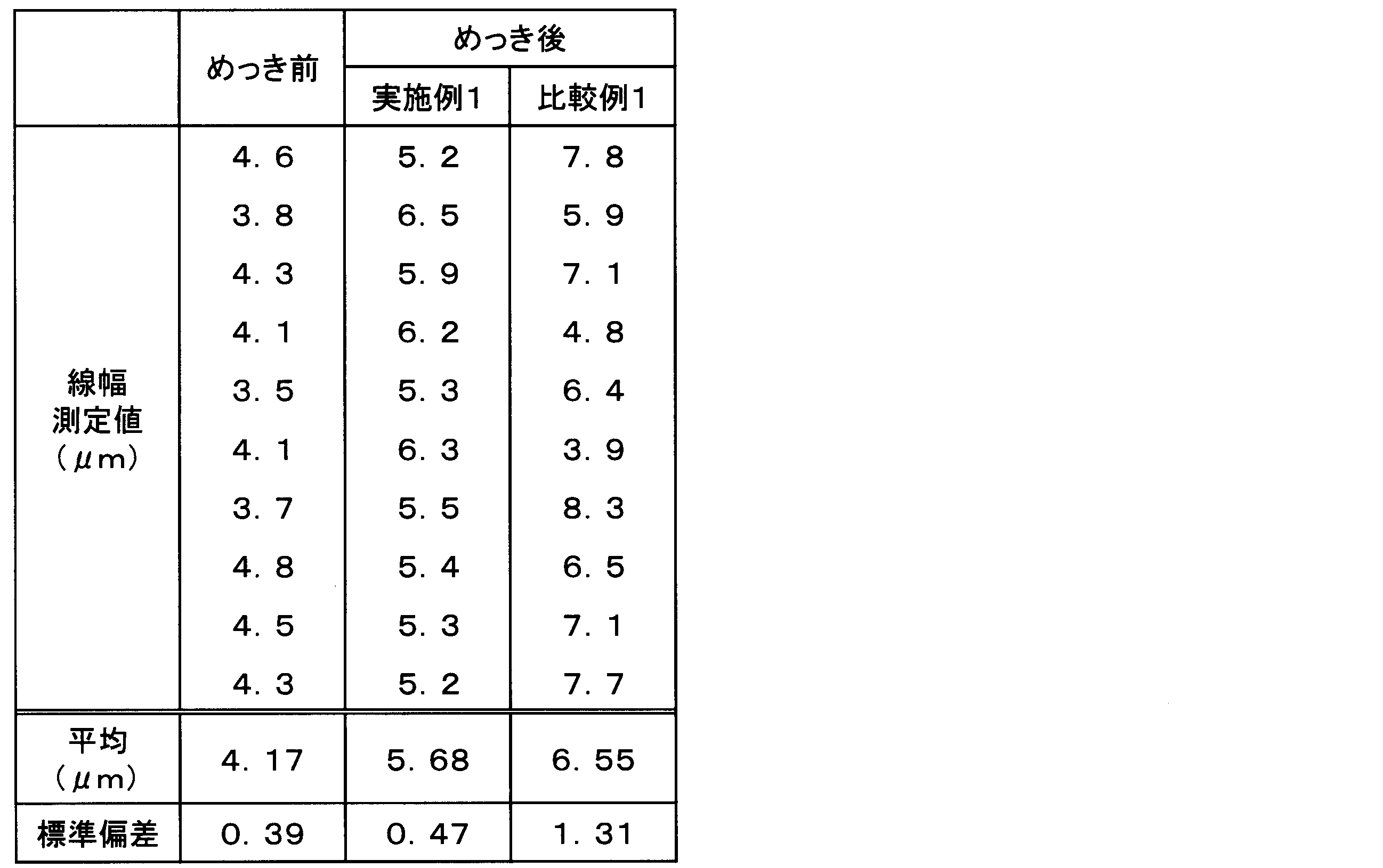
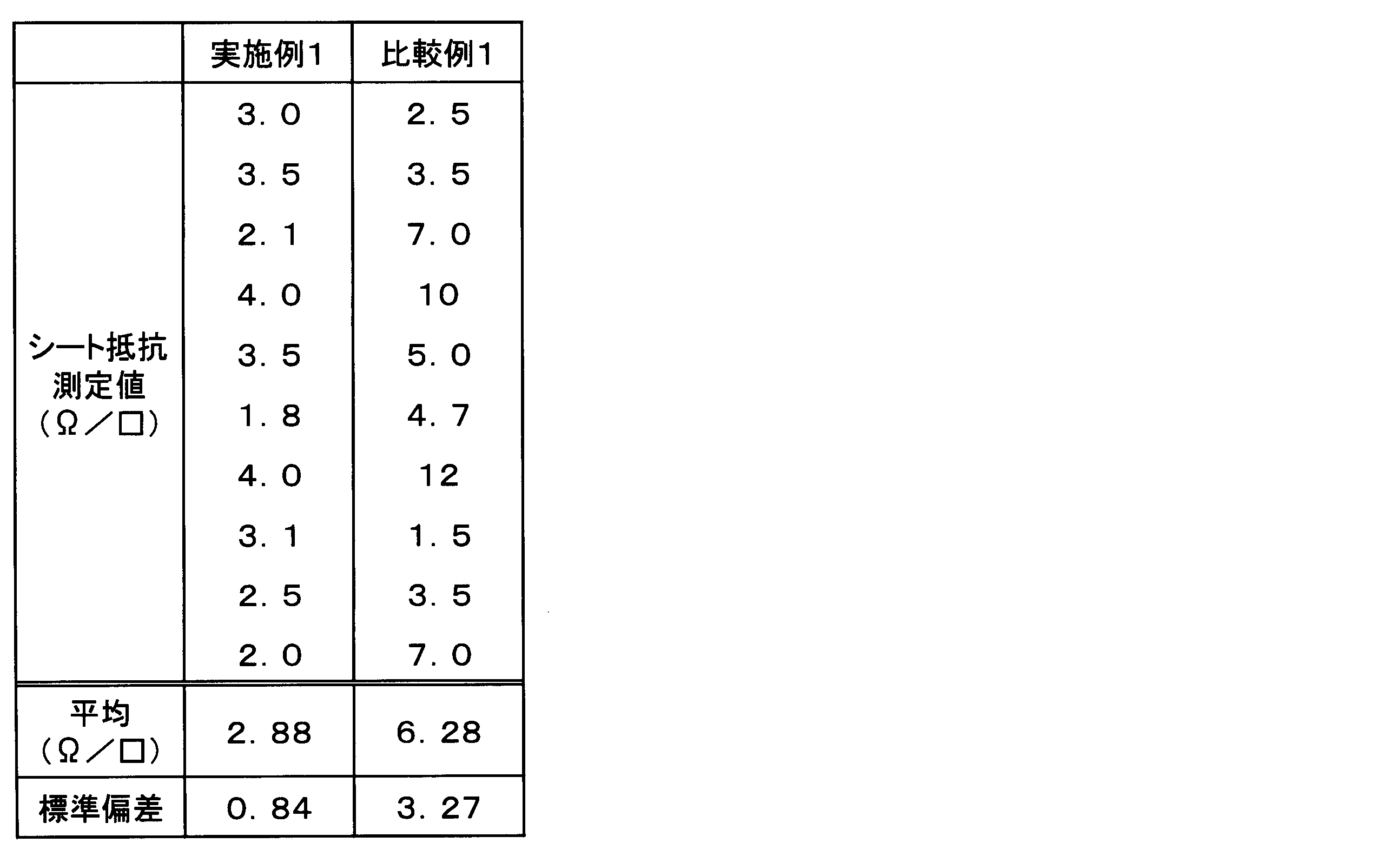
(実施例2)
図5に示したものと同様の長尺状のセンサー基材前駆体1’を作成した。センサーチャネル12を構成する複数の導電性細線13はインクジェット法により形成した。複数のセンサーチャネル12によって形成されるセンサーパターン部Sの大きさは60インチ(幅約1300mm、高さ約750mm)である。センサー基材前駆体1’の長手方向に沿って、センサーパターン部Sを5つ形成した。
図5に示したものと同様の長尺状のセンサー基材前駆体1’を作成した。センサーチャネル12を構成する複数の導電性細線13はインクジェット法により形成した。複数のセンサーチャネル12によって形成されるセンサーパターン部Sの大きさは60インチ(幅約1300mm、高さ約750mm)である。センサー基材前駆体1’の長手方向に沿って、センサーパターン部Sを5つ形成した。
次いで、図6に示したものと同様のめっき装置を用いて、センサー基材前駆体1’のめっき用バスライン5から、複数のめっき用引出配線14’を介して、複数のセンサーチャネル12に給電して、銅めっき浴中で電解めっき(銅めっき)を施した。
1つのセンサーパターン部Sについて、複数のセンサーチャネル12の中から無作為に選択した10箇所で、めっき前の導電性細線13の線幅を測定した。測定された値は、他の4つのセンサーパターン部Sにおいても略同じ値であった。また、5つのセンサーパターン部S(No.1~5)のそれぞれについて、複数のセンサーチャネル12の中から無作為に選択した10箇所で、めっき後の導電性細線13の線幅を測定した。更に、無作為に選択した10箇所で、めっき後のセンサーチャネル12のシート抵抗を測定した。これらの測定値、平均及び標準偏差を表3に示す。

(実施例3)
実施例1においてめっきが施されたセンサー基材前駆体1’を図4(a)に示した一点鎖線Cに沿って裁断し、図1に示したものと同様のセンサー基材1を得た。
実施例1においてめっきが施されたセンサー基材前駆体1’を図4(a)に示した一点鎖線Cに沿って裁断し、図1に示したものと同様のセンサー基材1を得た。
次いで、得られたセンサー基材1を、図1に示したものと同様の配線基材2と接続した。その際、センサー基材1のセンサーチャネル12から伸びる導体14と、配線基材2の配線22とを、導電部材4によって接続した。
導電部材4として金属ペースト(導電性ペースト)を塗布した場合、導電部材4として銅箔テープを貼付けた場合、及び導電部材4としてセンサーチャネルと同様の導電性のメッシュパターンを貼付けた場合の何れにおいても、センサーチャネル12と配線22とが安定に電気的に接続されることが確認された。
1:センサー基材
11:基材
12:センサーチャネル
13:導電性細線
14:導体
S:センサーパターン部
2:配線基材
21:基材
22:配線
23:スルーホール
24:帯状部
W:引出配線パターン部
3:外部接続部品の接続部位
4:導電部材
41:支持体
11:基材
12:センサーチャネル
13:導電性細線
14:導体
S:センサーパターン部
2:配線基材
21:基材
22:配線
23:スルーホール
24:帯状部
W:引出配線パターン部
3:外部接続部品の接続部位
4:導電部材
41:支持体
Claims (20)
- 複数のセンサーチャネルからなるセンサーパターン部を有する少なくとも1つのセンサー基材と、複数の配線からなる引出配線パターン部を有する少なくとも1つの配線基材とを用意し、
次いで、前記センサー基材の前記センサーチャネルと前記配線基材の前記配線とが電気的に接続されるように、前記センサー基材と前記配線基材とを接続するタッチパネルセンサー基材の製造方法。 - 前記複数のセンサーチャネルと前記複数の配線とが1対1に対応するように前記センサー基材と前記配線基材とを配置し、
次いで、前記センサー基材の前記センサーチャネルと前記配線基材の前記配線とを導電部材によって電気的に接続する請求項1記載のタッチパネルセンサー基材の製造方法。 - 前記センサー基材の前記センサーチャネル、及び、前記配線基材の前記配線から選ばれる少なくとも1つ以上を、めっき処理を施して製造する請求項1又は2記載のタッチパネルセンサー基材の製造方法。
- 前記めっき処理が電解めっきである請求項3記載のタッチパネルセンサー基材の製造方法。
- 複数のセンサーチャネルと、前記複数のセンサーチャネルに対して電気的に接続されためっき用バスラインとが形成されたセンサー基材前駆体を用意し、
次いで、前記めっき用バスラインを介して前記複数のセンサーチャネルに給電することによって、前記複数のセンサーチャネルに電解めっきを施し、
次いで、前記センサー基材前駆体のうち前記めっき用バスラインが設けられた領域を切除して、前記センサー基材を製造する請求項4記載のタッチパネルセンサー基材の製造方法。 - 前記センサー基材の前記センサーチャネル、及び、前記配線基材の前記配線から選ばれる少なくとも1つ以上を、インクジェット法により形成した後、めっき処理を施して製造する請求項3~5の何れかに記載のタッチパネルセンサー基材の製造方法。
- 前記センサー基材の前記センサーチャネルの製法と、前記配線基材の前記配線の製法とが異なる請求項1~6の何れかに記載のタッチパネルセンサー基材の製造方法。
- 前記配線基材の前記配線をレーザー処理により製造する請求項1~7の何れかに記載のタッチパネルセンサー基材の製造方法。
- 前記配線基材の前記配線をフォトリソグラフィー処理により製造する請求項1~7の何れかに記載のタッチパネルセンサー基材の製造方法。
- 前記配線基材の前記配線をスクリーン印刷処理により製造する請求項1~7の何れかに記載のタッチパネルセンサー基材の製造方法。
- 前記センサー基材の前記センサーチャネル、及び、前記配線基材の前記配線から選ばれる少なくとも1つ以上を、ロールtoロール処理により製造する請求項1~10の何れかに記載のタッチパネルセンサー基材の製造方法。
- 前記センサー基材は前記センサーパターン部を両面に有する請求項1~11の何れかに記載のタッチパネルセンサー基材の製造方法。
- 前記配線基材は該配線基材の一端部から帯状に延設された帯状部を備え、
前記帯状部には、前記複数の配線が、該帯状部の長手方向に沿って該帯状部の末端まで伸びている請求項1~12の何れかに記載のタッチパネルセンサー基材の製造方法。 - 前記配線基材を前記センサー基材に接続する前に、前記帯状部を形成するように前記配線基材を裁断する請求項13記載のタッチパネルセンサー基材の製造方法。
- タッチパネルセンサーを構成するための基材セットであって、
複数のセンサーチャネルからなるセンサーパターン部を有する少なくとも1つのセンサー基材と、
複数の配線からなる引出配線パターン部を有する少なくとも1つの配線基材と、によって構成されたタッチパネルセンサー基材セット。 - 前記センサー基材の前記センサーチャネルは複数の導電性細線によって構成され、
前記複数の導電性細線の平均線幅バラツキが標準偏差0.5以下である請求項15記載のタッチパネルセンサー基材セット。 - 前記センサー基材の同一面上に設けられた前記複数のセンサーチャネルの平均抵抗バラツキが標準偏差1以下である請求項15又は16記載のタッチパネルセンサー基材セット。
- 前記センサー基材の前記センサーチャネルはめっき皮膜を有する請求項15~17の何れかに記載のタッチパネルセンサー基材セット。
- 前記センサー基材の前記センサーチャネルと前記配線基材の前記配線とが導電部材によって電気的に接続されている請求項15~18の何れかに記載のタッチパネルセンサー基材セット。
- 前記センサー基材は前記センサーパターン部を両面に有する請求項15~19の何れかに記載のタッチパネルセンサー基材セット。
Priority Applications (2)
| Application Number | Priority Date | Filing Date | Title |
|---|---|---|---|
| JP2019568530A JPWO2019150563A1 (ja) | 2018-02-02 | 2018-02-02 | タッチパネルセンサー基材の製造方法及びタッチパネルセンサー基材セット |
| PCT/JP2018/003687 WO2019150563A1 (ja) | 2018-02-02 | 2018-02-02 | タッチパネルセンサー基材の製造方法及びタッチパネルセンサー基材セット |
Applications Claiming Priority (1)
| Application Number | Priority Date | Filing Date | Title |
|---|---|---|---|
| PCT/JP2018/003687 WO2019150563A1 (ja) | 2018-02-02 | 2018-02-02 | タッチパネルセンサー基材の製造方法及びタッチパネルセンサー基材セット |
Publications (1)
| Publication Number | Publication Date |
|---|---|
| WO2019150563A1 true WO2019150563A1 (ja) | 2019-08-08 |
Family
ID=67479289
Family Applications (1)
| Application Number | Title | Priority Date | Filing Date |
|---|---|---|---|
| PCT/JP2018/003687 Ceased WO2019150563A1 (ja) | 2018-02-02 | 2018-02-02 | タッチパネルセンサー基材の製造方法及びタッチパネルセンサー基材セット |
Country Status (2)
| Country | Link |
|---|---|
| JP (1) | JPWO2019150563A1 (ja) |
| WO (1) | WO2019150563A1 (ja) |
Cited By (2)
| Publication number | Priority date | Publication date | Assignee | Title |
|---|---|---|---|---|
| JP2021060891A (ja) * | 2019-10-09 | 2021-04-15 | パナソニックIpマネジメント株式会社 | タッチセンサ中間体およびその製造方法、ならびにタッチセンサ中間体の検査方法 |
| CN113168262A (zh) * | 2018-12-19 | 2021-07-23 | 日写株式会社 | 触控面板、触控面板模块和触控面板的检测方法 |
Citations (3)
| Publication number | Priority date | Publication date | Assignee | Title |
|---|---|---|---|---|
| WO2014171103A1 (ja) * | 2013-04-18 | 2014-10-23 | シャープ株式会社 | タッチパネルモジュール及び電子情報機器 |
| WO2014171102A1 (ja) * | 2013-04-18 | 2014-10-23 | シャープ株式会社 | センサシート、センサシートモジュール、タッチセンサパネルモジュールおよび電子機器 |
| WO2016158085A1 (ja) * | 2015-03-27 | 2016-10-06 | 富士フイルム株式会社 | タッチセンサーおよびタッチパネル |
-
2018
- 2018-02-02 WO PCT/JP2018/003687 patent/WO2019150563A1/ja not_active Ceased
- 2018-02-02 JP JP2019568530A patent/JPWO2019150563A1/ja active Pending
Patent Citations (3)
| Publication number | Priority date | Publication date | Assignee | Title |
|---|---|---|---|---|
| WO2014171103A1 (ja) * | 2013-04-18 | 2014-10-23 | シャープ株式会社 | タッチパネルモジュール及び電子情報機器 |
| WO2014171102A1 (ja) * | 2013-04-18 | 2014-10-23 | シャープ株式会社 | センサシート、センサシートモジュール、タッチセンサパネルモジュールおよび電子機器 |
| WO2016158085A1 (ja) * | 2015-03-27 | 2016-10-06 | 富士フイルム株式会社 | タッチセンサーおよびタッチパネル |
Cited By (2)
| Publication number | Priority date | Publication date | Assignee | Title |
|---|---|---|---|---|
| CN113168262A (zh) * | 2018-12-19 | 2021-07-23 | 日写株式会社 | 触控面板、触控面板模块和触控面板的检测方法 |
| JP2021060891A (ja) * | 2019-10-09 | 2021-04-15 | パナソニックIpマネジメント株式会社 | タッチセンサ中間体およびその製造方法、ならびにタッチセンサ中間体の検査方法 |
Also Published As
| Publication number | Publication date |
|---|---|
| JPWO2019150563A1 (ja) | 2021-01-28 |
Similar Documents
| Publication | Publication Date | Title |
|---|---|---|
| JP4968414B2 (ja) | 透明導電層付き基体及びその製造方法、並びにタッチパネル用透明導電膜積層体、タッチパネル | |
| TWI551537B (zh) | 導電膜及含有該導電膜的觸控面板 | |
| KR102170097B1 (ko) | 도전성 기판 및 도전성 기판 제조방법 | |
| CN104635983A (zh) | 触摸开关 | |
| US8772645B2 (en) | Touch panel and display device including same | |
| WO2019150563A1 (ja) | タッチパネルセンサー基材の製造方法及びタッチパネルセンサー基材セット | |
| JP5757800B2 (ja) | タッチパネル | |
| JP6439641B2 (ja) | 導電性パターンの形成方法及び導電性パターン | |
| CN106470530B (zh) | 功能性细线图案、带透明导电膜的基材及其制造方法 | |
| JP6081187B2 (ja) | 配線基板、タッチパネルセンサシートおよび太陽電池用電極基板 | |
| CN102081486A (zh) | 一种电容式触摸感应器 | |
| WO2019150562A1 (ja) | タッチパネルセンサーの製造方法及びタッチパネルセンサー基材セット | |
| JP7119619B2 (ja) | タッチパネルセンサー前駆体及びタッチパネルセンサーの製造方法 | |
| WO2020129506A1 (ja) | タッチパネル、タッチパネルモジュールおよびタッチパネルの検査方法 | |
| WO2019064595A1 (ja) | タッチパネルセンサー及びタッチパネルセンサーの製造方法 | |
| JP2017118069A (ja) | 電解メッキ方法 | |
| JP2018098446A (ja) | タッチパネルセンサー中間体、及びタッチパネルセンサーの製造方法 | |
| TW201710564A (zh) | 黑化鍍液、導電性基板 | |
| WO2019215929A1 (ja) | タッチセンサーフィルムの製造方法及びタッチセンサーフィルム中間体 | |
| JP5558511B2 (ja) | 導電性ナノファイバーシート及びこれを用いたタッチパネル | |
| CN105517333A (zh) | 柔性电路板及终端 | |
| CN111727669B (zh) | 图案形成方法 | |
| JP2012156031A (ja) | 導電性フィルム | |
| JP2019020983A (ja) | センサーフィルムの製造方法及びセンサーフィルム | |
| WO2017110580A1 (ja) | 機能性細線パターン及び機能性細線パターンの製造方法 |
Legal Events
| Date | Code | Title | Description |
|---|---|---|---|
| 121 | Ep: the epo has been informed by wipo that ep was designated in this application |
Ref document number: 18903691 Country of ref document: EP Kind code of ref document: A1 |
|
| ENP | Entry into the national phase |
Ref document number: 2019568530 Country of ref document: JP Kind code of ref document: A |
|
| NENP | Non-entry into the national phase |
Ref country code: DE |
|
| 122 | Ep: pct application non-entry in european phase |
Ref document number: 18903691 Country of ref document: EP Kind code of ref document: A1 |