WO2019144303A1 - Capacitance detection circuit, touch apparatus, and terminal device - Google Patents
Capacitance detection circuit, touch apparatus, and terminal device Download PDFInfo
- Publication number
- WO2019144303A1 WO2019144303A1 PCT/CN2018/073907 CN2018073907W WO2019144303A1 WO 2019144303 A1 WO2019144303 A1 WO 2019144303A1 CN 2018073907 W CN2018073907 W CN 2018073907W WO 2019144303 A1 WO2019144303 A1 WO 2019144303A1
- Authority
- WO
- WIPO (PCT)
- Prior art keywords
- switch
- capacitor
- phase
- charge
- capacitance
- Prior art date
Links
Images


Classifications
-
- G—PHYSICS
- G01—MEASURING; TESTING
- G01R—MEASURING ELECTRIC VARIABLES; MEASURING MAGNETIC VARIABLES
- G01R27/00—Arrangements for measuring resistance, reactance, impedance, or electric characteristics derived therefrom
- G01R27/02—Measuring real or complex resistance, reactance, impedance, or other two-pole characteristics derived therefrom, e.g. time constant
- G01R27/26—Measuring inductance or capacitance; Measuring quality factor, e.g. by using the resonance method; Measuring loss factor; Measuring dielectric constants ; Measuring impedance or related variables
- G01R27/2605—Measuring capacitance
-
- G—PHYSICS
- G01—MEASURING; TESTING
- G01R—MEASURING ELECTRIC VARIABLES; MEASURING MAGNETIC VARIABLES
- G01R35/00—Testing or calibrating of apparatus covered by the other groups of this subclass
- G01R35/005—Calibrating; Standards or reference devices, e.g. voltage or resistance standards, "golden" references
-
- G—PHYSICS
- G06—COMPUTING; CALCULATING OR COUNTING
- G06F—ELECTRIC DIGITAL DATA PROCESSING
- G06F3/00—Input arrangements for transferring data to be processed into a form capable of being handled by the computer; Output arrangements for transferring data from processing unit to output unit, e.g. interface arrangements
- G06F3/01—Input arrangements or combined input and output arrangements for interaction between user and computer
- G06F3/03—Arrangements for converting the position or the displacement of a member into a coded form
- G06F3/041—Digitisers, e.g. for touch screens or touch pads, characterised by the transducing means
- G06F3/0416—Control or interface arrangements specially adapted for digitisers
-
- G—PHYSICS
- G06—COMPUTING; CALCULATING OR COUNTING
- G06F—ELECTRIC DIGITAL DATA PROCESSING
- G06F3/00—Input arrangements for transferring data to be processed into a form capable of being handled by the computer; Output arrangements for transferring data from processing unit to output unit, e.g. interface arrangements
- G06F3/01—Input arrangements or combined input and output arrangements for interaction between user and computer
- G06F3/03—Arrangements for converting the position or the displacement of a member into a coded form
- G06F3/041—Digitisers, e.g. for touch screens or touch pads, characterised by the transducing means
- G06F3/044—Digitisers, e.g. for touch screens or touch pads, characterised by the transducing means by capacitive means
-
- H—ELECTRICITY
- H03—ELECTRONIC CIRCUITRY
- H03K—PULSE TECHNIQUE
- H03K17/00—Electronic switching or gating, i.e. not by contact-making and –breaking
- H03K17/94—Electronic switching or gating, i.e. not by contact-making and –breaking characterised by the way in which the control signals are generated
- H03K17/96—Touch switches
- H03K17/962—Capacitive touch switches
-
- H—ELECTRICITY
- H03—ELECTRONIC CIRCUITRY
- H03K—PULSE TECHNIQUE
- H03K2217/00—Indexing scheme related to electronic switching or gating, i.e. not by contact-making or -breaking covered by H03K17/00
- H03K2217/94—Indexing scheme related to electronic switching or gating, i.e. not by contact-making or -breaking covered by H03K17/00 characterised by the way in which the control signal is generated
- H03K2217/96—Touch switches
- H03K2217/9607—Capacitive touch switches
- H03K2217/960735—Capacitive touch switches characterised by circuit details
- H03K2217/96074—Switched capacitor
Definitions
- Embodiments of the present application relate to the field of capacitance detection, and more particularly, to a capacitance detection circuit, a touch device, and a terminal device.
- Capacitive sensors are widely used in electronic devices.
- the capacitive sensor can be used as an input device to provide input information such as position, motion, force, and duration.
- the core part of the capacitive sensor is a capacitance detecting circuit.
- the capacitance detecting circuit includes a sensor capacitor, an integrator and an analog to digital converter (ADC).
- ADC analog to digital converter
- the capacitance value of the sensor capacitor changes, and the integrator uses The capacitive effect generated when the user operates the capacitive sensor is converted into a voltage signal, which is sampled by the ADC and converted into a digital signal, and then the capacitance detection can be performed according to the digital signal.
- a calibration capacitor may be added to the capacitance detecting circuit, and the capacitance value of the calibration capacitor is generally set to be approximately equal to the capacitance value of the sensor capacitor when the capacitive sensor is not operated. Therefore, if the capacitance value of the sensor capacitor is large when the capacitive sensor is not operated, the capacitance value of the calibration capacitor is also large, which increases the area of the capacitance detecting circuit and increases the cost of the chip.
- the embodiment of the present application provides a capacitance detecting circuit, a touch device, and a terminal device, which are beneficial for reducing the area of the capacitance detecting circuit, thereby reducing the cost of the chip.
- a capacitance detecting circuit is provided that is coupled to a detecting capacitor, the capacitance detecting circuit comprising:
- a charge and discharge module comprising a first current source for charging or discharging the detection capacitor, and a second current source for charging or discharging the calibration capacitor ;
- control module configured to control an operating state of the charging and discharging module and the integrator.
- the detecting capacitor and the calibration capacitor can be respectively charged or discharged by the first current source and the second current source, so that the first current can be adjusted.
- the proportional relationship between the current values of the source and the second current source reaches the purpose of adjusting the capacitance value of the calibration capacitor. For example, by setting the current value of the first current source to be greater than the current value of the second current source, the capacitance value of the calibration capacitor can be realized. It is smaller than the reference capacitance value, so that the area of the capacitance detecting circuit can be reduced, and the cost of the chip can be reduced.
- the calibration capacitor is configured to make an output voltage of the integrator a reference voltage when a capacitance value of the detection capacitor is a reference capacitance value, wherein the reference capacitance value and a capacitance value of the calibration capacitor
- the ratio is equal to the ratio of the current value of the first current source to the current value of the second current source.
- the capacitance detecting circuit further includes a charging and discharging switch group, a clearing switch group, and an integrating switch group, and the integrator includes an integrating capacitor and an amplifier;
- the control module is specifically configured to:
- the first current source and the second current source Controlling, by the charge and discharge switch group, the first current source and the second current source to respectively charge or discharge the detection capacitor and the calibration capacitor during a charge and discharge phase, wherein in the charge and discharge phase And a voltage on the detecting capacitor is charged to the reference voltage or discharged to the reference voltage, a charging duration of the calibration capacitor is equal to a charging duration of the detecting capacitor, or a discharge duration of the calibration capacitor is
- the detection capacitors have the same discharge duration;
- a portion of the charge stored on the calibration capacitor is controlled to be transferred to the integrating capacitor by the integrating switch group.
- the charge and discharge switch group includes a first switch, a second switch, a third switch, and a fourth switch
- the integral switch group includes a fifth switch
- the clear switch group includes a sixth switch
- One end of the first switch is connected to one end of the first current source, the other end of the first current source is connected to a power supply voltage, and the other end of the first switch is connected to one end of the detecting capacitor and the third One end of the switch, the other end of the detecting capacitor and the other end of the third switch are grounded;
- One end of the second switch is connected to one end of the second current source, the other end of the second current source is connected to a power supply voltage, and the other end of the second switch is connected to one end of the calibration capacitor and the fourth One end of the switch, the other end of the calibration capacitor and the other end of the fourth switch are grounded;
- One end of the fifth switch is connected to one end of the calibration capacitor, the other end of the fifth switch is connected to the first input end of the amplifier, and the second input end of the amplifier is used for inputting the reference voltage;
- the sixth switch is connected in parallel with the integrating capacitor, and the integrating capacitor is connected in parallel with the amplifier.
- the sixth switch in the charge clearing phase, is closed, the first switch, the second switch, the third switch, the fourth switch, and the first The five switches are all turned off, and the charge stored on the integrating capacitor is cleared;
- the charge and discharge phase includes a discharge phase and a charge phase, the discharge phase being prior to the charging phase, wherein:
- the third switch and the fourth switch are closed, the first switch, the second switch, the fifth switch and the sixth switch are both turned off, and the detecting capacitor is cleared And a charge stored on the calibration capacitor;
- the first switch and the second switch are closed, the third switch, the fourth switch, the fifth switch and the sixth switch are turned off, and the voltage on the detecting capacitor Charged to the reference voltage, after the voltage on the detection capacitor is charged to the reference voltage, the first switch and the second switch are turned off;
- the first switch, the second switch, the third switch, the fourth switch, and the sixth switch are both turned off, the fifth switch is closed, and the calibration A portion of the charge on the capacitor is transferred to the integrating capacitor.
- a first buffer phase is further included between the charge and discharge phase and the charge transfer phase, and a second buffer phase is further included after the charge transfer phase, the first buffer phase and The second buffering stage is for maintaining a constant charge on the detecting capacitor, the calibration capacitor, and the integrating capacitor;
- the first switch, the second switch, the third switch, the fourth switch, the fifth switch, and the first The six switches are all disconnected.
- the capacitance detecting circuit of the embodiment of the present application can discharge the detecting capacitor and the calibration capacitor by the first current source and the second current source respectively by discharging the detecting capacitor and the calibration capacitor, thereby achieving the first current passing through
- the proportional relationship between the current values of the source and the second current source controls the proportional relationship between the reference capacitance value and the capacitance value of the calibration capacitor, and therefore, the current value of the first current source is set to be greater than the second current source
- the current value can achieve the purpose of reducing the capacitance value of the calibration capacitor, thereby reducing the area of the capacitance detection circuit and reducing the cost of the chip.
- control module is further configured to:
- Controlling the charge and discharge switch group, the integral switch group, and the clear switch group repeatedly performs operations from the charge and discharge phase to the second buffer phase.
- the output voltage V out of the integrator is:
- the V R is the reference voltage
- the ⁇ C x is a change amount of the detection capacitor relative to the reference capacitance value
- the C S is a capacitance value of the integration capacitor
- the I 1 is a current value of the first current source
- the I 2 is a current value of the second current source
- the N is a number of executions of the charging and discharging phase to the second buffering phase.
- the capacitance detecting circuit of the embodiment of the present application facilitates the improvement of the sensitivity of the capacitance detection by performing the operation from the charging and discharging stage to the second buffering stage a plurality of times.
- the charge and discharge switch group includes a first switch, a second switch, a third switch, and a fourth switch
- the integral switch group includes a fifth switch
- the clear switch group includes a sixth switch
- One end of the first switch is connected to one end of the first current source, the other end of the first current source is grounded, and the other end of the first switch is connected to one end of the detecting capacitor and the third switch One end, the other end of the detecting capacitor is grounded, and the other end of the third switch is connected to a power supply voltage;
- One end of the second switch is connected to one end of the second current source, the other end of the second current source is grounded, and the other end of the second switch is connected to one end of the calibration capacitor and the fourth switch One end, the other end of the calibration capacitor is grounded, and the other end of the fourth switch is connected to a power supply voltage;
- One end of the fifth switch is connected to one end of the calibration capacitor, the other end of the fifth switch is connected to the first input end of the amplifier, and the second input end of the amplifier is used for inputting the reference voltage;
- the sixth switch is connected in parallel with the integrating capacitor, and the integrating capacitor is connected in parallel with the amplifier.
- the sixth switch in the charge clearing phase, is closed, the first switch, the second switch, the third switch, the fourth switch, and the first The five switches are all turned off, and the charge stored on the integrating capacitor is cleared;
- the charge and discharge phase includes a charge phase and a discharge phase, the charge phase being prior to the discharge phase, wherein:
- the third switch and the fourth switch are closed, the first switch, the second switch, the fifth switch, and the sixth switch are both turned off, the detecting capacitor and the The voltage on the calibration capacitor is charged to the supply voltage;
- the first switch and the second switch are closed, and the third switch, the fourth switch, the fifth switch, and the sixth switch are both turned off, on the detecting capacitor a voltage is discharged from the power supply voltage to the reference voltage, and after the voltage on the detection capacitor is discharged to the reference voltage, the first switch and the second switch are turned off;
- the first switch, the second switch, the third switch, the fourth switch, and the sixth switch are both turned off, the fifth switch is closed, and the calibration A portion of the charge on the capacitor is transferred to the integrating capacitor.
- a first buffer phase is further included between the charge and discharge phase and the charge transfer phase, and a second buffer phase is further included after the charge transfer phase, the first buffer phase and The second buffering stage is for maintaining a constant charge on the detecting capacitor, the calibration capacitor, and the integrating capacitor;
- the first switch, the second switch, the third switch, the fourth switch, the fifth switch, and the first The six switches are all disconnected.
- the capacitance detecting circuit of the embodiment of the present application can charge the detecting capacitor and the calibration capacitor by first discharging the detecting capacitor and the calibration capacitor, respectively, thereby discharging the first current through the first current source and the second current source.
- the proportional relationship between the current values of the source and the second current source controls the proportional relationship between the reference capacitance value and the capacitance value of the calibration capacitor, and therefore, the current value of the first current source is set to be greater than the second current source
- the current value can achieve the purpose of reducing the capacitance value of the calibration capacitor, thereby reducing the area of the capacitance detection circuit and reducing the cost of the chip.
- control module is further configured to:
- Controlling the charge and discharge switch group, the integral switch group, and the clear switch group repeatedly performs operations from the charge and discharge phase to the second buffer phase.
- the output voltage V out of the integrator is:
- V R is the reference voltage
- the ⁇ C x is a change amount of a capacitance value of the detection capacitor with respect to the reference capacitance value
- the C S is a capacitance value of the integration capacitor
- the I 1 a current value of the first current source
- the I 2 is a current value of the second current source
- the V DD is the power supply voltage
- the N is the charging and discharging phase to the second The number of executions of the buffer phase.
- the capacitance detecting circuit of the embodiment of the present application is advantageous for improving the sensitivity of the capacitance detection by performing the operation of the charging and discharging phase to the second buffering phase a plurality of times.
- the capacitance detecting circuit further includes a comparator, a first input end of the comparator is connected to the detecting capacitor, and a second input end of the comparator is used to input the reference voltage, The output of the comparator is connected to the control module;
- the output signal of the comparator is inverted when the voltage of the detecting capacitor reaches the reference voltage, and the control module controls the charging and discharging module to stop charging or discharging the detecting capacitor and the calibration capacitor.
- the capacitance detecting circuit further includes a processing module, configured to determine, according to an output voltage of the integrator, an amount of change in a capacitance value of the detecting capacitor relative to the reference capacitance value.
- the current value of the first current source is greater than the current value of the second current source.
- the capacitance detecting circuit is applied to a capacitive sensor, the detecting capacitor is a sensor capacitance of the capacitive sensor, and the reference capacitance value is the sensor capacitance when the capacitive sensor is not operated. Capacitance value.
- a touch device comprising the capacitance detecting circuit of the first aspect and any possible implementation of the first aspect.
- a terminal device comprising the capacitance detecting circuit of the first aspect and any one of the possible implementations of the first aspect.
- FIG. 1 is a schematic structural diagram of a capacitance detecting circuit according to an embodiment of the present application.
- FIG. 2 is a schematic diagram of a capacitance detecting circuit in accordance with an embodiment of the present application.
- FIG. 3 is a logic timing diagram of a capacitance detecting circuit in accordance with an embodiment of the present application.
- FIG. 4 is a schematic diagram of a capacitance detecting circuit according to another embodiment of the present application.
- FIG. 5 is a logic timing diagram of a capacitance detecting circuit according to another embodiment of the present application.
- FIG. 6 is a schematic structural diagram of a touch device according to an embodiment of the present application.
- FIG. 7 is a schematic structural diagram of a terminal device according to an embodiment of the present application.
- FIG. 1 is a schematic structural diagram of a capacitance detecting circuit 100 according to an embodiment of the present application. As shown in FIG. 1, the capacitance detecting circuit 100 is connected to a detecting capacitor 110, and the capacitor detecting circuit 100 includes:
- the charge and discharge module 130 includes a first current source 141 for charging or discharging the detection capacitor 110, and a second current source 142 for Calibrating the capacitor 120 for charging or discharging;
- An integrator 150 configured to convert a capacitance signal of the detection capacitor 130 into a voltage signal
- the control module 130 is configured to control an operating state of the charging and discharging module 140 and the integrator 150.
- the calibration capacitor 120 is configured to make an output voltage of the integrator 150 a reference voltage when a capacitance value of the detection capacitor 110 is a reference capacitance value, where the reference A ratio of the capacitance value to the capacitance value of the calibration capacitor is equal to a ratio of a current value of the first current source 141 to a current value of the second current source 142.
- the capacitance detecting circuit of the embodiment of the present application can be applied to various circuits or systems that need to perform capacitance detection.
- the capacitance detecting circuit can be applied to a capacitive sensor.
- the detecting capacitor can be a capacitor.
- the sensor capacitance of the sensor, the reference capacitance value of the detection capacitor may be a capacitance value of the sensor capacitance when the user does not operate the capacitance sensor, and the reference capacitance value may also be referred to as a basic capacitance, or a self-capacitance, etc., when the user operates the capacitance sensor,
- the capacitance value of the detection capacitor changes.
- the integrator can convert the capacitance signal (or voltage effect) of the detection capacitor into a voltage signal. Further, the capacitance value of the detection capacitor can be determined according to the voltage signal.
- the capacitance detecting circuit of the embodiment of the present application may include a first current source and a second current source, wherein the first current source and the second current source are respectively used to charge or discharge the detecting capacitor and the calibration capacitor .
- the calibration capacitor is configured to make an output voltage of the integrator a reference voltage when a capacitance value of the detection capacitor is a reference capacitance value, or the calibration capacitor is used to cancel the detection capacitor as a reference capacitor The amount of contribution to the output voltage of the integrator.
- the purpose of adjusting the capacitance value of the calibration capacitor can be achieved by adjusting a proportional relationship between a current value of the first current source and a current value of the second current source, for example, Setting a current value of the first current source to be greater than a current value of the second current source, so that a capacitance value of the calibration capacitor can be made smaller than a reference capacitance value of the detection capacitor, relative to the prior art adoption and detection
- the calibration capacitors with equal or approximately equal reference capacitance values of the capacitors are advantageous for reducing the area of the capacitance detecting circuit and reducing the cost of the chip.
- the calibration capacitor may be a capacitor or a capacitor array with a variable capacitance value, or may be a capacitor or a capacitor array with a fixed capacitance value, which is not limited in this embodiment of the present application.
- the first current source and the second current source may be current sources having a proportional relationship, for example, the first current source and the second current source may be obtained by mirroring a current source, the first The proportional relationship between the current value of the current source and the current value of the second current source may be fixed or adjustable, which is not limited in the embodiment of the present application.
- the capacitance detecting circuit 100 may further include a charging and discharging switch group, a clearing switch group, and an integrating switch group, and the integrator may include an integrating capacitor and an amplifier;
- the control module 130 can control the working states of the charging and discharging module and the integrator through the charging and discharging switch group, the clearing switch group and the integral switch group, for example, when the charging and discharging module is controlled
- the detection capacitor and the calibration capacitor are charged, and when the detection capacitor and the calibration capacitor are discharged, and when the integrator is controlled to integrate or the like.
- the charge stored on the integrating capacitor is cleared by the clear switch group
- the first current source and the second current source Controlling, by the charge and discharge switch group, the first current source and the second current source to respectively charge or discharge the detection capacitor and the calibration capacitor during a charge and discharge phase, wherein in the charge and discharge phase And a voltage on the detecting capacitor is charged to the reference voltage or discharged to the reference voltage, a charging duration of the calibration capacitor is equal to a charging duration of the detecting capacitor, or a discharge duration of the calibration capacitor is
- the detection capacitors have the same discharge duration;
- a portion of the charge stored on the calibration capacitor is controlled to be transferred to the integrating capacitor by the integrating switch group.
- a first buffering phase may be further included between the charging and discharging phase and the charge transfer phase
- a second buffering phase may be further included after the charging and transferring phase, a first buffering phase and a second buffering phase for avoiding charge leakage problems caused by frequent switching of switches, wherein in the first buffering phase and the second buffering phase, the detecting capacitor, the calibration The charge on the capacitor and the integrating capacitor does not change.
- the capacitance detecting circuit 100 may further include a comparator, a first input of the comparator is connected to the detecting capacitor, and a second input of the comparator is used for inputting a reference voltage, the output of the comparator is connected to the control module;
- the control module controls the charge and discharge module to stop charging or discharging the detection capacitor and the calibration capacitor when an output signal of the comparator is inverted.
- the control module can control the charging and discharging module to stop when the output signal of the comparator is inverted.
- the detecting capacitor and the calibration capacitor are charged or discharged, that is, controlling the first current source to stop charging or discharging the detecting capacitor, and controlling the second current source to stop charging or discharging the calibration capacitor .
- the control module may control, by the charging and discharging switch set, the charging and discharging module to stop charging or discharging the detecting capacitor and the calibration capacitor.
- the equivalent circuit of the comparator may also be used to implement the foregoing function, as long as the charging and discharging module stops the detecting capacitor and the device when the voltage of the detecting capacitor reaches the reference voltage.
- the calibration capacitor is charged or discharged, which is not specifically limited in the embodiment of the present application.
- the capacitance detecting circuit 100 further includes a processing module, configured to determine, according to an output voltage of the integrator, an amount of change in a capacitance value of the detecting capacitor with respect to the reference capacitance value.
- the processing module may be an ADC, or may be another circuit or module having a processing function, which is not limited in this embodiment of the present application.
- the processing module may determine a capacitance value of the detection capacitor according to an output voltage of the integrator. Specifically, the processing module may convert the voltage signal of the output of the integrator into a digital signal, and determine a capacitance value of the detecting capacitor according to the digital signal. For example, if the capacitance detecting circuit is applied in the capacitive sensor, the processing module may When the user does not operate the capacitive sensor, a digital signal is determined. When the user operates the capacitive sensor, another digital signal is determined, and then the amount of change in the capacitance of the sensor capacitance can be determined based on the difference between the two digital signals.
- FIG. 2 to FIG. 5 are intended to help those skilled in the art to better understand the embodiments of the present application, and do not limit the scope of the embodiments of the present application. It will be obvious to those skilled in the art that various modifications and changes can be made without departing from the scope of the embodiments of the present application.
- the capacitance detecting circuit 200 includes a detecting capacitor 210, a calibration capacitor 220, a control module 230, a charge and discharge module 240, an integrator 250, a processing module 260, and a comparator 270.
- the charging and discharging module 240 includes a first current source 241 and a second current source 242, and the integrator 250 includes an integrating capacitor 251 and an amplifier 252.
- the capacitance detecting circuit further includes a charging and discharging switch group, a clearing switch group and an integrating switch group, wherein the charging and discharging switch group includes a first switch 231, a second switch 232, a third switch 233, and a fourth switch 234,
- the integral switch group includes a fifth switch 235, and the clear switch group includes a sixth switch 236.
- one end of the first switch 231 is connected to one end of the first current source 241, and the other end of the first current source 241 is connected to a power supply voltage (ie, V DD ), and the other end of the first switch 231 is One end of the detecting capacitor 210 and one end of the third switch 233 are connected, and the other end of the detecting capacitor 210 and the other end of the third switch 233 are grounded, wherein the detecting capacitor 210 is a touch panel ( Touch panel) a measurement capacitor formed by the upper driving electrode and the sensing electrode;
- Touch panel Touch panel
- One end of the second switch 232 is connected to one end of the second current source 242, the other end of the second current source is connected to a power supply voltage (ie, V DD ), and the other end of the second switch 232 is connected to the calibration.
- One end of the capacitor 220 and one end of the fourth switch 234, the other end of the calibration capacitor 220 and the other end of the fourth switch 234 are grounded, that is, one end of the calibration capacitor 220 (for example, an upper plate)
- the second switch 232 and the second current source 242 are connected to the power supply voltage V DD , and the same end of the calibration capacitor 220 (such as the upper plate) is grounded through the fourth switch 234, and the calibration capacitor 220 is further One end (for example, the lower plate) is grounded.
- One end of the fifth switch 235 is connected to one end of the calibration capacitor 220, and the other end of the fifth switch 235 is connected to a first input end (ie, a negative input end) of the amplifier 252, and the second end of the amplifier 252
- the input terminal ie, the positive input terminal
- V R the reference voltage
- the sixth switch 236 is connected in parallel with the integrating capacitor 251, and the integrating capacitor 251 is connected in parallel with the amplifier 252, that is, the integrating capacitor 251 is connected across the negative input terminal and the output terminal of the amplifier 252;
- a first input terminal (eg, a positive input terminal) of the comparator 270 is coupled to one end of the detection capacitor 210, and a second input terminal (eg, a negative input terminal) of the comparator 270 is configured to input the reference voltage V R .
- a connection mode of the positive and negative input terminals of the comparator 270 can also be reversed, and the present invention does not limit this.
- the output of the integrator 250 can also be connected to the processing module 260.
- the processing module 260 can be used to process the output signal V out of the integrator 250 to determine the capacitance value of the detection capacitor 210.
- S1 to S6 are control signals of the first switch 231 to the sixth switch 236, respectively.
- the control signal is at a high level, the corresponding switch is closed, and when the control signal is low, the corresponding off switch, V x and V c are the detection voltage curve and the calibration capacitor 210 capacitor 220, V out is the output voltage of the integrator 250.
- the charge and discharge phase includes a discharge phase (corresponding to time periods t 1 to t 2 in FIG. 3 ) and a charging phase (corresponding to time periods t 2 to t 3 in FIG. 3 ).
- the discharge phase is before the charging phase.
- the detection capacitor 210 and the calibration capacitor 220 are first discharged, and then the detection capacitor 210 and the calibration capacitor 220 are charged.
- the third switch 233 and the fourth switch 234 are closed, the first switch 231, the second switch 232, the fifth switch 235, and the first The six switches 236 are both turned off, and the charge stored on the detecting capacitor 210 and the calibration capacitor 220 is cleared, that is, in the period t 1 to t 2 , the detecting capacitor 210 and the calibration capacitor 220 are completely discharged, at t At time 2 , the amount of charge on the detection capacitor 210 and the calibration capacitor 220 is zero, and the output voltage V out of the integrator 250 is V R .
- the first switch 231 and the second switch 232 are closed during the period t 2 t t 3 , and the third switch 233 , the fourth switch 234 , the fifth switch 235 , and the sixth switch 236 are closed Both are disconnected, and the first current source 241 and the second current source 242 charge the detection capacitor 210 and the calibration capacitor 220, respectively.
- the control module controls the first switch 231 and the second switch 232. Disconnecting, that is, controlling the first current source 241 and the second current source 242 to stop charging the detection capacitor 210 and the calibration capacitor 220.
- the C x is a reference capacitance value of the detection capacitor 210
- the I 1 is a current value of the first current source.
- the amount of charge Q Cc stored on the calibration capacitor 220 at the end of charging is:
- I 2 is a current value of the second current source.
- the duration of the time period t 2 ⁇ t 3 needs to be greater than or equal to the duration T 1 , that is, t 3 ⁇ t 2 ⁇ T 1 .
- a first buffering phase (corresponding to the time period t 3 ⁇ t 4 in FIG. 3 ) may be further included after the charging and discharging phase, in the first buffering phase
- the charge on the detecting capacitor 210, the calibration capacitor 220, and the integrating capacitor 251 remains unchanged.
- the first to sixth switches 231 to 236 are both turned off.
- the fifth switch 235 is closed, and the first switch 231, the second switch 232, the third switch 233, the fourth switch 234, and the sixth switch are closed. 236 is disconnected. Due to the virtual short characteristic of the amplifier, the voltage at the negative input of the amplifier 252 and the positive input of the amplifier 252 are equal, that is, the reference voltage V R , therefore, the upper plate of the capacitor 220 and the integrating capacitor are calibrated.
- C c is a capacitance value of the calibration capacitor 220
- the C s is a capacitance value of the integration capacitor 251
- the V R C c is a charge amount stored on the calibration capacitor 220 after the charge transfer
- the (V R -V OUT ) ⁇ C S is the amount of charge stored on the integrating capacitor 251 after charge transfer.
- the output voltage V out of the integrator 250 can be obtained as follows:
- C C C X I 2 / I 1 , as long as I 2 /I 1 ⁇ 1 is set, C C ⁇ C X can be made, so that the purpose of reducing the capacitance value of the calibration capacitor can be achieved.
- a second buffering stage (corresponding to the time period t 5 ⁇ t 6 in FIG. 3 ) may be included after the charge transfer phase, in the second buffering stage
- the charge on the detecting capacitor 210, the calibration capacitor 220, and the integrating capacitor 251 remains unchanged.
- the first switch 231 to the sixth switch 236 are both turned off.
- the actions in the charging and discharging phase to the second buffering phase may be repeatedly performed multiple times.
- the time period t may be performed in the time period t 6 to t 7 after the time t 6 .
- the correlation operation in the time period t 2 to t 3 can be performed in the time period t 8 to t 9 , and in the time period t 8 to t 9 , the time period t 3 ⁇ can be executed.
- the correlation operation in the time period t 4 to t 5 can be performed, and in the time period t 10 to t 11 , the time period t 5 to t 6 can be performed.
- the related operations in the next iteration are similar, and will not be described here.
- the amount of change in the capacitance of the detection capacitor can be calculated from V out and N to determine whether or not there is a touch. It can be seen from the formula (6) that the above process is repeatedly performed a plurality of times, which is advantageous for improving the sensitivity of the capacitance detection.
- the capacitance detecting circuit of the embodiment of the present application can discharge the detecting capacitor and the calibration capacitor by the first current source and the second current source respectively by discharging the detecting capacitor and the calibration capacitor, thereby achieving the first current passing through
- the proportional relationship between the current values of the source and the second current source controls the proportional relationship between the reference capacitance value and the capacitance value of the calibration capacitor, and therefore, the current value of the first current source is set to be greater than the second current source
- the current value can achieve the purpose of reducing the capacitance value of the calibration capacitor, thereby reducing the area of the capacitance detection circuit and reducing the cost of the chip.
- FIG. 4 is a schematic structural diagram of a capacitance detecting circuit 400 according to another embodiment of the present application.
- the capacitance detecting circuit 400 includes a detecting capacitor 410 , a calibration capacitor 420 , a control module 430 , and a charging and discharging module 440 .
- the capacitance detecting circuit further includes a charge and discharge switch group, a clear switch group and an integral switch group, wherein the charge and discharge switch group includes a first switch 431, a second switch 432, a third switch 433, and a fourth switch 434.
- the integrating switch group includes a fifth switch 435, and the clear switch group includes a sixth switch 436.
- the circuit structure of the embodiment shown in FIG. 4 and FIG. 2 is similar, the difference is: In the embodiment shown in FIG. 2, one end of the first current source and the second current source are connected to the power supply voltage, and the third One end of the switch and the fourth switch are grounded. In the embodiment shown in FIG. 4, one ends of the first current source and the second current source are grounded, and one ends of the third switch and the fourth switch are connected to a power supply voltage, such as the calibration capacitor.
- One end of the 420 eg, the upper plate
- the second switch 432 and the second current source 432 is grounded through the second switch 432 and the second current source 432, and the same end of the calibration capacitor 420 (such as the upper plate) is connected to the power source through the fourth switch 434.
- the voltage V DD and the other end of the calibration capacitor 420 (eg, the lower plate) are grounded.
- S1 to S6 are waveform diagrams of control signals of the first switch 431 to the sixth switch 436, respectively.
- the control signal When the control signal is high level, the corresponding switch is closed, and when the control signal is low. Normally, the corresponding switch is turned off, of course, the switch can be closed or disconnected to correspond to low level and high level, respectively.
- V x and V c are voltage curves on the sense capacitor 410 and the calibration capacitor 420, respectively, and V out is the output voltage of the integrator 450.
- the charging and discharging phase in this embodiment is different from the foregoing embodiment.
- the charging phase charges the detecting capacitor and the calibration capacitor before the discharging phase, and then the detecting capacitor and The calibration capacitor is discharged, wherein the charging phase corresponds to the time period t 1 to t 2 in FIG. 5 , and the discharging phase corresponds to the time period t 2 t t 3 in FIG. 5 .
- the third switch 433 and the fourth switch 434 are closed, and the first switch 431, the second switch 432, the fifth switch 435, and the first The six switches 436 are all turned off, and the detection capacitor 410 and the calibration capacitor 420 are charged to the power supply voltage V DD , that is, in the charging phase, the power supply voltage V DD is fully charged to the detection capacitor 410 and the calibration capacitor 420.
- the first switch 431 and the second switch 432 are closed during the time period t 2 - t 3 , the third switch 433 , the fourth switch 434 , the fifth switch 235 , and the sixth switch 436 . Both are turned off, and the detecting capacitor 410 and the calibration capacitor 420 are discharged by the first current source 441 and the second current source 442, respectively.
- the control module controls the first switch 431 and the second switch
- the 432 is turned off, that is, the first current source 441 and the second current source 442 are controlled to stop discharging the detection capacitor 410 and the calibration capacitor 420.
- the C x is a reference capacitance value of the detection capacitor 410
- the I 1 is a current value of the first current source 441 .
- C c is a capacitance value of the calibration capacitor 420
- I 2 is a current value of the second current source 442 .
- the duration of the time period t 2 to t 3 needs to be greater than or equal to the duration T 2 , that is, t 3 -t 2 ⁇ T 2 .
- a first buffering stage (corresponding to the time period t 3 ⁇ t 4 in FIG. 5) may be further included after the charging and discharging phase, at the first In the buffering phase, the charge on the detecting capacitor 410, the calibration capacitor 420, and the integrating capacitor 451 remains unchanged. Specifically, in the first buffering phase, the first switch 431 to the sixth switch 436 are both turned off.
- the fifth switch 435 is closed, and the first switch 431, the second switch 432, the third switch 433, the fourth switch 434, and the sixth switch are closed. 436 is disconnected. Due to the virtual short characteristic of the amplifier, the voltage at the negative input of the amplifier 452 and the positive input of the amplifier are equal, that is, the reference voltage V R . Therefore, the upper plate of the capacitor 420 and the integrating capacitor 451 are aligned. The voltage of the left plate is clamped to the reference voltage V R . Due to the imaginary breaking characteristic of the amplifier, the charge stored on the calibration capacitor 420 is in the calibration capacitor 420 and the integrating capacitor 451 during the period t 4 to t 5 . On the redistribution, the charge balance equation is shown in equation (9):
- C s is a capacitance value of the integration capacitor 451
- V R C c is an amount of charge stored on the calibration capacitor 420 after charge transfer
- (V R -V OUT ) ⁇ C S is The amount of charge stored on the integrating capacitor 451 after charge transfer.
- the output voltage V out of the integrator 450 can be obtained as follows:
- C C C X I 2 / I 1 , as long as I 2 /I 1 ⁇ 1 is set, C C ⁇ C X can be made, so that the purpose of reducing the capacitance value of the calibration capacitor can be achieved.
- a second buffering stage (corresponding to the time period t 5 to t 6 in FIG. 5 ) may be further included after the charge transfer phase, in which the capacitor 410 and the calibration capacitor 420 are detected.
- the charge on the integrating capacitor 451 remains unchanged.
- the first switch 431 to the sixth switch 436 are both turned off.
- the actions from the charging and discharging phase to the second buffering phase may also be repeatedly performed multiple times, and details are not described herein again. Then, when the above operation process is repeatedly performed N times, the output voltage of the integrator 450 is:
- the capacitance detecting circuit of the embodiment of the present application can charge the detecting capacitor and the calibration capacitor by first discharging the detecting capacitor and the calibration capacitor, respectively, thereby discharging the first current through the first current source and the second current source.
- the proportional relationship between the current values of the source and the second current source controls the proportional relationship between the reference capacitance value and the capacitance value of the calibration capacitor, and therefore, the current value of the first current source is set to be greater than the second current source
- the current value can achieve the purpose of reducing the capacitance value of the calibration capacitor, thereby reducing the area of the capacitance detection circuit and reducing the cost of the chip.
- FIG. 6 is a schematic structural diagram of a touch control 600 according to an embodiment of the present application.
- the touch control device 600 may include a capacitance detection circuit 601 .
- the capacitance detecting circuit 601 may be the capacitance detecting circuit described in the above embodiment.
- the touch device may be a capacitive sensor, and the user may operate the sensing region of the capacitive sensor, so that a capacitive effect may be generated between the user and the sensing region.
- the capacitance detecting circuit may apply the capacitor The effect is converted into a voltage signal, which can then be converted into a digital signal. Further, based on the digital signal, information about the user operating the capacitive sensor, such as information such as touch location, can be determined.
- FIG. 7 is a schematic structural diagram of a terminal device 700 according to an embodiment of the present application.
- the terminal device may include a capacitance detecting circuit 701.
- the detecting circuit 701 may be the capacitance detecting circuit described in the above embodiment, and the capacitance detecting circuit may be used to detect information of a user operating the capacitance detecting circuit, such as information such as a touch position.
- the terminal device 700 may be a mobile phone, a tablet computer, a notebook computer, a desktop computer, an in-vehicle electronic device, or a wearable smart device.
Abstract
Disclosed are a capacitance detection circuit, a touch apparatus, and a terminal device. The present application facilitates reducing the area of the capacitance detection circuit, thereby reducing the costs of a chip. The capacitance detection circuit is connected to a detection capacitor, and is characterized by comprising: a calibration capacitor; a charging and discharging module, comprising a first current source and a second current source, the first current source being used for charging or discharging the detection capacitor, and the second current source being used for charging or discharging the calibration capacitor; an integrator, used for converting a capacitance signal of the detection capacitor into a voltage signal; and a control module, used for controlling the operating states of the charging and discharging module and the integrator.
Description
本申请实施例涉及电容检测领域,并且更具体地,涉及一种电容检测电路、触控装置和终端设备。Embodiments of the present application relate to the field of capacitance detection, and more particularly, to a capacitance detection circuit, a touch device, and a terminal device.
电容型传感器(或称电容传感器)被广泛应用于电子设备中,例如,该电容传感器可以用作输入设备提供输入信息,例如,位置、运动、作用力和持续时间等信息。电容传感器的核心部分是电容检测电路,电容检测电路包括传感器电容,积分器和模数转换器(Analog to Digital Converter,ADC),在用户操作电容传感器时传感器电容的电容值会发生变化,积分器用于将用户操作电容传感器时产生的电容效应转换为电压信号,该电压信号经ADC采样后转换为数字信号,然后根据数字信号可以进行电容检测。Capacitive sensors (or capacitive sensors) are widely used in electronic devices. For example, the capacitive sensor can be used as an input device to provide input information such as position, motion, force, and duration. The core part of the capacitive sensor is a capacitance detecting circuit. The capacitance detecting circuit includes a sensor capacitor, an integrator and an analog to digital converter (ADC). When the user operates the capacitive sensor, the capacitance value of the sensor capacitor changes, and the integrator uses The capacitive effect generated when the user operates the capacitive sensor is converted into a voltage signal, which is sampled by the ADC and converted into a digital signal, and then the capacitance detection can be performed according to the digital signal.
为了更有效地检测由于用户操作导致的传感器电容的变化量,可以在电容检测电路中增加校准电容器,通常设置校准电容器的电容值与未操作电容传感器时传感器电容的电容值近似相等。因此,若未操作电容传感器时传感器电容的电容值较大,那么需要校准电容器的电容值也较大,增加了电容检测电路的面积,同时增加了芯片的成本。In order to more effectively detect the amount of change in sensor capacitance due to user operation, a calibration capacitor may be added to the capacitance detecting circuit, and the capacitance value of the calibration capacitor is generally set to be approximately equal to the capacitance value of the sensor capacitor when the capacitive sensor is not operated. Therefore, if the capacitance value of the sensor capacitor is large when the capacitive sensor is not operated, the capacitance value of the calibration capacitor is also large, which increases the area of the capacitance detecting circuit and increases the cost of the chip.
发明内容Summary of the invention
本申请实施例提供了一种电容检测电路、触控装置和终端设备,有利于降低电容检测电路的面积,从而能够降低芯片的成本。The embodiment of the present application provides a capacitance detecting circuit, a touch device, and a terminal device, which are beneficial for reducing the area of the capacitance detecting circuit, thereby reducing the cost of the chip.
第一方面,提供了一种电容检测电路,连接至检测电容器,所述电容检测电路包括:In a first aspect, a capacitance detecting circuit is provided that is coupled to a detecting capacitor, the capacitance detecting circuit comprising:
校准电容器;Calibrate the capacitor;
充放电模块,包括第一电流源和第二电流源,所述第一电流源用于对所述检测电容器进行充电或放电,所述第二电流源用于对所述校准电容器进行充电或放电;a charge and discharge module comprising a first current source for charging or discharging the detection capacitor, and a second current source for charging or discharging the calibration capacitor ;
积分器,用于将检测电容器的电容信号转化为电压信号;和An integrator for converting a capacitance signal of the detection capacitor into a voltage signal; and
控制模块,用于控制所述充放电模块和所述积分器的工作状态。And a control module, configured to control an operating state of the charging and discharging module and the integrator.
因此,本申请实施例的电容检测电路,可以通过所述第一电流源和所述第二电流源分别对所述检测电容器和所述校准电容器进行充电或放电,这样,可以通过调整第一电流源和第二电流源的电流值的比例关系达到调整校准电容器的电容值的目的,例如,通过设置第一电流源的电流值大于第二电流源的电流值,即可实现校准电容器的电容值小于参考电容值,从而能够减小电容检测电路的面积,降低芯片的成本。Therefore, in the capacitance detecting circuit of the embodiment of the present application, the detecting capacitor and the calibration capacitor can be respectively charged or discharged by the first current source and the second current source, so that the first current can be adjusted. The proportional relationship between the current values of the source and the second current source reaches the purpose of adjusting the capacitance value of the calibration capacitor. For example, by setting the current value of the first current source to be greater than the current value of the second current source, the capacitance value of the calibration capacitor can be realized. It is smaller than the reference capacitance value, so that the area of the capacitance detecting circuit can be reduced, and the cost of the chip can be reduced.
可选地,所述校准电容器用于在所述检测电容器的电容值为参考电容值时使得所述积分器的输出电压为参考电压,其中,所述参考电容值和所述校准电容器的电容值的比值等于所述第一电流源的电流值和所述第二电流源的电流值的比值。Optionally, the calibration capacitor is configured to make an output voltage of the integrator a reference voltage when a capacitance value of the detection capacitor is a reference capacitance value, wherein the reference capacitance value and a capacitance value of the calibration capacitor The ratio is equal to the ratio of the current value of the first current source to the current value of the second current source.
在一些可能的实现方式中,所述电容检测电路还包括充放电开关组、清零开关组和积分开关组,所述积分器包括积分电容器和放大器;In some possible implementations, the capacitance detecting circuit further includes a charging and discharging switch group, a clearing switch group, and an integrating switch group, and the integrator includes an integrating capacitor and an amplifier;
所述控制模块具体用于:The control module is specifically configured to:
在电荷清零阶段,通过所述清零开关组清零所述积分电容器上存储的电荷;In the charge clearing phase, the charge stored on the integrating capacitor is cleared by the clear switch group;
在充放电阶段,通过所述充放电开关组控制所述第一电流源和所述第二电流源分别对所述检测电容器和所述校准电容器进行充电或放电,其中,在所述充放电阶段,所述检测电容器上的电压被充电至所述参考电压或被放电至所述参考电压,所述校准电容器的充电时长与所述检测电容器的充电时长相等,或所述校准电容器的放电时长与所述检测电容器的放电时长相等;Controlling, by the charge and discharge switch group, the first current source and the second current source to respectively charge or discharge the detection capacitor and the calibration capacitor during a charge and discharge phase, wherein in the charge and discharge phase And a voltage on the detecting capacitor is charged to the reference voltage or discharged to the reference voltage, a charging duration of the calibration capacitor is equal to a charging duration of the detecting capacitor, or a discharge duration of the calibration capacitor is The detection capacitors have the same discharge duration;
在电荷转移阶段,通过所述积分开关组控制所述校准电容器上存储的部分电荷转移到所述积分电容器上。In the charge transfer phase, a portion of the charge stored on the calibration capacitor is controlled to be transferred to the integrating capacitor by the integrating switch group.
在一些可能的实现方式中,所述充放电开关组包括第一开关、第二开关、第三开关和第四开关,所述积分开关组包括第五开关,所述清零开关组包括第六开关;In some possible implementations, the charge and discharge switch group includes a first switch, a second switch, a third switch, and a fourth switch, the integral switch group includes a fifth switch, and the clear switch group includes a sixth switch;
所述第一开关的一端连接所述第一电流源的一端,所述第一电流源的另一端连接电源电压,所述第一开关的另一端连接所述检测电容器的一端以及所述第三开关的一端,所述检测电容器的另一端和所述第三开关的另一端都接地;One end of the first switch is connected to one end of the first current source, the other end of the first current source is connected to a power supply voltage, and the other end of the first switch is connected to one end of the detecting capacitor and the third One end of the switch, the other end of the detecting capacitor and the other end of the third switch are grounded;
所述第二开关的一端连接所述第二电流源的一端,所述第二电流源的另一端连接电源电压,所述第二开关的另一端连接所述校准电容器的一端以及 所述第四开关的一端,所述校准电容器的另一端和所述第四开关的另一端都接地;One end of the second switch is connected to one end of the second current source, the other end of the second current source is connected to a power supply voltage, and the other end of the second switch is connected to one end of the calibration capacitor and the fourth One end of the switch, the other end of the calibration capacitor and the other end of the fourth switch are grounded;
所述第五开关的一端连接所述校准电容器的一端,所述第五开关的另一端连接所述放大器的第一输入端,所述放大器的第二输入端用于输入所述参考电压;One end of the fifth switch is connected to one end of the calibration capacitor, the other end of the fifth switch is connected to the first input end of the amplifier, and the second input end of the amplifier is used for inputting the reference voltage;
所述第六开关与所述积分电容器并联连接,所述积分电容器与所述放大器并联连接。The sixth switch is connected in parallel with the integrating capacitor, and the integrating capacitor is connected in parallel with the amplifier.
在一些可能的实现方式中,在所述电荷清零阶段,所述第六开关闭合,所述第一开关、所述第二开关、所述第三开关、所述第四开关和所述第五开关都断开,清零所述积分电容器上存储的电荷;In some possible implementations, in the charge clearing phase, the sixth switch is closed, the first switch, the second switch, the third switch, the fourth switch, and the first The five switches are all turned off, and the charge stored on the integrating capacitor is cleared;
所述充放电阶段包括放电阶段和充电阶段,所述放电阶段在所述充电阶段之前,其中:The charge and discharge phase includes a discharge phase and a charge phase, the discharge phase being prior to the charging phase, wherein:
在所述放电阶段,所述第三开关和第四开关闭合,所述第一开关、所述第二开关、所述第五开关和所述第六开关都断开,清零所述检测电容器和所述校准电容器上存储的电荷;In the discharging phase, the third switch and the fourth switch are closed, the first switch, the second switch, the fifth switch and the sixth switch are both turned off, and the detecting capacitor is cleared And a charge stored on the calibration capacitor;
在所述充电阶段,所述第一开关和所述第二开关闭合,所述第三开关、所述第四开关、所述第五开关和第六开关断开,所述检测电容器上的电压被充电至所述参考电压,在所述检测电容器上的电压被充电至所述参考电压之后,所述第一开关和所述第二开关断开;In the charging phase, the first switch and the second switch are closed, the third switch, the fourth switch, the fifth switch and the sixth switch are turned off, and the voltage on the detecting capacitor Charged to the reference voltage, after the voltage on the detection capacitor is charged to the reference voltage, the first switch and the second switch are turned off;
在所述电荷转移阶段,所述第一开关、所述第二开关、所述第三开关、所述第四开关和所述第六开关都断开,所述第五开关闭合,所述校准电容器上的部分电荷转移到所述积分电容器。In the charge transfer phase, the first switch, the second switch, the third switch, the fourth switch, and the sixth switch are both turned off, the fifth switch is closed, and the calibration A portion of the charge on the capacitor is transferred to the integrating capacitor.
在一些可能的实现方式中,在所述充放电阶段和所述电荷转移阶段之间还包括第一缓冲阶段,在所述电荷转移阶段之后还包括第二缓冲阶段,所述第一缓冲阶段和所述第二缓冲阶段用于保持所述检测电容器、所述校准电容器和所述积分电容上的电荷不变;In some possible implementations, a first buffer phase is further included between the charge and discharge phase and the charge transfer phase, and a second buffer phase is further included after the charge transfer phase, the first buffer phase and The second buffering stage is for maintaining a constant charge on the detecting capacitor, the calibration capacitor, and the integrating capacitor;
其中,在所述第一缓冲阶段和所述第二缓冲阶段,所述第一开关、所述第二开关、所述第三开关、所述第四开关、所述第五开关和所述第六开关都断开。Wherein, in the first buffering phase and the second buffering phase, the first switch, the second switch, the third switch, the fourth switch, the fifth switch, and the first The six switches are all disconnected.
因此,本申请实施例的电容检测电路,通过先对检测电容器和校准电容器进行放电,然后通过第一电流源和第二电流源分别对检测电容器和校准电 容器进行充电,从而能够达到通过第一电流源和第二电流源的电流值的比例关系控制所述参考电容值与所述校准电容器的电容值的比例关系的目的,因此,只要设置第一电流源的电流值大于所述第二电流源的电流值,就能够达到减小校准电容器的电容值的目的,进而能够减小电容检测电路的面积,降低芯片的成本。Therefore, the capacitance detecting circuit of the embodiment of the present application can discharge the detecting capacitor and the calibration capacitor by the first current source and the second current source respectively by discharging the detecting capacitor and the calibration capacitor, thereby achieving the first current passing through The proportional relationship between the current values of the source and the second current source controls the proportional relationship between the reference capacitance value and the capacitance value of the calibration capacitor, and therefore, the current value of the first current source is set to be greater than the second current source The current value can achieve the purpose of reducing the capacitance value of the calibration capacitor, thereby reducing the area of the capacitance detection circuit and reducing the cost of the chip.
在一些可能的实现方式中,所述控制模块还用于:In some possible implementations, the control module is further configured to:
控制所述充放电开关组、所述积分开关组和所述清零开关组多次重复执行从所述充放电阶段至所述第二缓冲阶段中的操作。Controlling the charge and discharge switch group, the integral switch group, and the clear switch group repeatedly performs operations from the charge and discharge phase to the second buffer phase.
在一些可能的实现方式中,所述积分器的输出电压V
out为:
In some possible implementations, the output voltage V out of the integrator is:
其中,所述V
R为所述参考电压,所述ΔC
x为所述检测电容器相对于所述参考电容值的变化量,所述C
S为所述积分电容器的电容值,所述I
1为所述第一电流源的电流值,所述I
2为所述第二电流源的电流值,所述N为所述充放电阶段至所述第二缓冲阶段的执行次数。
Wherein, the V R is the reference voltage, the ΔC x is a change amount of the detection capacitor relative to the reference capacitance value, and the C S is a capacitance value of the integration capacitor, and the I 1 is a current value of the first current source, the I 2 is a current value of the second current source, and the N is a number of executions of the charging and discharging phase to the second buffering phase.
因此,本申请实施例的电容检测电路,通过多次执行从充放电阶段至第二缓冲阶段的操作,有利于提升电容检测的灵敏度。Therefore, the capacitance detecting circuit of the embodiment of the present application facilitates the improvement of the sensitivity of the capacitance detection by performing the operation from the charging and discharging stage to the second buffering stage a plurality of times.
在一些可能的实现方式中,所述充放电开关组包括第一开关、第二开关、第三开关和第四开关,所述积分开关组包括第五开关,所述清零开关组包括第六开关;In some possible implementations, the charge and discharge switch group includes a first switch, a second switch, a third switch, and a fourth switch, the integral switch group includes a fifth switch, and the clear switch group includes a sixth switch;
所述第一开关的一端连接所述第一电流源的一端,所述第一电流源的另一端接地,所述第一开关的另一端连接所述检测电容器的一端以及所述第三开关的一端,所述检测电容器的另一端接地,所述第三开关的另一端连接电源电压;One end of the first switch is connected to one end of the first current source, the other end of the first current source is grounded, and the other end of the first switch is connected to one end of the detecting capacitor and the third switch One end, the other end of the detecting capacitor is grounded, and the other end of the third switch is connected to a power supply voltage;
所述第二开关的一端连接所述第二电流源的一端,所述第二电流源的另一端接地,所述第二开关的另一端连接所述校准电容器的一端以及所述第四开关的一端,所述校准电容器的另一端接地,所述第四开关的另一端连接电源电压;One end of the second switch is connected to one end of the second current source, the other end of the second current source is grounded, and the other end of the second switch is connected to one end of the calibration capacitor and the fourth switch One end, the other end of the calibration capacitor is grounded, and the other end of the fourth switch is connected to a power supply voltage;
所述第五开关的一端连接所述校准电容器的一端,所述第五开关的另一端连接所述放大器的第一输入端,所述放大器的第二输入端用于输入所述参考电压;One end of the fifth switch is connected to one end of the calibration capacitor, the other end of the fifth switch is connected to the first input end of the amplifier, and the second input end of the amplifier is used for inputting the reference voltage;
所述第六开关与所述积分电容器并联连接,所述积分电容器与所述放大器并联连接。The sixth switch is connected in parallel with the integrating capacitor, and the integrating capacitor is connected in parallel with the amplifier.
在一些可能的实现方式中,在所述电荷清零阶段,所述第六开关闭合,所述第一开关、所述第二开关、所述第三开关、所述第四开关和所述第五开关都断开,清零所述积分电容器上存储的电荷;In some possible implementations, in the charge clearing phase, the sixth switch is closed, the first switch, the second switch, the third switch, the fourth switch, and the first The five switches are all turned off, and the charge stored on the integrating capacitor is cleared;
所述充放电阶段包括充电阶段和放电阶段,所述充电阶段在所述放电阶段之前,其中:The charge and discharge phase includes a charge phase and a discharge phase, the charge phase being prior to the discharge phase, wherein:
在所述充电阶段,所述第三开关和第四开关闭合,所述第一开关、所述第二开关、所述第五开关和所述第六开关都断开,所述检测电容器和所述校准电容器上的电压都被充电至所述电源电压;In the charging phase, the third switch and the fourth switch are closed, the first switch, the second switch, the fifth switch, and the sixth switch are both turned off, the detecting capacitor and the The voltage on the calibration capacitor is charged to the supply voltage;
在所述放电阶段,所述第一开关和所述第二开关闭合,所述第三开关、所述第四开关、所述第五开关和第六开关都断开,所述检测电容器上的电压从所述电源电压被放电至所述参考电压,在所述检测电容器上的电压被放电至所述参考电压之后,所述第一开关和所述第二开关断开;In the discharging phase, the first switch and the second switch are closed, and the third switch, the fourth switch, the fifth switch, and the sixth switch are both turned off, on the detecting capacitor a voltage is discharged from the power supply voltage to the reference voltage, and after the voltage on the detection capacitor is discharged to the reference voltage, the first switch and the second switch are turned off;
在所述电荷转移阶段,所述第一开关、所述第二开关、所述第三开关、所述第四开关和所述第六开关都断开,所述第五开关闭合,所述校准电容器上的部分电荷转移到所述积分电容器。In the charge transfer phase, the first switch, the second switch, the third switch, the fourth switch, and the sixth switch are both turned off, the fifth switch is closed, and the calibration A portion of the charge on the capacitor is transferred to the integrating capacitor.
在一些可能的实现方式中,在所述充放电阶段和所述电荷转移阶段之间还包括第一缓冲阶段,在所述电荷转移阶段之后还包括第二缓冲阶段,所述第一缓冲阶段和所述第二缓冲阶段用于保持所述检测电容器、所述校准电容器和所述积分电容上的电荷不变;In some possible implementations, a first buffer phase is further included between the charge and discharge phase and the charge transfer phase, and a second buffer phase is further included after the charge transfer phase, the first buffer phase and The second buffering stage is for maintaining a constant charge on the detecting capacitor, the calibration capacitor, and the integrating capacitor;
其中,在所述第一缓冲阶段和所述第二缓冲阶段,所述第一开关、所述第二开关、所述第三开关、所述第四开关、所述第五开关和所述第六开关都断开。Wherein, in the first buffering phase and the second buffering phase, the first switch, the second switch, the third switch, the fourth switch, the fifth switch, and the first The six switches are all disconnected.
因此,本申请实施例的电容检测电路,通过先对检测电容器和校准电容器进行充电,然后通过第一电流源和第二电流源分别对检测电容器和校准电容器进行放电,从而能够达到通过第一电流源和第二电流源的电流值的比例关系控制所述参考电容值与所述校准电容器的电容值的比例关系的目的,因此,只要设置第一电流源的电流值大于所述第二电流源的电流值,就能够达到减小校准电容器的电容值的目的,进而能够减小电容检测电路的面积,降低芯片的成本。Therefore, the capacitance detecting circuit of the embodiment of the present application can charge the detecting capacitor and the calibration capacitor by first discharging the detecting capacitor and the calibration capacitor, respectively, thereby discharging the first current through the first current source and the second current source. The proportional relationship between the current values of the source and the second current source controls the proportional relationship between the reference capacitance value and the capacitance value of the calibration capacitor, and therefore, the current value of the first current source is set to be greater than the second current source The current value can achieve the purpose of reducing the capacitance value of the calibration capacitor, thereby reducing the area of the capacitance detection circuit and reducing the cost of the chip.
在一些可能的实现方式中,所述控制模块还用于:In some possible implementations, the control module is further configured to:
控制所述充放电开关组、所述积分开关组和所述清零开关组多次重复执行从所述充放电阶段至所述第二缓冲阶段中的操作。Controlling the charge and discharge switch group, the integral switch group, and the clear switch group repeatedly performs operations from the charge and discharge phase to the second buffer phase.
在一些可能的实现方式中,所述积分器的输出电压V
out为:
In some possible implementations, the output voltage V out of the integrator is:
其中,V
R为所述参考电压,所述ΔC
x为所述检测电容器相对于所述参考电容值的电容值的变化量,所述C
S为所述积分电容器的电容值,所述I
1为所述第一电流源的电流值,所述I
2为所述第二电流源的电流值,所述V
DD为所述电源电压,所述N为所述充放电阶段至所述第二缓冲阶段的执行次数。
Wherein V R is the reference voltage, the ΔC x is a change amount of a capacitance value of the detection capacitor with respect to the reference capacitance value, the C S is a capacitance value of the integration capacitor, and the I 1 a current value of the first current source, the I 2 is a current value of the second current source, the V DD is the power supply voltage, and the N is the charging and discharging phase to the second The number of executions of the buffer phase.
因此,本申请实施例的电容检测电路,通过多次执行充放电阶段至第二缓冲阶段的操作,有利于提升电容检测的灵敏度。Therefore, the capacitance detecting circuit of the embodiment of the present application is advantageous for improving the sensitivity of the capacitance detection by performing the operation of the charging and discharging phase to the second buffering phase a plurality of times.
在一些可能的实现方式中,所述电容检测电路还包括比较器,所述比较器的第一输入端连接所述检测电容器,所述比较器的第二输入端用于输入所述参考电压,所述比较器的输出端连接所述控制模块;In some possible implementations, the capacitance detecting circuit further includes a comparator, a first input end of the comparator is connected to the detecting capacitor, and a second input end of the comparator is used to input the reference voltage, The output of the comparator is connected to the control module;
在所述检测电容器的电压达到所述参考电压时,所述比较器的输出信号发生翻转,所述控制模块控制所述充放电模块停止对所述检测电容器和所述校准电容器进行充电或放电。The output signal of the comparator is inverted when the voltage of the detecting capacitor reaches the reference voltage, and the control module controls the charging and discharging module to stop charging or discharging the detecting capacitor and the calibration capacitor.
在一些可能的实现方式中,所述电容检测电路还包括处理模块,用于根据所述积分器的输出电压确定所述检测电容器的电容值相对于所述参考电容值的变化量。In some possible implementations, the capacitance detecting circuit further includes a processing module, configured to determine, according to an output voltage of the integrator, an amount of change in a capacitance value of the detecting capacitor relative to the reference capacitance value.
在一些可能的实现方式中,所述第一电流源的电流值大于所述第二电流源的电流值。In some possible implementations, the current value of the first current source is greater than the current value of the second current source.
在一些可能的实现方式中,所述电容检测电路应用于电容传感器中,所述检测电容器为所述电容传感器的传感器电容,所述参考电容值为未操作所述电容传感器时所述传感器电容的电容值。In some possible implementations, the capacitance detecting circuit is applied to a capacitive sensor, the detecting capacitor is a sensor capacitance of the capacitive sensor, and the reference capacitance value is the sensor capacitance when the capacitive sensor is not operated. Capacitance value.
第二方面,提供了一种触控装置,包括第一方面和第一方面的任一种可能的实现方式中的电容检测电路。In a second aspect, a touch device is provided, comprising the capacitance detecting circuit of the first aspect and any possible implementation of the first aspect.
第三方面,提供了一种终端设备,包括第一方面和第一方面的任一种可能的实现方式中的电容检测电路。In a third aspect, there is provided a terminal device comprising the capacitance detecting circuit of the first aspect and any one of the possible implementations of the first aspect.
图1是根据本申请实施例的电容检测电路的示意性结构图。FIG. 1 is a schematic structural diagram of a capacitance detecting circuit according to an embodiment of the present application.
图2是根据本申请一实施例的电容检测电路的示意图。2 is a schematic diagram of a capacitance detecting circuit in accordance with an embodiment of the present application.
图3是根据本申请一实施例的电容检测电路的逻辑时序图。3 is a logic timing diagram of a capacitance detecting circuit in accordance with an embodiment of the present application.
图4是根据本申请另一实施例的电容检测电路的示意图。4 is a schematic diagram of a capacitance detecting circuit according to another embodiment of the present application.
图5是根据本申请另一实施例的电容检测电路的逻辑时序图。FIG. 5 is a logic timing diagram of a capacitance detecting circuit according to another embodiment of the present application.
图6是根据本申请实施例的触控装置的结构示意图。FIG. 6 is a schematic structural diagram of a touch device according to an embodiment of the present application.
图7是根据本申请实施例的终端设备的结构示意图。FIG. 7 is a schematic structural diagram of a terminal device according to an embodiment of the present application.
下面将结合本申请实施例中的附图,对本申请实施例进行描述。The embodiments of the present application will be described below in conjunction with the accompanying drawings in the embodiments of the present application.
图1是根据本申请实施例的电容检测电路100的示意性结构图,如图1所示,所述电容检测电路100连接至检测电容器110,所述电容检测电路100包括:1 is a schematic structural diagram of a capacitance detecting circuit 100 according to an embodiment of the present application. As shown in FIG. 1, the capacitance detecting circuit 100 is connected to a detecting capacitor 110, and the capacitor detecting circuit 100 includes:
校准电容器120;Calibrating the capacitor 120;
充放电模块130,包括第一电流源141和第二电流源142,所述第一电流源141用于对所述检测电容器110进行充电或放电,所述第二电流源142用于对所述校准电容器120进行充电或放电;The charge and discharge module 130 includes a first current source 141 for charging or discharging the detection capacitor 110, and a second current source 142 for Calibrating the capacitor 120 for charging or discharging;
积分器150,用于将检测电容器130的电容信号转化为电压信号;An integrator 150, configured to convert a capacitance signal of the detection capacitor 130 into a voltage signal;
控制模块130,用于控制所述充放电模块140和所述积分器150的工作状态。The control module 130 is configured to control an operating state of the charging and discharging module 140 and the integrator 150.
可选地,在本申请实施例中,所述校准电容器120用于在所述检测电容器110的电容值为参考电容值时使得所述积分器150的输出电压为参考电压,其中,所述参考电容值和所述校准电容器的电容值的比值等于所述第一电流源141的电流值和所述第二电流源142的电流值的比值。Optionally, in the embodiment of the present application, the calibration capacitor 120 is configured to make an output voltage of the integrator 150 a reference voltage when a capacitance value of the detection capacitor 110 is a reference capacitance value, where the reference A ratio of the capacitance value to the capacitance value of the calibration capacitor is equal to a ratio of a current value of the first current source 141 to a current value of the second current source 142.
应理解,本申请实施例的电容检测电路可以应用于各种需要进行电容检测的电路或系统中,特别地,该电容检测电路可以应用于电容传感器中,此情况下,该检测电容器可以为电容传感器的传感器电容,检测电容器的参考电容值可以为用户未操作该电容传感器时传感器电容的电容值,该参考电容值也可以称为基础电容,或自电容等,当用户操作该电容传感器时,该检测电容器的电容值会发生变化,该积分器可以将检测电容器的电容信号(或者 说,电压效应)转换为电压信号,进一步地,可以根据电压信号确定检测电容器的电容值。It should be understood that the capacitance detecting circuit of the embodiment of the present application can be applied to various circuits or systems that need to perform capacitance detection. In particular, the capacitance detecting circuit can be applied to a capacitive sensor. In this case, the detecting capacitor can be a capacitor. The sensor capacitance of the sensor, the reference capacitance value of the detection capacitor may be a capacitance value of the sensor capacitance when the user does not operate the capacitance sensor, and the reference capacitance value may also be referred to as a basic capacitance, or a self-capacitance, etc., when the user operates the capacitance sensor, The capacitance value of the detection capacitor changes. The integrator can convert the capacitance signal (or voltage effect) of the detection capacitor into a voltage signal. Further, the capacitance value of the detection capacitor can be determined according to the voltage signal.
本申请实施例的电容检测电路可以包括第一电流源和第二电流源,所述第一电流源和所述第二电流源分别用于对所述检测电容器和所述校准电容器进行充电或放电。其中,所述校准电容器用于在所述检测电容器的电容值为参考电容值时使得所述积分器的输出电压为参考电压,或者说,所述校准电容器用于抵消所述检测电容器为参考电容值时对所述积分器的输出电压的贡献量。因此,在本申请实施例中,可以通过调整所述第一电流源的电流值和所述第二电流源的电流值的比例关系达到调整所述校准电容器的电容值的目的,例如,可以通过设置所述第一电流源的电流值大于所述第二电流源的电流值,从而能够使得所述校准电容器的电容值小于所述检测电容器的参考电容值,相对于现有技术中采用与检测电容器的参考电容值相等或近似相等的校准电容器,有利于减小电容检测电路的面积,降低芯片的成本。The capacitance detecting circuit of the embodiment of the present application may include a first current source and a second current source, wherein the first current source and the second current source are respectively used to charge or discharge the detecting capacitor and the calibration capacitor . Wherein the calibration capacitor is configured to make an output voltage of the integrator a reference voltage when a capacitance value of the detection capacitor is a reference capacitance value, or the calibration capacitor is used to cancel the detection capacitor as a reference capacitor The amount of contribution to the output voltage of the integrator. Therefore, in the embodiment of the present application, the purpose of adjusting the capacitance value of the calibration capacitor can be achieved by adjusting a proportional relationship between a current value of the first current source and a current value of the second current source, for example, Setting a current value of the first current source to be greater than a current value of the second current source, so that a capacitance value of the calibration capacitor can be made smaller than a reference capacitance value of the detection capacitor, relative to the prior art adoption and detection The calibration capacitors with equal or approximately equal reference capacitance values of the capacitors are advantageous for reducing the area of the capacitance detecting circuit and reducing the cost of the chip.
可选地,在本申请实施例中,所述校准电容器可以为电容值可变的电容器或电容阵列,或者也可以为电容值固定的电容器或电容阵列,本申请实施例对此不作限定。所述第一电流源和所述第二电流源可以为具有比例关系的电流源,例如,可以通过镜像电流源的方式得到所述第一电流源和所述第二电流源,所述第一电流源的电流值和所述第二电流源的电流值的比例关系可以为固定的,也可以是可调的,本申请实施例对此不作限定。Optionally, in the embodiment of the present application, the calibration capacitor may be a capacitor or a capacitor array with a variable capacitance value, or may be a capacitor or a capacitor array with a fixed capacitance value, which is not limited in this embodiment of the present application. The first current source and the second current source may be current sources having a proportional relationship, for example, the first current source and the second current source may be obtained by mirroring a current source, the first The proportional relationship between the current value of the current source and the current value of the second current source may be fixed or adjustable, which is not limited in the embodiment of the present application.
可选地,在本申请实施例中,所述电容检测电路100还可以包括充放电开关组、清零开关组和积分开关组,所述积分器可以包括积分电容器和放大器;Optionally, in the embodiment of the present application, the capacitance detecting circuit 100 may further include a charging and discharging switch group, a clearing switch group, and an integrating switch group, and the integrator may include an integrating capacitor and an amplifier;
所述控制模块130可以通过所述充放电开关组、所述清零开关组和所述积分开关组控制所述充放电模块和积分器的工作状态,例如,控制所述充放电模块何时对检测电容器和校准电容器进行充电,以及何时对所述检测电容器和所述校准电容器进行放电,以及控制所述积分器何时进行积分等。The control module 130 can control the working states of the charging and discharging module and the integrator through the charging and discharging switch group, the clearing switch group and the integral switch group, for example, when the charging and discharging module is controlled The detection capacitor and the calibration capacitor are charged, and when the detection capacitor and the calibration capacitor are discharged, and when the integrator is controlled to integrate or the like.
具体地,在电荷清零阶段,通过所述清零开关组清零所述积分电容器上存储的电荷;Specifically, in the charge clearing phase, the charge stored on the integrating capacitor is cleared by the clear switch group;
在充放电阶段,通过所述充放电开关组控制所述第一电流源和所述第二电流源分别对所述检测电容器和所述校准电容器进行充电或放电,其中,在所述充放电阶段,所述检测电容器上的电压被充电至所述参考电压或被放电 至所述参考电压,所述校准电容器的充电时长与所述检测电容器的充电时长相等,或所述校准电容器的放电时长与所述检测电容器的放电时长相等;Controlling, by the charge and discharge switch group, the first current source and the second current source to respectively charge or discharge the detection capacitor and the calibration capacitor during a charge and discharge phase, wherein in the charge and discharge phase And a voltage on the detecting capacitor is charged to the reference voltage or discharged to the reference voltage, a charging duration of the calibration capacitor is equal to a charging duration of the detecting capacitor, or a discharge duration of the calibration capacitor is The detection capacitors have the same discharge duration;
在电荷转移阶段,通过所述积分开关组控制所述校准电容器上存储的部分电荷转移到所述积分电容器上。In the charge transfer phase, a portion of the charge stored on the calibration capacitor is controlled to be transferred to the integrating capacitor by the integrating switch group.
可选地,在本申请实施例中,在所述充放电阶段和所述电荷转移阶段之间还可以包括第一缓冲阶段,在所述电荷转移阶段之后还可以包括第二缓冲阶段,所述第一缓冲阶段和所述第二缓冲阶段用于避免开关的频繁切换带来的电荷泄露问题,其中,在所述第一缓冲阶段和所述第二缓冲阶段,所述检测电容器、所述校准电容器和所述积分电容器上的电荷不变。Optionally, in the embodiment of the present application, a first buffering phase may be further included between the charging and discharging phase and the charge transfer phase, and a second buffering phase may be further included after the charging and transferring phase, a first buffering phase and a second buffering phase for avoiding charge leakage problems caused by frequent switching of switches, wherein in the first buffering phase and the second buffering phase, the detecting capacitor, the calibration The charge on the capacitor and the integrating capacitor does not change.
可选地,在一些实施例中,所述电容检测电路100还可以包括比较器,所述比较器的第一输入端连接所述检测电容器,所述比较器的第二输入端用于输入所述参考电压,所述比较器的输出端连接所述控制模块;Optionally, in some embodiments, the capacitance detecting circuit 100 may further include a comparator, a first input of the comparator is connected to the detecting capacitor, and a second input of the comparator is used for inputting a reference voltage, the output of the comparator is connected to the control module;
具体地,在所述检测电容器的电压达到所述参考电压时,所述比较器的输出信号发生翻转(例如,从低电平翻转为高电平,或从高电平翻转为低电平),所述控制模块在比较器的输出信号发生翻转时,控制所述充放电模块停止对所述检测电容器和所述校准电容器进行充电或放电。Specifically, when the voltage of the detecting capacitor reaches the reference voltage, the output signal of the comparator is inverted (for example, from a low level to a high level, or from a high level to a low level) The control module controls the charge and discharge module to stop charging or discharging the detection capacitor and the calibration capacitor when an output signal of the comparator is inverted.
也就是说,在所述检测电容器上的电压达到所述参考电压(例如,所述检测电容器的电压被充电至所述参考电压,或者所述检测电容器的电压被放电至所述参考电压)时,所述比较器的输出信号发生翻转,该输出信号可以用作所述控制模块的输入信号,所述控制模块可以在所述比较器的输出信号发生翻转时控制所述充放电模块停止对所述检测电容器和所述校准电容器进行充电或放电,即控制所述第一电流源停止对所述检测电容器进行充电或放电,以及控制所述第二电流源停止对所述校准电容器进行充电或放电。具体地,所述控制模块可以通过所述充放电开关集控制所述充放电模块停止对所述检测电容器和所述校准电容器进行充电或放电。That is, when the voltage on the detecting capacitor reaches the reference voltage (for example, when the voltage of the detecting capacitor is charged to the reference voltage, or the voltage of the detecting capacitor is discharged to the reference voltage) The output signal of the comparator is inverted, and the output signal can be used as an input signal of the control module, and the control module can control the charging and discharging module to stop when the output signal of the comparator is inverted. The detecting capacitor and the calibration capacitor are charged or discharged, that is, controlling the first current source to stop charging or discharging the detecting capacitor, and controlling the second current source to stop charging or discharging the calibration capacitor . Specifically, the control module may control, by the charging and discharging switch set, the charging and discharging module to stop charging or discharging the detecting capacitor and the calibration capacitor.
应理解,本申请实施例中,也可以采用比较器的等效电路实现上述功能,只要在所述检测电容器的电压达到所述参考电压时,控制所述充放电模块停止所述检测电容器和所述校准电容器进行充电或放电即可,本申请实施例对此不作具体限定。It should be understood that, in the embodiment of the present application, the equivalent circuit of the comparator may also be used to implement the foregoing function, as long as the charging and discharging module stops the detecting capacitor and the device when the voltage of the detecting capacitor reaches the reference voltage. The calibration capacitor is charged or discharged, which is not specifically limited in the embodiment of the present application.
可选地,在一些实施例中,所述电容检测电路100还包括处理模块,用于根据所述积分器的输出电压确定所述检测电容器的电容值相对于所述参 考电容值的变化量。Optionally, in some embodiments, the capacitance detecting circuit 100 further includes a processing module, configured to determine, according to an output voltage of the integrator, an amount of change in a capacitance value of the detecting capacitor with respect to the reference capacitance value.
例如,所述处理模块可以为ADC,或者也可以为其他具有处理功能的电路或模块,本申请实施例对此不作限定。所述处理模块可以根据积分器的输出电压确定检测电容器的电容值。具体地,所述处理模块可以将积分器的输出的电压信号转换为数字信号,根据该数字信号确定检测电容器的电容值,例如,若该电容检测电路应用在电容传感器中,所述处理模块可以在用户未操作电容传感器时,确定一个数字信号,在用户操作电容传感器时,确定另一个数字信号,然后可以根据两个数字信号的差值确定传感器电容的电容值的变化量。For example, the processing module may be an ADC, or may be another circuit or module having a processing function, which is not limited in this embodiment of the present application. The processing module may determine a capacitance value of the detection capacitor according to an output voltage of the integrator. Specifically, the processing module may convert the voltage signal of the output of the integrator into a digital signal, and determine a capacitance value of the detecting capacitor according to the digital signal. For example, if the capacitance detecting circuit is applied in the capacitive sensor, the processing module may When the user does not operate the capacitive sensor, a digital signal is determined. When the user operates the capacitive sensor, another digital signal is determined, and then the amount of change in the capacitance of the sensor capacitance can be determined based on the difference between the two digital signals.
以下,结合图2至图5的具体示例,详细介绍本申请实施例的电容检测电路的实现方式。Hereinafter, an implementation manner of the capacitance detecting circuit of the embodiment of the present application will be described in detail with reference to specific examples of FIG. 2 to FIG.
应理解,图2至图5所示的例子是为了帮助本领域技术人员更好地理解本申请实施例,而非要限制本申请实施例的范围。本领域技术人员根据所给出的图2至图5,显然可以进行各种等价的修改或变化,这样的修改或变化也落入本申请实施例的范围内。It should be understood that the examples shown in FIG. 2 to FIG. 5 are intended to help those skilled in the art to better understand the embodiments of the present application, and do not limit the scope of the embodiments of the present application. It will be obvious to those skilled in the art that various modifications and changes can be made without departing from the scope of the embodiments of the present application.
图2是根据本申请一实施例的电容检测电路200的电路结构图。如图2所示,该电容检测电路200包括检测电容器210、校准电容器220、控制模块230、充放电模块240、积分器250、处理模块260和比较器270。2 is a circuit configuration diagram of a capacitance detecting circuit 200 according to an embodiment of the present application. As shown in FIG. 2, the capacitance detecting circuit 200 includes a detecting capacitor 210, a calibration capacitor 220, a control module 230, a charge and discharge module 240, an integrator 250, a processing module 260, and a comparator 270.
其中,所述充放电模块240包括第一电流源241和第二电流源242,所述积分器250包括积分电容器251和放大器252。The charging and discharging module 240 includes a first current source 241 and a second current source 242, and the integrator 250 includes an integrating capacitor 251 and an amplifier 252.
所述电容检测电路还包括充放电开关组、清零开关组和积分开关组,其中,所述充放电开关组包括第一开关231、第二开关232、第三开关233和第四开关234,所述积分开关组包括第五开关235,所述清零开关组包括第六开关236。The capacitance detecting circuit further includes a charging and discharging switch group, a clearing switch group and an integrating switch group, wherein the charging and discharging switch group includes a first switch 231, a second switch 232, a third switch 233, and a fourth switch 234, The integral switch group includes a fifth switch 235, and the clear switch group includes a sixth switch 236.
具体地,所述第一开关231的一端连接所述第一电流源241的一端,所述第一电流源241的另一端连接电源电压(即V
DD),所述第一开关231的另一端连接所述检测电容器210的一端以及所述第三开关233的一端,所述检测电容器210的另一端和所述第三开关233的另一端都接地,其中所述检测电容器210即触控面板(touch panel)上驱动电极和感应电极所构成的检测电容(measurement capacitor);
Specifically, one end of the first switch 231 is connected to one end of the first current source 241, and the other end of the first current source 241 is connected to a power supply voltage (ie, V DD ), and the other end of the first switch 231 is One end of the detecting capacitor 210 and one end of the third switch 233 are connected, and the other end of the detecting capacitor 210 and the other end of the third switch 233 are grounded, wherein the detecting capacitor 210 is a touch panel ( Touch panel) a measurement capacitor formed by the upper driving electrode and the sensing electrode;
所述第二开关232的一端连接所述第二电流源242的一端,所述第二电 流源的另一端连接电源电压(即V
DD),所述第二开关232的另一端连接所述校准电容器220的一端以及所述第四开关234的一端,所述校准电容器220的另一端和所述第四开关234的另一端都接地,即所述校准电容器220的一端(比如,上极板)通过所述第二开关232和第二电流源242连接到电源电压V
DD,且所述校准电容器220的所述同一端(比如上极板)通过第四开关234接地,而校准电容器220的另一端(比如,下极板)接地,从这里可以明确看出,校准电容器220与检测电容器210是相互独立的电容器,他们之间没有共用电极板;
One end of the second switch 232 is connected to one end of the second current source 242, the other end of the second current source is connected to a power supply voltage (ie, V DD ), and the other end of the second switch 232 is connected to the calibration. One end of the capacitor 220 and one end of the fourth switch 234, the other end of the calibration capacitor 220 and the other end of the fourth switch 234 are grounded, that is, one end of the calibration capacitor 220 (for example, an upper plate) The second switch 232 and the second current source 242 are connected to the power supply voltage V DD , and the same end of the calibration capacitor 220 (such as the upper plate) is grounded through the fourth switch 234, and the calibration capacitor 220 is further One end (for example, the lower plate) is grounded. It can be clearly seen from this that the calibration capacitor 220 and the detection capacitor 210 are mutually independent capacitors, and there is no common electrode plate between them;
所述第五开关235的一端连接所述校准电容器220的一端,所述第五开关235的另一端连接所述放大器252的第一输入端(即负输入端),所述放大器252的第二输入端(即正输入端)用于输入所述参考电压(记为V
R);
One end of the fifth switch 235 is connected to one end of the calibration capacitor 220, and the other end of the fifth switch 235 is connected to a first input end (ie, a negative input end) of the amplifier 252, and the second end of the amplifier 252 The input terminal (ie, the positive input terminal) is used to input the reference voltage (referred to as V R );
所述第六开关236与所述积分电容器251并联连接,所述积分电容器251与所述放大器252并联连接,即积分电容器251跨接在放大器252的负输入端和输出端之间;The sixth switch 236 is connected in parallel with the integrating capacitor 251, and the integrating capacitor 251 is connected in parallel with the amplifier 252, that is, the integrating capacitor 251 is connected across the negative input terminal and the output terminal of the amplifier 252;
所述比较器270的第一输入端(例如,正输入端)连接所述检测电容器210的一端,所述比较器270的第二输入端(例如,负输入端)用于输入所述参考电压V
R。当然比较器270的正、负输入端的连接方式也可以调换过来,本文在此不做限制。
A first input terminal (eg, a positive input terminal) of the comparator 270 is coupled to one end of the detection capacitor 210, and a second input terminal (eg, a negative input terminal) of the comparator 270 is configured to input the reference voltage V R . Of course, the connection mode of the positive and negative input terminals of the comparator 270 can also be reversed, and the present invention does not limit this.
进一步地,所述积分器250的输出端还可以连接处理模块260,所述处理模块260可以用于对积分器250的输出信号V
out进行处理,确定检测电容器210的电容值。
Further, the output of the integrator 250 can also be connected to the processing module 260. The processing module 260 can be used to process the output signal V out of the integrator 250 to determine the capacitance value of the detection capacitor 210.
以下,结合图3所示的逻辑时序图,详细说明图2所示的电容检测电路的工作过程。Hereinafter, the operation of the capacitance detecting circuit shown in FIG. 2 will be described in detail in conjunction with the logic timing chart shown in FIG.
需要说明的是,在图3中,S1~S6分别为第一开关231~第六开关236的控制信号,当控制信号为高电平时,对应的开关闭合,当控制信号为低电平时,对应的开关断开,V
x和V
c分别为检测电容器210和校准电容器220上的电压曲线,V
out为积分器250的输出电压。
It should be noted that, in FIG. 3, S1 to S6 are control signals of the first switch 231 to the sixth switch 236, respectively. When the control signal is at a high level, the corresponding switch is closed, and when the control signal is low, the corresponding off switch, V x and V c are the detection voltage curve and the calibration capacitor 210 capacitor 220, V out is the output voltage of the integrator 250.
在电荷清零阶段(对应图3中的时间段t
0~t
1),第六开关236闭合,第一开关231、第二开关232、第三开关233、第四开关234和第五开关235都断开,清零所述积分电容器251上存储的电荷,即在t
1时刻,积分电容器251上的电荷量为零,根据放大器的虚短特性,所述积分器250的输出电压 V
out=V
R。
In the charge clearing phase (corresponding to the time period t 0 ~ t 1 in FIG. 3), the sixth switch 236 is closed, and the first switch 231, the second switch 232, the third switch 233, the fourth switch 234, and the fifth switch 235 are closed. are turned off, clearing the charge stored on the integrating capacitor 251, i.e., at a time t, the amount of charge on the integration capacitor 251 is zero, according to the virtual short characteristics of the amplifier, the output voltage of the integrator 250 is V out = V R .
充放电阶段包括放电阶段(对应图3中的时间段t
1~t
2)和充电阶段(对应图3中的时间段t
2~t
3),在该实施例中,放电阶段在充电阶段之前,即先对所述检测电容器210和所述校准电容器220进行放电,然后再对所述检测电容器210和所述校准电容器220进行充电。
The charge and discharge phase includes a discharge phase (corresponding to time periods t 1 to t 2 in FIG. 3 ) and a charging phase (corresponding to time periods t 2 to t 3 in FIG. 3 ). In this embodiment, the discharge phase is before the charging phase. The detection capacitor 210 and the calibration capacitor 220 are first discharged, and then the detection capacitor 210 and the calibration capacitor 220 are charged.
具体地,在时间段t
1~t
2内,所述第三开关233和第四开关234闭合,所述第一开关231、所述第二开关232、所述第五开关235和所述第六开关236都断开,清零所述检测电容器210和所述校准电容器220上存储的电荷,即在时间段t
1~t
2中,对检测电容器210和校准电容器220进行完全放电,在t
2时刻,检测电容器210和校准电容器220上的电荷量为零,所述积分器250的输出电压V
out为V
R。
Specifically, in the time period t 1 t t 2 , the third switch 233 and the fourth switch 234 are closed, the first switch 231, the second switch 232, the fifth switch 235, and the first The six switches 236 are both turned off, and the charge stored on the detecting capacitor 210 and the calibration capacitor 220 is cleared, that is, in the period t 1 to t 2 , the detecting capacitor 210 and the calibration capacitor 220 are completely discharged, at t At time 2 , the amount of charge on the detection capacitor 210 and the calibration capacitor 220 is zero, and the output voltage V out of the integrator 250 is V R .
在时间段t
2~t
3内,所述第一开关231和所述第二开关232闭合,所述第三开关233、所述第四开关234、所述第五开关235和第六开关236都断开,第一电流源241和第二电流源242分别对检测电容器210和校准电容器220进行充电。当所述检测电容器210上的电压V
x达到所述参考电压V
R时,比较器270的输出状态发生翻转,此时,所述控制模块控制所述第一开关231和所述第二开关232断开,即控制所述第一电流源241和第二电流源242停止对检测电容器210和校准电容器220进行充电。
The first switch 231 and the second switch 232 are closed during the period t 2 t t 3 , and the third switch 233 , the fourth switch 234 , the fifth switch 235 , and the sixth switch 236 are closed Both are disconnected, and the first current source 241 and the second current source 242 charge the detection capacitor 210 and the calibration capacitor 220, respectively. When the voltage V x on the detecting capacitor 210 reaches the reference voltage V R , the output state of the comparator 270 is reversed. At this time, the control module controls the first switch 231 and the second switch 232. Disconnecting, that is, controlling the first current source 241 and the second current source 242 to stop charging the detection capacitor 210 and the calibration capacitor 220.
那么,检测电容器210上的电压充电至所述参考电压V
R所需的时长T
1为:
Then, the time T 1 required for the voltage on the detection capacitor 210 to be charged to the reference voltage V R is:
其中,所述C
x为所述检测电容器210的参考电容值,所述I
1为所述第一电流源的电流值。
Wherein, the C x is a reference capacitance value of the detection capacitor 210, and the I 1 is a current value of the first current source.
由于校准电容器220和检测电容器210的充电时长相等,那么充电结束时,所述校准电容器220上存储的电荷量Q
Cc为:
Since the charging durations of the calibration capacitor 220 and the detecting capacitor 210 are equal, the amount of charge Q Cc stored on the calibration capacitor 220 at the end of charging is:
其中,所述I
2为所述第二电流源的电流值。
Wherein I 2 is a current value of the second current source.
由于检测电容器220充电至参考电压V
R需要时长T
1,因此,时间段t
2~t
3的时长需要大于或等于时长T
1,即t
3-t
2≥T
1。
Since the detection capacitor 220 is charged to the reference voltage V R for a time length T 1 , the duration of the time period t 2 ~ t 3 needs to be greater than or equal to the duration T 1 , that is, t 3 −t 2 ≥T 1 .
可选地,为了避免开关频繁切换导致的电荷泄露,在所述充放电阶段之 后还可以包括第一缓冲阶段(对应图3中的时间段t
3~t
4),在所述第一缓冲阶段,检测电容器210、校准电容器220和积分电容器251上的电荷保持不变,具体地,在所述第一缓冲阶段,第一开关231至第六开关236都断开。
Optionally, in order to avoid charge leakage caused by frequent switching of the switch, a first buffering phase (corresponding to the time period t 3 ~ t 4 in FIG. 3 ) may be further included after the charging and discharging phase, in the first buffering phase The charge on the detecting capacitor 210, the calibration capacitor 220, and the integrating capacitor 251 remains unchanged. Specifically, in the first buffering stage, the first to sixth switches 231 to 236 are both turned off.
之后,在电荷转移阶段(对应图3中的时间段t
4~t
5),第五开关235闭合,第一开关231、第二开关232、第三开关233、第四开关234和第六开关236都断开,由于放大器的虚短特性,放大器252的负输入端和放大器252的正输入端的电压相等,即都为所述参考电压V
R,因此,校准电容器220的上极板和积分电容器251的左极板的电压被钳位至所述参考电压V
R,由于放大器的虚断特性,在时间段t
4~t
5内,校准电容器220上存储的电荷会在校准电容器220和积分电容器251上进行重新分配,电荷平衡方程如公式(3)所示:
Thereafter, in the charge transfer phase (corresponding to the time period t 4 to t 5 in FIG. 3), the fifth switch 235 is closed, and the first switch 231, the second switch 232, the third switch 233, the fourth switch 234, and the sixth switch are closed. 236 is disconnected. Due to the virtual short characteristic of the amplifier, the voltage at the negative input of the amplifier 252 and the positive input of the amplifier 252 are equal, that is, the reference voltage V R , therefore, the upper plate of the capacitor 220 and the integrating capacitor are calibrated. The voltage of the left plate of 251 is clamped to the reference voltage V R , and the charge stored on the calibration capacitor 220 will be in the calibration capacitor 220 and the integrating capacitor during the period t 4 to t 5 due to the dummy-break characteristic of the amplifier. The redistribution is performed on 251, and the charge balance equation is as shown in equation (3):
其中,所述C
c为所述校准电容器220的电容值,所述C
s为所述积分电容器251的电容值,所述V
RC
c为电荷转移之后所述校准电容器220上存储的电荷量,所述(V
R-V
OUT)·C
S为电荷转移之后所述积分电容器251上存储的电荷量。
Wherein C c is a capacitance value of the calibration capacitor 220, the C s is a capacitance value of the integration capacitor 251, and the V R C c is a charge amount stored on the calibration capacitor 220 after the charge transfer The (V R -V OUT )·C S is the amount of charge stored on the integrating capacitor 251 after charge transfer.
根据公式(3)可得积分器250的输出电压V
out如下式所示:
According to the formula (3), the output voltage V out of the integrator 250 can be obtained as follows:
由公式(4)可知,通过控制校准电容220的电容值C
c、第一电流源的电流值I
1,所述第二电流源的电流值I
2满足C
C-C
XI
2/I
1=0,即C
C=C
XI
2/I
1,从而能够使得在检测电容器210的电容值为参考电容值时,积分器250的输出电压V
out为所述参考电压V
R,也就是说,在用户未操作电容传感器时,积分器的输出电压为所述参考电压。
It can be seen from the formula (4) that by controlling the capacitance value C c of the calibration capacitor 220 and the current value I 1 of the first current source, the current value I 2 of the second current source satisfies C C -C X I 2 /I 1 =0, that is, C C = C X I 2 /I 1 , so that when the capacitance value of the detection capacitor 210 is the reference capacitance value, the output voltage V out of the integrator 250 is the reference voltage V R , that is, When the user does not operate the capacitive sensor, the output voltage of the integrator is the reference voltage.
由公式C
C=C
XI
2/I
1可以看出,只要设置I
2/I
1<1,就能够使得C
C<C
X,从而能够达到减小校准电容器的电容值的目的。
As can be seen from the formula C C = C X I 2 / I 1 , as long as I 2 /I 1 <1 is set, C C <C X can be made, so that the purpose of reducing the capacitance value of the calibration capacitor can be achieved.
可选地,为了避免开关频繁切换导致的电荷泄露,在所述电荷转移阶段之后还可以包括第二缓冲阶段(对应图3中的时间段t
5~t
6),在所述第二缓冲阶段,检测电容器210、校准电容器220和积分电容器251上的电荷保持不变,具体地,在所述第二缓冲阶段,第一开关231至第六开关236都断开。
Optionally, in order to avoid charge leakage caused by frequent switching of the switch, a second buffering stage (corresponding to the time period t 5 ~ t 6 in FIG. 3 ) may be included after the charge transfer phase, in the second buffering stage The charge on the detecting capacitor 210, the calibration capacitor 220, and the integrating capacitor 251 remains unchanged. Specifically, in the second buffering stage, the first switch 231 to the sixth switch 236 are both turned off.
可选地,在本申请实施例中,可以多次重复执行充放电阶段至第二缓冲 阶段中的动作,例如,在时刻t
6之后的时间段t
6~t
7中,可以执行时间段t
1~t
2中的相关操作,在时间段t
7~t
8中,可以执行时间段t
2~t
3中的相关操作,在时间段t
8~t
9中,可以执行时间段t
3~t
4中的相关操作,在时间段t
9~t
10中,可以执行时间段t
4~t
5中的相关操作,在时间段t
10~t
11中,可以执行时间段t
5~t
6中的相关操作,下一次重复的执行过程类似,这里不再赘述。
Optionally, in the embodiment of the present application, the actions in the charging and discharging phase to the second buffering phase may be repeatedly performed multiple times. For example, in the time period t 6 to t 7 after the time t 6 , the time period t may be performed. In the related operation in 1 to t 2 , in the time period t 7 to t 8 , the correlation operation in the time period t 2 to t 3 can be performed, and in the time period t 8 to t 9 , the time period t 3 ~ can be executed. In the related operation in t 4 , in the time period t 9 to t 10 , the correlation operation in the time period t 4 to t 5 can be performed, and in the time period t 10 to t 11 , the time period t 5 to t 6 can be performed. The related operations in the next iteration are similar, and will not be described here.
那么,当重复执行上述t
1~t
6过程N次时,积分器的输出电压V
out为:
Then, when the above processes t 1 to t 6 are repeatedly performed N times, the output voltage V out of the integrator is:
在满足C
C=C
XI
2/I
1的情况下,当检测电容器的电容值发生变化时(比如受到手指触摸时),例如,当检测电容器的电容值由参考电容值C
x变为C
x+ΔC
x时,积分器的输出电压V
out为:
When C C = C X I 2 /I 1 is satisfied, when the capacitance value of the detecting capacitor changes (such as when touched by a finger), for example, when the capacitance value of the detecting capacitor is changed from the reference capacitance value C x to C When x + ΔC x , the output voltage V out of the integrator is:
在一个实施例中,根据V
out和N即可计算得到检测电容器的容值变化量,从而判断是否有被触摸。由公式(6)可以看出,多次重复执行上述过程,有利于提升电容检测的灵敏度。
In one embodiment, the amount of change in the capacitance of the detection capacitor can be calculated from V out and N to determine whether or not there is a touch. It can be seen from the formula (6) that the above process is repeatedly performed a plurality of times, which is advantageous for improving the sensitivity of the capacitance detection.
因此,本申请实施例的电容检测电路,通过先对检测电容器和校准电容器进行放电,然后通过第一电流源和第二电流源分别对检测电容器和校准电容器进行充电,从而能够达到通过第一电流源和第二电流源的电流值的比例关系控制所述参考电容值与所述校准电容器的电容值的比例关系的目的,因此,只要设置第一电流源的电流值大于所述第二电流源的电流值,就能够达到减小校准电容器的电容值的目的,进而能够减小电容检测电路的面积,降低芯片的成本。Therefore, the capacitance detecting circuit of the embodiment of the present application can discharge the detecting capacitor and the calibration capacitor by the first current source and the second current source respectively by discharging the detecting capacitor and the calibration capacitor, thereby achieving the first current passing through The proportional relationship between the current values of the source and the second current source controls the proportional relationship between the reference capacitance value and the capacitance value of the calibration capacitor, and therefore, the current value of the first current source is set to be greater than the second current source The current value can achieve the purpose of reducing the capacitance value of the calibration capacitor, thereby reducing the area of the capacitance detection circuit and reducing the cost of the chip.
图4是根据本申请另一实施例的电容检测电路400的示意性结构图,如图4所示,该电容检测电路400包括检测电容器410、校准电容器420、控制模块430、充放电模块440、积分器450、处理模块460和比较器470,其中,所述充放电模块440包括第一电流源441和第二电流源442,所述积分器450包括积分电容器451和放大器452。FIG. 4 is a schematic structural diagram of a capacitance detecting circuit 400 according to another embodiment of the present application. As shown in FIG. 4 , the capacitance detecting circuit 400 includes a detecting capacitor 410 , a calibration capacitor 420 , a control module 430 , and a charging and discharging module 440 . The integrator 450, the processing module 460, and the comparator 470, wherein the charge and discharge module 440 includes a first current source 441 and a second current source 442, the integrator 450 including an integrating capacitor 451 and an amplifier 452.
所述电容检测电路还包括充放电开关组、清零开关组和积分开关组,其中,所述充放电开关组包括第一开关431、第二开关432、第三开关433和第四开关434,所述积分开关组包括第五开关435,所述清零开关组包括第六开关436。The capacitance detecting circuit further includes a charge and discharge switch group, a clear switch group and an integral switch group, wherein the charge and discharge switch group includes a first switch 431, a second switch 432, a third switch 433, and a fourth switch 434. The integrating switch group includes a fifth switch 435, and the clear switch group includes a sixth switch 436.
需要说明的是,图4和图2所示的实施例的电路结构类似,区别在于: 在图2所示的实施例中,第一电流源和第二电流源的一端连接电源电压,第三开关和第四开关的一端接地,在图4所示的实施例中,第一电流源和第二电流源的一端接地,第三开关和第四开关的一端连接电源电压,比如所述校准电容器420的一端(比如,上极板)通过所述第二开关432和第二电流源432接地,且所述校准电容器420的所述同一端(比如上极板)通过第四开关434连接到电源电压V
DD,而校准电容器420的另一端(比如,下极板)接地。图4中其他元件的连接关系这里不再赘述。
It should be noted that the circuit structure of the embodiment shown in FIG. 4 and FIG. 2 is similar, the difference is: In the embodiment shown in FIG. 2, one end of the first current source and the second current source are connected to the power supply voltage, and the third One end of the switch and the fourth switch are grounded. In the embodiment shown in FIG. 4, one ends of the first current source and the second current source are grounded, and one ends of the third switch and the fourth switch are connected to a power supply voltage, such as the calibration capacitor. One end of the 420 (eg, the upper plate) is grounded through the second switch 432 and the second current source 432, and the same end of the calibration capacitor 420 (such as the upper plate) is connected to the power source through the fourth switch 434. The voltage V DD and the other end of the calibration capacitor 420 (eg, the lower plate) are grounded. The connection relationship of other components in FIG. 4 will not be described again here.
以下,结合图5所示的逻辑时序图,详细说明图4所示的电容检测电路的工作过程。Hereinafter, the operation of the capacitance detecting circuit shown in FIG. 4 will be described in detail with reference to the logic timing chart shown in FIG.
需要说明的是,在图5中,S1~S6分别为第一开关431~第六开关436的控制信号的波形图,当控制信号为高电平时,对应的开关闭合,当控制信号为低电平时,对应的开关断开,当然开关闭合或断开也可以分别对应低电平和高电平。V
x和V
c分别为检测电容器410和校准电容器420上的电压曲线,V
out为积分器450的输出电压。
It should be noted that, in FIG. 5, S1 to S6 are waveform diagrams of control signals of the first switch 431 to the sixth switch 436, respectively. When the control signal is high level, the corresponding switch is closed, and when the control signal is low. Normally, the corresponding switch is turned off, of course, the switch can be closed or disconnected to correspond to low level and high level, respectively. V x and V c are voltage curves on the sense capacitor 410 and the calibration capacitor 420, respectively, and V out is the output voltage of the integrator 450.
跟前述实施例类似,在电荷清零阶段(对应图5中的时间段t
0~t
1),第六开关436闭合,第一开关431、第二开关432、第三开关433、第四开关434和第五开关435都断开,清零所述积分电容器451上存储的电荷,即在t
1时刻,积分电容器451上的电荷量为零,根据放大器的虚短特性,所述积分器250的输出电压V
out=V
R。
Similar to the foregoing embodiment, in the charge clearing phase (corresponding to the time period t 0 to t 1 in FIG. 5), the sixth switch 436 is closed, and the first switch 431, the second switch 432, the third switch 433, and the fourth switch are closed. 434 and the fifth switch 435 are turned off, clearing the charge stored on the integrating capacitor 451, i.e., at time t 1, the amount of charge on the integration capacitor 451 is zero, according to the virtual short characteristics of the amplifier, the integrator 250 The output voltage V out = V R .
该实施例中的充放电阶段跟前述实施例不同,在该实施例中,充电阶段在放电阶段之前,即先对所述检测电容器和所述校准电容器进行充电,然后再对所述检测电容器和所述校准电容器进行放电,其中,充电阶段对应图5中的时间段t
1~t
2,放电阶段对应图5中的时间段t
2~t
3。
The charging and discharging phase in this embodiment is different from the foregoing embodiment. In this embodiment, the charging phase charges the detecting capacitor and the calibration capacitor before the discharging phase, and then the detecting capacitor and The calibration capacitor is discharged, wherein the charging phase corresponds to the time period t 1 to t 2 in FIG. 5 , and the discharging phase corresponds to the time period t 2 t t 3 in FIG. 5 .
具体地,在时间段t
1~t
2内,所述第三开关433和第四开关434闭合,所述第一开关431、所述第二开关432、所述第五开关435和所述第六开关436都断开,所述检测电容器410和所述校准电容器420被充电至电源电压V
DD,即在该充电阶段中,电源电压V
DD对检测电容器410和校准电容器420进行完全充电,在t
2时刻,检测电容器410上存储的电荷量Q
Cx=C
xV
DD,校准电容值420上存储的电荷量Q
Cc=C
cV
DD,所述积分器450的输出电压V
out为V
R。
Specifically, in the period of time t 1 to t 2 , the third switch 433 and the fourth switch 434 are closed, and the first switch 431, the second switch 432, the fifth switch 435, and the first The six switches 436 are all turned off, and the detection capacitor 410 and the calibration capacitor 420 are charged to the power supply voltage V DD , that is, in the charging phase, the power supply voltage V DD is fully charged to the detection capacitor 410 and the calibration capacitor 420. At time t 2 , the amount of charge Q Cx = C x V DD stored on the capacitor 410 is detected, the amount of charge Q Cc = C c V DD stored on the calibration capacitor value 420, and the output voltage V out of the integrator 450 is V R .
在时间段t
2~t
3内,所述第一开关431和所述第二开关432闭合,所述第三开关433、所述第四开关434、所述第五开关235和第六开关436都断开, 通过第一电流源441和第二电流源442分别对检测电容器410和校准电容器420进行放电。当所述检测电容器410上的电压V
x放电到所述参考电压V
R时,比较器470的输出状态发生翻转,此时,所述控制模块控制所述第一开关431和所述第二开关432断开,即控制所述第一电流源441和第二电流源442停止对检测电容器410和校准电容器420进行放电。
The first switch 431 and the second switch 432 are closed during the time period t 2 - t 3 , the third switch 433 , the fourth switch 434 , the fifth switch 235 , and the sixth switch 436 . Both are turned off, and the detecting capacitor 410 and the calibration capacitor 420 are discharged by the first current source 441 and the second current source 442, respectively. When the voltage V x on the detecting capacitor 410 is discharged to the reference voltage V R , the output state of the comparator 470 is inverted, and at this time, the control module controls the first switch 431 and the second switch The 432 is turned off, that is, the first current source 441 and the second current source 442 are controlled to stop discharging the detection capacitor 410 and the calibration capacitor 420.
那么,检测电容器410上的电压从电源电压V
DD放电至参考电压V
R所需的时长T
2为:
Then, the time T 2 required for the voltage on the detecting capacitor 410 to be discharged from the power supply voltage V DD to the reference voltage V R is:
其中,所述C
x为所述检测电容器410的参考电容值,所述I
1为所述第一电流源441的电流值。
The C x is a reference capacitance value of the detection capacitor 410 , and the I 1 is a current value of the first current source 441 .
由于校准电容器420和检测电容器410的放电时长相等,那么在时刻t
3,校准电容器420上存储的电荷Q'
Cc为:
Since the calibration capacitor 420 and discharge capacitor 410 when the detected equal length, then at time t 3, the stored calibration capacitor 420 charges Q 'Cc is:
其中,所述C
c为所述校准电容器420的电容值,所述I
2为所述第二电流源442的电流值。
Wherein C c is a capacitance value of the calibration capacitor 420 , and the I 2 is a current value of the second current source 442 .
由于检测电容器420从电源电压放电至参考电压V
R需要时长T
2,因此,时间段t
2~t
3的时长需要大于或等于时长T
2,即t
3-t
2≥T
2。
Since the detection capacitor 420 discharges from the power supply voltage to the reference voltage V R requires a time length T 2 , the duration of the time period t 2 to t 3 needs to be greater than or equal to the duration T 2 , that is, t 3 -t 2 ≥ T 2 .
跟前述实施例类似,为了避免开关频繁切换导致的电荷泄露,在所述充放电阶段之后还可以包括第一缓冲阶段(对应图5中的时间段t
3~t
4),在所述第一缓冲阶段,检测电容器410、校准电容器420和积分电容器451上的电荷保持不变,具体地,在所述第一缓冲阶段,第一开关431至第六开关436都断开。
Similar to the foregoing embodiment, in order to avoid charge leakage caused by frequent switching of the switch, a first buffering stage (corresponding to the time period t 3 ~ t 4 in FIG. 5) may be further included after the charging and discharging phase, at the first In the buffering phase, the charge on the detecting capacitor 410, the calibration capacitor 420, and the integrating capacitor 451 remains unchanged. Specifically, in the first buffering phase, the first switch 431 to the sixth switch 436 are both turned off.
之后,在电荷转移阶段(对应图5中的时间段t
4~t
5),第五开关435闭合,第一开关431、第二开关432、第三开关433、第四开关434和第六开关436都断开,由于放大器的虚短特性,放大器452的负输入端和放大器的正输入端的电压相等,即都为所述参考电压V
R,因此,校准电容器420的上极板和积分电容器451的左极板的电压被钳位至所述参考电压V
R,由于放大器的虚断特性,在时间段t
4~t
5内,校准电容器420上存储的电荷会在校准电容器420和积分电容器451上进行重新分配,电荷平衡方程如公式(9)所示:
Thereafter, in the charge transfer phase (corresponding to the time period t 4 to t 5 in FIG. 5), the fifth switch 435 is closed, and the first switch 431, the second switch 432, the third switch 433, the fourth switch 434, and the sixth switch are closed. 436 is disconnected. Due to the virtual short characteristic of the amplifier, the voltage at the negative input of the amplifier 452 and the positive input of the amplifier are equal, that is, the reference voltage V R . Therefore, the upper plate of the capacitor 420 and the integrating capacitor 451 are aligned. The voltage of the left plate is clamped to the reference voltage V R . Due to the imaginary breaking characteristic of the amplifier, the charge stored on the calibration capacitor 420 is in the calibration capacitor 420 and the integrating capacitor 451 during the period t 4 to t 5 . On the redistribution, the charge balance equation is shown in equation (9):
其中,所述C
s为所述积分电容器451的电容值,所述V
RC
c为电荷转移之后所述校准电容器420上存储的电荷量,所述(V
R-V
OUT)·C
S为电荷转移之后所述积分电容器451上存储的电荷量。
Wherein, C s is a capacitance value of the integration capacitor 451, and the V R C c is an amount of charge stored on the calibration capacitor 420 after charge transfer, and the (V R -V OUT )·C S is The amount of charge stored on the integrating capacitor 451 after charge transfer.
根据公式(9)可得积分器450的输出电压V
out如下式所示:
According to the formula (9), the output voltage V out of the integrator 450 can be obtained as follows:
由公式(10)可知,通过控制校准电容420的电容值C
c、第一电流源的电流值I
1,所述第二电流源的电流值I
2满足C
C-C
XI
2/I
1=0,从而能够使得在检测电容器410的电容值为参考电容值时,积分器450的输出电压为参考电压V
R,也就是说,用户未操作电容传感器时,积分器的输出电压为参考电压。
It can be seen from the formula (10) that by controlling the capacitance value C c of the calibration capacitor 420 and the current value I 1 of the first current source, the current value I 2 of the second current source satisfies C C -C X I 2 /I 1 =0, so that when the capacitance value of the detection capacitor 410 is the reference capacitance value, the output voltage of the integrator 450 is the reference voltage V R , that is, when the user does not operate the capacitance sensor, the output voltage of the integrator is the reference voltage. .
由公式C
C=C
XI
2/I
1可以看出,只要设置I
2/I
1<1,就能够使得C
C<C
X,从而能够达到减小校准电容器的电容值的目的。
As can be seen from the formula C C = C X I 2 / I 1 , as long as I 2 /I 1 <1 is set, C C <C X can be made, so that the purpose of reducing the capacitance value of the calibration capacitor can be achieved.
跟前述实施例类似,在所述电荷转移阶段之后还可以包括第二缓冲阶段(对应图5中的时间段t
5~t
6),在所述第二缓冲阶段,检测电容器410、校准电容器420和积分电容器451上的电荷保持不变,具体地,在所述第二缓冲阶段,第一开关431至第六开关436都断开。
Similar to the foregoing embodiment, a second buffering stage (corresponding to the time period t 5 to t 6 in FIG. 5 ) may be further included after the charge transfer phase, in which the capacitor 410 and the calibration capacitor 420 are detected. The charge on the integrating capacitor 451 remains unchanged. Specifically, in the second buffering stage, the first switch 431 to the sixth switch 436 are both turned off.
可选地,在该实施例中,也可以多次重复执行从充放电阶段至第二缓冲阶段中的动作,这里不再赘述。那么,当重复执行上述操作过程N次时,积分器450的输出电压为:Optionally, in this embodiment, the actions from the charging and discharging phase to the second buffering phase may also be repeatedly performed multiple times, and details are not described herein again. Then, when the above operation process is repeatedly performed N times, the output voltage of the integrator 450 is:
在满足C
C=C
XI
2/I
1的情况下,当检测电容器的电容值发生变化时,例如,当检测电容器的电容值由参考电容值C
x变为C
x+ΔC
x时,积分器450的输出电压为:
When C C = C X I 2 /I 1 is satisfied, when the capacitance value of the detecting capacitor changes, for example, when the capacitance value of the detecting capacitor is changed from the reference capacitance value C x to C x + ΔC x , the integral The output voltage of the device 450 is:
由公式(12)可以看出,多次重复执行上述操作过程,有利于提升电容检测的灵敏度。It can be seen from the formula (12) that repeatedly performing the above operation process is advantageous for improving the sensitivity of the capacitance detection.
因此,本申请实施例的电容检测电路,通过先对检测电容器和校准电容器进行充电,然后通过第一电流源和第二电流源分别对检测电容器和校准电容器进行放电,从而能够达到通过第一电流源和第二电流源的电流值的比例 关系控制所述参考电容值与所述校准电容器的电容值的比例关系的目的,因此,只要设置第一电流源的电流值大于所述第二电流源的电流值,就能够达到减小校准电容器的电容值的目的,进而能够减小电容检测电路的面积,降低芯片的成本。Therefore, the capacitance detecting circuit of the embodiment of the present application can charge the detecting capacitor and the calibration capacitor by first discharging the detecting capacitor and the calibration capacitor, respectively, thereby discharging the first current through the first current source and the second current source. The proportional relationship between the current values of the source and the second current source controls the proportional relationship between the reference capacitance value and the capacitance value of the calibration capacitor, and therefore, the current value of the first current source is set to be greater than the second current source The current value can achieve the purpose of reducing the capacitance value of the calibration capacitor, thereby reducing the area of the capacitance detection circuit and reducing the cost of the chip.
本申请实施例还提供了一种触控装置,图6示出了本申请实施例的触控600的示意性结构图,如图6所示,该触控装置600可以包括电容检测电路601,所述电容检测电路601可以为上述实施例中描述的电容检测电路。可选地,所述触控装置可以为电容传感器,用户可以操作所述电容传感器的传感区域,这样,用户和传感区域之间可以产生电容效应,进一步地,电容检测电路可以将该电容效应转换为电压信号,然后可以将电压信号转换为数字信号,进一步地,可以根据该数字信号确定用户操作电容传感器的信息,例如,触摸位置等信息。The embodiment of the present application further provides a touch control device. FIG. 6 is a schematic structural diagram of a touch control 600 according to an embodiment of the present application. As shown in FIG. 6 , the touch control device 600 may include a capacitance detection circuit 601 . The capacitance detecting circuit 601 may be the capacitance detecting circuit described in the above embodiment. Optionally, the touch device may be a capacitive sensor, and the user may operate the sensing region of the capacitive sensor, so that a capacitive effect may be generated between the user and the sensing region. Further, the capacitance detecting circuit may apply the capacitor The effect is converted into a voltage signal, which can then be converted into a digital signal. Further, based on the digital signal, information about the user operating the capacitive sensor, such as information such as touch location, can be determined.
本申请实施例还提供了一种终端设备,图7示出了本申请实施例的终端设备700的示意性结构图,如图7所示,该终端设备可以包括电容检测电路701,所述电容检测电路701可以为上述实施例中描述的电容检测电路,该电容检测电路可以用于检测用户操作该电容检测电路的信息,例如触摸位置等信息。The embodiment of the present application further provides a terminal device. FIG. 7 is a schematic structural diagram of a terminal device 700 according to an embodiment of the present application. As shown in FIG. 7, the terminal device may include a capacitance detecting circuit 701. The detecting circuit 701 may be the capacitance detecting circuit described in the above embodiment, and the capacitance detecting circuit may be used to detect information of a user operating the capacitance detecting circuit, such as information such as a touch position.
作为示例而非限定,所述终端设备700可以为手机、平板电脑、笔记本电脑、台式机电脑、车载电子设备或穿戴式智能设备等。By way of example and not limitation, the terminal device 700 may be a mobile phone, a tablet computer, a notebook computer, a desktop computer, an in-vehicle electronic device, or a wearable smart device.
以上所述,仅为本申请的具体实施方式,但本申请的保护范围并不局限于此,任何熟悉本技术领域的技术人员在本申请揭露的技术范围内,可轻易想到变化或替换,都应涵盖在本申请的保护范围之内。因此,本申请的保护范围应以所述权利要求的保护范围为准。The foregoing is only a specific embodiment of the present application, but the scope of protection of the present application is not limited thereto, and any person skilled in the art can easily think of changes or substitutions within the technical scope disclosed in the present application. It should be covered by the scope of protection of this application. Therefore, the scope of protection of the present application should be determined by the scope of the claims.
Claims (19)
- 一种电容检测电路,连接至检测电容器,其特征在于,包括:A capacitance detecting circuit is connected to the detecting capacitor, and is characterized by comprising:校准电容器;Calibrate the capacitor;充放电模块,包括第一电流源和第二电流源,所述第一电流源用于对所述检测电容器进行充电或放电,所述第二电流源用于对所述校准电容器进行充电或放电;a charge and discharge module comprising a first current source for charging or discharging the detection capacitor, and a second current source for charging or discharging the calibration capacitor ;积分器,用于将检测电容器的电容信号转化为电压信号;和An integrator for converting a capacitance signal of the detection capacitor into a voltage signal; and控制模块,用于控制所述充放电模块和所述积分器的工作状态。And a control module, configured to control an operating state of the charging and discharging module and the integrator.
- 根据权利要求1所述的电容检测电路,其特征在于,所述电容检测电路还包括充放电开关组、清零开关组和积分开关组,所述积分器包括积分电容器和放大器;The capacitance detecting circuit according to claim 1, wherein the capacitance detecting circuit further comprises a charging and discharging switch group, a clearing switch group and an integrating switch group, the integrator comprising an integrating capacitor and an amplifier;所述控制模块具体用于:The control module is specifically configured to:在电荷清零阶段,通过所述清零开关组清零所述积分电容器上存储的电荷;In the charge clearing phase, the charge stored on the integrating capacitor is cleared by the clear switch group;在充放电阶段,通过所述充放电开关组控制所述第一电流源和所述第二电流源分别对所述检测电容器和所述校准电容器进行充电或放电,其中,在所述充放电阶段,所述检测电容器上的电压被充电至所述参考电压或被放电至所述参考电压,所述校准电容器的充电时长与所述检测电容器的充电时长相等,或所述校准电容器的放电时长与所述检测电容器的放电时长相等;Controlling, by the charge and discharge switch group, the first current source and the second current source to respectively charge or discharge the detection capacitor and the calibration capacitor during a charge and discharge phase, wherein in the charge and discharge phase And a voltage on the detecting capacitor is charged to the reference voltage or discharged to the reference voltage, a charging duration of the calibration capacitor is equal to a charging duration of the detecting capacitor, or a discharge duration of the calibration capacitor is The detection capacitors have the same discharge duration;在电荷转移阶段,通过所述积分开关组控制所述校准电容器上存储的部分电荷转移到所述积分电容器上。In the charge transfer phase, a portion of the charge stored on the calibration capacitor is controlled to be transferred to the integrating capacitor by the integrating switch group.
- 根据权利要求2所述的电容检测电路,所述充放电开关组包括第一开关、第二开关、第三开关和第四开关,所述积分开关组包括第五开关,所述清零开关组包括第六开关;The capacitance detecting circuit according to claim 2, wherein the charge and discharge switch group includes a first switch, a second switch, a third switch, and a fourth switch, the integral switch group includes a fifth switch, and the clear switch group Including a sixth switch;所述第一开关的一端连接所述第一电流源的一端,所述第一电流源的另一端连接电源电压,所述第一开关的另一端连接所述检测电容器的一端以及所述第三开关的一端,所述检测电容器的另一端和所述第三开关的另一端都接地;One end of the first switch is connected to one end of the first current source, the other end of the first current source is connected to a power supply voltage, and the other end of the first switch is connected to one end of the detecting capacitor and the third One end of the switch, the other end of the detecting capacitor and the other end of the third switch are grounded;所述第二开关的一端连接所述第二电流源的一端,所述第二电流源的另一端连接电源电压,所述第二开关的另一端连接所述校准电容器的一端以及所述第四开关的一端,所述校准电容器的另一端和所述第四开关的另一端都 接地;One end of the second switch is connected to one end of the second current source, the other end of the second current source is connected to a power supply voltage, and the other end of the second switch is connected to one end of the calibration capacitor and the fourth One end of the switch, the other end of the calibration capacitor and the other end of the fourth switch are grounded;所述第五开关的一端连接所述校准电容器的一端,所述第五开关的另一端连接所述放大器的第一输入端,所述放大器的第二输入端用于输入所述参考电压;One end of the fifth switch is connected to one end of the calibration capacitor, the other end of the fifth switch is connected to the first input end of the amplifier, and the second input end of the amplifier is used for inputting the reference voltage;所述第六开关与所述积分电容器并联连接,所述积分电容器与所述放大器并联连接。The sixth switch is connected in parallel with the integrating capacitor, and the integrating capacitor is connected in parallel with the amplifier.
- 根据权利要求3所述的电容检测电路,其特征在于,在所述电荷清零阶段,所述第六开关闭合,所述第一开关、所述第二开关、所述第三开关、所述第四开关和所述第五开关都断开,清零所述积分电容器上存储的电荷;The capacitance detecting circuit according to claim 3, wherein in said charge clearing phase, said sixth switch is closed, said first switch, said second switch, said third switch, said The fourth switch and the fifth switch are both turned off, and the charge stored on the integrating capacitor is cleared;所述充放电阶段包括放电阶段和充电阶段,所述放电阶段在所述充电阶段之前,其中:The charge and discharge phase includes a discharge phase and a charge phase, the discharge phase being prior to the charging phase, wherein:在所述放电阶段,所述第三开关和第四开关闭合,所述第一开关、所述第二开关、所述第五开关和所述第六开关都断开,清零所述检测电容器和所述校准电容器上存储的电荷;In the discharging phase, the third switch and the fourth switch are closed, the first switch, the second switch, the fifth switch and the sixth switch are both turned off, and the detecting capacitor is cleared And a charge stored on the calibration capacitor;在所述充电阶段,所述第一开关和所述第二开关闭合,所述第三开关、所述第四开关、所述第五开关和第六开关都断开,所述检测电容器上的电压被充电至所述参考电压,在所述检测电容器上的电压被充电至所述参考电压之后,所述第一开关和所述第二开关断开;In the charging phase, the first switch and the second switch are closed, and the third switch, the fourth switch, the fifth switch, and the sixth switch are both turned off, on the detecting capacitor a voltage is charged to the reference voltage, and after the voltage on the detection capacitor is charged to the reference voltage, the first switch and the second switch are turned off;在所述电荷转移阶段,所述第一开关、所述第二开关、所述第三开关、所述第四开关和所述第六开关都断开,所述第五开关闭合,所述校准电容器上的部分电荷转移到所述积分电容器。In the charge transfer phase, the first switch, the second switch, the third switch, the fourth switch, and the sixth switch are both turned off, the fifth switch is closed, and the calibration A portion of the charge on the capacitor is transferred to the integrating capacitor.
- 根据权利要求3或4所述的电容检测电路,其特征在于,在所述充放电阶段和所述电荷转移阶段之间还包括第一缓冲阶段,在所述电荷转移阶段之后还包括第二缓冲阶段,所述第一缓冲阶段和所述第二缓冲阶段用于保持所述检测电容器、所述校准电容器和所述积分电容上的电荷不变;A capacitance detecting circuit according to claim 3 or 4, further comprising a first buffering phase between said charge and discharge phase and said charge transfer phase, further comprising a second buffer after said charge transfer phase a phase, the first buffering phase and the second buffering phase are for maintaining a constant charge on the detecting capacitor, the calibration capacitor, and the integrating capacitor;其中,在所述第一缓冲阶段和所述第二缓冲阶段,所述第一开关、所述第二开关、所述第三开关、所述第四开关、所述第五开关和所述第六开关都断开。Wherein, in the first buffering phase and the second buffering phase, the first switch, the second switch, the third switch, the fourth switch, the fifth switch, and the first The six switches are all disconnected.
- 根据权利要求5所述的电容检测电路,其特征在于,所述控制模块还用于:The capacitance detecting circuit according to claim 5, wherein the control module is further configured to:控制所述充放电开关组、所述积分开关组和所述清零开关组多次重复执 行从所述充放电阶段至所述第二缓冲阶段中的操作。Controlling the charge and discharge switch group, the integral switch group, and the clear switch group repeatedly performs an operation from the charge and discharge phase to the second buffer phase.
- 根据权利要求6所述的电容检测电路,其特征在于,所述积分器的输出电压V out为: The capacitance detecting circuit according to claim 6, wherein the output voltage V out of the integrator is:
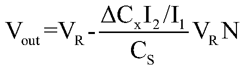 其中,所述V R为所述参考电压,所述ΔC x为所述检测电容器相对于参考电容值的变化量,所述C S为所述积分电容器的电容值,所述I 1为所述第一电流源的电流值,所述I 2为所述第二电流源的电流值,所述N为所述充放电阶段至所述第二缓冲阶段的执行次数。 Wherein, the V R is the reference voltage, the ΔC x is a change amount of the detection capacitor relative to a reference capacitance value, the C S is a capacitance value of the integration capacitor, and the I 1 is the a current value of the first current source, the I 2 is a current value of the second current source, and the N is a number of executions of the charging and discharging phase to the second buffering phase.
 - 根据权利要求2所述的电容检测电路,所述充放电开关组包括第一开关、第二开关、第三开关和第四开关,所述积分开关组包括第五开关,所述清零开关组包括第六开关;The capacitance detecting circuit according to claim 2, wherein the charge and discharge switch group includes a first switch, a second switch, a third switch, and a fourth switch, the integral switch group includes a fifth switch, and the clear switch group Including a sixth switch;所述第一开关的一端连接所述第一电流源的一端,所述第一电流源的另一端接地,所述第一开关的另一端连接所述检测电容器的一端以及所述第三开关的一端,所述检测电容器的另一端接地,所述第三开关的另一端连接电源电压;One end of the first switch is connected to one end of the first current source, the other end of the first current source is grounded, and the other end of the first switch is connected to one end of the detecting capacitor and the third switch One end, the other end of the detecting capacitor is grounded, and the other end of the third switch is connected to a power supply voltage;所述第二开关的一端连接所述第二电流源的一端,所述第二电流源的另一端接地,所述第二开关的另一端连接所述校准电容器的一端以及所述第四开关的一端,所述校准电容器的另一端接地,所述第四开关的另一端连接电源电压;One end of the second switch is connected to one end of the second current source, the other end of the second current source is grounded, and the other end of the second switch is connected to one end of the calibration capacitor and the fourth switch One end, the other end of the calibration capacitor is grounded, and the other end of the fourth switch is connected to a power supply voltage;所述第五开关的一端连接所述校准电容器的一端,所述第五开关的另一端连接所述放大器的第一输入端,所述放大器的第二输入端用于输入所述参考电压;One end of the fifth switch is connected to one end of the calibration capacitor, the other end of the fifth switch is connected to the first input end of the amplifier, and the second input end of the amplifier is used for inputting the reference voltage;所述第六开关与所述积分电容器并联连接,所述积分电容器与所述放大器并联连接。The sixth switch is connected in parallel with the integrating capacitor, and the integrating capacitor is connected in parallel with the amplifier.
- 根据权利要求8所述的电容检测电路,其特征在于,在所述电荷清零阶段,所述第六开关闭合,所述第一开关、所述第二开关、所述第三开关、所述第四开关和所述第五开关都断开,清零所述积分电容器上存储的电荷;The capacitance detecting circuit according to claim 8, wherein in said charge clearing phase, said sixth switch is closed, said first switch, said second switch, said third switch, said The fourth switch and the fifth switch are both turned off, and the charge stored on the integrating capacitor is cleared;所述充放电阶段包括充电阶段和放电阶段,所述充电阶段在所述放电阶段之前,其中:The charge and discharge phase includes a charge phase and a discharge phase, the charge phase being prior to the discharge phase, wherein:在所述充电阶段,所述第三开关和第四开关闭合,所述第一开关、所述 第二开关、所述第五开关和所述第六开关都断开,所述检测电容器和所述校准电容器上的电压都被充电至所述电源电压;In the charging phase, the third switch and the fourth switch are closed, the first switch, the second switch, the fifth switch, and the sixth switch are both turned off, the detecting capacitor and the The voltage on the calibration capacitor is charged to the supply voltage;在所述放电阶段,所述第一开关和所述第二开关闭合,所述第三开关、所述第四开关、所述第五开关和第六开关都断开,所述检测电容器上的电压从所述电源电压被放电至所述参考电压,在所述检测电容器上的电压被放电至所述参考电压之后,所述第一开关和所述第二开关断开;In the discharging phase, the first switch and the second switch are closed, and the third switch, the fourth switch, the fifth switch, and the sixth switch are both turned off, on the detecting capacitor a voltage is discharged from the power supply voltage to the reference voltage, and after the voltage on the detection capacitor is discharged to the reference voltage, the first switch and the second switch are turned off;在所述电荷转移阶段,所述第一开关、所述第二开关、所述第三开关、所述第四开关和所述第六开关都断开,所述第五开关闭合,所述校准电容器上的部分电荷转移到所述积分电容器。In the charge transfer phase, the first switch, the second switch, the third switch, the fourth switch, and the sixth switch are both turned off, the fifth switch is closed, and the calibration A portion of the charge on the capacitor is transferred to the integrating capacitor.
- 根据权利要求9所述的电容检测电路,其特征在于,在所述充放电阶段和所述电荷转移阶段之间还包括第一缓冲阶段,在所述电荷转移阶段之后还包括第二缓冲阶段,所述第一缓冲阶段和所述第二缓冲阶段用于保持所述检测电容器、所述校准电容器和所述积分电容上的电荷不变;The capacitance detecting circuit according to claim 9, further comprising a first buffering phase between said charging and discharging phase and said charge transferring phase, further comprising a second buffering phase after said charge transferring phase The first buffering phase and the second buffering phase are for maintaining a constant charge on the detection capacitor, the calibration capacitor, and the integration capacitor;其中,在所述第一缓冲阶段和所述第二缓冲阶段,所述第一开关、所述第二开关、所述第三开关、所述第四开关、所述第五开关和所述第六开关都断开。Wherein, in the first buffering phase and the second buffering phase, the first switch, the second switch, the third switch, the fourth switch, the fifth switch, and the first The six switches are all disconnected.
- 根据权利要求10所述的电容检测电路,其特征在于,所述控制模块还用于:The capacitance detecting circuit according to claim 10, wherein the control module is further configured to:控制所述充放电开关组、所述积分开关组和所述清零开关组多次重复执行从所述充放电阶段至所述第二缓冲阶段中的操作。Controlling the charge and discharge switch group, the integral switch group, and the clear switch group repeatedly performs operations from the charge and discharge phase to the second buffer phase.
- 根据权利要求11所述的电容检测电路,其特征在于,所述积分器的输出电压V out为: The capacitance detecting circuit according to claim 11, wherein the output voltage V out of the integrator is:
 其中,V R为所述参考电压,所述ΔC x为所述检测电容器相对于参考电容值的变化量,所述C S为所述积分电容器的电容值,所述I 1为所述第一电流源的电流值,所述I 2为所述第二电流源的电流值,所述V DD为所述电源电压,所述N为所述充放电阶段至所述第二缓冲阶段的执行次数。 Wherein, V R is the reference voltage, the ΔC x is a change amount of the detection capacitor relative to a reference capacitance value, the C S is a capacitance value of the integration capacitor, and the I 1 is the first a current value of the current source, the I 2 is a current value of the second current source, the V DD is the power supply voltage, and the N is the number of executions of the charging and discharging phase to the second buffering phase .
 - 根据权利要求1至12中任一项所述的电容检测电路,其特征在于,所述电容检测电路还包括比较器,所述比较器的第一输入端连接所述检测电容器,所述比较器的第二输入端用于输入所述参考电压,所述比较器的输出 端连接所述控制模块;The capacitance detecting circuit according to any one of claims 1 to 12, wherein the capacitance detecting circuit further comprises a comparator, a first input terminal of the comparator is connected to the detecting capacitor, and the comparator The second input terminal is configured to input the reference voltage, and the output end of the comparator is connected to the control module;在所述检测电容器的电压达到所述参考电压时,所述比较器的输出信号发生翻转,所述控制模块控制所述充放电模块停止对所述检测电容器和所述校准电容器进行充电或放电。The output signal of the comparator is inverted when the voltage of the detecting capacitor reaches the reference voltage, and the control module controls the charging and discharging module to stop charging or discharging the detecting capacitor and the calibration capacitor.
- 根据权利要求1至13中任一项所述的电容检测电路,其特征在于,所述电容检测电路还包括处理模块,用于根据所述积分器的输出电压确定所述检测电容器的电容值相对于参考电容值的变化量。The capacitance detecting circuit according to any one of claims 1 to 13, wherein the capacitance detecting circuit further comprises a processing module, configured to determine, according to an output voltage of the integrator, a capacitance value of the detecting capacitor relative to The amount of change in the reference capacitance value.
- 根据权利要求1至14中任一项所述的电容检测电路,其特征在于,所述校准电容器用于在所述检测电容器的电容值为参考电容值时使得所述积分器的输出电压为参考电压,其中,所述参考电容值和所述校准电容器的电容值的比值等于所述第一电流源的电流值和所述第二电流源的电流值的比值。The capacitance detecting circuit according to any one of claims 1 to 14, wherein the calibration capacitor is configured to make an output voltage of the integrator a reference when a capacitance value of the detecting capacitor is a reference capacitance value a voltage, wherein a ratio of the reference capacitance value to a capacitance value of the calibration capacitor is equal to a ratio of a current value of the first current source to a current value of the second current source.
- 根据权利要求1至15中任一项所述的电容检测电路,其特征在于,所述第一电流源的电流值大于所述第二电流源的电流值。The capacitance detecting circuit according to any one of claims 1 to 15, wherein a current value of the first current source is greater than a current value of the second current source.
- 根据权利要求1至16中任一项所述的电容检测电路,其特征在于,所述电容检测电路应用于电容传感器中,所述检测电容器为所述电容传感器的传感器电容,未操作所述电容传感器时所述传感器电容的电容值为参考电容值。The capacitance detecting circuit according to any one of claims 1 to 16, wherein the capacitance detecting circuit is applied to a capacitance sensor, the detecting capacitor is a sensor capacitance of the capacitive sensor, and the capacitor is not operated The capacitance of the sensor capacitor is the reference capacitance value when the sensor is used.
- 一种触控装置,其特征在于,包括:A touch device, comprising:如权利要求1至17中任一项所述的电容检测电路。A capacitance detecting circuit according to any one of claims 1 to 17.
- 一种终端设备,其特征在于,包括:A terminal device, comprising:如权利要求1至17中任一项所述的电容检测电路。A capacitance detecting circuit according to any one of claims 1 to 17.
Priority Applications (5)
| Application Number | Priority Date | Filing Date | Title |
|---|---|---|---|
| CN201880003881.9A CN110300897B (en) | 2018-01-24 | 2018-01-24 | Capacitance detection circuit, touch device and terminal equipment |
| KR1020207021178A KR102337627B1 (en) | 2018-01-24 | 2018-01-24 | Capacitance detection circuit, touch device and terminal device |
| EP18877306.3A EP3543716B1 (en) | 2018-01-24 | 2018-01-24 | Capacitance detection circuit, touch apparatus, and terminal device |
| PCT/CN2018/073907 WO2019144303A1 (en) | 2018-01-24 | 2018-01-24 | Capacitance detection circuit, touch apparatus, and terminal device |
| US16/419,074 US10845926B2 (en) | 2018-01-24 | 2019-05-22 | Capacitance detecting circuit, touch device and terminal device |
Applications Claiming Priority (1)
| Application Number | Priority Date | Filing Date | Title |
|---|---|---|---|
| PCT/CN2018/073907 WO2019144303A1 (en) | 2018-01-24 | 2018-01-24 | Capacitance detection circuit, touch apparatus, and terminal device |
Related Child Applications (1)
| Application Number | Title | Priority Date | Filing Date |
|---|---|---|---|
| US16/419,074 Continuation US10845926B2 (en) | 2018-01-24 | 2019-05-22 | Capacitance detecting circuit, touch device and terminal device |
Publications (1)
| Publication Number | Publication Date |
|---|---|
| WO2019144303A1 true WO2019144303A1 (en) | 2019-08-01 |
Family
ID=67395822
Family Applications (1)
| Application Number | Title | Priority Date | Filing Date |
|---|---|---|---|
| PCT/CN2018/073907 WO2019144303A1 (en) | 2018-01-24 | 2018-01-24 | Capacitance detection circuit, touch apparatus, and terminal device |
Country Status (5)
| Country | Link |
|---|---|
| US (1) | US10845926B2 (en) |
| EP (1) | EP3543716B1 (en) |
| KR (1) | KR102337627B1 (en) |
| CN (1) | CN110300897B (en) |
| WO (1) | WO2019144303A1 (en) |
Cited By (1)
| Publication number | Priority date | Publication date | Assignee | Title |
|---|---|---|---|---|
| EP3786912A1 (en) * | 2019-08-27 | 2021-03-03 | Nxp B.V. | Integrated circuit and measurement method |
Families Citing this family (11)
| Publication number | Priority date | Publication date | Assignee | Title |
|---|---|---|---|---|
| CN111488083B (en) * | 2019-01-25 | 2023-03-31 | 瑞昱半导体股份有限公司 | Capacitive touch detection device with self-calibration function |
| CN111142705B (en) * | 2019-12-18 | 2023-09-08 | 基合半导体(宁波)有限公司 | Self-capacitance detection device and method and mobile terminal |
| KR102623568B1 (en) | 2020-03-03 | 2024-01-11 | 선전 구딕스 테크놀로지 컴퍼니, 리미티드 | Capacitance detection circuits, sensors, chips and electronics |
| CN111638015B (en) * | 2020-06-29 | 2022-05-17 | 歌尔科技有限公司 | Water inflow detection device and method of interface equipment |
| CN112485640B (en) * | 2020-11-18 | 2023-06-27 | 苏州华兴源创科技股份有限公司 | Method, device, equipment and storage medium for detecting built-in capacitor |
| CN113126817A (en) * | 2021-03-12 | 2021-07-16 | 曜芯科技有限公司 | Capacitance sensing circuit, related chip and touch device |
| US11868173B2 (en) * | 2021-08-19 | 2024-01-09 | Marvell Asia Pte Ltd | Wireline transceiver with internal and external clock generation |
| CN114184986A (en) * | 2021-10-29 | 2022-03-15 | 浪潮(北京)电子信息产业有限公司 | Capacitor abnormity detection device and server |
| CN114460360B (en) * | 2022-04-12 | 2022-07-01 | 江西西平计量检测有限公司 | Detection method, system and device based on ammeter measurement current time integral |
| CN116317545B (en) * | 2023-05-11 | 2023-08-08 | 上海泰矽微电子有限公司 | Negative-pressure charge transfer circuit and capacitive touch detection circuit |
| CN117220659A (en) * | 2023-09-06 | 2023-12-12 | 深圳市航顺芯片技术研发有限公司 | Touch key detection method, circuit and electronic equipment |
Citations (4)
| Publication number | Priority date | Publication date | Assignee | Title |
|---|---|---|---|---|
| CN1189719A (en) * | 1996-11-15 | 1998-08-05 | 阿尔卑斯电气株式会社 | Weak current monitoring circuit and coordinate input device of utilizing the same |
| CN101477152A (en) * | 2008-12-24 | 2009-07-08 | 北京希格玛和芯微电子技术有限公司 | Capacitance detection apparatus and method |
| CN101943716A (en) * | 2009-07-09 | 2011-01-12 | 联咏科技股份有限公司 | Capacitance measurement circuit and method |
| CN102314268A (en) * | 2010-06-30 | 2012-01-11 | 盛群半导体股份有限公司 | Capacitance-type touch device |
Family Cites Families (16)
| Publication number | Priority date | Publication date | Assignee | Title |
|---|---|---|---|---|
| JPH0638088B2 (en) * | 1985-08-05 | 1994-05-18 | 新日本製鐵株式会社 | Capacitance measurement circuit |
| JP2002033651A (en) * | 2000-07-17 | 2002-01-31 | Mitsubishi Electric Corp | Load capacitance measurement circuit and output buffer |
| EP1677084A1 (en) * | 2004-12-22 | 2006-07-05 | Roxer Industries S.A. | LIquid level sensor and method of estimation |
| WO2006133594A1 (en) * | 2005-04-30 | 2006-12-21 | Apexone Microelectronics Inc. | Circuit and process for power management |
| DE102005061090B3 (en) * | 2005-12-21 | 2007-08-30 | Atmel Germany Gmbh | Measuring device for capacitive pressure measurement |
| GB2436389A (en) * | 2006-03-23 | 2007-09-26 | Sharp Kk | Active matrix liquid crystal device with temperature measuring capacitor |
| TWI380203B (en) * | 2008-09-19 | 2012-12-21 | Chimei Innolux Corp | Sensing circuit discharge control method and device for touch panel |
| CN102253289B (en) * | 2010-05-18 | 2013-12-25 | 联咏科技股份有限公司 | Electric capacity measuring device for touch control device |
| JP2013088382A (en) | 2011-10-21 | 2013-05-13 | Asahi Kasei Electronics Co Ltd | Electrostatic capacitance detection circuit and signal processing circuit for touch sensor |
| CN103324366B (en) | 2012-03-20 | 2016-09-28 | 晨星软件研发(深圳)有限公司 | Capacitance detecting device and apply the capacitance touch control system of this capacitance detecting device |
| US8896327B2 (en) | 2012-04-12 | 2014-11-25 | Atmel Corporation | Current mirror self-capacitance measurement |
| US9372582B2 (en) | 2012-04-19 | 2016-06-21 | Atmel Corporation | Self-capacitance measurement |
| US9310924B2 (en) | 2012-09-26 | 2016-04-12 | Atmel Corporation | Increasing the dynamic range of an integrator based mutual-capacitance measurement circuit |
| JP2015141556A (en) * | 2014-01-29 | 2015-08-03 | シナプティクス・ディスプレイ・デバイス合同会社 | Touch detection circuit and semiconductor integrated circuit having the same |
| TWI574193B (en) * | 2016-05-13 | 2017-03-11 | 九齊科技股份有限公司 | Touch sensing device |
| CN206440771U (en) * | 2017-01-18 | 2017-08-25 | 深圳市汇顶科技股份有限公司 | Detect the device, electronic equipment and the device for detecting pressure of electric capacity |
-
2018
- 2018-01-24 CN CN201880003881.9A patent/CN110300897B/en active Active
- 2018-01-24 EP EP18877306.3A patent/EP3543716B1/en active Active
- 2018-01-24 WO PCT/CN2018/073907 patent/WO2019144303A1/en unknown
- 2018-01-24 KR KR1020207021178A patent/KR102337627B1/en active IP Right Grant
-
2019
- 2019-05-22 US US16/419,074 patent/US10845926B2/en active Active
Patent Citations (4)
| Publication number | Priority date | Publication date | Assignee | Title |
|---|---|---|---|---|
| CN1189719A (en) * | 1996-11-15 | 1998-08-05 | 阿尔卑斯电气株式会社 | Weak current monitoring circuit and coordinate input device of utilizing the same |
| CN101477152A (en) * | 2008-12-24 | 2009-07-08 | 北京希格玛和芯微电子技术有限公司 | Capacitance detection apparatus and method |
| CN101943716A (en) * | 2009-07-09 | 2011-01-12 | 联咏科技股份有限公司 | Capacitance measurement circuit and method |
| CN102314268A (en) * | 2010-06-30 | 2012-01-11 | 盛群半导体股份有限公司 | Capacitance-type touch device |
Cited By (2)
| Publication number | Priority date | Publication date | Assignee | Title |
|---|---|---|---|---|
| EP3786912A1 (en) * | 2019-08-27 | 2021-03-03 | Nxp B.V. | Integrated circuit and measurement method |
| US11500003B2 (en) | 2019-08-27 | 2022-11-15 | Nxp B.V. | Integrated circuit and measurement method |
Also Published As
| Publication number | Publication date |
|---|---|
| CN110300897A (en) | 2019-10-01 |
| KR20200101435A (en) | 2020-08-27 |
| US20190272056A1 (en) | 2019-09-05 |
| EP3543716A4 (en) | 2020-01-29 |
| US10845926B2 (en) | 2020-11-24 |
| EP3543716A1 (en) | 2019-09-25 |
| EP3543716B1 (en) | 2021-03-03 |
| CN110300897B (en) | 2020-11-03 |
| KR102337627B1 (en) | 2021-12-09 |
Similar Documents
| Publication | Publication Date | Title |
|---|---|---|
| WO2019144303A1 (en) | Capacitance detection circuit, touch apparatus, and terminal device | |
| US9652104B2 (en) | Capacitance voltage conversion circuit, input apparatus using the same, electronic instrument, and capacitance voltage conversion method | |
| EP3502855B1 (en) | Capacitance detection device, touch device and terminal device | |
| CN111801584B (en) | Capacitance detection circuit, touch device and terminal equipment | |
| CN208013309U (en) | Capacitive detection circuit, touch device and terminal device | |
| US10949032B2 (en) | Circuit, touch chip, and electronic device for capacitance detection | |
| CN107449810B (en) | Capacitance measuring circuit, input device using the same, and electronic apparatus | |
| US10641805B2 (en) | Capacitance detection method and capacitance detection apparatus using the same | |
| CN104965627B (en) | Touch detection circuit and semiconductor integrated circuit provided with same | |
| US10921938B2 (en) | Capacitance detecting circuit, touch detecting device and terminal device | |
| KR20140030170A (en) | Active integrator for a capacitive sense array | |
| JP2011170617A (en) | Electrostatic capacity type touch sensor | |
| CN110596465B (en) | Capacitance detection circuit, touch device and terminal equipment | |
| JP2020086743A (en) | Touch detection circuit, input device, and electronic device | |
| TW201519054A (en) | Capacitive touch sensor and switching method between self capacitance and mutual capacitance therefor | |
| CN214473623U (en) | Capacitance detection circuit | |
| JP6510343B2 (en) | Capacitance measurement circuit, input device using it, electronic device | |
| WO2019169555A1 (en) | Circuit for capacitance detection, touch detection device, and terminal apparatus | |
| TWI381300B (en) | Touch panel, touch display panel, and conpacitive touch sensor | |
| US9329736B2 (en) | Capacitive touch panel input device that measures internal resistances for compensation | |
| WO2020001283A1 (en) | Active pen, touch input system, and driving method | |
| JP2002108553A (en) | Circuit for generating touch detection signal and method for the same and coordinate inputting device |
Legal Events
| Date | Code | Title | Description |
|---|---|---|---|
| ENP | Entry into the national phase |
Ref document number: 2018877306 Country of ref document: EP Effective date: 20190522 |
|
| ENP | Entry into the national phase |
Ref document number: 20207021178 Country of ref document: KR Kind code of ref document: A |
|
| NENP | Non-entry into the national phase |
Ref country code: DE |